1
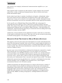
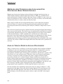
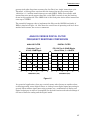
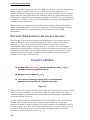
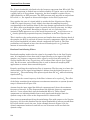
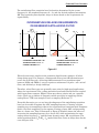
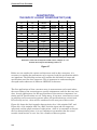
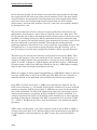
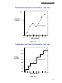
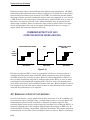
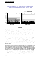
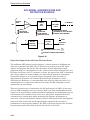
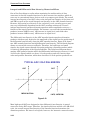
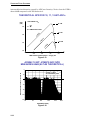
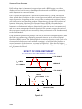
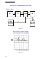
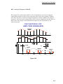
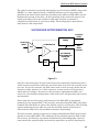
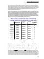
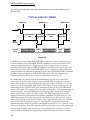
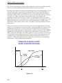
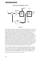
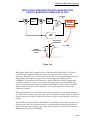
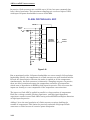
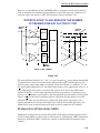
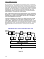
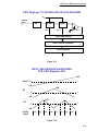
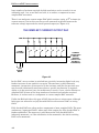
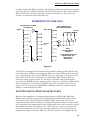
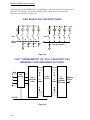
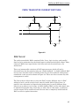
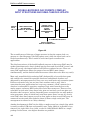
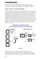
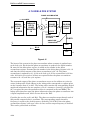
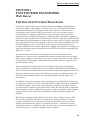
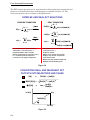
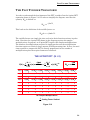
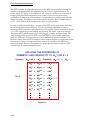
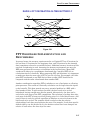
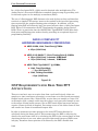
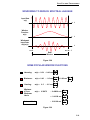
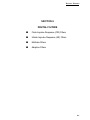
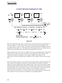
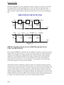
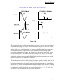
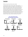
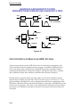
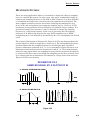
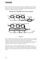
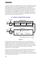
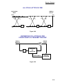
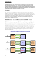
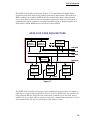
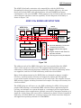
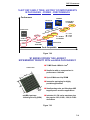
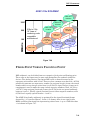
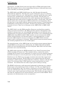
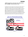
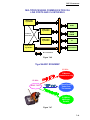
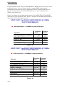
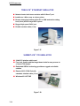
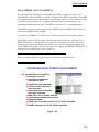
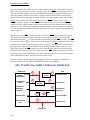
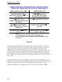
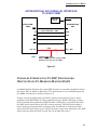
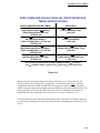
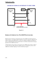
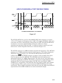
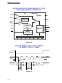
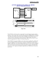
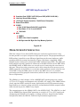
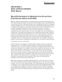
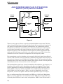
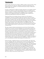
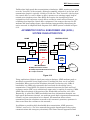
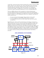
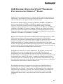
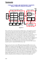
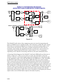
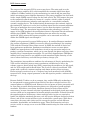
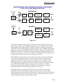
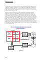
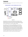
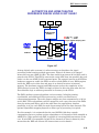
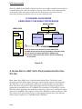
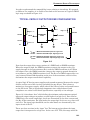
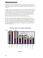
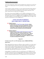
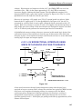
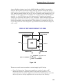
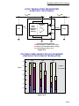
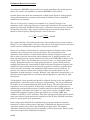
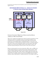
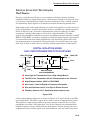
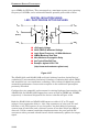
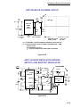
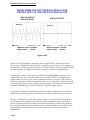
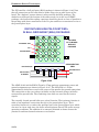
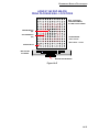
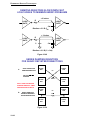
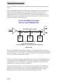
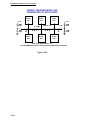
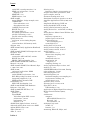
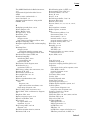
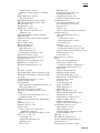
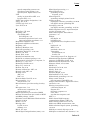
INTERFACING TO DSPS
ADSP-2189M PARALLEL WRITE TIMING
■ tCK = Processor Clock Period (13.3ns)
■ tASW = Address and Memory Select Before WR Low
= 0.25tCK – 3ns Minimum
■ tDW = Data Setup Before WR High = 0.5tCK – 4ns + # Wait States × tCK
■ tDH = Data Hold After WR High = 0.25tCK – 1ns
■ tWP = WR Pulse Width = 0.5tCK – 3ns + # Wait States × tCK Minimum
Figure 8.11
The AD5340 is a 12 bit 100kSPS DAC which has a parallel data interface. It
operates on a single +2.5V to +5.5V supply and dissipates only 345µW (+3V supply).
A power-down mode further reduces the power to 0.24µW. The part incorporates an
on-chip output buffer which can drive the output to both supply rails. The AD5340
allows the choice of a buffered or unbuffered reference input. The device has a
power-on reset circuit that ensures that the DAC output powers on at 0V and
remains there until valid data is written to the part. A block diagram is shown in
Figure 8.12. The input is double buffered. The key interface timing specifications for
the two devices are compared in Figure 8.13. Specifications for the ADSP-2189M are
given for a clock frequency of 75MHz.
AD5340 12-BIT, 100kSPS PARALLEL INPUT DAC
VREF
POWER-ON
RESET
DB0
BUF
GAIN
CS
WR
INTERFACE LOGIC
DB11
INPUT
REGISTER
DAC
REGISTER
12-BIT
DAC
RESET
CLR
POWER-DOWN
LOGIC
LDAC
PD
Figure 8.12
8.10
VOUT
BUF
GND