1
FILE MANAGEMENT OF A USB FLASH DRIVE
AND MEMORY CARD VIA MICRO SD
CARD SLOT OF A MOBILE PHONE
By
Meryl Filomena B. Coching
Kristine Doctor
Francis Mark V. Evangelista
Lynda Clarissa C. Santos
A Design Report Submitted to the School of Electrical Engineering,
Electronics Engineering, and Computer Engineering in Partial
Fulfilment of the Requirements for the Degree
Bachelor of Science in Computer Engineering
Mapua Institute of Technology
October 2011
i
ii
TABLE OF CONTENTS
TITLE PAGE
i
APPROVAL SHEET
ii
TABLE OF CONTENTS
iii
LIST OF TABLES
v
LIST OF FIGURES
vi
ABSTRACT
vii
Chapter 1: DESIGN BACKGROUND AND INTRODUCTION
1
Background
Statement of the Problem
Objectives of the Design
Impact of the Design
Design Constraints
Definition of terms
1
2
3
4
5
6
Chapter 2: REVIEW OF RELATED LITERATURE AND RELATED STUDIES
8
Chapter 3: DESIGN PROCEDURES
21
Conceptual Diagram
Block Diagram
Schematic Diagram
Program Flowchart
Prototype Development
21
23
25
28
30
Chapter 4: TESTING, PRESENTATION, AND INTERPRETATION OF DATA
36
Chapter 5: CONCLUSION AND RECOMMENDATION
45
Conclusion
Recommendation
45
46
BIBLIOGRAPHY
47
APPENDIX
49
iii
A. Operation’s Manual
1. System Requirement
2. Installation Procedure
3. User’s Manual
4. Troubleshooting Guides and Procedures
5. Error Definitions
B. Complete Set of Data Sheets
C. Program Listing
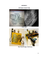
D. Pictures of Prototype
E. IEEE Format Article of the Design
49
49
49
50
51
52
53
100
102
104
iv
List of Tables
Table 4.1: File Copy Speed Test Results using Phone Model
Nokia C3 at file size of 1 MB
38
Table 4.2: File Copy Speed Test Results using Phone Model
Nokia C3 at file size of 10 MB
40
Table 4.3: Average Transfer Speed at 1 MB and 10 MB
41
Table 4.4: Variance and Standard Deviation at 1 MB and 10 MB
42
v
List of Figures
Figure 3.1: Conceptual Diagram of the Design
21
Figure 3.2: Block Diagram of the Design
23
Figure 3.3: Schematic Diagram of the Design
25
Figure 3.4: Program Flowchart
28
Figure 3.5: SD Memory Card Slot & Pin-out
32
Figure 3.6: micro SD Sniffer
34
vi
ABSTRACT
Most of modern mobile phones have a micro SD slot that is used for expanded
storage. Inspired by the recently released Nokia N8 which has a USB On-the-Go
feature that allows a flash drive to be connected via a cable used, the
researchers constructed a design wherein the micro SD slot is used as a pathway
to incorporate the USB port and the memory card port/s. The purpose of the
design is to give the mobile phone additional storage and to access/transfer data
using another media, in substitute for desktop PCs particularly. The flash drive to
be used should comply with USB 2.0 and the memory card is limited to SD/mini
SD with maximums of 2GB and 4GB total space limit respectively. The device is
intended for mobile phones with a micro SD slot. The major hardware
components of the design consist of SD memory slots, USB to SDIO Bridge Chip
Host interface Transfer for the USB flash drive, relay circuits and a
microcontroller which is programmed for port switching and a micro SD sniffer
for the main output device. The single file copy speed test is conducted to test
the functionality of the device. The transfer speeds for each flash memory are
also looked upon and was observed that compared to the theoretical data
transfer rates for the USB flash drive and SD memory card to the computer, the
data transfer rates from the said flash memories with respect to the researchers
device are acceptable. After testing the prototype, the researchers satisfied the
assumptions that the file management is successful and the file integrity is
preserved.
Keywords: micro SD, USB 2.0, USB On-the-Go, SD memory card, File Transfer
vii
Chapter 1
DESIGN BACKGROUND AND INTRODUCTION
Background
Mobile phones have limited capabilities to access storage devices such as thumb
drives and other memory cards that do not fit into the phone except card slots
installed on the phone. Most of phones today have micro SD memory card slots
installed. Almost all people nowadays have mobile phones, and almost all people
have the need to transfer files quickly and want to ensure that data are
successfully sent. As of now, the available media to send files are via infrared,
Bluetooth, and one card slot that depends on what is installed on the phone. But
what if the files needed are saved on a USB flash drive, SD memory card or mini
SD memory card? Let’s say one’s phone only accepts a micro SD memory card.
One solution is to have a computer to access files to transfer to one’s phone. Not
all people carry their laptops all the time; or to have access to a PC.
A memory card (sometimes called a flash memory card or a storage card) is a
small storage medium used to store data such as text, pictures, audio, and
video, for use on small, portable or remote computing devices. Most of the
current products use flash memory, although other technologies are being
developed. Memory cards offer a number of advantages over the hard disk drive:
they're much smaller and lighter, extremely portable, completely silent, allow
more immediate access, and are less prone to mechanical damage. A USB flash
drive is portable memory storage. It is re-writeable and holds its memory without
1
a power supply, unlike RAM. USB flash drives will fit into any USB port on a
computer. For a USB flash drive to function, it needs a host controller. Just like a
PC, all flash drives have a storage device controller for it to read the device. This
functionality is lacking in mobile phones since phones do not have a USB host
controller.
This design is intended for on the go use. The user can simply insert the storage
device and can easily manage files on their phones and the storage device. The
phone will read the storage device as a memory card that is inserted in its
memory card slot. Only one storage device can be read at a given time. To do
this, there is a switch for every device wherein the users can mount the storage
device they want to use. The design has a switching capability to choose what
device is mounted.
The major components of this design are the SD card slots and USB flash drive
slot wherein the user can insert a storage device. The design has a micro SD
card sniffer so that the phone can access the storage inserted through this micro
SD card sniffer. Switching components are used to access just one USB flash
drive or either one of the memory cards at a time, because phones have a
limited capability to read simultaneously storage devices.
Statement of the Problem
Being students of Mapua Institute of Technology, the researchers continue to
find ways to make life easy by innovating current technology advancements. This
study’s topic is mainly concerned with portable storage devices and mobile
2
phones. There is a need for a multi-purpose USB plus memory card reader/writer
to host demanding storage applications and on-the-go access of the data.
The design is inspired by the fact that modern mobile phones like smart phones
use the general purpose micro SD slot for data storage which limits the capability
of the mobile phone to store data on other portable storage media like flash
drives or other memory cards. Additionally, USB OTG (on-the-go) which is used
by Nokia N8 to access/transfer data using a flash drive is limited only in their
platform while other manufacturers of mobile phones do not incorporate such
technology in their devices.
Objectives of the Design
The main objective of this study is to design and construct a device that can
manage files in a USB flash drive and memory card in a mobile phone via its
micro SD card slot”. Its specific objectives are as follows:
To construct the main circuitry of the device which will consist of the design’s
input, process, and output.
To create the prototype that will be able to route the data inside the flash
memory for a specific destination.
To create a program that will make the device capable of responding to the
user’s selection of which flash memory device is to be activated in the mobile
phone.
To test if the device is capable of managing files between the mobile phone and
the activated flash memory device.
3
To verify that the data transferred to and from the device is intact with no
corruption.
Impact of the design
The significance of this design is to provide people a flexible way of transferring
data. Mobile phones are limited to the use of memory cards, although nowadays
some mobile phones have a micro USB port that supports USB OTG (on-the-go)
that allows USB flash drives including external hard drives to be connected.
However, only a few models have this feature and people are forced or enticed
to buy them, which are quite expensive. More widespread are mobile phones
that have a memory card; however these are restricted to the space they
provide and users of these phones need to buy another memory card or delete
some files if they need more space. People who need additional storage in
different kinds of media will benefit from the proposed device because they will
not be limited to the space that their memory card provides; they do not need to
buy a new mobile phone and they do not need to worry if they need to access a
file.
The design will not be costly to implement. The embedded system only uses a
small of amount of power to operate, the carbon footprint is minimal and
resource utilization is low so no significant harmful effects contribute to the
environment. Ethically, people will refrain from using and bringing their PCs just
to transfer data because mobile phones are much more portable than PCs.
Health and safety concerns will not be likely a problem because the design does
4
not emit harmful radiation. The design manufacturability is high especially when
developed with surface mount technology and finally sustainability will be longterm due to modern mobile phones’ heavy reliance on micro SD technology.
Design Constraints
The design covers the USB and memory card slot/s that can be accessed using
mobile phones with a micro SD slot.
The design utilizes the PIC microcontroller to manage the selection of which will
route the data that will go through.
It is powered by a DC battery or adaptor due to the power requirements of the
PIC microcontroller.
There are one USB port and two SD/MMC memory card ports.
The mobile phone can read all files of different types inside the activated flash
memory to perform different file management features.
The design will utilize the Nokia C3 as the mobile phone model in the testing part
of this study.
The following are the design constraints:
The USB flash drive to be used should be compliant with USB 2.0 standard or
lower.
The USB flash drive to be used is limited to 4 GB of total memory space.
Mobile phones with micro SD slots are supported unless the memory card slot is
located at the back of the device.
5
The memory card slot supports a mini SD with an adapter attached and SDs of
up to 8GB total memory space.
All files inside the USB flash drive or memory card can be read but cannot be
opened or executed unless they are supported by the mobile phone (e.g. mp3 or
jpg files )
The size of the files to be transferred from the activated flash memory depends
on the internal memory capacity of the mobile phone. Nowadays, mobile phones
with micro SD slots have up to 8 GB internal mass memory.
Definition of terms
Microcontrollers - are dedicated to one task and run one specific program. The
program is stored in ROM (read-only memory) and generally does not change.
Memory card - sometimes called a flash memory card or a storage card, is a
small storage medium used to store data for use on small, portable or remote
computing devices.
USB Host - is where the USB host controller is installed and where the client
software/device driver runs.
The USB Host Controller - is the interface between the host and the USB
peripherals. The host is responsible for detecting the insertion and removal of
USB devices, managing the control and data flow between the host and the
devices, providing power to attached devices, and more.
PDAs– acronym for Personal Digital Assistants. It is a mobile device that
functions as a personal information manager.
6
Flash Memory - is a non-volatile computer storage chip that can be electrically
erased and reprogrammed. Types of flash memory are USB flash drives and SD
memory cards.
EEPROM - stands for Electrically Erasable Programmable Read-Only Memory
and is a type of non-volatile memory used in computers and other electronic
devices to store small amounts of data that must be saved when power is
removed.
Voltage Amplifier - An amplifier designed primarily to build up the voltage of a
signal, without supplying it.
Serial Port - a serial communication physical interface through which
information transfers in or out one bit at a time.
Biasing - is the method of establishing predetermined voltages and/or currents
at various points of an electronic circuit to set an appropriate operating point.
Voltage drop - is the reduction in voltage in the passive elements (not
containing sources) of an electrical circuit.
Saturation - is the fully conducting state in a semiconductor junction. The term
is used especially in applications involving diodes and bipolar transistors
7
Chapter 2
REVIEW OF RELATED DESIGN LITERATURES AND STUDIES
Digital Memory Card Market and Technology
In recent years, the proliferation of portable consumer electronics such as MP3s,
digital cameras, and3G mobile phones has created a tremendous appetite for
digital memory cards that use non-volatile flash memory for information and data
storage. There are different card formats and designs such as Secure Digital
(SD), mini-SD, MultimediaCards (MMC) and MMCmobile. These cards are
assembled by either a chip-on-board (COB) process using bare dice, or surface
mount technology (SMT) using packaged flash and controller components. The
last step in card assembly is accomplished by using either a pre-mold cover or an
injection mold process over a PCA (Printed Circuit board Assembly. (Wei Koh,
2005
Flash Memory Types
The NOR (Not OR) type flash memory was invented by Fujio Masuoka of Toshiba
in 1984 and Intel developed it further for initial mass production. In 1987
Masuoka also invented the NAND (Not AND) type flash. Because these two kinds
of flash function differently, their applications are suitable for different purposes.
The fundamental reason is due to the cell design of the memory—a NAND cell
size is smaller hence more density can be packed in an IC chip, where as the
NOR flash requires a larger transistor cell, hence lower density on the same sized
8
IC. Due to its faster speed and accuracy, NOR is typically used for code
execution and NAND, being higher capacity but a little lower, is used more for
data storage. The differences between the two types in functionality, however,
are becoming smaller as their design and technology are merging together more
closely in recent years.(Wei Koh, 2005)
Flash Markets
In recent years, the growth of NAND is expanding much faster than NOR. The
applications in portable data storage, the wide popularity and growth in USB
drives and digital still cameras all contribute to the need for more NAND
memory. Whereas for NOR, its use in cell phones is now more limited to low-end
and mid-range phones. For 3G and higher performance multimedia phones, or
so-called smart phones, the trend is now using NAND and DRAM. For low and
mid-range phones, the NOR and PSRAM (pseudo static random access memory)
combination is used for initial phone registration with the base station and for
code executions. For multimedia phones and smart phones, the trend is
switching to the use of the SDRAM/NAND combination to increase memory
storage capability.(Wei Koh, 2005)
Digital Card Formats
The following are the card formats using NAND flash memory for data storage:
Compact Flash (CF), Multimedia Card (MMC), and Secure Digital (SD). Currently,
9
CF card market shares are gradually being taken over by thinner and smaller
cards such as MMC and SD, as the memory density in these cards go up and
increase their storage capacity. In coming years, each card format may come to
be specialized in certain applications. For example, CF cards may concentrate on
very high capacity (4 GB or higher) for use in high resolution (>6 million pixel)
professional, high-end digital still cameras or even camcorders for high volume
recording and storage. On the other end of the spectrum, the thin form factor
cards are becoming even thinner and smaller for portable devices such as
cellphones and multimedia phones or PDAs. The reduction in sizes in MMC—
called MMC-mobile and the miniSD that is about half the size of a regular SD
card--are obviously intended for mobile applications. Most recently, there are
microSDs and MMCmicro. The microSD card is based on SanDisk Transflash
cards. Due to their minuscule sizes, initially, their memory densities are typically
no more than 50% of their respective “mother” cards, or in the range of128/256
MB. With use of MCP (multichip package), however, stacked flash die inside the
card will enable even the smallest cards to have memory densities in the512MB
and even 1GB range.(Wei Koh, 2005)
MMC versus SD
When selecting the types of flash cards for application and devices, performance
and other factors such as license, royalty, security, and standards are all part of
design considerations. Currently MMC and SD cards are the two more dominant
10
formats of choice. The design and performance difference between the two
cards are now nearly equal. One useful factor to note is that, because both MMC
and SD cards have the same outer envelope, the MMC cards can be used in the
same slot for SD cards and most readers are designed to accept both MMC and
SD cards.(Wei Koh, 2005)
Summary
The growth of NAND and NOR-type flash memory cards has been phenomenal in
the past few years with the proliferation of consumer use of portable devices and
digital storage. The flash market in 2005 is $17 billion for both NAND and NOR;
however, NAND growth is expected to outpace NOR and will have higher
revenue in the years to come. Currently, many different card formats are all
growing in popularity, but SD and MMC cards are the leading formats as their
memory density increases while CF cards are becoming more specialized in highend professional digital photography. The fabrication process of MMC and SD
cards is moving toward SIP and MCP, due to continued reduction in card size and
thickness. Of 1.0mm and lower, the main manufacturing challenges include using
a thin die stack, thin substrates and method of forming the final card dimensions
by either applying a thin cover or directly over the mold.
11
USB on-the-go interface for portable devices
Until recently, most portable electronic devices used proprietary wired interfaces
for connecting to a PC, accessories or chargers. Such portable electronic devices
include cell phones, digital cameras, personal digital assistants and mini-USB
plugs. Not only was the mechanical interface different for different models from
different vendors, but so also were the electrical and protocol interfaces.
Proprietary cables and software packages were often required to connect these
devices to PCs and connecting one portable device to another portable device
was generally not possible. In recent years, the processing power and data
storage capacity
of
portable devices has increased
dramatically.
Both
manufacturers and consumers desire a standard data interface on portable
devices in order to allow data sharing between portable devices, and allow the
use of standard cables and accessories. Many of today's portable devices are
moving towards the Universal Serial Bus (USB) electrical interface as a way of
connecting to a PC, although as desktop interface, it is not well suited for
portable devices. The PC acts as host (or master), and all other devices are
peripherals (or slaves). Hosts cannot connect to hosts, and to peripherals.
(Remple, T.B., 2003)
The mini USB plugs are smaller than the standard USB plugs, and are better
suited for portable devices. In standard USB, each cable has a +plug on one
end, and a B-plug on the other end. The A-plug goes to the PC, which acts as
the host or master, and the B-plug goes to the peripheral. This cabling
12
arrangement prevents pc3s (hosts) from being plugged into each other; and also
prevents peripherals from being plugged into each other, works cannot connect
to peripherals. However, when connecting portable devices together, one of the
devices needs to accept a mini.i plug and act as the host, while the other needs
to accept a mini-B plug and act as the peripheral. To avoid requiring portable
devices to have both connectors are too large for portable devices. The mini AB
receptacle accepts either a mini-A plug, or a mini-B plug. A device with a mini-AB
receptacle is referred to as an OTG device. When a mini-A plug is inserted into
an OTG device, it is referred to as an A-device. When a mini-B plug is inserted
into a device, it is referred to as a B-device. The A-device defaults to being the
host when the two devices are first connected. The A-device is always
responsible for outputting power to the B-device. The following are the features
that are required by portable devices, host capability for portable devices smaller
connectors low power features in order for cell phones to use the mini-USB
connectors instead of existing proprietary connectors, and the OTG interface also
has to allow cell phones to connect to analog circuits. (Remple, T.B., 2003)
Host Negotiation Protocol
In order for an OTG device to act as host, it needs to have a software driver that
can recognize and control the peripheral that is connected to it. When two OTG
devices are connected, it is possible that the A-device does not have a software
driver for the B-device, while the B-device does have a driver for the A-device. If
13
the A-device continues to act as host, then the two devices would not be able to
communicate. To address this issue, the OTG Supplement defines a Host
Negotiation Protocol (HNP). HNP allows an A-device and a B-device to swap the
role of host automatically, in a way that is transparent to the user.
Low Power Features
The USB Specification requires that a PC (or A-device) is able to output 500mA.
Moreover, the PC must always provide power to the bus, even when a remote
device is not connected. These requirements are not practical for portable
devices such as cell phones and PDAs. To accommodate portable devices, the
OTG supplement requires an OTG device to output 8mA instead of 500 mA.
Moreover, the A-device is only required to power the bus when the A-device and
B-device are communicating. When the bus is powered down, the B-device
requires a way of notifying the A-device that it wants to communicate. For this
reason, the OTG Supplement defines a Session Request Protocol (SRP). SRP
allows a B-device to request service from the A-device when the bus is powered
down. (Remple, T.B., 2003)
Mini-USB AnalogCarkit Interface
In order for a cell phone to use the mini-USB connector as its primary data
connector, the mini-USB connector must provide an interface to an analogcarkit.
The interface allows several different signaling modes. In all modes, the VBUS
14
and GND pins are used for power. The remaining three pins can be used for
either USB signaling, UART signaling, or analog signaling. The phone determines
which signaling mode it should use by first detecting the state of the ID pin. If
the ID pin is floating or grounded, then the phone uses USB signaling. If the ID
pin is resistively coupled to ground, then the phone knows it is connected to a
carkit. (Remple, T.B., 2003)
Dominant design or multiple designs: The Flash Memory Card case
Any technology currently in use struggled with similar competing products before
gaining the dominant design. The famous case of the VHS videotape is the best
known example of such a battle. The emergence of a dominant design is very
hard to predict and cannot be entirely explained by the economic literature. ‘The
dominant design is not automatically the technologically superior one, nor will it
meet the needs of a particular class to the same extent as a customized design
would’ (Anderson & Tushman, 1990 and Suárez & Utterback, 1995). The
emergence process for dominant designs has typically been viewed as a black
box process involving a sophisticated interaction of technological and nontechnological factors (Lee et al., 1995). There is even a possibility that no
dominant design will emerge, even many years after product introduction.
Examples of cases with no dominant design include: Smartphones, PDA phones,
Blackberry, regular and advanced cell phones (including clock, photo camera,
agenda); HDTV, regular LCD and the plasma screens; Microsoft Xbox, Nintendo
15
Wii, Playstation 3;DVD-R, DVD-RW, DVD-RAM, DVD-D, DVD+R, DVD+RW,
DVD+R DL, HD-DVD and Blu-ray. (deVries, H.J., de Ruijter, J.P.M., & Argam, N.,
2007)
Available flash memory cards
The most common data storage technology is the magnetic disk or hard disk.
Beyond these systems, optical systems are recognized as dominant in archival
digital data storage. Despite their numerous virtues, these systems also come
with several disadvantages. For example, the magnetic and optical data storage
systems are not always perfect, especially in small devices with limited power
supply. To avoid these disadvantages, flash memory is a good alternative. A
flash memory card differs from existing memory storage in that it needs no
power supply (nonvolatile) and can be found in a wide range of portable
electronic devices. There are a number of industrial standards for memory cards.
Different companies produce different types of memory cards, all with different
dimensions. In general, these different types are not interchangeable. Currently,
roughly six types of flash memory cards exist.
1. CompactFlash (CF). CF was introduced by Sandisk Corporation in 1994.
Currently, CF is offered by multiple manufacturers. CF is superior in data transfer
rates and capacity, but the large size and (relatively) high power consumption
make it less suitable for small electronic devices, such as mobile phones.
16
2. SmartMedia (SM). SM, owned by Toshiba, was launched in 1996. It was one
of the smallest and the thinnest early memory cards, and maintained the most
favorable cost ratio. It used to be the favourite card for digital cameras.
3. Multi-MediaCard (MMC). MMC was developed by Siemens (Sandisk as well
later on) in 1997. Nowadays, it is offered by multiple manufacturers. MMC micro
is the smallest card in the world, (backwards) compatible with other cards,
without a write or copyright protection (thinner profiled) and it is available to all
developers.
4. Memory Stick (MS). MS was developed and introduced by Sony in 1998. Sony
uses this card for a range of different products and licenses it to other
companies. MS Duo is the small version for pocket devices.
5. Secure Digital Card (SD). SD was introduced by multiple manufacturers in
2001. The SD card is based on the MMC card but includes a built-in security
function and a write protection switch. It is the most common used memory card
because of its small size and low power consumption.
6. Extreme Digital-Picture Card (xD). Olympus and Fujifilm introduced xD in 2002
for use in their cameras.
Compact Flash typically uses flash memory in a standardized enclosure. This
form was first specified and produced by Sandisk in 1994. Compact Flash lacks
the mechanical write protection switch that some other devices have, as seen in
a comparison of memory cards. Compact Flash does not have any built in DRM
or cryptographic features like on some USB flash drives and other formats such
17
as Secure Digital. Such features are rarely used on other cards, however, and are
therefore mostly superfluous. Toshiba launched Smart Media to compete with
MiniCard, CompactFlash, and PC card formats. A Smart Media card consists of a
single NAND flash chip embedded in a thin plastic card (though some higher
capacity cards contain multiple, linked chips).It was one of the smallest and the
thinnest of the early memory cards, and managed to maintain a favorable cost
ratio as compared to the others. It lacks a built-in controller, which keeps the
cost down. This feature later caused problems, since some older devices would
require firmware updates to handle larger capacity cards. The Multi Media Card is
based on Toshiba's NAND-based flash memory, and is therefore much smaller
than earlier systems based on Intel NOR-based memory such as Compact Flash.
MMC originally used a 1-bit serial interface, but newer versions of the
specification allow transfers of 4 or sometimes even 8 bits at a time. (deVries,
H.J., de Ruijter, J.P.M., & Argam, N., 2007)
Digital cards (SD card) still see significant use because MMC cards can be used in
most devices which support SD cards and they are cheaper than SD cards. RSMMC cards (Reduced-Size Multi Media Cards) are smaller MMC cards; by using a
simple mechanical adapter to elongate the card, an RS-MMC card can be used in
any MMC slot. The only significant hardware licensors of RS-MMC cards are Nokia
and Siemens. Sometimes a memory USB-stick is called a memory stick, but in
this study it refers to the brand name of Sony’s flash memory card Memory
Stick™. Memory Stick is a removable flash memory card format. The Memory
18
Stick family includes the Memory Stick PRO, a revision that allows greater
maximum storage capacity and faster file transfer speeds; Memory Stick Duo, a
small-form-factor version of the Memory Stick (including the PRO Duo); and the
even smaller Memory Stick Micro (M2). (deVries, H.J., de Ruijter, J.P.M., &
Argam, N., 2007)
In summary, there are a host of factors indicating one dominant design to
emerge, in particular the network externalities characterizing the market and the
need to exchange cards between different products. However, a combination of
factors at both the supplier and the consumer side outweigh these factors,
instead favoring multiple cards. Some factors at the supplier side make it
attractive for companies to introduce or maintain their own cards, to be used in
own products or for other products as well. Moreover, the speed of technological
development has prompted companies to introduce new cards before a battle
could turn into a victory for one of the designs. At the consumer side, a
combination of two factors make it easy to live with different cards: consumers
buy the host devices and take the related card format for granted rather than
consciously choose a certain card format. Furthermore, gateway technologies
allow them to do this: the compatibility issues can be solved in a relatively easy
way resulting in the advantages related to network externalities to remain.
(deVries, H.J., de Ruijter, J.P.M., & Argam, N., 2007)
19
Memory card address bus design
The need to store large quantities of data and information for a certain period of
time determines the memory capability of a system. In a typical computer
system, the central processing unit (CPU) generates the address of the particular
memory location and places it on the address lines that makeup an address bus.
A memory card has many parallel address lines connected to a number of
memory chips. These memory chips may supply program and data to the CPU or
hold output data from arithmetic calculations or for printed output or displays.
The address bit combination on the address lines determines which word line will
be addressed for a particular operation. The designer must fully understand the
requirements of the memory operation so the necessary address bit combination
occurs at the proper time during the memory cycle.(deVries, H.J., de Ruijter,
J.P.M., & Argam, N., 2007)
20
Chapter 3
DESIGN PROCEDURES
HARDWARE DEVELOPMENT
Conceptual Diagram
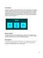
Figure 3.1 – Conceptual Diagram of the Design
The design paradigm shows the relationship between the components involved
in the conceptualization of the file management of a USB flash drive and memory
card via the micro SD card slot of a mobile phone. There are three major parts of
the conceptualized design: the input, which comprises the memory cards and
USB flash drive to be inserted individually into the main device slots; the circuitry
of the main device; and lastly, the output, which comprises the device output in
micro SD form to be inserted in the mobile phone
21
for the corresponding application of browsing, transferring and management of
files inside the flash memory.
First is the connection of the flash memory to the device. The user inserts the
necessary USB flash drive or memory cards to the memory slot of the device.
Once the flash memory is plugged in, the user will activate the circuit that
corresponds to the slot through the button attached to the device and it will be
connected to the micro SD slot of the mobile phone. In case multiple memory
devices are connected in the circuit, a program switch inside the main device will
be responsible so that the user can view only the specified flash memory that is
selected through buttons. An indicator will be visible for the user to know which
flash memory is activated and read by the mobile phone. The actual file
management is done by the user. The user is able to browse and manage the
file/s inside the flash memory inserted.
The functionality of the device depends on its input and is tested for its output.
The device should be able to connect to the micro SD card slot of the mobile
phone and be recognized as the phone’s external memory. Furthermore, the files
inside the flash memory can be seen and the phone is ready to initiate file
management. Successful file transfer from one memory to another, in this case,
flash memory to phone memory or vice versa, is one of the main objectives of
this design. The successful file transfer happens when a file has been copied
completely, without any error. Therefore, the integrity of the file being
transferred must be looked forward to.
22
Block Diagram
Figure 3.2 - Block Diagram of the Design
The researchers established a block diagram to guide the whole process of
designing. The block diagram serves as the backbone of the design. The figure
above illustrates the block diagram used by the group.
Three memory slots, particularly two SD/MMC slots and one Universal Serial Bus
(USB) Bridge Chip Host Interface, are provided in the circuit for data input. Each
of them is then connected to its corresponding relay circuit which will cut and
short the lines in the data and power of the memory slots. Each of the slots has
eight lines connected to the relay circuit. The relay circuits are then connected
to the microcontroller. The microcontroller will be the one to digitally switch the
relay circuits in response to the input signal given by the user. The switches will
23
serve as the main input device from which the user will select the corresponding
circuit to be activated. The three relay circuits are then connected independently
to the micro SD sniffer, which serves as the output line of the device to be
connected to the micro SD slot of the mobile phone. When one of the switches
has been activated, it will proceed to the micro SD sniffer and will be accessed
through the mobile phone.
24
Schematic Diagram
25
Figure 3.3 Schematic Diagram of the Design
26
Figure 3.3 shows the schematic/circuit diagram of the whole system. From
a 9V DC battery, it will be regulated to 5V to comply with the microcontroller’s
operating state. A 10 micro-Farad capacitor is connected to the output voltage of
the regulator and the ground to filter out the noise coming from the regulator.
Each of the switches is then connected to a 10k pull down resistor. The switches
are connected to the microcontroller pins for input port assignment. The output
line of the each relay circuit is then connected to the output ports of the
microcontroller and also to the transistor circuit. The transistor circuit is
composed of an NPN Bipolar Junction Transistor (BJT), a 10 kilo-ohms base
resistor, and two germanium diodes. The two pins of each relay ICs are
connected to every two input lines of the micro SD sniffer. They are connected
accordingly to their corresponding pin assignments in order to respond to the
operating state of the micro SD output. The output lines of the USB to SDIO
bridge chip interface are connected to the corresponding input lines of the relay
circuit for it to be processed before going directly to the micro SD output lines.
The formula used in getting the value of the capacitor is shown below:
C=
=
.
. = 10.34uF
Where: C= computed capacitance in farads (F),
I = measured output current from the supply in amps (A),
V = measured supply voltage in volts (V),
f = frequency of the AC supply in hertz (Hz)
27
When interfacing the switches to the microcontroller, the formula below is used
to get the value of the resistor:
=
=
.
= 9.67 x 10³
Where: R = resistance in ohms
V = measured supply voltage in volts (V)
I = measured current flow through resistor in amperes (A)
The base resistor of each transistor circuit is obtained using the formula shown
below:
=
=
.
.
= 1020
Where: Rb = computed base resistor in ohms
Vb = the base voltage in volts (V)
Vbe = the difference from the base voltage to the base emitter
Ib = measured base current in amperes (A)
28
SOFTWARE DEVELOPMENT
Program Flowchart
29
Figure 3.4 – Program Flowchart
Figure 3.4 shows how the PIC microcontroller behaves as soon as it is enabled.
The first process is the initialization of the PIC microcontroller; this is where it
initializes Port B. The initialization process comes in four stages; first is the bank
switching from bank 1 to bank 0. Bank 1 is used to control the operation of the
PIC, and bank 0 is used to manipulate the data. Initially, the PIC is in bank 0. It
is then switched to bank 1 to assign the input and output ports needed. Second,
the researchers assign pins 0, 1 and 2 of Port B to be the input data. The
researchers then assign all pins 3, 4 and 5 of Port B to be the output data.
Lastly, the bank returns to bank 0 for manipulation of data.
After the initialization process, the program for data selection is next. Since there
are three memory slots connected in the circuit, it is then programmed for data
activation/deactivation. While the circuit is in its operating state, the program will
wait for a +5V input from the button associated with pin 0 of port B. While a
high signal is received, the program will proceed to the function that will activate
SD card slot 1. Else, the function call is skipped and will proceed to the next
statement. The same procedure for data selection is done for pins 1 and 2 of
port B. When a high signal is received from either of the two ports, then the
statement will proceed to the function call that will activate the USB port and SD
card slot 2, respectively. If it does not satisfy the condition, it will return to the
30
selection process. Also, the function call will return to the selection process and
will continue to accept and perform the specified operation.
PROTOTYPE DEVELOPMENT
The first step to do is to provide the needed materials and equipment to be used
in building the prototype. The researchers discussed both software and hardware
specifications separately in the design procedure. The materials and components
that were utilized are as follows:
Hardware Components
PIC Microcontroller
The microcontroller serves as the main processor of the design which has the
capability to store the program that must be implemented in the design. The
microcontroller used is PIC16F84A, 18-pin enhanced FLASH/EEPROM 8-bit
microcontroller. The PIC16F84A has the capability to accept data coming from a
serial port directly.
Crystal Oscillator 4MHz
The microcontroller will need a Crystal Oscillator 4MHz as shown in Figure 3.4.
This oscillator will act as a clock feed into the PIC microcontroller; the frequency
of the oscillator will affect the instruction per second process of the PIC
microcontroller.
Push Button Switches
Three push button switches are used and will serve as the main input device
from which the user will select the corresponding circuit to be activated. The
31
blue and yellow switches correspond to the activation of the two SD memory
slots while the white switch corresponds to the activation of the USB Flash Drive.
10K 1/4W Pull-Down Resistor
The microcontroller also needs to have a pull down resistor, typically a 10k
resistor. It is used to limit the current that can flow between Vcc and ground.
Since it is a pull-down resistor, one of its legs is connected to the ground.
5V Relay Switch
A relay is used to isolate one electrical circuit from another. The main
device consists of 12 relay switches to power up and to electronically switch the
corresponding input lines of a memory slot being activated. One relay circuit
comprises of four relays in each memory slot, two lines from which are supplied
by one relay switch.
NPN type Bipolar Junction Transistor (BJT)
The relay coil's current requirement is usually about 100mA for small relays and
the microcontroller cannot supply this much of current to relay by itself. A
transistor is used to handle this current requirement. At the same time, it acts as
a voltage amplifier to drive the relays in their operating state. One transistor is
used for each relay circuit.
1/2 Watt 47 Ohms Resistor
Bipolar transistor amplifiers must be properly biased to operate correctly. Biasing
networks consisting of resistors are commonly employed. A series base resistor
of 47 ohms is used to set the base current, so that the transistor is driven into
32
saturation (fully turned on) when the relay is to be energized. That way, the
transistor will have minimal voltage drop, and hence dissipate very little power.
Germanium Diode
A power diode is connected across the relay coil, to protect the transistor from
damage due to the back-EMF pulse generated in the relay coils inductance when
it turns off. Ideally, each of the relays should have its own diode. However,
diodes may also consume an amount of current in the circuit. That’s why in this
particular circuit, having two diodes per relay circuit is enough to protect the
transistors from damage.
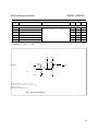
SD Memory Card Slot & Pin-out
Figure 3.5 – SD Memory Card Slot & Pin-out
Two Secure Digital (SD) memory card slots are mounted in the main device. It is
where SD memory cards will be inserted to begin with the operation of the
device and to enable the file management of the SD memory cards through the
mobile phone. The SD card slot has nine interface pins in contact with the SD
33
memory card inserted which are connected to their corresponding data lines to
be processed by the main device circuit.
USB to SD IO host controller bridge chip interface
This chip is used to bridge and process the data lines USB Flash Drive into its
corresponding SD input/output lines. It consists of different components and
integrated circuits such as the USB chip embedded host controller to access
generic USB mass-storage devices; Integrated PCMCIA / CF device designed to
bridge chips using serial or parallel-bit streams; USB transceiver to handle
connection detection functionality as well as providing the analog electrical
signaling required to meet the specification; USB to 16-bit PC Card Interface
Device to enable connection of Compact Flash devices via the USB bus; and
the Field-programmable Gate Array (FPGA) to configure and translate the USB
flash drive into a micro SD-like form.
10uF and 0.1uF Capacitors
A value of 10uF capacitor is used to filter the ripple coming from the regulator so
that a smooth form of supply will be delivered to the microcontroller. Since
microcontroller circuits are designed as direct current (DC) circuits, variations in
the voltages of these circuits can cause problems. If the voltages swing too
much, the circuit may operate incorrectly. For most practical purposes, a voltage
that fluctuates is considered an AC component. The function of the 0.1uF bypass
capacitor is to dampen or isolate the AC, or the electric noise in the circuit.
9V Battery Supply and Standard Battery Connector
34
The device is operated using a 9V battery supply with its connector to make the
device portable.
6V Voltage Regulator
The 9V supply of the device will be regulated into 6V to maintain the voltage
range of the microcontroller’s operating state, which is 5V-6V, and prevent it
from being damaged by a power surge.
Stranded wires
Stranded wires are used in this design to connect the data lines from the
SD memory card slots and the USB bridge chip host interface transfer to the
output data lines which corresponds to the micro SD sniffer. Stranded wires are
used over solid wires because they are flexible and the pins of the data lines are
thin and small enough for that particular wire to fit in.
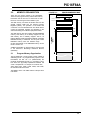
Micro SD Sniffer
Figure 3.6 – micro SD Sniffer
The output of the main device is called the micro SD sniffer. It is a dummy
micro SD card having no memory chip inside and is intended for accessing the
output data lines coming from the SD memory cards and USB flash drive inserted
in the main device. When the selected flash memory has been processed by the
35
device, the memory of the sniffer will be that of the selected flash memory
device and it will be inserted to the mobile phone for file management.
SOFTWARE COMPONENTS
The program for the device is made using C programming language and MikroC
as the program compiler. Pickit2 is utilized to program and debug the
microcontroller.
36
Chapter 4
TESTING, PRESENTATION, AND INTERPRETATION OF DATA
This chapter discusses the testing part of the design; results to those tests can
be found in this part so that it can be determined whether the design is effective
and accurate or not.
Single File Copy Speed Test
The purpose of this is to test if the device is capable of responding efficiently
with the file management features of the mobile phone, specifically the COPY
function of the mobile device. Furthermore, the accuracy of a file when being
transferred from all of the three flash memory devices to the corresponding
memory of the phone is being tested. As indicated in the scope of this study, the
mobile phone model to be used for this purpose is the Nokia C3. The sizes of the
SD Memory Card, mini SD Memory Card and USB Flash Drive are tested based on
the memory size supported by most mobile phone switch is 4 GB of memory.
Another purpose of this test is to determine the causes of errors and data loss in
transferring a file, if there are any. After this test, the functionality of the device
and how successful a single file is transferred without data loss can be
determined. The transfer speed of each file is also measured and observed after
this test.
These are the procedures to be followed in conducting the test:
The COPY function of the mobile phone will be used to duplicate a file from the
given SD memory cards and USB flash drive or vice versa.
37
For each memory type, the maximum memory capacities of the three flash
memories in accordance with the design’s delimitation will be used. For both SD
memory card and mini SD memory card, 4 GB memory size will be used; and for
USB flash drive, 8 GB memory size will also be used.
The file sizes that will be used for testing are 1 MB and 10 MB whose file
types/extensions to be used are .jpg (picture file) and .mp4 (video file)
respectively. Note that these files are supported by the test phone. Separate
tables will be provided for each file size.
Thirty trials will be made to test and observe the consistency of the file transfer
speed.
To make sure that the data transferred is correct and is the same file from the
source, a prompt should be displayed on the mobile phone indicating that the file
has been successfully transmitted. Moreover, the file that has been transferred
should be similar to the source file being copied from in terms of their size in
bytes. If the mobile phone supports the file format of the file being transferred
(e.g., music, documents, pictures), then it should be opened successfully in the
mobile phone. On the other hand, a corrupted icon or image is displayed by the
mobile phone if it is not successful at all.
The results to be displayed in the tables are the transfer speed of the file in
seconds out of 30 trials made. A timer is used to measure the transfer speed of
the file copied from the flash memory to the phone memory in seconds. The
38
average transfer speed computed from the results of the 30 trials is displayed at
another table.
The REMARKS column is intended for the instance of having successful or
unsuccessful file transfers during the actual process, and if the files are
successfully copied only from the external memory to the mobile phone, the
other way around, or both.
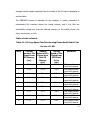
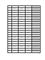
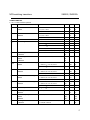
Tables of data collected:
Table 4.1. File Copy Speed Test Results using Phone Model Nokia C3 at
file size of 1 MB
TRIAL
Transfer
Speed of File
Copied from
SD Memory
(sec)
1
3.2 s
Transfer
Speed of File
Copied from
Mini SD
Memory
(sec)
4.3 s
Transfer
Speed of File
Copied from
USB Flash
Drive
(sec)
5.2 s
2
3.2 s
4.3 s
5.3 s
3
3.1 s
4.3 s
5.2 s
4
3.2 s
4.3 s
5.4 s
5
3.2 s
4.5 s
5.4 s
6
3.3 s
4.5 s
5.4 s
7
3.2 s
4.5 s
5.4 s
8
3.2 s
4.5 s
5.4 s
9
3.1 s
4.5 s
5.4 s
REMARKS
File copied to and
from both devices
File copied to and
from both devices
File copied to and
from both devices
File copied to and
from both devices
File copied to and
from both devices
File copied to and
from both devices
File copied to and
from both devices
File copied to and
from both devices
File copied to and
from both devices
39
10
3.2 s
4.5 s
5.4 s
11
3.3 s
4.5 s
5.4 s
12
3.3 s
4.5 s
5.4 s
13
3.3 s
4.3 s
5.4 s
14
3.3 s
4.3 s
5.4 s
15
3.3 s
4.4 s
5.4 s
16
3.2 s
4.5 s
5.4 s
17
3.3 s
4.5 s
5.4 s
18
3.2 s
4.3 s
5.4 s
19
3.2 s
4.4 s
5.4 s
20
3.2 s
4.5 s
5.4 s
21
3.3 s
4.5 s
5.3 s
22
3.3 s
4.4 s
5.4 s
23
3.1 s
4.4 s
5.4 s
24
3.3 s
4.5 s
5.4 s
25
3.2 s
4.4 s
5.3 s
26
3.3 s
4.4 s
5.4 s
27
3.2 s
4.4 s
5.3 s
28
3.3 s
4.4 s
5.4 s
20
3.2 s
4.5 s
5.4 s
30
3.2 s
4.5 s
5.4 s
File copied to and
from both devices
File copied to and
from both devices
File copied to and
from both devices
File copied to and
from both devices
File copied to and
from both devices
File copied to and
from both devices
File copied to and
from both devices
File copied to and
from both devices
File copied to and
from both devices
File copied to and
from both devices
File copied to and
from both devices
File copied to and
from both devices
File copied to and
from both devices
File copied to and
from both devices
File copied to and
from both devices
File copied to and
from both devices
File copied to and
from both devices
File copied to and
from both devices
File copied to and
from both devices
File copied to and
from both devices
File copied to and
from both devices
40
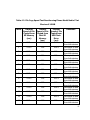
Table 4.2. File Copy Speed Test Results using Phone Model Nokia C3 at
file size of 10 MB
TRIAL
Transfer
Speed of File
Copied from
SD Memory
(sec)
13.2 s
Transfer
Speed of File
Copied from
Mini SD
Memory
(sec)
13.6
Transfer
Speed of File
Copied from
USB Flash
Drive
(sec)
16.5 s
1
2
13.2 s
13.8
16.6 s
3
13.2 s
13.8
16.5 s
4
13.2 s
13.6
16.5 s
5
13.2 s
13.6
16.5 s
6
13.2 s
13.6
16.5 s
7
13.2 s
13.6
16.5 s
8
13.2 s
13.8
16.6 s
9
13.2 s
13.8
16.5 s
10
13.1 s
13.9
16.5 s
11
13.2 s
13.8
16.6 s
12
13.2 s
13.5
16.5 s
13
13.2 s
13.6
16.5 s
14
13.2 s
13.5
16.5 s
REMARKS
File copied to and
from both devices
File copied to and
from both devices
File copied to and
from both devices
File copied to and
from both devices
File copied to and
from both devices
File copied to and
from both devices
File copied to and
from both devices
File copied to and
from both devices
File copied to and
from both devices
File copied to and
from both devices
File copied to and
from both devices
File copied to and
from both devices
File copied to and
from both devices
File copied to and
from both devices
41
15
13.1 s
13.8
16.6 s
16
13.2 s
13.4
16.5 s
17
13.2 s
13.5
16.6 s
18
13.3 s
13.8
16.5 s
19
13.2 s
13.8
16.5 s
20
13.1 s
13.7
16.7 s
21
13.2 s
13.8
16.6 s
22
13.2 s
13.8
16.5 s
23
13.2 s
13.6
16.6 s
24
13.3 s
13.6
16.6 s
25
13.2 s
13.8
16.7 s
26
13.2 s
13.7
16.7 s
27
13.2 s
13.8
16.7 s
28
13.2 s
13.8
16.6 s
20
13.2 s
13.7
16.7 s
30
13.3 s
13.7
16.5 s
File copied to and
from both devices
File copied to and
from both devices
File copied to and
from both devices
File copied to and
from both devices
File copied to and
from both devices
File copied to and
from both devices
File copied to and
from both devices
File copied to and
from both devices
File copied to and
from both devices
File copied to and
from both devices
File copied to and
from both devices
File copied to and
from both devices
File copied to and
from both devices
File copied to and
from both devices
File copied to and
from both devices
File copied to and
from both devices
The average file transfer speed for each flash memory device is computed
using the formula:
+
+
. . . . . . . . . . . +
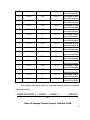
Table 4.3 Average Transfer Speed at 1 MB and 10 MB
42
File Size
Average
Average
Average
Transfer Speed
Transfer Speed
Transfer Speed
in SD Memory
In mini SD
in USB Flash
Card
Memory Card
Drive
1 MB
3.2 s
4.4 s
5.4 s
10 MB
13.2 s
13.7 s
16.6 s
The formula below is used to get the standard deviation for each proportion. This
will determine how much variation or "dispersion" there is from the average
transfer speed of each flash memory with respect to our device.
Where s2 is the variance, X is the speed value per n trial, and N is the number of
trials which is 30. The standard deviation S is simply the square root of variance.
Table 4.4 summarizes the variance and standard deviation of the results
in Tables 4.1 and 4.2.
Table 4.4 Variance and Standard Deviation at 1 MB and 10 MB
Variance
Standard
Deviation
Transfer Speed
in SD Memory
Card
Transfer Speed
In mini SD
Memory Card
Transfer Speed
in USB Flash
Drive
0.004241379
0.065125873
0.006850575
0.082768199
0.003402299
0.058329228
Based on the results gathered in Tables 4.1 and 4.2, the file copy test is
successful for the mobile phone model Nokia C3 to and from SD memory cards
and USB flash drives. It can be implied that the device is capable of copying files
43
of different types and sizes such as 1 MB and 10 MB. The transfer speed is also
measured and was observed to be close to each other.
With regards to the transfer speed of the files copied from the USB flash
drive or SD memory card to the mobile phone, it was observed that the average
transfer rate of the flash memories with respect to the prototype. The actual
transfer speed of the Mini SD Card was lower than the SD Memory card because
the Mini SD card is connected to another adaptor which implies an additional
data rate going to the destination. Nevertheless, since the standard deviation
was smaller than half of the average for all the three flash memories, the results
are said to be consistent which makes device functional and reliable with regards
to the file transfer speed value.
The transfer speed for the USB flash drive to the mobile phone is lower
than the transfer speed of SD memory card and Mini SD memory card. This is
due to the technology of the USB flash drive compared to memory cards which
has larger power dissipation for data transfer.
During the testing process, other file management features of the mobile phone
such as the delete and move options were tested. Therefore it can also be
implied that the file management is successfully operated with the device.
Impact Analysis
The design solution can help in the country’s economic growth when the device
is given a chance to develop further and to become a product which is
manufactured, thus aiding in employing people. The device is also environment44
friendly
because
no
harmful
components
are
used
in
the
hardware
implementation process, which in turn yields to good health and a safe
environment. Although the device has a little problem with its manufacturing
capability because some of the major components are not yet available in the
country, its sustainability is not questionable and it can be offered in the future
where technology is much advanced. The device can have a big impact on social
welfare as it is intended not just for a single person but to all who need it.
45
Chapter 5
CONCLUSION AND RECOMMENDATION
Conclusion
Based on the objectives of the design and the results of test performed
the following observations and conclusions can be made.
The general conclusion is that file integrity is preserved upon
copying/moving between the mobile phone and the device, which hosts the
Secure Digital (SD) card, miniSD card and the USB flash disk.
The following are the specific conclusions:
Developing a design that can transfer data on a variety of media affords a lot of
convenience and flexibility.
Specific lines of circuit are activated for each switch selected, thereby saving
power.
The mobile phone provides the power for the USB flash drive and memory card
slots while the relays are for the selection of lines in the circuit to be activated.
46
Recommendations
The following are recommended ways to improve the design:
While a PIC microcontroller was used in this design, other microcontrollers can
be used as well as long as the requirements for proper operation are satisfied.
The overall power of the circuit can be reduced when using surface mount
components.
Adding another memory card slot can be considered since not all memory cards
can be hosted on the SD card adapter.
Other USB host adapter can be used to support large capacity USB flash drives.
When planning to use the original design, extending its memory card support
can be done be reprogramming the PIC microcontroller.
47
BIBLIOGRAPHY
De Vries, H., De Ruijter, J. and Argam, N (2009). Dominant Design or Multiple
Designs: The Flash Memory Card Case . ERIM Report Series. Reference No. ERS2009-032-LIS
Dorf, R. and Svoboda, J. (2001). Introduction to Electric Circuits (5th ed.). New
York: John Wiley and Sons, Inc.
Huelsman, L. (1972). Basic Circuit Theory with Digital Computations.Series in
computer applications in electrical engineering. Englewood Cliffs: Prentice-Hall.
Maini, K. (1998). Electronic Projects for Beginners, "PustakMahal", 2nd Edition
Millman-Halkias (1972).Integrated Electronics, McGraw-Hill Kogakusha
Matthaei, G., Young,L. and Jones, EMT (1964), Microwave Filters, ImpedanceMatching Networks, and Coupling Structures.McGraw-Hill
Patil, P. and Chitnis, M. (2005). Basic Electricity and Semiconductor
Devices.PhadkePrakashan.
Kuehnel, R. (2009). Circuit Analysis of a Legendary Tube Amplifier: The Fender
Bassman 5F6-A, 3rd Ed., Seattle: Pentode Press.
Rick Gilmour et al., editor, Canadian Electrical Code Part I, Nineteenth Edition,
C22.1-02 Safety Standard for Electrical Installations, Canadian Standards
Association, Toronto, Ontario Canada (2002) ISBN 1-553246-00-X, rule 8-102
Boylestad, R. and Nashelsky, L. (2005). Electronic Devices and Circuit
Theory.Prentice-Hall Career & Technology.
48
Rostky, G. (2002). Remembering the PROM knights of Intel.EE Times.Retrieved
2007-02-08. http://www.eetimes.com/electronics-news/4043577/Rememberingthe-PROM-knights-of-Intel
Ryder, J. (1970). Electronic Fundamentals & Applications, Pitman Publishing
Sedra, A. and Smith, K. (2004). Microelectronic Circuits.Oxford University Press.
Tal, A. (February 2002). NAND vs. NOR flash technology: The designer should
weigh the options when using flash memory. Retrieved 2010-07-31.
http://www2.electronicproducts.com/NAND_vs_NOR_flash_technology-articleFEBMSY1-feb2002-html.aspx
Ulaby, F. (1999 Ed). Fundamentals of Applied Electromagnetics (1999 ed.).
Upper Saddle River, New Jersey: Prentice-Hall.
Viken, A. (2009). The History of Personal Digital Assistants 1980 – 2000. Agile
Mobility.Retrieved February 18, 2011. http://agilemobility.net/2009/04/thehistory-of-personal-digital-assistants1/
Wei K. (2005). 2005 Conference on High Density Microsystem Design and
Packaging and Component Failure Analysis. IEEE Spectrum, 1 – 5
Zorpette, G. (2005). “Super Charged: A Tiny South Korean Company is Out to
Make Capacitors Powerful enough to Propel the Next Generation of HybridElectric Cars.” IEEE Spectrum
49
APPENDICES
APPENDIX A
OPERATION’S MANUAL
System Requirements
Intel Pentium IV or greater
Windows XP, Vista, or Windows 7
MPLAB, ePICKIT2
Mobile phone with Micro SD Slot
Installation Procedure
1. ePICKIT2 installation
Open the PICKit2 v2.61 installer and click ”Next”.
Enter the installation directory and click ”Next”.
Choose “I agree” and click next until the progress bar appears
Wait for it until the PICKit2 has been successfully installed.
Click “Close” when it finishes.
2. MPLAB installation
Open the MPLAB v8.56 setup installer and click ”Next”.
Choose “I accept” and click ”Next”.
Select the complete installation then click ”Next”.
Enter the installation directory and click ”Next”.
Click “Install” and wait until it finishes.
Close the installer when it is successfully installed.
50
III. User’s Manual
How to Setup the Device for File Management of a USB Flash Drive and
SD Memory Card using the Micro SD slot of a Mobile Phone:
Insert the necessary USB flash drive and/or SD memory card in the memory
slot/s of the device. Be sure that the flash memories to be used conform to the
system’s requirements.
Once inserted, the user may now select through push buttons the flash memory
to be read and accessed by the mobile phone with the micro SD slot. The yellow
and blue switches correspond to the activation of SD memory 1 and 2
respectively, while the white switch corresponds to the activation of the USB
flash drive.
If multiple flash memories are inserted, the user may select the order of which
flash memory is to be read first, next and/or last. Multiple switching is allowed in
this case.
Once the selected flash memory is activated, insert the micro SD output sniffer
to the memory slot of the mobile phone.
Go the File Manager section of the mobile phone. If the device is successfully
inserted, the file manager can read and identify the name and free size in bytes
of the corresponding flash memory, aside from its phone memory. For other
phone models, the flash memory should be visible to the Gallery section of the
mobile phone.
51
Open the contents of the flash memory. The user can now browse and manage
the files inside by selecting the specific file and then the Options menu that is
subsequent to the chosen file.
When copying or moving a file from the flash memory to the phone memory or
vice versa, an indication is seen if the file was successfully moved or copied.
When the user is done browsing and accessing the flash memory in the mobile
phone, simply unplug the micro SD sniffer output cable from the phone and turn
off the switch button which corresponds to the flash memory that was read
earlier.
In case the user configured another flash memory to be read by the mobile
phone, just select the button that corresponds to that flash memory and repeat
the above procedures 4 to 8.
IV. Troubleshooting Guides and Procedures
If the device is not responding or operating, check first the battery supply if it is
still operating at a minimum voltage of 5-6 V. If not, change the battery pack
into 9 V.
If the switch indicators are the problem, the LED must just be busted. Replace it
with a new one.
Check the wirings and cables inside and outside the device container if they are
still connected with each other.
If the device output is now connected to the micro SD memory slot of the mobile
phone and the flash memory being activated is not visible or is corrupted in the
52
File Manager or Gallery section of the phone, reinsert the micro SD sniffer onto
the memory slot and try again.
If the flash memory to be read is still not visible or is corrupted, reboot first the
device, reinsert the flash memory onto the memory slot of the device, reinsert
the micro SD sniffer and then try again.
If the file transfer between the flash memory and phone memory is not
successful, reinsert the micro SD sniffer and try again. The pin/s of the micro SD
output may have just not been properly connected to the memory slot of the
mobile phone.
The mobile phone may not be able to read immediately another flash memory
immediately after the preceding flash memory. The user will have to reinsert the
micro SD output sniffer on to the memory slot to refresh the file manager and to
be able to read the current flash memory that is activated.
V. Error Definitions
The light indicators are off when the button is pressed – the power supply is off
or insufficient.
The file management is not successful – the micro SD sniffer is not properly
connected to the mobile phone slot.
53
APPENDIX B
SET OF DATA SHEETS
DESCRIPTION
emitter
base
2N2222; 2N2222A
NPN switching transistors
collector, connected to case
Product specification
Supersedes data of September 1994
File under Discrete Semiconductors, SC04
1997 May 29
54
NPN switching transistors
2N2222; 2N2222A
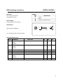
FEATURES
PINNING
DESCRIPTION
High current (max. 800 mA)
emitter
Low voltage (max. 40 V).
base
collector, connected to case
APPLICATIONS
Linear amplification and switching.
DESCRIPTION
3
1
2
PNP complement: 2N2907A.
3
MAM264
1
Fig.1 Simplified outline (TO-18) and symbol.
QUICK REFERENCE DATA
SYMBOL PARAMETER
VCBO
MAX.
UNIT
60
75
V
V
2N2222
30
V
collector-base voltage
CONDITIONS
MIN.
open emitter
2N2222
2N2222A
VCEO
collector-emitter voltage
open base
2N2222A
40
V
IC
collector current (DC)
800
mA
Ptot
total power dissipation
Tamb
500
mW
hFE
fT
DC current gain
IC = 10 mA; VCE = 10 V
transition frequency
IC = 20 mA; VCE = 20 V; f = 100 MHz
25 C
250
2N2222
turn-off time
MHz
300
2N2222A
toff
75
ICon = 150 mA; IBon = 15 mA; IBoff = 15 mA
MHz
250
ns
55
NPN switching transistors
2N2222; 2N2222A
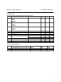
LIMITING VALUES
In accordance with the Absolute Maximum Rating System (IEC 134).
SYMBOL PARAMETER
MAX.
UNIT
2N2222
60
V
2N2222A
75
V
30
V
40
V
2N2222
5
V
2N2222A
6
V
IC
collector current (DC)
800
mA
ICM
peak collector current
800
mA
IBM
peak base current
200
mA
Ptot
total power dissipation
500
mW
1.2
W
Tstg
storage temperature
+150
C
Tj
junction temperature
200
C
Tamb
operating ambient temperature
+150
C
VCBO
VCEO
collector-base voltage
collector-emitter voltage
CONDITIONS
MIN.
open emitter
open base
2N2222
2N2222A
VEBO
emitter-base voltage
open collector
Tamb
25 C
Tcase
25 C
65
65
THERMAL CHARACTERISTICS
SYMBOL
PARAMETER
Rth j-a
thermal resistance from junction to ambient
Rth j-c
thermal resistance from junction to case
CONDITIONS
in free air
VALUE
UNIT
350
K/W
146
K/W
56
NPN switching transistors
2N2222; 2N2222A
CHARACTERISTICS
Tj = 25 C unless otherwise specified.
SYMBOL PARAMETER
ICBO
MIN.
MAX.
UNIT
IE = 0; VCB = 50 V
10
nA
IE = 0; VCB = 50 V; Tamb = 150 C
10
A
IE = 0; VCB = 60 V
10
nA
IE = 0; VCB = 60 V; Tamb = 150 C
10
A
10
nA
collector cut-off current
2N2222
ICBO
CONDITIONS
collector cut-off current
2N2222A
IEBO
emitter cut-off current
IC = 0; VEB = 3 V
hFE
DC current gain
IC = 0.1 mA; VCE = 10 V
35
IC = 1 mA; VCE = 10 V
50
hFE
DC current gain
hFE
DC current gain
IC = 10 mA; VCE = 10 V
75
IC = 150 mA; VCE = 1 V; note 1
50
IC = 150 mA; VCE = 10 V; note 1
100
2N2222A
35
IC = 500 mA; VCE = 10 V; note 1
2N2222
30
40
2N2222A
VCEsat
collector-emitter saturation voltage
2N2222
VCEsat
400
mV
IC = 500 mA; I B = 50 mA; note 1
1.6
V
IC = 150 mA; I B = 15 mA; note 1
300
mV
IC = 500 mA; I B = 50 mA; note 1
1
V
IC = 150 mA; I B = 15 mA; note 1
1.3
V
IC = 500 mA; I B = 50 mA; note 1
2.6
V
1.2
V
base-emitter saturation voltage
2N2222
VBEsat
IC = 150 mA; I B = 15 mA; note 1
collector-emitter saturation voltage
2N2222A
VBEsat
300
IC = 10 mA; VCE = 10 V; Tamb = 55 C
base-emitter saturation voltage
2N2222A
IC = 150 mA; I B = 15 mA; note 1
0.6
IC = 500 mA; I B = 50 mA; note 1
2
V
Cc
collector capacitance
IE = ie = 0; VCB = 10 V; f = 1 MHz
8
pF
Ce
emitter capacitance
IC = ic = 0; VEB = 500 mV; f = 1 MHz
25
pF
2N2222A
fT
transition frequency
IC = 20 mA; VCE = 20 V; f = 100 MHz
2N2222
2N2222A
F
noise figure
2N2222A
IC = 200 A; VCE = 5 V; RS = 2 k ;
f = 1 kHz; B = 200 Hz
250
MHz
300
MHz
4
dB
57
NPN switching transistors
2N2222; 2N2222A
SYMBOL PARAMETER
CONDITIONS
MIN.
MAX.
UNIT
Switching times (between 10% and 90% levels); see Fig.2
ton
td
turn-on time
35
ns
delay time
10
ns
tr
rise time
25
ns
toff
turn-off time
250
ns
ts
storage time
200
ns
tf
fall time
60
ns
ICon = 150 mA; I Bon = 15 mA; IBoff = 15 mA
Note
1. Pulse test: t p
300 s;
0.02.
VBB
RB
Vi
RC
Vo
(probe)
450
oscilloscope
VCC
(probe)
450
oscilloscope
R2
DUT
R1
MLB826
Vi = 9.5 V; T = 500 s; tp = 10 s; t r = tf
3 ns.
R1 = 68 ; R2 = 325 ; RB = 325 ; RC = 160
3.5 V; VCC = 29.5 V.
Oscilloscope input impedance Zi = 50 .
. VBB =
Fig.2 Test circuit for switching
58
M
PIC16F84A
18-pin Enhanced FLASH/EEPROM 8-Bit Microcontroller
High Performance RISC CPU Features:
Pin Diagrams
• Only 35 single word instructions to learn
• All instructions single-cycle except for program
branches which are two-cycle
• Operating speed: DC - 20 MHz clock input
DC - 200 ns instruction cycle
• 1024 words of program memory
• 68 bytes of Data RAM
• 64 bytes of Data EEPROM
• 14-bit wide instruction words
• 8-bit wide data bytes
• 15 Special Function Hardware registers
• Eight-level deep hardware stack
• Direct, indirect and relative addressing modes
• Four interrupt sources:
- External RB0/INT pin
- TMR0 timer overflow
- PORTB<7:4> interrupt-on-change
- Data EEPROM write complete
PDIP, SOIC
1
18
RA1
RA3
RA4/T0CKI
2
3
17
RA0
16
OSC1/CLKIN
MCLR
4
15
OSC2/CLKOUT
VSS
RB0/INT
5
6
14
13
VDD
RB7
RB1
7
12
RB6
RB2
8
11
RB5
RB3
9
10
RB4
SSOP
SS
5
SS
6
RB0/INT
7
8
PIC16F84A
• 13 I/O pins with individual direction control
• High current sink/source for direct LED drive
- 25 mA sink max. per pin
- 25 mA source max. per pin
• TMR0: 8-bit timer/counter with 8-bit
programmable prescaler
• 10,000 erase/write cycles Enhanced FLASH
Program memory typical
• 10,000,000 typical erase/write cycles EEPROM
Data memory typical
• EEPROM Data Retention > 40 years
• In-Circuit Serial Programming™ (ICSP™) - via
two pins
• Power-on Reset (POR), Power-up Timer (PWRT),
Oscillator Start-up Timer (OST)
• Watchdog Timer (WDT) with its own On-Chip RC
Oscillator for reliable operation
• Code protection
• Power saving SLEEP mode
• Selectable oscillator options
MCLR
2
3
4
RA4/T0CKI
Peripheral Features:
Special Microcontroller Features:
PIC16F84A
RA2
OSC1/CLKIN
OSC2/CLKOUT
DD
DD
9
10
CMOS Enhanced FLASH/EEPROM
Technology:
•
•
•
•
-
Low power, high speed technology
Fully static design
Wide operating voltage range:
Commercial: 2.0V to 5.5V
Industrial:
2.0V to 5.5V
Low power consumption:
< 2 mA typical @ 5V, 4 MHz
15 A typical @ 2V, 32 kHz
< 0.5 A typical standby current @ 2V
58
PIC16F84A
1.0
DEVICE OVERVIEW
The program memory contains 1K words, which translates to 1024 instructions, since each 14-bit program
memory word is the same width as each device instruction. The data memory (RAM) contains 68 bytes. Data
EEPROM is 64 bytes.
This document contains device specific information for
the operation of the PIC16F84A device. Additional
information may be found in the PICmicro™ Mid- Range
Reference Manual, (DS33023), which may be
downloaded from the Microchip website. The Reference Manual should be considered a complementary
document to this data sheet, and is highly recommended reading for a better understanding of the device
architecture and operation of the peripheral modules.
There are also 13 I/O pins that are user-configured on
a pin-to-pin basis. Some pins are multiplexed with other
device functions. These functions include:
• External interrupt
• Change on PORTB interrupt
• Timer0 clock input
The PIC16F84A belongs to the mid-range family of the
PICmicro® microcontroller devices. A block diagram of
the device is shown in Figure 1-1.
FIGURE 1-1:
Table 1-1 details the pinout of the device with descriptions and details for each pin.
PIC16F84A BLOCK DIAGRAM
13
Program Counter
Data Bus
8
EEPROM Data Memory
FLASH Program
Memory
8 Level Stack
(13-bit)
1K x 14
Program
Bus
14
EEPROM
EEDATA
RAM
File Registers
68 x 8
7
RAM Addr
Data Memory
64 x 8
EEADR
Addr Mux
Instruction Register
5
7
Direct Addr
TMR0
Indirect
Addr
FSR reg
RA4/T0CKI
STATUS reg
8
MUX
8
Instruction Decode &
Control
Start-up
I/O Ports
ALU
RA3:RA0
Timing
Generation
W reg
RB7:RB1
RB0/INT
59
PIC16F84A
MEMORY ORGANIZATION
There are two memory blocks in the PIC16F84A.
These are the program memory and the data memory.
Each block has its own bus, so that access to each
block can occur during the same oscillator cycle.
The data memory can further be broken down into the
general purpose RAM and the Special Function
Registers (SFRs). The operation of the SFRs that
control the “core” are described here. The SFRs used to
control the peripheral modules are described in the
section discussing each individual peripheral module.
The data memory area also contains the data EEPROM
memory. This memory is not directly mapped into the
data memory, but is indirectly mapped. That is, an
indirect address pointer specifies the address of the data
EEPROM memory to read/write. The 64 bytes of data
EEPROM memory have the address range
0h-3Fh. More details on the EEPROM memory can be
found in Section 3.0.
FIGURE 2-1:
PROGRAM MEMORY MAP
AND STACK - PIC16F84A
PC<12:0>
CALL, RETURN
RETFIE, RETLW
Stack Level 1
13
Stack Level 8
RESET Vector
Peripheral Interrupt Vector
0000h
0004h
User
2.0
Additional information on device memory may be found
in the PICmicro™ Mid-Range Reference Manual,
(DS33023).
3FFh
2.1
Program Memory Organization
The PIC16FXX has a 13-bit program counter capable of
addressing an 8K x 14 program memory space. For the
PIC16F84A, the first 1K x 14 (0000h-03FFh) are
physically implemented (Figure 2-1). Accessing a location above the physically implemented address will
cause a wraparound. For example, for locations 20h,
420h, 820h, C20h, 1020h, 1420h, 1820h, and 1C20h,
the instruction will be the same.
1FFFh
The RESET vector is at 0000h and the interrupt vector
is at 0004h.
60
PIC16F84A
2.2
Data Memory Organization
The data memory is partitioned into two areas. The first
is the Special Function Registers (SFR) area, while the
second is the General Purpose Registers (GPR) area.
The SFRs control the operation of the device.
Portions of data memory are banked. This is for both
the SFR area and the GPR area. The GPR area is
banked to allow greater than 116 bytes of general
purpose RAM. The banked areas of the SFR are for the
registers that control the peripheral functions. Banking
requires the use of control bits for bank selection.
These control bits are located in the STATUS Register.
Figure 2-2 shows the data memory map organization.
Instructions MOVWF and MOVF can move values from
the W register to any location in the register file (“F”),
and vice-versa.
The entire data memory can be accessed either directly
using the absolute address of each register file or
indirectly through the File Select Register (FSR)
(Section 2.5). Indirect addressing uses the present
value of the RP0 bit for access into the banked areas of
data memory.
Data memory is partitioned into two banks which
contain the general purpose registers and the special
function registers. Bank 0 is selected by clearing the
RP0 bit (STATUS<5>). Setting the RP0 bit selects Bank
1. Each Bank extends up to 7Fh (128 bytes). The first
twelve locations of each Bank are reserved for the
Special Function Registers. The remainder are General Purpose Registers, implemented as static RAM.
2.2.1
FILE
FIGURE 2-2:
PIC16F84A
REGISTER FILE MAP -
File Address
00h
01h
File Address
Indirect
TMR0
Indirect
80h
OPTION_REG
81h
02h
82h
STATUS
STATUS
05h
PORTA
TRISA
85h
06h
PORTB
TRISB
86h
08h
EEDATA
EECON1
09h
EEADR
0Ah
PCLATH
PCLATH
8Ah
0Bh
INTCON
INTCON
8Bh
03h
04h
83h
84h
07h
87h
88h
89h
0Ch
8Ch
in Bank
4Fh
50h
CFh
D0h
GENERAL PURPOSE REGISTER
Each General Purpose Register (GPR) is 8-bits wide
and is accessed either directly or indirectly through the
FSR (Section 2.5).
The GPR addresses in Bank 1 are mapped to
addresses in Bank 0. As an example, addressing location 0Ch or 8Ch will access the same GPR.
7Fh
FFh
Bank 0
Bank 1
Unimplemented data memory location, read as ’0’.
Note 1: Not a physical register.
61
PIC16F84A
2.3
Special Function Registers
The special function registers can be classified into two
sets, core and peripheral. Those associated with the
core functions are described in this section. Those
related to the operation of the peripheral features are
described in the section for that specific feature.
The Special Function Registers (Figure 2-2 and
Table 2-1) are used by the CPU and Peripheral
functions to control the device operation. These
registers are static RAM.
TABLE 2-1:
Addr Name
SPECIAL FUNCTION REGISTER FILE SUMMARY
Bit 7
Bit 6
Bit 5
Bit 4
Bit 3
Bit 2
Bit 1
Bit 0
Value on
Power-on
RESET
Details
on page
Bank 0
00h
INDF
Uses contents of FSR to address Data Memory (not a physical register)
01h
TMR0
8-bit Real-Time Clock/Counter
02h
PCL
Low Order 8 bits of the Program Counter (PC)
03h
STATUS(2)
IRP
04h
FSR
Indirect Data Memory Address Pointer 0
05h
PORTA(4)
—
—
—
06h
PORTB(5)
RB7
RB6
RB5
07h
—
08h
EEDATA
EEPROM Data Register
09h
EEADR
EEPROM Address Register
0Ah
PCLATH
—
—
—
0Bh
INTCON
GIE
EEIE
T0IE
RP1
RP0
TO
PD
Z
DC
C
11
xxxx xxxx
20
0000 0000
11
0001 1xxx
8
xxxx xxxx
11
---x xxxx
16
RB0/INT xxxx xxxx
18
RA4/T0CKI RA3
RA2
RA1
RA0
RB4
RB2
RB1
RB3
---- ----
Unimplemented location, read as '0'
—
—
xxxx xxxx 13,14
xxxx xxxx 13,14
Write Buffer for upper 5 bits of the PC (1)
INTE
RBIE
T0IF
INTF
RBIF
---0 0000
11
0000 000x
10
---- ----
11
Bank 1
80h
INDF
81h
OPTION_REG RBPU
82h
PCL
Low order 8 bits of Program Counter (PC)
83h
STATUS (2)
IRP
84h
FSR
Indirect data memory address pointer 0
85h
TRISA
86h
TRISB
87h
—
88h
EECON1
89h
EECON2
Uses Contents of FSR to address Data Memory (not a physical register)
—
INTEDG
RP1
—
T0CS
T0SE
RP0
—
TO
PSA
PD
PS2
Z
PS1
DC
PS0
C
PORTA Data Direction Register
PORTB Data Direction Register
Unimplemented location, read as '0'
—
—
—
EEIF
PCLATH
—
—
—
0Bh
INTCON
GIE
EEIE
T0IE
WRERR
WREN
WR
Write buffer for upper 5 bits of the PC
INTE
9
0000 0000
11
0001 1xxx
8
xxxx xxxx
11
---1 1111
16
1111 1111
18
—
RD
EEPROM Control Register 2 (not a physical register)
0Ah
1111 1111
RBIE
T0IF
(1)
INTF
RBIF
—
---0 x000
13
---- ----
14
---0 0000
11
0000 000x
10
Legend: x = unknown, u = unchanged. - = unimplemented, read as '0', q = value depends on condition
Note 1: The upper byte of the program counter is not directly accessible. PCLATH is a slave register for PC<12:8>. The contents of
PCLATH can be transferred to the upper byte of the program counter, but the contents of PC<12:8> are never trans- ferred to
PCLATH.
2: The TO and PD status bits in the STATUS register are not affected by a MCLR Reset.
3: Other (non power-up) RESETS include: external RESET through MCLR and the Watchdog Timer Reset.
4: On any device RESET, these pins are configured as inputs.
5: This is the value that will be in the port output latch.
61
PIC16F84A
2.3.1
STATUS REGISTER
Note 1: The IRP and RP1 bits (STATUS<7:6>)
are not used by the PIC16F84A and should be
programmed as cleared. Use of these bits as
general purpose R/W bits is NOT recommended,
since this may affect upward compatibility with
future products.
The STATUS register contains the arithmetic status of
the ALU, the RESET status and the bank select bit for
data memory.
As with any register, the STATUS register can be the
destination for any instruction. If the STATUS register is
the destination for an instruction that affects the Z, DC
or C bits, then the write to these three bits is disabled.
These bits are set or cleared according to device logic.
Furthermore, the TO and PD bits are not writable.
Therefore, the result of an instruction with the STATUS
register as destination may be different than intended.
2: The C and DC bits operate as a borrow and
digit borrow out bit, respectively, in subtraction.
See the SUBLW and SUBWF instructions for
examples.
3: When the
STATUS
register
is
the
destination for an instruction that affects the Z, DC
or C bits, then the write to these three bits is
disabled. The specified bit(s) will be updated
according to device logic
For example, CLRF STATUS will clear the upper three
bits and set the Z bit. This leaves the STATUS register
as 000u u1uu (where u = unchanged).
Only the BCF, BSF, SWAPF and MOVWF instructions
should be used to alter the STATUS register (Table 7-2),
because these instructions do not affect any status bit.
REGISTER 2-1:
STATUS REGISTER (ADDRESS 03h, 83h)
R/W-0
IRP
R/W-0
RP1
R/W-0
RP0
R-1
TO
R-1
PD
R/W-x
Z
R/W-x
DC
bit 7
R/W-x
C
bit 0
bit 7-6
Unimplemented: Maintain as ‘0’
bit 5
RP0: Register Bank Select bits (used for direct addressing)
01 = Bank 1 (80h - FFh)
00 = Bank 0 (00h - 7Fh)
bit 4
TO: Time-out bit
1 = After power-up, CLRWDT instruction, or SLEEP instruction
0 = A WDT time-out occurred
bit 3
PD: Power-down bit
1 = After power-up or by the CLRWDT instruction
0 = By execution of the SLEEP instruction
bit 2
Z: Zero bit
1 = The result of an arithmetic or logic operation is zero
0 = The result of an arithmetic or logic operation is not zero
bit 1
DC: Digit carry/borrow bit (ADDWF, ADDLW,SUBLW,SUBWF instructions) (for borrow, the polarity
is reversed)
1 = A carry-out from the 4th low order bit of the result occurred
0 = No carry-out from the 4th low order bit of the result
bit 0
C: Carry/borrow bit (ADDWF, ADDLW,SUBLW,SUBWF instructions) (for borrow, the polarity is
reversed)
1 = A carry-out from the Most Significant bit of the result occurred
0 = No carry-out from the Most Significant bit of the result occurred
Note:
A subtraction is executed by adding the two’s complement of the second operand.
For rotate (RRF, RLF) instructions, this bit is loaded with either the high or low order bit of the source register.
Legend:
R = Readable bit
W = Writable bit
U = Unimplemented bit, read as ‘0’
- n = Value at POR
’1’ = Bit is set
’0’ = Bit is cleared
x = Bit is unknown
63
PIC16F84A
2.3.3
INTCON REGISTER
Note: Interrupt flag bits are set when an interrupt
condition occurs, regardless of the state of its
corresponding enable bit or the global enable bit,
GIE (INTCON<7>).
The INTCON register is a readable and writable register
that contains the various enable bits for all interrupt
sources.
REGISTER 2-3:
INTCON REGISTER (ADDRESS 0Bh, 8Bh)
R/W-0
GIE
R/W-0
EEIE
R/W-0
T0IE
R/W-0
INTE
R/W-0
RBIE
R/W-0
R/W-0
T0IF
INTF
bit 7
R/W-x
RBIF
bit 0
bit 7
GIE: Global Interrupt Enable bit
1 = Enables all unmasked interrupts
0 = Disables all interrupts
bit 6
EEIE: EE Write Complete Interrupt Enable bit
1 = Enables the EE Write Complete interrupts
0 = Disables the EE Write Complete interrupt
bit 5
T0IE: TMR0 Overflow Interrupt Enable bit
1 = Enables the TMR0 interrupt
0 = Disables the TMR0 interrupt
bit 4
INTE: RB0/INT External Interrupt Enable bit
1 = Enables the RB0/INT external interrupt
0 = Disables the RB0/INT external interrupt
bit 3
RBIE: RB Port Change Interrupt Enable bit
1 = Enables the RB port change interrupt
0 = Disables the RB port change interrupt
bit 2
T0IF: TMR0 Overflow Interrupt Flag bit
1 = TMR0 register has overflowed (must be cleared in software)
0 = TMR0 register did not overflow
bit 1
INTF: RB0/INT External Interrupt Flag bit
1 = The RB0/INT external interrupt occurred (must be cleared in software)
0 = The RB0/INT external interrupt did not occur
bit 0
RBIF: RB Port Change Interrupt Flag bit
1 = At least one of the RB7:RB4 pins changed state (must be cleared in software)
0 = None of the RB7:RB4 pins have changed state
Legend:
R = Readable bit
W = Writable bit
U = Unimplemented bit, read as ‘0’
- n = Value at POR
’1’ = Bit is set
’0’ = Bit is cleared
x = Bit is unknown
63
PIC16F84A
2.4
PCL and PCLATH
The program counter (PC) specifies the address of the
instruction to fetch for execution. The PC is 13 bits wide.
The low byte is called the PCL register. This reg- ister is
readable and writable. The high byte is called the PCH
register. This register contains the PC<12:8> bits and is
not directly readable or writable. If the pro- gram
counter (PC) is modified or a conditional test is true, the
instruction requires two cycles. The second cycle is
executed as a NOP. All updates to the PCH reg- ister go
through the PCLATH register.
2.4.1
STACK
The stack allows a combination of up to 8 program calls
and interrupts to occur. The stack contains the return
address from this branch in program execution.
Mid-range devices have an 8 level deep x 13-bit wide
hardware stack. The stack space is not part of either
program or data space and the stack pointer is not
readable or writable. The PC is PUSHed onto the stack
when a CALL instruction is executed or an interrupt
causes a branch. The stack is POPed in the event of a
RETURN, RETLW or a RETFIE instruction execution.
PCLATH is not modified when the stack is PUSHed or
POPed.
After the stack has been PUSHed eight times, the ninth
push overwrites the value that was stored from the first
push. The tenth push overwrites the second push (and
so on).
2.5
Indirect Addressing; INDF and
FSR Registers
The INDF register is not a physical register. Addressing
INDF actually addresses the register whose address is
contained in the FSR register (FSR is a pointer). This is
indirect addressing.
EXAMPLE 2-1:
INDIRECT ADDRESSING
• Register file 05 contains the value 10h
• Register file 06 contains the value 0Ah
• Load the value 05 into the FSR register
• A read of the INDF register will return the value
of 10h
• Increment the value of the FSR register by one
(FSR = 06)
• A read of the INDF register now will return the
value of 0Ah.
Reading INDF itself indirectly (FSR = 0) will produce
00h. Writing to the INDF register indirectly results in a
no-operation (although STATUS bits may be affected).
A simple program to clear RAM locations 20h-2Fh
using indirect addressing is shown in Example 2-2.
EXAMPLE 2-2:
HOW TO CLEAR RAM
USING INDIRECT ADDRESSING
NEXT
movlw
movwf
clrf
incf
btfss
goto
0x20
FSR
INDF
FSR
FSR,4
NEXT
;initialize pointer
;to RAM
;clear INDF register
;inc pointer
;all done?
;NO, clear next
CONTINUE
:
;YES, continue
An effective 9-bit address is obtained by concatenating the 8-bit FSR register and the IRP bit (STATUS<7>), as shown in
Figure 2-3. However, IRP is not used in the PIC16F84A.
63
PIC16F84A
TABLE 6-2:
CAPACITOR SELECTION
FOR CRYSTAL OSCILLATOR
Mode
LP
XT
HS
Note:
Freq
OSC1/C1
OSC2/C2
32 kHz
68 - 100 pF
68 - 100 pF
200 kHz
15 - 33 pF
15 - 33 pF
100 kHz
100 - 150 pF 100 - 150 pF
15 - 33 pF
2 MHz
15 - 33 pF
15 - 33 pF
4 MHz
15 - 33 pF
4 MHz
15 - 33 pF
15 - 33 pF
20 MHz
15 - 33 pF
15 - 33 pF
Higher capacitance increases the stability
of the oscillator, but also increases the
start-up time. These values are for design
guidance only. Rs may be required in HS
mode, as well as XT mode, to avoid overdriving crystals with low drive level specification. Since each crystal has its own
characteristics, the user should consult the
crystal manufacturer for appropriate
values of external components.
For VDD > 4.5V, C1 = C2 30 pF is recommended.
6.2.3
RC OSCILLATOR
For timing insensitive applications, the RC device
option offers additional cost savings. The RC oscillator
frequency is a function of the supply voltage, the
resistor (REXT ) values, capacitor (CEXT) values, and
the operating temperature. In addition to this, the oscillator frequency will vary from unit to unit due to normal
process parameter variation. Furthermore, the
difference in lead frame capacitance between package
types also affects the oscillation frequency, especially
for low CEXT values. The user needs to take into
account variation, due to tolerance of the external
R and C components. Figure 6-3 shows how an R/C
combination is connected to the PIC16F84A.
FIGURE 6-3:
RC OSCILLATOR MODE
VDD
R EXT
OSC1
C EXT
PIC16FXX
VSS
FOSC/4
Recommended values: 5 k
Internal
Clock
OSC2/CLKOUT
R EXT 100 k
CEXT > 20pF
64
PIC16F84A
6.3
RESET
The PIC16F84A differentiates between various kinds
of RESET:
•
•
•
•
•
Power-on Reset (POR)
MCLR during normal operation
MCLR during SLEEP
WDT Reset (during normal operation)
WDT Wake-up (during SLEEP)
Figure 6-4 shows a simplified block diagram of the
On-Chip RESET Circuit. The MCLR Reset path has a
noise filter to ignore small pulses. The electrical specifications state the pulse width requirements for the
MCLR pin.
FIGURE 6-4:
Some registers are not affected in any RESET condition;
their status is unknown on a POR and unchanged in any
other RESET. Most other registers are reset to a “RESET
state” on POR, MCLR or WDT Reset during normal operation and on MCLR during SLEEP. They are not affected
by a WDT Reset during SLEEP, since this RESET is
viewed as the resumption of normal operation.
Table 6-3 gives a description of RESET conditions for
the program counter (PC) and the STATUS register.
Table 6-4 gives a full description of RESET states for all
registers.
The TO and PD bits are set or cleared differently in different RESET situations (Section 6.7). These bits are
used in software to determine the nature of the RESET.
SIMPLIFIED BLOCK DIAGRAM OF ON-CHIP RESET CIRCUIT
External Reset
MCLR
WDT
Module
VDD Rise
Detect
VDD
SLEEP
WDT
Time-out
Reset
S
Power-on Reset
OST/PWRT
OST
10-bit Ripple Counter
R
Chip_Reset
Q
OSC1/
CLKIN
On-Chip
RC Osc(1)
PWRT
10-bit Ripple Counter
See Table 6-5
Enable PWRT
Enable OST
Note 1: This is a separate oscillator from the RC oscillator of the CLKIN pin.
2: See Table 6-5.
TABLE 6-3:
RESET CONDITION FOR PROGRAM COUNTER AND THE STATUS REGISTER
Condition
Program Counter
STATUS Register
Power-on Reset
000h
0001 1xxx
MCLR during normal operation
000h
000u uuuu
MCLR during SLEEP
000h
0001 0uuu
WDT Reset (during normal operation)
000h
0000 1uuu
WDT Wake-up
PC + 1
uuu0 0uuu
Interrupt wake-up from SLEEP
(1)
PC + 1
uuu1 0uuu
Legend: u = unchanged, x = unknown
Note 1: When the wake-up is due to an interrupt and the GIE bit is set, the PC is loaded with the interrupt vector (0004h).
65
PIC16F84A
TABLE 6-4:
Register
RESET CONDITIONS FOR ALL REGISTERS
Address
Power-on Reset
MCLR during:
– normal operation
– SLEEP
WDT Reset during
normal operation
Wake-up from SLEEP:
– through interrupt
– through WDT Time-out
W
—
xxxx xxxx
uuuu uuuu
uuuu uuuu
INDF
00h
---- ----
---- ----
---- ----
TMR0
01h
xxxx xxxx
uuuu uuuu
uuuu uuuu
PCL
02h
0000 0000
0000 0000
PC + 1(2)
STATUS
03h
0001 1xxx
000q quuu(3)
uuuq quuu(3)
FSR
04h
xxxx xxxx
uuuu uuuu
uuuu uuuu
(4)
05h
---x xxxx
---u uuuu
---u uuuu
(5)
PORTB
06h
xxxx xxxx
uuuu uuuu
uuuu uuuu
EEDATA
08h
xxxx xxxx
uuuu uuuu
uuuu uuuu
EEADR
09h
xxxx xxxx
uuuu uuuu
uuuu uuuu
PCLATH
0Ah
---0 0000
---0 0000
---u uuuu
INTCON
0Bh
0000 000x
0000 000u
uuuu uuuu(1)
INDF
80h
---- ----
---- ----
---- ----
OPTION_REG
81h
1111 1111
1111 1111
uuuu uuuu
PCL
82h
0000 0000
0000 0000
PC + 1(2)
STATUS
83h
0001 1xxx
000q quuu(3)
uuuq quuu(3)
FSR
84h
xxxx xxxx
uuuu uuuu
uuuu uuuu
TRISA
85h
---1 1111
---1 1111
---u uuuu
TRISB
86h
1111 1111
1111 1111
uuuu uuuu
EECON1
88h
---0 x000
---0 q000
---0 uuuu
EECON2
89h
---- ----
---- ----
---- ----
PCLATH
8Ah
---0 0000
---0 0000
---u uuuu
INTCON
8Bh
0000 000x
0000 000u
uuuu uuuu(1)
PORTA
Legend: u = unchanged, x = unknown, - = unimplemented bit, read as '0', q = value depends on condition
Note 1: One or more bits in INTCON will be affected (to cause wake-up).
2: When the wake-up is due to an interrupt and the GIE bit is set, the PC is loaded with the interrupt vector
(0004h).
3: Table 6-3 lists the RESET value for each specific condition.
4: On any device RESET, these pins are configured as inputs.
5: This is the value that will be in the port output latch.
66
PIC16F84A
6.4
Power-on Reset (POR)
6.6
Oscillator Start-up Timer (OST)
A Power-on Reset pulse is generated on-chip when VDD
rise is detected (in the range of 1.2V - 1.7V). To take
advantage of the POR, just tie the MCLR pin directly (or
through a resistor) to VDD. This will eliminate external
RC components usually needed to create Power-on
Reset. A minimum rise time for VDD must be met for this
to operate properly. See Electrical Specifications for
details.
The Oscillator Start-up Timer (OST) provides a 1024
oscillator cycle delay (from OSC1 input) after the
PWRT delay ends (Figure 6-6, Figure 6-7, Figure 6-8
and Figure 6-9). This ensures the crystal oscillator or
resonator has started and stabilized.
When the device starts normal operation (exits the
RESET condition), device operating parameters (voltage, frequency, temperature, etc.) must be met to
ensure operation. If these conditions are not met, the
device must be held in RESET until the operating conditions are met.
When VDD rises very slowly, it is possible that the
TPWRT time-out and TOST time-out will expire before
VDD has reached its final value. In this case
(Figure 6-9), an external Power-on Reset circuit may
be necessary (Figure 6-5).
For additional information, refer to Application Note
AN607, "Power-up Trouble Shooting."
FIGURE 6-5:
EXTERNAL POWER-ON
RESET CIRCUIT (FOR SLOW VDD POWERUP)
The POR circuit does not produce an internal RESET
when VDD declines.
6.5
Power-up Timer (PWRT)
The Power-up Timer (PWRT) provides a fixed 72 ms
nominal time-out (TPWRT ) from POR (Figures 6-6
through 6-9). The Power-up Timer operates on an
internal RC oscillator. The chip is kept in RESET as long
as the PWRT is active. The PWRT delay allows the VDD
to rise to an acceptable level (possible exception shown in Figure 6-9).
A configuration bit, PWRTE, can enable/disable the
PWRT. See Register 6-1 for the operation of the
PWRTE bit for a particular device.
The power-up time delay TPWRT will vary from chip to
chip due to VDD, temperature, and process variation.
See DC parameters for details.
The OST time-out (TOST ) is invoked only for XT, LP and
HS modes and only on Power-on Reset or wake-up
from SLEEP.
VDD
VDD
D
R
R1
MCLR
C
PIC16FXX
Note 1: External Power-on Reset circuit is required
only if VDD power-up rate is too slow. The diode D
helps discharge the capacitor quickly when VDD
powers down.
2: R < 40 k
is recommended to make sure that
voltage drop across R does not exceed
0.2V (max leakage current spec on MCLR pin is 5 A).
A larger voltage drop will degrade V IH level on the
MCLR pin.
3: R1 = 100 to 1 k will limit any current flow- ing
into MCLR from external capacitor C, in the event of a
MCLR pin breakdown due to ESD or EOS.
XT, HS, LP
RC
72 ms +
1024TOSC 1024TOSC
1024TOSC
72 ms
—
—
67
PIC16F84A
6.8
Interrupts
6.8.1
The PIC16F84A has 4 sources of interrupt:
•
•
•
•
External interrupt RB0/INT pin
TMR0 overflow interrupt
PORTB change interrupts (pins RB7:RB4)
Data EEPROM write complete interrupt
The interrupt control register (INTCON) records
individual interrupt requests in flag bits. It also contains
the individual and global interrupt enable bits.
The global interrupt enable bit, GIE (INTCON<7>),
enables (if set) all unmasked interrupts or disables (if
cleared) all interrupts. Individual interrupts can be
disabled through their corresponding enable bits in
INTCON register. Bit GIE is cleared on RESET.
The “return from interrupt” instruction, RETFIE, exits
interrupt routine as well as sets the GIE bit, which
re-enables interrupts.
The RB0/INT pin interrupt, the RB port change interrupt
and the TMR0 overflow interrupt flags are contained in
the INTCON register.
When an interrupt is responded to, the GIE bit is
cleared to disable any further interrupt, the return
address is pushed onto the stack and the PC is loaded
with 0004h. For external interrupt events, such as the
RB0/INT pin or PORTB change interrupt, the interrupt
latency will be three to four instruction cycles. The exact
latency depends when the interrupt event occurs. The
latency is the same for both one and two cycle
instructions. Once in the Interrupt Service Routine, the
source(s) of the interrupt can be determined by polling
the interrupt flag bits. The interrupt flag bit(s) must be
cleared in software before re-enabling interrupts to
avoid infinite interrupt requests.
Note:
Individual interrupt flag bits are set
regardless of
the statusof
their
corresponding mask bit or the GIE bit.
FIGURE 6-10:
INT INTERRUPT
External interrupt on RB0/INT pin is edge triggered:
either rising if INTEDG bit (OPTION_REG<6>) is set,
or falling if INTEDG bit is clear. When a valid edge
appears on the RB0/INT pin, the INTF bit
(INTCON<1>) is set. This interrupt can be disabled by
clearing control bit INTE (INTCON<4>). Flag bit INTF
must be cleared in software via the Interrupt Service
Routine before re-enabling this interrupt. The INT
interrupt can wake the processor from SLEEP
(Section 6.11) only if the INTE bit was set prior to going
into SLEEP. The status of the GIE bit decides whether
the processor branches to the interrupt vector
following wake-up.
6.8.2
TMR0 INTERRUPT
An overflow (FFh 00h) in TMR0 will set flag bit T0IF
(INTCON<2>). The interrupt can be enabled/disabled
by setting/clearing enable bit T0IE (INTCON<5>)
(Section 5.0).
6.8.3
PORTB INTERRUPT
An input change on PORTB<7:4> sets flag bit RBIF
(INTCON<0>). The interrupt can be enabled/disabled
by setting/clearing enable bit RBIE (INTCON<3>)
(Section 4.2).
Note:
For a change on the I/O pin to be
recognized, the pulse width must be at least TCY
wide.
6.8.4
DATA EEPROM INTERRUPT
At the completion of a data EEPROM write cycle, flag
bit EEIF (EECON1<4>) will be set. The interrupt can be
enabled/disabled by setting/clearing enable bit EEIE
(INTCON<6>) (Section 3.0).
INTERRUPT LOGIC
Wake-up
(If in SLEEP mode)
T0IF
T0IE
INTF
INTE
Interrupt to CPU
RBIF
RBIE
EEIF
EEIE
GIE
2001 Microchip Technology Inc.
DS35007B-page 29
PIC16F84A
6.9
Context Saving During Interrupts
During an interrupt, only the return PC value is saved on
the stack. Typically, users wish to save key register
values during an interrupt (e.g., W register and STATUS
register). This is implemented in software.
The code in Example 6-1 stores and restores the
STATUS and W register’s values. The user defined
registers, W_TEMP and STATUS_TEMP are the temporary storage locations for the W and STATUS
registers values.
EXAMPLE 6-1:
PUSH
ISR
POP
MOVWF
SWAPF
SWAPF
6.10
Example 6-1 does the following:
a) Stores the W register.
b) Stores the STATUS register in STATUS_TEMP.
c) Executes the Interrupt Service Routine code.
d) Restores the STATUS (and bank select bit)
register.
e) Restores the W register.
SAVING STATUS AND W REGISTERS IN RAM
MOVWF
W_TEMP
; Copy W to TEMP register,
SWAPF
STATUS,
W
; Swap status to be saved into W
MOVWF
STATUS_TEMP
; Save status to STATUS_TEMP register
:
:
:
; Interrupt Service Routine
:
; should configure Bank as required
:
;
SWAPF
STATUS_TEMP,W
; Swap nibbles in STATUS_TEMP register
; and place result into W
STATUS
; Move W into STATUS register
; (sets bank to original state)
W_TEMP,
F
; Swap nibbles in W_TEMP and place result in W_TEMP
W_TEMP,
W
; Swap nibbles in W_TEMP and place result into W
Watchdog Timer (WDT)
The Watchdog Timer is a free running On-Chip RC
Oscillator which does not require any external
components. This RC oscillator is separate from the RC
oscillator of the OSC1/CLKIN pin. That means that the
WDT will run even if the clock on the OSC1/CLKIN and
OSC2/CLKOUT pins of the device has been stopped,
for example, by execution of a SLEEP instruction.
During normal operation, a WDT time-out generates a
device RESET. If the device is in SLEEP mode, a WDT
wake-up causes the device to wake-up and continue
with normal operation. The WDT can be permanently
disabled by programming configuration bit WDTE as a '0'
(Section 6.1).
6.10.1
WDT PERIOD
The WDT has a nominal time-out period of 18 ms, (with
no prescaler). The time-out periods vary with
temperature, VDD and process variations from part to
part (see DC specs). If longer time-out periods are
desired, a prescaler with a division ratio of up to 1:128
can be assigned to the WDT under software control by
writing to the OPTION_REG register. Thus, time-out
periods up to 2.3 seconds can be realized.
The CLRWDT and SLEEP instructions clear the WDT
and the postscaler (if assigned to the WDT) and prevent it from timing out and generating a device
RESET condition.
The TO bit in the STATUS register will be cleared upon
a WDT time-out.
69
PIC16F84A
6.10.2
WDT PROGRAMMING
CONSIDERATIONS
It should also be taken into account that under worst
case conditions (VDD = Min., Temperature = Max., Max.
WDT Prescaler), it may take several seconds before a
WDT time-out occurs.
FIGURE 6-11:
WATCHDOG TIMER BLOCK DIAGRAM
From TMR0 Clock Source
(Figure 5-2)
0
WDT Timer
•
M
1
Postscaler
U
8
X
PS2:PS0
8 - to -1 MUX
PSA
WDT Enable Bit
•
To TMR0 (Figure 5-2)
1
0
MUX
PSA
WDT Time-out
Note:
PSA and PS2:PS0 are bits in the OPTION_REG register.
TABLE 6-7:
Addr
Name
2007h Config. bits
81h
SUMMARY OF REGISTERS ASSOCIATED WITH THE WATCHDOG TIMER
Bit 7
Bit 6
Bit 5
Bit 4
(2)
(2)
(2)
(2)
OPTION_REG RBPU
INTEDG T0CS
T0SE
Bit 3
Bit 2
Bit 1
Bit 0
PWRTE(1) WDTE
FOSC1
FOSC0
PSA
PS1
PS0
PS2
Value on
Power-on
Reset
Value on all
other
RESETS
(2)
1111 1111 1111 1111
Legend: x = unknown. Shaded cells are not used by the WDT.
Note 1: See Register 6-1 for operation of the PWRTE bit.
2: See Register 6-1 and Section 6.12 for operation of the code and data protection bits.
70
PIC16F84A
6.11
Power-down Mode (SLEEP)
6.11.2
A device may be powered down (SLEEP) and later
powered up (wake-up from SLEEP).
6.11.1
The device can wake-up from SLEEP through one of
the following events:
1. External RESET input on MCLR pin.
2. WDT wake-up (if WDT was enabled).
3. Interrupt from RB0/INT pin, RB port change, or
data EEPROM write complete.
SLEEP
The Power-down mode is entered by executing the
SLEEP instruction.
If enabled, the Watchdog Timer is cleared (but keeps
running), the PD bit (STATUS<3>) is cleared, the TO bit
(STATUS<4>) is set, and the oscillator driver is turned
off. The I/O ports maintain the status they had before
the SLEEP instruction was executed (driving high, low,
or hi-impedance).
For the lowest current consumption in SLEEP mode,
place all I/O pins at either VDD or VSS, with no external
circuitry drawing current from the I/O pins, and disable
external clocks. I/O pins that are hi-impedance inputs
should be pulled high or low externally to avoid switching currents caused by floating inputs. The T0CKI input
should also be at VDD or VSS. The contribution from
on-chip pull-ups on PORTB should be considered.
The MCLR pin must be at a logic high level (VIHMC).
It should be noted that a RESET generated by a WDT
time-out does not drive the MCLR pin low.
FIGURE 6-12:
WAKE-UP FROM SLEEP
Peripherals cannot generate interrupts during SLEEP,
since no on-chip Q clocks are present.
The first event (MCLR Reset) will cause a device
RESET. The two latter events are considered a continuation of program execution. The TO and PD bits can
be used to determine the cause of a device RESET.
The PD bit, which is set on power-up, is cleared when
SLEEP is invoked. The TO bit is cleared if a WDT
time-out occurred (and caused wake-up).
While the SLEEP instruction is being executed, the next
instruction (PC + 1) is pre-fetched. For the device to
wake-up through an interrupt event, the corresponding
interrupt enable bit must be set (enabled). Wake-up
occurs regardless of the state of the GIE bit. If the GIE
bit is clear (disabled), the device continues execution at
the instruction after the SLEEP instruction. If the GIE bit
is set (enabled), the device executes the instruction
after the SLEEP instruction and then branches to the
interrupt address (0004h). In cases where the
execution of the instruction following SLEEP is not
desirable, the user should have a NOP after the
SLEEP instruction.
WAKE-UP FROM SLEEP THROUGH INTERRUPT
Q1 Q2 Q3 Q4 Q1 Q2 Q3 Q4 Q1
Q1 Q2 Q3 Q4 Q1 Q2 Q3 Q4 Q1 Q2 Q3 Q4 Q1 Q2 Q3 Q4
OSC1
(2) OST
CLKOUT(4)
T
INT pin
INTF Flag
(INTCON<1>)
GIE bit
(INTCON<7>)
Interrupt Latency
(Note 2)
Processor in
SLEEP
INSTRUCTION FLOW
PC
Instruc
Fetc
Instruc
Execu
tion
hed Inst(PC) = SLEEP
tion
Inst(PC - 1)
ted
PC+1
PC+2
PC+2
Inst(PC + 1)
Inst(PC + 2)
SLEEP
Inst(PC + 1)
PC + 2
Dummy cycle
0004h
0005h
Inst(0004h)
Inst(0005h)
Dummy cycle
Inst(0004h)
Note 1: XT, HS, or LP oscillator mode assumed.
2: TOST = 1024TOSC (drawing not to scale). This delay will not be there for RC osc mode.
3: GIE = ’1’ assumed. In this case after wake-up, the processor jumps to the interrupt routine. If GIE = ’0’, execution will continue in-line.
4: CLKOUT is not available in these osc modes, but shown here for timing reference.
71
PIC16F84A
BTFSC
Bit Test, Skip if Clear
CLRWDT
Clear Watchdog Timer
Syntax:
[label] BTFSC f,b
Syntax:
[ label ] CLRWDT
0
Operands:
None
Operation:
0
1
1
00h
PD
Status Affected:
TO, PD
Operands:
0
b
f
127
7
Operation:
skip if (f<b>) = 0
Status Affected:
None
Description:
If bit ’b’ in register ’f’ is ’1’, the next
instruction is executed.
If bit ’b’ in register ’f’ is ’0’, the next
instruction is discarded, and a NOP
is executed instead, making this a
2TCY instruction.
CALL
Call Subroutine
Syntax:
[ label ] CALL k
Operands:
0
Operation:
k
(PCLATH<4:3>)
(PC)+ 1 TOS,
PC<10:0>,
PC<12:11>
Status Affected:
None
k
2047
Description:
Call Subroutine. First, return
address (PC+1) is pushed onto the stack. The elevenbit immedi- ate address is loaded into PC bits
<10:0>. The upper bits of the PC
are loaded from PCLATH. CALL is a two-cycle
instruction.
Description:
CLRWDT instruction resets the
Watchdog Timer. It also resets the prescaler of the
WDT. Status bits TO and PD are set.
COMF
Complement f
Syntax:
[ label ] COMF
Operands:
d
0 f
[0,1]
Operation:
(f)
Status Affected:
Z
(destination)
Description:
The contents of register ’f’ are
complemented. If ’d’ is 0, the result is stored in W. If
’d’ is 1, the result is stored back in register ’f’.
Decrement f
Syntax:
[label] DECF f,d
127
Operands:
d
0 f
[0,1]
(f)
Operation:
(f) - 1
Status Affected:
Z
Clear f
Syntax:
[label] CLRF
Operands:
0
Operation:
1
00h
Z
Status Affected:
Z
f
Description:
The contents of register ’f’ are
cleared and the Z bit is set.
CLRW
Clear W
Syntax:
[ label ] CLRW
Operands:
None
Operation:
1
00h
Z
Status Affected:
Z
Description:
is set.
W register is cleared. Zero bit (Z)
f,d
127
DECF
CLRF
f
WDT
WDT prescaler,
TO
127
(destination)
Description:
Decrement register ’f’. If ’d’ is 0,
the result is stored in the W regis- ter. If ’d’ is 1, the
result is stored back in register ’f’.
(W)
75
PIC16F84A
DECFSZ
Decrement f, Skip if 0
INCFSZ
Increment f, Skip if 0
Syntax:
[ label ] DECFSZ f,d
Syntax:
[ label ]
Operands:
d
0 f
[0,1]
Operands:
d
0 f
[0,1]
Operation:
skip if result = 0
(f) - 1
Operation:
skip if result = 0
(f) + 1
Status Affected:
None
Status Affected:
None
127
(destination);
Description:
The contents of register ’f’ are
decremented. If ’d’ is 0, the result is placed in the W
register. If ’d’ is
1, the result is placed back in register ’f’.
If the result is 1, the next instruc- tion is executed. If
the result is 0, then a NOP is executed instead,
making it a 2TCY instruction.
GOTO
Unconditional Branch
Syntax:
[ label ]
Operands:
0
Operation:
PCLATH<4:3>
k PC<10:0>
PC<12:11> Status Affected:
k
GOTO k
2047
None
Description:
GOTO is an unconditional branch.
The eleven-bit immediate value is
loaded into PC bits <10:0>. The upper bits of PC are
loaded from PCLATH<4:3>. GOTO is a two- cycle
instruction.
INCF
Increment f
Syntax:
[ label ]
Operands:
d
0 f
[0,1]
Operation:
(f) + 1
Status Affected:
Z
INCF f,d
127
(destination)
Description:
The contents of register ’f’ are
incremented. If ’d’ is 0, the result is placed in the W
register. If ’d’ is
1, the result is placed back in
register ’f’.
INCFSZ f,d
127
(destination),
Description:
The contents of register ’f’ are
incremented. If ’d’ is 0, the result is placed in the W
register. If ’d’ is 1, the result is placed back in
register ’f’.
If the result is 1, the next instruc- tion is executed. If
the result is 0,
a NOP is executed instead, making
it a 2TCY instruction.
IORLW
Inclusive OR Literal with W
Syntax:
[ label ]
Operands:
0
k
IORLW k
255
Operation:
(W) .OR. k
Status Affected:
Z
(W)
Description:
The contents of the W register are
OR’ed with the eight-bit literal 'k'. The result is placed
in the W register.
IORWF
Inclusive OR W with f
Syntax:
[ label ]
Operands:
d
0 f
[0,1]
Operation:
(W) .OR. (f)
Status Affected:
Z
IORWF
f,d
127
(destination)
Description:
Inclusive OR the W register with
register 'f'. If 'd' is 0, the result is placed in the W
register. If 'd' is 1, the result is placed back in
register 'f'.
75
PIC16F84A
MOVF
Move f
Syntax:
[ label ]
Operands:
d
0 f
[0,1]
Operation:
(f)
Status Affected:
Z
MOVF f,d
127
(destination)
RETFIE
Return from Interrupt
Syntax:
[ label ]
Operands:
None
Operation:
1
TOS
GIE
Status Affected:
None
RETLW
Return with Literal in W
Syntax:
[ label ]
Operands:
0
Operation:
TOS
k
(W);
PC Status
Affected:
None
RETFIE
PC,
Description:
The contents of register f are
moved to a destination dependant upon the status of d.
If d = 0, des- tination is W register. If d = 1, the
destination is file register f itself.
d = 1 is useful to test a file register,
since status flag Z is affected.
MOVLW
Move Literal to W
Syntax:
[ label ]
Operands:
0
Operation:
k
Status Affected:
None
k
MOVLW k
255
(W)
Description:
The eight-bit literal ’k’ is loaded
into W register. The don’t cares will assemble as 0’s.
k
RETLW k
255
Description:
The W register is loaded with the
eight-bit literal 'k'. The program counter is loaded
from the top of the stack (the return address). This
is a two-cycle instruction.
MOVWF
Move W to f
Syntax:
[ label ]
Operands:
0
Operation:
(W)
Status Affected:
RETURN
Return from Subroutine
Syntax:
[ label ]
Operands:
None
None
Operation:
TOS
Description:
register 'f'.
Move data from W register to
Status Affected:
None
NOP
No Operation
Syntax:
[ label ]
Operands:
None
Operation:
No operation
Status Affected:
None
Description:
No operation.
f
MOVWF
f
127
(f)
RETURN
PC
Description:
Return from subroutine. The stack
is POPed and the top of the stack (TOS) is loaded
into the program counter. This is a two-cycle
instruction.
NOP
77
PIC16F84A
RLF
Rotate Left f through Carry
SUBLW
Subtract W from Literal
Syntax:
[ label ] RLF
Syntax:
[ label ] SUBLW k
Operands:
d
0 f
[0,1]
Operands:
0
Operation:
k - (W)
Operation:
See description below
Status Affected: C, DC, Z
Status Affected:
C
Description:
The W register is subtracted (2’s
complement method) from the eight-bit literal 'k'.
The result is placed in the W register.
f,d
127
Description:
The contents of register ’f’ are
rotated one bit to the left through the Carry Flag. If ’d’
is 0, the result is placed in the W register. If ’d’ is 1, the
result is stored back in register ’f’.
C
k
255
W)
Register f
RRF
Rotate Right f through Carry
SUBWF
Subtract W from f
Syntax:
[ label ]
Syntax:
[ label ] SUBWF f,d
Operands:
d
0 f
[0,1]
Operands:
d
0 f
[0,1]
Operation:
See description below
Operation:
(f) - (W)
Status Affected:
C
Status Affected: C, DC, Z
RRF f,d
127
Description:
The contents of register ’f’ are
rotated one bit to the right through the Carry Flag. If ’d’
is 0, the result is placed in the W register. If ’d’ is
1, the result is placed back in register ’f’.
C
127
destination)
Description:
Subtract (2’s complement method)
W register from register 'f'. If 'd' is 0, the result is
stored in the W regis- ter. If 'd' is 1, the result is
stored back in register 'f'.
Register f
SLEEP
SWAPF
Swap Nibbles in f
Syntax:
[ label ] SLEEP
Syntax:
[ label ] SWAPF f,d
Operands:
None
Operation:
0
1
0
00h
Operands:
d
0 f
[0,1]
Operation:
(f<7:4>)
(f<3:0>)
(destination<7:4>),
(destination<3:0>)
PD
Status Affected:
None
Status Affected:
TO, PD
Description:
The upper and lower nibbles of
register 'f' are exchanged. If 'd' is
0, the result is placed in W regis- ter. If 'd' is 1, the
result is placed in register 'f'.
WDT,
WDT prescaler,
TO,
Description:
The power-down status bit, PD is
cleared. Time-out status bit, TO
is set. Watchdog Timer and its prescaler are
cleared.
The processor is put into SLEEP
mode with the oscillator stopped.
127
77
PIC16F84A
XORLW
Exclusive OR Literal with W
XORWF
Exclusive OR W with f
Syntax:
[label]
Syntax:
[label]
Operands:
0
Operands:
d
0 f
[0,1]
Operation:
(W) .XOR. (f)
Status Affected:
Z
k
XORLW k
255
Operation:
(W) .XOR. k
Status Affected:
Z
W)
Description:
The contents of the W register
are XOR’ed with the eight-bit lit- eral 'k'. The result is
placed in the W register.
2001 Microchip Technology Inc.
XORWF
f,d
127
destination)
Description:
Exclusive OR the contents of the
W register with register 'f'. If 'd' is
0, the result is stored in the W register. If 'd' is 1,
the result is stored back in register 'f'.
DS35007B-page 43
77
Features
Optimised for high speed transfer of data.
USB 2.0 Hi-Speed connection.
- up to 480 Mbps data rate
●
Backward compatibility with Full-Speed
USB 2.0 and USB 1.1.
●
Integrated USB 2.0 Hi-Speed PHY.
●
USB suspend/resume supported
●
3.3V supply.
●
Low power < 600mW operating, <900uA
suspend.
- Suitable for bus powered applications.
●
16 kB USB buffer memory.
●
SDIO interface supports
- 1bit or 4bit SDIO
- SD Interrupt.
●
Card detection.
●
VUB300 live on power up.
●
SD Specifications Part 1 Physical Layer
Specification Version 2.00.
●
SD Specifications Part E1 SDIO Specification Version 2.00.
●
Single chip solution
●
Development / Demonstration board available same functionality with multi
chip solution.
●
Package : 36-pin QFN 6x6mm
●
Fully 'green', lead-free and RoHS
compliant.
●
>120Mbps “Real World” block read/write performance*
●
●
* Read/write performance based on CMD18/25/53 multi-block transfers
79
Introduction
Extending the capabilities of SD and SDIO devices into the world of USB, and also allowing
expansion of Laptop and Desktop PC's into the world of SD and SDIO devices, the VUB300
is a USB to SDIO host controller bridge chip interface that allows SDIO and SD compliant
devices to be connected to any host PC via the Universal Serial Bus (USB). It is a USB 2.0
compliant device operating at Hi-Speed (480 Mbps). The SDIO Host function conforms to
the SDIO Host specification with a generic USB “wrapped” interface to extend SDIO host
controller support to the USB bus.
Device Support
The VUB300 conforms to the SD Specifications Part 1 Physical Layer Specification Version
2.00 and SD Specifications Part E1 SDIO Specification Version 2.00. The VUB300 supports
any SD or SDIO device that conforms to the SD/SDIO specifications.
Host Support
The VUB300 conforms to the USB 2.0 Specification; it is a Hi-Speed device and will work
on any host that supports USB 2.0 or 1.1 host ports. Please note that maximum data
throughput is only available with USB 2.0 Hi-Speed hosts.
80
Operating System Support
The VUB300 SDIO host controller drivers are supported on the following operating
systems:
●
●
●
●
●
●
●
Linux
Windows 2000
Windows XP
Windows Vista 32
Windows Vista 64
Windows Mobile/PocketPC/CE*
Apple MAC OSX*
The drivers integrate with the generic SDIO host stack providing seamless functionality
with existing SD and SDIO device drivers.
*Planned
Functionality and Design
VUB300 offers a unique USB to SDIO host controller interface link with this single chip
bridge solution in the form of an ASIC.
VUB300 offers capability and intelligence to handle both USB and SDIO protocol, creating
the connection between the two and seemingly translating the data between the two
formats.
81
Diagram 3: VUB300 Block Diagram
USB
Integrated USB 2.0 Hi-Speed Transceiver / PHY
VUB300 ASIC has integrated USB 2.0 compliant Hi-Speed Transceiver.
SDIO
SDIO Host Controller, SDIO Host Controller Register and DMA Control, all make up the
SDIO Function Controller section within VUB300, see Diagram 3.
DMA Control
By implementing DMA control VUB300 is able to achieve high performance data transfers
between an SD/SDIO data path and the USB bulk data interface. SD/SDIO blocks transfers
in DMA mode of 256, 512, 1024 and 2048 are supported. Tested and recommended are
256 or 512 block transfers.
SDIO Host Controller
SDIO Function Controller is designed according to the SD Association's SD host controller
specification.
82
SDIO Host Controller Interface
All the access to the SD/SDIO bus are made via the SDIO host transaction processor
accessing the internal SDIO Host controller registers. DMA, burst access, CRC error
detection, SD interrupt, timing, etc. are supported by the transaction processor core.
SD
command and data transfers are initiated by the host side driver as USB transactions,
these are translated into SD bus commands and data transfers. The complete responses
are returned to the host side driver.
VUB300 Bridging Logic
VUB300 has IP core with device specific logic that is adapting, organising and translating
data between USB and SDIO interface. This device specific logic design has been
improved by the Elan development team for superior and fast performance.
83
Pin Descriptions
SECURE DIGITAL INTERFACE
Pin #
Name
Type
Description
23
25
4
5
SD_D[3:0]
SD Data
This is a bi-directional bus that connects to the DAT bus of
SD device
9
SD_CLK
SD Clock
This is an output clock signal to SD/SDIO device
11
SD_CMD
SD Command This is a bi-directional signal that connects to the CMD
signal of SD device
30
SD_WP
SD Write
Protect
This is an IO pin designated as the Secure Digital card
mechanical write protect pin
26
SD_nCD
SD Card
Detect
This is an IO pin designated as the Secure Digital card
detection pin
Description
USB INTERFACE
Pin #
Name
Type
2
3
USB+
USB-
USB Bus Data These pins connect to the USB data bus signals
35
RBIAS
USB
Transceiver
Bias
33
XTAL1
(CLKIN)
24MHz Crystal This pin can be connected to one terminal of the crystal or
or external
it can be connected to an external 24 clock when a crystal
clock input
is not used
32
XTAL2
24MHz
Crystal
This is the other terminal of the crystal, or it is left open
when an external clock source is used to drive
XTAL1(CLKIN). It may not be used to drive any external
circuitry other than the crystal circuit
36
VDDA33
3.3V Analog
Power
3.3V Analog Power
34
VDD18PLL
1.8V PLL
Power
This pin in the 1.8V Power for the PLL
+1.8V Filtered analog power for internal PLL. This pin
must have a 1.0 µF (or greater) ±20% (ESR <0.1Ω)
capacitor to VSS
A 12.0k, 1.0% resistor is attached from VSS to this pin in
order to set the transceiver's internal bias currents
84
MISC
Pin #
Name
Type
Description
1
LED1
General
Purpose IO
This pin may be used to drive an activity LED
21
CRD_PWR
General
Purpose I/O
Card Power drive of 3.3V at either 100mA or 200mA
18
nRESET
RESET Input
This active low signal is used by the system to reset the
chip. The active low pulse should be at least 1µs wide
DIGIGAL / POWER
Pin #
Name
Type
Description
13
VDD18
+1.8V Core
power
+1.8V core power. This pin must have a+1.0 µF (or
greater) ±20% (ESR <0.1Ω) capacitor to VSS
6
13
22
VDD33
3.3V Power & 3.3V power supply input
Regulator
Input
28
TEST
Input
SLUG
VSS
This signal is used for testing the chip. When unused tie to
VSS
Ground reference
85
SDIO Socket Pin Definitions
Pin
Name
Description
1
SD_DAT[3]/CD
Data line 3 / Card detect
2
SD_CMD
Command line
3
VSS1
Ground
4
SD_PWR
Supply voltage, should be connected to CRD_PWR
5
SD_CLK
Clock
6
VSS2
Ground
7
SD_DAT[0]
Data line 0
8
SD_DAT[1]/IRQ
Data line 1 / SDIO Interrupt
9
SD_DAT[2]/WAIT
Data line 2 / SDIO Read Wait
10
SD_nCD
SD/SDIO card detect switch, active LOW
11
SD_WP
SD card write protect switch, active HIGH
86
Reference Design
The following schematic provides USB SD/SDIO card reader reference design.
VUB300 main block
87
Power supply block
Clock reference block
SD/SDIO socket block
88
USB socket block
89
Symbol
Min
A
'0.80
A1
A2
0
Max
5.85
D1/E1
5.55
D2/E2
'4.00
L
b
'6.00
Notes
'1.00
Overall package height
0.05
Standoff
'0.80
Mold cap thickness
0.20 REF
D/E
x
0.02
'0.60
A3
e
Nom
Leadframe thickness
'6.15
X/Y body size
5.95
X/Y mold cap size
'4.10
'4.20
X/Y exposed pad size
'0.50
'0.60
'0.75
Terminal length
0.18
0.25
'0.30
Terminal width
0.50 BSC
Terminal pitch
4 X 0° - 12°
90
Electrical Specifications
Parameter
Conditions
Supply Voltage (VDD)
Operating Temperature Range
Min
3.0
Industrial
Typ
3.3
-40
Max
3.6
+85
Units
V
°C
Full Speed IDD
110
140
mA
High Speed IDD
135
165
mA
Supply current USB suspend
350
900
uA
Recommended Operating Conditions
Parameter
Min
Max
Units
Operating Temperature
-40
85
°C
3.3V Supply Voltage (VDD33, VDDA33)
'3.0
3.6
°C
3.3V Supply rise time
0
400
°C
Voltage on USB+ and USB- pins
-0.3
5.5
V
Voltage on any signal pin
-0.3
VDD33
V
Voltage on XTAL1
-0.3
VDDA33
V
Voltage on XTAL2
-0.3
VDD18
V
91
Absolute Maximum Ratings*
Parameter
Min
Max
Units
Ambient temperature under bias
-55
125
°C
Storage Temperature
-65
150
°C
Lead Temperature
325
(soldering < 10 seconds)
'4.0
°C
3.3V supply voltage (V DD33, VDDA33 )
-0.5
Voltage on USB+ and USB- pins
-0.5
Voltage on CRD_PWR
-0.5
VDD33 + 0.3
V
Voltage on any signal pin
-0.5
VDD33 + 0.3
V
Voltage on XTAL1
-0.5
(3.3V supply voltage + 2) ≤ 6
'4.0
V
V
V
Voltage on XTAL2
-0.5
VDD18 + 0.3
V
*Note: Stresses above those listed under “Absolute Maximum Ratings” may cause permanent
damage to the device. This is a stress rating only and functional operation of the devices at those
or any other conditions above those indicated in the operation listings of this specification is not
implied. Exposure to maximum rating conditions for extended periods may affect device reliability.
92
APPENDIX C
PROGRAM LISTING
void main()
{
TRISB = 0x07;
PORTB = 0;
while(1){
while(PORTB.F0 == 1){
PORTB.F3 = 1;
PORTB.F4 = 0;
PORTB.F5 = 0;
}
while(PORTB.F1 == 1){
PORTB.F4 = 1;
PORTB.F5 = 0;
PORTB.F3 = 0;
}
while(PORTB.F2 == 1)
100
{
PORTB.F5 = 1;
PORTB.F3 = 0;
PORTB.F4 = 0;
}
PORTB.F3 = 0;
PORTB.F4 = 0;
PORTB.F5 = 0;
}
}
101
APPENDIX D
PICTURES OF PROTOTYPE
PCB Layout
Final Circuit Design of the Device
102
Prototype Testing
Prototype with Case
103
File Management of a USB Flash Drive and
Memory Card via Micro SD Card Slot of a
Mobile Phone
Meryl Anne Filomena B. Coching#1, Kristine Doctor*2 , Francis Mark V. Evangelista#3,
Lynda Clarissa C. Santos#4
#
School of EECE, Mapúa Institute of Technology
Muralla St., Intramuros, Manila, Philippines
1
[email protected]
2
[email protected]
3
[email protected]
4
[email protected]
Abstract— Most of the modern mobile phones have a
micro SD slot that is used for expanded storage. Inspired by the
recently released Nokia N8 which used USB On-the-Go feature
that allows a flash drive to be connected via cable used, the
researchers construct a design wherein the micro SD slot will be
used as a pathway to incorporate the USB port and the memory
card port/s. The purpose of the design is to give the mobile phone
additional storage and to access/transfer data using another
media, in substitute for desktop PCs particularly. The flash drive
to be used should comply with USB 2.0 and the memory card is
limited to SD/mini SD with maximum of with 2GB and 4GB total
space limit respectively. The device is intended for mobile phones
with micro SD slot. The major hardware components of the
design consist of SD memory slots, USB to SDIO Bridge Chip
Host interface Transfer for the USB flash drive, relay circuits
and microcontroller which is programmed for port switching
and micro SD sniffer for the main output device. The single file
copy speed test is conducted for five mobile phone models to test
the functionality of the device. The transfer speeds for each flash
memory are also looked upon and was observed that comparing
to the theoretical data transfer rates for the USB flash drive and
SD memory card to the computer, the data transfer rates from
the said flash memories with respect to our device are acceptable.
After testing the prototype, the researchers satisfied the
assumptions that the file management is successful and the file
integrity is preserved.
Keywords— micro SD, USB 2.0, USB On-the-Go, SD memory
card, File Transfer
I. INTRODUCTION
Mobile phones have limited capabilities to access storage
devices such as thumb drives and other memory cards that do
not fit into the phone except card slots installed on the phone.
Most of phones today have micro SD memory card slots
installed. Almost all people nowadays have mobile phones,
and almost all people have the need to transfer files quickly
and want to ensure that data are successfully sent. As of now,
the available media to send files are via infrared, Bluetooth,
and one card slot that depends on what is installed on the
phone. But what if the files needed are saved on a USB flash
drive, SD memory card or mini SD memory card? Let’s say
one’s phone only accepts a micro SD memory card. One
solution is to have a computer to access files to transfer to
one’s phone. Not all people carry their laptops all the time; or
to have access to a PC.
A memory card (sometimes called a flash memory card or a
storage card) is a small storage medium used to store data
such as text, pictures, audio, and video, for use on small,
portable or remote computing devices. Most of the current
products use flash memory, although other technologies are
being developed. Memory cards offer a number of advantages
over the hard disk drive: they're much smaller and lighter,
extremely portable, completely silent, allow more immediate
access, and are less prone to mechanical damage. A USB flash
drive is portable memory storage. It is re-writeable and holds
its memory without a power supply, unlike RAM. USB flash
drives will fit into any USB port on a computer. For a USB
flash drive to function, it needs a host controller. Just like a
PC, all flash drives have a storage device controller for it to
read the device. This functionality is lacking in mobile phones
since phones do not have a USB host controller.
This design is intended for on the go use. The user can simply
insert the storage device and can easily manage files on their
phones and the storage device. The phone will read the
storage device as a memory card that is inserted in its memory
card slot. Only one storage device can be read at a given time.
To do this, there is a switch for every device wherein the users
can mount the storage device they want to use. The design has
a switching capability to choose what device is mounted.
The major components of this design are the SD card slots and
USB flash drive slot wherein the user can insert a storage
device. The design has a micro SD card sniffer so that the
phone can access the storage inserted through this micro SD
card sniffer. Switching components are used to access just one
USB flash drive or either one of the memory cards at a time,
because phones have a limited capability to read
simultaneously storage devices.
103
TABLE 4.1. FILE COPY SPEED TEST RESULTS USING PHONE
MODEL NOKIA C3 AT FILE SIZE OF 1 MB
TRIAL
Transfer
Speed of
File
Copied
from SD
Memory
(sec)
Transfe
r Speed
of File
Copied
from
Mini SD
Memory
(sec)
1
3.2 s
4.3 s
Transfe
r Speed
of File
Copied
from
USB
Flash
Drive
(sec)
5.2 s
2
3.2 s
4.3 s
5.3 s
3
3.1 s
4.3 s
5.2 s
4
3.2 s
4.3 s
5.4 s
5
3.2 s
4.5 s
5.4 s
6
3.3 s
4.5 s
5.4 s
7
3.2 s
4.5 s
5.4 s
8
3.2 s
4.5 s
5.4 s
9
3.1 s
4.5 s
5.4 s
10
3.2 s
4.5 s
5.4 s
11
3.3 s
4.5 s
5.4 s
12
3.3 s
4.5 s
5.4 s
13
3.3 s
4.3 s
5.4 s
14
3.3 s
4.3 s
5.4 s
15
3.3 s
4.4 s
5.4 s
16
3.2 s
4.5 s
5.4 s
17
3.3 s
4.5 s
5.4 s
18
3.2 s
4.3 s
5.4 s
19
3.2 s
4.4 s
5.4 s
20
3.2 s
4.5 s
5.4 s
21
3.3 s
4.5 s
5.3 s
22
3.3 s
4.4 s
5.4 s
23
3.1 s
4.4 s
5.4 s
24
3.3 s
4.5 s
5.4 s
25
3.2 s
4.4 s
5.3 s
26
3.3 s
4.4 s
5.4 s
27
3.2 s
4.4 s
5.3 s
28
3.3 s
4.4 s
5.4 s
20
3.2 s
4.5 s
5.4 s
30
3.2 s
4.5 s
5.4 s
TABLE 4.2. FILE COPY SPEED TEST RESULTS USING PHONE
MODEL NOKIA C3 AT FILE SIZE OF 10 MB
TRIAL
Transfer
Speed of
File
Copied
from SD
Memory
(sec)
Transfe
r Speed
of File
Copied
from
Mini SD
Memory
(sec)
1
3.2 s
4.3 s
Transfe
r Speed
of File
Copied
from
USB
Flash
Drive
(sec)
5.2 s
2
3.2 s
4.3 s
5.3 s
3
3.1 s
4.3 s
5.2 s
4
3.2 s
4.3 s
5.4 s
5
3.2 s
4.5 s
5.4 s
6
3.3 s
4.5 s
5.4 s
7
3.2 s
4.5 s
5.4 s
8
3.2 s
4.5 s
5.4 s
9
3.1 s
4.5 s
5.4 s
10
3.2 s
4.5 s
5.4 s
11
3.3 s
4.5 s
5.4 s
12
3.3 s
4.5 s
5.4 s
13
3.3 s
4.3 s
5.4 s
14
3.3 s
4.3 s
5.4 s
15
3.3 s
4.4 s
5.4 s
16
3.2 s
4.5 s
5.4 s
17
3.3 s
4.5 s
5.4 s
18
3.2 s
4.3 s
5.4 s
19
3.2 s
4.4 s
5.4 s
20
3.2 s
4.5 s
5.4 s
21
3.3 s
4.5 s
5.3 s
22
3.3 s
4.4 s
5.4 s
23
3.1 s
4.4 s
5.4 s
24
3.3 s
4.5 s
5.4 s
25
3.2 s
4.4 s
5.3 s
26
3.3 s
4.4 s
5.4 s
27
3.2 s
4.4 s
5.3 s
28
3.3 s
4.4 s
5.4 s
20
3.2 s
4.5 s
5.4 s
30
3.2 s
4.5 s
5.4 s
REMARKS
File copied to
both devices
File copied to
both devices
File copied to
both devices
File copied to
both devices
File copied to
both devices
File copied to
both devices
File copied to
both devices
File copied to
both devices
File copied to
both devices
File copied to
both devices
File copied to
both devices
File copied to
both devices
File copied to
both devices
File copied to
both devices
File copied to
both devices
File copied to
both devices
File copied to
both devices
File copied to
both devices
File copied to
both devices
File copied to
both devices
File copied to
both devices
File copied to
both devices
File copied to
both devices
File copied to
both devices
File copied to
both devices
File copied to
both devices
File copied to
both devices
File copied to
both devices
File copied to
both devices
File copied to
both devices
and from
and from
and from
and from
and from
and from
and from
and from
and from
and from
and from
and from
and from
and from
and from
and from
and from
and from
and from
and from
and from
and from
and from
and from
and from
and from
and from
and from
and from
and from
104
II. SINGLE FILE C OPY SPEED TEST
The purpose of this is to test if the device is capable of
responding efficiently with the file management features of
the mobile phone, specifically the COPY function of the
mobile device. Furthermore, the accuracy of a file when being
transferred from all of the three flash memory devices to the
corresponding memory of the phone is being tested. As
indicated in the scope of this study, the mobile phone model to
be used for this purpose is the Nokia C3. The sizes of the SD
Memory Card, mini SD Memory Card and USB Flash Drive
are tested based on the memory size supported by most mobile
phone switch is 4 GB of memory. Another purpose of this test
is to determine the causes of errors and data loss in
transferring a file, if there are any. After this test, the
functionality of the device and how successful a single file is
transferred without data loss can be determined. The transfer
speed of each file is also measured and observed after this test.
These are the procedures to be followed in conducting the
test:
1.
The COPY function of the mobile phone will be used
to duplicate a file from the given SD memory cards and USB
flash drive or vice versa.
2.
For each memory type, the maximum memory
capacities of the three flash memories in accordance with the
design’s delimitation will be used. For both SD memory card
and mini SD memory card, 4 GB memory size will be used;
and for USB flash drive, 8 GB memory size will also be used.
3.
The file sizes that will be used for testing are 1 MB
and 10 MB whose file types/extensions to be used are .jpg
(picture file) and .mp4 (video file) respectively. Note that
these files are supported by the test phone. Separate tables will
be provided for each file size.
4.
Thirty trials will be made to test and observe the
consistency of the file transfer speed.
5.
To make sure that the data transferred is correct and
is the same file from the source, a prompt should be displayed
on the mobile phone indicating that the file has been
successfully transmitted. Moreover, the file that has been
transferred should be similar to the source file being copied
from in terms of their size in bytes. If the mobile phone
supports the file format of the file being transferred (e.g.,
music, documents, pictures), then it should be opened
successfully in the mobile phone. On the other hand, a
corrupted icon or image is displayed by the mobile phone if it
is not successful at all.
6.
The results to be displayed in the tables are the
transfer speed of the file in seconds out of 30 trials made. A
timer is used to measure the transfer speed of the file copied
from the flash memory to the phone memory in seconds. The
average transfer speed computed from the results of the 30
trials is displayed at another table.
7.
The REMARKS column is intended for the instance
of having successful or unsuccessful file transfers during the
actual process, and if the files are successfully copied only
from the external memory to the mobile phone, the other way
around, or both.
Based on the results gathered in Tables 4.1 and 4.2, the file
copy test is successful for the mobile phone model Nokia C3
to and from SD memory cards and USB flash drives. It can be
implied that the device is capable of copying files of different
types and sizes such as 1 MB and 10 MB. The transfer speed
is also measured and was observed to be close to each other.
With regards to the transfer speed of the files copied
from the USB flash drive or SD memory card to the mobile
phone, it was observed that the average transfer rate of the
flash memories with respect to the prototype. The actual
transfer speed of the Mini SD Card was lower than the SD
Memory card because the Mini SD card is connected to
another adaptor which implies an additional data rate going to
the destination. Nevertheless, since the standard deviation was
smaller than half of the average for all the three flash
memories, the results are said to be consistent which makes
device functional and reliable with regards to the file transfer
speed value.
The transfer speed for the USB flash drive to the
mobile phone is lower than the transfer speed of SD memory
card and Mini SD memory card. This is due to the technology
of the USB flash drive compared to memory cards which has
larger power dissipation for data transfer.
During the testing process, other file management features of
the mobile phone such as the delete and move options were
tested. Therefore it can also be implied that the file
management is successfully operated with the device.
III. CONCLUSIONS
The design solution can be able to help in the economic
growth when given a chance to develop more about the device
and become a product wherein the manufacturing section can
aid employment to the people. The device is also
environmental-friendly because no harmful components were
used in the hardware implementation process, which is in turn
yields to a good health and safety environment and people.
Although the device has a little problem with its
manufacturing capability because some of the major
components are not yet available in the vicinity, its
sustainability is not questionable and it can be offered in the
future where technology is much advance. The device has a
big impact on the social welfare as it is intended not just to a
single person but to all who need it.
Based on the objectives of the design and the results
of test performed the following observations and conclusions
can be made.
The general conclusion is that file integrity is
preserved upon copying/moving between the mobile phone
and the device, which hosts the Secure Digital (SD) card,
miniSD card and the USB flash disk.
The following are the specific conclusions:
1.
Developing a design that can transfer data on variety
of media affords a lot of convenience and flexibility.
2.
Specific lines of circuit are activated for each switch
selected, thereby saving power.
105
3.
The mobile phone provides the power for the USB
flash drive and memory card slots while the relays are for the
selection of lines in the circuit to be activated.
REFERENCES
[1]
[2]
[3]
[4]
[5]
[6]
[7]
[8]
[9]
[10]
[11]
[12]
[13]
[14]
De Vries, Henk J., De Ruijter, Joost P. M. and Argam, Najim (2009).
Dominant Design or Multiple Designs: The Flash Memory Card Case .
ERIM Report Series. Reference No. ERS-2009-032-LIS
Dorf, Richard C.; Svoboda, James A. (2001). Introduction to Electric
Circuits (5th ed.). New York: John Wiley and Sons, Inc.. ISBN 0-47138689-8.
Huelsman, Lawrence P. (1972). Basic Circuit Theory with Digital
Computations. Series in computer applications in electrical
engineering. Englewood Cliffs: Prentice-Hall. ISBN 0-13-057430-9.
K. Maini (1998). Electronic Projects for Beginners, "Pustak Mahal",
2nd Edition
Millman-Halkias
(1972).Integrated
Electronics,
McGraw-Hill
Kogakusha,
Matthaei, Young, Jones, Microwave Filters, Impedance-Matching
Networks, and Coupling Structures. McGraw-Hill 1964.
P.K. Patil;M.M. Chitnis (2005). Basic Electricity and Semiconductor
Devices. Phadke Prakashan.
Richard Kuehnel. Circuit Analysis of a Legendary Tube Amplifier:
The Fender Bassman 5F6-A, 3rd Ed., Seattle: Pentode Press, 2009.
Rick Gilmour et al., editor, Canadian Electrical Code Part I, Nineteenth
Edition, C22.1-02 Safety Standard for Electrical Installations,
Canadian Standards Association, Toronto, Ontario Canada (2002)
ISBN 1-553246-00-X, rule 8-102
[15]
[16]
[17]
[18]
[19]
[20]
[21]
[22]
[23]
[24]
[25]
[26]
Robert L. Boylestad;Louis Nashelsky (2005). Electronic Devices and
Circuit Theory. Prentice-Hall Career & Technology.
Rostky, George (2002). Remembering the PROM knights of Intel. EE
Times. Retrieved 2007-02-08.
Ryder, J D, Electronic Fundamentals & Applications, Pitman
Publishing, 1970.
Sedra, Adel; Smith, Kenneth (2004). Microelectronic Circuits. Oxford
University Press. ISBN 0-19-514251-9.
Tal, Arie (February 2002). NAND vs. NOR flash technology: The
designer should weigh the options when using flash memory.
Retrieved 2010-07-31.
Ulaby, Fawwaz T. (1999). Fundamentals of Applied Electromagnetics
(1999 ed.). Upper Saddle River, New Jersey: Prentice-Hall. ISBN 013-011554-1.
Viken, Alexander (2009). The History of Personal Digital Assistants
1980 – 2000. Agile Mobility. Retrieved February 18, 2011.
Wei Koh (2005). High Density Microsystem Design and Packaging
and Component Failure Analysis, 2005 Conference on. IEEE Spectrum
ISBN: 0-7803-9292-2 ,1 - 5
[27]
Zorpette, Glenn (2005). Super Charged: A Tiny South Korean Company is
Out to Make Capacitors Powerful enough to Propel the Next Generation of
Hybrid-Electric
Cars".
IEEE
Spectrum
.
ISSN
0018-9235.
106