1
Mentor
Graphics
Interface Guide
Introduction
Getting Started
Schematic Designs
HDL Designs
Mixed Designs with VHDL
on Top
Mixed Designs with
Schematic on Top
Mentor/Xilinx Flow
Manager
Advanced Techniques
Manual Translation
Mentor Graphics Interface Guide — 2.1i
Printed in U.S.A.
Mentor Graphics Interface Guide
R
The Xilinx logo shown above is a registered trademark of Xilinx, Inc.
FPGA Architect, FPGA Foundry, NeoCAD, NeoCAD EPIC, NeoCAD PRISM, NeoROUTE, Timing Wizard, TRACE,
XACT, XILINX, XC2064, XC3090, XC4005, XC5210, and XC-DS501 are registered trademarks of Xilinx, Inc.
The shadow X shown above is a trademark of Xilinx, Inc.
All XC-prefix product designations, A.K.A. Speed, Alliance Series, AllianceCORE, BITA, CLC, Configurable Logic
Cell, CORE Generator, CoreGenerator, CoreLINX, Dual Block, EZTag, FastCLK, FastCONNECT, FastFLASH,
FastMap, Foundation, HardWire, LCA, LogiBLOX, Logic Cell, LogiCORE, LogicProfessor, MicroVia, PLUSASM,
PowerGuide, PowerMaze, QPro, RealPCI, RealPCI 64/66, SelectI/O, Select-RAM, Select-RAM+, Smartguide,
Smart-IP, SmartSearch, Smartspec, SMARTSwitch, Spartan, TrueMap, UIM, VectorMaze, VersaBlock,
VersaRing, Virtex, WebLINX, XABEL, XACTstep, XACTstep Advanced, XACTstep Foundry, XACT-Floorplanner,
XACT-Performance, XAM, XAPP, X-BLOX, X-BLOX plus, XChecker, XDM, XDS, XEPLD, Xilinx Foundation
Series, XPP, XSI, and ZERO+ are trademarks of Xilinx, Inc. The Programmable Logic Company and The
Programmable Gate Array Company are service marks of Xilinx, Inc.
All other trademarks are the property of their respective owners.
Xilinx, Inc. does not assume any liability arising out of the application or use of any product described or shown
herein; nor does it convey any license under its patents, copyrights, or maskwork rights or any rights of others.
Xilinx, Inc. reserves the right to make changes, at any time, in order to improve reliability, function or design and
to supply the best product possible. Xilinx, Inc. will not assume responsibility for the use of any circuitry described
herein other than circuitry entirely embodied in its products. Xilinx, Inc. devices and products are protected under
one or more of the following U.S. Patents: 4,642,487; 4,695,740; 4,706,216; 4,713,557; 4,746,822; 4,750,155;
4,758,985; 4,820,937; 4,821,233; 4,835,418; 4,855,619; 4,855,669; 4,902,910; 4,940,909; 4,967,107; 5,012,135;
5,023,606; 5,028,821; 5,047,710; 5,068,603; 5,140,193; 5,148,390; 5,155,432; 5,166,858; 5,224,056; 5,243,238;
5,245,277; 5,267,187; 5,291,079; 5,295,090; 5,302,866; 5,319,252; 5,319,254; 5,321,704; 5,329,174; 5,329,181;
5,331,220; 5,331,226; 5,332,929; 5,337,255; 5,343,406; 5,349,248; 5,349,249; 5,349,250; 5,349,691; 5,357,153;
5,360,747; 5,361,229; 5,362,999; 5,365,125; 5,367,207; 5,386,154; 5,394,104; 5,399,924; 5,399,925; 5,410,189;
5,410,194; 5,414,377; 5,422,833; 5,426,378; 5,426,379; 5,430,687; 5,432,719; 5,448,181; 5,448,493; 5,450,021;
5,450,022; 5,453,706; 5,455,525; 5,466,117; 5,469,003; 5,475,253; 5,477,414; 5,481,206; 5,483,478; 5,486,707;
5,486,776; 5,488,316; 5,489,858; 5,489,866; 5,491,353; 5,495,196; 5,498,979; 5,498,989; 5,499,192; 5,500,608;
5,500,609; 5,502,000; 5,502,440; 5,504,439; 5,506,518; 5,506,523; 5,506,878; 5,513,124; 5,517,135; 5,521,835;
5,521,837; 5,523,963; 5,523,971; 5,524,097; 5,526,322; 5,528,169; 5,528,176; 5,530,378; 5,530,384; 5,546,018;
5,550,839; 5,550,843; 5,552,722; 5,553,001; 5,559,751; 5,561,367; 5,561,629; 5,561,631; 5,563,527; 5,563,528;
5,563,529; 5,563,827; 5,565,792; 5,566,123; 5,570,051; 5,574,634; 5,574,655; 5,578,946; 5,581,198; 5,581,199;
5,581,738; 5,583,450; 5,583,452; 5,592,105; 5,594,367; 5,598,424; 5,600,263; 5,600,264; 5,600,271; 5,600,597;
5,608,342; 5,610,536; 5,610,790; 5,610,829; 5,612,633; 5,617,021; 5,617,041; 5,617,327; 5,617,573; 5,623,387;
5,627,480; 5,629,637; 5,629,886; 5,631,577; 5,631,583; 5,635,851; 5,636,368; 5,640,106; 5,642,058; 5,646,545;
5,646,547; 5,646,564; 5,646,903; 5,648,732; 5,648,913; 5,650,672; 5,650,946; 5,652,904; 5,654,631; 5,656,950;
5,657,290; 5,659,484; 5,661,660; 5,661,685; 5,670,896; 5,670,897; 5,672,966; 5,673,198; 5,675,262; 5,675,270;
5,675,589; 5,677,638; 5,682,107; 5,689,133; 5,689,516; 5,691,907; 5,691,912; 5,694,047; 5,694,056; 5,724,276;
5,694,399; 5,696,454; 5,701,091; 5,701,441; 5,703,759; 5,705,932; 5,705,938; 5,708,597; 5,712,579; 5,715,197;
5,717,340; 5,719,506; 5,719,507; 5,724,276; 5,726,484; 5,726,584; 5,734,866; 5,734,868; 5,737,234; 5,737,235;
5,737,631; 5,742,178; 5,742,531; 5,744,974; 5,744,979; 5,744,995; 5,748,942; 5,748,979; 5,752,006; 5,752,035;
5,754,459; 5,758,192; 5,760,603; 5,760,604; 5,760,607; 5,761,483; 5,764,076; 5,764,534; 5,764,564; 5,768,179;
5,770,951; 5,773,993; 5,778,439; 5,781,756; 5,784,313; 5,784,577; 5,786,240; 5,787,007; 5,789,938; 5,790,479;
Xilinx Development System
5,790,882; 5,795,068; 5,796,269; 5,798,656; 5,801,546; 5,801,547; 5,801,548; 5,811,985; 5,815,004; 5,815,016;
5,815,404; 5,815,405; 5,818,255; 5,818,730; 5,821,772; 5,821,774; 5,825,202; 5,825,662; 5,825,787; 5,828,230;
5,828,231; 5,828,236; 5,828,608; 5,831,448; 5,831,460; 5,831,845; 5,831,907; 5,835,402; 5,838,167; 5,838,901;
5,838,954; 5,841,296; 5,841,867; 5,844,422; 5,844,424; 5,844,829; 5,844,844; 5,847,577; 5,847,579; 5,847,580;
5,847,993; 5,852,323; Re. 34,363, Re. 34,444, and Re. 34,808. Other U.S. and foreign patents pending. Xilinx,
Inc. does not represent that devices shown or products described herein are free from patent infringement or from
any other third party right. Xilinx, Inc. assumes no obligation to correct any errors contained herein or to advise
any user of this text of any correction if such be made. Xilinx, Inc. will not assume any liability for the accuracy or
correctness of any engineering or software support or assistance provided to a user.
Xilinx products are not intended for use in life support appliances, devices, or systems. Use of a Xilinx product in
such applications without the written consent of the appropriate Xilinx officer is prohibited.
Copyright 1991-1999 Xilinx, Inc. All Rights Reserved.
Mentor Graphics Interface Guide
Mentor Graphics Interface Guide
Xilinx Development System
About this Manual
This manual explains how to use Version 2.1 of the Xilinx/Mentor
Graphics Interface software with Mentor Graphics ® software version
C.2.
Before using this manual, you should be familiar with the operations
that are common to all Xilinx software tools. These operations are
covered in the Quick Start Guide.
For detailed tutorials showing how to use the Mentor Graphics Interface, see the Mentor Graphics Schematic Design Tutorial and the Mentor
Graphics Schematic-on-Top with VHDL Tutorial on the Xilinx Web site at
http://support.xilinx.com/support/techsup/tutorials/index.htm.
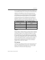
Additional Resources
For additional information, go to http://support.xilinx.com. The
following table lists some of the resources you can access from this
page. You can also directly access some of these resources using the
provided URLs.
Resource
Description/URL
Tutorial
Tutorials covering Xilinx design flows, from design entry to verification
and debugging
http://support.xilinx.com/support/techsup/tutorials/index.htm
Answers
Database
Current listing of solution records for the Xilinx software tools
Search this database using the search function at
http://support.xilinx.com/support/searchtd.htm
Application
Notes
Descriptions of device-specific design techniques and approaches
http://support.xilinx.com/apps/appsweb.htm
Mentor Graphics Interface Guide — 2.1i
i
Mentor Graphics Interface Guide
Resource
Description/URL
Data Book
Pages from The Programmable Logic Data Book, which describe devicespecific information on Xilinx device characteristics, including readback, boundary scan, configuration, length count, and debugging
http://support.xilinx.com/partinfo/databook.htm
Xcell Journals
Quarterly journals for Xilinx programmable logic users
http://support.xilinx.com/xcell/xcell.htm
Tech Tips
Latest news, design tips, and patch information on the Xilinx design
environment
http://support.xilinx.com/support/techsup/journals/index.htm
Manual Contents
This manual covers the following topics.
ii
•
Chapter 1, “Introduction,” describes the Mentor Graphics Design
Manager™ Interface, the Xilinx design flow, key features, inputs
and outputs, and the architectures with which they work.
•
Chapter 2, “Getting Started,” describes how to configure your
system for the Mentor Graphics Design Manager, and how to
invoke and exit the Mentor Graphics Design Manager.
•
Chapter 3, “Schematic Designs,” describes how to use the Mentor
Graphics Design Manager and Design Architect™ to design with
pure schematic designs. It covers, schematic design entry, functional simulation, implementation, and timing simulation.
•
Chapter 4, “HDL Designs,” describes how to use the Mentor
Graphics Interface to design with pure HDL designs. It covers,
HDL design entry, functional simulation, implementation, and
timing simulation.
•
Chapter 5, “Mixed Designs with VHDL on Top,” describes how
to use the Mentor Graphics Interface to design with mixed schematic and VHDL designs with VHDL on Top. It covers, design
entry, functional simulation, implementation, and timing simulation.
•
Chapter 6, “Mixed Designs with Schematic on Top,” describes
how to use the Mentor Graphics Interface to design with mixed
schematic and VHDL designs with schematic on top. It covers,
Xilinx Development System
design entry, functional simulation, implementation, and timing
simulation.
•
Chapter 7, “Mentor/Xilinx Flow Manager,” describes how to use
the Mentor/Xilinx Flow Manager to guide you through the
design process.
•
Chapter 8, “Advanced Techniques,” describes useful design and
simulation techniques that were not covered in the other sections
of this manual.
•
Chapter 9, “Manual Translation,” describes how to manually
process your design from the operating system command line.
Mentor Graphics Interface Guide
iii
Mentor Graphics Interface Guide
iv
Xilinx Development System
Conventions
This manual uses the following typographical and online document
conventions. An example illustrates each typographical convention.
Typographical
The following conventions are used for all documents.
•
Courier font indicates messages, prompts, and program files
that the system displays.
speed grade: -100
•
Courier bold indicates literal commands that you enter in a
syntactical statement. However, braces “{ }” in Courier bold are
not literal and square brackets “[ ]” in Courier bold are literal
only in the case of bus specifications, such as bus [7:0].
rpt_del_net=
Courier bold also indicates commands that you select from a
menu.
File → Open
•
Italic font denotes the following items.
•
Variables in a syntax statement for which you must supply
values
edif2ngd design_name
•
References to other manuals
See the Development System Reference Guide for more information.
Mentor Graphics Interface Guide — 2.1i
v
Mentor Graphics Interface Guide
•
Emphasis in text
If a wire is drawn so that it overlaps the pin of a symbol, the
two nets are not connected.
•
Square brackets “[ ]” indicate an optional entry or parameter.
However, in bus specifications, such as bus [7:0], they are
required.
edif2ngd [option_name] design_name
•
Braces “{ }” enclose a list of items from which you must choose
one or more.
lowpwr ={on|off}
•
A vertical bar “|” separates items in a list of choices.
lowpwr ={on|off}
•
A vertical ellipsis indicates repetitive material that has been
omitted.
IOB #1: Name = QOUT’
IOB #2: Name = CLKIN’
.
.
.
•
A horizontal ellipsis “. . .” indicates that an item can be repeated
one or more times.
allow block block_name loc1 loc2 ... locn;
Online Document
The following conventions are used for online documents.
vi
•
Red-underlined text indicates an interbook link, which is a crossreference to another book. Click the red-underlined text to open
the specified cross-reference.
•
Blue-underlined text indicates an intrabook link, which is a crossreference within a book. Click the blue-underlined text to open
the specified cross-reference.
Xilinx Development System
Contents
About this Manual
Additional Resources ..................................................................... i
Manual Contents ............................................................................ ii
Conventions
Typographical................................................................................. v
Online Document ........................................................................... vi
Chapter 1
Introduction
Architecture Support ...................................................................... 1-1
Platform Support ............................................................................ 1-2
Library Support............................................................................... 1-2
Features ......................................................................................... 1-2
Mentor Software Release Support............................................ 1-2
HDL Support ............................................................................. 1-2
ModelSim and QuickSim Pro............................................... 1-3
VHDL Gate-Level Simulation Support ................................. 1-3
Verilog Gate-Level Simulation Support................................ 1-3
Links to the Xilinx Synopsys Interface (XSI) ........................ 1-3
Mentor Design Manager ........................................................... 1-4
Coregen (CORE Generator) ................................................ 1-6
Editor ................................................................................... 1-6
Exemplar.............................................................................. 1-6
Flo_mgr (Mentor/Xilinx Flow Manager)................................ 1-6
Gen_Arch............................................................................. 1-6
ModelSim............................................................................. 1-6
Pld_da.................................................................................. 1-7
Pld_dsgnmgr........................................................................ 1-7
Pld_dve................................................................................ 1-8
Pld_edif2sim ........................................................................ 1-8
Pld_edif2tim ......................................................................... 1-8
Mentor Graphics Interface Guide — 2.1i
vii
Mentor Graphics Interface Guide
Pld_logiblox (LogiBLOX GUI) .............................................. 1-8
Pld_men2edif....................................................................... 1-8
Pld_xnf2sim ......................................................................... 1-8
Pld_quicksim........................................................................ 1-9
Pld_sg.................................................................................. 1-9
QuickPath ............................................................................ 1-9
QSPro (QuickSim Pro)......................................................... 1-9
Renoir .................................................................................. 1-10
LogiBLOX Modules ................................................................... 1-10
CORE Generator Modules........................................................ 1-10
EDIF.......................................................................................... 1-10
Cross-Probing ........................................................................... 1-10
Timing Simulation ..................................................................... 1-11
Schematic Generator ................................................................ 1-11
Timing Constraints .................................................................... 1-11
Design Flows.................................................................................. 1-11
Schematic Entry Design Flows ................................................. 1-12
HDL Entry ................................................................................. 1-16
Mixed Schematic and VHDL Flow with VHDL on Top .............. 1-17
Mixed Schematic and VHDL Flow with Schematic on Top ....... 1-18
Inputs ............................................................................................. 1-19
EDIF.......................................................................................... 1-19
XNF........................................................................................... 1-19
Outputs........................................................................................... 1-19
Files................................................................................................ 1-20
Tutorials ......................................................................................... 1-21
Online Help .................................................................................... 1-21
Chapter 2
Getting Started
Configuring Your System ............................................................... 2-1
Modifying Mentor Graphics Variables ....................................... 2-2
Invoking the Design Manager ........................................................ 2-4
Invoking Applications in the Design Manager ........................... 2-4
Tools Window Icons............................................................. 2-4
Navigator Window................................................................ 2-5
Exiting the Design Manager ........................................................... 2-5
Chapter 3
Schematic Designs
Design Flows.................................................................................. 3-1
Design Entry................................................................................... 3-1
Invoking Design Architect ......................................................... 3-1
viii
Xilinx Development System
Contents
Exiting Design Architect ............................................................ 3-3
Loading a Schematic ................................................................ 3-3
Creating the Design Component............................................... 3-4
Adding Components ................................................................. 3-4
Adding Xilinx library Components........................................ 3-4
Xilinx Libraries ..................................................................... 3-5
Adding Properties ..................................................................... 3-10
Properties ............................................................................ 3-11
Adding Properties ................................................................ 3-12
Adding the Net Property to Nets .......................................... 3-14
Modifying Property Values................................................... 3-14
Entering Timing Specifications ............................................ 3-16
Creating New Groups from Existing Groups........................ 3-17
Functional Simulation..................................................................... 3-17
Simulating Pure Schematic Designs......................................... 3-18
Creating the Viewpoint......................................................... 3-18
Simulating the Design.......................................................... 3-20
Simulating Schematic Designs with LogiBLOX Elements or CORE
Generator Modules ................................................................... 3-22
Simulating Schematic Designs with XNF Elements.................. 3-22
Creating the Design Component ......................................... 3-22
Converting the XNF File ...................................................... 3-22
Creating the Viewpoint......................................................... 3-25
Simulating the Design.......................................................... 3-25
Simulating Schematic Designs with EDIF Elements................. 3-25
Creating the Design Component ......................................... 3-25
Converting the EDIF File ..................................................... 3-26
Simulating the Design.......................................................... 3-27
Implementing Schematic Designs.................................................. 3-28
Converting the EDDM Design to EDIF...................................... 3-28
Implementing the Design .......................................................... 3-30
Timing Simulation for Schematic Designs...................................... 3-37
Creating the EDDM Model and the Viewpoint .......................... 3-38
Simulating the Design ............................................................... 3-40
Cross-Probing ........................................................................... 3-41
Performing a Timing Analysis ................................................... 3-43
Chapter 4
HDL Designs
The Design Flow ............................................................................ 4-1
HDL Design Entry .......................................................................... 4-2
Overview of HDL Design Entry ................................................. 4-3
HDL Design Entry Stages ......................................................... 4-4
Mentor Graphics Interface Guide
ix
Mentor Graphics Interface Guide
Stage 1: RTL Behavioral Code Development...................... 4-6
Stage 2: Synthesis............................................................... 4-7
LogiBLOX Design Entry....................................................... 4-8
CORE Generator Module Design Entry .................................... 4-9
Unified Library Instantiated Components.................................. 4-10
Functional Simulation..................................................................... 4-10
Pre-Synthesis Functional Simulation ........................................ 4-11
Synthesis .................................................................................. 4-14
Post-Synthesis Functional Simulation....................................... 4-14
Optional Post Synthesis Functional Simulation ........................ 4-17
Design Implementation .................................................................. 4-19
Timing Simulation........................................................................... 4-27
Compiling the SimPrim Libraries............................................... 4-27
Passing Timing Generics to Special Cells—ROC, OSC, OSC4, and
OSC5 ........................................................................................ 4-27
Compiling the Design................................................................ 4-29
Simulating the Design ............................................................... 4-30
Chapter 5
Mixed Designs with VHDL on Top
The Design Flow ............................................................................ 5-1
Design Entry................................................................................... 5-3
Functional Simulation..................................................................... 5-8
Compiling the Design................................................................ 5-8
Simulating the Design ............................................................... 5-9
Synthesis .................................................................................. 5-10
Optional Post-Synthesis Functional Simulation ........................ 5-11
Design Implementation .................................................................. 5-11
Timing Simulation........................................................................... 5-20
Compiling the SimPrim Libraries............................................... 5-20
Passing Timing Generics to Special Cells—ROC, OSC, OSC4, and
OSC5 ........................................................................................ 5-20
Compiling the Design................................................................ 5-22
Simulating the Design ............................................................... 5-23
Chapter 6
Mixed Designs with Schematic on Top
The Flow ........................................................................................ 6-1
Design Entry................................................................................... 6-2
VHDL Module Design Entry ...................................................... 6-3
Schematic Entry........................................................................ 6-4
Functional Simulation..................................................................... 6-5
Functional Simulation Before Synthesis ................................... 6-5
x
Xilinx Development System
Contents
Synthesis .................................................................................. 6-7
Functional Simulation After Synthesis ...................................... 6-7
Design Implementation .................................................................. 6-9
Converting the EDDM Design................................................... 6-10
Implementing the Design .......................................................... 6-11
Timing Simulation........................................................................... 6-11
Chapter 7
Mentor/Xilinx Flow Manager
Flow Manager Overview ................................................................ 7-1
Pure Schematic Design Flow ......................................................... 7-3
Pure XNF Design Flow................................................................... 7-7
Pure VHDL/Verilog Design Flow .................................................... 7-10
Mixed Sch(top)/HDL Design Flow .................................................. 7-15
Mixed Sch/HDL(top) Design Flow .................................................. 7-19
Create EDDM............................................................................ 7-19
Simulate/Implement Top HDL (Main Flow) ............................... 7-20
Simulate Synthesis Output (Optional)....................................... 7-21
Chapter 8
Advanced Techniques
Retargeting the Design to a Different Family ................................. 8-1
Merging Design Files from Other Sources ..................................... 8-4
Simulation Models.......................................................................... 8-4
Analyzing Nets from the Schematic ............................................... 8-4
Setting Global Reset and 3-State Signals...................................... 8-5
FPGA Designs .......................................................................... 8-5
CPLD Designs .......................................................................... 8-6
Using TAU...................................................................................... 8-7
Chapter 9
Manual Translation
Functional Simulation..................................................................... 9-1
Pure Schematic Designs........................................................... 9-1
Schematic Designs with XNF Elements.................................... 9-1
Schematic Designs with LogiBLOX or CORE Generator Elements 9-2
Mixed Schematic and VHDL with Schematic-on-Top Designs . 9-2
Before Synthesis.................................................................. 9-2
After Synthesis..................................................................... 9-4
HDL-at-Top Designs ................................................................. 9-5
Pure HDL Designs .................................................................... 9-5
Design Implementation .................................................................. 9-6
Schematic Designs (FPGA) ...................................................... 9-6
Schematic Designs (CPLD) ...................................................... 9-7
Mentor Graphics Interface Guide
xi
Mentor Graphics Interface Guide
HDL-at-Top Designs ................................................................. 9-8
Pure HDL Designs .................................................................... 9-9
Timing Simulation........................................................................... 9-10
Schematic Designs ................................................................... 9-10
Pure HDL Designs .................................................................... 9-11
EDIF Method........................................................................ 9-11
VHDL/Verilog Method .......................................................... 9-11
Program Summary ......................................................................... 9-12
CPLD ........................................................................................ 9-12
Dsgnmgr ................................................................................... 9-12
EDIF2NGD................................................................................ 9-13
Editor......................................................................................... 9-13
Gen_Arch.................................................................................. 9-13
MAP .......................................................................................... 9-13
NGDAnno.................................................................................. 9-13
NGDBuild .................................................................................. 9-14
NGD2EDIF................................................................................ 9-14
PAR........................................................................................... 9-14
Pld_da....................................................................................... 9-14
Pld_dve ..................................................................................... 9-14
Pld_edif2sim ............................................................................. 9-15
Pld_edif2tim .............................................................................. 9-16
Pld_men2edif ............................................................................ 9-16
Pld_quicksim............................................................................. 9-17
Pld_sg ....................................................................................... 9-18
Pld_xnf2sim .............................................................................. 9-18
ModelSim .................................................................................. 9-19
QuickPath ................................................................................. 9-20
QuickSim Pro ............................................................................ 9-20
Vcom......................................................................................... 9-20
Vlog........................................................................................... 9-20
xii
Xilinx Development System
Chapter 1
Introduction
This chapter describes the Mentor Graphics® Design Manager™
interface, a Mentor Graphics tool enhanced by the addition of Xilinx
features.
You can invoke all individual tools from the Xilinx-enhanced Design
Manager or from the shell.
This chapter contains the following sections.
•
“Architecture Support”
•
“Platform Support”
•
“Library Support”
•
“Features”
•
“Design Flows”
•
“Inputs”
•
“Outputs”
•
“Files”
•
“Tutorials”
•
“Online Help”
Architecture Support
You can use the Mentor interface with the following Xilinx architectures.
•
XC3000A/L
•
XC3100A/L
•
XC4000E/EX/L/XL/XV/XLA
Mentor Graphics Interface Guide — 2.1i
1-1
Mentor Graphics Interface Guide
•
XC5200
•
XC9500/XL
•
Spartan/XL
•
Virtex
Note: You cannot mix old XC4000EX library components with
XC4000X library components. Use Convert Design to convert
XC4000EX designs to XC4000X before instantiating new XC4000X
library components.
Platform Support
The Mentor interface is supported on Sun SPARCstations using the
Solaris operating system versions 2.5 and 2.6. It is also supported on
HP workstations using the HPUX operating system version 10.2.
Library Support
The following libraries are available in the Mentor interface.
•
Unified Libraries, which contain the symbol models for schematic entry and simulation
•
SimPrim library, which contains the symbol models for timing
(EDDM) simulation
•
VITAL VHDL SimPrim library for top-down timing simulation
•
Verilog SimPrim library for top-down Verilog timing simulation
Features
The following sections describe the major features available in this
release.
Mentor Software Release Support
This interface supports the Mentor C.2 software release.
HDL Support
This release offers a number of features that allow you to process a
design through a VHDL or Verilog netlist.
1-2
Xilinx Development System
Introduction
ModelSim and QuickSim Pro
This release supports the ModelSim™ simulator, which simulates
behavioral VHDL, Verilog, VHDL-based, and Verilog-based gatelevel designs composed of SimPrim elements. In addition, LogiBlox
elements can be simulated at the behavioral level.
It also supports QuickSim Pro™ for mixed mode simulations for
schematic-based and VHDL-based designs. QuickSim Pro can invoke
ModelSim to simulate VHDL-based elements, or quicksim to simulate Unified Libraries elements.
Note: This documentation assumes that you are using ModelSim and
QuickSim Pro. However, QuickHDL and QuickHDL Pro™ provide
the same functionality as ModelSim and QuickSim Pro. If you are
using QuickHDL instead of ModelSim or QuickHDL Pro in place of
QuickSim Pro, see the “ModelSim” section for details on how to use
QuickHDL and QuickHDL Pro in place of ModelSim and QuickSim
Pro.
VHDL Gate-Level Simulation Support
This release supports VHDL simulation, including IEEE-standard
1076.4 VHDL libraries of SimPrim models. Xilinx implementation
tools output timing simulation VHDL netlists by using structural
VHDL models of SimPrim VHDL models and an SDF file.
Verilog Gate-Level Simulation Support
This release supports Verilog simulation, including Verilog libraries
for use with SimPrim models. Xilinx implementation tools output
timing Verilog netlists by using structural Verilog models with
SimPrim Verilog models and an SDF file.
Links to the Xilinx Synopsys Interface (XSI)
The Mentor interface can accept Synopsys synthesized netlists in the
form of SEDIF or SXNF files. It can also accept XNF and EDIF files
from other synthesizers that are compatible with the Xilinx implementation software. These files can be directly submitted to the Xilinx
Design Manager for placement and routing of the design.
You can also simulate these EDIF or SXNF files by submitting them to
the pld_edif2sim or pld_xnf2sim utility, which creates EDDM components for use with pld_quicksim.
Mentor Graphics Interface Guide
1-3
Mentor Graphics Interface Guide
In addition, after place and route, you can output VHDL and Verilog
netlists, which can be submitted to ModelSim for simulation with
SDF files providing the back-annotation information.
Mentor Design Manager
The Mentor Graphics Design Manager is an easy-to-use interface that
represents applications and design files as icons. You can now
perform many tasks in the Design Manager window that were previously done at the operating system level. The Design Manager runs
in a window on your workstation display and makes it easy for you
to invoke applications and to manage designs, files, and directories.
The Design Manager lets you do these tasks by using graphical pointand-click actions. You can run applications by selecting an application icon, or a design object icon and a menu item.
Note: A design object consists of the files and directories that make
up your design.
The Xilinx script, pld_dmgr, configures the Design Manager for the
creation, implementation, and simulation of Xilinx designs. This
manual describes only the Xilinx-configured Design Manager; refer
to Mentor Graphics documentation for a more comprehensive
description of the Mentor Design Manager.
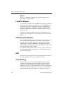
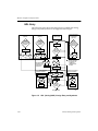
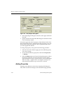
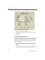
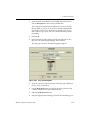
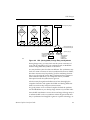
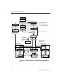
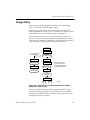
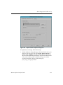
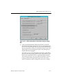
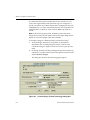
The Design Manager includes a Tools window, a Navigator window,
and a Design Manager palette, as shown in the following figure.
1-4
Xilinx Development System
Introduction
Figure 1-1 Mentor Design Manager Window
The Tools window contains icons representing all the Mentor
Graphics and Xilinx applications that you need to execute the steps in
the design flow. The Navigator window contains design object icons,
including original schematics as well as files created during translation and simulation. This window makes it easy to access files in
different directories. The Design Manager palette provides easy
access to the most commonly used Design Manager menu items.
The remainder of this section briefly describes the icons in the Tools
window and the Mentor programs they represent. The tools with
names that begin with PLD are configured through scripts for
working with Xilinx designs.
Mentor Graphics Interface Guide
1-5
Mentor Graphics Interface Guide
Coregen (CORE Generator)
This is a stand-alone Xilinx tool for generating VHDL and Verilog
models of CORE modules. Schematic models can be created by
invoking CORE Generator from within pld_da under the Xilinx
Libraries Palette menu.
Editor
The Editor icon represents the Mentor Graphics Notepad editor.
Notepad is a full-featured, window-based text editor. For more information on Notepad, refer to the Mentor Graphics Notepad User’s and
Reference Manual.
Exemplar
The Exemplar™ icon opens the Leonardo™ Spectrum synthesis tool.
Flo_mgr (Mentor/Xilinx Flow Manager)
The Mentor/Xilinx Flow Manager is a dialog box that provides a
visual guide of the steps you need to perform for five common design
flows. Each step contains buttons to launch the appropriate tool and
to display a visual record of your progress in the flow. It does not
automatically perform the steps for you. It lists the steps in the correct
order that you need to perform. For each step there is a button that
launches the appropriate tool. When you are finished with the tool,
you click on the Finished button for that step and the description for
that step changes to indicate that it is finished.
Gen_Arch
Gen_Arch creates a VHDL architecture from a Mentor schematic
(EDDM) component for use in mixed schematic and HDL simulations within QuickSim Pro.
ModelSim
ModelSim™ (vsim) is Mentor’s simulator for behavioral VHDL,
Verilog, or VHDL-based and Verilog-based gate-level designs
composed of SimPrim elements.
QuickHDL previously provided this same functionality as ModelSim.
The design flows in this user guide are based on ModelSim. If you
1-6
Xilinx Development System
Introduction
have not upgraded to ModelSim and are still using QuickHDL, you
can substitute QuickHDL into your design flows as described below.
ModelSim and QuickHDL have the same functionality, but the
commands you use to control these tools are different. The Mentor
Design Manager contains icons for QHDL as well as ModelSim so
you can access either tool depending on what you have installed.
The following table provides a mapping between ModelSim and
QuickHDL commands. In the procedures in this manual that use
ModelSim commands, you can substitute QuickHDL by substituting
the corresponding QuickHDL commands in those procedures.
ModelSim Commands
QuickHDL Commands
vsim
qhsim
vlib
qhlib
vmap
qhmap
vcom
qvhcom
vlog
qvlcom
Pld_da
Pld_da is Mentor’s Design Architect®, a schematic editor configured
for Xilinx designs. The Xilinx-configured Design Architect is identical
to the Mentor Graphics version except for the addition of a Xilinx
library of primitives, macros, and utilities such as Convert Design.
For more information on creating Xilinx designs with Design Architect, refer to the “Design Entry” section of the “Schematic Designs”
chapter in this manual and the Mentor Graphics Schematic Design Tutorial on the Xilinx Web site at http://support.xilinx.com/support/
techsup/tutorials/index.htm. For a more detailed description of
Design Architect commands and processes, refer to the Mentor
Graphics Design Architect User’s Manual.
Pld_dsgnmgr
The Mentor Design Manager interface contains a Pld_dsgnmgr icon
for the Xilinx Design Manager. Pld_dsgnmgr is the Xilinx Design
Manager, which implements the design. You can access any individual Xilinx tool from the Xilinx Design Manager.
Mentor Graphics Interface Guide
1-7
Mentor Graphics Interface Guide
Pld_dve
Pld_dve is the Mentor Graphics Design Viewpoint Editor (DVE)
configured for Xilinx designs. When you invoke this application from
within the Mentor Design Manager, a dialog box appears and you are
asked to create either a simulation or custom viewpoint. Refer to the
“Functional Simulation” section of the “Schematic Designs” chapter
and the “Timing Simulation for Schematic Designs” section of the
“Schematic Designs” chapter in this manual for more information on
pld_dve. For detailed information on DVE, refer to the Mentor
Graphics Design Viewpoint Editor User’s and Reference Manual.
Pld_edif2sim
Pld_edif2sim is a utility that converts a Mentor, Synopsys, or other
Xilinx compatible EDIF file into a Mentor EDDM single-object simulation model, VHDL netlist, or Verilog netlist. Pld_edif2sim is for
functional simulation only.
Pld_edif2tim
Pld_edif2tim is the Mentor EDIF netlist reader, which converts a
placed and routed EDIF netlist to a Mentor single-object EDDM file
that can be submitted to pld_quicksim for timing simulation.
Pld_logiblox (LogiBLOX GUI)
This is a stand-alone Xilinx tool for generating VHDL and Verilog
models of LogiBlox components. Schematic models can be created by
invoking LogiBLOX from within pld_da under the Xilinx Libraries
Palette menu.
Pld_men2edif
Pld_men2edif converts a Mentor schematic to a hierarchical EDIF
netlist that is ready for implementation.
Pld_xnf2sim
Pld_xnf2sim is a utility that converts an unrouted XNF file to a
Mentor EDDM single-object simulation model. This conversion can
only be done on chip-level XNF files with EXT records, not on lower
level modules embedded in a schematic. VHDL or Verilog simulation
1-8
Xilinx Development System
Introduction
models can also be generated. Pld_xnf2sim is for functional simulation only.
Pld_quicksim
Pld_quicksim is an interactive logic simulator that performs functional or timing simulation on your designs. For more information on
pld_quicksim, refer to the “Functional Simulation” section of the
“Schematic Designs” chapter, the “Timing Simulation for Schematic
Designs” section of the “Schematic Designs” chapter, and the Mentor
Graphics Schematic Design Tutorial on the Xilinx Web site at http://
support.xilinx.com/support/techsup/tutorials/index.htm. For a
detailed description of pld_quicksim, refer to the Mentor Graphics
QuickSim II User’s Manual.
Pld_sg
Pld_sg is the Mentor schematic generator (SG), which creates a schematic from an EDDM single object netlist. You can use this tool to
generate a schematic for the timing simulation netlist.
QuickPath
QuickPath™ performs static and slack timing analysis on designs.
For more information on QuickPath, refer to the “Performing a
Timing Analysis” section of the “Schematic Designs” chapter. For a
detailed description of QuickPath, refer to the Mentor Graphics
QuickPath User’s and Reference Manual.
QSPro (QuickSim Pro)
QuickSim Pro™ (qspro) is Mentor’s simulator for mixed schematicbased, VHDL-based, and Verilog-based designs. It can invoke
ModelSim to simulate HDL-based elements, or pld_quicksim to
simulate Unified Schematic Library elements.
Note: This documentation assumes that you are using ModelSim and
QuickSim Pro. However, QuickHDL and QuickHDL Pro™ provide
the same functionality as ModelSim and QuickSim Pro. If you are
using QuickHDL instead of ModelSim or QuickHDL Pro in place of
QuickSim Pro, see the “ModelSim” section for details on how to use
QuickHDL and QuickHDL Pro in place of ModelSim and QuickSim
Pro.
Mentor Graphics Interface Guide
1-9
Mentor Graphics Interface Guide
Renoir
Renoir™ is the Mentor Graphics HDL graphical design tool for
generating Verilog and VHDL.
LogiBLOX Modules
You can enter a schematic using LogiBLOX symbols along with other
Unified Libraries elements. For schematics, invoke LogiBLOX from
within pld_da by using the Xilinx Libraries menu (Libraries →
Xilinx Libraries → Logiblox). In addition, EDDM simulation
models are automatically created for LogiBLOX symbols during
symbol creation.
For VHDL or Verilog LogiBlox models, invoke LogiBlox from the
pld_dmgr’s tool window, or from the popup session window within
pld_da.
CORE Generator Modules
You can enter a schematic using CORE Generator symbols along with
other Unified Libraries elements. For schematics, invoke CORE
Generator from within pld_da by using the Xilinx Libraries menu
(Libraries → Xilinx Libraries → Coregen). In addition,
EDDM simulation models are automatically created for CORE Generator symbols during symbol creation.
For VHDL or Verilog CORE Generator models, invoke CORE Generator from the pld_dmgr’s tool window, or from the popup session
window within pld_da.
EDIF
This release supports EDIF 2 0 0 for design implementation. Refer to
the Xilinx EDIF specification for supported constructs.
Cross-Probing
Cross-probing is a way of cross-referencing between the original
schematic and the timing simulation model after placement and
routing. Once a Mentor design is translated, expanded, mapped,
placed, and routed, you can extract the back-annotation information
and create a hierarchical EDIF netlist. After you convert this EDIF to
an EDDM model using pld_edif2tim, you submit it to pld_dve to
1-10
Xilinx Development System
Introduction
create a viewpoint and then to pld_quicksim for timing simulation.
The resulting data base preserves the design hierarchy, and although
it is created in terms of the SimPrim library, most of the original net
names are still available. You enable cross-probing by invoking
QuickSim with the -cp option. This option invokes pld_dve as well as
pld_quicksim. You then open the original design viewpoint in
pld_dve and view the desired design sheet. If you display the original schematic in pld_dve, you can select nets on the original schematic and view them in the QuickSim trace window.
See the “Cross-Probing” section of the “Schematic Designs” chapter
for more details on cross-probing.
Timing Simulation
This release supports back-annotated timing simulation after placement and routing. Pld_edif2tim translates the routed EDIF file to an
EDDM single-object netlist.
Schematic Generator
The schematic generator is a utility that you can optionally use to
generate a hierarchical schematic from a back-annotated EDDM
model. This is not a required step since you can instead use crossprobing with the back-annotated EDDM model and the original schematic for simulation without generating a back-annotated schematic.
You can invoke the schematic generator from within the design
manager or from a shell by typing pld_sg. You must have a Mentor
schematic generator license in order to use this tool.
Timing Constraints
You can add timing constraints to the schematic as properties. You
can also place them in a UCF (user constraints file) that NGDBuild
can process. If a conflict arises between the timing information in the
EDIF file and in the constraints file, the information in the constraints
file prevails.
Design Flows
You use different PLD design flows for performing design entry,
implementation and simulation depending on whether you use schematic design entry or HDL design entry.
Mentor Graphics Interface Guide
1-11
Mentor Graphics Interface Guide
In either case, the easiest and most automatic way is to use the application icons in the Design Manager window. You can also run the
various programs in the design flow manually from the UNIX shell.
The shell commands are described in the “Manual Translation”
chapter.
The Mentor interface supports the following design flows.
•
Schematic entry with the Unified Libraries components, LogiBLOX symbols, CORE Generator symbols or a combination of
these symbols.
•
Schematic entry with Unified Library components with some
models expressed in Xilinx compliant EDIF or XNF
•
Top-down HDL (Verilog/VHDL) design entry and synthesis
•
Mixed schematic and VHDL design with VHDL on top
•
Mixed schematic and VHDL design with schematic on top
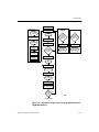
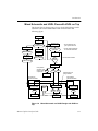
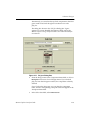
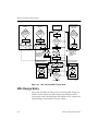
Schematic Entry Design Flows
The schematic entry design flows are illustrated in the following
three figures.
1-12
Xilinx Development System
Introduction
pld_dmgr
EDIF (optional)
EDIF
lower-level
module
LogiBLOX
(optional)
pld_da
EDDM
Design
contains
LogiBLOX
elements
pld_edif2sim
with EDIF for module
CORE Generator
(optional)
Design
contains
CORE Generator
modules
pld_dve
EDDM
single object
Create Mentor
symbol
with pld_da
Add property
File=EDIF
to symbol
pld_quicksim
Design
functionality
correct?
LogiBLOX GUI
CORE Generator
EDDM
single object
and symbol
EDDM
single object
and symbol
No
Yes
Instantiate into
top-level
schematic
pld_men2edif
EDIF
pld_dsgnmgr
EDIF with timing
pld_edif2tim
EDDM
single object
pld_dve
pld_quicksim
(with cross-probing)
Yes
Design
timing
correct?
No
X8883
Yes
Design complete
Figure 1-2 Schematic Design Entry Including EDIF-Based and
LogiBLOX Modules
Mentor Graphics Interface Guide
1-13
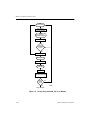
Mentor Graphics Interface Guide
XNF
top-level module
pld_xnf2sim
with top-level XNF
EDDM
single object and
simulation viewpoint
pld_quicksim
Design
functionality
correct?
No
Yes
pld_dsgnmgr
EDIF with timing
pld_edif2tim
EDDM
single object
pld_dve
pld_quicksim
(without cross-probing)
Yes
Design
timing
correct?
Yes
No
X8884
Design complete
Figure 1-3 Design Entry with XNF Top-Level Module
1-14
Xilinx Development System
Introduction
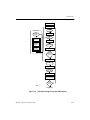
pld_dmgr
pld_da
EDDM
XNF (optional)
XNF
lower-level
module
pld_men2edif
EDIF
Create Mentor
symbol
with pld_da
Add property
File=
XNF_pathname
to symbol
Instantiate into
top-level
schematic
pld_edif2sim
on top
EDDM
single object
pld_quicksim
Design
functionality
correct?
No
Yes
pld_dsgnmgr
EDIF with timing
pld_edif2tim
EDDM
single object
pld_dve
pld_quicksim
(with cross-probing)
Yes
Design
timing
correct?
X8885
No
Yes
Design complete
Figure 1-4 Schematic Design Entry with XNF Module
Mentor Graphics Interface Guide
1-15
Mentor Graphics Interface Guide
HDL Entry
The following figure shows the design flow for VHDL and Verilog
design entry and synthesis for all supported technologies.
CORE Generator
(optional)
LogiBLOX
(optional)
HDL Entry Tool
(DA, Renoir, Text)
Design
contains
instantiations of
CORE Generator
modules
Design
contains
instantiations
of LogiBLOX
elements
RTL
HDL
CORE Generator
LogiBLOX GUI
VHDL
EDIF
Verilog
VHDL
NGC
Verilog
Instantiated Unified
Library (Unisim)
Componments
(optional)
Design
contains
instantiations
of Unified Library
components
ModelSim
Design
functionality
correct?
No
Yes
VHDL
Verilog
VHDL
Synthesis*
Verilog VHDL
Post-synthesis
simulation using
Unified Library
ModelSim
components
EDIF
* Do not synthesize
architectures for
LogiBLOX or
CORE Generator
modules
XNF
pld_dsgnmgr
Optional post-synthesis
gate-level simulation
pld_edif2sim
on top-level EDIF
VHDL Verilog
ModelSim
Optional post-synthesis
gate-level simulation
VHDL
SimPrim
VHDL/
Verilog
SDF
Verilog
pld_xnf2sim
on top-level XNF
ModelSim
VHDL
Design
timing
correct?
No
Verilog
ModelSim
Yes
Design complete
X8887
Figure 1-5 HDL (Verilog/VHDL) Design Entry and Synthesis
1-16
Xilinx Development System
Introduction
Mixed Schematic and VHDL Flow with VHDL on Top
The design flow for design entry of a top-level VHDL design with a
schematic sub-module embedded within is illustrated in the
following figure.
pld_dmgr
pld_da
HDL Entry Tool
(DA, Renoir, Text)
EDDM for
schematic module
pld_men2edif*
pld_dve
RTL VHDL to be
synthesized
Gen_Arch
QuickSim Pro
*Use bus delimiters that
your synthesis tool uses
**Do not compile architecture
for schematic instantiation
EDIF for module
pld_edif2sim
NGO only
VHDL for module
No
NGO for module
RTL functional simulation
Design
correct?
Yes
Synthesis**
Post-synthesis
simulation using
Unified Library
VHDL
components
EDIF
XNF
Implementation and
timing simulation
QuickSim Pro
Post-synthesis
gate level simulation
pld_edif2sim
on top level EDIF
VHDL
ModelSim
Post-synthesis
gate level simulation
SimPrim
VHDL
pld_dsgnmgr
VHDL
SDF
ModelSim
pld_xnf2sim
on top level XNF
VHDL
ModelSim
X8850
Figure 1-6 Mixed Schematic and VHDL Design with VHDL on
Top
Mentor Graphics Interface Guide
1-17
Mentor Graphics Interface Guide
Mixed Schematic and VHDL Flow with Schematic on
Top
The design flow for design entry using a mixture of schematics,
VHDL, and Verilog is illustrated in the following figure.
pld_dmgr
HDL Entry tool
(DA, Renoir, Text)
RTL VHDL
for module
vcom
Compiled VHDL
for module
PLD_DA
Generate Symbol
in pld_da for
HDL module
Design
correct?
No
Yes
pld_men2edif*
* Use bus delimiters
that your synthesis
tool uses
Synthesis
or
Top-level
EDIF
EDIF
for module
XNF
for module
Import VHDL
Instantiate on top
level schematic
pld_dsgnmgr
Put file=xnf or
file=edif property on
symbol of synthesized
module
EDDM for design
with instantiated
VHDL module
Optional
post-synthesis
gate-level
simulation
Routed EDIF
in SimPrims
pld_edif2sim
on top-level EDIF
pld_edif2tim
Unrouted EDDM
in Simprims
Routed EDDM
in Simprims
pld_quicksim
pld_dve
pld_dve
QuickSim Pro
pld_quicksim
X8851
Figure 1-7 Mixed Schematic and VHDL Design with Schematic
on Top
1-18
Xilinx Development System
Introduction
Inputs
The Mentor interface accepts netlists in EDIF or XNF format.
EDIF
You can submit an EDIF Level 2 0 0 netlist based on a design using
Unified Libraries components. The following restrictions apply.
•
Only the netlist and schematic types of EDIF are supported.
•
Only one design per EDIF file is allowed.
•
An EDIF file can contain one design component or multiple
components. The EDIF2NGD utility converts each design component to an NGO file. NGDBUILD uses a top-level NGO file,
which refers to the other NGO files, to create the NGD file.
XNF
The Mentor interface can accept one of the following XNF netlists.
•
An XNF netlist created by third-party netlist writers that meet the
specifications of XNF version 6.1
•
An XFF netlist created by XNFMerge version 6.1
•
An XTF netlist created by XNFPrep version 6.1
An XNF netlist can represent all or part of a design. To be included in
the netlist of a schematic design, a component must be tagged with
the FILE property indicating the path name of the XNF file.
If a lower module is expressed in XNF, the top level must be run
through EDIF2SIM in order to create a simulation netlist. The lowerlevel XNF file can not be run through XNF2SIM by itself since its lack
of EXT records prevents XNF2SIM from knowing which signals
should become module pins.
Outputs
The Mentor interface generates a back-annotated simulation netlist
file based on the following.
•
QuickPart-based SimPrim models and a flat/hierarchical EDIF
netlist.
Mentor Graphics Interface Guide
1-19
Mentor Graphics Interface Guide
•
VHDL-based SimPrim models, a structural VHDL netlist, and a
SDF delay file.
•
Verilog-based SimPrim models, a structural Verilog netlist, and a
SDF delay file.
Files
The following Xilinx specific files are involved in processing a design
through the Mentor interface.
1-20
•
The EDN file is a post-route EDIF netlist file that expresses timing
in SimPrim library elements instead of Unified Libraries
elements.
•
The NCD file contains a representation of the physical design.
•
The NGA file contains physical timing delay information.
•
The NGD file contains a logical design hierarchy expressed in the
Xilinx implementation primitives.
•
The NGM file contains a representation of the logical design. It
also contains optimization information.
•
The NGO file contains netlist information in a proprietary data
base format; it is a binary file.
•
The SDF file contains timing delay information.
•
The V file contains the structural design based on Verilog-based
SimPrim models.
•
The VHD file contains the structural design based on VHDLbased SimPrim models.
•
The XNF file is the Xilinx netlist format used prior to the use of
EDIF in the current release. In the current Mentor Interface flow,
XNF is only used as an import format option.
•
The PCF file is the physical constraints file.
•
The UCF file is the User Constraint File for specifying the user’s
timing and placement constraints for place and route.
Xilinx Development System
Introduction
Tutorials
It is highly recommended that you perform the Mentor Interface tutorials provided on the Xilinx Web site to become familiar with the
basic concepts of PLD design, verification, and implementation. The
tutorials are located at http://support.xilinx.com/support/techsup/
tutorials/index.htm.
Online Help
The Mentor interface contains online help which is available from
each application’s dialog box. Help contains information about the
Mentor features offered in the interface but does not contain information about the Xilinx features. The Mentor software is supplied with a
set of online manuals in PDF format. This online manual is the documentation for the Xilinx features.
Mentor Graphics Interface Guide
1-21
Mentor Graphics Interface Guide
1-22
Xilinx Development System
Chapter 2
Getting Started
This chapter describes how to configure your system for the Mentor
Graphics Design Manager, and how to invoke and exit the Mentor
Graphics Design Manager. This chapter contains the following
sections.
•
“Configuring Your System”
•
“Invoking the Design Manager”
•
“Exiting the Design Manager”
Configuring Your System
Install the appropriate software and verify that your system is properly configured as described in the release notes that came with your
software package. When you have finished the installation, verify
that your .cshrc or setup file contains lines similar to the following.
setenv XILINX location_of_Xilinx_software
setenv LCA $XILINX/mentor/data
setenv SIMPRIMS $LCA/simprims
set path=($XILINX/bin/sol \
$XILINX/mentor/bin/sol $MGC_HOME/bin
$path )
Note: Path names of directories will vary. (For example, $XILINX/
bin/sol would be $XILINX/bin/hp if you are running the Xilinx software on an HP workstation.) For more information on paths and
environment variables, refer to the release notes that came with your
software package.
XILINX is the directory where all Xilinx software is located.
LCA is the directory which includes Mentor-Interface files such as
Xilinx libraries, translators, and scripts.
Mentor Graphics Interface Guide — 2.1i
2-1
Mentor Graphics Interface Guide
SIMPRIMS is the directory where the Mentor SimPrim models are
located.
Modifying Mentor Graphics Variables
Make sure that the following Mentor Graphics specific variables are
set correctly.
•
EXEMPLAR
This variable should point to the location where the Exemplar
software is installed. For example.
setenv EXEMPLAR /products/leonardo.ver4_2
•
LCA
In addition to instantiating it in the file pointed to by
MGC_LOCATION_MAP, the LCA environment variable should
point to the directory where the Xilinx/Mentor Graphics software is installed, typically $XILINX/mentor/data.
•
LD_LIBRARY_PATH
This variable is used by Mentor Graphics and Xilinx programs.
On a SPARCstation with OpenWindows installed in /usr, this
variable is set as follows.
setenv LD_LIBRARY_PATH $MGC_HOME/shared/
lib:$MGC_HOME/lib:$XILINX/bin/sol:/usr/openwin/lib
On HP workstations, the variable is SHLIB_PATH. Leave out /
usr/openwin/lib.
•
MGC_GENLIB
This should point to the Mentor Graphics gen_lib library,
normally $MGC_HOME/gen_lib.
•
MGC_HOME
This should point to the Mentor Graphics software tree.
•
MGC_LOCATION_MAP
This variable should point to a valid location map file.
Each component in a design contains a reference indicating
where it resides on the disk or network. All components in
designs created in the Mentor Graphics C.x environment refer-
2-2
Xilinx Development System
Getting Started
ence the variable $LCA, while back-annotated timing models
reference the variable $SIMPRIMS. It is also important that the
$LCA and $SIMPRIMS variables be instantiated, but not defined,
in the file pointed to by $MGC_LOCATION_MAP. With all these
elements, the location-map file should, at a minimum, look like:
MGC_LOCATION_MAP_1
(empty line)
$MGC_GENLIB
(empty line)
$LCA
(empty line)
$SIMPRIMS
(empty line)
The MGC_LOCATION_MAP_1 line indicates that this is a
version 1 location-map file. (You can also use the version
MGC_LOCATION_MAP_2, which adds features such as outside
file inclusion.) The three soft names with blank lines indicate that
the Mentor Graphics software should pull the associated values
from the parent environment.
Refer to the Mentor Graphics documentation for more information on location maps.
•
MGC_WD (Optional)
This variable should point to the working directory. You can have
this variable always point to your current directory by setting it
to “.”
Xilinx tools ignore the MGC_WD variable.
•
MGLS_LICENSE_FILE
This variable must point to a valid FlexLM license file that lists
the Mentor Graphics license daemon and licensed software
features, as supplied by Mentor Graphics. A sample license file
may begin as follows.
SERVER tequiero 9542df17 1700
DAEMON mgcld /tools/mentor/lib/mgcld
/usr/local/data/mentor.opt
FEATURE falconfw_s 8.0 31-dec-1997 10 ...
Mentor Graphics Interface Guide
2-3
Mentor Graphics Interface Guide
•
MODELTECH
This variable should point to the directory where the Modeltech
software is installed. For example.
setenv MODELTECH /products/modeltech_ver5
•
MTI_HOME
This variable should point to the directory where the Modeltech
software is installed. For example.
setenv MTI_HOME /products/modeltech_ver5
•
RENOIRHOME
This variable should point to the directory where the Renoir software is installed. For example.
setenv RENOIRHOME /products/renoir
•
SIMPRIMS
This points to the directory where Xilinx simulation models are
located. This should be set to $LCA/simprims.
Refer to the release notes for additional information on paths and
environment variables.
Invoking the Design Manager
To invoke the Design Manager from the operating system, type
pld_dmgr.
The Design Manager window appears, as shown in the “Mentor
Design Manager Window” figure of the “Introduction” chapter.
Invoking Applications in the Design Manager
You can use either an icon or the Navigator to invoke an application
from the Design Manager.
Tools Window Icons
To use an icon to open an application, double-click the left mouse
button on the icon in the Tools window.
A dialog box appears that allows you to set options, or the application is executed.
2-4
Xilinx Development System
Getting Started
Navigator Window
If you want to load a specific design, you can also use another
method of invoking an application.
1.
Select the design object in the Navigator window with the left
mouse button, and press the right mouse button.
2.
Select Open from the Navigator menu.
3.
Select the appropriate application from the popup menu.
Only the applications that can be executed on the selected object will
be displayed in the popup menu.
A dialog box appears that allows you to set options, or the application is executed.
Exiting the Design Manager
To exit the Design Manager, move the cursor to the title bar of the
Design Manger window, press the right mouse button, and select
Quit from the popup menu
Mentor Graphics Interface Guide
2-5
Mentor Graphics Interface Guide
2-6
Xilinx Development System
Chapter 3
Schematic Designs
This chapter describes how to use the Mentor Graphics Design
Manager and Design Architect to design with pure schematic
designs. It contains the following sections.
•
“Design Flows”
•
“Design Entry”
•
“Functional Simulation”
•
“Implementing Schematic Designs”
•
“Timing Simulation for Schematic Designs”
Design Flows
Three pure schematic design flows are shown in the “Schematic Entry
Design Flows” section of the “Introduction” chapter. This chapter
describes how to work with designs using the pure schematic design
flows.
Design Entry
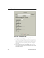
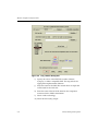
Invoking Design Architect
You can use either the pld_da icon or the Navigator to invoke Design
Architect from the Design Manager.
To invoke Design Architect with the pld_da icon in the Tools
Window, double-click the left mouse button on the pld_da icon. A
Design Architect window similar to that shown in the “Design Architect Window” figure appears but without displaying a schematic. You
can use the Open Sheet icon in the Session Palette to open a schematic
sheet.
Mentor Graphics Interface Guide — 2.1i
3-1
Mentor Graphics Interface Guide
If you want to load a specific design, you can invoke Design Architect
from the Navigator as follows.
1.
Select the design in the Navigator window and press the right
mouse button.
2.
Select Open → pld_da from the Navigator pop-up menu.
A Design Architect window similar to that shown in the
following figure appears.
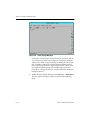
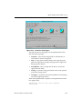
Figure 3-1 Design Architect Window
3-2
Xilinx Development System
Schematic Designs
Exiting Design Architect
To exit Design Architect, move the cursor to the title bar of the Design
Architect window, press the right mouse button, and select Quit
from the popup menu.
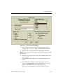
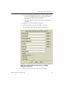
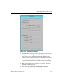
Loading a Schematic
If a design is not loaded into the schematic window, the Session
Palette (session_palette) appears on the right-hand side of the Design
Architect window. If one design is presently loaded and you want to
also load another design, click on the Session icon in the
schemataic_add_route Session Palette.
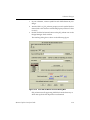
To load an existing schematic into the Design Architect window,
follow these steps.
1.
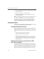
Click on the Open Sheet icon in the Session Palette.
The Open Sheet dialog box appears, as shown in the following
figure.
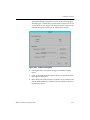
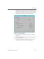
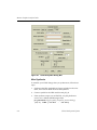
Figure 3-2 Open Sheet Dialog Box
2.
To find an existing design, type the path and name of the component or schematic in the Component Name field, or click on
Navigator to find it.
Note: If the component has not yet been created, open pld_da in the
Tool Window. Then open a sheet from the Session Palette. In the
Open Sheet dialog box, assign the component a name and click OK.
Mentor Graphics Interface Guide
3-3
Mentor Graphics Interface Guide
3.
In the Sheet field, type the name of the schematic sheet that you
want to display.
4.
In the Open As field, select Editable.
5.
Click on OK.
The schematic sheet now appears in the Design Architect
window. The schematic number, name of the design, and sheet
number appear in the title bar. The Session Palette changes to the
Schematic Palette (schematic_add_route).
Creating the Design Component
When you save your schematic in Design Architect, the following
items are created.
•
A design.mgc_component.attr file
•
A design component directory
The design component directory may contain schematic files, symbol
files, and viewpoint files. The design directory and the
design.mgc_component.attr file together are known as a Mentor
component object.
Adding Components
Adding Xilinx library Components
1.
To add a component from the Xilinx libraries, select
XILINX Libraries from the Libraries pull-down menu.
2.
In the Schematic Palette, click on the desired technology library.
Note: You cannot mix old XC4000EX library components with
XC4000X library components. Use Convert Design to convert
XC4000EX designs to XC4000X before instantiating new XC4000X
library components.
3-4
3.
Click on BY TYPE to select a category of element, or ALL PARTS
to select a specific element.
4.
Click on the desired element, move the cursor to the desired location on the schematic, and click on the left mouse button to place
it.
Xilinx Development System
Schematic Designs
Xilinx Libraries
In Design Architect, the Xilinx Libraries menu contains the Unified
Libraries. The Unified Libraries are a collection of libraries that
conform to standards set for the appearance, function, and naming
conventions of the library elements. This standardization allows you
to easily convert from one Xilinx architecture to another. You should
use the primitives and the macros in the Unified Libraries to create
new designs. Refer to the Xilinx Libraries Guide for detailed information on the Xilinx Libraries.
Primitives and Macros
The Xilinx Libraries contain the following types of components.
•
Primitives—These are pads and basic logic elements, such as
gates, latches, flip-flops, buffers, and oscillators.
•
Soft macros—These are schematics that contain primitives and
other soft macros. Soft macros have pre-defined functionality and
often have fixed mapping, placement, and routing to provide the
most efficient use of resources and the fastest speed.
LogiBLOX
LogiBLOX allows you to synthesize common data functions such as
addition, that are optimized for a particular family. Refer to the LogiBLOX Guide for information on LogiBLOX components.
CORE Generator System
The CORE Generator system allows you to use complex functions
such as math functions, memories, or DSP functions that are optimized for a particular family. Refer to the CORE Generator Guide for
information on CORE Generator modules.
You might like to create various functions using Xilinx Cores and put
them on a schematic sheet in Mentor Design Architect, and simulate
them using Mentor's QuickSim.
To place Core Generator modules into your design, follow these
steps.
1.
Invoke pld_da and open a schematic sheet for your design.
2.
In the Xilinx library menu in the schematic sheet, click on the
Coregen... Palette menu item.
Mentor Graphics Interface Guide
3-5
Mentor Graphics Interface Guide
The Create/Instantiate COREGEN Symbol dialog box opens as
shown in the following figure.
Figure 3-3 Create/Instantiate COREGEN Symbol
Note: When you invoke Coregen from within Schematic Editor, a
revolving cursor indicates that Design Architect is waiting on
Coregen GUI and for you to create a core. At times, Coregen GUI may
be hidden behind the Design Architect window. If Coregen GUI does
not come up, press control-s to stop the waiting process. When you
press control-s, the revolving cursor stops moving but it does not
return to the normal arrow shape. This does not mean that Design
Architect is not functional; you can continue working in Schematic
Editor. To restore the cursor to the normal arrow, press control-k at
any time. If you wish to continue waiting for interaction with
Coregen GUI, press control-q to resume the waiting process.
The Create/Instantiate COREGEN Symbol dialog box contains
the following fields.
3-6
Xilinx Development System
Schematic Designs
3.
•
Project directory—This is the directory in which you would
like the symbol component to reside in, we will refer to this
directory as the symbol project directory.
•
Replace existing symbol—This choice button determines if
the new symbol can over-write the same name symbol in the
symbol project directory.
•
Simulation Model—This switch can not be changed. It indicates that the cores are created from EDIF files and read into
Mentor to create EDDM SINGLE OBJECT simulation model.
•
Instantiate symbol—This choice button determines if the
created core symbol is to be placed on the sheet.
•
Target Architecture—This is a list gadget from which the
desired Xilinx family is selected.
Fill out this form and click OK.
The CORE Generator system is invoked and Design Architect is
disabled.
4.
In the CORE Generator, select and generate the desired core.
5.
Once the CORE Generator edif output is created control will be
back in the Design Architect, a symbol gets created and user is
able to place the symbol on the schematic sheet.
6.
Upon placement of the symbol an automatic popup message
inquires if you would like to create another core. If you select
YES, the control will be transferred back to CORE Generator and
the same process repeats. If you select NO, the CORE Generator
GUI automatically closes. This dialog box often appears on the
top left corner of the schematic window.
7.
After the CORE Generator closes, if you need to create another
core, go back to step 2 above.
Using the Xilinx Libraries
The following procedure describes selecting a component from the
Unified Libraries and placing it in your schematic. Do not mix
components from different technologies (families).
From within Design Architect, select and place library components as
follows.
Mentor Graphics Interface Guide
3-7
Mentor Graphics Interface Guide
1.
Select XILINX Libraries from the Libraries pull-down menu.
The schematic palette is replaced by the Xilinx libraries menu
palette.
2.
Select the correct library for your design. A menu appears and
you can select BY TYPE or ALL PARTS. If you select By Type, a
list of the components organized into categories such as buffer,
counter, or flip_flop appears. If you select All Parts, all the
components are displayed in alphabetical order. Use the Page Up
and Page Down keys to move up and down the list of components.
3.
Select a component from the library list.
4.
Move the cursor into the schematic window. An outline of the
selected component appears.
5.
Move the outline to the appropriate location and click the left
mouse button to place the component.
Bus Rippers
Bus rippers are Mentor Graphics-supplied special components that
connect nets to specific signals on a bus. You can obtain bus rippers
by selecting the rip component in the Logic submenu in the Unified
Libraries. These components are the same as rip components in the
MGC Digital Libraries gen_lib.
A bus ripper consists of two pins. The narrow end is the wire end and
the wide end is the bundle end. The wire end always connects to a net
or smaller bus, and the bundle end connects to a bus. The bus ripper
can tap all or a set of signals into a new bus. Refer to the following
figure for an example of a bus ripper.
3-8
Xilinx Development System
Schematic Designs
CLK
0
CLR
1
Q
2
QB
3
SIGNALS (3:0)
3:2
X1599
STROBES (127:126)
Figure 3-4 Bus Ripper
In Mentor, there are two types of bus rippers, implicit and explicit. An
explicit ripper uses the RULE property to specify the index. The
RULE property lets you specify a name for the net. An implicit ripper
does not have a rule property and the name of the net must be the
same as the name of the bus.
To add a bus ripper to a bus, perform the following procedure.
1.
If you don’t already have a bus in your system, add one and give
it a name such as ADDR (31:0).
2.
Draw a net to the bus.
3.
In the Choose Bus Bit dialog box that opens, specify the bit
number of the net that you want to rip.
Figure 3-5 Choose Bus Bit Dialog Box
4.
Design Architect automatically inserts a ripper which by default
is implicit.
5.
To specify a non-implicit ripper, open the Setup Ripper dialog
box by doing one of the following.
•
Select the Setup → Ripper menu
•
Select the Setup Ripper icon in the Schematic palette
Mentor Graphics Interface Guide
3-9
Mentor Graphics Interface Guide
Figure 3-6 Setup Ripper Dialog Box
6.
In the Setup Ripper dialog box, Select the Auto ripper mode and
click OK.
7.
Specify the bit in the Choose Bus Bit dialog box and the bus name
if it is not already named.
An explicit ripper has a RULE property, which defines the bit or bits
being tapped from the bus. By default, the RULE property is set to R,
but you must change the property value to represent the bit or bits
you want tapped from the bus.
To change the property value, perform the following procedure.
1.
Select the wire end of the bus ripper part whose RULE property
you want to change.
2.
Access the Edit Window popup menu and select Properties
→ Modify.
3.
Select the RULE property and enter the desired property value in
the Property Value box. For more information on bus rippers,
refer to the Mentor Graphics Schematic Design Tutorial on the Xilinx
Web site at http://support.xilinx.com/support/techsup/tutorials/index.htm and the Design Architect User’s Manual.
Adding Properties
Although a few differences exist when comparing PLD designs to
other ASIC or board-level designs, PLD schematic design generally
3-10
Xilinx Development System
Schematic Designs
involves the same techniques used when you design other technologies. Most of these differences involve adding Xilinx PLD-specific
attributes to schematic components. This information is used by the
design implementation software during placement and routing of
your design.
In Design Architect, adding Xilinx attributes is called property annotation. Property annotation is used to add design information called
“properties” to schematics and symbols. These added properties
describe characteristics of a component that are not identifiable from
the schematic drawing alone. They provide information to the implementation tools during the processing of your schematic design.
Properties
This section describes the properties that are unique to Mentor or that
are required when working with Xilinx PLDs using Mentor.
Properties, or attributes, are instructions placed on symbols or nets in
an FPGA or CPLD schematic that allow you to control aspects of software processing. They express information specific to each design,
unlike run-time options entered in the Xilinx Design Manager.
This section describes the properties that are unique to Mentor schematics or that are required. The Xilinx Libraries Guide describes the
other attributes that you can place on a Mentor schematic.
PINTYPE
Add the PINTYPE property to a pin to identify it as input or output
for pld_dve. Pld_dve uses the PINTYPE property to determine the
pin directionality of all of the symbol’s pins. When adding PINTYPE
properties, select PINTYPE from the list of properties and type in,
out, or ixo for input, output, or bidirectional, respectively, in the
value box.
INST
Use the INST property to uniquely identify an instantiation of a
component or symbol in a design. Design Architect assigns a default
INST property to the symbol of each instantiation (I$1, I$2, and so
forth), and the INST value is appended to the hierarchical path.
Mentor Graphics Interface Guide
3-11
Mentor Graphics Interface Guide
COMP
Use the COMP property to indicate that a simulation model exists for
a primitive. All Xilinx primitives have a COMP property.
Do not place the COMP property on user symbols since COMP indicates that the symbol is a Xilinx library primitive.
CYMODE
Use the CYMODE property on the Carry Mode symbol to identify the
mode for the dedicated carry logic in an XC4000 CLB.
INTERNAL
Use the INTERNAL property to identify unbonded IOBs.
Adding Properties
Use the following procedure to add properties to instances, pins, or
nets.
1.
Select the instance, pin, or net.
If you are applying a property to an instance, select the instance.
Be sure nothing else is selected.
If you are applying a property to a net, select the vertex where the
output of a symbol connects to the net. Be sure you have selected
only that vertex; a single star should appear at that location.
2.
Press the right mouse button.
The Instance popup menu should appear if you have selected an
instance. The Net popup should appear if you have selected a net
or a pin. If the Mixed Selection popup appears instead, you have
more than one design object selected. Choose Unselect →
All, then select the instance or net and try pressing the right
mouse button again.
3.
Select the Properties → Add → Add Single Property
command from the popup menu.
The Add Property dialog box appears, as shown in the following
figure.
3-12
Xilinx Development System
Schematic Designs
Figure 3-7 Add Property Dialog Box
4.
In the Property Name box, type the name of the property, for
example, OPT, or click on it in the Existing Property Name list.
5.
Type the value, for example, OFF, in the Property Value box.
Note: For some properties, the property name and the property value
are identical.
6.
Because most properties take strings, select String in the Property Type field.
7.
In the Visibility field, select On if you want the property to be
visible.
8.
In the field asking whether to attach the property to pins or
vertices, select Vertices if you are attaching it to a net or an
instance. Select Pins if you are attaching it to a pin.
Body, pin, and net properties are always added to vertices.
Mentor Graphics Interface Guide
3-13
Mentor Graphics Interface Guide
9.
Select OK.
The ADD PR prompt bar appears.
10. Position the cursor where you want to place the property, usually
above the component or net.
11. Click the left button to place the property.
Adding the Net Property to Nets
Use the Net property to label signals in your design. To add a Net
property, you can either follow the instructions in the “Adding Properties” section or follow these steps.
1.
Select all of the nets that you want to name.
Unlike the procedure in the “Adding Properties” section, it is not
necessary to select a single vertex for each net.
2.
Press the right mouse button.
The Net popup appears. If the Mixed Selection popup appears
instead, select Other Menus, then select Net Menu.
3.
Select Name Nets from the popup menu.
The ADD PR bar appears.
4.
Type the property value in the Property Value box.
5.
Click OK.
6.
Position the cursor where you want to place the property, usually
above the component or net.
7.
Click the left mouse button to place the property.
8.
Repeat the netname entry for each net you have selected.
Modifying Property Values
You can only modify property values, not property names.
To modify a property’s values, perform the following steps.
3-14
1.
Select the entity whose property value you want to change.
2.
Press the right mouse button to display the popup menu.
3.
Select Properties → Modify.
Xilinx Development System
Schematic Designs
A dialog box appears listing the properties of the selected object.
The following figure shows an example.
Figure 3-8 Modify Properties Dialog Box
4.
Select the property that you want to modify.
5.
Click on OK.
The Modify Property dialog box is displayed, as shown in the
following figure.
Mentor Graphics Interface Guide
3-15
Mentor Graphics Interface Guide
Figure 3-9 Modify Property Dialog Box
6.
Type the new value in the Value field.
7.
Set any other options. Most of the time the default settings are
appropriate.
8.
Click on OK.
Entering Timing Specifications
The Mentor netlist writer program (ENWRITE) converts all property
names to lowercase letters, and the Xilinx netlist reader EDIF2NGD
then converts the property names to uppercase letters. To ensure
references from one constraint to another are processed correctly,
observe these guidelines.
3-16
•
A TSidentifier name should contain only uppercase letters on a
Mentor Schematic (TSMAIN, for example, but not TSmain or
TSMain).
•
If a TSidentifier name is referenced in a property value, it must be
entered in uppercase letters. For example, the TSID1 in the
Xilinx Development System
Schematic Designs
second constraint below must be entered in uppercase letters to
match the TSID1 name in the first constraint.
TSID1 = FROM: gr1: TO: gr2: 50;
TSMAIN = FROM: here: TO: there: TSID1: /2;
Creating New Groups from Existing Groups
The Mentor netlist writer program (ENWRITE) converts all property
names to lowercase letters, and the Xilinx netlist reader EDIF2NGD
then converts the property names to uppercase letters. To ensure
references from one constraint to another are processed correctly,
observe these guidelines.
•
Group names should contain only uppercase letters on a Mentor
Schematic (MY_FLOPS, for example, but not my_flops or
My_flops).
•
If a group name appears in a property value, it must also be
expressed in uppercase letters. For example, the GROUP3 in the
first constraint below must be entered in uppercase letters to
match the GROUP3 in the second constraint.
TIMEGRP GROUP1 = gr2: GROUP3;
TIMEGRP GROUP3 = FFS: except: grp5;
Functional Simulation
Functional simulation provides an effective means of identifying
logic errors in your design before it is implemented in a Xilinx device.
Since timing information for the design is not available, the simulator
tests the logic in the design using unit delays. Finding errors before
routing your design saves debugging time later in the design process.
You can functionally simulate XNF or EDIF based designs by using
pld_xnf2sim or pld_edif2sim to convert the designs to a Mentor
simulation model. The EDIF design must be Xilinx compatible and
expressed in Unified Library components. The following figure illustrates the design flow for these types of designs.
Mentor Graphics Interface Guide
3-17
Mentor Graphics Interface Guide
EDDM
Schematic
pld_dve
Simulation
Viewpoint
pld_quicksim
X7569
Figure 3-10
Functional Simulation Flow Diagram
The Mentor Graphics Schematic Design Tutorial on the Xilinx Web site at
http://support.xilinx.com/support/techsup/tutorials/index.htm
provides a detailed example of the steps involved in functional simulation.
Simulating Pure Schematic Designs
This section describes how to simulate purely schematic designs—
designs that are composed solely of elements from the Unified
Libraries and that have been entered through Design Architect.
Performing functional simulation on a pure schematic design consists
of creating a viewpoint in pld_dve from the schematic that you
created in Design Architect and using pld_quicksim to simulate the
design.
Creating the Viewpoint
After creating a schematic design with Design Architect and a Xilinx
library, the next step in the functional simulation flow is to configure
a viewpoint for the simulator. Without a correct simulation viewpoint, you will not be able to simulate your design. The viewpoint
defines primitives and parameters for design evaluation and analysis.
Pld_dve invokes the Mentor Graphics Design Viewpoint Editor
(DVE) to configure a viewpoint for Xilinx designs.
Create the viewpoint for the top-level component that was created in
Design Architect.
1.
3-18
To invoke DVE, double-click the left mouse button on the
pld_dve icon in the Design Manager Tools window.
Xilinx Development System
Schematic Designs
Alternatively, you can select the top-level component in the Navigator window and click the right mouse button to invoke
pld_dve.
The dialog box shown in the “Pld_dve Dialog Box” figure
appears. For a more detailed description of DVE, refer to the
Mentor Graphics Design Viewpoint Editor Users Manual and Reference Manual.
Figure 3-11
2.
Pld_dve Dialog Box
Enter the design name in the Component Name field, or click on
Navigator to browse a list of design names. If you invoked
pld_dve from the Navigator window, the component is already
selected.
If you click on the Navigator, you can select the component
name, and the corresponding viewpoint name will appear in the
Viewpoint Name field.
3.
In the Select One field, select Simulation.
Mentor Graphics Interface Guide
3-19
Mentor Graphics Interface Guide
Select Custom if you want to open the selected viewpoint in DVE
so that you can interact with it rather than accept the pld_dve
default. Selecting custom invokes Mentor’s DVE and opens the
named viewpoint. You could use this to select a different model
for a specific sub-module.
4.
In the Viewpoint Name field, you can enter the viewpoint name if
you do not want to use the default viewpoint.
5.
In the PLD Technology field, select a technology.
6.
Click on Invoke Stand-Alone DVE only if you want to invoke
DVE to interact with Mentor’s user interface instead.
This command brings up the DVE window to allow you to
customize the viewpoint. For information on customizing a viewpoint, see the Mentor Graphics DVE user documentation.
7.
Select OK to start pld_dve.
Pld_dve now generates a viewpoint with the same name as that
entered in the Viewpoint Name field. It is in the format
component_name/viewpoint_name.
You can also access pld_dve from a UNIX shell.
If you are converting a top-level XNF or EDIF netlist with
pld_xnf2sim or pld_edif2sim, the simulation viewpoint is created
for you automatically.
Simulating the Design
After creating the viewpoint, you can submit pure schematic designs
to pld_quicksim for functional simulation.
1.
To invoke pld_quicksim, double-click the left mouse button on
the pld_quicksim icon in the Design Manager Tools window.
Alternatively, you can select the top-level component in the Navigator window and click the right mouse button to invoke
pld_quicksim.
The PLD_QuickSim II dialog box, shown in the “PLD_QuickSim
II Dialog Box” figure, appears on the screen. For more detailed
information on the dialog box options, refer to the Mentor
Graphics QuickSim documentation.
3-20
Xilinx Development System
Schematic Designs
Figure 3-12
PLD_QuickSim II Dialog Box
2.
In the Design field, enter the design name. If you selected the
component in the Navigator window, the design name is already
set.
3.
In the Select Desired Mode box, click on No Cross-Probing, if
it is not already selected (This is the default setting).
You can only select cross-probing for timing simulation for schematic designs, not for functional simulation. See the “CrossProbing” section for more details about cross-probing.
4.
In the Timing Mode field, select Unit for functional simulation.
5.
In the Detail of “Unit” Timing Mode field, click on Hidden.
6.
In the Simulator Resolution box, enter the smallest unit of time
that you want to be visible in the simulator.
The smallest resolution allowed for Xilinx designs is 0.1 ns.
7.
Click on OK.
Pld_quicksim now starts, and the QuickSim II window appears.
The QuickSim II window functions as a waveform viewer; you
can bring up the schematic and view the signals, or you can view
the waveforms generated by the simulation. Consult the Mentor
Mentor Graphics Interface Guide
3-21
Mentor Graphics Interface Guide
Graphics documentation for more information on how to view
waveforms in this window.
Simulating Schematic Designs with LogiBLOX
Elements or CORE Generator Modules
LogiBLOX creates a simulation model for LogiBLOX elements and
the CORE Generator system creates a simulation model for CORE
Generator modules. However, you must still create a viewpoint on
the top-level design with pld_dve before functionally simulating the
design. Follow the instructions in “Creating the Viewpoint” section of
the “Simulating Pure Schematic Designs” section in this chapter.
Then submit the design to pld_quicksim, following the procedure
given in the “Simulating the Design” section of the “Simulating Pure
Schematic Designs” section in this chapter.
Simulating Schematic Designs with XNF Elements
To functionally simulate a pre-route XNF design, follow the steps in
this section. The steps are illustrated in the following figure.
Top-level XNF
pld_xnf2sim
EDDM
single object
pld_quicksim
Figure 3-13
X7838
XNF Functional Simulation Flow
Creating the Design Component
Create the top-level design component as described in the “Creating
the Design Component” section in this chapter. This provides an
“anchor” for the converted design.
Converting the XNF File
The next step is to convert the XNF file to a simulation model.
3-22
Xilinx Development System
Schematic Designs
1.
In your schematic, create a symbol for each XNF element in your
design.
2.
Attach a FILE=xnf_file_pathname property to each symbol. (In this
manual, file=value means to add the file property and set its value
to value.)
3.
Double-click the left mouse button on the pld_xnf2sim icon in the
Design Manager Tools window.
The resulting dialog box is shown in the following figure.
Figure 3-14
PLD XNF to Mentor Convert Dialog Box
Pld_xnf2sim uses all supporting XNF files from the directory in
which the top-level XNF input file was submitted.
Mentor Graphics Interface Guide
3-23
Mentor Graphics Interface Guide
4.
If the required XNF files are not in that directory, click Yes in the
field asking “Select a group of XNF files from a list file?,” and
specify the path name of a file that lists the path names of all
needed XNF files. Each path name is specified on a separate line
in this file, for example.
/x/y/z/abc.xnf
/x/y/z/def.xnf
5.
In the Synopsys XNF field, select No if the XNF does not come
from Synopsys.
6.
In the Top-level XNF Input File field, type the name of your toplevel XNF file, or click on Navigator to find it.
7.
In the Enter Name field, enter the name of the symbol that you
created in step 1, or click on Navigator to find it.
Note: If the symbol has not yet been created, a Mentor component is
created with an EDDM-single-object model. At this point, you can
use Design Architect to create a symbol for it. Click on Open Symbol
and specify the path name of this component. A symbol is automatically created. Check the symbol, add the file=xnf_file_pathname property, and save it if the XNF file represents the entire design (If it has
EXT statements for IO pins.). However, if the XNF does not contain
EXT statements, you must manually create the symbol and assign the
pins. In this case, the simulation model (EDDM_single_object)
created by pld_xnf2sim will not correspond with this symbol, and
functional simulation must be done by converting the entire design to
EDIF and submitting the EDIF to pld_edif2sim to create a top-level
component and use pld_quicksim to simulate. This top-level component and all its submodules will be expressed in terms of SimPrim
primitives rather than the Unified Library components used for
design entry.
8.
In the PLD Technology field, select the appropriate architecture.
9.
Leave the Exit on Errors button enabled if you want the program
to exit when it encounters an unresolved block. Otherwise, click
on the Exit on Errors button and it changes to Continue (Ignore
Errors).
10. In the Select Desired Simulation Model field, select EDDM.
11. In the “Enter additional directories to search” field, enter all the
directory pathnames that the program should search to find
3-24
Xilinx Development System
Schematic Designs
EDIF, XNF, and NGO files that define blocks in your design that
have the File property on them.
12. Click OK.
This procedure produces a single-object simulation model for the
specified symbol component.
Creating the Viewpoint
If you are converting a top-level XNF or EDIF netlist with
pld_xnf2sim or pld_edif2sim, the simulation viewpoint is created for
you automatically.
Simulating the Design
The rest of the simulation procedure is the same as that described in
the “Simulating the Design” section of the “Simulating Pure Schematic Designs” section earlier in this chapter.
Simulating Schematic Designs with EDIF Elements
To functionally simulate a pre-route EDIF design, follow the steps in
this section. The steps are illustrated in the following figure.
Top-level EDIF
pld_edif2sim
EDDM
single object
pld_quicksim
Figure 3-15
X7837
EDIF Functional Simulation Flow
Creating the Design Component
Create the top-level design component as described in the “Creating
the Design Component” section in this chapter. This provides an
“anchor” for the converted design.
Mentor Graphics Interface Guide
3-25
Mentor Graphics Interface Guide
Converting the EDIF File
The next step is to convert the EDIF file to a simulation model.
1.
In your schematic, create a symbol for each EDIF element in your
design.
2.
Attach a FILE=edif_file_pathname property to each symbol.
3.
Double-click the left mouse button on the pld_edif2sim icon in
the Design Manager Tools window.
The resulting dialog box is shown in the following figure.
Figure 3-16
PLD EDIF to Mentor Convert Dialog Box
Pld_edif2sim uses all supporting EDIF files from the directory in
which the top-level EDIF input file was submitted.
4.
3-26
In the EDIF source field, select Mentor, Synopsys, or Other to
specify the source from which the EDIF was generated. Specify
Other if the EDIF comes from a vendor other than Mentor or
Xilinx Development System
Schematic Designs
Synopsys. When selecting Other, you must ensure that the EDIF
is compatible with Xilinx EDIF.
5.
In the Top-level EDIF Input File field, type in the name of your
top-level EDIF file, or click on Navigator to find it.
6.
In the Enter Name field, enter the name of the symbol that you
created in step 1, or click on Navigator to find it.
Note: If the symbol has not yet been created, a Mentor component is
created with an EDDM-single-object model. At this point, you can
use Design Architect to create a symbol for it. Click on Open Symbol
and specify the path name of this component. A symbol is automatically created. Check the symbol, add the file=edif_file_pathname property, and save it.
7.
In the PLD Technology field, select the appropriate architecture.
8.
Leave the Exit on Errors button enabled if you want the program
to exit when it encounters an unresolved block. Otherwise, click
on the Exit on Errors button and it changes to Continue (Ignore
Errors).
9.
In the Select Desired Output field, select EDDM.
10. In the “Enter additional directories to search” field, enter all the
directory pathnames that the program should search to find
EDIF, XNF, and NGO files that define blocks in your design that
have the File property on them.
11. Click OK.
This procedure produces a single-object simulation model for the
specified symbol component.
If you are converting an EDIF with pld_edif2sim, the simulation
viewpoint is created for you automatically.
Simulating the Design
The rest of the simulation procedure is the same as that described in
the “Simulating the Design” section of the “Simulating Pure Schematic Designs” section earlier in this chapter.
Mentor Graphics Interface Guide
3-27
Mentor Graphics Interface Guide
Implementing Schematic Designs
Once you complete functional simulation for schematic designs, you
are ready to implement your design. You perform implementation
with the Xilinx Design Manager, pld_dsgnmgr, which you invoke
from the Mentor Design Manager or from a UNIX shell.
Pld_dsgnmgr first translates the design into a flattened or hierarchical netlist, then optimizes, places, and routes the design. It creates
delay data for timing simulation and physical (bitstream) design data
for downloading.
Design entry of pure schematic designs, or schematic designs with
LogiBLOX elements, CORE Generator modules, EDIF sub-modules,
or XNF sub-modules produces an EDDM file that you must convert
to EDIF with the pld_men2edif utility before implementing the
design with pld_dsgnmgr. The following figure shows the design
flow involved in implementing a design.
EDDM
pld_men2edif
EDIF
pld_dsgnmgr
EDN
Figure 3-17
X7842
Design Implementation
Converting the EDDM Design to EDIF
To convert your design to EDIF, follow these steps.
1.
In the Mentor Design Manager, double-click the left mouse
button on the pld_men2edif icon.
The dialog box shown in the following figure appears.
3-28
Xilinx Development System
Schematic Designs
Figure 3-18
Mentor to EDIF Netlist Dialog Box
2.
In the Component Name field, enter the component name, or
click on Navigator to browse a list of design names.
3.
In the From Viewpoint field, you can enter the viewpoint name if
you do not want to use the default viewpoint. Alternatively, in
step 2 you can select a viewpoint under the component.
4.
Select the appropriate architecture for your design in the PLD
Technology field.
5.
Select the appropriate Bus Dimension Separator Style.
This is important if you are merging components from other
design-entry tools into a single design. Choosing a bus-index
delimiter lets you insure that the bus-index delimiters that
pld_men2edif writes out are consistent with those of any other
design-entry tools with which you are interfacing. Mentor EDIF
uses parentheses. Synopsys EDIF uses angle brackets.
6.
Click OK.
Mentor Graphics Interface Guide
3-29
Mentor Graphics Interface Guide
Pld_men2edif now produces an EDIF file that you can submit to
the Xilinx Design Manager, pld_dsgnmgr. The output name is
component_name.edif.
Implementing the Design
The Xilinx Design Manager is a graphical design-flow and project
manager. The Xilinx Design Manager takes your design, represented
by the EDIF file from pld_men2edif, and implements it in an FPGA or
CPLD. You can also use the Xilinx Design Manager to generate
timing information that you can import into QuickSim or ModelSim.
The Xilinx Design Manager, pld_dsgnmgr, can accept an EDIF file, or
if your design is a pure XNF design, it can accept an XNF file.
For a more in-depth discussion of the flow, including advanced
implementation options, see the Development System Reference Guide.
To implement your design, follow these steps.
1.
3-30
Within the Mentor Design Manager, select the EDIF icon for your
design in the Navigator, then select Right Mouse Button →
Open → pld_dsgnmgr. The Xilinx Design Manager appears as
shown in the “Xilinx Design Manager” figure. The tool automatically creates a Xilinx project called your_design_name. Xilinx
project information is kept in a file called xproj/
your_design_name.prj by default.
Xilinx Development System
Schematic Designs
Figure 3-19
Xilinx Design Manager
Each project is associated with objects known as “versions” and
“revisions.” Versions represent logic changes in a design (for
example, adding a new block of logic, replacing an AND gate
with an OR gate, or adding a flip-flop); revisions represent
different executions of the design flow on a single design version,
usually with new implementation options (for example, higher
place and route effort, a change in part type, or experimentation
with new bitstream options).
2.
In the Xilinx Design Manager, select Design → Implement.
The New Version dialog box opens as shown in the following
figure.
Mentor Graphics Interface Guide
3-31
Mentor Graphics Interface Guide
Figure 3-20
3.
New Version Dialog Box
The Xilinx Design Manager reads the part type from the design if
it is specified in the design.
If you wish to specify the part type manually, click the Select
button to display a pull-down listing of available devices. Choose
a family, device, package, and speed grade. Click OK. The part
number is inserted into the Part field in the New Version dialog
box.
3-32
4.
Make the appropriate settings in the Constraint File, Floorplan
File, and Guide File(s) fields.
5.
In the Xilinx Design Manager, select Design → Options.
Xilinx Development System
Schematic Designs
The Options dialog box appears as shown in the following figure.
This dialog box contains many options. Most of these you can set
as you see fit for you design. The next four steps list some recommended settings for working in the Mentor environment.
Figure 3-21
Options Dialog Box
6.
Select Quicksim in the Options dialog box Simulation popup
menu.
7.
Click on the Simulation Edit Options button to open the Simulations Options dialog box.
8.
In the EDIF pane, make sure the CAE Vendor is set to Mentor and
that the Retain Hierarchy in Netlist option is enabled as shown in
the following figure.
Mentor Graphics Interface Guide
3-33
Mentor Graphics Interface Guide
Figure 3-22
9.
3-34
EDIF Pane of Simulation Options Dialog Box
Click on the Implementation Edit Options button to open the
Implementation Options dialog box. Enable the Produce Logic
Level Timing Report in the Timing Reports pane of this dialog
box as shown in the following figure. The Produce Logic Level
Timing Report generates a preliminary (pre-place and route)
timing report based on the number of logic levels in each signal
path. Since it is generated before the place-and-route layout step,
it does not contain information on device routing. Looking at this
report before place and route can be useful for seeing how much
routing slack you have in a design.
Xilinx Development System
Schematic Designs
Figure 3-23
Option
Setting the Produce Logic Level Timing Report
10. Close the Simulation Options dialog box and the Options dialog
box by clicking on their OK buttons.
11. In the Xilinx Design Manager window, verify that you have
selected the current version and revision you wish to work on,
then click Run. The Flow Engine comes up as shown in the
following figure.
Mentor Graphics Interface Guide
3-35
Mentor Graphics Interface Guide
Figure 3-24
The Xilinx Flow Engine
The status bar shows the progress of the implementation flow
with the following stages.
•
Translate—Convert the design EDIF file into an NGD
(Native Generic Design) file.
•
Map—Group basic elements (bels) such as flip-flops and
gates into logic blocks (comps). Also generate a logic-level
timing report if desired.
•
Place&Route—Place comps into the device, and route
signals between them.
•
Timing—Generate timing simulation data and an optional
post-layout timing report.
•
Configure—Generate a bitstream suitable for downloading
into and configuring a device
12. When the implementation completes, an Implementation Status
box appears with.
3-36
Xilinx Development System
Schematic Designs
Implementing revision ver1->rev1 completed
successfully.
Click on View Logfile to display the logfile from Flow Engine.
The report is displayed in vi. To exit the viewer, type :q! and
press Return. Click OK in the Implementation Status dialog to
return to the Xilinx Design Manager.
Note: To use another text editor, such as Emacs, as the report viewer,
select File → Preferences from the Xilinx Design Manager.
For schematic-based designs, the Xilinx Design Manager produces an
EDN file, which is a post-route EDIF netlist file that expresses timing
and simulation in SimPrim library elements instead of Unified
Libraries elements. You can now submit the EDN file to pld_edif2tim
to create a simulation model for timing simulation. This is described
in the following section.
Timing Simulation for Schematic Designs
Timing simulation verifies design functionality by using delay information from the EDIF, VHDL, or Verilog file created during design
implementation. It also describes how to perform a timing analysis
with Mentor’s QuickPath tool.
During design implementation, the Xilinx Design Manager can
produce an EDIF (EDN) file. For EDIF files, the process of timing
simulation consists of converting the EDIF netlist to a Mentor EDDM
model, creating a component and a viewpoint, and simulating the
design with pld_quicksim. The timing simulation process for EDIF
files is shown in the “Timing Simulation for Schematics” figure.
The Mentor Graphics Schematic Design Tutorial on the Xilinx Web site at
http://support.xilinx.com/support/techsup/tutorials/index.htm
illustrates the steps involved in timing simulation.
This section describes how to use QuickSim to perform timing simulation on designs described in EDIF.
Mentor Graphics Interface Guide
3-37
Mentor Graphics Interface Guide
pld_dsgnmgr
EDN
pld_edif2tim
EDDM
(Single Object)
pld_dve
pld_quicksim
with
cross-probing
Figure 3-25
X7571
Timing Simulation for Schematics
Creating the EDDM Model and the Viewpoint
The first step in performing a timing simulation on your design is to
use the pld_edif2tim utility to convert the EDIF netlist created by the
Xilinx Design Manager to a Mentor EDDM model. At the same time,
pld_edif2tim automatically creates a viewpoint which is subsequently processed by pld_dve –s to prepare it for timing simulation.
1.
Double-click the left mouse button on the pld_edif2tim icon in
the Design Manager Tools window.
The dialog box shown in the following figure appears.
Figure 3-26
3-38
EDIF to Mentor Eddm Single Object Dialog Box
Xilinx Development System
Schematic Designs
2.
Enter the name of the EDN file in the EDIF Input File field, or
click on Navigator to browse the available files.
The component created from the EDN file is put into a design
library called my_design_lib. If you have already implemented
your design at least once, this directory already exists. If you
don’t wish to copy over it, move it to another directory before
proceeding.
3.
Click on OK.
4.
Invoke DVE, by double-clicking the left mouse button on the
pld_dve icon in the Design Manager Tools window.
The dialog box shown in the following figure appears.
Figure 3-27
Pld_dve Dialog Box
5.
Enter the top-level component name created by pld_edif2tim in
the my_design_lib directory.
6.
Use the Navigate button to navigate all the way down to the
“default” viewpoint and select the viewpoint.
7.
Select the Simulation Button.
8.
Select the appropriate technology from the PLD Technology box.
Mentor Graphics Interface Guide
3-39
Mentor Graphics Interface Guide
9.
Click OK.
Simulating the Design
You can now submit the design to pld_quicksim for timing simulation.
1.
To invoke pld_quicksim, double-click the left mouse button on
the pld_quicksim icon in the Design Manger Tools window.
The pld_quicksim dialog box shown in the following figure
appears on the screen. For more detailed information on the
dialog box options, refer to the Mentor Graphics documentation.
Figure 3-28
PLD_QuickSim II Dialog Box
2.
In the Design field, enter the name of the top-level design created
by pld_edif2tim.
3.
In the Select Desired Mode field, select Cross-Probing.
Normally, you select cross-probing for back-end EDDM designs
but not for front-end designs. You can only cross-probe back-end
designs that contain either pure schematic or schematics that
contain EDDM hierarchical models. You cannot cross-probe
designs written in HDL or that contain HDL models. See the
“Cross-Probing” section for more details about cross-probing.
3-40
Xilinx Development System
Schematic Designs
Warning: In order for cross-probing to work, other sessions of Design
Viewpoint Editor and QuickSim must be closed. Otherwise, the interprocess communication gets confused. This includes another user’s
session invoked by rlogin from another workstation.
4.
Set the timing modes as desired.
5.
Click on OK.
Pld_quicksim now simulates the design. The QuickSim graphical
user interface appears. If you selected cross-probing, DVE is
invoked as well.
6.
In DVE, open the viewpoint of the front-end schematic design,
that is, the viewpoint submitted to pld_men2edif.
7.
Open the sheet of the design, and select signals that you wish to
trace.
These signals are automatically added to the QuickSim trace
window. If you have a file that sets up your trace window and
stimulus, use that instead. Any signals selected in the trace
window select the same on the schematic on which they reside in
the DVE window. If such sheets have not been opened in DVE
yet, you must open them to see the selections.
Cross-Probing
Cross-probing is a way of cross-referencing between the original
schematic and the timing simulation model after placement and
routing. Once a Mentor design is translated, expanded, mapped,
placed, and routed, you can extract the back-annotation information
and create a hierarchical EDIF netlist. After you convert this EDIF to
an EDDM model using pld_edif2tim, you submit it to pld_dve to
create a viewpoint and then to pld_quicksim for timing simulation.
The resulting data base preserves the design hierarchy, and although
it is created in terms of the SimPrim library, most of the original net
names are still available. You enable cross-probing by invoking
QuickSim with the -cp option. This option invokes pld_dve as well as
pld_quicksim. You then open the original design viewpoint in
pld_dve and view the desired design sheet. If you display the original schematic in pld_dve, you can select nets on the original schematic and view them in the QuickSim trace window.
Mentor Graphics Interface Guide
3-41
Mentor Graphics Interface Guide
You may optionally create a schematic model using Mentor’s schematic generator (sg) from the Eddm model created by pld_edif2tim.
This schematic is only for viewing the backend schematic and is not
required for the Xilinx flow to work. With cross-probing, you can use
your original schematic for this purpose.
You should usually be able to reapply your original test vectors to the
new Eddm_single_object design model for timing and/or functional
simulation in QuickSim.
When you create the trace/list window in QuickSim, selecting signals
from the original selected test vectors should cause the corresponding
net on the original schematic sheet in pld_dve to be selected. If it is
unselected in the trace/list window, it is also unselected on the original schematic.
If a net is selected in the pld_dve schematic sheet window, the net is
automatically added to QuickSim trace window. If the net due to
optimization or other complexities has been eliminated in the postlayout design, QuickSim issues an Error message of the type.
Error: $$add_traces returned error status at line 440
of file /tools/...
Error: Unable to resolve string ’/ALU/I$10/C2’ to a
signal or expression
No trace is displayed for this net.
When a net is selected on the original schematic sheet in pld_dve and
if the corresponding signal is already added to the trace/list window,
the net will not be added again; instead, it is highlighted in the trace/
list window.
Adding list windows in quicksim is your choice. List windows are
not automatically created. If you do create a list window, it is your
choice which signals to add to the list window. Opening a list
window does not automatically show or add the signals from the
trace window. However once you have added signals to the list
window, selecting such signals will interact with the original schematic exactly the same way as the ones in trace window.
Warning: In order for cross-probing to work, other sessions of Design
Viewpoint Editor and QuickSim must be closed. Otherwise, the interprocess communication gets confused. This includes another user’s
session invoked by rlogin from another workstation to your workstation.
3-42
Xilinx Development System
Schematic Designs
Note: If you flatten your design during netlist generation, you loose
hierarchical aliases for signals that span multiple hierarchy levels;
only the name of the signal at its highest level is preserved.
While 100% backannotation is possible, certain limitations of simulators, optimization process, and modelling of complex functions can
make 100% back annotation impossible.
For more details on cross-probing, see the Mentor Graphics Schematic
Design Tutorial on the Xilinx Web site at http://support.xilinx.com/
support/techsup/tutorials/index.htm.
Performing a Timing Analysis
Use the Mentor Graphics QuickPath tool to perform static and slack
timing analysis on schematic designs that have been prepared for
timing simulation. This tool enables you to identify critical paths and
evaluate modifications that can improve your circuit’s performance.
Use the timing analysis tool to determine possible changes to a circuit
so that you can optimize its performance. Refer to the Mentor
Graphics documentation for more information on QuickPath.
You can perform a timing analysis either before or after timing simulation; however, you may want to perform the timing simulation first
to assure the design’s functionality, then use QuickPath to determine
the design’s critical path.
Note: Running QuickPath on PLD designs is optional.
1.
To start QuickPath, double-click the left mouse button on the
QuickPath icon in the Design Manager Tools window.
The dialog box shown in the following figure appears on the
screen. For more information on the dialog box options, refer to
the Mentor Graphics documentation.
Mentor Graphics Interface Guide
3-43
Mentor Graphics Interface Guide
Figure 3-29
3-44
QuickPath Dialog Box
2.
Enter the name of the design in the Design field, or click on
Navigator to find the design.
3.
Do not enter anything in the Symbol or Interface field unless the
top-level design contains more than one interface. If the top-level
design has more than one component interface table or symbol,
you can specify the source by entering the name in the appropriate field.
4.
In the QuickPath Setup field, select Manual unless you have
saved a previous timing analysis environment and want to load
that file that contains it.
Xilinx Development System
Schematic Designs
5.
In the Simulator Resolution box, enter the smallest unit of time
that you want to be visible in the simulator.
The smallest resolution allowed for Xilinx designs is 0.1 ns.
6.
In the Set the MIN Scale, Set the MAX Scale, Set the SETUP Scale,
and Set the HOLD Scale fields, click on No unless you want to
perform a “corner” analysis.
These fields set scaling values that govern the minimum propagation delay, the maximum propagation delay, the setup time,
and the hold time, respectively. In a “corner” analysis, you use
these scaling values to perform two timing analyses. The first
analysis models a slow chip and the second models a fast chip. If
a chip with values at both extremes of the timing spectrum
successfully passes the timing analysis, it is likely that all chips
with values in between will also pass. These scaling values allow
you to look at the differences in timing due to the variations in
device process, voltage, and temperature.
7.
Click on OK to start the timing analysis.
A session window with a menu bar, messages window, and
Setup/Analysis palette now opens.
Click on Open Sheet to display the top-level design, and then
proceed with the timing analysis.
Mentor Graphics Interface Guide
3-45
Mentor Graphics Interface Guide
3-46
Xilinx Development System
Chapter 4
HDL Designs
This chapter describes how to use the Mentor Graphics Interface to
design with pure HDL designs. It contains the following sections.
•
“The Design Flow”
•
“HDL Design Entry”
•
“Functional Simulation”
•
“Design Implementation”
•
“Timing Simulation”
The Design Flow
The following figure shows the design flow for VHDL and Verilog
design entry, functional simulation, synthesis, and timing simulation
for all supported technologies.
Mentor Graphics Interface Guide — 2.1i
4-1
Mentor Graphics Interface Guide
CORE Generator
(optional)
LogiBLOX
(optional)
HDL Entry Tool
(DA, Renoir, Text)
Design
contains
instantiations of
CORE Generator
modules
Design
contains
instantiations
of LogiBLOX
elements
RTL
HDL
CORE Generator
LogiBLOX GUI
VHDL
EDIF
Verilog
VHDL
NGC
Verilog
Instantiated Unified
Library (Unisim)
Componments
(optional)
Design
contains
instantiations
of Unified Library
components
ModelSim
Design
functionality
correct?
No
Yes
VHDL
Verilog
VHDL
Synthesis*
Verilog VHDL
Post-synthesis
simulation using
Unified Library
ModelSim
components
EDIF
* Do not synthesize
architectures for
LogiBLOX or
CORE Generator
modules
XNF
pld_dsgnmgr
Optional post-synthesis
gate-level simulation
pld_edif2sim
on top-level EDIF
VHDL Verilog
ModelSim
Optional post-synthesis
gate-level simulation
VHDL
SimPrim
VHDL/
Verilog
SDF
Verilog
pld_xnf2sim
on top-level XNF
ModelSim
VHDL
Design
timing
correct?
No
Verilog
ModelSim
Yes
Design complete
X8887
Figure 4-1 HDL (Verilog/VHDL) Design Flow
HDL Design Entry
This section describes the basic process of entering HDL designs. In
addition to this chapter, the HDL design entry techniques in this
section apply to the “Mixed Designs with VHDL on Top” chapter and
“Mixed Designs with Schematic on Top” chapter.
4-2
Xilinx Development System
HDL Designs
Overview of HDL Design Entry
Use a text editor, pld_da, Renoir, or other HDL entry tool that is
compatible with your synthesizer to create synthesizable VHDL or
Verilog. Pld_da can be better than a plain text editor for editing your
source. With pld_da you can submit the source to be compiled as you
edit it (see the mentor Design Architect User’s Guide for details). When
performing HDL design entry, observe the following requirements.
•
The synthesizers must create EDIF or XNF that is compatible
with Xilinx implementation tools.
•
Xilinx-specific properties and timing constraints cannot be added
in a VHDL or Verilog description, but synthesizers do have the
capability of adding them to the output EDIF or XNF via
constraint setting options. These constraint settings must be
consistent with the current Xilinx implementation tools requirements. Otherwise, implementation can be controlled within the
implementation tools themselves or with a UCF (user constraint
file) file.
As an optional part of the Xilinx HDL design entry flow, you can
instantiate LogiBLOX modules in your VHDL or Verilog designs and
simulate the HDL output from LogiBLOX in your HDL simulators.
When using LogiBLOX modules in HDL design entry, observe the
following requirements.
•
Create the NGC from LogiBLOX for later use in the implementation tools. LogiBLOX NGC files must be placed in your top level
directory or you must modify the macro search path in the Xilinx
Design Manager to include the location of NGC files.
Pld_edif2sim or pld_xnf2sim do not have the macro search path
functionality. You must have the LogiBLOX NGC files in the
same directory as your top-level EDIF or XNF.
•
Your synthesizer must not read-in or synthesize the HDL description of the LogiBLOX modules. These descriptions are for simulation only. The modules must be treated as black boxes by the
synthesizer.
As an additional option in the Xilinx HDL design entry flow, you can
instantiate CORE Generator modules in your VHDL or Verilog
designs and simulate the HDL output from the CORE Generator
system in your HDL simulator. When using CORE Generator
modules in HDL design entry, observe the following requirements.
Mentor Graphics Interface Guide
4-3
Mentor Graphics Interface Guide
•
Create the EDF from CoreGen for later use in the implementation
tools. The CoreGen EDF file must be placed in your top level
directory or you must modify the macro search path in the Xilinx
Design Manager to include the location of the EDF files.
Pld_edif2sim or pld_xnf_2sim do not have the macro search path
functionality. You must have the CoreGen EDF files in the same
directory as your top-level EDF or XNF.
•
Your synthesizer must not read-in or synthesize the HDL description of the CoreGen modules. These descriptions are for simulation only. These are templates for users to cut and paste CoreGen
declarations, instantiations, and configurations into the testbench. The modules must be treated as black boxes by the synthesizer.
HDL Design Entry Stages
HDL design entry has two stages as shown in “HDL (Verilog/VHDL)
Design Entry and Synthesis” figure. The first stage is the Register
Transfer Level (RTL). At this level, the design behavior is described in
a high-level, non-technology-specific manner. Instantiation of specific
components is the exception. An example would be RAMs or LogiBLOX modules. This design entry step is generally followed by a
functional simulation.
4-4
Xilinx Development System
HDL Designs
Instantiated Unified
Library Components
(optional)
CORE Generator
(optional)
LogiBLOX
(optional)
Design
contains
instantiations
of Unified Library
components
Design
contains
instantiations of
CORE Generator
modules
Design
contains
instantiations
of LogiBLOX
elements
CORE Generator
LogiBLOX GUI
Verilog
VHDL
EDIF
Verilog
VHDL
NGC
Verilog
Editor or pld_da
RTL Design Entry (stage 1)
VHDL
RTL
HDL
Functional smulation can
be performed at this point
Synthesis*
Synthesis (stage 2)
Post-synthesis
simulation using
Unified Library
components
x8888
Verilog
VHDL
ModelSim
EDIF
XNF
* Do not synthesize
architectures for
LogiBLOX or
CORE Generator
Figure 4-2 HDL (Verilog/VHDL) Design Entry and Synthesis
During design entry, you may check out the syntax correctness of
your code by compiling it for your synthesizer and/or ModelSim
without doing either the synthesis or simulation.
You may find the syntax checkers are different. The synthesizer may
check for certain constructs it cannot synthesize like textio in VHDL,
but these constructs may be perfectly good for simulating functionality as you develop the circuit. Many synthesizers have pragma or
meta comments that allow you to keep this code in your HDL
description but tell the synthesizer to ignore it.
Also there may be significant differences in how thoroughly the
compilers check the code against the VHDL and Verilog IEEE-standards or even how they interpret certain sections.
It is good practice to do occasional compiles for both the synthesis
tool and ModelSim as you develop large sections of your HDL code.
Once the RTL simulation is correct, the second stage of design entry is
to submit the RTL code to a synthesizer where the general functionality is synthesized and mapped to gates in a specific technology. At
Mentor Graphics Interface Guide
4-5
Mentor Graphics Interface Guide
this point you have the option of performing a second functional
simulation of the post-synthesis gate level description. However, this
step is not necessary since no additional timing information is available before place and route.
Once you are satisfied with the behavior of the circuit, you can send
the gate level output of the synthesizer to the implementation tool as
either an XNF or EDIF file.
Stage 1: RTL Behavioral Code Development
The first stage of HDL design entry is developing an RTL behavioral
description. Code created at the RTL entry is generally non-technology specific. Two exceptions worth noting are.
•
Coding style favoring one technology strengths over another.
•
Instantiating technology specific components.
Your coding style should take into account your targeted technology’s architecture specifics to achieve the best performance or
smallest size for your design.
For example, a style that infers latches unintentionally or even on
purpose would be just fine for a XC5200 or XC4000EX part but would
be a trouble spot with an XC3000. It is a problem for the XC3000
because it would be implemented as cross-coupled logic creating a
host of timing analysis issues. In a XC4000 it would take up valuable
resources since each latch could be implemented as a SRAM cell,
taking up a whole function generator. Synthesizers may vary in how
they implement latches in technologies that do not have explicit
latches. Some may use cross-coupled logic as in the XC4000E. Others
may use a RAM cell.
Another RTL coding style problem might be describing the functionality in a manner that infers lots of MUXES. A better choice in some
technologies would be to infer internal tri-states and use the highperformance tri-state lines.
Some synthesizers may not have a means of inferring or targeting
high performance technology components like wide-edge decoders,
I/O muxes, or latches. In that case you may need to instantiate these
components to get your best chip performance.
In summary, observe the following RTL coding guidelines.
4-6
Xilinx Development System
HDL Designs
•
Avoid using latches in technologies without specific architecture
components to support them like the XC5200 and XC4000EX
have.
•
Infer tri-state buses instead of muxes for technologies with good
internal tri-state structures.
•
Instantiate high performance architecture features if your synthesizer cannot infer them.
Stage 2: Synthesis
The second stage of HDL design entry is synthesis of the RTL behavioral description down to technology specific gates. Specific synthesis
design entry steps for Xilinx parts are highly dependent on which
synthesizer you use. Generally you can break synthesis design entry
into the following steps.
1.
Tailor your RTL code for both the synthesizer and the Xilinx technology’s capabilities. For example, if your synthesizer can insert
the STARTUP component, you need not instantiate it.
When you simulate in ModelSim with an instantiated startup
block, you get a warning because the startup module does not
have a simulation module. You may ignore this warning since the
startup block is only used to direct the implementation tool and
does not change the logical functionality of the circuit. The
warning looks something like this.
# ** Warning: Component startupblk is not bound.
2.
Guide the synthesis process with timing and/or size requirements.
3.
Guide the output process to select XNF or EDIF outputs to insert
I/O buffers, global buffers, STARTUP blocks, and to output
timing constraints either within the netlist itself or to a separate
file readable by Xilinx implementation tools. Make sure the
timing constraint style is the correct one for the current version of
Xilinx implementation tools.
You should read your synthesizer manual for specific details, especially the sections about targeting Xilinx devices. Be aware that any
one of these three steps can greatly affect the quality of synthesis
and/or implementation results.
Mentor Graphics Interface Guide
4-7
Mentor Graphics Interface Guide
LogiBLOX Design Entry
Some synthesizers are not capable of using Xilinx carry chains properly and tend to infer inefficient structures for adders, counters, etc.
Other synthesizers are able to infer incrementors or decrementors,
but do not use efficient logic for the control logic of the loadable
counter.
To guarantee optimal synthesis for certain modules in a Xilinx technology, you may use the LogiBLOX module generator and instantiate
the resulting module in your HDL code.
You may invoke the stand-alone Graphic User Interface of LogiBLOX
in the tool window of pld_dmgr by clicking on the pld_logiblox icon.
This is not the same Graphic User Interface you get in the Design
Architect Schematic Palette. The stand-alone version is for VHDL or
Verilog models only. Another way to invoke the stand-alone GUI is
from the Design Architect pop-up menu in the Session Window.
LogiBLOX requires two outputs for proper implementation in a HDL
design.
The first output is the HDL behavior description for simulating either
VHDL or Verilog. These HDL descriptions only support HDL functional simulations. You should not send them to the synthesizer for
synthesis. The entities can be used for component instantiation
purposes, but the architectures should be treated as black-boxes
within the synthesizer. The following is an example of a LogiBLOX
component declaration and instantiation in VHDL.
----------------------------------------------------- Component Declaration
---------------------------------------------------component RAM16X1
PORT(
A: IN std_logic_vector(3 DOWNTO 0);
DI: IN std_logic_vector(15 DOWNTO 0);
WR_EN: IN std_logic;
DO: OUT std_logic_vector(15 DOWNTO 0));
end component;
----------------------------------------------------- Component Instantiation
---------------------------------------------------instance_name : RAM16X1 port map
(A => ,
4-8
Xilinx Development System
HDL Designs
DI => ,
WR_EN => ,
DO => );
The second output is the NGC file. The implementation tools use this
file to pull the LogiBLOX module into the top-level design. Since
these NGC files are technology specific, you should generate a new
NGC file each time you select a new Xilinx architecture. The HDL
behavioral descriptions do not change.
CORE Generator Module Design Entry
The Xilinx CORE Generator system provides designers with a catalog
of ready-made functions ranging in complexity from simple arithmetic operators such as adders, accumulators, and multiplexers to
system-level building blocks such as filters, transforms, and memories. These functions are optimized to deliver the highest levels of
performance and efficiency for a particular Xilinx FPGA architecture
and can be quickly integrated into your schematic or HDL designs.
You can invoke the Xilinx CORE Generator system in standalone
mode by typing coregen at the UNIX prompt, by typing coregen in a
session pop-up window in Design Architect, or by clicking on the
pld_coregen icon in the Mentor Design Manager.
For Verilog and VHDL flows, the CORE Generator system creates
both types of instantiation templates (.veo and .vho), and you simply
use the one that is appropriate for your design flow. The instantiation
templates contain example code for instantiating the CORE Generator module into a synthesis netlist. They also contain additional
directives that must be added to a behavioral simulation testbench to
perform an HDL behavioral simulation of your top level design. For
example, in the .vho instantiation template file, there is a component
declaration for CORE Generator module and a module instantiation
block which you must use to instantiate the module in your HDL
design for synthesis and behavioral simulation. There is also a Xilinx
CoreLib simulation library declaration, an include statement pointing
to the VHDL behavioral model for the module in the XilinxCoreLib
library, and a VHDL CONFIGURATION entry which defines VHDL
generics used in the module’s VHDL behavioral simulation model.
The EDIF implementation netlist (.edn) is always produced for all
design flows and contains information used by the Xilinx implementation tools to implement the module. Because the information in the
Mentor Graphics Interface Guide
4-9
Mentor Graphics Interface Guide
EDN file is technology specific, a given CORE Generator module
must always be regenerated whenever you retarget your design to a
different Xilinx architecture.
Unified Library Instantiated Components
If you prefer, you may instantiate Unified Library components into
the RTL design. The components you use should be primitives
supported in the Xilinx family being targeted and also present in the
synthesis tool’s target library. For more information on Unified
Library components, see the Development System Reference Guide.
Functional Simulation
Pure HDL designs consist of a RTL VHDL or Verilog model. You can
optionally convert the synthesis output netlist to a gate-level HDL
model and functionally simulate it. The flow diagram for performing
functional simulation on pure HDL designs is shown in the following
figure.
4-10
Xilinx Development System
HDL Designs
RTL
HDL
RTL Functional Simulation
ModelSim
Post-synthesis
simulation using
Unified Library
components
VHDL
* Do not synthesize
architectures for
LogiBLOX or
CORE Generator
modules
Synthesis*
Verilog
EDIF
ModelSim
XNF
Optional post-synthesis
gate-level simulation
pld_edif2sim
on top-level EDIF
VHDL
Verilog
ModelSim
pld_xnf2sim
on top-level XNF
VHDL
Verilog
ModelSim
x8889
Figure 4-3 Performing Functional Simulation on a Pure HDL
Design
Pre-Synthesis Functional Simulation
To perform a pre-synthesis functional simulation on a pure HDL
design follow these steps.
Note: This procedure assumes that you are using ModelSim.
QuickHDL provides the same functionality as ModelSim. If you are
using QuickHDL instead of ModelSim, see the “ModelSim” section of
the “Introduction” chapter for details on how to modify this procedure.
1.
Create a working library with vlib.
vlib mywork
2.
Map the library with vmap.
vmap work mywork
Mentor Graphics Interface Guide
4-11
Mentor Graphics Interface Guide
3.
If you are using LogiBLOX modules, use vmap to map to the
compiled LogiBLOX modules location.
vmap logiblox compiled_logiblox_area
Your system administrator can tell you the location of the
compiled version(s) of the LogiBLOX library. Instructions for
compiling are in the Mentor Graphics Installation section of the
Alliance Installation Guide. You may have to recompile the library
for each version of ModelSim you use. The default directory for
the compiled LogiBLOX library is as follows.
$XILINX/mentor/data/vhdl/logiblox
4.
If you are using CORE Generator modules, use vmap to map to
the compiled CoreGen modules location.
Your system administrator can tell you the location of the
compiled version(s) of the Xilinx CORE Generator library.
Instructions for compiling are in the CORE Generator Installation
section of the Alliance Installation Guide. You may have to recompile the library for each version of ModelSim you use. You can
copy the files to a directory of your choice using the get_models
command provided by the Xilinx install. This utility is used to
extract and collect the Verilog or VHDL behavioral models which
have been installed in a user’s Core Generator tree.
get_models [-verilog | -vhdl] directory_name
For example, the following collects the VHDL models and puts
them in the directory /usr/tmp/.
get_models -vhdl /usr/tmp
Compile the libraries as follows.
vlib XilinxCoreLib
vmap XilinxCoreLib path/to/XilinxCoreLib
vcom -work XilinxCoreLib /usr/tmp/files.vhd
In a similar manner, you can use the vlog command to compile
the verilog libraries.
5.
4-12
If you are using Unified Library components, use vmap to map to
the compiled Unified Library location by executing the appropriate line below for the device family that you are using.
Xilinx Development System
HDL Designs
For vhdl:
vmap unisim $XILINX/mentor/data/vhdl/unisim
vmap unisim_5k $XILINX/mentor/data/vhdl/
unisim_5k
Map to unisim for the XC3000 and XC4000 series, or unisim_5k
for the XC5200 series.
For verilog:
vmap uni3000 $XILINX/mentor/data/verilog/uni3000
vmap uni4000x $XILINX/mentor/data/verilog/
uni4000x
vmap uni5200 $XILINX/mentor/data/verilog/uni5200
Map to uni3000 for the XC3000 series, uni4000x for the XC4000
series, or uni5200 for the XC5200 series.
Note: The above locations for the compiled libraries are the default
locations for a default software installation. However, your system
administrator can install them in other locations. Your system administrator can tell you the location of the compiled version(s) of the
Unified Library. Instructions for compiling are in the Mentor
Graphics Installation section of the Alliance Installation Guide. You
may have to recompile the library for each version of ModelSim you
use.
6.
Compile the HDL source files with vcom (VHDL) or vlog
(Verilog).
vcom [options] design_file(s)
vlog [options] design_file(s)
See the Mentor documentation for a description of the available
options.
7.
Compile your testbench with vcom (VHDL) or vlog (Verilog).
vcom [options] testbench_file(s)
vlog [options] testfixture_file(s)
8.
Select the appropriate architecture configuration or module for
your testbench and select ModelSim in the pld_dmgr tools
Mentor Graphics Interface Guide
4-13
Mentor Graphics Interface Guide
window. You can alternatively invoke the ModelSim simulator
using vsim on the command line.
See the Mentor documentation for ModelSim instructions.
9.
After the RTL level simulation is correct, you may proceed to
synthesis and to implementation or optional post-synthesis functional simulation.
Synthesis
You may use the tool of your choice for synthesis. For detailed information on performing synthesis, refer to the following Xilinx documents.
•
Synthesis and Simulation Design Guide
•
Exemplar Tutorial on the Xilinx Web site at http://
support.xilinx.com/support/techsup/tutorials/index.htm
Post-Synthesis Functional Simulation
To perform a post-synthesis functional simulation on a pure HDL
design follow these steps.
Note: This procedure assumes that you are using ModelSim.
QuickHDL provides the same functionality as ModelSim. If you are
using QuickHDL instead of ModelSim, see the “ModelSim” section of
the “Introduction” chapter for details on how to modify this procedure.
1.
Create a working library with vlib.
vlib mywork
2.
Map the library with vmap.
vmap work mywork
3.
If you are using LogiBLOX modules, use vmap to map to the
compiled LogiBLOX modules location.
vmap logiblox compiled_logiblox_area
Your system administrator can tell you the location of the
compiled version(s) of the LogiBLOX library. Instructions for
compiling are in the Mentor Graphics Installation section of the
Alliance Installation Guide. You may have to recompile the library
4-14
Xilinx Development System
HDL Designs
for each version of ModelSim you use. The default directory for
the compiled LogiBLOX library is as follows.
$XILINX/mentor/data/vhdl/logiblox
4.
If you are using CORE Generator modules, use vmap to map to
the compiled CoreGen modules location.
Your system administrator can tell you the location of the
compiled version(s) of the Xilinx CORE Generator library.
Instructions for compiling are in the CORE Generator Installation
section of the Alliance Installation Guide. You may have to recompile the library for each version of ModelSim you use. You can
copy the files to a directory of your choice using the get_models
command provided by the Xilinx install. This utility is used to
extract and collect the Verilog or VHDL behavioral models which
have been installed in a user’s Core Generator tree.
get_models [-verilog | -vhdl] directory_name
For example, the following collects the VHDL models and puts
them in the directory /usr/tmp/.
get_models -vhdl /usr/tmp
Compile the libraries as follows.
vlib XilinxCoreLib
vmap XilinxCoreLib path/to/XilinxCoreLib
vcom -work XilinxCoreLib /usr/tmp/files.vhd
In a similar manner, you can use the vlog command to compile
the verilog libraries.
5.
Since you are using Unified Library components, use vmap to
map to the compiled Unified Library location by executing the
appropriate line below for the device family that you are using.
For vhdl:
vmap unisim $XILINX/mentor/data/vhdl/unisim
vmap unisim_5k $XILINX/mentor/data/vhdl/
unisim_5k
Map to unisim for the XC3000 and XC4000 series, or unisim_5k
for the XC5200 series.
Mentor Graphics Interface Guide
4-15
Mentor Graphics Interface Guide
For verilog:
vmap uni3000 $XILINX/mentor/data/verilog/uni3000
vmap uni4000x $XILINX/mentor/data/verilog/
uni4000x
vmap uni5200 $XILINX/mentor/data/verilog/uni5200
Map to uni3000 for the XC3000 series, uni4000x for the XC4000
series, or uni5200 for the XC5200 series.
Note: The above locations for the compiled libraries are the default
locations for a default software installation. However, your system
administrator can install them in other locations. Your system administrator can tell you the location of the compiled version(s) of the
Unified Library. Instructions for compiling are in the Mentor
Graphics Installation section of the Alliance Installation Guide. You
may have to recompile the library for each version of ModelSim you
use.
6.
Compile the HDL source files with vcom (VHDL) or vlog
(Verilog).
vcom [options] design_file(s)
vlog [options] design_file(s)
See the Mentor documentation for a description of the available
options.
7.
Compile your testbench with vcom (VHDL) or vlog (Verilog).
vcom [options] testbench_file(s)
vlog [options] testfixture_file(s)
8.
Select the appropriate architecture configuration or module for
your testbench and select ModelSim in the pld_dmgr tools
window. You can alternatively invoke the ModelSim simulator
using vsim on the command line.
See the Mentor documentation for ModelSim instructions.
9.
4-16
After the post-synthesis simulation is correct, you may proceed to
implementation.
Xilinx Development System
HDL Designs
Optional Post Synthesis Functional Simulation
You can optionally perform a post-synthesis functional simulation on
a pure HDL design, by following these steps.
1.
Run pld_edif2sim on your top-level EDIF or pld_xnf2sim on your
top level XNF file from synthesis.
2.
Specify either VHDL or Verilog output in the pld_edif2sim or
pld_xnf2sim dialog box.
3.
Choose the Flat or Hierarchical option and click OK to create the
structural HDL netlist.
Figure 4-4 Pld_edif2sim Dialog Box
Mentor Graphics Interface Guide
4-17
Mentor Graphics Interface Guide
Figure 4-5 Pld_xnf2sim Dialog Box
4.
Compile the HDL source file from pld_edif2sim or pld_xnf2sim.
Note: Before compiling, if you have not already done so, verify
that the VHDL or Verilog SimPrim libraries have been compiled.
Before performing timing simulation on an HDL-based design,
the VHDL or Verilog SimPrim libraries must be compiled with
vcom/vlog. Your system administrator should have performed
this during installation.
The path to the VHDL libraries should be.
$XILINX/mentor/data/vhdl/simprim
The path to the Verilog libraries should be.
4-18
Xilinx Development System
HDL Designs
$XILINX/mentor/data/verilog/simprim
If these compiled SimPrim Libraries do not exist, contact your
systems administrator. The Mentor Graphics Installation section
of the Alliance Installation Guide describes how to compile the
SimPrim libraries.
Note: The following two steps in this procedure assume that you are
using ModelSim. QuickHDL provides the same functionality as
ModelSim. If you are using QuickHDL instead of ModelSim, see the
“ModelSim” section of the “Introduction” chapter for details on how
to modify this procedure.
5.
Use vmap to add a SimPrim library listing in the modelsim.ini
file.
vmap simprim compiled_simprim_library_directory
The locations of the compiled SimPrim libraries
(compiled_simprim_library_directory) are normally as follows.
$XILINX/mentor/data/vhdl/simprim
$XILINX/mentor/data/verilog/simprim
6.
Type the following on the UNIX command line.
vcom [options] design_name
(VHDL)
vlog [options] design_name
(Verilog)
See the Mentor documentation for information on how to use
vcom and vlog.
7.
Select the appropriate architecture configuration or module for
your testbench.
8.
After the post-synthesis simulation is correct, you may proceed to
implementation.
Design Implementation
Once you complete functional simulation for HDL designs, you are
ready to implement your design in an FPGA or CPLD. You perform
implementation with the Xilinx Design Manager, a graphical designflow and project manager. In the Mentor interface, the Xilinx Design
Manager is called pld_dsgnmgr. You invoke pld_dsgnmgr from the
Mentor Design Manager or from a UNIX shell.
Mentor Graphics Interface Guide
4-19
Mentor Graphics Interface Guide
The “HDL Design Implementation” figure shows the design flow for
implementing a design. The Xilinx Design Manager accepts your
design, represented by the XNF or EDIF file from the synthesis tool.
Design entry of pure HDL designs, or HDL designs with LogiBLOX
elements or CORE Generator modules produces an EDIF or XNF file
that you can submit to pld_dsgnmgr. Pld_dsgnmgr first translates the
design into a flattened or hierarchical netlist, then optimizes, places,
and routes the design. You can also use the Xilinx Design Manager to
generate SDF timing information that you can import into ModelSim
along with your VHDL or Verilog netlist. For a more in-depth discussion of the flow, including advanced implementation options, see the
Development System Reference Guide.
EDIF
XNF
pld_dsgnmgr
VHDL
SDF
Verilog
X7570
Figure 4-6 HDL Design Implementation
To implement your design, follow these steps.
1.
4-20
Within the Mentor Design Manager, select the EDIF icon for your
design in the Navigator, then select Right Mouse Button →
Open → pld_dsgnmgr. The Xilinx Design Manager appears as
shown in the “Xilinx Design Manager” figure. The tool automatically creates a Xilinx project called your_design_name. Xilinx
project information is kept in a file called xproj/
your_design_name.prj by default.
Xilinx Development System
HDL Designs
Figure 4-7 Xilinx Design Manager
Each project is associated with objects known as versions and revisions. Versions represent logic changes in a design (for example,
adding a new block of logic, replacing an AND gate with an OR
gate, or adding a flip-flop); revisions represent different executions of the design flow on a single design version, usually with
new implementation options (for example, higher place and
route effort, a change in part type, or experimentation with new
bitstream options).
2.
Within the Xilinx Design Manager, select Design → Implement.
The New Version dialog box opens as shown in the following
figure.
Mentor Graphics Interface Guide
4-21
Mentor Graphics Interface Guide
Figure 4-8 New Version Dialog Box
3.
The Xilinx Design Manager reads the part type from the design if
it is specified in the design.
If you wish to specify the part type manually, click the Select
button to display a pull-down listing of available devices. Choose
a family, device, package, and speed grade. Click OK. The part
number is inserted into the Part field in the New Version dialog
box.
4-22
4.
Make the appropriate settings in the Constraint File, Floorplan
File, and Guide File(s) fields.
5.
In the Xilinx Design Manager, select Design → Options.
Xilinx Development System
HDL Designs
The Options dialog box appears as shown in the following figure.
This dialog box contains many options. Most of these you can set
as you see fit for you design. The next four steps list some recommended settings for working in the Mentor environment.
Figure 4-9 Options Dialog Box
6.
Select ModelSim VHDL in the Options dialog box Simulation
popup menu.
7.
Click on the Simulation Edit Options button to open the Simulations Options dialog box.
8.
In the VHDL/Verilog pane, enable the Generate Text Fixture/
Testbench File option as shown in the following figure.
Mentor Graphics Interface Guide
4-23
Mentor Graphics Interface Guide
Figure 4-10
Box
9.
VHDL/Verilog Pane of Simulation Options Dialog
Click on the Implementation Edit Options button to open the
Implementation Options dialog box. There are many options that
you can set in this dialog box but the only recommended Mentor
specific setting (FPGAs only) is to enable the Produce Logic Level
Timing Report in the Timing Reports pane of this dialog box as
shown in the following figure.
The Produce Logic Level Timing Report generates a preliminary
(pre-place and route) timing report based on the number of logic
levels in each signal path. Since it is generated before the placeand-route layout step, it does not contain information on device
routing. Looking at this report before place and route can be
useful for seeing how much routing slack you have in a design.
4-24
Xilinx Development System
HDL Designs
Figure 4-11
Option
Setting the Produce Logic Level Timing Report
10. Close the Simulation Options dialog box and the Options dialog
box by clicking on their OK buttons.
11. In the Xilinx Design Manager window, verify that you have
selected the current version and revision you wish to work on,
then click Run. The Flow Engine comes up as shown in the
following figure.
Mentor Graphics Interface Guide
4-25
Mentor Graphics Interface Guide
Figure 4-12
The Xilinx Flow Engine
The status bar shows the progress of the implementation flow
with the following stages.
•
Translate—Converts the design EDIF or XNF file into an
NGD (Native Generic Design) file.
•
Map—Groups basic elements (bels) such as flip-flops and
gates into logic blocks (comps). Also generates a logic-level
timing report if desired.
•
Place&Route—Places comps into the device, and routes
signals between them.
•
Timing—Generates timing simulation data and an optional
post-layout timing report.
•
Configure—Generates a bitstream suitable for downloading
into and configuring a device
When the implementation completes, an Implementation Status
box appears with.
Implementing revision ver1->rev1 completed
successfully.
4-26
Xilinx Development System
HDL Designs
12. Click on View Logfile to display the logfile from Flow Engine
in the vi text editor.
13. To exit the viewer, type :q! and press Return.
14. Click OK in the Implementation Status dialog to return to the
Xilinx Design Manager.
Note: To use another text editor, such as Emacs, as the report viewer,
select File → Preferences from the Xilinx Design Manager.
Timing Simulation
For HDL designs, the Xilinx Design Manager produces a V (Verilog)
file or a VHDL file expressed in SimPrims and a corresponding SDF
file that contains the timing data. The SDF file for VHD and V files are
not interchangeable since the models they annotate follow different
modeling standards.
Compiling the SimPrim Libraries
Before performing timing simulation on an HDL-based design, the
VHDL or Verilog SimPrim libraries must be compiled with vcom/
vlog. Your system administrator should perform this during installation. Perform these steps.
1.
Verify that the libraries have been compiled.
The path to the VHDL libraries should be.
$XILINX/mentor/data/vhdl/simprim
The path to the Verilog libraries should be.
$XILINX/mentor/data/verilog/simprim
2.
If these compiled SimPrim Libraries do not exist, contact your
systems administrator. The Mentor Graphics Installation section
of the Alliance Installation Guide describes how to compile the
SimPrim libraries.
Passing Timing Generics to Special Cells—ROC,
OSC, OSC4, and OSC5
If your designs do not have an external global set or reset port or a
user defined internal net driving the global set/reset net, then a ROC
Mentor Graphics Interface Guide
4-27
Mentor Graphics Interface Guide
(Reset on Configuration) cell is automatically added to your VHDL
netlist. This cell enables you to toggle the global set/reset net at the
beginning of simulation by defining the pulse width of the signal
pulse starting at time 0. By default, the pulsewidth is 0 which enables
simulation to proceed but does not reset the circuit. To properly simulate the reset behavior of the chip, the pulse width generic should be
set to a value within the range found in the Xilinx Databook for the
particular device.
You can modify the following configuration for the technology’s
specific pulse width and user’s testbench and compile it before you
compile the testbench.
CONFIGURATION cfg_my_timing_testbench OF my_testbench IS
FOR my_testbench_architecture
FOR ALL:my_design USE ENTITY work.my_design(structure);
FOR structure
FOR ALL:roc USE ENTITY work.roc(roc)v)
GENERIC MAP ( width => 100 ms);
END FOR;
END FOR;
END FOR;
END FOR;
END cfg_my_timing_testbench;
Verilog designs do not require ports to drive the global/set reset net
from a testbench. Therefore, Verilog designs do not contain the ROC
cell. The same signal name found in the front end can be used to drive
the signal in the back-annotated design. The signal must be driven, or
all flip-flops will initialize as X.
VHDL designs that contain oscillator cells like OSC, OSC4, or OSC5,
must have the clock period set with a configuration statement. By
default, the period is 0, disabling the oscillator. You should carefully
select the period from the range of viable periods found in the Xilinx
Databook for the particular technology. A specific period is not guaranteed because the cell is subject to process variations. You should
select the value that best meets your simulation requirements.
You can use the following configurations for either the OSC, OSC4, or
OSC5 cells by just changing the name of the cell and modifying the
pulse width to the correct value.
CONFIGURATION cfg_my_functional_testbench OF my_testbench IS
FOR my_testbench_architecture
FOR ALL:my_design USE ENTITY work.my_design(my_design_rtl);
4-28
Xilinx Development System
HDL Designs
FOR my_design_rtl
FOR ALL:my_submodule USE ENTITY work.my_submodule(my_submodule_rtl);
FOR my_submodule_rtl
FOR all: osc4 USE ENTITY work.osc4(structure)
GENERIC MAP ( period_8m => 125 NS);
END FOR;
END FOR;
END FOR;
END FOR;
END FOR;
END FOR;
END cfg_my_testbench_functional;
You can drive Verilog designs by the signal name used to drive the
front-end simulation since the hierarchical name is preserved.
Compiling the Design
Before performing timing simulation on an HDL-based design, you
must compile your VHDL or Verilog modules with vcom/vlog.
Note: This procedure assumes that you are using ModelSim.
QuickHDL provides the same functionality as ModelSim. If you are
using QuickHDL instead of ModelSim, see the “ModelSim” section of
the “Introduction” chapter for details on how to modify this procedure.
1.
Create a map and working library with vlib and vmap.
vlib time_sim_lib
vmap work time_sim_lib
You should compile to a different work library than the one used
for functional simulation to avoid data integrity mishaps.
2.
Use VMAP to add a SimPrim library listing in the modelsim .ini
file.
vmap simprim compiled_simprim_area
The locations of the compiled SimPrim libraries
(compiled_simprim_area) are normally as follows.
$XILINX/mentor/data/vhdl/simprim
$XILINX/mentor/data/verilog/simprim
3.
Type the following on the UNIX command line.
Mentor Graphics Interface Guide
4-29
Mentor Graphics Interface Guide
vcom [options] time_sim.vhd
vlog [options] tim_sim.v
(VHDL)
(Verilog)
Design_name is the name of the VHDL or Verilog file produced by
the Xilinx Design Manager. See the Mentor Graphics documentation for information on the options available.
4.
5.
Compile any required configurations for special cells like ROC
(reset on configuration) or OSC (see the “Passing Timing
Generics to Special Cells—ROC, OSC, OSC4, and OSC5” section
in this chapter).
vcom [options] configuration_file
(VHDL)
vlog [options] configuration_file
(Verilog)
Select the appropriate architecture configuration or module for
your testbench and select ModelSim in the pld_dmgr tools
window. You can alternatively invoke the ModelSim simulator
using vsim on the command line.
See the Mentor documentation for ModelSim instructions.
This procedure creates HDL database files that you can submit to
ModelSim.
Simulating the Design
Simulate with ModelSim using vsim. To include the timing information in the SDF file, invoke vsim with the –sdftyp option. Refer to the
Mentor documentation for information on available options. To simulate a Verilog based design, invoke vsim with the –L simprim option
to choose the Verilog SimPrim libraries models.
4-30
Xilinx Development System
Chapter 5
Mixed Designs with VHDL on Top
This chapter describes how to use the Mentor Graphics Interface to
design with mixed schematic and VHDL designs with VHDL on Top.
It contains the following sections.
•
“The Design Flow”
•
“Design Entry”
•
“Functional Simulation”
•
“Design Implementation”
•
“Timing Simulation”
The Design Flow
The design flow for a top-level VHDL design with a schematic submodule embedded within is illustrated in the following figure.
Mentor Graphics Interface Guide — 2.1i
5-1
Mentor Graphics Interface Guide
pld_dmgr
pld_da
HDL Entry Tool
(DA, Renoir, Text)
EDDM for
schematic module
pld_men2edif*
pld_dve
RTL VHDL to be
synthesized
Gen_Arch
QuickSim Pro
*Use bus delimiters that
your synthesis tool uses
**Do not compile architecture
for schematic instantiation
EDIF for module
pld_edif2sim
NGO only
VHDL for module
No
NGO for module
RTL functional simulation
Design
correct?
Yes
Synthesis**
Post-synthesis
simulation using
Unified Library
VHDL
components
EDIF
XNF
Implementation and
timing simulation
QuickSim Pro
Post-synthesis
gate level simulation
pld_edif2sim
on top level EDIF
VHDL
ModelSim
Post-synthesis
gate level simulation
SimPrim
VHDL
pld_dsgnmgr
VHDL
SDF
ModelSim
pld_xnf2sim
on top level XNF
VHDL
ModelSim
X8850
Figure 5-1 Mixed Schematic and VHDL Design with VHDL on
Top
5-2
Xilinx Development System
Mixed Designs with VHDL on Top
Design Entry
Enter your pure VHDL design as described in the “HDL Design
Entry” section of the “HDL Designs” chapter.
If you wish to insert a schematic module into your VHDL code,
Mentor QuickSim Pro allows you to co-simulate your VHDL portion
in ModelSim with your schematic portion in QuickSim II.
Your synthesizer requires you to treat the schematic module as a
black box. You must use pld_men2edif and pld_edif2sim to create a
NGO file for the schematic component so the Xilinx implementation
tools can merge it in the module during implementation.
pld_dmgr
pld_da
To create the NGO file
for implementation
EDDM for
schematic module
pld_men2edif*
EDIF for module
pld_edif2sim
NGO only
NGO for module
pld_dve
*Use bus delimiters that
your synthesis tool uses
Gen_Arch
VHDL for module
**Do not compile architecture
for schematic instantiation
Text editor
RTL VHDL to be
synthesized
Synthesis**
EDIF
XNF
X8886
Figure 5-2 Design Entry for a Mixed Schematic and VHDL
Design with VHDL on Top
To enter a mixed schematic and HDL design with VHDL on top,
perform the following procedure. The “Design Entry for a Mixed
Schematic and VHDL Design with VHDL on Top” figure shows the
flow diagram for this procedure.
Mentor Graphics Interface Guide
5-3
Mentor Graphics Interface Guide
1.
Open pld_dmgr.
2.
Open pld_da and generate EDDM for the schematic module.
3.
Create the NGO file for implementation. To accomplish this, you
use pld_men2edif to convert the EDDM for schematic module to
EDIF and then use pld_edif2sim to create the NGO file. The
procedure for doing this is as follows.
a) Open pld_men2edif.
A dialog box opens as shown in the following figure.
Figure 5-3 Mentor to EDIF Netlister Dialog Box
b) Fill in the component name of the existing schematic based
module. The module must have a symbol for its top-level
netlist. There can be no chip-level I/Os.
c)
Select a viewpoint that properly sets the schematic parameters such that the EDIF is properly generated.
d) Select the Bus Dimension Separator Style that matches your
synthesizer. This is important; if your synthesizer uses one
bus style and the EDIF/NGO from your schematic uses
another style, the implementation tool does not merge the
5-4
Xilinx Development System
Mixed Designs with VHDL on Top
schematic module with the rest of the design, thus leaving it
unexpanded.
e) Choose the technology.
f)
Click OK.
g) Create the NGO from EDIF2SIM and XNF2SIM for later use
in the implementation tool. EDIF2SIM and XNF2SIM NGO
files must be placed in your top level directory or you must
modify the macro search path in the Xilinx Design Manager
to include the location of the NGO files. EDIF2SIM or
XNF2SIM do not have the macro search path functionality.
You must have the EDIF2SIM and XNF2SIM NGO files in the
same directory as your top-level EDIF or XNF.
h) Open pld_edif2sim.
The dialog box opens as shown in the following figure.
Mentor Graphics Interface Guide
5-5
Mentor Graphics Interface Guide
Figure 5-4 Pld_edif2sim Dialog Box
i)
Specify the source of the EDIF file as either a Mentor,
Synopsys, or Xilinx compatible EDIF. This step selects the
appropriate implementation libraries.
j)
Enter the name for the EDIF file created above in step b that
will be used for the NGO file.
k) Enter the name of the NGO file based on the component
name used in the VHDL instantiation.
l)
Select a Xilinx technology.
m) Select the NGO (only) output.
5-6
Xilinx Development System
Mixed Designs with VHDL on Top
n) In the “Enter additional directories to search” field, enter all
the directory pathnames that the program should search to
find supporting EDIF, XNF, and NGO files.
o) Click OK to produce the NGO macro file of the schematic
component.
4.
Use pld_dve to set the simulation viewpoint.
5.
Open GEN_ARCH to generate the VHDL for module.
The dialog box opens as shown in the following figure.
Figure 5-5 Create a VHDL Architecture from an EDDM
Component Dialog Box
6.
Enter the EDDM component name for the schematic.
Mentor Graphics Interface Guide
5-7
Mentor Graphics Interface Guide
7.
Indicate the directory where the VHDL source files from
GEN_ARCH are to be placed.
8.
Specify the appropriate ModelSim initialization file. See the
Mentor Graphics Documentation for details.
9.
Enter the library name in which the compiled code will be placed.
You can place it in the work library.
10. Leave the other boxes blank and click OK to produce the required
output.
11. Use a Text Editor to create RTL VHDL to be synthesized for the
rest of the design. Include the component declaration and instantiation for the schematic module.
12. Perform synthesis to generate EDIF or XNF for the whole design
with a black box for the schematic module.
Functional Simulation
VHDL-on-top designs consist of a VHDL based design referencing
EDDM components.
Compiling the Design
Before functionally simulating the mixed VHDL-based design,
perform the following steps.
Note: This procedure assumes that you are using ModelSim.
QuickHDL provides the same functionality as ModelSim. If you are
using QuickHDL instead of ModelSim, see the “ModelSim” section of
the “Introduction” chapter for details on how to modify this procedure.
1.
Create a working library with vlib.
vlib mywork
2.
Map the library with vmap.
vmap work mywork
3.
If using LogiBLOX modules, use vmap to map to the compiled
LogiBLOX modules location.
vmap logiblox $XILINX/mentor/data/vhdl/logiblox
5-8
Xilinx Development System
Mixed Designs with VHDL on Top
4.
If using Core Generator modules, use vmap to map to the
compiled CoreGen modules location.
vmap XilinxCoreLib path/to/XilinxCoreLib
5.
Compile the VHDL source files with vcom.
vcom [options] design_name
See the Mentor documentation for a description of the available
options.
Simulating the Design
To simulate VHDL-at-top designs, invoke QuickSim Pro, which in
turn invokes QuickSim to simulate the Unified Libraries elements
and ModelSim to simulate the VHDL-based blocks as needed.
1.
Double-click the left mouse button on the QuickSim Pro icon in
the Design Manager Tools window.
Alternatively, you can select the top-level component in the Navigator window and click the right mouse button to invoke
QuickSim Pro.
The QuickSim Pro dialog box appears, as shown in the
“QuickSim Pro Dialog Box” figure.
2.
In the Invoke On field, click on Configuration.
3.
In the Name field, type the path name of the configuration from
Gen_Arch.
4.
Click on Qspro.
5.
Click on OK to proceed with simulation.
For details on using QuickSim Pro, refer to the Mentor Graphics
Documentation.
Mentor Graphics Interface Guide
5-9
Mentor Graphics Interface Guide
Figure 5-6 QuickSim Pro Dialog Box
Synthesis
You may use the tool of your choice for synthesis of the HDL component. For detailed information on performing synthesis, refer to the
following Xilinx documents.
5-10
•
Synthesis and Simulation Design Guide
•
Exemplar Tutorial on the Xilinx Web site at http://
support.xilinx.com/support/techsup/tutorials/index.htm
Xilinx Development System
Mixed Designs with VHDL on Top
Optional Post-Synthesis Functional Simulation
You can optionally re-simulate the design after synthesis to an EDIF
or XNF file to ensure that the design’s functionality remains optimal.
To do so, follow these steps.
1.
Create the NGO from EDIF2SIM and XNF2SIM for later use in
the implementation tool. EDIF2SIM and XNF2SIM NGO files
must be placed in your top level directory or you must modify
the macro search path in the Xilinx Design Manager to include
the location of NGO files. EDIF2SIM or XNF2SIM do not have the
macro search path functionality. You must have the EDIF2SIM
and XNF2SIM NGO files in the same directory as your top-level
EDIF or XNF.
2.
If the synthesis tool created an EDIF file, submit the file to
pld_edif2sim, then submit it to ModelSim.
3.
If the synthesis tool created an XNF file, submit the file to
pld_xnf2sim, then submit it to ModelSim. You can alternatively
invoke the ModelSim simulator using vsim on the command line.
Design Implementation
Once you complete the functional simulation and synthesis steps for
a VHDL-on-top design, you are ready to implement your design in
an FPGA or CPLD. You perform implementation with the Xilinx
Design Manager, a graphical design flow and project manager. In the
Mentor interface, the Xilinx Design Manager is called pld_dsgnmgr.
You invoke pld_dsgnmgr from the Mentor Design Manager or from a
UNIX shell.
Design entry of VHDL-on-top designs produces NGO files for schematic modules and XNF or EDIF files for the synthesized portion of
the design. The following figure shows the design flow for implementing such a mixed design.
Mentor Graphics Interface Guide
5-11
Mentor Graphics Interface Guide
NGO
for module
EDIF
XNF
pld_dsgnmgr
VHDL
SDF
X7843
Figure 5-7 Design Implementation
The Xilinx Design Manager takes in your design, represented by the
EDIF or XNF file from synthesis and the NGO file for the schematic
module from pld_edif2sim. It first translates the design into a flattened or hierarchical netlist, then optimizes, places, and routes the
design. You can also use the Xilinx Design Manager to generate SDF
timing information that you can import into ModelSim. For a more
in-depth discussion of the flow, including advanced implementation
options, see the Development System Reference Guide.
By default, the Xilinx Design Manager looks for the NGO files for the
schematic modules in the directory where it was invoked. You have
the option of putting all of the NGO files in another directory. To
direct the Xilinx Design Manager to look for the NGO files in another
directory, follow these steps.
1.
In the Xilinx Design Manager window, select Utilities →
Template Manager.
2.
Select the Family for implementation.
3.
Select Implementation Templates.
4.
Select the Template you wish to modify.
If you have not created your own template, you may modify the
default one.
5-12
5.
Select Edit.
6.
Select Interface.
7.
Fill in the Macro Search Path box with the path to the NGO files.
8.
Under simulation Data Options, select the VHDL Format as
shown in the following figure.
Xilinx Development System
Mixed Designs with VHDL on Top
Figure 5-8 Implementation Options Dialog Box
To implement your design, follow these steps.
1.
Within the Mentor Design Manager, select the EDIF icon for your
design in the Navigator, then select Right Mouse Button →
Open → pld_dsgnmgr. The Xilinx Design Manager appears as
shown in the “Xilinx Design Manager” figure. The tool automatically creates a Xilinx project called your_design_name. Xilinx
project information is kept in a file called xproj/
your_design_name.prj by default.
Mentor Graphics Interface Guide
5-13
Mentor Graphics Interface Guide
Figure 5-9 Xilinx Design Manager
Each project is associated with objects known as versions and revisions. Versions represent logic changes in a design (for example,
adding a new block of logic, replacing an AND gate with an OR
gate, or adding a flip-flop); revisions represent different executions of the design flow on a single design version, usually with
new implementation options (for example, higher place and
route effort, a change in part type, or experimentation with new
bitstream options).
2.
Within the Xilinx Design Manager, select Design → Implement.
The New Version dialog box opens as shown in the following
figure.
5-14
Xilinx Development System
Mixed Designs with VHDL on Top
Figure 5-10
3.
New Version Dialog Box
The Xilinx Design Manager reads the part type from the design if
it is specified in the design.
If you wish to specify the part type manually, click the Select
button to display a pull-down listing of available devices. Choose
a family, device, package, and speed grade. Click OK. The part
number is inserted into the Part field in the New Version dialog
box.
4.
Make the appropriate settings in the Constraint File, Floorplan
File, and Guide File(s) fields.
5.
In the Xilinx Design Manager, select Design → Options.
Mentor Graphics Interface Guide
5-15
Mentor Graphics Interface Guide
The Options dialog box appears as shown in the following figure.
This dialog box contains many options. Most of these you can set
as you see fit for you design. The next four steps list some recommended settings for working in the Mentor environment.
Figure 5-11
5-16
Options Dialog Box
6.
Select ModelSim VHDL in the Options dialog box Simulation
popup menu.
7.
Click on the Simulation Edit Options button to open the Simulations Options dialog box.
8.
In the VHDL/Verilog pane, enable the Generate Text Fixture/
Testbench File option as shown in the following figure.
Xilinx Development System
Mixed Designs with VHDL on Top
Figure 5-12
Box
9.
VHDL/Verilog Pane of Simulation Options Dialog
Click on the Implementation Edit Options button to open the
Implementation Options dialog box. There are many options that
you can set in this dialog box but the only recommended Mentor
specific setting (FPGAs only) is to enable the Produce Logic Level
Timing Report in the Timing Reports pane of this dialog box as
shown in the following figure.
The Produce Logic Level Timing Report generates a preliminary
(pre-place and route) timing report based on the number of logic
levels in each signal path. Since it is generated before the placeand-route layout step, it does not contain information on device
routing. Looking at this report before place and route can be
useful for seeing how much routing slack you have in a design.
Mentor Graphics Interface Guide
5-17
Mentor Graphics Interface Guide
Figure 5-13
Option
Setting the Produce Logic Level Timing Report
10. Close the Simulation Options dialog box and the Options dialog
box by clicking on their OK buttons.
11. In the Xilinx Design Manager window, verify that you have
selected the current version and revision you wish to work on,
then click Run. The Flow Engine comes up as shown in the
following figure.
5-18
Xilinx Development System
Mixed Designs with VHDL on Top
Figure 5-14
The Xilinx Flow Engine
The status bar shows the progress of the implementation flow
with the following stages.
•
Translate—Converts the design EDIF or XNF file into an
NGD (Native Generic Design) file.
•
Map—Groups basic elements (bels) such as flip-flops and
gates into logic blocks (comps). Also generates a logic-level
timing report if desired.
•
Place&Route—Places comps into the device, and routes
signals between them.
•
Timing—Generates timing simulation data and an optional
post-layout timing report.
•
Configure—Generates a bitstream suitable for downloading
into and configuring a device
When the implementation completes, an Implementation Status
box appears with.
Implementing revision ver1->rev1 completed
successfully.
Mentor Graphics Interface Guide
5-19
Mentor Graphics Interface Guide
12. Click on View Logfile to display the logfile from Flow Engine
in the vi text editor.
13. To exit the viewer, type :q! and press Return.
14. Click OK in the Implementation Status dialog to return to the
Xilinx Design Manager.
Note: To use another text editor, such as Emacs, as the report viewer,
select File → Preferences from the Xilinx Design Manager.
For VHDL-based designs, the Xilinx Design Manager produces a
VHDL file and a SDF file that expresses timing and simulation in
SimPrim library elements instead of Unified Libraries elements.
Timing Simulation
You can now submit the VHDL and SDF files to ModelSim for timing
simulation. You no longer need to use QuickSim Pro.
Compiling the SimPrim Libraries
Before performing timing simulation on an HDL-based design, the
VHDL SimPrim libraries must be compiled with vcom. Your system
administrator should perform this during installation. Perform these
steps.
1.
Verify that the libraries have been compiled.
The path to the VHDL libraries should be.
$XILINX/mentor/data/vhdl/simprim
2.
If these compiled SimPrim Libraries do not exist, contact your
systems administrator. The Mentor Graphics Installation section
of the Alliance Installation Guide describes how to compile the
SimPrim libraries.
Passing Timing Generics to Special Cells—ROC,
OSC, OSC4, and OSC5
If your designs do not have an external global set or reset port or a
user defined internal net driving the global set/reset net, then a ROC
(Reset on Configuration) cell is automatically added to your VHDL
netlist. This cell enables you to toggle the global set/reset net at the
beginning of simulation by defining the pulse width of the signal
5-20
Xilinx Development System
Mixed Designs with VHDL on Top
pulse starting at time 0. By default, the pulsewidth is 0 which enables
simulation to proceed but does not reset the circuit. To properly simulate the reset behavior of the chip, the pulse width generic should be
set to a value within the range found in the Xilinx Databook for the
particular device.
You can modify the following configuration for the technology’s
specific pulse width and user’s testbench and compile it before you
compile the testbench.
CONFIGURATION cfg_my_timing_testbench OF my_testbench IS
FOR my_testbench_architecture
FOR ALL:my_design USE ENTITY work.my_design(structure);
FOR structure
FOR ALL:roc USE ENTITY work.roc(roc)v)
GENERIC MAP ( width => 100 ms);
END FOR;
END FOR;
END FOR;
END FOR;
END cfg_my_timing_testbench;
Verilog designs do not require ports to drive the global/set reset net
from a testbench. Therefore Verilog designs do not contain the ROC
cell. The same signal name found in the front end can be used to drive
the signal in the back-annotated design. The signal must be driven, or
all flip-flops will initialize as X.
VHDL designs that contain oscillator cells like OSC, OSC4, or OSC5,
must have the clock period set with a configuration statement. By
default, the period is 0, disabling the oscillator. You should carefully
select the period from the range of viable periods found in the Xilinx
Databook for the particular technology. A specific period is not guaranteed because the cell is subject to process variations. You should
select the value that best meets your simulation requirements.
You can use the following configurations for either the OSC, OSC4, or
OSC5 cells by just changing the name of the cell and modifying the
pulse width to the correct value.
CONFIGURATION cfg_my_functional_testbench OF my_testbench IS
FOR my_testbench_architecture
FOR ALL:my_design USE ENTITY work.my_design(my_design_rtl);
FOR my_design_rtl
FOR ALL:my_submodule USE ENTITY work.my_submodule(my_submodule_rtl);
FOR my_submodule_rtl
Mentor Graphics Interface Guide
5-21
Mentor Graphics Interface Guide
FOR all: osc4 USE ENTITY work.osc4(structure)
GENERIC MAP ( period_8m => 125 NS);
END FOR;
END FOR;
END FOR;
END FOR;
END FOR;
END FOR;
END cfg_my_testbench_functional;
You can drive Verilog designs by the signal name used to drive the
front-end simulation since the hierarchical name is preserved.
Compiling the Design
Before performing timing simulation on an HDL-based design, you
must compile your VHDL modules with vcom.
Note: This procedure assumes that you are using ModelSim.
QuickHDL provides the same functionality as ModelSim. If you are
using QuickHDL instead of ModelSim, see the “ModelSim” section of
the “Introduction” chapter for details on how to modify this procedure.
1.
Create a map and working library with vlib and vmap.
vlib time_sim_lib
vmap work time_sim_lib
You should compile to a different work library than the one used
for functional simulation to avoid data integrity mishaps.
2.
Use VMAP to add a SimPrim library listing in the modelsim.ini
file.
vmap simprim compiled_simprim_area
The locations of the compiled SimPrim libraries
(compiled_simprim_area) are normally as follows.
$XILINX/mentor/data/vhdl/simprim
3.
Type the following on the UNIX command line.
vcom [options] time_sim.vhd
5-22
Xilinx Development System
Mixed Designs with VHDL on Top
Design_name is the name of the VHDL file produced by the Xilinx
Design Manager. See the Mentor Graphics documentation for
information on the options available.
4.
Compile any required configurations for special cells like ROC
(reset on configuration) or OSC (see the “Passing Timing
Generics to Special Cells—ROC, OSC, OSC4, and OSC5” section
in this chapter).
vcom [options] configuration_file
5.
Select the appropriate architecture configuration or module for
your testbench and select ModelSim in the pld_dmgr tools
window.
See the Mentor documentation for ModelSim instructions.
This procedure creates HDL database files that you can submit to
ModelSim.
Simulating the Design
Simulate with ModelSim using vsim. To include the timing information in the SDF file, invoke vsim with the –sdftyp option. Refer to the
Mentor documentation for information on available options.
Mentor Graphics Interface Guide
5-23
Mentor Graphics Interface Guide
5-24
Xilinx Development System
Chapter 6
Mixed Designs with Schematic on Top
This chapter describes how to use the Mentor Graphics Interface to
design with mixed schematic and VHDL designs with schematic on
top. It contains the following sections.
•
“The Flow”
•
“Design Entry”
•
“Functional Simulation”
•
“Design Implementation”
•
“Timing Simulation”
The Flow
The design flow for designs containing a mixture of schematics and
VHDL is illustrated in the following figure.
Mentor Graphics Interface Guide — 2.1i
6-1
Mentor Graphics Interface Guide
pld_dmgr
HDL Entry tool
(DA, Renoir, Text)
RTL VHDL
for module
vcom
Compiled VHDL
for module
Design
correct?
No
Yes
PLD_DA
Generate Symbol
in pld_da for
HDL module
pld_men2edif*
* Use bus delimiters
that your synthesis
tool uses
Synthesis
or
Top-level
EDIF
EDIF
for module
XNF
for module
Import VHDL
Instantiate on top
level schematic
pld_dsgnmgr
Put file=xnf or
file=edif property on
symbol of synthesized
module
EDDM for design
with instantiated
VHDL module
Optional
post-synthesis
gate-level
simulation
Routed EDIF
in SimPrims
pld_edif2sim
on top-level EDIF
pld_edif2tim
Unrouted EDDM
in Simprims
Routed EDDM
in Simprims
pld_quicksim
pld_dve
pld_dve
QuickSim Pro
pld_quicksim
X8851
Figure 6-1 Mixed Schematic and VHDL Design with Schematic
on Top
Design Entry
Design entry consists of two parts, VHDL module design entry and
schematic entry.
6-2
Xilinx Development System
Mixed Designs with Schematic on Top
VHDL Module Design Entry
To enter the VHDL module of your design and to get it ready for
functional simulation and implementation, perform the following
steps.
1.
Enter the VHDL portion of your design as described in the “HDL
Design Entry” section of the “HDL Designs” chapter.
2.
When you have the RTL description for the module(s), create a
working directory for the VHDL description.
vlib mywork
You can use the default work library named work instead of
mywork and by default the work library is mapped to work. Or
you can map to the work directory as follows.
vmap work work
However, you don’t have to use vmap because by default the
work library is mapped to the library named work.
If you map to a work library other than the default work library,
map the library with vmap as follows.
vmap work mywork
3.
Compile the VHDL source files with vcom.
vcom [options] design_file(s) –qspro_syminfo
4.
In pld_da, use File → Generate → Symbol to import
VHDL and create a symbol for the VHDL module as shown in
the following figure.
Mentor Graphics Interface Guide
6-3
Mentor Graphics Interface Guide
Figure 6-2 Generate Symbol Dialog Box
5.
On the symbol, add the file=xnf_file_pathname or
file=edif_file_pathname property with a value that specifies the
path to the XNF or EDIF file that will be synthesized from the
RTL description you created above. (In this manual, file=value
means to add the file property and set its value to value.)
6.
Check and save the new symbol.
Refer to the Mentor documentation for details on using Generate
Symbol.
Schematic Entry
1.
6-4
Enter the top-level and lower-level schematic portions as
described in the “Design Entry” section of the “Schematic
Designs” chapter.
Xilinx Development System
Mixed Designs with Schematic on Top
2.
Instantiate the symbol created for the VHDL module on the toplevel design.
Functional Simulation
Mixed-model schematic-based designs can be composed of schematic
elements from the Unified Libraries, VHDL, XNF-based components,
or EDIF-based components. The VHDL-based components will later
have FILE=edif_path properties for implementation.
You can simulate the design either before or after you synthesize the
HDL module.
Functional Simulation Before Synthesis
The flow diagram for this procedure is shown in the “Performing
Functional Simulation Before Synthesis on Mixed-Model Schematicon -Top Designs” figure. Follow these steps to simulate your design
before you synthesize it.
1.
Generate a symbol for the HDL module with pld_da.
2.
Instantiate the symbol on the schematic.
3.
Put FILE=xnf_file_pathname or FILE=edif_file_pathname property
on the symbol of the synthesized module. (In this manual,
file=value means to add the file property and set its value to
value.)
4.
Create a viewpoint for the top-level design using pld_dve.
pld_dve –s design_name technology [viewpoint_name]
5.
Run QuickSim Pro to simulate the design by typing the following
syntax.
qhpro [options] design_name
Alternate ways to invoke QuickSim Pro are to double-click the
left mouse button on the QuickSim Pro icon in the Design
Manager Tools window or to select the top-level component in
the Navigator window and click the right mouse button.
The QuickSim Pro dialog box appears, as shown in the following
figure.
Mentor Graphics Interface Guide
6-5
Mentor Graphics Interface Guide
Figure 6-3 QuickSim Pro Dialog Box
6.
In this dialog box, click on EDDM Design in the Invoke On field.
7.
In the Pathname field, type in the path name of the component.
8.
Type the symbol name in the Symbol field only. This step is
optional.
9.
Type the interface name in the Interface field only. This step is
optional.
10. Click OK to invoke the ModelSim simulator and perform simulation.
6-6
Xilinx Development System
Mixed Designs with Schematic on Top
11. After simulation you may proceed to synthesis.
HDL Entry Tool
(DA, renoir, Text)
pld_dmgr
RTL VHDL
for module
pld_da
Generate Symbol
in pld_da for
HDL module
Import VHDL
Instantiate on top
level schematic
Put file=xnf or
file=edif property on
symbol of synthesized
module
EDDM for design
with instantiated
VHDL module
pld_dve
QuickSim Pro
x8852
Figure 6-4 Performing Functional Simulation Before Synthesis
on Mixed-Model Schematic-on -Top Designs
Synthesis
You may use the tool of your choice for synthesis of the HDL component. For detailed information on performing synthesis, refer to the
following Xilinx documents.
•
Synthesis and Simulation Design Guide
•
Exemplar Tutorial on the Xilinx Web site at http://
support.xilinx.com/support/techsup/tutorials/index.htm
Functional Simulation After Synthesis
You can optionally re-simulate the design at this point to ensure that
the design’s functionality remains optimal. This method for simu-
Mentor Graphics Interface Guide
6-7
Mentor Graphics Interface Guide
lating your design does not require the use of QuickHDL pro. The
flow diagram for this procedure is shown in the “Performing Functional Simulation After Synthesis on Mixed-Model Schematic-on -Top
Designs” figure.
If the synthesis tool created an EDIF file, you can include a symbol for
the module within the top level design with file=edif_file_name. Then
submit the whole design to pld_edif2sim, and then submit it to
pld_quicksim.
If the synthesis tool created an XNF file, you can include a symbol for
the module within the top level design with file=xnf_file_name. Then
submit the whole design to pld_edif2sim, and then submit it to
pld_quicksim.
Follow these steps to simulate by this method.
1.
Synthesize the HDL module that is being included on the schematic, and create an EDIF or XNF file from that synthesis.
2.
Create a symbol for the HDL module with pld_da and add the
file=edif_file_name or file=xnf_file_name property to the symbol.
Instantiate the symbol on the top level design.
3.
Run pld_men2edif on the top level design to create an EDIF for
the whole design. Make sure to specify the appropriate bus
delimiter to match the synthesized module.
4.
Run pld_edif2sim to convert it to a Mentor EDDM single object.
pld_edif2sim edif_file symbol_component_name technology
{–m|–s} –eddm
Use –m if the synthesis was performed with a Mentor tool; use –s
if the synthesis was performed with a Synopsys tool.
5.
Perform functional simulation with pld_quicksim.
pld_quicksim design_name[/viewpoint_name]
6-8
Xilinx Development System
Mixed Designs with Schematic on Top
pld_dmgr
HDL Entry Tool
(DA, Renoir, Text)
RTL VHDL
for module
PLD_DA
Generate Symbol
in pld_da for
HDL module
* Use bus delimiters
that your synthesis
tool uses
pld_men2edif*
Synthesis
or
Import VHDL
Top-level
EDIF
EDIF
for module
XNF
for module
Instantiate on top
level schematic
Put file=xnf or
file=edif property on
symbol of synthesized
module
EDDM for design
with instantiated
VHDL module
pld_edif2sim
on top-level EDIF
Optional
post-synthesis
gate-level
simulation
Unrouted EDDM
in SimPrims
pld_quicksim
x8897
Figure 6-5 Performing Functional Simulation After Synthesis
on Mixed-Model Schematic-on -Top Designs
Design Implementation
After functional simulation, use a synthesis tool that creates a Xilinx
compatible EDIF or XNF file to synthesize certain blocks of the design
described in VHDL.
After synthesis, you must attach a FILE=design.edif or
FILE=design.xnf property to the VHDL-based block symbol in the
schematic before you submit the top-level EDDM design to
pld_men2edif.
Mentor Graphics Interface Guide
6-9
Mentor Graphics Interface Guide
Converting the EDDM Design
You convert the top-level EDDM design to EDIF with the
pld_men2edif utility. To convert your design to EDIF, follow these
steps.
1.
In the Mentor Design Manager, double-click the left mouse
button on the pld_men2edif icon.
The dialog box shown in the following figure appears.
Figure 6-6 Mentor to EDIF Netlist Dialog Box
2.
In the Component Name field, enter the component name, or
click on Navigator to browse a list of design names.
3.
In the From Viewpoint field, you can enter the viewpoint name if
you do not want to use the default viewpoint. Alternatively, in
step 2 you can select a viewpoint under the component.
4.
Select the appropriate architecture for your design in the PLD
Technology field.
5.
Select the desired bus notation style.
Be careful to select the Bus Dimension Separator Style that
matches your synthesizer’s style. Otherwise busses between the
6-10
Xilinx Development System
Mixed Designs with Schematic on Top
schematic portion and the HDL portion will not match up in the
implemented design.
6.
Click on OK.
pld_men2edif now produces an EDIF file that you can submit to
the Xilinx Design Manager, pld_dsgnmgr. The output name is
component_name.edif.
Implementing the Design
The Xilinx Design Manager, pld_dsgnmgr, can accept an EDIF file, or
if your design is a pure XNF design, it can accept an XNF file.
In the Mentor Design Manager, double-click the left mouse button on
the pld_dsgnmgr icon.
Since the implementation is essentially the same as for a pure schematic design, follow the directions in the “Implementing Schematic
Designs” section of the “Schematic Designs” chapter.
Normally you need an EDIF file to bring back into the EDDM environment. But you have the option of creating a VHDL or Verilog and
an SDF file instead of an EDIF file, which you can submit to
ModelSim for timing simulation.
Timing Simulation
This is the same as the “Timing Simulation for Schematic Designs”
section of the “Schematic Designs” chapter. When reading this
section, be aware that cross-probing does not apply to the VHDL
component.
Mentor Graphics Interface Guide
6-11
Mentor Graphics Interface Guide
6-12
Xilinx Development System
Chapter 7
Mentor/Xilinx Flow Manager
This chapter describes how to use the Mentor/Xilinx Flow Manager.
It provides an overview of the Flow Manager followed by a description of each flow supported by the Flow Manager. It contains the
following sections.
•
“Flow Manager Overview”
•
“Pure Schematic Design Flow”
•
“Pure XNF Design Flow”
•
“Pure VHDL/Verilog Design Flow”
•
“Mixed Sch(top)/HDL Design Flow”
•
“Mixed Sch/HDL(top) Design Flow”
Flow Manager Overview
The Mentor/Xilinx Flow Manager is a dialog box that provides a
visual guide of the steps you need to perform for five common design
flows. Each step contains buttons to launch the appropriate tool and
to display a visual record of your progress in the flow. It does not
automatically perform the steps for you. It lists the steps in the correct
order that you need to perform. For each step there is a button that
launches the appropriate tool. When you are finished with the tool,
you click on the Finished button for that step and the description for
that step changes to indicate that it is finished.
The following example shows the basic steps for using the Mentor/
Xilinx Flow Manager.
1.
Click the Flow Manager icon in the Mentor Design Manager tools
window to open the Mentor/Xilinx Flow Manager dialog box.
Mentor Graphics Interface Guide — 2.1i
7-1
Mentor Graphics Interface Guide
Since the Flow Manager is a dialog box, its size is determined by
the size of the Mentor Design Manager Window. If necessary, use
the Page Up/Page Down keys to scroll the Flow Manager dialog
box.
2.
Select the desired flow in the top portion of the Mentor/Xilinx
Flow Manager dialog box.
The contents of the Mentor/Xilinx Flow Manager dialog box
change to show the selected flow.
3.
Click on the first flow step button.
The Mentor/Xilinx Flow Manager launches the appropriate tool.
4.
After you finish using the tool, exit the tool.
After the tool closes, you are returned to the Mentor/Xilinx Flow
Manager.
5.
In the Mentor/Xilinx Flow Manager, click the Finished button for
the current flow step.
Notice that the description and highlight color change to indicate
that this step is complete.
7-2
6.
Continue in the same manner with the remaining flow steps.
7.
If you need to reset the flow, you can click on the Reset button
located at the bottom of the Mentor/Xilinx Flow Manager dialog
box.
Xilinx Development System
Mentor/Xilinx Flow Manager
8.
When you are finished with the Mentor/Xilinx Flow Manager,
click the Exit Flow Manager button.
The details of each flow are described in the following pages.
Pure Schematic Design Flow
This flow consists of the following steps. Each step lists the name of
the tool that you invoke followed by a reference to information in this
manual about how to perform the step. The flow diagram and dialog
box for this flow are shown in the “Pure Schematic Design Flow”
figure and the “Mentor/Xilinx Design Manager Pure Schematic
Mode” figure.
1.
2.
3.
4.
5.
Start Schematic Design Entry
•
pld_da (Design Architect)
•
See the “Design Entry” section of the “Schematic Designs”
chapter.
Create Functional Simulation Viewpoint
•
pld_dve (Viewpoint Editor)
•
See the “Creating the Viewpoint” section of the “Schematic
Designs” chapter.
Run Functional Simulation
•
pld_quicksim (QuickSim)
•
See the “Simulating the Design” section of the “Schematic
Designs” chapter.
Create EDIF from Schematic Design
•
pld_men2edif (EDIF writer)
•
See the “Converting the EDDM Design to EDIF” section of
the “Schematic Designs” chapter.
Implement the EDIF/XNF Design
•
pld_dsgnmgr (Xilinx Design Manager)
Mentor Graphics Interface Guide
7-3
Mentor Graphics Interface Guide
•
6.
7.
7-4
See the “Implementing the Design” section of the “Schematic
Designs” chapter.
Create the Timing Simulation Model
•
pld_edif2tim (EDIF reader)
•
See the “Creating the EDDM Model and the Viewpoint”
section of the “Schematic Designs” chapter.
Run Timing Simulation
•
pld_quicksim (QuickSim)
•
See the “Simulating the Design” section of the “Schematic
Designs” chapter.
Xilinx Development System
Mentor/Xilinx Flow Manager
pld_dmgr
pld_da
EDDM
pld_dve
pld_quicksim
Design
functionality
correct?
No
Yes
pld_men2edif
EDIF
pld_dsgnmgr
EDIF with timing
pld_edif2tim
EDDM
single object
pld_dve
pld_quicksim
(with cross-probing)
Yes
Design
timing
correct?
Yes
No
X8853
Design complete
Figure 7-1 Pure Schematic Design Flow
Mentor Graphics Interface Guide
7-5
Mentor Graphics Interface Guide
Figure 7-2
7-6
Mentor/Xilinx Design Manager Pure Schematic Mode
Xilinx Development System
Mentor/Xilinx Flow Manager
Pure XNF Design Flow
This flow consists of the following steps. Each step lists the name of
the tool that you invoke followed by a reference to information in this
manual about how to perform the step. The flow diagram and dialog
box for this flow are shown in the “Pure XNF Design Flow” figure
and the “Mentor/Xilinx Design Manager Pure XNF Mode” figure.
1.
2.
3.
4.
5.
Create the EDDM/VHDL/Verilog Simulation Model
•
pld_xnf2sim (XNF to EDDM)
•
See the “Simulating Schematic Designs with XNF Elements”
section of the “Schematic Designs” chapter
Run Functional Simulation
•
pld_quicksim (QuickSim)
•
See the “Simulating the Design” section of the “Schematic
Designs” chapter.
Implement the EDIF/XNF Design
•
pld_dsgnmgr (Xilinx Design Manager)
•
See the “Implementing the Design” section of the “Schematic
Designs” chapter.
Create the Timing Simulation Model
•
pld_edif2tim (EDIF reader)
•
See the “Creating the EDDM Model and the Viewpoint”
section of the “Schematic Designs” chapter.
Run Timing Simulation
•
pld_quicksim (QuickSim)
•
See the “Simulating the Design” section of the “Schematic
Designs” chapter.
Mentor Graphics Interface Guide
7-7
Mentor Graphics Interface Guide
XNF
top-level module
pld_xnf2sim
with top-level XNF
EDDM
single object and
simulation viewpoint
pld_quicksim
Design
functionality
correct?
No
Yes
pld_dsgnmgr
EDIF with timing
pld_edif2tim
EDDM
single object
pld_dve
pld_quicksim
(without cross-probing)
Yes
Design
timing
correct?
Yes
No
X8854
Design complete
Figure 7-3 Pure XNF Design Flow
7-8
Xilinx Development System
Mentor/Xilinx Flow Manager
Figure 7-4 Mentor/Xilinx Design Manager Pure XNF Mode
Mentor Graphics Interface Guide
7-9
Mentor Graphics Interface Guide
Pure VHDL/Verilog Design Flow
This flow consists of the following steps. Each step lists the name of
the tool that you invoke followed by a reference to information in this
manual about how to perform the step. The flow diagram and dialog
boxes for this flow are shown in the “Pure VHDL/Verilog Design
Flow” figure, the “Mentor/Xilinx Design Manager Pure VHDL/
Verilog Mode” figure, and the “Mentor/Xilinx Design Manager Pure
VHDL/Verilog Mode Running ModelSim on Post Synthesis HDL”
figure.
1.
2.
3.
4.
5.
Select the Desired VHDL/Verilog Creation Tool
•
DA, Renoir, or text editor
•
See the “HDL Design Entry” section of the “HDL Designs”
chapter
Create the HDL Design
•
pld_da (Design Architect), Renoir, text editor
•
See the “HDL Design Entry” section of the “HDL Designs”
chapter
Run VHDL/Verilog Functional Simulation
•
vsim (MTI Simulator modelsim)
•
See the “Pre-Synthesis Functional Simulation” section of the
“HDL Designs” chapter
Run VHDL/Verilog Synthesis
•
Synthesis tool
•
See the “Synthesis” section of the “HDL Designs” chapter
Run ModelSim on post synthesis HDL
•
6.
7.
7-10
YES or NO
Run VHDL/Verilog after synthesis simulation (OPTIONAL)
•
vsim (MTI Simulator modelsim)
•
See the “Functional Simulation” section of the “HDL
Designs” chapter
Implement the EDIF/XNF Design
Xilinx Development System
Mentor/Xilinx Flow Manager
8.
•
pld_dsgnmgr (Xilinx Design Manager)
•
See the “Design Implementation” section of the “HDL
Designs” chapter
Run VHDL/Verilog Timing Simulation
•
vsim (MTI Simulator modelsim)
•
See the “Simulating the Design” section of the “HDL
Designs” chapter
Mentor Graphics Interface Guide
7-11
Mentor Graphics Interface Guide
HDL Entry Tool
(DA, Renoir, Text)
RTL
HDL
ModelSim
Design
functionality
correct?
No
Yes
Synthesis*
Verilog
VHDL
Post-synthesis
simulation using
Unified Library
ModelSim
components
EDIF
* Do not synthesize
architectures for
LogiBLOX or
CORE Generator
modules
XNF
pld_dsgnmgr
Optional post-synthesis
gate-level simulation
pld_edif2sim
on top-level EDIF
VHDL Verilog
ModelSim
Optional post-synthesis
gate-level simulation
VHDL
SimPrim
VHDL/
Verilog
SDF
pld_xnf2sim
on top-level XNF
Verilog
ModelSim
VHDL
Design
timing
correct?
No
Verilog
ModelSim
Yes
Design complete
X8855
Figure 7-5 Pure VHDL/Verilog Design Flow
7-12
Xilinx Development System
Mentor/Xilinx Flow Manager
Figure 7-6 Mentor/Xilinx Design Manager Pure VHDL/Verilog
Mode
Mentor Graphics Interface Guide
7-13
Mentor Graphics Interface Guide
Figure 7-7 Mentor/Xilinx Design Manager Pure VHDL/Verilog
Mode Running ModelSim on Post Synthesis HDL
7-14
Xilinx Development System
Mentor/Xilinx Flow Manager
Mixed Sch(top)/HDL Design Flow
This flow consists of the following steps. Each step lists the name of
the tool that you invoke followed by a reference to information in this
manual about how to perform the step. The flow diagram and dialog
box for this flow are shown in the “Mixed Designs with Schematic on
Top Design Flow” figure and the “Mentor/Xilinx Design Manager
Mixed Sch(top)/HDL Mode” figure.
1.
2.
3.
4.
5.
6.
Select the Desired VHDL/Verilog Creation Tool
•
DA, Renoir, or text editor
•
See the “Design Entry” section of the “Mixed Designs with
Schematic on Top” chapter
Create the HDL Design
•
pld_da (Design Architect), Renoir, text editor
•
See the “Design Entry” section of the “Mixed Designs with
Schematic on Top” chapter
Run VHDL/Verilog Synthesis
•
Synthesis tool
•
See the “Synthesis” section of the “Mixed Designs with Schematic on Top” chapter
Start schematic design entry
•
pld_da (Design Architect)
•
See the “Design Entry” section of the “Mixed Designs with
Schematic on Top” chapter
Generate Symbol for HDL Model
•
Generate Symbol
•
See the “VHDL Module Design Entry” section of the “Mixed
Designs with Schematic on Top” chapter
Create the Functional Simulation Viewpoint
•
pld_dve (Viewpoint Editor)
•
See the “Functional Simulation” section of the “Mixed
Designs with Schematic on Top” chapter
Mentor Graphics Interface Guide
7-15
Mentor Graphics Interface Guide
7.
8.
9.
Run Functional Simulation
•
qspro (QuickSim Pro)
•
See the “Functional Simulation” section of the “Mixed
Designs with Schematic on Top” chapter
Create EDIF from the Schematic Design
•
pld_men2edif (EDIF writer)
•
See the “Functional Simulation After Synthesis” section of
the “Mixed Designs with Schematic on Top” chapter
Implement the EDIF/XNF Design
•
pld_dsgnmgr (Xilinx Design Manager)
•
See the “Design Implementation” section of the “Mixed
Designs with Schematic on Top” chapter
10. Create the Timing Simulation Model
•
pld_edif2tim (EDIF reader)
•
See the “Design Implementation” section of the “Mixed
Designs with Schematic on Top” chapter
11. Run Timing Simulation
7-16
•
pld_quicksim (QuickSim)
•
See the “Timing Simulation for Schematic Designs” section of
the “Schematic Designs” chapter. When reading this section,
be aware that cross-probing does not apply to the VHDL
component.
Xilinx Development System
Mentor/Xilinx Flow Manager
pld_dmgr
HDL Entry Tool
(DA, Renoir, Text)
RTL VHDL
for module
vcom
Compiled VHDL
for module
Design
correct?
No
Yes
pld_da
Generate symbol
in pld_da for
HDL module
pld_men2edif*
* Use bus delimiters
that your synthesis
tool uses
Synthesis
or
Top-level
EDIF
EDIF
for module
XNF
for module
Import VHDL
Instantiate on top
level schematic
pld_dsgnmgr
Put file=xnf or
file=edif property on
symbol of synthesized
module
EDDM for design
with instantiated
VHDL module
Optional
post-synthesis
gate-level
simulation
Routed EDIF
in SimPrims
pld_edif2sim
on top-level EDIF
pld_edif2tim
Unrouted EDDM
in SimPrims
Routed EDDM
in SimPrims
pld_quicksim
pld_dve
pld_dve
QuickSim Pro
pld_quicksim
X8856
Figure 7-8 Mixed Designs with Schematic on Top Design Flow
Mentor Graphics Interface Guide
7-17
Mentor Graphics Interface Guide
Figure 7-9 Mentor/Xilinx Design Manager Mixed Sch(top)/HDL
Mode
7-18
Xilinx Development System
Mentor/Xilinx Flow Manager
Mixed Sch/HDL(top) Design Flow
In this mode, the Flow Manager dialog box has the following two
sub-flows which you select at the top part of the dialog box.
•
Create EDDM
•
Simulate/Implement Top HDL.
To make the steps easier to understand, this document splits the
Simulate/Implement Top HDL flow into a Simulate/Implement flow
and an optional Simulate Synthesis Output flow.
This flow consists of the following steps. Each step lists the name of
the tool that you invoke followed by a reference to information in this
manual about how to perform the step.
The flow diagram for this flow is shown in the “Mixed Designs with
HDL on Top Design Flow” figure. The dialog box for the Create
EDDM sub-flow is shown in the “Mentor/Xilinx Design Manager
Mixed Sch/HDL(top) — Create EDDM Mode” figure. The dialog
boxes for the Simulate/Implement Top HDL sub-flow are shown in
the “Mentor/Xilinx Design Manager Mixed Sch/HDL(top) — Simulate/Implement Top HDL Mode” figure, “Run Simulation on HDL
Synthesis Output” figure, “Run Simulation on EDIF Synthesis
Output” figure, and “Run Simulation on XNF Synthesis Output”
figure.
Create EDDM
1.
2.
3.
Create schematic for EDDM module
•
pld_da (Design Architect)
•
See the “Design Entry” section of the “Mixed Designs with
VHDL on Top” chapter
Create viewpoint for EDDM module
•
pld_dve (Viewpoint Editor)
•
See the “Design Entry” section of the “Mixed Designs with
VHDL on Top” chapter
Create Entity/Architecture for EDDM module
•
genarch (Entity/Arch creation tool)
Mentor Graphics Interface Guide
7-19
Mentor Graphics Interface Guide
•
4.
5.
See the “Design Entry” section of the “Mixed Designs with
VHDL on Top” chapter
Create EDIF for Schematic module
•
pld_men2edif (EDIF writer)
•
See the “Design Entry” section of the “Mixed Designs with
VHDL on Top” chapter
Create NGO file from schematic module EDIF
•
pld_edif2sim (EDIF to EDDM, choose NGO only)
•
See the “Design Entry” section of the “Mixed Designs with
VHDL on Top” chapter
Simulate/Implement Top HDL (Main Flow)
1.
2.
3.
4.
5.
Select the desired VHDL/VERILOG creation tool
•
DA, Renoir, or text editor
•
See the “HDL Design Entry” section of the “HDL Designs”
chapter
Create HDL Design
•
pld_da (Design Architect), Renoir, text editor
•
See the “HDL Design Entry” section of the “HDL Designs”
chapter
Run Functional Simulation on top-level HDL
•
qspro (QuickSim Pro)
•
See the “Functional Simulation” section of the “Mixed
Designs with VHDL on Top” chapter
Run VHDL/Verilog Synthesis
•
Synthesis tool
•
See the “Synthesis” section of the “Mixed Designs with
VHDL on Top” chapter
Run simulation on post synthesis output?
•
7-20
YES or NO.
Xilinx Development System
Mentor/Xilinx Flow Manager
•
6.
7.
If you select YES, perform the steps in the following “Simulate Synthesis Output (Optional)” section before completing
the following steps six and seven.
Implement EDIF/XNF design
•
Invoke pld_dsgnmgr (Xilinx Design Manager)
•
See the “Design Implementation” section of the “Mixed
Designs with VHDL on Top” chapter
Run VHDL/Verilog Timing Simulation
•
Invoke vsim (MTI Simulator Modelsim)
•
See the “Timing Simulation” section of the “Mixed Designs
with VHDL on Top” chapter
Simulate Synthesis Output (Optional)
This is an optional step that you can perform before implementation.
For instructions on performing the following steps, see the “Optional
Post-Synthesis Functional Simulation” section of the “Mixed Designs
with VHDL on Top” chapter. This flow consists of the following
steps.
1.
Run simulation on post synthesis output? (Optional)
YES or No. Select YES. (See step five in the preceding “Simulate/
Implement Top HDL (Main Flow)” section.)
2.
Select desired synthesis output
HDL, EDIF, or XNF
3.
Create EDDM/VHDL/VERILOG simulation model (EDIF)
pld_edif2sim (EDIF to EDDM)
4.
Create EDDM/VHDL/VERILOG simulation model (XNF)
pld_xnf2sim (XNF to EDDM)
5.
Run Functional Simulation (HDL)
qspro (QuickSim Pro)
6.
Run VHDL/Verilog Simulation (EDIF)
vsim (MTI Simulator modelsim)
Mentor Graphics Interface Guide
7-21
Mentor Graphics Interface Guide
7.
Run VHDL/Verilog Simulation (XNF)
vsim (MTI Simulator modelsim)
8.
Implement EDIF/XNF design
Invoke pld_dsgnmgr (Xilinx Design Manager)
9.
Run VHDL/Verilog Timing Simulation
vsim (MTI Simulator modelsim)
7-22
Xilinx Development System
Mentor/Xilinx Flow Manager
pld_dmgr
pld_da
HDL Entry Tool
(DA, Renoir, Text)
EDDM for
schematic module
pld_men2edif*
pld_dve
RTL VHDL to be
synthesized
Gen_Arch
QuickSim Pro
*Use bus delimiters that
your synthesis tool uses
**Do not compile architecture
for schematic instantiation
EDIF for module
pld_edif2sim
NGO only
VHDL for module
No
NGO for module
RTL functional simulation
Design
correct?
Yes
Synthesis**
Post-synthesis
simulation using
Unified Library
VHDL
components
EDIF
XNF
Implementation and
timing simulation
QuickSim Pro
Post-synthesis
gate level simulation
pld_edif2sim
on top level EDIF
VHDL
ModelSim
Post-synthesis
gate level simulation
pld_dsgnmgr
SimPrim
VHDL
VHDL
SDF
ModelSim
pld_xnf2sim
on top level XNF
VHDL
ModelSim
X8857
Figure 7-10
Mentor Graphics Interface Guide
Mixed Designs with HDL on Top Design Flow
7-23
Mentor Graphics Interface Guide
Figure 7-11 Mentor/Xilinx Design Manager Mixed Sch/HDL(top)
— Create EDDM Mode
7-24
Xilinx Development System
Mentor/Xilinx Flow Manager
Figure 7-12 Mentor/Xilinx Design Manager Mixed Sch/HDL(top)
— Simulate/Implement Top HDL Mode
Mentor Graphics Interface Guide
7-25
Mentor Graphics Interface Guide
Figure 7-13
7-26
Run Simulation on HDL Synthesis Output
Xilinx Development System
Mentor/Xilinx Flow Manager
Figure 7-14
Mentor Graphics Interface Guide
Run Simulation on EDIF Synthesis Output
7-27
Mentor Graphics Interface Guide
Figure 7-15
7-28
Run Simulation on XNF Synthesis Output
Xilinx Development System
Chapter 8
Advanced Techniques
This chapter discusses aspects of schematic entry and simulation that
you should be familiar with to use Design Architect and
pld_quicksim effectively.
This chapter contains the following sections.
•
“Retargeting the Design to a Different Family”
•
“Merging Design Files from Other Sources”
•
“Simulation Models”
•
“Analyzing Nets from the Schematic”
•
“Setting Global Reset and 3-State Signals”
•
“Using TAU”
Retargeting the Design to a Different Family
The Unified Libraries allow you to retarget your designs from one
device family to another if both your source and target designs only
include symbols from the Unified Libraries. Since most of the
symbols in the Unified Libraries have the same footprint and name
from one device family to another, you can easily convert your
designs across Xilinx device families.
The procedure described in the following section uses Xilinx’s
Convert Design utility in Design Architect to retarget your schematic.
It allows you to change every reference of every design object in your
design directory from the source design library to the target design
library. In your target design, the symbols that are common to the
source and target families maintain their relative location and pin
position in the schematic. Pins on these symbols retain their connectivity to the nets they were attached to in the source design.
Mentor Graphics Interface Guide — 2.1i
8-1
Mentor Graphics Interface Guide
You must manually replace symbols that are not common to your
source and target families with equivalent logic. For example, if a
GCLK was used in an XC3000A design that is retargeted for use in an
XC4000E device, you must manually replace the GCLK symbol with
a BUFGP, BUFG, or BUFGS, which is the XC4000E equivalent of a
GCLK.
Note: In the following procedures, XC4000 is used as the source
design device family, and XC5200 is used as the target design device
family. You can also retarget other device families.
To retarget a design to a different family, perform these steps.
1.
Activate Design Architect by using either of the methods
described in the “Invoking Design Architect” section of the
“Schematic Designs” chapter. You do not have to open the schematic.
2.
On Design Architect’s desktop background (the area outside any
schematic or symbol windows) press the right mouse button and
select Convert Design.
The dialog box shown in the following figure appears.
Figure 8-1 Convert Design To New Technology Dialog Box
8-2
Xilinx Development System
Advanced Techniques
3.
In the field asking “Select a group of designs from a list file?,”
click on yes or no.
•
Click no if you want to retarget a single design. Convert
Design utility traverses the hierarchy of a given schematic
and converts the schematics of any hierarchical blocks found
on the top-level schematic.
•
Click yes if you have a number of designs to retarget, and
their names are contained in a file, one design per line. This
file is useful if your design has many lower-level schematics.
Note: You can create a list file with the UNIX ls command. The ls
command lists all the MGC components within a single directory,
and the sed command strips the trailer from .mgc_compoennt.attr.
The result is directed to the list file.
ls *.mgc_component.attr |
sed s/.mgc_component.attr//g > listfile
4.
In the Enter Design Name field, enter the design name or the
name of the file listing the designs to retarget.
5.
In the Schematic Name field, enter the name of the schematic
model.
The default is Schematic.
6.
Select the Verbose mode switch.
7.
Leave the Check and Save Switch field set to its default setting,
manual checking, to allow you to find Xilinx components that do
not convert properly. Once you become familiar with Convert
Design’s operation, you can select this field to have Convert
Design automatically check and save the schematic.
8.
In the From technology field, type the name of the device family
from which you are converting. This field is case-insensitive.
9.
In the To Technology field, type the name of the device family to
which you are converting. This field is case-insensitive.
10. If you want the results of the conversion saved to a log file, type
the name of the log file in the Log File Name field. The default is
log_file.
11. Set a beep to sound for every un-matched symbol.
12. Click on OK to start the conversion.
Mentor Graphics Interface Guide
8-3
Mentor Graphics Interface Guide
Merging Design Files from Other Sources
You can enter part of your design in a form other than schematics,
such as text entry or a RAM or ROM description. You can also bring
in netlist files produced by interface software other than Mentor
Graphics. Whatever the form of entry, the starting point for inclusion
into a Mentor Graphics schematic design must be a netlist file in EDIF
format. EDIF netlist files must be located in the working directory.
Without the EDIF file, this portion of the design cannot be included;
with it, the origin of the logic becomes irrelevant. To incorporate the
EDIF file into your schematic, you must create a symbol for the file
and place it on your schematic as you would any other component.
You also need to attach a FILE=edif_file_pathname property to the
symbol.
Simulation Models
Most Xilinx simulation models are built with Mentor Graphics QuickPart tables. Flip-flops and memory elements are modeled with
QuickPart tables and behavioral language models, while gates are
modeled with QuickPart tables. All delay information is passed to
Xilinx components through the routed EDIF, Verilog, or VHDL file.
Analyzing Nets from the Schematic
This section describes how to select and analyze nets within the
pld_quicksim simulator.
You can probe nets in pld_quicksim by opening a schematic sheet
and selecting a net. To trace the selected signal, follow these steps.
1.
Select the (schematic view) Add → Traces → Selected
menu path.
A trace window is created with the selected signals.
2.
You can list and monitor selected nets by selecting the (schematic
view) Add → Lists → Selected and (schematic view) Add
→ Monitors → Selected menu items.
After you have set up a list of signals, you can save the list in a file to
use in future pld_quicksim sessions. Refer to the pld_quicksim
manuals from Mentor Graphics for detailed information on using the
simulator and creating these files.
8-4
Xilinx Development System
Advanced Techniques
Setting Global Reset and 3-State Signals
The way you set Global Reset and 3-State signals depends on which
part type you are using. The methods are described below.
FPGA Designs
Before you simulate an FPGA design, you must force the
//globalsetreset (XC4000E designs) or the //globalreset (XC5200
designs) or the //globalresetb (XC3000 designs); otherwise, the flipflops and latches do not function correctly.
1.
Select your design directory icon in the Navigator window and
select Right Mouse Button → Open → pld_quicksim to
enter the pld_quicksim simulator.
2.
Select the File → Open Sheet menu item to display the
Design Architect schematic.
3.
Select the Add Force menu from the pld_quicksim Stimulus
palette.
4.
Fill in the dialog box with the //globalsetreset signal name, 25
for the first time, and 1 for the first value; n for the second time,
and 0 for the second value.
It is recommended that you do not force signals at time 0. See
Mentor’s QuickSim User Guide for details.
The reset width emulates a power-on reset at the beginning of
simulation. Globalsetreset is now forced High at n ns. If you want
to reset the flip-flops after n ns, toggle the globalsetreset Low and
High for the necessary pulse width specified in The Xilinx
Programmable Logic Data Book.
The previous procedure is slightly different for XC4000 IOBs and 3state I/O pins.
To set XC4000E/EX IOB flip-flops, follow these instructions.
1.
Set the IOB flip-flops High or Low on power-up by using the
INIT property on the IOB flip-flops.
2.
To activate the signal and begin simulation, set globalsetreset by
selecting the Add Force menu item from the pld_quicksim
Stimulus palette.
Mentor Graphics Interface Guide
8-5
Mentor Graphics Interface Guide
3.
Fill in the dialog box with the //globalsetreset signal name, 25
for the first time and 1 for the first value; n for the second time
and 25 for the second value.
It is recommended that you do not force signals at time 0. See
Mentor’s QuickSim User Guide for details.
N is the specified minimum reset pulse width for the given speed
grade part of the design, specified in The Xilinx Programmable
Logic Data Book.
XC4000E/EX parts have a global input state to make all output pins
3-state, which allows the isolation of the XC4000E/EX part in board
test. To simulate the global 3-state signal, force the signal named
//globalthreestate High using the Add Force command. Forcing the
signal High holds all chip I/Os in a high-Z (3-state) state until
//globalthreestate is forced to zero.
CPLD Designs
Before you simulate a XC7000 or XC9000 CPLD design, you must
force the //prld, otherwise, the flip-flops do not function correctly.
1.
Select your design directory icon in the Navigator window and
select Right Mouse Button → Open → pld_quicksim to
enter the pld_quicksim simulator.
2.
Select the File → Open Sheet menu item to display the
Design Architect schematic.
3.
Select the Add Force menu from the pld_quicksim Stimulus
palette.
4.
Fill in the dialog box with the //prld signal name, 25 for the first
time, and 1 for the first value; n for the second time, and 0 for the
second value.
It is recommended that you do not force signals at time 0. See
Mentor’s QuickSim User Guide for details.
The reset width emulates a power-on reset at the beginning of
simulation. If you want to reset the flip-flops after n ns, toggle the
prld High and Low for the necessary pulse width specified in The
Xilinx Programmable Logic Data Book.
8-6
Xilinx Development System
Advanced Techniques
Using TAU
Tau is a board-level timing analysis tool from Mentor Graphics
designed to do system timing analysis, as opposed to transmission
line analysis which is the focus of IS Analyzer/Floorplanner. Tau
checks that timing constraints such as setup and hold requirements
on component inputs are met. To determine if these requirements are
satisfied, it is necessary to take into account interconnect delay on the
board, component delay, and the skew and phase shift between
clocks. This system timing analysis is performed in the digital
domain. You can perform this analysis before beginning physical
design to identify interconnect delay constraints that must be satisfied by a board.
The Xilinx program Trace (trce) can produce Stamp files which are
used to pass timing data about the Xilinx FPGA to Tau. By default,
Trace reports back all timing paths covered by constraints (.pcf file),
but this may not be enough information in the STAMP file since it is
possible that not all inputs and outputs are reported because they
might not be covered by user constraints. You can use the following
options to force Trace to evaluate all the paths.
•
-a is used for advanced design analysis in the absence of a
constraint file (.pcf)
•
-u reports additional paths which are not covered by the
constraints within the PCF file
•
-s <speed> runs analysis with the specified speed grade
By default, Trace does not use the constraint file (.pcf) so you must
specify it on the command line when running trce. Use the -stamp
option to generate the Stamp .mod and .dat files. An example
follows.
trce -u -s 1 -o report_filename -stamp stamp_filename
routed_file.ncd file.pcf
To create the Stamp files for minimum timing, use the -s min option
and run Trace again. Support for the -s min option is only available
for 4KXL and later families and may not currently be available for all
technologies. Run Trace once to get min and run it again to get max
timing. This creates two .dat and two .mod files. You only need one
.mod and the two .dat files to import into Taulib. The following is an
example of creating Stamp files for minimum timing.
Mentor Graphics Interface Guide
8-7
Mentor Graphics Interface Guide
trce -u -s min min_report_filename -stamp min_stamp_filename
routed_file.ncd file.pcf
Refer to the Xilinx Development System Reference Guide for more information about Trace.
Taulib is the tool you use to import the cell timing for the Xilinx
FPGA cell. At the board-level, the chips (FPGAs in this case) are
considered cells. Following are the steps for importing the cell timing
with Taulib.
1.
Within Taulib, import the Stamp information by selecting the cell
name that represents the FPGA, if it already exists. Do this by
clicking on the very left hand box next to the name. This highlights the entire row. If the cell does not already exist, taulib automatically creates one.
2.
Import the Stamp model (.mod) and the data (.dat) file using the
File → Import menus.
3.
If only the timing information is to be read, choose Override
Existing Timing model.
4.
If a new timing model is to be created, choose Create New Timing
Model.
5.
Choose the appropriate Timing Value to interpret the delay
values in the data file as either minimum or maximum.
6.
Click OK and select the Cell Timing sheet to examine the
imported timing information.
Refer to the Mentor Tau documentation for more information on
running Tau.
8-8
Xilinx Development System
Chapter 9
Manual Translation
You can access the programs required to simulate and implement
your design through the graphical user interface of the Mentor
Design Manager or through the UNIX command line.
The first half of this chapter discusses the program sequence for
performing functional simulation, design implementation, and
timing simulation from the UNIX command line for different types of
designs. The second half describes the syntax of the individual
programs.
This chapter contains the following sections.
•
“Functional Simulation”
•
“Design Implementation”
•
“Timing Simulation”
•
“Program Summary”
Functional Simulation
Pure Schematic Designs
1.
Create a viewpoint using pld_dve.
pld_dve –s design_name technology [viewpoint_name]
2.
Perform functional simulation with pld_quicksim.
pld_quicksim design_name[/viewpoint_name]
Schematic Designs with XNF Elements
1.
Create a symbol in pld_da for each XNF element in your design.
Mentor Graphics Interface Guide — 2.1i
9-1
Mentor Graphics Interface Guide
2.
To the symbols, add the FILE property with the path name of the
XNF file as the value.
3.
Run pld_men2edif to convert the entire design into EDIF.
4.
Run pld_men2sim on this EDIF file to create a design component
that represents the entire design.
pld_edif2sim edif_file component_name technology –m –eddm
[–sd dir]
Use –sd to search additional directories other than the one
containing the source EDIF file to find supporting EDIF, NGO, or
XNF files.
5.
Perform functional simulation with pld_quicksim.
pld_quicksim design_name[/viewpoint_name]
Schematic Designs with LogiBLOX or CORE
Generator Elements
Schematic designs with LogiBLOX or CORE Generator elements
already contain simulation models, so you only need to create a viewpoint, then simulate.
1.
Create a viewpoint using pld_dve.
pld_dve –s design_name technology [viewpoint_name]
2.
Perform functional simulation with pld_quicksim.
pld_quicksim design_name[/viewpoint_name]
Mixed Schematic and VHDL with Schematic-on-Top
Designs
You can simulate the design either before or after you synthesize the
HDL module.
Before Synthesis
Follow these steps to simulate your design before you synthesize it.
1.
9-2
Compile the VHDL module into a work library. If using Mentor
version B.2 and up, use –qhpro –syminfo when compiling, otherwise Generate Symbol in the Design Architect will fail.
Xilinx Development System
Manual Translation
2.
Create a symbol for the HDL module with pld_da using File →
Miscellaneous → Symbol.
3.
The Generate Symbol dialog box opens as shown in the
“Generate Symbol Dialog Box” figure.
4.
In the Generate Symbol dialog box, choose Entity as the source
and specify the library logical name, entity name, and default
architecture.
5.
Instantiate the symbol on the schematic.
6.
Create a viewpoint using pld_dve.
pld_dve –s design_name technology [viewpoint_name]
7.
Run QuickSim PRO to simulate the design by typing the
following syntax.
qhpro [options] design_name
Mentor Graphics Interface Guide
9-3
Mentor Graphics Interface Guide
Figure 9-1 Generate Symbol Dialog Box
After Synthesis
To simulate your VHDL design after you synthesize it, follow these
steps.
1.
Synthesize the HDL module that is being included on the schematic, and create an EDIF file from that synthesis.
2.
Create a symbol for the HDL module with pld_da.
3.
If the synthesis output was an EDIF file, run pld_edif2sim to
convert it to a Mentor EDDM single object.
pld_edif2sim edif_file symbol_component_name technology
{–m|–s} –eddm [–sd dir1 ... –sd dirn]
9-4
Xilinx Development System
Manual Translation
Use –m if the synthesis was performed with a Mentor tool; use –s
if the synthesis was performed with a Synopsys tool.
4.
Perform functional simulation with pld_quicksim.
pld_quicksim design_name[/viewpoint_name]
Where design_name is the EDDM design created by pld_edif2sim.
HDL-at-Top Designs
EDDM models must be inserted in the top-level HDL file.
1.
Create a work library.
2.
Perform the following steps for any schematic based components
that need to be included in the top level VHDL.
a) Run pld_dve –s to create a viewpoint for each EDDM
component.
b) Make sure the EDDM has an underlying symbol associated
with it. If not create one using pld_da → Miscellaneous
→ Generate Symbol. Specify Schematics as the source in
the dialog box.
c)
Run gen_arch to create entity and architecture source files.
d) Instantiate this component into the top-level VHDL file.
3.
Compile the VHDL source files with vcom.
vcom [options] design_name
See the Mentor documentation for a description of the available
options.
4.
Run QuickSim PRO to simulate the design by typing the
following syntax.
qhpro [options] design_name
For a description of the QuickSim PRO options, see the Mentor
Graphics documentation.
Pure HDL Designs
1.
Create a working library.
2.
Compile the HDL source files with vcom.
Mentor Graphics Interface Guide
9-5
Mentor Graphics Interface Guide
vcom [options] design_name
See the Mentor documentation for a description of the available
options.
3.
Simulate the design by running ModelSim. Type the following
syntax.
vsim [options] [–lib_name] [primary [architecture [primary] ...]
Design Implementation
Schematic Designs (FPGA)
The procedure for implementing pure schematic designs, designs
with XNF elements, designs with LogiBLOX elements, designs with
CORE Generator modules, and mixed-model schematic-at-top
designs is the same. Follow these steps.
1.
Convert the EDDM design to EDIF format with pld_men2edif.
pld_men2edif design_name technology [viewpoint_name]
[–b bus_delimiter]
2.
Submit the design to NGDBuild, which reads a file in EDIF or
XNF format, reduces all the components in the design to Xilinx
primitives, runs a logical design rule check on the design, and
writes an NGD file as output.
ngdbuild –p technology design_name
For example.
ngdbuild –p xc4000ex test –sd dir
3.
Map the logic to the components in the FPGA by typing the
following syntax.
map design_name.ngd –p partname
For example.
map –p 4000EXHQ240-3 test.ngd
4.
Place and route the design.
par –w design_name.ncd design_name.ncd
9-6
Xilinx Development System
Manual Translation
The first file is created by the MAP utility, and PAR creates the
other one.
For example.
par –w test.ncd test.ncd (writes out test.ncd
created by map)
par –w test.ncd test_par.ncd (writes new file
test_par.ncd)
5.
Back-annotate the design.
ngdanno design_name.ncd design_name.ngm
6.
Convert the design to an EDIF file.
ngd2edif –a –v mentor design_name.nga –w
7.
Submit the design to pld_edif2tim, the Mentor EDIF netlist
reader, which converts an EDIF netlist to a Mentor single-object
EDDM file that can be submitted to pld_quicksim for timing
simulation. Use this syntax.
pld_edif2tim design_name.edn
This step creates a design library, design_lib, containing the
design on which you can perform timing simulation.
Schematic Designs (CPLD)
When using CPLDs, the procedure for implementing pure schematic
designs, designs with XNF elements, and mixed-model schematic-attop designs is the same. Follow these steps.
1.
Convert the EDDM design to EDIF format with pld_men2edif.
pld_men2edif design_name technology [viewpoint_name]
2.
Submit the design to the CPLD fitter.
cpld –p partname design_name [–sd dir]
3.
Convert the design to an EDIF file.
ngd2edif –a –v mentor design_name.nga –w
4.
Submit the design to pld_edif2tim, the Mentor EDIF netlist
reader, which converts an EDIF netlist to a Mentor single-object
Mentor Graphics Interface Guide
9-7
Mentor Graphics Interface Guide
EDDM file that can be submitted to pld_quicksim for timing
simulation. Use this syntax.
pld_edif2tim design_name.edn
This step creates a design library, design_lib, containing the
design on which you can perform timing simulation.
HDL-at-Top Designs
1.
Synthesize the HDL modules in your design, and create an EDIF
or XNF file from that synthesis.
2.
Convert the EDIF or XNF file to an NGD file by using ngdbuild.
ngdbuild –p technology design_name
For example.
ngdbuild –p XC4000E test (where test is the root
name for the EDIF or XNF file)
Note: Referenced Mentor EDDM models must have their corresponding EDIF files created and residing in the same directory where
the top level EDIF or XNF file resides. If they reside in other directories, you must use the –sd option to specify additional directories to
search for such files.
3.
Map the logic to the components in the FPGA by typing the
following syntax.
map design_name.ngd –p partname
For example.
map –p 4000EXHQ240-3 test.ngd
4.
Place and route the design.
par –w design_name.ncd design_name.ncd
The first file is created by the MAP utility, and PAR creates the
other one.
For example.
par –w test.ncd test.ncd(writes out test.ncd
created by map)
9-8
Xilinx Development System
Manual Translation
par –w test.ncd test_par.ncd(writes new file
test_par.ncd)
5.
Back-annotate the design.
ngdanno design_name.ncd design_name.ngm
6.
Convert the design to an EDIF file.
ngd2edif –a –v mentor design_name.nga –w
7.
Submit the design to pld_edif2tim, the Mentor EDIF netlist
reader, which converts an EDIF netlist to a Mentor single-object
EDDM file that can be submitted to pld_quicksim for timing
simulation. Use this syntax.
pld_edif2tim design_name.edn
This step creates a design library, design_lib, containing the
design on which you can perform timing simulation.
Pure HDL Designs
1.
Synthesize the HDL file, and create an EDIF or XNF file from that
synthesis.
2.
Convert the EDIF or XNF file to an NGD file by using ngdbuild.
ngdbuild –p technology design_name
For example.
ngdbuild –p XC4000E test (where test is the root
name for the EDIF or XNF file)
Note: Referenced Mentor EDDM models must have their corresponding EDIF files created and residing in the same directory where
the top level EDIF or XNF file resides.
3.
Map the logic to the components in the FPGA by typing the
following syntax.
map design_name.ngd –p partname
For example.
map –p 4000EXHQ240-3 test.ngd
4.
Place and route the design.
par –w design_name.ncd design_name.ncd
Mentor Graphics Interface Guide
9-9
Mentor Graphics Interface Guide
The first file is created by the MAP utility, and PAR creates the
other one.
For example.
par –w test.ncd test.ncd (writes out test.ncd
created by map)
par –w test.ncd test_par.ncd (writes new file
test_par.ncd)
5.
Back-annotate the design.
ngdanno design_name.ncd design_name.ngm
6.
Convert the design to an EDIF file.
ngd2edif –a –v mentor design_name.nga –w
7.
Submit the design to pld_edif2tim, the Mentor EDIF netlist
reader, which converts an EDIF netlist to a Mentor single-object
EDDM file that can be submitted to pld_quicksim for timing
simulation. Use this syntax.
pld_edif2tim design_name.edn
This step creates a design library, design_lib, containing the
design on which you can perform timing simulation.
Timing Simulation
Schematic Designs
The procedure for performing timing simulation on pure schematic
designs, designs with XNF elements, designs with LogiBLOX
elements, designs with CORE Generator modules, and mixed-model
schematic-at-top designs is the same. Follow these steps.
1.
Use pld_edif2tim to create a Mentor EDDM model.
pld_edif2tim design_name.edn
1.
Create a viewpoint using pld_dve.
pld_dve –s design_lib/design technology [viewpoint_name]
2.
9-10
Run pld_quicksim to perform the timing simulation by using the
following syntax.
Xilinx Development System
Manual Translation
pld_quicksim –cp design_lib/design_name
This command brings up DVE for cross-probing.
For example.
pld_quicksim –cp test_lib/test
3.
Cross-probe between the original design and the new design.
4.
Open the Viewpoint that was used to create the original design
EDIF netlist.
5.
Open the schematic sheet in pld_dve.
6.
Select the signals to trace in the pld_dve schematic.
Pld_quicksim automatically creates a trace window and adds the
selected signals to it. Use pld_dve’s schematic sheet window as if
it were the sheet in the pld_quicksim window.
Pure HDL Designs
You can create either an output EDIF file or output VHDL/Verilog
file from the Xilinx Design Manager (or Xilinx core tool scripts).
EDIF Method
1.
Submit the design to pld_edif2tim, which converts an EDIF
netlist to a Mentor single-object EDDM file that can be submitted
to pld_quicksim for timing simulation. Use this syntax.
pld_edif2tim design_name.edn
This step creates a design library, design_lib, containing the design
on which you can perform timing simulation.
2.
Create a viewpoint with pld_dve.
pld_dve –s design_lib/design_name technology
3.
Simulate the timing with pld_quicksim.
pld_quicksim design_lib/design_name
VHDL/Verilog Method
1.
Compile the HDL source files with vcom.
vcom [options] design_name
Mentor Graphics Interface Guide
9-11
Mentor Graphics Interface Guide
See the Mentor documentation for a description of the available
options.
2.
Simulate the timing with ModelSim.
vsim options [–lib_name] [primary [architecture [primary] ...]
Program Summary
This section briefly describes the UNIX command-line syntax of the
commands that activate the Mentor and Xilinx programs that you can
use to process your designs manually. They are listed in alphabetical
order.
CPLD
CPLD is a C-shell script for fitting into the XC7000 and XC9000 families. For a description of the CPLD command syntax and options, see
the CPLD Schematic Design Guide or run the CPLD command with no
parameters.
Dsgnmgr
Dsgnmgr, the Xilinx Design Manager, is Xilinx’s design implementation tool.
The dsgnmgr syntax can take the following three forms.
dsgnmgr
dsgnmgr project
dsgnmgr –design design.edif
When you use the first form of the syntax, the Design Manager
appears with no project loaded. A project in this context means a
Xilinx project.
When you use the second form of the syntax, the Design Manager
appears but with the specified project loaded or opened. The project
is a fully specified file name with a .prj extension. It is a file created by
the Design Manager and contains the project information for a Xilinx
project.
When you use the third form of the syntax, the Design Manager finds
the design. A design in this context is a netlist file such as an EDIF
file. If the design does not already have a Xilinx project associated
9-12
Xilinx Development System
Manual Translation
with it, the Design Manager creates a project and appears with this
project loaded. If the design does already have a Xilinx project associated with it, the Design Manager appears with that project loaded.
EDIF2NGD
Edif2ngd converts an EDIF 2 0 0 netlist to a Xilinx NGO file. The EDIF
file includes the hierarchy of the input schematic. The output NGO
file is a binary database describing the design in terms of the components and hierarchy specified in the input design file.
For a description of the edif2ngd syntax and options, see the Development System Reference Guide.
Editor
The Notepad editor is a full-featured, window-based text editor. It is
only available in the graphical user interface of the Mentor tools.
Gen_Arch
Gen_Arch creates VHDL entity and architecture from a Mentor
(EDDM) component.
For a description of the Gen_Arch syntax and options, see the Mentor
Graphics documentation.
MAP
MAP is a Xilinx tool that maps the logic to the components in an
FPGA design.
For a description of the MAP syntax and options, see the Development
System Reference Guide.
NGDAnno
NGDAnno is Xilinx’s back-annotation utility.
For a description of the NGDAnno syntax and options, see the Development System Reference Guide.
Mentor Graphics Interface Guide
9-13
Mentor Graphics Interface Guide
NGDBuild
NGDBuild reads a file in EDIF or XNF format, reduces all the components in the design to Xilinx primitives, runs a logical design rule
check on the design, and writes an NGD file as output.
For a description of the NGDBuild syntax and options, see the Development System Reference Guide.
NGD2EDIF
Ngd2edif converts a Xilinx NGD or NGA file to an EDIF 2 0 0 netlist.
For a description of the ngd2edif syntax and options, see the Development System Reference Guide.
PAR
PAR is Xilinx’s place and route tool.
For a description of the PAR syntax and options, see the Development
System Reference Guide.
Pld_da
Pld_da is Design Architect, a schematic editor configured for Xilinx
designs. For a description of Design Architect, see the Mentor Graphics
Design Architect Users Manual.
Pld_dve
Pld_dve creates a simulation or custom viewpoint for a Xilinx design.
The pld_dve syntax is the following.
pld_dve [–s] design_name technology [viewpoint_name]
9-14
•
–s creates a simulation viewpoint for pld_quicksim (chip-level/
board-level functional/timing). It is optional. If you do not use –s
but specify a viewpoint name, pld_dve opens in the interactive
mode and opens the specified viewpoint.
•
design_name is the name of your Mentor design component.
•
technology specifies the PLD architecture.
Xilinx Development System
Manual Translation
•
viewpoint_name specifies the name of the design viewpoint to
generate. This is optional; pld_dve does not perform any customization on this viewpoint if –s is not specified.
When pld_dve creates a simulation viewpoint—that is, when you use
the –s option—and if the viewpoint contains COMP or FILE primitives, pld_dve removes these primitives, then creates a viewpoint that
can be submitted to pld_quicksim.
Pld_edif2sim
Pld_edif2sim is a utility that converts a Mentor, Synopsys, or any
other Xilinx compatible EDIF file into a Mentor EDDM single object,
VHDL netlist, Verilog netlist, or NGO file.
The pld_edif2sim syntax is the following.
pld_edif2sim edif_file symbol_component_name |
output_file_name technology {–s|–o|–m} {–eddm|–vhdl|–
verilog|–ngo} {–hier|–flat} {–ignore_unexpanded}
[–sd dir1 ... –sd dirn] [–help]
•
edif_file is the name of the EDIF file from Mentor, Synopsys, or
Data I/O.
•
symbol_component_name is the name of the component. This is
used for the –eddm option.
•
output_file_name is the name of the output VHDL or Verilog. This
is used for the –vhdl or –verilog options.
•
technology specifies the PLD architecture.
•
–ngo specifies that pld_edif2sim should produce a
design_name.ngo file only.
•
–s indicates that the EDIF file is a Synopsys file.
•
–o indicates that the EDIF file is any third party vendor’s EDIF
that is compatible with Xilinx.
•
–m indicates that the EDIF file is a Mentor file.
•
–eddm specifies that the EDIF file be converted to Mentor’s
EDDM single object.
•
–vhdl specifies that the EDIF file be converted to a VHDL file.
•
–verilog specifies that the EDIF file be converted to a Verilog file.
Mentor Graphics Interface Guide
9-15
Mentor Graphics Interface Guide
•
–sd specifies additional directories to search to find any
supporting EDIF, XNF, or NGO files.
•
–hier specifies that the VHDL/Verilog netlist is hierarchical.
•
–flat specifies that the VHDL/Verilog netlist is flat (default is
flat).
•
–ignore_unexpanded specifies that if there are any unknown
primitives in the design, pld_edif2sim does not exit with an error
status; instead, it ignores this condition and goes on. By default, it
exits with an error message.
•
–help allows you to obtain more information on pld_edif2sim
and its options. It is optional.
Pld_edif2tim
Pld_edif2tim is the Mentor EDIF netlist reader, which converts an
EDIF netlist to a Mentor single-object EDDM file that can be
submitted to pld_quicksim for timing simulation.
The pld_edif2tim syntax is the following.
pld_edif2tim edif_file [–r] [–help]
•
edif_file is the name of the EDIF file.
•
–r specifies that if design_lib already exists, it will be replaced.
•
–help allows you to obtain more information on pld_edif2tim
and its options. It is optional.
Pld_men2edif
Pld_men2edif is the Mentor EDIF netlist writer, which creates a hierarchical EDIF netlist from a Mentor schematic design.
The pld_men2edif syntax is the following.
pld_men2edif design_name technology [viewpoint_name]
[–b ’delimiter’] –circular [–help]
9-16
•
design_name is the name of your Mentor design component.
•
technology specifies the PLD architecture.
•
viewpoint_name specifies the name of the design viewpoint to use.
It is optional. If a viewpoint does not exist, pld_men2edif will
Xilinx Development System
Manual Translation
create one. If you do not specify the viewpoint, it will use the
viewpoint called default.
•
–circular overcomes the forward referencing problem that occurs
if a primitive in one library is referenced in another library before
its parent library is defined in EDIF. In this case the EDIF reader
fails to process the EDIF file. The –circular switch prevents this
problem.
•
–b 'delimiter' specifies the bus dimension separator style as an
angle bracket, square bracket or paren.
delimiter is one of the following: Angle | Square | Paren
The –b option instructs the EDIF writer to convert the bus delimiters into the specified delimiter. If –b is not specified, '()' will be
used for bus delimiters by default.
•
–help allows you to obtain more information on pld_men2edif
and its options. It is optional.
Pld_quicksim
Pld_quicksim is an interactive logic simulator that performs functional or timing simulation on your designs.
The pld_quicksim syntax is the following.
pld_quicksim [–cp] design_name[/viewpoint_name]
•
–cp ensures that cross-probing is performed. It is optional. If you
specify this option, QuickSim invokes DVE to allow viewing the
front-end schematic for cross-probing. You must then open the
viewpoint on the original design that was used to create the EDIF
netlist.
•
design_name is the name of your Mentor design directory.
•
viewpoint_name specifies the name of the design viewpoint to use.
It is optional. If you specify a viewpoint name, it must be
preceded with a slash and appended to the design name, as in the
following example.
pld_quicksim test/myvpt
For a description of the other options available in pld_quicksim, see
the Mentor Graphics QuickSim Users and Reference Manuals.
Mentor Graphics Interface Guide
9-17
Mentor Graphics Interface Guide
To enable cross-probing between front-end and back-end designs in
timing simulations, specify –cp. In this case, the syntax is the
following.
pld_quicksim –cp test_lib/test
Pld_sg
Pld_sg invokes the Mentor schematic generator (SG), which creates a
schematic from an EDDM model. You must have a Mentor schematic
generator license in order to use this tool. Usage is as follows.
pld_sg [options] [viewpoint_path]
See the Mentor documentation for a description of the available
options.
Pld_xnf2sim
Pld_xnf2sim is a utility that converts an XNF file to a Mentor EDDM
single object, VHDL netlist, or Verilog netlist.
The pld_xnf2sim syntax is the following.
pld_xnf2sim top-level_xnf_file [–list listfile]
symbol_component_name | output_file_name technology
{–ignore_unexpanded} [–s] {–eddm|–vhdl|–verilog}
{–hier|–flat} [–sd dir1 ... –sd dirn] [–help]
9-18
•
top-level_xnf_file is the top-level XNF file.
•
–list listfile allows you to list all the related XNF files to be
converted. It is optional. If you do not specify –list, all XNF files
located in the directory in which the top-level XNF file resides are
used as referenced by the top-level XNF file.
•
symbol_component_name is the name of the Mentor component for
which a simulation model is to be created.
•
output_file_name is the name of output VHDL or Verilog (for –
vhdl or –verilog option)
•
technology specifies the PLD architecture.
•
–s indicates that the XNF file is a Synopsys file. It is optional.
•
–eddm specifies that the XNF file be converted to an EDDM
single object.
Xilinx Development System
Manual Translation
•
–vhdl specifies that the XNF file be converted to a VHDL file.
•
–verilog specifies that the XNF file be converted to a Verilog file.
•
–hier specifies that VHDL/Verilog is hierarchical.
•
–flat specifies that VHDL/Verilog is flat (This is the default).
•
–ignore_unexpanded specifies that if there are any unknown
primitives in the design, pld_edif2sim does not exit with an error
status; instead, it ignores this condition and goes on. By default, it
exits with an error message.
•
–sd specifies additional directories to search to find any
supporting EDIF, XNF, or NGO files.
XNF file(s) submitted to pld_xnf2sim must represent the entire
design, including the top-level IO ports (EXT statements). Feeding an
XNF file that only represents one part of a design (with no IO pads)
results in an invalid simulation model. You can use the following
procedure to run functional simulation on a schematic design that
consists of a partial XNF.
1.
Create symbols representing the XNF files.
2.
Add the FILE property with the value equal to the pathname of
the XNF file.
3.
Instantiate these symbols on your schematic.
4.
Create an EDIF file with pld_men2edif (using the top-level schematic).
5.
Feed this EDIF file to pld_edif2sim to create an EDDM model.
6.
Simulate this EDDM model with pld_quicksim.
ModelSim
ModelSim (vsim), is Mentor’s simulator for behavioral VHDL,
Verilog, VHDL-based, and Verilog-based gate-level designs
composed of Unified Libraries or SimPrim elements.
The ModelSim syntax is the following.
vsim options [–lib_name] [primary [architecture [primary]
...]
Mentor Graphics Interface Guide
9-19
Mentor Graphics Interface Guide
For a description of the ModelSim options, see the Mentor Graphics
documentation.
Note: This documentation assumes that you are using ModelSim.
QuickHDL provides the same functionality as ModelSim. If you are
using QuickHDL instead of ModelSim, see the “ModelSim” section of
the “Introduction” chapter for details on how to use QuickHDL in
place of ModelSim.
QuickPath
QuickPath performs a static and slack timing analysis on designs. For
a description of the QuickPath syntax and options, see the Mentor
Graphics documentation.
QuickSim Pro
QuickSim Pro (qspro) is Mentor’s simulator for mixed-model schematic, VHDL, and Verilog designs. It can invoke ModelSim to simulate HDL-based elements, or QuickSim to simulate gate-level
schematics.
The QuickSim Pro syntax is the following.
qhpro options design_name
For a description of the QuickSim Pro options, see the Mentor
Graphics documentation.
Vcom
Vcom compiles the VHDL to be able to run ModelSim (vsim) simulator.
vcom [options] design_name
See the Mentor documentation for a description of the available
options.
Vlog
Vlog compiles the Verilog files to be able to run ModelSim (vsim)
simulator.
vlog [options] design_name
9-20
Xilinx Development System
Manual Translation
See the Mentor documentation for a description of the available
options.
Mentor Graphics Interface Guide
9-21
Mentor Graphics Interface Guide
9-22
Xilinx Development System