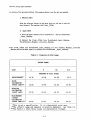
1
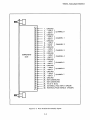
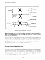
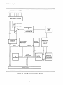
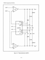
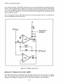
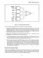
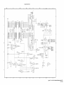
98640A Analog Input Interface
The data lines for the ADC are on pins 2 through 9. The output data bits are time multiplexed and
require two reads from the chip to get the full 12 bits of data. Three of the data lines (pins 7, 8, and
9) are also used as input lines to program the mode in which the converter operates.
The ADC is controlled by four control lines. The first is CHIP SELECT. Since the A -to-D chip is always selected, this line (pin 14) is tied to ground. The other three control lines are BUWR - (NOT buffered write), BURD- (NOT buffered read), and BUC/D- (buffered control/NOT data.) Signals for
these lines are generated by PROM U68 and buffered through filp-flop U67. (The signals generated
by the PROM are discussed in more detail later.) The system clock, SYCLK, is brought into the converter on pin I 3.
Four operations are carried out by the ADC chip:
Mod~9...&!"amming.
During this operation, the A-to-D card programs the A-to-D chip for 12-bit
unipolar output in straight binary coded form. To accomplish this programming, line BUWR - must
be low, lines BUC/D- and BURD- must be high, and the first three data lines must be low. The
control :signals come from the PROM (U68) via the flip-flop (U67); the data signals come from
BURD- through an inverting buffer (U 86).
Conver~.on. The conversion of the analog voltage to digital form starts when lines BUC/D- and
BUWR - go low. Once the conversion is started, it will run under control of the system clock until it
is complete; this takes 12.5 clock cycles. Since the digital conversion circuitry of the A-to-D card
runs on the same clock signals that the A-to-D chip uses, the digital circuitry simply waits an appropriatl~ number of clock cycles before requesting the results of the the conversion from the chip.
First.J!~..tuead. The ADC chip doesn't have enough data lines to output all of the data bits at once,
so two reads are needed to get the data out. The first read provides the 4 most significant bits of
converted data. This read occurs when BUC/D- and BUWR - are high and BURD- is low.
Secondjlatuead. The second data read provides the 8 least significant bits of converted data. This
happens when BUC/D- and BURD- are low and BUWR - is high.
Commc)n Mode Over range Detection
The common mode overrange detection circuit detects whether either of the op amps in the PGA is
producing an output that is greater than + 10 volts or less than -10 volts. The circuit uses 4 op amps
with open collectors, contained in package U 3 3.
The circuit works by comparing the outputs of the PGA op amps with the positive and negative voltage rails established in the input protection circuit. If one of the PGA op amps produces a voltage
grea ter in magnitude than 10 volts, one of the op amps in U 33 will detect it and turn on its open collector output, thus pulling the common mode overrange signal (OVD-) low. The state of the OVDsignal is provided in the 0 bit (bit 13) of the output data register.
DIGIT AL CONVERSION CIRCUITRY
The analog-to-digital conversions made by the A -to-D card are controlled by a state machine and associated digital circuitry. The next several paragraphs describe th~t circuitry in considerable detail.
3-13