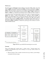
Download Paper - Asee peer logo
Transcript
AC 2009-527: LABORATORY CURRICULUM DEVELOPMENT USING RENESAS TECHNOLOGY Mukul Shirvaikar, University of Texas, Tyler Dr. Mukul Shirvaikar is the Chair and Professor of Electrical Engineering at the University of Texas at Tyler, where he develops curriculum and laboratories in computer engineering. Prior to this he worked at Texas Instruments specializing in real time imaging systems. Dr. Shirvaikar graduated with his doctorate from the University of Tennessee. He also has a M.S. degree from the University of Maine, and a B.Tech. from Banaras Hindu University, India. His current research interests include real time imaging and engineering education. Karthik Somaraju, University of Texas, Tyler Karthik Somaraju graduated with a Master's degree in Electrical Engineering from the University of Texas at Tyler in December 2008. He received his B.Tech. in Electronics and Communications from Jawaharlal Nehru Technological University. His other interests include microprocessors systems and software development. Page 14.829.1 © American Society for Engineering Education, 2009 Laboratory Curriculum Development using Renesas Technology Abstract This paper describes the laboratory curriculum developed for a junior-level introductory course in microprocessors for electrical engineering majors. The Bachelor of Science in Electrical Engineering (BSEE) curriculum has a required course in microprocessors and the prerequisites are courses in structured programming and digital systems. The laboratory procedures developed for this course are aimed at meeting the learning objectives of this course including assembly language programming, program debugging, serial communication, input/output devices, interrupts, interfacing, and direct memory access (DMA). The laboratory projects introduce students to the host–target environment using an integrated development environment (IDE). The platform currently utilized is a Freescale Semiconductor 68HC11 board produced by Axiom Manufacturing. The 68HC11 is a dated 8-bit architecture and has proved to be a robust platform to teach an introductory course. A new platform is currently being investigated for the microprocessor course partly enabled by an equipment grant from Renesas Inc. The lab projects were developed on the M16C/26A Quick Start Kit (QSK26A) supplied by Renesas Technology. The QSK26A board features on-board-in circuit debugging (ICD) and programming support, eliminating the use for an external ICD unit. The High-performance Embedded Workshop (HEW4) is a powerful real-time source-level debug environment supplied with the QSK26A. Apart from this, the Flash-over USB (FoUSB) programmer software allows in-system programming of the QSK26A board’s M16C/26A Flash MCU. An extensive set of manuals and technical literature is also available for the board. Some of the lab applications implemented in this project were: introduction to the M16C/26A, arithmetic operations, looping, subroutines, logical operations, LCD interface and application development (traffic signals). The lab projects are intended to give students a quick understanding of the instruction set, programming and operation of a microprocessor. A pilot lab is planned in the upcoming academic year. Page 14.829.2 Introduction A course on microprocessors is typically the central part of the curriculum in most Bachelor of Science in Electrical Engineering (BSEE) programs. This paper presents the laboratory curriculum developed for semester long junior-level introductory course in microprocessors. The lab projects were developed on the M16C/26A Quick Starter Kit (QSK26A) supplied by Renesas Technology1. Renesas Technology donated some sample QSK26A kits and software to the Department of Electrical Engineering through its university program. The lab projects developed for the QSK26A board assume that the students have at least one course in structured programming, and one course in digital systems, No prior experience with the operation of microprocessors is required. An extensive set of manuals and technical literature is also available for the board. The platform is ideally suited to expose students to microprocessors. The QSK26A board features on-board-in circuit debugging (ICD) and programming support, eliminating the use for an external ICD unit. QSK26A contains an installation CD-ROM that includes a complete Integrated Development Environment (IDE) called High-performance Embedded Workshop (HEW4). This is a powerful real-time source-level debug environment supplied with the QSK26A. This IDE contains the compiler, linker, assembler and debugger. Easy to use flash programming software called “Flash over USB (FoUSB)” allows the student to easily program the on-board flash. Figure 1 Renesas QSK26A Educational Board (adapted from Quick start guide for QSK26A1) Page 14.829.3 Past work Most electrical and computer engineering programs have a course in microprocessors with a laboratory component. These laboratory projects emphasize hands-on experience with computers and microprocessor technology. The students need to understand the basic relationship between assembly language for programming a microcomputer based system to allow the operation of the hardware2. Some commonly utilized hardware platforms for a microprocessor course are the Axiom CME12B/BC development board (populated with the Motorola MC68HC912B32 microcontroller)3, Motorola 68HC11EVB4, Intel 80865 and the Altera DE2 development and education board6. The platform currently utilized for this course is a Freescale Semiconductor 68HC11 board7 supplied by Axiom Inc. The 68HC11 is a dated 8-bit architecture and has proved to be a robust platform to teach an introductory course. The advantage is that it is a simple, mature platform that is cost effective and does not overwhelm the beginner8. However, it has several drawbacks that include an old serial interface, lack of a sophisticated IDE, limited debugging capability and the absence of a DMA controller on the chip. Most universities commonly use microprocessor lab projects such as arithmetic and logical operations on data values, interfacing with the hardware on the board and interrupt programming. MC68HC11 is still probably the most popular 8-bit microcontroller with enhancements to support an alphanumeric keyboard, multi-digit LED display and an alphanumeric CRT display to produce four rows of sixteen characters on standard video monitor. These I/O capabilities of MC68HC11 microcontroller are achieved with addition of minimum components9. Programs like TekBots10, a platform for learning created for electrical and computer engineering students will assist teaching many practical engineering skills including; innovation, design and real system problems. This platform gives the student experience as they use real hardware to see problems that can arise, allowing them to understand boards and systems. Page 14.829.4 A primary concern for any programming language course is the software development environment. One major advance in the IDE is the inclusion of plug-in compiler front-ends. This allows a single IDE to cover multiple source codes written in different programming languages completely transparent to the user and also allows a single IDE to be used to cover all levels of programming, from assembly language to other high level languages11. Basic topics like assembly-language programming, registers as ports or memory, interrupts and virtual machines require solid foundation built on simple initial ideas that later on can be understood with more detail12. Free versions like Microchip’s MPLAB Integrated Development Environment (IDE) and the datasheets for applicable Programmable Interface Controller (PIC) MCUs are easily accessible from Microchip’s website can be helpful for students to become familiar with the tools. Moreover, the labs, tutorials and exercises can be easily completed using the MPLAB SIM simulator13. Another such interesting platform is a racetrack platform along with the track, the microcontroller development board and microcontroller inputs and outputs. With this project students will gain experience with high-level microcontroller system concepts like interrupts as well as low-level concepts like assembly language programming, LED interfacing15. Microprocessor courses are typically taught using different microcontroller chips. This approach can be changed providing added educational benefits with the availability of field-programmable gate array (FPGA) and associated soft-core processors15. A new platform is currently being investigated for the microprocessor course partly enabled by an equipment grant from Renesas Inc. The major advantages of the new platform include sophisticated user friendly IDE, simple instructions set, ease of programming and DMA controller support. The lab projects developed using QSK26A board were: Introduction to M16C/26A, assembly language programming concepts, arithmetic and logic operations, general purpose output operations, general purpose input polling for switch input, introduction to interrupts and DMA transfer. Description of M16C/26A Renesas has a family of microcontrollers to address the market for various applications such as automatic motor control, digital home electronics, inverter application and networks. The M16C/26A is one of the many product offerings by Renesas in this domain. It is a 16-bit microcontroller with on board in-circuit debugger/programmer interface, 64K bytes user flash, A/D converter, 2 DMAC channels, 39 input/output (I/O) lines etc. The M16C/26A 48-pin version block diagram16 is shown in Figure 2. These single-chip microcomputers operate using sophisticated instructions featuring a high level of instruction efficiency. With 1M byte of address space, they are capable of executing instructions at high speed. In addition, this microcomputer contains a multiplier and a DMAC which combined with fast instruction processing capability, makes it suitable for control of various OA (operational amplifier), communication, and industrial equipment which requires high-speed arithmetic/logic operations. The variety of internal peripherals on the microcontroller reduces the need for external components. Its core has been designed to take advantage of the best features of register based architectures. The architecture makes it fast with efficient code execution. A hardware multiplier circuit and two DMAC’s are implemented to speed up the processing. Register configuration The following is a description of the register configuration for the M16C/26A. Page 14.829.5 ≠ Data registers: There are four 16-bit registers (of which two registers R0 and R1 can be used as 8-bit registers). For some instructions, registers R2 and R0 and registers R3 and R1 can be combined for use as 32-bit data registers (R2R0, R3R1), respectively. ≠ Address registers: Two 16-bit registers A0 and A1. For some instructions, registers A1 and A0 can be combined for use as a 32-bit address register (A1A0). ≠ Base registers: Two 16-bit registers frame base (FB) and stack base (SB). These registers consist of 16 bits each and are used in relative addressing. Figure 2 M16C/26A 48-pin version block diagram (adapted from M16C/26A group hardware manual16) ≠ Control registers / Program counter (PC): This counter consists of 20bits, indicating the address of an instruction to be executed. Page 14.829.6 / Interrupt table register (INTB): This register consists of 20 bits, indicating the start address of an interrupt vector table. / Stack pointers (USP, ISP): There are two stack pointers, a user stack pointer (USP) and an interrupt stack pointer (ISP) these are switched over by a stack pointer select flag (U flag). The U flag is assigned to seventh bit of the flag register (FLG). / Flag register (FLG): It consists of 11 bits, each of which is used as a flag. 1M-byte linear address space with relative jump instructions matched to distance of jump. Fast instruction execution times with shortest one-cycle instructions, 91 instructions include 20 onecycle instructions i.e. approximately 75% of instructions execute in five cycles or below. The M16C/26A programmer’s model contains thirteen 16-bit registers as shown in Figure 3 of these registers, R0, R1, R2, R3, A0, A1 and FB each consist of two register banks16. Figure 3 M16C/26A Programmer’s model Instruction set Page 14.829.7 The M16C/26A sample instructions are shown in Table 1. It has the familiar M16C 16-bit complex instruction set computer (CISC) register core architecture1. It allows for efficient program development with little memory capacity regardless of whether you are using assembly or C language. In addition some instructions can be executed in one clock cycle, making fast arithmetic processing possible. The instruction set also allows register-register, register-memory, memory-memory operations and arithmetic/logic operations on bits and 4-bit data16. M16C/26A have three major addressing modes; general addressing, special instruction addressing and bit instruction addressing. ≠ General instruction addressing accesses an area from 0000016 through 0FFFF16 and the following lists the name of each general instruction addressing mode: Immediate, register direct, absolute, address register indirect, address register relative, stack base relative, frame base relative and stack pointer relative. ≠ Special instruction addressing accesses an area from address 0000016 through FFFFF16 and control registers. The following lists the name of each specific instruction addressing mode: 20-bit absolute, address register relative with 20-bit displacement, 32-bit address register indirect, 32-bit register direct, control register direct and program counter relative. ≠ Bit instruction addressing accesses an area from address 0000016 through 0FFFF16 and the following lists the name of each bit instruction addressing mode: Register direct, absolute, address register indirect, address register relative, stack base relative, frame base relative. Some of the features of the multi-purpose instruction set are: ≠ Register and memory-indiscriminate instructions like MOV, ADD, SUB, etc. ≠ Powerful bit manipulation instructions like BNOT, BTST, BSET, etc. ≠ 4-bit transfer instructions such as MOVLL, MOVHL, etc. ≠ Normally used 1-byte instructions like MOV, ADD, SUB, JMP, etc. ≠ High-speed one-cycle instructions like MOV, ADD, SUB, etc. Page 14.829.8 Table 1 Sample Instruction set for the M16C/26A microcontroller Function Arithmetic Transfer Jump Mnemonic Op-code/format Description ABS ABS. size dest Absolute value ADC ADC. size src, dest Add with carry ADD ADD. size (:format) src, dest Add without carry CMP CMP. size (:format) src, dest Compare MUL MUL. size src, dest Signed multiply SUB SUB. size (:format) src, dest Subtract without borrow INC INC. size src, dest Increment DEC DEC. size dest Decrement MOV MOV. size (:format) src, dest Transfer POPM POPM dest Restore multiple registers PUSHA PUSHA src Save effective address LDE LDE. size src, dest Transfer from extended data area STNZ STNZ src, dest Conditional transfer XCHG XCHG. size src, dest Exchange JMP JMP (.length) label Unconditional jump JSR JSR (.length) label Subroutine call RTS RTS Return from subroutine ADJNZ ADJNZ. size src,dest,label Add and conditional jump SBJNZ SBJNZ. size src,dest,label Subtract and conditional jump INT INT src Interrupt by INT instruction PUSHC,POPC PUSHC src Save control register POPC dest Restore control register REIT Return from interrupt WAIT Wait NOP No operation BSET (:format) dest Set bit REIT Other WAIT NOP BSET Page 14.829.9 Memory map The memory map16 of M16C/26A is shown in Figure 4. It provides 1-Mbyte address space with addresses 0000016 through FFFFF16. The internal ROM is allocated at a high address, ending in address FFFFF16. For example, a 64-Kbyte internal ROM area is allocated in addresses F000016 to FFFFF16. The flash memory version got two sets of 2-Kbyte internal ROM area, block A and block B, for data space. These blocks are allocated addresses F00016 to FFFF16. The addresses FFFDC16 to FFFFF16 are allocated for fixed interrupt vectors and they store the start address of each interrupt routine. The internal RAM is allocated lower addresses, beginning with address 0040016. For example, a 1-Kbyte internal RAM area is allocated in addresses 0040016 to 007FF16. The internal RAM is used for storing data temporarily. The area is also used as stack when subroutines are called or interrupt requests are accepted. The SFR (special function registers) is allocated addresses 0000016 to 003FF16. The peripheral function control registers are allocated here. Blank spaces within SFR location are reserved and cannot be accessed by users. The addresses FFE0016 to FFFDB16 are allocated for special page vectors and they are used for JMPS and JSRS instruction. Figure 4 Memory map for M16C/26A including fixed vector table Interrupts There are 20 internal and 8 external sources, 4 software sources, 7 interrupt priority levels available for the M16C/26A 48-pin device. Interrupts are of two types namely software and hardware interrupts Hardware interrupts: These are further classified into two types namely: special interrupts and peripheral function interrupts. Page 14.829.10 ≠ / Special interrupts: These are non-maskable interrupts. Below are the following instructions that come under special interrupts: NMI, DBC, Watchdog timer, oscillation stop and re-oscillation detection, voltage down detection, single-step interrupt and address match interrupt. / Peripheral function interrupts: These are maskable interrupts generated by the microcomputer internal functions 16. ≠ Software interrupts: It occurs when executing certain instructions. These are nonmaskable interrupts. Following are the instructions that come under software interrupts: Undefined instruction (UND instruction), Overflow (INTO instruction), BRK instruction and INT instruction. Laboratory Environment The QSK26A comes with the M16C/26A board, USB power cord and QSK26A CD-ROM. In addition to the QSK26A it is necessary to have PC running a compatible Windows installation. As of this writing, Windows XP is recommended for the development environment. Other windows versions may be viable for the QSK26A development environment. The USB port connection between the board and the PC is used for allowing the host to directly issue the commands to the board and also acts as the power supply. High-performance Embedded Workshop (HEW) 17 The HEW is an integrated environment for debugging and development of embedded applications for Renesas microcontrollers. A microcontroller program is usually divided into multiple files to make it easier to read and understand. While exactly how the files are ordered is up to the programmer, typically the code is split into various files in a logical manner (e.g. math functions in one file, serial port drivers in another, etc.). After all the files in a project are compiled and assembled, a linker combines all the files into a single file. These steps can be tedious and repetitive. The Integrated Development Environment (IDE) called HEW simplifies the entire process. Some features of HEW include automatic generation of start-up code for every supported CPU, full simulation capability and comprehensive breakpoint functionality Figure 5 shows a screenshot of the HEW interface including the major tool windows that are typically utilized by the developer. Page 14.829.11 
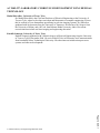
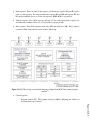
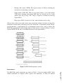
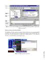
Figure 5 A screen shot of the High-performance Embedded Workshop (HEW) (adapted from HEW user manual20) Flash-over Universal Serial Bus (FoUSB) The FoUSB is a Windows application supplied by Renesas Technology for programming M16C flash MCUs. This application can be used along with the ICD to program the M16C MCU on a target board. After the compilation or assembly process, HEW generates a “.mot” format file. This file is used by FoUSB for programming the target. Page 14.829.12 Figure 6 FoUSB programmer application The FoUSB18 programmer software is also available as a standalone module shown in Figure 6. It can be used to reprogram the flash memory of a M16C/26A microcontroller over USB (universal serial bus). Laboratory Curriculum and Pedagogical Objectives The laboratory curriculum was designed to demonstrate several concepts necessary to meet the learning objectives for the microprocessor course. This was achieved by incorporating some simple application examples into each lab to demonstrate a principle. The lab projects developed using this board are summarized in Table 2. Table 2 General overview of lab projects Lab Title One Introduction to the M16C/26A Two Assembly Programming Concepts Three Arithmetic and Logic Operations Four General purpose output operations Five General purpose input Six Interrupts Seven Introduction to memory transfer using DMA Tools used Pedagogical Objectives HEW, Technical manuals, Understanding board FoUSB application functionality and software tools HEW, Assembly Looping, subroutines, language manual, startup swapping and comparing files of M16C/26A, the data in memory FoUSB application. locations or registers, observing the register and memory contents HEW, FoUSB Using the instruction set application, Software and for basic operations like Assembly language addition, subtraction and manuals multiplication. HEW, Software manual, Introduction to LCD FoUSB application interface, LED output and sorting data values in registers/memory locations HEW, MCU manuals, Controlling the blinking FoUSB application rate of LEDs and displaying the color of LED on LCD screen in accordance to the polling switch pressed HEW, MCU manuals, Introducing the concept of FoUSB application interrupts in M16C/26A HEW, MCU manuals, Transferring block of FoUSB application memory contents at once using DMA Page 14.829.13 The ABET course objectives for the course are enumerated below: By the end of this course students will be able to: 1. Understand basic microcomputer architecture 2. Program a microcomputer in assembly language 3. Design standard interfaces for microprocessors Lab 1 is an introduction to the QSK26A kit, HEW and FoUSB software development environment tools. The initial part of this lab demonstrates the way to create projects in HEW in assembly language. This lab familiarizes the student in using HEW tools understanding the file structure, type of files created during build process and settings made during a program execution. In the later part of the lab, students use a sample application program that is already included with the board. This application program demonstrates the use of hardware on the board like LEDs, switches etc. The students can modify some part of the written code to observe the change in the output. Lab 2 introduces assembly language programming concepts and the objectives are looping, subroutines, swapping and comparing the data in memory locations or registers. The students get to know how to observe the status of flags, instruction set and addressing modes being used. Lab 3 exposes the student to perform arithmetic, logical operations and understand how to modify data in registers and memory locations by writing their own program that executes arithmetic operations like addition, subtraction and multiplication. The students can set breakpoints in between their code and step through the program. This lab gives the student to show their programming skill and observe the necessary output windows like registers, RAM monitor window, memory map etc.,. Sample code and generated output values are shown in Figure 7. Page 14.829.14 Figure 7 Sample code and generated output values from Lab 3 Lab 4 is an introduction to general purpose output operations (LCD output) and also to apply sorting of data in memory locations in ascending or descending order. With this lab student will have an access to the hardware and can interface with LCD in printing their name or text on 8character 2-line LCD screen. In the later part of the lab students use a simple program to sort data consisting of a specified number of bytes in ascending order. Lab 5 is titled as general purpose input, polling for switch input. This lab is a step advance to fourth lab wherein students write a program to control the blinking rate of LEDs and display the polling switch pressed in accordance to the status of LEDs on the LCD screen. With this lab students will understand the concept of timers and interrupts. The desired programmed output on the QSK26A board is shown in Figure 8. (a) (b) Figure 8 The QSK26A a) LCD Module (adapted from schematics21) and b) Displaying output on LCD when switch is pressed Lab 6 and Lab 7 introduces the concept of interrupts and DMA8 transfer. With this lab, student gains an understanding of using interrupts in M16C/26A and how to register an interrupt in the interrupt vector table. The procedure consists of writing the interrupt handling functions and registering it to the interrupt vector table19. In addition, students will write a program to transfer the content of memory from one address to other every time a timer interrupt occurs. This makes use of two DMAC channels one to transfer from source to temporary RAM and other for a transfer from temporary RAM to the destination. All labs are to be written in assembly language; later labs have some C language. Conclusion Page 14.829.15 The laboratory curriculum developed will be piloted for the EENG 3307 Microprocessors course in Fall 2009. The lab projects are intended to give students a quick understanding of the instruction set, programming and operation of a microprocessor. This will also be useful for their senior design course as many projects utilize microprocessor/controller with interfacing circuitry for any given application. Based upon the experience further labs will incorporate applications such as keypad interfacing and automatic motor control for an advanced course in microprocessors that is being planned. Bibliography 1. 2. 3. 4. 5. 6. 7. 8. 9. 10. 11. 12. 13. 14. 15. 16. 17. 18. 19. 20. 21. Renesas Technology M16C/26A website, http://www.renesasuniversity.com/ Dorin Patru, Daniel B. Phillips and Eric Peskin, “A Two-Course Sequence in Computer Engineering Principles for Electrical Engineering Students” ASEE, 2007. “Microprocessor based system design lab”, http://www.eng.fsu.edu/ “Microprocessor systems”, http://www.ece.queensu.ca “Microprocessor systems”, http://www.doe.carleton.ca/~bmorshed/4601/ “Microprocessor labs”, http://coen.boisestate.edu/ Freescale Semiconductors 68HC11 board, http://www.freescale.com/ Ronald J. Tocci and Frank J. Ambrosio, “Microprocessors and Microcomputers”, 6th Edition, Prentice Hall, 2002. Christopher R. Carroll, Rocio Alba-Flores, Fernando Rios-Gutierrez, “New Life for the MC68HC11 Evaluation Board”, ASEE, 2002. Adriaan Smit, Donald Heer, Roger Traylor and Terri S. Fiez, “A Custom Microcontroller used as a platform for learning in ECE”, ASEE, 2004. Joerg Mossbrucker, “Using Embedded Systems to Teach all Levels of Programming to Electrical Engineering Students”, ASEE, 2006. Stephen C. Peterson, Alexandra Carey, Richard Hughey and David Meek, “Assembly Language Curriculum Realignment in Computer Engineering at UCSC”, ASEE, 2002. Marc McComb, “Online, Introductory Microcontroller Labs and Exercises for Engineering Students”, ASEE, 2008. Brinkley Sprunt, “A Novel Racetrack Platform For Teaching Microcontroller System Design Concepts”, ASEE, 2003. Arlen Planting and Sin Ming Loo, “On the Use of a Soft-core Processor in Junior Microprocessors Course”, ASEE, 2008. “M16C/26, M16C/26A, M16C/28, M16C/29 Group Hardware Manual and Software Manual”, Renesas Technology, 2002. “High-performance Embedded Workshop”, pp.1, Literature No.:REJ10J1737-0100, Renesas Technology, January 2005, http://documentation.renesas.com/. .”RTA-FoUSB-MON Flash Programmer and In-circuit debugger Users Manual”, Renesas Technology, 2003. “Interrupt handling in C Language”, Renesas Technology Application Notes, Literature No.: REJ05B08470100/Rev.1.00. January 2007 . “High-performance Embedded Workshop V.4.03 User’s manual”, Renesas Technology, pp.2, Literature No.:REJ10J1586-0100, April 2007. “QSK26A Schematics”, Renesas Technology, pp.3, Literature No.: RDECE_2662P_CR, August 2005. Page 14.829.16