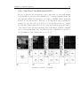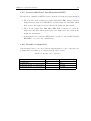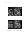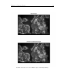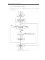
1
MASTER'S THESIS
Development of Vision Payload for the
Nanosatellite VELOX-I
Vineel Kumar Kadarla
Master of Science (120 credits)
Space Engineering - Space Master
Luleå University of Technology
Department of Computer Science, Electrical and Space Engineering
Development of Vision Payload for the
Nanosatellite VELOX-I
Vineel Kumar Kadarla
Supervisor
Assoc Prof Dr. Low Kay Soon
Satellite Research Center
[email protected]
Examiners
Dr. Anita Enmark
Division of Space Technology
[email protected]
Prof. Dr. Christophe Peymirat
Université Paul Sabatier
[email protected]
A thesis submitted in partial fulfillment for the Master of Science in
Space Science & Technology
Department of Computer Science, Electrical and Space Engineering
LuleåUniversity of Technology
November 2012
c Vineel Kadarla
Declaration of Authorship
I, Vineel Kumar Kadarla, declare that this thesis titled, ‘Development of Vision Payload
for Nano Satellite VELOX-I’ and the work presented in it are my own. I confirm that:
This work was done wholly or mainly while in candidature for a research degree
at this University.
Where I have consulted the published work of others, this is always clearly attributed.
Where I have quoted from the work of others, the source is always given. With
the exception of such quotations, this thesis is entirely my own work.
Signed:
Date:
i
“People don’t choose their careers; they are engulfed by them.”
John Dos Passos
LULEÅUNIVERSITY
Abstract
Division of Space Technology
Department of Computer Science, Electrical and Space Engineering
Master of Science
by Vineel Kumar Kadarla
In the recent years, CubeSat’s are evolving from purely educational tools to a standard
platform for technology demonstration and miniaturized scientific instrumentation. The
use of COTS (Commercial-Off-The-Shelf) components aided the ongoing miniaturization of several technologies and demonstrated successfully. Furthermore advantages in
this small satellite approach are due to their lesser development times and smaller sizes
suitable for multiple CubeSat launches on a single launcher into their respective designated orbits which is cost effective for Universities. These architectures not only promise
the combination of both temporal resolution of GEO missions with spatial resolution
of LEO missions, but also breaks the trade off in conventional Earth observation satellite designs. A thorough implementation of the firmware of vision payload of the Nano
Satellite VELOX-I for the Earth observation and remote sensing purposes, in the near
future with high scientific payoff is presented here. In course of implementation various
case studies have been learned, current date CCSDS recommendations for image compression have been considered. Effect of key components such as power, memory and
data transmission capability for small satellite remote sensing applications are discussed.
Implementation of the core firmware of the payload and serial interface development in
Java on Linux platform of Payload Processing Unit shall be able to inherit into the
future VELOX missions.
Acknowledgements
This thesis was conducted within VELOX program at Satellite Research Center, at
Nanyang Technological University. I would like to express my deep-felt gratitude to my
supervisor, Assoc Prof. Low Kay Soon (Director, Satellite Research Center) for providing me an opportunity. And would like to express my sincere thanks to Dr. Chen
Shoushun and his team for their support in providing me the necessary background information for the project. Jan P Hakenberg guidance and review in implementation of
project is exemplary. I would like to thank Project Managers Richard Bui and Lim Lip
San, academic coordinators Ms.Janet, Ms.Pamela and all other colleagues of Satellite
Research Center for their extensive support.
I am very grateful to my examiner, Dr. Anita Enmark for her supervision and acceptance of the topic for thesis work. I am deeply indebted to Space Master coordinator Dr.
Victoria Barabash, for her constant support in every instinct of my space master years.
I would extend my thanks to Dr. Johnny Ejemalm, Space Master thesis coordinator at
LTU and Prof. Christophe Peymirat at UPS for helping me out in the registration of
my thesis topic at respective Universities. I would like to extend my gratitude to Anette
Snällfot Brändström and Maria Winnebäck for their support in administrative issues
along my stay in Kiruna.
I would also like to thank all my friends, sister, cousin, my mom and dad for their
unconditional love, support in every new adventure i decide to start, and this thesis is
dedicated to all of them.
I want to give a special acknowledgement to the European Commission for Culture &
Exchange and the Space Masters consortium for the Erasmus Mundus scholarship that
allowed me to pursue studies.
Vineel Kumar Kadarla
iv
Contents
Declaration of Authorship
i
Abstract
iii
Acknowledgements
iv
List of Figures
viii
List of Tables
x
Abbreviations
xi
1 Introduction
1.1 Problem Statement . .
1.2 Research Objectives .
1.3 Structure of the Thesis
1.4 Work Methodology . .
.
.
.
.
.
.
.
.
.
.
.
.
.
.
.
.
.
.
.
.
.
.
.
.
.
.
.
.
.
.
.
.
.
.
.
.
.
.
.
.
.
.
.
.
.
.
.
.
.
.
.
.
.
.
.
.
.
.
.
.
1
2
2
3
4
2 Background
2.1 Nano Satellite Mission VELOX-I . . . . . . . . .
2.1.1 Mission Objectives . . . . . . . . . . . . .
2.1.2 Technical Facts . . . . . . . . . . . . . . .
2.2 Payload Architecture . . . . . . . . . . . . . . . .
2.2.1 Opal Kelly XEM3005 . . . . . . . . . . .
2.2.2 Radiation Hardened CMOS image sensor
2.2.3 Pluggable Processor Module (PPM) . . .
2.3 Optical System . . . . . . . . . . . . . . . . . . .
2.4 Operating System - Linux . . . . . . . . . . . . .
2.4.1 Internal Architecture . . . . . . . . . . . .
2.4.2 System Architecture . . . . . . . . . . . .
2.5 Programming Languages & Environment . . . . .
2.6 Software Design Methodology . . . . . . . . . . .
.
.
.
.
.
.
.
.
.
.
.
.
.
.
.
.
.
.
.
.
.
.
.
.
.
.
.
.
.
.
.
.
.
.
.
.
.
.
.
.
.
.
.
.
.
.
.
.
.
.
.
.
.
.
.
.
.
.
.
.
.
.
.
.
.
.
.
.
.
.
.
.
.
.
.
.
.
.
.
.
.
.
.
.
.
.
.
.
.
.
.
.
.
.
.
.
.
.
.
.
.
.
.
.
.
.
.
.
.
.
.
.
.
.
.
.
.
.
.
.
.
.
.
.
.
.
.
.
.
.
.
.
.
.
.
.
.
.
.
.
.
.
.
.
.
.
.
.
.
.
.
.
.
.
.
.
.
.
.
.
.
.
.
.
.
.
.
.
.
.
.
.
.
.
.
.
.
.
.
.
.
.
6
6
7
8
9
10
10
10
13
13
14
14
15
15
.
.
.
.
.
.
.
.
.
.
.
.
.
.
.
.
.
.
.
.
.
.
.
.
.
.
.
.
3 Literature Review
3.1 Digital representation of the images
v
.
.
.
.
.
.
.
.
.
.
.
.
.
.
.
.
.
.
.
.
.
.
.
.
.
.
.
.
17
. . . . . . . . . . . . . . . . . . . . . 17
Contents
vi
3.1.1
3.1.2
3.1.3
3.1.4
3.2
3.3
3.4
3.5
3.6
Integrated CMOS image Sensor . . . . . . . . .
Imager Facts . . . . . . . . . . . . . . . . . . .
Fill factor . . . . . . . . . . . . . . . . . . . . .
Noise . . . . . . . . . . . . . . . . . . . . . . .
3.1.4.1 Fixed Pattern Noise . . . . . . . . . .
3.1.5 Aspect Ratio . . . . . . . . . . . . . . . . . . .
Storage Capacity . . . . . . . . . . . . . . . . . . . . .
Image Compression . . . . . . . . . . . . . . . . . . . .
3.3.1 Types of redundancies . . . . . . . . . . . . . .
3.3.1.1 Coding Redundancy . . . . . . . . . .
3.3.1.2 Inter pixel Redundancy . . . . . . . .
3.3.1.3 Psycho-visual Redundancy . . . . . .
Measuring Image Information . . . . . . . . . . . . . .
Image Compression Model . . . . . . . . . . . . . . . .
Approach types . . . . . . . . . . . . . . . . . . . . . .
3.6.1 Error Metrics for Lossy Compression . . . . . .
3.6.2 Discrete Wavelet Transform based compression
3.6.2.1 9/7 Float Transform . . . . . . . . . .
3.6.2.2 Inverse 9/7 Float Transform . . . . .
3.6.3 Single-Level Two-Dimensional DWT . . . . . .
3.6.4 Multi-Level Two-Dimensional DWT . . . . . .
3.6.5 Inverse Multi-Level Two-Dimensional DWT . .
3.6.6 Results of compression . . . . . . . . . . . . . .
4 Firmware Development
4.1 System Configuration . . . . . . .
4.2 Programming Essentials . . . . . .
4.3 System Reset . . . . . . . . . . . .
4.4 Payload Initialization . . . . . . . .
4.5 Configurable Payload Parameters .
4.6 Main and Exposure Clocks . . . .
4.7 Exposure time . . . . . . . . . . .
4.8 GUI development . . . . . . . . . .
4.9 Image Acquisition . . . . . . . . .
4.10 Fixed Pattern Noise Cancellation .
4.11 CMOS Sensor Calibration . . . . .
4.11.1 Manual Calibrated Settings
4.11.2 Auto Calibration Settings .
4.12 Image Export & database . . . . .
.
.
.
.
.
.
.
.
.
.
.
.
.
.
.
.
.
.
.
.
.
.
.
.
.
.
.
.
.
.
.
.
.
.
.
.
.
.
.
.
.
.
5 Payload Interface Development
5.1 Introduction to Serial Port . . . . . . . .
5.1.1 Data Flow Speeds & Control . .
5.1.2 Character Framing . . . . . . . .
5.2 Serial programming for POSIX systems
5.2.1 Opening a Serial Port . . . . . .
5.2.2 Configuration the Serial Port . .
.
.
.
.
.
.
.
.
.
.
.
.
.
.
.
.
.
.
.
.
.
.
.
.
.
.
.
.
.
.
.
.
.
.
.
.
.
.
.
.
.
.
.
.
.
.
.
.
.
.
.
.
.
.
.
.
.
.
.
.
.
.
.
.
.
.
.
.
.
.
.
.
.
.
.
.
.
.
.
.
.
.
.
.
.
.
.
.
.
.
.
.
.
.
.
.
.
.
.
.
.
.
.
.
.
.
.
.
.
.
.
.
.
.
.
.
.
.
.
.
.
.
.
.
.
.
.
.
.
.
.
.
.
.
.
.
.
.
.
.
.
.
.
.
.
.
.
.
.
.
.
.
.
.
.
.
.
.
.
.
.
.
.
.
.
.
.
.
.
.
.
.
.
.
.
.
.
.
.
.
.
.
.
.
.
.
.
.
.
.
.
.
.
.
.
.
.
.
.
.
.
.
.
.
.
.
.
.
.
.
.
.
.
.
.
.
.
.
.
.
.
.
.
.
.
.
.
.
.
.
.
.
.
.
.
.
.
.
.
.
.
.
.
.
.
.
.
.
.
.
.
.
.
.
.
.
.
.
.
.
.
.
.
.
.
.
.
.
.
.
.
.
.
.
.
.
.
.
.
.
.
.
.
.
.
.
.
.
.
.
.
.
.
.
.
.
.
.
.
.
.
.
.
.
.
.
.
.
.
.
.
.
.
.
.
.
.
.
.
.
.
.
.
.
.
.
.
.
.
.
.
.
.
.
.
.
.
.
.
.
.
.
.
.
.
.
.
.
.
.
.
.
.
.
.
.
.
.
.
.
.
.
.
.
.
.
.
.
.
.
.
.
.
.
.
.
.
.
.
.
.
.
.
.
.
.
.
.
.
.
.
.
.
.
.
.
.
.
.
.
.
.
.
.
.
.
.
.
.
.
.
.
.
.
.
.
.
.
.
.
.
.
.
.
.
.
.
.
.
.
.
.
.
.
.
.
.
.
.
.
.
.
.
.
.
.
.
.
.
.
.
.
.
.
.
.
.
.
.
.
.
.
.
.
.
.
.
.
.
.
.
.
.
.
.
.
.
.
.
.
.
.
.
.
.
.
.
.
.
.
.
.
.
.
.
.
.
.
.
.
.
.
.
.
.
.
.
.
.
.
.
.
.
.
.
.
.
.
.
.
.
.
.
.
.
.
.
.
.
.
.
.
.
.
.
.
.
.
.
.
.
.
.
.
.
.
.
.
.
.
.
.
.
.
.
.
.
.
.
.
.
.
.
.
.
.
.
.
.
.
.
.
.
.
.
.
.
.
.
.
.
.
.
.
.
.
.
.
.
.
.
.
.
.
.
.
.
.
.
.
.
.
.
.
.
.
.
.
.
.
.
.
.
17
18
19
20
20
20
20
21
21
22
22
23
23
23
25
26
27
28
28
29
30
31
31
.
.
.
.
.
.
.
.
.
.
.
.
.
.
36
36
37
40
40
43
44
45
47
47
49
51
51
52
55
.
.
.
.
.
.
56
56
56
57
57
58
58
Contents
5.2.3
5.2.4
vii
Reading and Writing data onto the Port . . . . . . . . . . . . . . . 59
Closing a Serial Port . . . . . . . . . . . . . . . . . . . . . . . . . . 60
6 Image Handling Protocol
6.1 System Commands . . . . . . . . .
6.2 Camera Parameters . . . . . . . .
6.3 Listing the configured Parameters .
6.4 Trigger the Camera . . . . . . . . .
6.5 Deletion of the files . . . . . . . . .
6.6 Listing of the files . . . . . . . . .
6.7 Transfer of the file . . . . . . . . .
6.8 List the temperatures . . . . . . .
6.9 Halt the System . . . . . . . . . .
.
.
.
.
.
.
.
.
.
.
.
.
.
.
.
.
.
.
.
.
.
.
.
.
.
.
.
.
.
.
.
.
.
.
.
.
.
.
.
.
.
.
.
.
.
.
.
.
.
.
.
.
.
.
.
.
.
.
.
.
.
.
.
.
.
.
.
.
.
.
.
.
.
.
.
.
.
.
.
.
.
.
.
.
.
.
.
.
.
.
.
.
.
.
.
.
.
.
.
.
.
.
.
.
.
.
.
.
.
.
.
.
.
.
.
.
.
.
.
.
.
.
.
.
.
.
.
.
.
.
.
.
.
.
.
.
.
.
.
.
.
.
.
.
.
.
.
.
.
.
.
.
.
.
.
.
.
.
.
.
.
.
.
.
.
.
.
.
.
.
.
.
.
.
.
.
.
.
.
.
.
.
.
.
.
.
.
.
.
.
.
.
.
.
.
.
.
.
62
64
64
64
64
65
65
68
68
69
7 Conclusion & Future Work
70
7.1 Summary of the Thesis . . . . . . . . . . . . . . . . . . . . . . . . . . . . . 70
7.2 Future Work . . . . . . . . . . . . . . . . . . . . . . . . . . . . . . . . . . 70
A Linux Installation Procedure
72
B Missing Packages
B.1 Intel Network Packages . . . . . . . . . . . . . . . . .
B.2 Enable network interfaces . . . . . . . . . . . . . . . .
B.3 Locating the package repository . . . . . . . . . . . . .
B.4 To reload the rules in Ubuntu/Debian without restart
B.5 Enabling default root logging . . . . . . . . . . . . . .
74
74
75
75
76
76
.
.
.
.
.
.
.
.
.
.
.
.
.
.
.
.
.
.
.
.
.
.
.
.
.
.
.
.
.
.
.
.
.
.
.
.
.
.
.
.
.
.
.
.
.
.
.
.
.
.
.
.
.
.
.
C Specification Documents
77
Bibliography
79
List of Figures
1.1
Work Methodology . . . . . . . . . . . . . . . . . . . . . . . . . . . . . . .
2.1
2.2
2.3
2.4
2.5
2.6
2.7
2.8
2.9
2.10
2.11
2.12
2.13
Artistic impression of the Nano Satellite VELOX - I
Structure with Vision Payload . . . . . . . . . . . . .
Conceptual Payload Architecture . . . . . . . . . . .
Block Diagram of the Payload with interfaces . . . .
Opal Kelly XEM3005 architecture . . . . . . . . . .
Radiation Tolerant CMOS image sensor . . . . . . .
Internal Block diagram of SBC . . . . . . . . . . . .
Test optics of the Payload . . . . . . . . . . . . . . .
Linux Internal Architecture . . . . . . . . . . . . . .
Linux System Architecture . . . . . . . . . . . . . .
Implementation steps for small software packages . .
Implementation steps for large software packages . .
Iterative interaction between software design stages .
.
.
.
.
.
.
.
.
.
.
.
.
.
.
.
.
.
.
.
.
.
.
.
.
.
.
.
.
.
.
.
.
.
.
.
.
.
.
.
.
.
.
.
.
.
.
.
.
.
.
.
.
.
.
.
.
.
.
.
.
.
.
.
.
.
.
.
.
.
.
.
.
.
.
.
.
.
.
.
.
.
.
.
.
.
.
.
.
.
.
.
.
.
.
.
.
.
.
.
.
.
.
.
.
.
.
.
.
.
.
.
.
.
.
.
.
.
7
7
9
9
10
11
12
13
14
15
16
16
16
3.1
3.2
3.3
3.4
3.5
3.6
3.7
3.8
3.9
3.10
Digital representation of an image [1] . . . . . . . . . . . . .
Fill factor of the Pixel . . . . . . . . . . . . . . . . . . . . .
Image Compression Model . . . . . . . . . . . . . . . . . . .
Various compression techniques [2] . . . . . . . . . . . . . .
1D DWT . . . . . . . . . . . . . . . . . . . . . . . . . . . .
2D three level DWT . . . . . . . . . . . . . . . . . . . . . .
Original test image . . . . . . . . . . . . . . . . . . . . . . .
Result one level 2D DWT compared with Original Image .
Result two Level 2D DWT compared with Original Image .
Result three level 2D DWT compared with Original Image .
.
.
.
.
.
.
.
.
.
.
.
.
.
.
.
.
.
.
.
.
.
.
.
.
.
.
.
.
.
.
.
.
.
.
.
.
.
.
.
.
.
.
.
.
.
.
.
.
.
.
.
.
.
.
.
.
.
.
.
.
.
.
.
.
.
.
.
.
.
.
.
.
.
.
.
.
.
.
.
.
18
19
24
25
29
30
32
33
34
35
4.1
4.2
4.3
4.4
4.5
4.6
4.7
4.8
4.9
4.10
4.11
Image Sensor Board . . . . . . . . . . . .
Top Level Flow diagram . . . . . . . . . .
Class diagram for Payload Firmware . . .
Payload Initialization . . . . . . . . . . . .
Black Standard deviation . . . . . . . . .
Black Standard deviation . . . . . . . . .
Exposure time Vs mean gray-scale . . . .
Mean gray-scale Vs compressed image size
GUI for Vision Payload . . . . . . . . . .
Image Acquisition . . . . . . . . . . . . .
Recorded FPN from the Sensor . . . . . .
.
.
.
.
.
.
.
.
.
.
.
.
.
.
.
.
.
.
.
.
.
.
.
.
.
.
.
.
.
.
.
.
.
.
.
.
.
.
.
.
.
.
.
.
.
.
.
.
.
.
.
.
.
.
.
.
.
.
.
.
.
.
.
.
.
.
.
.
.
.
.
.
.
.
.
.
.
.
.
.
.
.
.
.
.
.
.
.
36
38
39
43
45
46
46
47
48
50
51
viii
.
.
.
.
.
.
.
.
.
.
.
.
.
.
.
.
.
.
.
.
.
.
.
.
.
.
.
.
.
.
.
.
.
.
.
.
.
.
.
.
.
.
.
.
.
.
.
.
.
.
.
.
.
.
.
.
.
.
.
.
.
.
.
.
.
.
.
.
.
.
.
.
.
.
.
.
.
.
.
.
.
.
.
.
.
.
.
.
.
.
.
.
.
.
.
.
.
.
.
.
.
.
.
.
.
.
.
.
.
.
.
.
.
.
.
.
.
.
.
.
.
.
.
.
.
.
.
.
.
.
.
.
.
.
.
.
.
.
.
.
.
.
.
.
.
.
.
.
.
5
List of Figures
ix
4.12
4.13
4.14
4.15
4.16
Auto Calibration . . . . . . . . . . . . . . . . . .
Image capture before sensor calibration . . . . .
Image capture after sensor auto calibration . . .
Image database structure . . . . . . . . . . . . .
Image database structure expanded for particular
. . .
. . .
. . .
. . .
slot
.
.
.
.
.
.
.
.
.
.
.
.
.
.
.
.
.
.
.
.
.
.
.
.
.
.
.
.
.
.
.
.
.
.
.
.
.
.
.
.
.
.
.
.
.
.
.
.
.
.
.
.
.
.
.
52
54
54
55
55
5.1
5.2
UART Serial [3] . . . . . . . . . . . . . . . . . . . . . . . . . . . . . . . . . 57
UART single byte frame . . . . . . . . . . . . . . . . . . . . . . . . . . . 57
6.1
Image Handling Flow diagram . . . . . . . . . . . . . . . . . . . . . . . . . 63
C.1 1U CubeSat Specifications . . . . . . . . . . . . . . . . . . . . . . . . . . . 77
C.2 3U CubeSat Specifications . . . . . . . . . . . . . . . . . . . . . . . . . . . 78
List of Tables
2.1
2.2
Facts: Nano Satellite VELOX -I . . . . . . . . . . . . . . . . . . . . . . . 8
Characteristics of the Optical lens . . . . . . . . . . . . . . . . . . . . . . 13
3.1
3.2
3.3
3.4
Loss less compression Vs Lossy compression
Filter Coefficients for 9/7 Float DWT [4] .
Filter Coefficients for 9/7 Float DWT [4] .
Results of the compression . . . . . . . . . .
4.1
4.2
4.3
Operational Mode . . . . . . . . . . . . . . . . . . . . . . . . . . . . . . . 36
Sensor Parameters . . . . . . . . . . . . . . . . . . . . . . . . . . . . . . . 37
Clock Values selection . . . . . . . . . . . . . . . . . . . . . . . . . . . . . 44
6.1
Reference Image Handling Protocol . . . . . . . . . . . . . . . . . . . . . . 67
x
.
.
.
.
.
.
.
.
.
.
.
.
.
.
.
.
.
.
.
.
.
.
.
.
.
.
.
.
.
.
.
.
.
.
.
.
.
.
.
.
.
.
.
.
.
.
.
.
.
.
.
.
.
.
.
.
.
.
.
.
.
.
.
.
.
.
.
.
26
28
28
31
Abbreviations
CMOS
Complementary Metal Oxide Semiconductor
DWT
Discrete Wavelet Transform
DPCM
Differential Pulse Code Modulation
FPGA
Field Programmable Gate Array
JPEG
Joint Photographic Experts Group
OBDH
Onboard Board Handling Unit
SBC
Single Board Computer
SaRC
Satellite Research Center
SNR
Signal to Noise Ratio
PPU
Pluggable Processor Unit
OBC
On Board Computer
LEO
Low Earth Orbit
GSD
Ground Sample Distance
COTS
Commercially Off The Shelf
CCSDS
Consultative Committee for Space Data Standards
xi
Dedicated to loving mom & dad
xii
Chapter 1
Introduction
Nano Satellite class of satellites is a proven cost effective approach for Earth observation missions with limitations of spatial resolution. 3U CubeSat which falls under this
class allow user to develop the various applications under the common bus architecture
based on COTS components. Generally, imaging systems are developed as an individual
sub system apart from the bus architecture owing to essential constraints like mass,
power, size, etc., in case of special segment of the Nano Satellite class, 3U CubeSat.
The main purpose of development of the vision payload is to capture the Earth images at an altitude 650 - 700 km, Sun synchronous low earth orbit (LEO) for remote
sensing application. Vision payload is developed as an individual subsystem, and shall
be integrated on to the Nano Satellite VELOX-I. Earth remote sensing helps in studying various phenomena related to Earth surface. The range of applications varies from
agriculture, geology, coast and marine studies to urban development and environmental
affairs. Remote sensing satellites are equipped with payload sensors that capture images
and aggregate data of Earth surface. The gathered information is then transmitted for
further processing and analysis. Satellite mission is one of the main factors that determines satellite overall dimensions, weight, and cost.[5] On the other hand, this limits
the final specifications to those of the components available in market. For instance,
the final Ground Sample Distance (GSD) is limited by the available commercial camera
systems, which usually do not meet dimensions and resolution requirements simultaneously. A better GSD can be achieved if a customized optical design is adopted besides
choosing off the shelf.
1
Chapter 1. Introduction
2
The payload comprises of three main modules:
• CMOS Sensor
• FPGA data acquisition board.
• Payload Processing Unit
In order to achieve the necessary (primary) objective of the payload i.e., to capture the
Earth images from such an altitude and the harsh environment, makes the payload to
consider the following absolute requirements.
• Radiation Environment:
XTo overcome the difficulty, a radiation tolerant CMOS sensor have been designed
and developed in house at Satellite Research Center, NTU.
• Optical Lens:
XIn order to satisfy the requirements of altitude and the ground sampling distance
of ∼ 70 meter, need for the design of optics is inevitable and manufacturing process
is outsourced.
1.1
Problem Statement
Most CubeSat employ a high resolution camera on-board and it is inevitable that the
images captured by the camera are larger than what can be sent to the ground station
in a single pass over the ground station. The purpose of Nano Satellite (VELOX-I) is
to capture images of the Earth and relay these images to the ground station with the
limited resources at hand. The focus of this research is to develop the firmware for the
full functionality of the vision payload and implement necessary compression algorithms,
and a detailed study on how these tasks are achieved without affecting the image quality
as well as a suitable design and firmware implementation is presented.
1.2
Research Objectives
The objective of this thesis is to develop the firmware for the vision payload for an Earth
observation Nano Satellite VELOX-I. In order to achieve the main objective, a number
of sub-objectives are identified and executed.
Chapter 1. Introduction
3
• Image Acquisition:
XInterfacing to the CMOS sensor to the Payload Processor Unit(PPU).
XControls of CMOS sensor parameters (exposure time, sensitivity, etc.,).
• Image Processing techniques:
XCompress images for better storage and transfer capability.
XEffective compression of the raw files.
XCreation of thumbnail of images captured.
• Serial Interface development:
XDevelopment of serial interface of the payload.
XDevelopment of Image/File handling protocol for tasks like trigger, file transfer,
deletion, etc.,
1.3
Structure of the Thesis
There are seven chapters presented in this thesis and their content are elucidated here
as follows.
Chapter 1 provides the introduction of the project, throws light on the problem statement, motivation behind the research work and justification of its relevance by means.
Chapter 2 contains the background information of the Nano Satellite mission, payload
architecture, tools used and software design methodology adopted during firmware development.
Chapter 3 explains the literature survey on issues that are relevant to development of
the payload. The survey starts with a discussion on digital representation of an image,
factors effecting the image acquisition, theory behind image compression and various
techniques available are presented. And first part of the thesis to investigate into viable
compression techniques based on the computational complexity and payload hardware
are studied, compression algorithms were implemented in MATLAB model and results
are presented.
Chapter 4 contains the second part of the thesis’ main contribution. This chapter starts
with the discussion of some key aspects of the payload development such as configuration of the CMOS Sensor via FPGA, various control parameters and artifacts of the
sensor design and overcoming of those by means of different calibration techniques are
presented. File handling structure, various storage formats and exporting of these are
explained with details.
Chapter 5 describes the payload interface development, introduction to the serial UART
interface and various parameters involved in configuring the serial port for the payload
are illustrated with necessary example codes.
Chapter 1. Introduction
4
Chapter 6 presents payload handling protocol developed with the help of the control
flow diagram, various functionality of payload are described under respective sections.
Chapter 7 concludes with the research outcome of the thesis, and suggests some possible
research work that can be done in the future to extend the outcome of present research.
1.4
Work Methodology
In order to achieve the expected results in prescribed definitive time line, the work plan
is divided into three phases, and is also represented by Figure [ 1.1]
1. Literature Review
In this phase, numerous similar implementations and their strategies in course of
development are studied and primary modules were implemented in MATLAB.
2. Design Phase
In this phase, a detailed software architecture which is backbone for the payload
firmware development is proposed.
3. Implementation, Integration & Test Phase
In this phase, the proposed software architecture in the earlier phase is implemented module by module, after implementation of the complete desired functionality software codes are integrated and progressively tested in order to avoid
system malfunctioning.
Chapter 1. Introduction
5
Submission of the thesis proposal Background Literature Review Design Phase System Level Design Documentation Top Level Design Application development Design Review Implementation, Integration & Test Phase Real time Test Master Thesis Figure 1.1: Work Methodology
Chapter 2
Background
A new class of Pico satellite, the CubeSat project began as a collaborative effort between
Prof. Jordi Puig Suari at California Polytechnic State University (Cal Poly), San Luis
Obispo, and Prof. Bob Twiggs at Stanford university in 1999. The main purpose of the
project is to provide a standard for design of pico satellites to reduce cost and development time, increase accessibility to space, and sustain frequent launches. A standard
one unit (1U) CubeSat occupies volume of 10x10x10 cm3 and weights no more than 1.3
kg. CubeSat, made from off the shelf components, provide a low cost platform and development time that is relatively small compared to conventional larger size satellites.[6]
Primary responsibility of the developers is to ensure the safety and success of CubeSat
missions hence they developed guidelines and the one who wants to develop the CubeSat must follow these guidelines. For all the above reasons companies, governmental
organizations, and universities expressed a growing interest in CubeSat as a low cost
mean of doing scientific space research missions and for testing and space qualification
of next generation of small payloads in space. Moreover, a CubeSat provides very useful
educating tools that train students and space engineers using real world satellite experience. 3U CubeSat is similar to 1U cube but has the dimensions of 30x10x10 cm3 and
weight not exceeding more than 4.5 kg.[5]
2.1
Nano Satellite Mission VELOX-I
VELOX-I is the first Singapore Nano Satellite to operate in LEO and is completely built
by students of Nanyang Technological University. Students participate in the projects
with the support from research students and staff. VELOX-I is planned to be launched
into the Low Earth Orbit in the second quarter of 2013. Attitude determination and
control system, power supply, and vision payload are developed in-house. The on-board
6
Chapter 2.Background
7
data handling and communication boards are commercially off-the-shelf hardware. The
scientific quantum payload will be developed by the Center for Quantum Technologies.
Ground Station for VHF/UHF bands has been built by NTU undergraduate students
and is operational since May 2010. [7]
Figure 2.1: Artistic impression of the Nano Satellite VELOX - I
Figure 2.2: Structure with Vision Payload
2.1.1
Mission Objectives
• To launch the first Singapore’s Nano Satellite VELOX-I. The satellite will be
designed, built, and operated by students from different schools in College of Engineering, NTU.
• To place and operate the satellite in a sun-synchronous LEO.
• To acquire images of Earth and transmit them back to ground station.
A narrow angle camera with tele-optics is used to provide high-resolution images
of Earth from LEO.
• To carry out experiments relevant to technology demonstration.
Payloads being studied: a vision system, a dual-FOV sun sensor and a quantum
physics payload.
Chapter 2.Background
2.1.2
8
Technical Facts
Table 2.1: Facts: Nano Satellite VELOX -I
Dimensions
Mass
Expected lifetime
Orbit
ADCS
OBDH Unit
Communications
Power subsystem
Structure
Thermal control
Ground segment
100 x 100 x 240 mm (N-Sat)
3500 g (N-Sat)
24 months
Sun-synchronous LEO, altitude 650 - 700 km
N-Sat: 3-axis stabilized and controlled: 1 GPS receiver,
2 sun sensors, 2 IMUs, 3 magnetic torquers, 3 reaction wheels;
1 OBC with Silicon Lab’s C8051F120 MCU
running data handling software on Salvo ROTS;
2GB SD card for data storage; UART and I2C data interfaces
Low gain antennas for Omni directional
coverage 1 dipole for UHF, 1 dipole for VHF;
UHF/VHF transceiver with AFSK modulation; 9600 bps
down-link / 1200 bps up-link, 1200 bps experimental
inter-satellite link
N-Sat: 4 deployable and 4 body-mounted 3J GaAs panels
for 19.2 W BOL power; 6.0 - 8.4 V unregulated,
latch-protected 5 V and 3.3 V bus;
3600 mAh Li-ion batteries
Hard anodized Al. 7075 chassis with
stainless steel load bearing parts;
Passive: Multi-Layer Insulation (MLI)
and radiators (N-Sat)
N-Sat: Vision system with extended optics
for ground sampling distance of 20 m
Ground station: NTU campus UHF/VHF high gain cross-yagi
antennas for TT&C and down-link
Chapter 2.Background
9
Figure 2.3: Conceptual Payload Architecture
Figure 2.4: Block Diagram of the Payload with interfaces
2.2
Payload Architecture
The arrangement of the three modules of the Payload are as shown in the virtual image
Figure 2.3 and its block diagram in the Figure {fig:block. The interface between these
modules can be seen in the Figure 2.4. Payload can be communicated with other devices
with Serial interface (UART) developed and CMOS image sensor configuration can be
loaded and accessed by the Xilinx FPGA module with USB interface.
Chapter 2.Background
2.2.1
10
Opal Kelly XEM3005
The Opal Kelly XEM3005-1200M32P is a compact 1,200,000-gate Xilinx Spartan-3E
FPGA board with 32MB RAM and USB 2.0 interface enabling an almost instant reprogramming of the FPGA makes us to choose this module for data acquisition from
the CMOS image sensor. It’s chosen for our project for being low cost. It is designed
without the power supply and that makes it better suits the end user design which is
required in our case. This device makes the Software / Hardware co-processing in our
case realizable.[8]
Figure 2.5: Opal Kelly XEM3005 architecture
2.2.2
Radiation Hardened CMOS image sensor
The Radiation tolerant image sensor chip layout for space application is as shown in
the Fig ??. The major design concerns lie within the design of the photo diode and
the floating diffusion node against radiation-induced dark current. In order to adapt
the sensor to the dramatic temperature change in space environment, a programmable
column biasing current circuit was considered in 4T pixel architecture of the sensor
design [9]
2.2.3
Pluggable Processor Module (PPM)
The Cool SpaceRunner-LX800 is a fully self-contained, rugged single board computer.
Its X86-compatible AMD Geode LX800 processor comes with graphics, 256MB RAM
and 2 GB solid state disk without any moving parts is as shown in the Fig 2.7. Either
VGA or LVDS displays are directly supported. All standard peripherals are already integrated on board. There is a LAN interface, four USB host ports, and two serial interfaces,
user configurable to handle either RS232 or RS485 levels.The Cool SpaceRunner-LX800
Chapter 2.Background
11
Figure 2.6: Radiation Tolerant CMOS image sensor
features status indication LED’s and a programmable watchdog. The computer can be
expanded with standard peripheral cards for the PC/104-Plus bus. This Single board
fan less computer is connected to the CMOS sensor interface board with PC/014-plus.
one of the USB port is connected to the XEM3005 FPGA module for CMOS sensor data
acquisition and operation.[10]
Power consumption is a mere 5 watts and doesn’t require cooling. The board is specified for the extended ambient temperature range of [-40
◦
C, +85
◦
C]. The Cool
SpaceRunner-LX800 uses the LiPPERT Enhanced Management Technology (LEMT).
It handles the boards housekeeping tasks like power sequencing and watchdog, and provides useful utility functions for the application. Among them is a secure, write and clear
protected Flash area that can be used for security keys. LEMT also enables remote condition monitoring. With its all the above features, the Cool SpaceRunner-LX800 is the
best choice for our purpose that need to operate in adverse environments. [10]
Chapter 2.Background
12
Figure 2.7: Internal Block diagram of SBC
Chapter 2.Background
13
Table 2.2: Characteristics of the Optical lens
Focal length
Maximum Aperture Ratio
Maximum Image Format
Operation Range Iris
Flange Back Length
Focus
Zoom
Object dimension at minimum object distance
2.3
3.5mm - 10.5mm
1:1.0
4.8mm x 3.6mm (diameter 6 mm)
F1.0 - F16C
12.5mm
0.3m - Inf
3.5mm - 10.5mm
3.5mm 52cm x 34.1cm
10.5mm 14.5cm x 10.8cm
Optical System
For Ground test purposes, we have chosen Computar T3Z3510CS-IR which has the
characteristics that are tabled in 2.2.
Figure 2.8: Test optics of the Payload
The lens system operates in both visible and IR regions of the light. The lens weights
63 grams. The diameter is 41.6mm, the height is 48.8mm. The lens is attached to the
PCB via CS-mount, and operates in temperatures between −20 ◦ C to 50 ◦ C.
2.4
Operating System - Linux
Linux is a free and open source computer operating systems distributed under open
source software license GNU General Public License. Linux was developed by Linus
Torvalds initially targeting Intel x86 based computer architectures, later ported to more
platforms than any other operating system. Linux due to its portability became predominant in embedded system developers. Linux kernel can be ported to both memory
and memory less embedded system devices. Many Linux distributions were available
til date, for our project purpose we have considered more popular and yet lite Debian
kernel for payload application development.
Chapter 2.Background
14
Figure 2.9: Linux Internal Architecture
2.4.1
Internal Architecture
The Linux operating system has unique architecture consists of kernel and shell as its
major components.
1. Shell: It is part of the operating system (OS), which serves as an intermediate
between the user and the OS.
2. Kernel: This serves as a direct interface between the hardware and the OS. Performs operations such as creation, deletion of the processes, scheduling of the process management. Provides the mechanisms for synchronization of the processes
and inter process communication.
2.4.2
System Architecture
The decomposition of the Linux Operating System can be as shown in the Figure 2.10
In Linux, everything is considered as a file other than the processes itself.
• User Applications: The user applications are developed in this layer.
• Operating System Services: These services are the part of the OS which also
provide interface to the Kernel.
Chapter 2.Background
15
Figure 2.10: Linux System Architecture
• Linux Kernel: The Linux Kernel abstracts and mediates access to the hardware
resources including the processor.
• Hardware Controllers: This sub-system consists of all the physical devices in the
Linux installation, devices such as Memory, Processor, USB drives and network
infrastructure.
2.5
Programming Languages & Environment
Application framework of the Payload is developed in Java, while the serial interface
developed in C/C++. In Course of sensor calibration, GUI has been developed in Java.
MATLAB is used for the validation of the Image Processing (compression) algorithms
as a proof of concept before implementation in the real time framework and also to
read raw image. Open source integrated development environment Eclipse is chosen for
firmware development on Linux due to its huge support from the developer’s community
and cross-platform compatibility.
2.6
Software Design Methodology
In order to achieve success in success in large software packages, some kind of strategy
or design methodology is mandatory. Essential steps of software development regardless
of size and complexity of the project are analysis and coding and is as shown in Figure
2.11. More Complex projects needed sophisticated approach with sections such as requirements capture in the preceding stage of analysis and followed by program design
and testing in the manner shown in 2.12. From the lessons learned, the implementation
of the methodology in Figure 2.12 may invite unnecessary risks an failure. Hence, an
iterative interaction between the development phases is appreciable and followed in this
project.
Chapter 2.Background
Figure 2.11: Implementation steps for small software packages
Figure 2.12: Implementation steps for large software packages
Figure 2.13: Iterative interaction between software design stages
16
Chapter 3
Literature Review
3.1
Digital representation of the images
An image may be defined as a two-dimensional function, f (x,y), where x and y are
spatial (plane) coordinates, and the amplitude of f at any pair of coordinates (x,y) is
called intensity or grey scale of the image at that point. When x,y and the intensity
values of f are all finite, discrete quantities, we call the image as digital image.[11]
A digital image f[m,n] described in a two-dimensional discrete space is derived from an
analog image f (x,y) in a continuous space through a sampling process that is termed
as digitization. A two-dimensional continuous image f (x,y) as shown in Fig 3.1 is
divided into N rows and M columns. And the intersection of the row and the column
is termed as pixel. In most cases, which we might consider to be the physical signal
that impinges on the face of a two-dimensional sensor, is actually a function of many
variables including depth (z), color (λ) and time (t). The value assigned to every pixel
is the average brightness in the pixel rounded to the nearest integer value. The process
of representing the amplitude of the two-dimensional signal at a given coordinate as an
integer value with L different gray levels is usually referred to as quantization [1].
3.1.1
Integrated CMOS image Sensor
Image sensors are manufactured in wafer foundries or fabs, these tiny circuits and devices
are etched onto silicon chips. The biggest problem with CCD is that there isn’t enough
economy of scale. They are created in foundries using specialized and expensive processes
that can only be used to make CCD. Today CMOS is the most common method for
manufacturing processors, image sensors and memories due to their high volume process
and low cost feature. There are two basic kind of CMOS image sensors available today.
17
Chapter 3. Literature Review
18
Figure 3.1: Digital representation of an image [1]
While these image sensors are inexpensive, they suffer from the Fixed Point Noise (FPN)
that resulted from each picture element having its own amplifier. Due to the unmatched
offset and gain characteristics between each amplifiers, they shall impose same noise
pattern on every image.
• Passive Pixel Sensors (PPS) were the first image-sensor devices used in the
1960s. In passive-pixel CMOS sensors, a photo site converts photons into an
electrical charge. This charge is then carried off the sensor and amplified. These
sensors are small and just large enough for the photo sites and their connections.
The problem with these sensors is noise that appears as a background pattern in
the image. To cancel out this noise, sensors often use additional processing steps.
• Active Pixel Sensor (APS) reduce the noise associated with passive-pixel sensors. Circuitry at each pixel determines what its noise level is and cancels it out.
It is this active circuitry that gives the active-pixel device its name. The performance of this technology is comparable to many charge-coupled devices (CCDs)
and also allows for a larger image array and higher resolution.[9]
3.1.2
Imager Facts
CMOS image sensors can incorporate other circuits on the same chip, eliminating the
many separate chips required for a CCD. This also allows additional on-chip features to
be added at little extra cost. These features include anti-jitters (image stabilization) and
image compression. Not only does this make the camera smaller, lighter, and cheaper;
it also requires less power so batteries last longer. It is technically feasible but not
economic to use the CCD manufacturing process to integrate other camera functions,
Chapter 3. Literature Review
19
such as the clock drivers, timing logic, and signal processing on the same chip as the
photo sites. These are normally put on separate chips so CCD cameras contain several
chips, often as many as 8, and not fewer than 3.CMOS image sensors can switch modes
on the fly between still photography and video. While CMOS sensors excel in the capture
of outdoor pictures on sunny days, they suffer in low light conditions. Their sensitivity
to light is decreased because part of each photo site is covered with circuitry that filters
out noise and performs other functions. The percentage of a pixel devoted to collecting
light is called the pixel’s fill factor. CCD’s have a 100% fill factor but CMOS cameras
have much less. The lower the fill factor, the less sensitive the sensor is and the longer
exposure times must be. Too low a fill factor makes indoor photography without a flash
virtually impossible. To compensate for lower fill-factors, micro-lenses can be added to
each pixel to gather light from the insensitive portions of the pixel and focus it down
to the photo site. In addition, the circuitry can be reduced so it doesn’t cover as large
an area. The quality of an image depends on the number of bits to represent an image,
more the number of bits more sharper the image. The radiation tolerant CMOS image
sensor developed in house at VIRTUS IC Design Center, NTU is of 12 bit.[9] [12]
3.1.3
Fill factor
Fill factor represents to the percentage of a photo site that is sensitive to light. Higher
the fill factor, higher sensitive to light and thus represents the good image sensor. In
the Fig 3.2, the photo detector represents the photo site that is sensitive to light and
the rest is the sensor circuitry.[9]
Figure 3.2: Fill factor of the Pixel
Chapter 3. Literature Review
3.1.4
20
Noise
Noise may be defined as an unwanted electrical signal that interferes with the image
being read and transferred by the image sensor. There are two types of noises generally
associated with the CMOS image sensors.
1. Read Noise: This noise is more generic random noise which is generated by the
noise characteristics of the associated electronics. This noise is also known as
temporal noise.
2. Fixed Pattern Noise: is a distortion that appears in an image due to variations of
device parameters across the sensor.
3.1.4.1
Fixed Pattern Noise
FPN effects the performance and quality of the image sensors, and usually refers to
non-temporal spatial noise which is due to device mismatch in pixels and color filters,
between the multiple gain amplifiers, ADC etc., FPN can be characterized as coherent
or non-coherent.
The most usual and hard noise in image sensors is associated with detectable row-wise
or column-wise artifacts which are due to mismatches in the multiple signal paths, and
un-correlated, row-wise operations in the image sensor. This type of noise is coherent
in nature and in general can be eliminated by reference frame subtraction.
Apart from the type of FPN discussed in earlier paragraph, most frequent FPN are dark
current FPN and FPN due to gain mismatches which are more difficult to remove as
the lead times to eliminate them are higher and dependent on the hardware.
3.1.5
Aspect Ratio
The ratio between the height and width of the sensor, derived from division of vertical
number of pixels(height) by horizontal number of pixels (width) leaving it in the fractional format.
Here in our case, 786 x 512 CMOS sensor would give an aspect ratio of 1.535 [9]
3.2
Storage Capacity
The imaging processing hardware of 3U CubeSat shall process the raw input image from
the payload through necessary steps such as filtering, compression and is stored. The
Chapter 3. Literature Review
21
output images, according to our mission requirements is store in memory of the SBC
which is in turn transferred to OBDH via serial interface and transmitted back to Earth.
This storage capability is not useful if the data rates are not increased accordingly. In
fact, it is trivial to show that there is a linear relationship between storage capability
and data rate if the constraint is enforced to have enough storage capability to store all
the images that can be downloaded in one access to the ground station:
Storage(M B) = 15/2δT (
min
)Rb (M bps)
access
(3.1)
where Storage(MB) is the storage capability required to be able to empty the memory
min
) is the average duration of
during one access to the ground station in MB; δT ( access
an access to the ground station in minutes, Rb (M bps) is the down-link data rate in
Mbps, and the factor
15
2
=
60
8
comes from transforming bits into bytes and minutes into
min
seconds. For Rb = 0.25 Mbps, and δT=5( access
), a storage capability of Storage(MB)=
9.3 MB is required, which is much lower than what can be achieved in CubeSat. It
follows that the real limiting factor is data rates, and not data storage. Furthermore,
we note that payloads that would have high requirements in terms of data storage such
as hyper-spectral image sensors are probably also incompatible with current CubeSat
technology because of other limitations, namely available power and space [13].
3.3
Image Compression
In general digital images need huge amount of space for their storage and require larger
bandwidths for transmission. The goal of the image compression is to reduce the amount
of data needed to represent the digital image. This in turn reduces amount of disk
space needed to store the image (in bytes) and improvises the disk capability to store
larger amounts of data. Further more it also lowers the bandwidth requirements in
transmission channels. 9/7 Wavelet filter based compression technique is chosen as
it is less computationally complex and targeted at Low powered devices (aka Small
Satellites). Ultimate choice was made due to the Nano Satellite mission constraints
(image quality, storage memory, bandwidth and power).[11]
3.3.1
Types of redundancies
Data compression aims to reduce the amount the data required to represent a given
quantity of information while preserving as much information as possible. Here, in the
definition data and information are not the same; data are the means by which the information is conveyed. The same information can be represented by various amounts of
Chapter 3. Literature Review
22
data which contain repetitive and irrelevant information are said to contain redundant
data.
If we let a and a’ denote the number of bits in two representations of the same information, the relative data redundancy R of the representation with a bits is
R=1−
1
C
(3.2)
where is C, is commonly called the compression ratio and is defined by
C=
a
a0
(3.3)
Image compression and coding techniques explore three types of redundancies : Coding
redundancy, Inter-pixel (spatial/temporal) redundancy and Psycho-visual redundancy.
3.3.1.1
Coding Redundancy
A code is a system of symbols (i.e.,bytes, bits) that represents information. Each piece
of information is represented by a set of code symbols. The gray level histogram of
an image can be used in construction of codes to reduce the data used to represent it.
Given the normalized histogram of a gray level image where
pr (rk ) =
nk
n
(3.4)
Where k = 0,1,2,..., L - 1, rk is the pixel values defined in the interval [0,1] and Pr(k) is
the probability of the occurrence of rk , L is the number of gray levels, nk is the number
of times that k th gray level appears and n is the total number of pixels. ??book)
Average number of bits used to represent each pixel is given by
Lavg =
L−1
X
l(rk )pr (rk )
(3.5)
k=0
3.3.1.2
Inter pixel Redundancy
The pixel values of an image are often correlated, there can be large spatial regions in
which the pixel values are clustered around the given intensity or color. Because of these
pixels when we try to encode the intensity of each pixel, the information is unnecessarily replicated in the representation of the neighboring pixels. The type of redundancy
that take form for images is spatial redundancy and for video it is temporal(or interframe)redundancy.Mapping technique is used in removal of inter-pixel redundancy and is
Chapter 3. Literature Review
23
a reversible process. Original image can be reconstructed from the transformed pixel values.Compression techniques such as CAC,(1-D, 2-D)Run Length Encoding techniques,
DPCM has inherent behavior of removal of inter-pixel redundancy.[11]
3.3.1.3
Psycho-visual Redundancy
Most 2-D intensity arrays contain information that is ignored by the human visual
system. So, compression techniques should aim in reducing the data that is psychovisually redundant.The elimination of this data is possible because the information itself
is not essential for visual processing but it leads to the omission of data with quantitative
information and is commonly referred to as quantization. This is an irreversible process
and leads to loss of image quality when reconstructed. Many compression techniques
exploit this type of redundancy. For instance, JPEG uses DCT of image pixel followed
by quantization of their coefficients. [11]
3.4
Measuring Image Information
The information in an image can be modeled as a probabilistic process, where we first
develop a statistical model of the image generation process. The information content
(entropy) can be estimated based on this model. The information per source (symbol
or pixel), which is also referred as entropy and is calculated by:
H=−
J
X
P (aj )logP (aj )
(3.6)
j=1
Where aj represent the source symbols, P (aj ) refers to the the source symbol / pixel
probability. J refers to the number of symbols or different pixel values.
3.5
Image Compression Model
An image compression system typically composed of two distinct functional components: an encoder and a decoder. Whereas the encoder performs the compression, and
the decoder performs the complementary operation to the earlier know as decompression. Both operations can be performed using software/hardware or the combination
of both firmware and hardware. For our mission criteria, we deploy the compression
algorithms in software.
Input image f(x,...) is fed into the encoder, which creates the compressed representation
Chapter 3. Literature Review
24
of the input, and when the compressed representation is presented to decoder,a reconstructed output of the input image f ’ (x,..) is generated. If the compression system
used is loss less, the reconstructed image is an exact replica of the original image.
Figure 3.3: Image Compression Model
The encoding compression process is elucidated here, the encoder in Fig 3.3 is designed
to remove the redundancies through a series of operations.
• Mapper: Transforms the f(x,..) into a format that reduces both spatial and
temporal redundancy. In general, mapping yields the first step of encoding process.
The mapping of an image into a set of less correlated transform coefficients.
• Quantizer: It reduces the accuracy of the mapper’s output in accordance to the
pre-established fidelity criteria. As the process is irreversible, it is omitted in
application where loss less compression are employed.
• Symbol Coder: It generates the fixed-length code to represent the output of the
quantizer and maps the output in accordance with the code.
The decoder in Fig 3.3 contains only two components namely, a symbol encoder
and an inverse mapper. They perform the exact inverse operation of the compression system. As the quantization results in the irreversible information loss,
we don’t include in the reconstruction process and is not included in the decoder
model.
Chapter 3. Literature Review
3.6
25
Approach types
Figure 3.4: Various compression techniques [2]
Fig 3.4 represents the classification of compression techniques of audio, video, and
image data. Most of the methods are waveform based. For image compression,
the two most widely used techniques are lossy and loss less compression techniques. Hence the subsequent sub-sections discuss lossy and loss less compression
techniques
Chapter 3. Literature Review
26
Table 3.1: Loss less compression Vs Lossy compression
Loss less Compression
Compression involves in exact replica
of the original data.
No Loss of quantitative information
Compression ratios are typically low,
hence require higher bit rates for transmission
Examples of usage: Medical data archiving,
text documents archiving where single errors
can damage the content a lot.
3.6.1
Lossy Compression
Compression involves in approximate
reconstruction when decompressed the
original data. Produces imperceptible losses
called as visually loss less
Loss of quantitative information
Higher compression ratios can be achievable,
requires low bit for transmission, but introduce
artifacts.
Mostly used in music and natural images,
used in cases where the errors are tolerable.
Error Metrics for Lossy Compression
For an original image A (x,y), the decompressed is given by A’ (x,y) where M, N
are the dimensions of the images respectively. Mainly two of the error metrics used
to compare the various compression techniques are Mean Square Error (MSE) and
the Mean Square Signal to Noise Ratio (SN Rms ). MSE is the cumulative square
error between the compressed and the original image and is given by
MSE =
1
MN
M X
N
X
[A(x, y) − A0 (x, y)]2
x=1 y=1
(SN Rms ) is a measure of the signal to the noise. For our case, we consider signal
as the original image and noise to the error in reconstruction of the image and is
given by
M X
N
X
(SNRms ) =
A0 (x, y)2
x=1 y=1
M X
N
X
[A(x, y) − A0 (x, y)]2
(3.7)
x=1 y=1
A compression scheme having the lower values of MSE and higher SNR is considered to be the better one.
Chapter 3. Literature Review
27
According to CCSDS recommended standards, data compression algorithm applied
to 2D digital spatial image data from payload instruments.
3.6.2
Discrete Wavelet Transform based compression
The current recommended standard makes use of a three-level, two dimensional
(2D), separable Discrete Wavelet Transform (DWT) with nine and seven taps for
low- and high-pass filters, respectively. Such a transform is produced by repeated
application of a one-dimensional (1D) DWT. Two specific 1D wavelets are specified
within this standard: [4]
1. The 9/7 bi orthogonal DWT, referred to as ‘9/7 Float DWT’
2. The ‘9/7 Integer DWT’ which is non-linear, integer approximation to the
earlier.
While the Float DWT generally exhibits superior compression efficiency in the
lossy domain, only the Integer DWT supports strictly loss less compression. Both
the compression schemes are assumed to use R-bit resolution, [R ≤ 16].
The values output from the 3-level 2D DWT are converted to appropriate integer
values before applying the Bit Plane Encoder. Each integer is represented using a
binary word consisting of a single sign bit along with several magnitude bits. The
maximum word size necessary to store each such integer depends on R. Whereas in
case of, the computed wavelet domain values are rounded to the respective nearest
integers before applying the BPE. A corresponding word length of R+5 bits is
adequate to store these integer values. In the case of the Integer DWT,the computed wavelet domain values are multiplied by integer weights that are uniform
in each sub band. A corresponding word length of R+4 bits is adequate to store
such integers before the weighting factors are applied. [4]
In our Project, we consider the 9/7 Float transform further for compression of the
satellite images.
Chapter 3. Literature Review
3.6.2.1
28
9/7 Float Transform
The 9/7 Float DWT uses two sets of analysis filter coefficients (’taps’), the numerical values of the filter taps are given in the table 3.2 along with their representations.
Table 3.2: Filter Coefficients for 9/7 Float DWT [4]
i
0
±1
±2
±3
4
3.6.2.2
Lowpass Filter hi
0.852698679009
0.377402855613
0.110624404418
0.023849465020
0.037828455507
Highpass Filter gi
-0.788485616406
0.418092273222
0.040689417609
0.064538882629
-
Inverse 9/7 Float Transform
The inverse 9/7 Float DWT uses two sets of synthesis filter coefficients,the numerical values of the filter taps are given in the table 3.2 along with their representations.
Table 3.3: Filter Coefficients for 9/7 Float DWT [4]
i
0
±1
±2
±3
4
Lowpass Filter qi
0.788485616406
0.418092273222
0.040689417609
0.064538882629
-
Highpass Filter pi
0.852698679009
0.377402855613
0.110624404418
0.023849465020
0.037828455507
Chapter 3. Literature Review
3.6.3
29
Single-Level Two-Dimensional DWT
Image de-correlation is accomplished using a two-dimensional DWT,by iteration
of 1D DWT. Viewing the image as a data matrix consisting of rows and columns
of signal vectors, a single-level 2D DWT shall be performed on the image in the
following two steps in the following order:
1. 1D DWT shall be performed on each image row, producing a horizontally
lowpass and a horizontally high-pass filtered intermediate data array, each
half as wide as the original image array, as illustrated in Fig 3.5 (b).
2. the 1-d DWT shall be applied to each column of both intermediate data
arrays to produce four sub bands as shown in Fig 3.5 (c).
Each of the four sub band data arrays obtained is half as wide and half as tall as
the original image array. In illustrations, these sub bands are often shown arranged
as one array which has the same size as the original image array, refer Fig 3.5 (c).
Starting at the upper left and proceeding clockwise in Fig 3.5 (c), the four sub
bands are referred to as LL, HL, HH, LH. [4]
Figure 3.5: 1D DWT
Chapter 3. Literature Review
3.6.4
30
Multi-Level Two-Dimensional DWT
In order to increase the effectiveness of the compression, we can apply further
levels if DWT decomposition and eliminate the correlation remaining in the LL
sub-bands after DWT decomposition. According to CCSDS, the recommended
levels of decomposition is three. This type of decomposition can be explained by
the Fig 3.6, the LL of the previous level of decomposition is used for further
decomposition. Each additional level of decomposition thus increases the number
of sub bands by three but leaves unchanged the total number of DWT coefficients
used to represent the image data. In general,n levels of 2D DWT decomposition,
the total number of sub bands is therefore 3n+1. [4]
Figure 3.6: 2D three level DWT
Chapter 3. Literature Review
3.6.5
31
Inverse Multi-Level Two-Dimensional DWT
The inversion of multi-level DWT is carried out in the following steps sequentially.[4]
1. The four sub bands of highest level, LL3, LH3, HL3, HH3, shall be inverted
using an inverse single-level 2D DWT to yield the single sub band LL2, which
then replaces the higher-level sub bands in the transform data matrix.
2. The four sub bands LL2, LH2, HL2, HH2 shall be inverted to yield the
single sub band LL1, which again replaces the higher-level sub bands in the
transform data matrix.
3. A final single-level 2-d inverse DWT shall be applied to sub bands LL1, LH1,
HL1,HH1 to reproduce the original image.
3.6.6
Results of compression
Various images have been tested with the implementation of the compression algorithm and best results are documented in the table 3.4 here.
Table 3.4: Results of the compression
Parameter
Row Size
Column Size
Compression ratio for 1-Level(%)
Compression ratio for 3-Level(%)
Original Image
512
768
1
1
Compressed Image
512
768
27.0805
50.1201
Chapter 3. Literature Review
Figure 3.7: Original test image
32
Chapter 3. Literature Review
Figure 3.8: Result one level 2D DWT compared with Original Image
33
Chapter 3. Literature Review
Figure 3.9: Result two Level 2D DWT compared with Original Image
34
Chapter 3. Literature Review
Figure 3.10: Result three level 2D DWT compared with Original Image
35
Chapter 4
Firmware Development
4.1
System Configuration
The Vision Payload of Nano Satellite VELOX - I, comprises of a radiation hardened CMOS image sensor which works in array mode. Pixel arrangement in this
mode size are given in the table 4.1. In array scan mode, pixels are arranged in
768 x 512 pattern can be seen in the Figure below 4.1
Parameter
Operational Mode
Pixel Size
Pixel Array
Type
Array Mode
6.5 µm x 6.5 µm
768 x 512
Table 4.1: Operational Mode
The image captured using the above sensor depends on the different parameters
slated in the table 4.2 given below.
Figure 4.1: Image Sensor Board
36
Chapter 4. Firmware Development
Quantity
Exposure time
Readout time
Gain
Vref
37
Description
Time for which light is exposed to the pixels.
Exposure times are directly proportional to pixel
output.
Time in which output is read from all the pixels.
The amplification factor for the voltage perceived
before processing.
Vref values at ADC conversion phase, right
balance between the values avoids image extreme
darkening / brightening of the image
Table 4.2: Sensor Parameters
In order to capture the image from the Payload, two main arguments are to be
passed via serial interface ie., they are the slot ID to which the captured files are
stored in the SSD memory and the mode of operation of the payload. The first
and foremost argument is slot ID. slot ID 254 and 255 are not taken as arguments,
these are reserved for specific purposes. One for the random image creation to
test the payload functionality and the later to the standard image stored at the
time of integration & assembly. Second most important parameter is the mode
of operation of the Payload. The mode of operation depends on whether Vref is
zero or not. For the true condition, payload is auto calibrated otherwise image is
captured. After successful completion of either conditions, function returns to the
main and waits for the serial command.
4.2
Programming Essentials
In order to program and execute the Payload firmware, it is to be checked whether
the shared libraries are copied into proper location usr/lib. Device acceptance
rules for FPGA module should be reloaded with commands as in Appendix B.
The Linux installation requires the addition of one file to the directory:
60-opalkelly.rules -----> /etc/udev/rules.d/
This file includes a generic udev rule to set the permissions on all attached Opal
Kelly USB devices to allow user access. Once this file is in place, you will need to
reload the rules by either rebooting or using the following command:
/sbin/udevcontrol reload rules
With these files in place, the Linux device system should automatically provide
write permissions to XEM devices attached to the USB.
For usage of Java API in Linux,
Chapter 4. Firmware Development
38
Figure 4.2: Top Level Flow diagram
libokjFrontPanel.so needs to be copied to the java.library.path.
On Debian, you can copy it to /usr/lib/jvm/jre/lib/i386
okjFrontPanel.jar should be added to your CLASSPATH. It can either be uncompressed or referred to directly on the javac/java command lines as below.
To build and run ImageAcquisition.java:
javac -classpath okjFrontPanel.jar ImageAcquisition.java
java -classpath .:okjFrontPanel.jar ImageAcquisition e inputfile outputfile
The class diagram for the entire payload firmware is as shown in the Figure 4.3
Chapter 4. Firmware Development
Figure 4.3: Class diagram for Payload Firmware
39
Chapter 4. Firmware Development
4.3
40
System Reset
Performs a reset of the FPGA internals. This requires that FrontPanel support
be present in the FPGA design because the reset signal actually comes from the
FrontPanel Host Interface (application).
if (myErrorCode.equals(ErrorCode.NoError))
public static final int soft reset addr = 0x0f;
public static final int sensor ctrl addr = 0x00;
myOkFrontPanel.SetWireInValue(soft reset addr, 0x8000, 0x8000);
myOkFrontPanel.UpdateWireIns();
myOkFrontPanel.SetWireInValue(soft reset addr, 0x0000, 0x8000);
myOkFrontPanel.UpdateWireIns();
myOkFrontPanel.SetWireInValue(sensor ctrl addr,
mySensorControl.getCMOSvalue(), 0xfffe);
myOkFrontPanel.UpdateWireIns();
Wire In endpoint values are stored internally and updated when necessary by
calling (UpdateWireIns(). The values are updated on every endpoint basis by
calling this method. In addition, specific bits may be updated independent of
other bits within an endpoint by using the optional mask. This method is called
after all Wire In values have been updated using SetWireInValue(). The latter
call merely updates the values held within a data structure inside the class. This
method actually commits the changes to the XEM simultaneously so that all wires
will be updated at the same time.
4.4
Payload Initialization
The FrontPanel API provides a powerful C++ interface to Opal Kelly USB boards.
To build an application using this API, one should include the files okFrontPanelDLL.h and okFrontPanelDLL.cpp in the project if programmed in C/C++.
These files contain stub functions that call to the DLL or Shared Libraries (in case
of Linux). In our case, as the application framework is developed in Java on Linux
Single Board Computer(SBC), we should also include shared library object files
Chapter 4. Firmware Development
41
during run time termed as ‘libokjFrontPanel.so’ and it is also mandatory to export
their path and specify at the time of compilation. To use the library, you create
an instance of myOkFrontPanel which encapsulates communication with the USB
driver and provides access to FrontPanel endpoints. Initialization is as shown in
the Figure 4.4
Firstly, libraries are to be loaded and an instance is created for checking the system
error codes by,
System.loadLibrary("okjFrontPanel");
ErrorCode myErrorCode;
An instance of the okFrontPanel created in the application by,
okFrontPanel myOkFrontPanel
myOkFrontPanel = new okFrontPanel();
Here, myOkFrontPanel will be referred as a class whenever its sub functions are
needed to be utilized in the application.
Secondly, the computer needs to scan for the XEM model which it is about to
communicate.An empty string variable needs to be declared to store the device
serial number, which will be used to open the device. The sequence of commands
is:
System.out.println("OpenBySerial:" + myErrorCode);
System.out.println("GetDeviceCount:" + myOkFrontPanel.GetDeviceCount());
BoardModel myBoardModel = myOkFrontPanel.GetDeviceListModel(0);
System.out.println("BoardModel:" + myBoardModel.toString());
System.out.println("DeviceID:" + myOkFrontPanel.GetDeviceID());
This retrieves the serial number of the first connected device, depicted by the
integer ‘0’, and stores it in a string myErrorCode, which will be used in the
OpenBySerial function of the myErrorCode class. Besides the retrieving the serial
number of the device, additional commands are used to retrieve the number of devices connected and their respective board models for the user’s reference during
application development.
BoardModel myBoardModel = myOkFrontPanel.GetDeviceListModel(0);
System.out.println("BoardModel:" + myBoardModel.toString());
The command returns an integer relating to the first scanned XEM device, which
Chapter 4. Firmware Development
42
subsequently needs to be referred to a lookup table containing the corresponding
device models. After storing the data into the variables, appropriate combinations
of switch(case) gains access for different functions from the serial interface.
Thirdly, PLL has to be configured with the set the commands defined in the data
sheet of cypress semiconductor and the Opal Kelly user manual [8] [14].
Create an instance for PLL by,
myOkPLL22150 = new okPLL22150();
myOkPLL22150.SetReference(48.0f, false);
// default PLL settings, Vref=48Mhz, fixed for CY22150
myOkPLL22150.SetVCOParameters(400, 48);
// VCO=48*400/48=400Mhz, DO NOT CHANGE THIS.
myOkPLL22150.SetDiv2(DividerSource.DivSrc VCO, 20);
// VCO,DIV2N=20.
Div2ByN =400/20 = 20MHz
myOkPLL22150.SetOutputSource(0, ClockSource.ClkSrc Div2By4);
// 400/4 = 100MHz.
for SDRAM
myOkPLL22150.SetOutputEnable(0, true);
myOkPLL22150.SetOutputSource(2, ClockSource.ClkSrc Div2ByN);
// Div2ByN =400/20 = 20MHz
myOkPLL22150.SetOutputEnable(2, true); // Div2ByN for exposure clock
// disable other clock outputs
myOkPLL22150.SetDiv1(DividerSource.DivSrc VCO, 20);
// divider1:
input,VCO,DIV1N=20.
Div1ByN = 400/20=20MHz
myOkPLL22150.SetOutputSource(1, ClockSource.ClkSrc Div1ByN);
// Div1ByN for main clock (sensor, ADC)
myOkPLL22150.SetOutputEnable(1, true);
myOkPLL22150.SetOutputEnable(3, false);
myOkPLL22150.SetOutputEnable(4, false);
myOkPLL22150.SetOutputEnable(5, false);
return myOkFrontPanel.SetPLL22150Configuration(myOkPLL22150);
Finally, a configuration file is loaded into the FPGA. This configuration file is generated from the Xilinx ISE software, which contains the digital blocks programmed
in VHDL.
myErrorCode = myOkFrontPanel.ConfigureFPGA("get/bin/top.bit");
The above example loads the configuration file named ‘top.bit’ into the FPGA.
This also returns an integer value which indicates whether the configuration is
Chapter 4. Firmware Development
43
Figure 4.4: Payload Initialization
successful. For a no error case, the returned value is 0.
4.5
Configurable Payload Parameters
The Payload can be configured with variable key parameters that effect the image
quality, list of such parameters are shown here. These parameters can be configured via UART serial interface protocol defined in the Chapter 6 in this thesis.
Chapter 4. Firmware Development
44
Table 4.3: Clock Values selection
Register Value
30
31
32
33
34
35
36
37
38
39
40
Effective Frequency [MHz]
13.333333
12.903226
12.5
12.121212
11.764706
11.428572
11.111111
10.810811
10.526316
10.256411
10.0
These parameters are configured with arguments (min,max,value) and some typical values for test have be shown here as an example.
array exposure cnt(0, 1023, 1023),
main clk(1, 40, 25),
exposure clk(1, 40, 31),
cds gain(0, 3, 1),
probe select(0, 1, 1),
vref(0, 255, 127),
stretch lo(0, 4096, 506),
stretch hi(0, 4096, 2956);
These parameters are once initially configured in the from the serial interface
later on the configuration is stored in ‘campar.bin’ and accessed whenever the
configuration is changed depending on the region of interest that is to be captured.
4.6
Main and Exposure Clocks
The main clock provides the timer to the FPGA. Clock register value determine
the quality of the image and for this sensor they are observed in the range of 30-40.
We perform the following experiment: The lens is covered with a lid to prevent
the exposure of the CMOS sensor to light. Then, we sweep through all possible
pairs of clock values, taking 20 exposures for each tuple. We average the images
for each clock value tuple and form the distribution of gray-scale values, as well as
correlation of adjacent pixels.
Chapter 4. Firmware Development
45
Figure 4.5: Black Standard deviation
The results are shown in Figure 4.5 and Figure 4.6. The noise distribution varies
significantly with the choice of clock values.
– To minimize the pixel noise variance, the main clock register should range
between 35 - 38.
– To maximize the correlation of the vertical adjacent pixels, the main clock
register should be set to 35, 37, or 40.
– To maximize the correlation of the horizontal adjacent pixels, the main clock
and exposure clock values can be selected from the list: (35,32), (36,38), (37,
40), (38, 39), (39, 37), ..., (40, 36).
For our final algorithm, we combines these rules of thumb. We have distilled a
list of clock value register tuples that the exposure mechanism chooses randomly
from. In the firmware (40, 39), (39, 34), (39, 32), (37, 40), (37, 39), (37, 38), (37,
32), (36, 40), (36, 39), (36, 38), (36, 37), (36, 36), (35, 32).
4.7
Exposure time
Exposure time has the great impact on image quality as they affects the contrast of
an image. Typically, an image with good contrast values has a spread distribution
of gray-scale values.
– If the exposure time is too small, the image exhibits mostly dark pixels.
– If the exposure time is too large, the image exhibits mostly white pixels
In order to obtain an image with good contrast, the exposure time needs to be
chosen just right. The exposure time does not relate to average intensity, i.e. mean
gray-scale, in a linear fashion. Our experiments suggest, that for each scene, there
is a region on the exposure time logarithmic scale, where the average intensity increases linearly. Once the average intensity approaches a limit, it does not increase
significantly anymore.
Chapter 4. Firmware Development
Figure 4.6: Black Standard deviation
Figure 4.7: Exposure time Vs mean gray-scale
46
Chapter 4. Firmware Development
47
Figure 4.8: Mean gray-scale Vs compressed image size
Above, we mentioned that the average intensity should ideally be medium gray. In
order to back that claim, we evaluate the file sizes of the images in their compressed
format. A low file size means, little information remains in the image, when
compared to an image of the same scene with a larger file size. Our experiments
suggest that the maximum file size is not obtained at the exact medium intensity,
i.e. 50% gray-scale, but above that value namely around 60% gray-scale value.
The results of this observation can be shown in Figures 4.7 and Figure 4.8.
4.8
GUI development
Graphical User Interface is developed in order to experiment the Sensor quality and
faster configuration of key parameters. Images are captured at different instants
with varying configurable parameters. Screen shot of the GUI developed can be
seen in the Figure 4.9. The sliders in the GUI with key configurable parameters
can be adjusted to their (minima,maxima) limits programmed earlier.
4.9
Image Acquisition
During the sensor configuration, the configurable parameters stored in campar.bin
are stored in global variables. For the Readout and Exposure clocks, the respective PLL [14] will be configured immediately after the file is parsed and read.
Chapter 4. Firmware Development
48
Figure 4.9: GUI for Vision Payload
These parameters are sent to the FPGA for configuration. These variables will
be processed in various sub functions in the program, before sending the updated
configuration parameters to the FPGA The image acquisition operation can be performed anytime after the successful configuration of the sensor & FPGA. Taking
reference from the these values, sensor configuration is set and the corresponding
image with respect to the mode of operation and number of slot to store the captured image is processed. Next, the data for the Fixed Pattern Noise (FPN) is
loaded and stored in an FPN buffer myByteBuffer2, details on how the FPN values
are obtained will be discussed in the later section. The digitized raw data of the
image is then read from the SDRAM and stored in another buffer myByteBuffer
using the ReadFromBlockPipeOut() function explained earlier. Noise cancellation
of the data is performed by subtracting the FPN values from the obtained raw
data and the new image without noise is obtained. As these values are in 12 bits,
the operations have to be done on a high byte and a low byte, which requires 2
elements for both arrays. Thus bit shifting operations and address assignments
to the values have to be performed during the noise cancellation. In addition,
the obtained values after noise cancellation cannot be outside the 12 bit (0-4095)
range. These values will be set to the corresponding minimum or maximum values. The algorithm is shown below, where by a for loop is called with the number
of pixels set as a loop count (c0) limit . The retrieved values from the FPGA,
stored in myByteBuffer, is being subtracted with the myByteBuffer2. The higher
bytes of the 2 arrays are multiplied by 256, which is equivalent to an 8 bit left
shift, while the lower bytes are kept at their original value. After the computation,
the final value is stored in the variable myInt, which will be processed to set all
Chapter 4. Firmware Development
49
values below 0 to be 0, and values above 4095 to be 4095. Finally, the individual
buff val will be separated into 2 bytes, storing them at 2 separate locations in the
sdram buffer array. Appropriate masking and bit shifting operations are used to
ensure the values are correct.
After the noise cancellation operation, the data is further mapped into 8 bits using a set of limits. Similarly, the values outside the limits will be set to either
0 or 255, while the rest will be normalized to their equivalent 8 bit value. The
algorithm shown below processes the similar buff value obtained earlier. The 8 bit
normalization limits are determined by global variables strech lo and strech hi,
whereby values exceeding the limits will be set as 0 for the lower limit and 255 for
the upper limit. The values within range will be normalized by proportion. The
arrays which contain the image information will be subsequently saved in a binary
format file.
After Successful initialization of the Payload, a raw image is stored in the myByteBuffer via routine getRaw(). A condition is introduced to check whether the
image is created or not, TRUE succeeds importing of FPN buffer image to the
myByteBuffer2. New image is produced after cancellation of the Fixed Pattern
Noise. Further image is down scaled from 12 bit resolution to 8 bit and stored in
the external folder Image Container in our case for further operations on board
of the satellite like thumbnail creation, compression, filtering etc., Process can be
explained with the control flow diagram in 4.10.
4.10
Fixed Pattern Noise Cancellation
The FPN noise is the pixel noise generated when the camera is in operation,
whereby particular pixels are susceptible to giving brighter intensities above the
general background noise. The pixel layout of the camera sensor forms patters
of 16 columns of pixels, which resulted in a pattern of vertical lines appearing
on the image. After applying a reference setting (Readout Clk, Exposure Clk,
Array Mode Exposure Count) on the camera, the FPN noise is captured when the
aperture of lens is closed and saved for further processing in removal of the noise.
Vref is adjusted such that the digitized values of the pixel noise are not too high
or too low to perform noise cancellation. If the noise values are too high for noise
cancellation, an image will not be formed due to the low resultant bit values after
cancellation. If the noise values are too low, the vertical lines will still be visibly
prominent in the image. The mean of the digitized 12 bit voltage is monitored in
the GUI upon image capture. white piece of paper is used as an image reference to
determine whether the noise is still visible after noise cancellation.Fixed pixel bias
Chapter 4. Firmware Development
Figure 4.10: Image Acquisition
50
Chapter 4. Firmware Development
51
denotes the average intensity perceived by the pixel location when the exposure
occurs in total darkness. In total darkness, all pixels should ideally read out
identical values (since the light intensity is the same for all pixels). However, due
to irregularities in manufacturing, each pixel and in particular each column has
it’s own characteristic bias. The bias can be established by taking a great number
of images in total darkness and averaging the captured intensities. The pixel bias
does not notably change over time and is therefore called fixed bias. Moreover,
the bias is added to the pixel regardless of intensity. That means, once the pixel
bias is established, it can be subtracted from a regular exposure to significantly
improve imaging quality.
Figure 4.11: Recorded FPN from the Sensor
4.11
CMOS Sensor Calibration
4.11.1
Manual Calibrated Settings
There are 2 ways of configuring the settings manually. The first method is to
input the parameters sequentially in the program, which maybe troublesome and
prone to errors if the parameters are entered in the incorrect sequence. The second
method is to load the settings from a text file, which is more reliable as all the
parameters will be loaded in the same time and these details can be checked
on ground before sending the data to the satellite. That is how we have the
‘campar.bin’ for every best capture of the image stored. We can retrieve the
settings from the file whenever needed.
Chapter 4. Firmware Development
4.11.2
52
Auto Calibration Settings
Auto Calibration routine can be explained with the help of control flow diagram
as shown in 4.12
Figure 4.12: Auto Calibration
Chapter 4. Firmware Development
53
The auto calibration feature was added to increase reliability to the performance
of the vision payload. After the launch of the satellite, manual calibration of the
camera will be very tough and inefficient, as sampled images can only be sent to
the ground station at hourly intervals and lighting conditions in space cannot be
simulated on ground. Therefore, if the camera is able to perform a self calibration
and send a visible raw image back to the ground station, image processing can be
done on ground in order to improve the quality of the captured image. It should
be noted that this auto calibration is only done for the array mode function. As
explained earlier, the critical parameter to be adjusted is Vref as it determines
whether an image can be captured. To ensure that majority of the pixel voltage
values are being sampled within the ADC range, the mean of the digitized values
have to be calculated. A low mean close to 0 signifies that the pixel voltage values
are mostly below the sampling range of the ADC, thereby a lowering of Vref is
required. The same principle can be applied to the opposite bit limit at 4095.
A suitable mean value will be approximately 2048, which is in the middle of the
digital range of the ADC. Hence, the algorithm of the auto calibration involves
sampling image frames which returns the mean value of the digitized voltage. As
long as the mean does not fall between a suitable range, Vref will be increased or
decreased and a frame is captured again.
The other parameters such as the readout time, exposure time, sensor gain and
array exposure count can be set manually from serial interface by the user or be
loaded from the pre-saved configurations. This has to be done as different exposure
times at different 64 environmental conditions will produce different image results.
For example, if the exposure time is set for too long in a bright environment, this
will cause majority of the pixels in the frame to output a high voltage, which makes
the image appear too bright at most of the sections. After all these parameters
have been set, the program will proceed with the Vref auto calibration.
The main algorithm for the auto calibration is shown in 4.12. The global variable
meancalc stores the mean value of the digitized voltage of the pixels, which is
the sum of all the digitized values divided by the number of pixels. A while loop
is implemented to keep repeating the operations inside the loop as long as the
mean value is outside the specified range, which is from 2000 to 2100. In the loop,
the function oneShot() is called to capture an image and update the meancalc
global variable. If the mean is outside the indicated range, ADC value, which is
the digitized value of Vref, will be subtracted or added by 25 bits accordingly.
In this context, a 25 bit shift is equivalent to a 0.02V shift in Vref. Another
stop condition for the while loop is added for cases whereby the Vref is set at
its minimum or maximum value when the adjustment exceeds the allowable Vref
range. This prevents the computer from sending the wrong digital values to the
Chapter 4. Firmware Development
54
ADC which will affect the performance of the camera.
After Vref is set after auto calibration, the buffer limits for the 8 bit normalization
is set by using the last maximum and minimum 12 bit digitized voltage recorded
during the multiple frame captures for auto calibration. The preview of the image
capture with improper exposure settings before auto calibration yields an image
like this in Fig 4.13. And after calibration can be seen in Figure 4.14
Figure 4.13: Image capture before sensor calibration
Figure 4.14: Image capture after sensor auto calibration
Chapter 4. Firmware Development
4.12
55
Image Export & database
The number of the slots for the images folder is temporarily restricted to 255 for the
convenience in the developed despite of availability of huge memory (2 GigaBytes).
After the successful operation of the image acquisition, raw image is stored in the
database with the slot ID that is passed as an argument. Simultaneously the raw
image is processed to create the required image formats such as thumbnail (re-sized
image), compressed raw binary file are achieved.
Figure 4.15: Image database structure
Figure 4.16: Image database structure expanded for particular slot
Text File information of the image captured is as shown below:
date=2012-09-13T12:34:11.747+0800
array exposure cnt=890
main clk=25
exposure clk=31
cds gain=1
probe select=1 vref=127
stretch lo=506
stretch hi=506
acq time ms=285
Chapter 5
Payload Interface Development
5.1
Introduction to Serial Port
The Universal Asynchronous Receiver/Transmitter is abbreviated as UART, which
is serial I/O device and is found on any micro-controller or microprocessor. Serial
port converts the stream of data between parallel and serial formats, transmits on
its output pin and receives on its input pin respectively. The UART takes bytes
of data and transmits individual bits in a sequential fashion, the send and receive
data between two serial ports includes a mandatory shift register which is core
for conversion of these parallel and serial streams of data. Serial transmission of
digital information (bits) through single wire is more cost effective compared to
parallel transmission which needs multiple wires. [15]
5.1.1
Data Flow Speeds & Control
The standard UART clock-frequency for PCs equals to 1,843,200 cycles-per-second.
Each data-bit consumes 16 clock-cycles. So the fastest serial bit-rate in PCs would
be 1843200/16 = 115200 bits-per-second.
56
Chapter 5. Payload Interface Development
57
Figure 5.1: UART Serial [3]
5.1.2
Character Framing
Figure 5.2: UART single byte frame
An example standard data frame is represented in the figure 5.2 above, following
the conventional way the idle, no data state is held high or powered up. Each data
frame is initiated by a start condition which is normally logic low, and ended by
the stop bit which is logic high. These start/stop conditions are user configurable
and can be of any size. Usually, the logic low at the receiver end and logic high
after data frame indicates the complete transfer of the data frame.
5.2
Serial programming for POSIX systems
Serial programming comply with four mandatory operations in sequential order for
successful establishment of communication over the serial port. These operations
includes opening the serial port, configuring the serial port, read and write bytes
to and from the serial port, and closing the serial port when the task has been
accomplished. It is significant to check the acknowledgment at each stage to ensure
that the task has been completed, because failure may introduce improper data
transfer over the terminal and these errors are difficult to trace.
Serial port being bi-directional, shall be able to send/receive data at the same
Chapter 5. Payload Interface Development
58
time which is known as over-lapped communication which requires very complex
objects such as threads, mutexes, and semaphores. For my thesis, i have considered
only non-overlapped communication. My goal to create a source/header file that
provides a consistent interface, that the programmer can only link against the
object library for the operating system (Linux). [15]
5.2.1
Opening a Serial Port
The first and foremost step that is necessary to communicate over the serial port
is to open the device. Under Linux, the serial port is treated as a file, so however
in general the commands used would be similar to opening a file. File handling
needs permissions in Linux and they constrained to the particular user in Linux.
So as to provide access to particular files one need to grant permission through
the root user. Here, in our case the PPU is the root, nevertheless it has all the
permissions needed and given if necessary. [15]
int fd = open("/dev/ttyUSB0", O RDWR | O NOCTTY | O NDELAY);
//the name of the serial port as a c-string (char *)
eg., /dev/ttys* serial port name * can be 0/1/2/3 anything,
//configuration tty O RDWR - we need read and write access
//O CTTY- prevent other input (like keyboard) from affecting what we read
//O NDELAY - We don’t care if the other side is connected
(some devices don’t explicitly connect)
O RDWR | O NOCTTY | O NDELAY );
if(fd == -1) {
//Write down the error code
}
5.2.2
Configuration the Serial Port
The second operation before data transfer is to appropriately configure the serial
port. Port configuration includes parameters like communication speed, data size,
parity, flow control and number of stop bits. The communication speed is the speed
at which the serial port can transmit and receive data and is specified in units of
BAUD. Common speeds are 9600 BAUD, 19200 BAUD, and the current maximum
of standard serial ports is 115200 BAUD. Data word size is the size of a piece of
the data, usually a word/byte, or eight bits. Parity is the type of parity used,
either even, odd, or none, and flow control and the number of stop bits are used
to synchronize the communication [15]. It is absolutely mandatory to have same
Chapter 5. Payload Interface Development
59
communication speeds between two UART devices which are intended to communicate. And is also a good practice to maintain time-outs for non-overlapped
communication like in our case. Setting these timeouts ensure the efficient way of
communication to return failure instead of blocking the communication. For our
purpose of the project, instead of using timeout fashion in configuring we expect
an acknowledgement to the host after each successful operation/transfer.
Configuring the serial port in Linux uses termios struct, and carried out in the
following steps:
1. Create the struct and initialize the current port settings.
2. Set the speed attribute of the struct to the desired port with the functions
cfsetispeed() and cfsetospeed(). Note that both speeds are unique to support
the architecture.
3. Apply the settings to the serial port.
struct termios tty; //Create the struct
tcgetattr(fd, &ttyXX); //Get the current settings of the serial port
cfsetispeed(&ttyXX, B9600); //Set the read and write speed to 19200 BAUD
cfsetospeed(&ttyXX, B9600); //All speeds can be prefixed with B as a
settings.
// Where XX should be replaced with the type of port connected to communicate.
tty.c iflag = 0;
tty.c oflag = 0;
tty.c cflag = 0;
tty.c cflag |= CS8;
tty.c cflag |= CLOCAL | CREAD;
tty.c cc[VMIN] = 1;
tty.c cc[VTIME] = 0;
// tty.c cflag|=PARENB|PARODD;
// Now set the tty options (set immediately)
tcsetattr(fd, TCSANOW, &ttyXX);
tcsetattr(fd, TCSAFLUSH, &ttyXX);
// set the status flags
fcntl(fd, F SETFL, O NONBLOCK);
5.2.3
Reading and Writing data onto the Port
In Linux, the serial port is treated as a file, and the file operations(read/write) are
used to send data to and from the port. These operations differ from standard file
input/output operations in that the number of bytes to be read or written and
Chapter 5. Payload Interface Development
60
the number of bytes actually read or written are very important. It is a good idea
to compare the number of bytes that were actually read/write to the number of
bytes that were supposed to have been read/write to insure the correctness of the
program and the accuracy of the data.
When reading or writing to the serial port, the programmer provides a pointer to a
buffer containing the number of words to be written and the size of the buffer. The
system then returns the actual number of words that have been read or written.
The read and write functions return a boolean value, but this value does not relate
to the success or failure of the operation. Only by checking the actual number of
bytes read or written can the actual success of the operation be ascertained [15].
Code to read and write to a serial port can be found below:
/**********************************
Reading from the Serial Port
***********************************/
//fd is the file descriptor to the serial port
//command is a pointer the array we want to read data into
//bufSize is the amount of data that we want to read in
int serialRead = read(fd, command, bufSize);
/**********************************
Writing to the Serial Port
***********************************/
//write data to the serial port fd is the file descriptor of the serial
port
//buf is a pointer to the data that we want to write to the serial port
//bufSize is the amount of data that we want to write
int serialWrite = write(fd, command, bufSize);
5.2.4
Closing a Serial Port
It is not strictly necessary to close the port, because Linux reclaim all resources
used by the application. It is however a good practice, to explicitly free all resources
used so as to not rely on methods that can’t be controlled. Some applications may
still reside in memory even after the usage of the port, this make the lack of
availability of the port for other application. For this reason, explicitly closing the
port when it is no longer in use is a good habit to use [15].
Closing the serial port on Linux involves a single call to the close() system function,
as the following code demonstrates.
Chapter 5. Payload Interface Development
//close the serial port
if(close(fd) == -1) {
//Unable to open the port.
}
61
Chapter 6
Image Handling Protocol
According to the mission requirements, UART serial interface has been developed.
Chapter 5 describes the configuration and modifications of the serial port settings.
However configuring and opening the serial port doesn’t satisfy our purpose, in
order to access the various functionality of the payload one should be able to configure the CMOS image sensor at any given time and trigger it for the desired
instant. For all these reasons, an image handling protocol is proposed and implemented, that can be followed by the user to gain access for the vision payload with
the UART serial interface.
Such protocol can be defined by the control flow diagram described in 6.1. Commands for the vision payload functionality are defined by the identifiers that are
set in accordance with the OBDH unit, identifiers that are used up by different
sub systems are avoided to quash the duplicity.
Proposed Image Handling protocol shall consist the following functionality.
1. Commands to manual configure image acquisition parameters,
e.g., resolution, windowing and sensor gains.
2. Trigger.
3. File transfer, listing, calculation of size etc.,
4. Calculate the temperatures of the PPU.
5. Indicate status of UART with LED.
62
Chapter 6. Image Handling Protocol
Figure 6.1: Image Handling Flow diagram
63
Chapter 6. Image Handling Protocol
6.1
64
System Commands
system() executes a command specified in command by calling /bin/sh -c command, and returns after the successful execution of the command. Include the
library stdlib to use system commands.
Command:
int system(const char ∗ command);
If the Value of the command is NULL, system() returns non-zero if the shell is
available, and zero if not. This type of execution is used in this thesis for multiple
purposes, whenever standard shell commands are required to execute.
6.2
Camera Parameters
The performance of the CMOS image Sensor/Camera depends on the key parameters of the sensor like exposure frequency, exposure count, gain factor, ADC
reference voltages etc., These parameters if configured with appropriate values can
capture the images of good quality and can be of good use for remote sensing. For
such reason, the Payload firmware has provided the provision to configure these
key parameters from Ground Segment. In order to configure, first an identifier ‘P
(0x50)’ is sent that signs the Payload to be configured followed by the parameters
in HEX with respect to their type and later stored in ‘campar.bin’.
6.3
Listing the configured Parameters
The configured parameters of the CMOS Sensor/Camera are stored in the ‘campar.bin’ file, this binary file is parsed and read, to manually configure the sensor
characteristics. Here after reception of this identifier ‘Q (0x51)’ at the payload
end, PPU transmits the previous configured parameters for the requested device
(e.g., OBDH Unit) in HEX format and is explained with and example in the table
6.1
6.4
Trigger the Camera
The Payload is triggered by executing the compiled program with the help of system commands as shown in the Figure 6.1 after the reception of the identifier
‘T(0x54’ followed by the slot ID to store after successful operation.
unsigned char sid;
int res = tty read chars(fd, sid, 1);
Chapter 6. Image Handling Protocol
65
if (0 < res)
trigger into(sid);
6.5
Deletion of the files
OBDH unit can delete the file directory through by command as in the table 6.1
after the transfer of the necessary requested file in order to free the memory at
PPU. Multiple image file deletion can be also performed. This operation is performed by calling the routine dir delete, this is interpreted by Payload via serial
command ‘D(0x44)’ followed by the slot ID to remove from memory.
void dir delete(int dir num)
char command[200];
sprintf(command, "rm -r %s/%03i", root dir, dir num);
printf("trying to delete slot %i with[%s]", dir num, command);
int res = system(command);
printf("result %i", res);
6.6
Listing of the files
When the user wants to know the information about the number of files stored
and vacant slots available, he can call by the command ‘L(0x4C)’ via serial interface to list the available files. But our case here we call files as directories since,
each directory is designed to store various file formats like raw, compressed and
thumbnail formats of the same image files.
void list directory(unsigned char dir num[])
struct dirent *dp;
int dir cntr = 0;
DIR *dir = opendir(root dir);
while ((dp = readdir(dir)) != NULL)
if (strcmp(dp->d name, ".") == 0 || strcmp(dp->d name, "..") == 0)
else
int slot = atoi(dp->d name);
dir cntr++;
dir num[dir cntr] = slot;
Chapter 6. Image Handling Protocol
printf("%s [%s] %i", root dir, dp->d name, slot);
closedir(dir);
dir num[0] = dir cntr;
66
Notation
P(0x50)
Q(0x51)
T(0x54)
L(0x4C)
D(0x44)
F(0x46)
B(0x42)
Halt(0x48 0x61 0x6C 0x74)
(0x21)
∗(0x2a)
Command
Configurable Parameters
Verify configuration
Trigger for oneShot
List the available images
Deletion of image after transfer
File Size
Block Transfer
System Halt
SBC Temperature
LED Status
HEX format output on Screen
0x50 0x03 0x7A 0x03 0xFF 0x01
0xED 0x2F 0x28 0x03 0xC7 0x09 0xC7
0x50 0x03 0x7A 0x03 0xFF 0x01
0xED 0x2F 0x28 0x03 0xC7 0x09 0xC7
0x54 0x02 0x00 0x01
Followed by slotID to store
0x01 0x4A 0x02 0x00
List all the directories
0x44 0x01
To delete the image folder
0x46 0x02 0x03
0x00 0x00 0x7D 0xB6 32182 bytes
Get file size of the particular image
0xFF 0xD8 0xFF 0xE0 0x00 0x10
0x4A 0x46 0x49...
Transfer file in blocks of 8 bytes
0x48 0x61 0x6c 0x74
AcknowledgmentACK
0x3C 0x30 0x00
Read chip temperature
0x2a 0x00 (ON)
0x2a 0x01 (OFF)
To test the interface working
Table 6.1: Reference Image Handling Protocol
Chapter 6. Image Handling Protocol
67
Chapter 6. Image Handling Protocol
6.7
68
Transfer of the file
The designated file that is to be to transferred is calculated for its size initially
and then divided into blocks of desired size and transferred via serial interface to
the user. Before, initiation of the file transfer, PPU calculates the size of the file
that is requested by the OBDH unit and passes the information in the first byte of
the file that is to be transferred. So, that the user (OBDH in our case) knows the
estimated time of opening the port till the accomplishment if the task. However,
each successful operation is acknowledged by an identifier ‘A’.
if (0 < strlen(global fileTransfer.file name))
fstream file(global fileTransfer.file name, ios::in | ios::binary |
ios::ate);
if (file.is open())
global fileTransfer.total = file.tellg();
printf("filesize is if (global fileTransfer.total < 1000000)
file.seekg(0, ios::beg);
global fileTransfer.content = new char[global fileTransfer.total +
block size];
file.read(global fileTransfer.content, global fileTransfer.total);
printf("acquired content");
else
printf("file is too large to transfer!");
file.close();
else
printf("cannot open file");
6.8
List the temperatures
Absolute & ambient temperatures of the AMD chip can be directly accessed, calling
built in methods. With this temperatures somehow, we can estimate the operating
temperature of the payload.
struct sbc temperatures mySbcTemp = getTemperatures();
write(fd, mySbcTemp, sizeof mySbcTemp);
Chapter 6. Image Handling Protocol
6.9
69
Halt the System
The Payload can be halted using the system commands to save the power,whenever
it is not in use and an acknowledgement ‘vj’is sent to the user.
unsigned char msg[3];
int read num = tty read chars(fd, msg, 3);
if (read num == 3)
if (msg[0] == ’a’
msg[1] == ’l’
unsigned char echo[2];
echo[0]=’v’;
echo[1]=’j’;
write(fd,echo,1);
system("halt");
write(fd,echo+1,1);
exit(0);
msg[2] == ’t’)
Chapter 7
Conclusion & Future Work
7.1
Summary of the Thesis
Vision payload for the Nano Satellite VELOX-I has been developed in compliance
to the standards of the 3U CubeSat. Study and implementation of CCSDS recommended image compression algorithm has been presented and implemented in
MATLAB. In order to estimate the best suitable sensor parameters for imaging,
GUI in Java has been developed and tested. In house developed radiation hardened sensor has been calibrated for best performance with the developed firmware.
Fixed Pattern Noise of the sensor is eliminated before storing the final image. A
thorough literature on UART serial interface development has been presented and
implemented in the Payload firmware. Lastly, image handling protocol has been
proposed and documented for the users to access the Payload. Necessary instructions and setup procedure has been given in the Appendix for user reference.
Combining all, the objectives of the thesis have been successfully accomplished.
The firmware developed serves as the core for the Payload of its kind and is the
base platform for further application development.
7.2
Future Work
The Payload developed for the mission VELOX-I comprises of three modules
namely, sensor Board, acquisition board and the processing unit. Efficient utilization of mass, size and power of CubeSat mission impose constraints over the
current developed payload. For future similar missions, this architecture consisting of three boards can be replaced by the single System On Chip and processor
board. Furthermore applications of the Payload can be extrapolated to Star Sensor, debris monitoring over current mono Earth observation functionality. These
70
Chapter 7. Conclusion & Future Work
71
applications can be easily build as an extra function without the major changes in
the core firmware. Analysis and calculations of the optics and sensor at extreme
environments is to be performed.
Appendix A
Linux Installation Procedure
Prepared by : Vineel Kadarla & Jan Hakenberg
Date: 2012-Aug-08
Purpose: Project Reference Manual
Target Board : Cool SpaceRunner - LX800 PC/104-Plus SBC
1. Create a bootable USB-drive with debian squeeze 2.6.32-5.
2. Power on the SBC and press F1 to enter into BIOS mode.
Change the Boot Preference order with USB/Flash to the first position.
Press X, to save and exit.
3. Reboot the SBC.
4. Choose “Install” in the welcome screen.
5. Choose Language “English”.
6. Choose Location “Singapore”.
7. Choose Keyboard Layout “American English”
8. During installation, ignore the notification e100/d102e ucode.bin
is missing by selecting “NO”.
9. Ignore notification that network configuration has failed.
10. Do not configure at this time.
11. Enter the Host name (e.g., veloxn).
12. Enter the name of the user (e.g., leonie).
13. Enter the username (e.g., leonie).
14. Enter the user password (e.g., root).
15. Choose guided partitioning (Primary option).
Here it shows your USB drive details and target SSD.
Choose target SSD (scsi1 sda ATA 2GB).
72
Appendix A. Linux Installation Procedure
16. All in one partition
17. Finish partitioning
18. Select “yes” to write to disc
19. Install ssh server (press space to select)
20. Install GRUB boot loader
21. Finish installation by removing usb drive and rebooting
73
Appendix B
Missing Packages
B.1
Intel Network Packages
During installation of Linux (Debian), some of the binary firmware for the various
drivers in the Linux kernel mayn’t be properly installed. For, our case network
packages were erratic while installation. In order to reassure the drivers working
properly one need to download the “Firmware-linux-nonfree” for the respective
kernel and store them on a removable media and mount the device whenever asked
during installation or manually port them after the completion of the installation
process.
1. Store the downloaded executable in removable media,
dpkg -i firmware-linux-nonfree 0.28+squeeze1 all.deb
2. As root, create folder: $sudo mkdir ∼/mnt/myusb.
3. Mount the removable media (eg., Flash drive): $mount /dev/sdb1 /mnt/mysub.
4. Copy the above file to the desired location.
5. Depackage it to manually port the drivers,
$dpkg -i firmware-linux-nonfree 0.28+squeeze1 all.deb
74
Appendix B. Missing Packages
B.2
75
Enable network interfaces
To ensure the network bring up , one should edit the file ‘interfaces” located at
/etc/network
1. command :
$nano /etc/network/interfaces or
$vi /etc/network/interfaces
file content:
auto lo
iface lo inet loopback
#DHCP Configuration
allow-hotplug eth0
iface eth0 inet dhcp
2. After installation, don’t forget to bring up the interface which is scripted recently,
command:
$ifup eth0
3. Now, check the network configuration with the commands $ifconfig. Following the above procedure, one should be able to view ip address for the
respective network. Otherwise something went wrong, go to step 1 and continue.
B.3
Locating the package repository
Check if proper repositories are listed in /etc/apt/sources.list, otherwise edit
the list with
command:
$sudo nano /etc/apt/sources.list
// add these lines to it and save it
deb http://security.debian.org/ squeeze/updates main contrib non-free
deb-src http://security.debian.org/ squeeze/updates main contrib non-free
deb http://ftp.debian.org/debian/ squeeze main contrib non-free
deb-src http://ftp.debian.org/debian/ squeeze main contrib non-free
deb http://ftp.debian.org/debian/ squeeze-updates main contrib non-free
deb-src http://ftp.debian.org/debian/ squeeze-updates main contrib non-free
Appendix B. Missing Packages
76
Apart from the above repository locations, try to find the address of the local nearest repository for the respective kernel installed and add them to the above file
accordingly.
B.4
To reload the rules in Ubuntu/Debian without
restart
command:
$sudo /etc/init.d/udev restart
Don’t forget to key in the appropriate root password.
B.5
Enabling default root logging
For applications like ours, in which the system should be in root mode to execute
the necessary privileges of the functionality of the payload (application framework)
and configure the firmware from third party device with an interface without the
intervention of keying in the password every time when kernel layer is accessed.
1. Look for the shell script in /etc/inittab and edit it. command:
$nano /etc/inittab
2. Identify the following line
1:2345:respawn:/sbin/getty 38400 tty1 and comment out as
#1:2345:respawn:/sbin/getty 38400 tty1
3. Add the following line instead of the earlier
1:2345:respawn:/bin/login -f root tty1 /dev/tty1 >/dev/tty1 2>&1
4. Save and exit the file.
5. Reboot the system to enable the root logging after boot.
Appendix C
Specification Documents
Figure C.1: 1U CubeSat Specifications
77
Appendix C. Specification Documents
Figure C.2: 3U CubeSat Specifications
78
Bibliography
[1] Prof.Sumana Gupta. Digital image processing. online-NPTEL.
[2] Sharadha. Image compression algorithms onboard of small satellites. Master’s
thesis, SCE, Nanyang Technological Univeristy, 2011.
[3] Rod Bird. Accessing serial port. WikiSpaces. URL ibpe.wikispaces.com/
AccessingSerialPort. Retrieved on 12th August,2012.
[4] Image data compression (recommended standard ccsds 122.0-b-1).
URL
http://public.ccsds.org/publications/documents/IEEE_2005BigSky_
PaperF1165_final.pdf.
[5] Tamer T.Elazhary Ayman Mahmoud and Amal Zaki. Remote sensing cubesat.
International society for optics and photonics, 7826:8, October 2010.
[6] Riki Munakata. Cubesat design specification. online, January 2009. URL
http://www.cubesat.org/images/developers/cds_rev12.pdf. Retrieved
on 4th July, 2012.
[7] Richard Bui. VELOX - I first singapore nanosatellite. SaRC Booklet, August
2010.
[8] Opal Kelly User Manual. Opal Kelly.
[9] Silicon Imaging Inc. CMOS imaging fundamentals. online. URL http:
//www.siliconimaging.com/cmos_fundamentals.htm. Retrieved on 10th
Aug, 2012.
[10] Space Coolrunner Single Board Computer.
Lippert Embedded GmBH,
2010. URL http://www.adlinktech.com/PD/web/PD_detail.php?cKind=
&pid=1148&seq=&id=&sid=&source=.
[11] Rafael C.Gonzalez & Richard E.Woods. Digital Image Processing. Prentice
Hall, third edition, August 2007.
79
Bibliography
80
[12] Bo Zhao Shoushun Chen Xinyuan Qian, Hang Yu and Low Kay Soon. Design
of a radiation tolerant cmos image sensor. Integrated Circuits (ISIC), 2011.
[13] David Krejci Daniel Selva. A survey and assessment of the capabilities of
cubesats for earth observation. Acta Astronautica, 74(50):19, February 2012.
[14] CYPLL221150 Manual. Cypress Semiconductors.
[15] Michael R. Sweet. Serial Programming Guide for POSIX Operating Systems.
Number 6th Revision in GNU Free Documentation License. 5th edition, 19942005. URL http://www.easysw.com/~mike/serial/.