1
ᄇ
System architecture
Nicolas Lacaille
LPC2478 -1
Presentation
Computer system is made up of
Microprocessor
Clock
Memory
For each cycle processor
Fetch an instruction from memory (program)
Execute instruction
Instruction can do
Data processing
Move data from/to memory
Branch to an other address in memory
I/O interface -2
External communication
Since a microprocessor can only move data to/from memory
external communication can only be done with special
memory device : interfaces
To exchange data with external peripherals, processor need
interfaces
Processor side interface are memory device called I/O port
or memory mapped registers
User side interface are specialized device for specific
peripheral
Applications control peripheral through the I/O port of
interfaces (exchange data, control the device, knowing the
state of the device, ...)
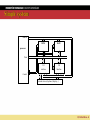
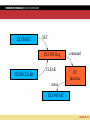
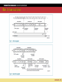
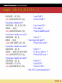
I/O interface -3
Simple system
Address
ROM
RAM
I/O
I/O
interface
Interface
processor
Data
Control
External devices (keyboard, display, ...)
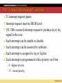
I/O interface -4
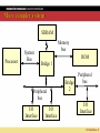
More complex system
SDRAM
Processor
System
Bus
Memory
bus
Bridge 1
Peripheral
bus
I/O
Interface
ROM
I/O
Interface
Bridge
2
Peripheral
bus
I/O
Interface
I/O interface -5
Example
An embedded system control an industrial process
On one side you have captor connected to input ports
On the other side you have motor unit connected to
output ports
The application do cycle made up of
Reading data from the input port (at a known memory
address)
Computing the data
Writing new data to the output port
I/O interface -6
Memory mapped register
Input / output port are device register that can be acceded in
the physical memory map
Memory mapped register
Memory mapped register, most of time, don't work like
standard memory use for variable
Read only (RO) or Write only (WO) registers
Variable size (8, 16, 32 bits)
Values can change outside the running application
The correct type must be used in C language
The 'volatile' term must be used (signals compiler that the
variable can be changed outside the program)
I/O interface -7
Samples
Using a simple pointer to access the I/O port
C macro
volatile unsigned *port = (unsigned int *) 0x40000000;
/*for an output port */ *port = value ;
/* for an input port */
variable = *port;
#define port *(volatile unsigned int *) 0x40000000
port = value ;
/* or value = port */
Using a macro provided by the kernel
HAL_WRITE_UINT32(address, value) or inl(int) or …
Using structure
struct port {
volatile unsigned config;
volatile unsigned data;
} *portA;
portA = (struct port *) 0x40000000;
portA->config = value1;
value2 = portA->data;
I/O interface -8
ARM7TDMI microprocessor
I/O interface -9
Presentation
32 bits general purpose architecture
3 stages pipeline RISC architecture
32 bits instructions (ARM mode) or 16 bits instructions
for code compression (THUMB mode)
Register to register and load/store architecture
Single bus for instruction and data
Low consumption (for embedded system)
I/O interface -10
Execution modes
7 execution modes
User (usr)
Supervisor (svc) privilieged for OS
FIQ (fiq) : Fast Interrupt
IRQ (irq) : Normal Interrupt
System (sys) privileged for OS
Abort (abt) addressing's fault
Undefined : not defined instruction
Changed are done by software or on special event (exceptions)
Modes out of usr are privileged modes
I/O interface -11
Registers
31 general purpose registers
Only 16 registers can be used in each mode
r0 → r15
In all mode
r15 is program counter (pc)
r14 is the link register (lr)
r13 is the stack pointer (sp)
By convention (AAPCS/EABI)
r4 to r11 are variable registers (v1 to v8)
r0 to r3 are scratch/argument registers (a1 to a4)
I/O interface -12
I/O interface -13
PSR
PSR : program state register
cpsr : current program state register
spsr : saved program state register (only present in privileged
mode)
CPSR contains
ALU flags (C,V, Z, N)
I and F flags for allowing interrupts
Processor mode
I/O interface -14
PSR
Mode
M[4:0]
User
10000
FIQ
10001
IRQ
10010
Supervisor
10011
Abort
10111
Undefined
11011
System
11111
I/O interface -15
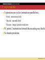
3 stages pipeline
3 operations per cycles (instructions parallelism)
Fetch : instructions fetch
Decode : operands fetch
Execute : integer operation and store
PC points 2 instructions forward the executing one (fetch)
No branch prediction
I/O interface -16
ARM instruction set
32 bits RISC instructions :
Register to register or register to immediate operand
operations
CPSR flags are not changed except if explicitly asked
Load/store instruction for moving data from register to/from
memory (register based addressing)
Most instructions can be conditionally executed
I/O interface -17
ARM instructions
I/O interface -18
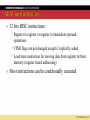
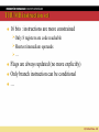
THUMB instruction set
16 bits : instructions are more constrained
Only 8 registers are code reachable
Shortest immediate operands
…
Flags are always updated (no more explicitly)
Only branch instruction can be conditional
…
I/O interface -19
THUMB instruction
I/O interface -20
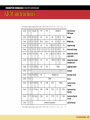
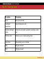
ARM7 exceptions
Exception
Description
Reset
Reset pin activated
Undefined
Instruction
Special instruction code
Software Interrupt
(SWI)
Instruction code used to generate exception, system
call
Prefetch Abort
Memory access violation during fetch
Data Abort
Data memory access violation
IRQ
IRQ pin activated
FIQ
FIQ pin activated
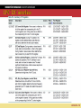
I/O interface -21
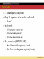
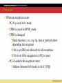
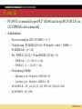
Principe
When an exception occurs
PC-4 is saved in lr_mode
CPSR is saved in SPSR_mode
CPSR is changed
Mode becomes : svc, irq, fiq, data or prefetch abort
depending the exception
I bit is set (IRQ not allowed) for all exceptions
F bit is set if the exception is a FIQ or reset
PC is loaded with exception vector
Address between 0x0 (reset) to 0x1C (FIQ)
I/O interface -22
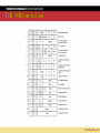
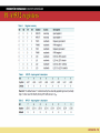
Exception vectors
address
Exception
Processor's mode
Priority
0x00
Reset
Supervisor (svc)
1
0x04
Undefined Instruction
Undef
6
0x08
Software Interrupt (SWI)
Supervisor (svc)
6
0x0C
Prefetch Abort
Abort
5
0x10
Data Abort
Abort
2
0x14
Reserved
0x18
IRQ (Interrupt)
irq
4
0x1C
FIQ (Fast Interrpt)
fiq
3
I/O interface -23
For arm processor each mode has their own stack pointer
Allow the exception handler to save data in its own memory area
without corrupting the application data
During the execution of the exception handler no interrupt are
allowed
No peripheral or system services can be serviced without
re-enable interrupt
Exception handler are architecture specific and differs from
standard function
Exception routine need special entry and exit code that can be
written in asm or provided by a library
I/O interface -24
Code example
; Exception Vectors
; Mapped to Address 0.
; Absolute addressing mode must be used.
; Dummy Handlers are implemented as infinite loops which can be modified.
Vectors
Reset_Addr
Undef_Addr
SWI_Addr
PAbt_Addr
DAbt_Addr
IRQ_Addr
FIQ_Addr
LDR
LDR
LDR
LDR
LDR
NOP
LDR
LDR
PC, Reset_Addr
PC, Undef_Addr
PC, SWI_Addr
PC, PAbt_Addr
PC, DAbt_Addr
; Reserved Vector
PC, IRQ_Addr
PC, FIQ_Addr
DCD
DCD
DCD
DCD
DCD
DCD
DCD
DCD
Reset_Handler
Undef_Handler
SWI_Handler
PAbt_Handler
DAbt_Handler
0
; Reserved Address
IRQ_Handler
FIQ_Handler
I/O interface -25
ARM architecture evolution
I/O interface -26
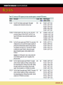
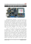
NXP - LPC2478
Nicolas Lacaille
LPC2478 -27
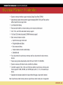
Présentation
Microcontroler from nxp with ARM7TDMI-S core
Running up to 80MHz
64 kbyte of SRAM
518 kbyte of flash program memory
External memory interface
An external memory controller is present to connect static or
dynamic RAM or FLASH
Peripherals
AHB peripherals (VIC, ethernet, usb, memory, FastGPIO)
APB peripherals (sérial, Timer, PWM, ADC, RT clock, ...)
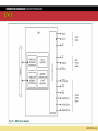
LPC2478 -28
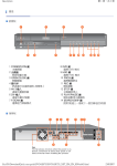
Block diagram
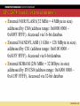
LPC2478 -29
Memory map
LPC2478 -30
Memory map
LPC2478 -31
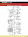
Remapping
ARM exception vectors are at address 0x0 → 0x1C
Remapping on LPC2478 consists in changing some
memory address to map vector address (64 byte from
0x0 to 0x3F)
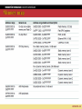
Modes :
LPC2478 -32
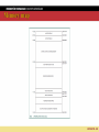
MEMMAP Register
LPC2478 -33
Flash bootloader
Provide initial operation after reset and means to
programs user flash memory
At reset, with certain conditions an ISP handler is
invoked (In System Programming)
P2.10 sampled low
Watchdog flag not set
If P2.10 is sampled High, the boot loader search for a
valid user program in flash
A checksum of exception vector is done (signature in 0x14
added with the sum of other exception vectors must be 0)
If checksum is valid the user program is launch otherwise no
LPC2478 -34
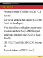
Clock
3 oscillators
Main oscillator : 1 to 24 MHz (12MHz)
Internal RC oscillator (4MHz)
RTC oscillator
All oscillator can drive a PLL and subsequently the CPU
PLL allow to choose the CPU clock frequency from the clock
source
f
pll =
2∗M
∗ f sected
N
LPC2478 -35
Clock
LPC2478 -36
Selecting clock
At startup, the internal RC oscillator is used and PLL is
bypassed
User boot can activate the main oscillator (SCS : system
Control ans Status Register)
When main oscillator is stabilized user program can use
it as clock source for the PLL (CLKSRCSEL register)
and activate it with specific value (PLLCFG to choose
M and N)
CPU (CCLKCFG) and USB (USBCLKCFG) divider are
set
Peripheral clocks are set (PCLKSEL0 and 1)
LPC2478 -37
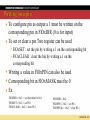
Example : ConfigurePLL() (framework.c)
void ConfigurePLL ( void ){
unsigned int MValue, NValue;
if ( PLLSTAT & (1 << 25) ){
PLLCON = 1;
PLLFEED = 0xaa;
PLLFEED = 0x55;
}
PLLCON = 0;
PLLFEED = 0xaa;
PLLFEED = 0x55;
/* Enable PLL, disconnected */
/* Disable PLL, disconnected */
SCS |= 0x20;
while( !(SCS & 0x40) );
CLKSRCSEL = 0x1;
/* Enable main OSC */
/* Wait until main OSC is usable */
/* select main OSC, 12MHz, as the PLL clock source */
PLLCFG = PLL_MValue | (PLL_NValue << 16);
PLLFEED = 0xaa;
PLLFEED = 0x55;
PLLCON = 1;
PLLFEED = 0xaa;
PLLFEED = 0x55;
CCLKCFG = CCLKDivValue;
#if USE_USB
USBCLKCFG = USBCLKDivValue;
#endif
/* Enable PLL, disconnected */
/* Set clock divider */
/* usbclk = 288 MHz/6 = 48 MHz */
while ( ((PLLSTAT & (1 << 26)) == 0) );
/* Check lock bit status */
MValue = PLLSTAT & 0x00007FFF;
NValue = (PLLSTAT & 0x00FF0000) >> 16;
while ((MValue != PLL_MValue) && ( NValue != PLL_NValue) );
PLLCON = 3;
/* enable and connect */
PLLFEED = 0xaa;
PLLFEED = 0x55;
while ( ((PLLSTAT & (1 << 25)) == 0) );
/* Check connect bit status */
}
LPC2478 -38
Peripheral clocks
PCLKSEL0
PCLKSEL1
LPC2478 -39
Power
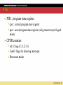
4 special modes of power reduction :
Idle
Clocks core stopped
Resume on reset or interrupt
Sleep
Main oscillator powered down and all clock stopped
Wake up on reset or interrupt
PLL must be reconfigured
Power-down
All clock powered down
Flash is powered down (unlike sleep)
Deep power-down
Power regulator turned off (register values are not retained)
LPC2478 -40
Peripheral power control
Each peripheral can be turned off (clock disable)
Control of power peripheral done through PCONP reg.
1 : enable
0 : disable
If peripheral is disable, read or write register are not valid
LPC2478 -41
Peripheral power control
Each peripheral can be turned off (clock disable)
Control of power peripheral done through PCONP reg.
1 : enable
0 : disable
If peripheral is disable, read or write register are not valid
LPC2478 -42
External Memory Controller
LPC2478 -43
EMC
LPC2478 -44
LPC2478 board : external memory
External NOR FLASH (32 MBit = 4 MByte in size)
addressed by CS0 (address range: 0x8000 0000 –
0x80FF FFFF). Accessed via 16-bit databus.
External NAND FLASH (1 GBit = 128 MByte in size)
addressed by CS1 (address range: 0x8100 0000 –
0x81FF FFFF). Accessed via 8-bit databus.
External SDRAM (256 MBit = 32 MByte in size)
addressed by DYCS0 (address range: 0xA000 0000 –
0xA1FF FFFF). Accessed via 32-bit databus
LPC2478 -45
Memory Accelerator Module
Small SRAM memory between flash and core
Allow fast instruction access
Direct access to flash is limited to 20MHz (50ns access time)
Load 4 arm instructions from flash
2 buffers are alternatively used to maintain prefetch rate
Include a branch trail buffer for loops
/* Set memory accelerater module*/
MAMCR = 0;
#if Fcclk < 20000000
MAMTIM = 1;
#else
#if Fcclk < 40000000
MAMTIM = 2;
#else
MAMTIM = 3;
#endif
#endif
MAMCR = MAM_SETTING;
//0=disabled, 1=partly enabled (enabled for code prefetch, but not for data), 2=fully enabled
LPC2478 -46
PIN
To reduce number of pins on chip, pins are multiplexed
Different functions can use the pins
Registers which are controlling pin function are
PINSEL (PINSEL0 to PINSEL11)
PINMODE (PINMODE0 to PINMODE9)
PINSEL controls
pin multiplexer
PINMODE define
electrical pin connexion
LPC2478 -47
Exemple
GPIO port 0.1
00
CAN1 :TD1
01
P0.1
UART3 : RXD3
10
Chip's pin
I2C1 SCL1
11
CHIP
LPC2478 -48
GPIO : General Purpose I/O
5 general purpose 32 bits port
GPIO controller are located on the local bus for fast
controlling
Port0 and Port1 can also be controlled by legacy control
register on APB bus (slow)
Port0 and Port2 can generate interrupts on individual
change of individual pin
Each individual pin can be configured as input or out put
(FIOxDIR)
Each individual pin can be masked (FIOxMASK) for
reading and writing (read 0 and no effects on write)
LPC2478 -49
Registers
LPC2478 -50
Writing on a pin
To configure pin as output a 1 must be written on the
corresponding pin in FIOxDIR (0 is for input)
To set or clear a pin Two register can be used
FIOxSET : set the pin by writing a 1 on the corresponding bit
FIOxCLEAR : clear the bin by writing a 1 on the
corresponding bit
Writing a value in FIOxPIN can also be used
Corresponding bit in FIOxMASK must be 0
Ex
FIO0DIR = 0x2 ; // set direction for bit 1
FIO0SET = 0x2; // set P0.1
FIO0CLEAR = 0x2; // clear P0.1
FIO0DIR = 0x2 ;
FIO0PIN |= 0x2; // set P0.1
FIO0PIN &= ~0x2; // clear P0.1
LPC2478 -51
Interrupt with GPIO
Port0 and 2 can be configured to generate interrupt
2 pairs of enable/status registers are present : one for a
rising edge and one for falling edge
InEnF/R : enable corresponding pin for interrupt
IntStatF/R (RO) : to verify which pin has generate interrupt
Interrupt must be cleared through IntClr register
LPC2478 -52
Exemple
void led210_init(void){
// Power control
//GPIO cannot be turned off
// CLOCK
PCLKSEL1 &= ~(0x3 << 2); //3:2 = 0b00 (CCLK / 4)
// PIN :
// function select for P2.10 (GPIO) in PINSEL4 (PINSEL4[21..20] = 0b00) (RW)
PINSEL4 &= ~(3 << 20) ;
// connect mode selection for pin (00 = pull up resistor selected) (RW)
PINMODE4 &= ~(3 << 20) ;
//PIO
// direction mode selection : output = 1 et input = 0 (out selected) (R/W)
FIO2DIR |= (1 <<10);
// to allowed read an write on the selected pin (0 = enable)
FIO2MASK &= ~(1 <<10);
}
void led210_turn_on(void){
FIO2CLR = 1<<10;
}
void led210_turn_off(void){
FIO2SET = 1<< 10;
}
LPC2478 -53
Clock for pio :chap4 p59 & 60
PCLKSEL1 &= ~(0x3 << 2);
The 2 bits 3:2 are cleared,
selecting a clock of CCLK/4 for
the GPIO
LPC2478 -54
PINconnect
/* function select for P2.10 (GPIO) in PINSEL4
(PINSEL4[21..20] = 0b00 ) (RW) */
PINSEL4 &= ~(3 << 20) ;
LPC2478 -55
General purpose timer
The LPC2478 includes four 32-bit Timer/Counters
Count cycles of the system derived clock or an externally-supplied
clock
Include programmable 32-bit prescaler
Can optionally generate interrupts or perform other actions at
specified timer values, based on four match registers
Set LOW on match, Set HIGH on match, Toggle on match, Do nothing on
match.
The Timer/Counter also includes four capture inputs to trap the
timer value when an input signal transitions
A capture event may also optionally generate an interrupt
LPC2478 -56
Prescaler
LPC2478 -57
Prescaler and Timer counter control
Prescaler :
Each PCLK edge the prescaler counter is incremented
When the prescaler counter equals the prescaler register the
timer counter is incremented and the prescaler counter is
cleared
Timer Control register :
Enable or disable the 2 counter (prescaler and timer)
reset of the timer counter and the prescaler counter
LPC2478 -58
Capture mode
Use to measure pulse duration
Counter captured on external events on CAP pin
Rising edge, falling edge, toggle
Interrupt request can be generated by a capture
LPC2478 -59
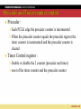
Match mode
Used to control the counter
Disable or reset the counters
Can generate an interrupt request on match
The pin level can be changed on match (external match register)
Set, cleared, toggle
LPC2478 -60
Timing on match
LPC2478 -61
User manual
LPC2478 -62
Lab Example
static void mdelay(unsigned int ms)
{
T1TCR = 0x02;
// stop and reset timer
T1PR = 0x00;
// set prescaler to zero
T1MR0 = ms * (Fpclk / 1000); // Fpclk = 36000000
T1MCR = 0x04;
// stop timer on match
T1TCR = 0x01;
// start timer
//wait until delay time has elapsed : test the 'enable' bit
while(T1TCR & 0x01)
;
}
LPC2478 -63
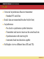
I2C
Inter Integrated Circuit (Two Wire Interface)
Two wire communication bus (synchronous serial
transmission)
Multimaster
400kbit/s (for slow devices)
Each device has an address (8 or 10 bits) which is used
when addressed in slave mode
LPC2478 -64
I2C bus connection
LPC2478 -65
Transfer
Master drives the clocks and initiate transfer
Slave respond to master request
A Transmission is started by a “start” sequence
Data are transferred in sequence of 8 bits (from/to
master) MSb first
Data are changed during low edge of clock
Data must be stable during high edge of clock
Transmission ends with a “stop” sequence
For each 8 bits data receiver must acknowledge sender
by sending an “ack” bit (low level)
LPC2478 -66
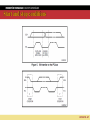
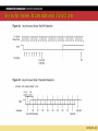
Start and stop conditions
LPC2478 -67
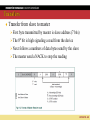
Transfers
Transfer from master to slave
First byte transmitted by master is slave address (7 bits)
The 8th bit is low signaling a write to the device
Next follows a numbers of data bytes
Slave returns an ACK bit after each received byte
LPC2478 -68
Transfers
Transfer from slave to master
First byte transmitted by master is slave address (7 bits)
The 8th bit is high signaling a read from the device
Next follows a numbers of data bytes send by the slave
The master send a NACK to stop the reading
LPC2478 -69
LPC I2C interface
LPC2478 -70
I2CONSET
SET
I2CONT Reg
I2CONCLEAR
CLEAR
command
I2C
Interface
status
I2CONSTAT
LPC2478 -71
Handling the interface
Master Transmitter mode
Initialize ICONSET (clear SI/STA/STO in I2CONCLR)
Set the STA bit (SI bit is set when done and a new status code
is present in I2STAT)
Place data in I2DAT register (Address for first byte)
Clear SI and STA
Wait for SI (set when data has been sent, new status code)
Place new data
…
Set STO to end transmission
LPC2478 -72
Sample code
I20CONSET = I2C_STA;
while (!(I20CONSET & I2C_SI));
/* check status to handle error */
I20CONCLR = I2C_SI | I2C_STA;
/* send START */
/* Wait for START */
I20DAT = slave_address;
while (!(I20CONSET & I2C_SI));
/* check status to handle error (nack)*/
I20CONCLR = I2C_SI;
/* slave address */
/* Wait for ADDRESS send */
I20DAT = data0;
while (!(I20CONSET & I2C_SI));
/* check status to handle error (nack)*/
I20CONCLR = I2C_SI;
/* data 0*/
/* Wait for DATA send */
I20CONSET = I2C_STO;
while (I20CONSET & I2C_STO);
/* clear SI and STA */
/* clear SI */
/* clear SI */
/* send STOP */
/* Wait for STOP */
/* note : STO is cleared automatically */
LPC2478 -73
Note
Controlling interface
For every events
SI is set
A status code is present in I2STAT
When SI is set, the status code can be used to take appropriate
action
After each operation, software must wait for SI to be set
(interruption can be used)
Bit AA is used to allow interface to become slave
Repeated STA (new start before stop) must be used with
some interface (selecting register inside a device before
a read by example)
LPC2478 -74
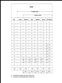
Status code
LPC2478 -75
Sample 2 : using I2CISR
Void I2CISR(void) {
switch(I2STAT){
case (0x08) :
I2CONCLR = I2C_STA;
I2DAT = I2CAddress;
break;
case(0x18):
I2DAT = I2CData;
break;
case(0x20):
I2DAT = I2CAddress;
break;
case(0x28):
I2CONSET = I2C_STO;
break
default :
break;
}
I2CONCLR = I2C_SI;
VICVectAddr = 0;
}
//start bit
//send address
//slave address ack
// slave address nack
// data ack
// clear interrupt flag
//VIC ack
LPC2478 -76
Exemple of device : PC19532 (led driver)
I2C 16 led driver
Controlled by 10 registers
Writing
Sending address of the device : 0xC0
Sending the number of the register
Sending data to the device register
Reading
Sending address of the device : 0xC0
Sending the number of the register
Sending address of the device : 0xC1 with repeated STA
read data from the device register
LPC2478 -77
Bus transaction
LPC2478 -78
PCA9532 registers
LPC2478 -79
PCA9532 registers
LPC2478 -80
Example
PCA9532 is connected to pin P0.27 (SDA0) and to pin P0.28 (SCL0) (an
I2C EPROM is also connected)
Initialization
Power activation for I2C0 : PCONP0 |= 1 <<7
Clock division : PCLKSEL0[15:14] = 00 for pclk = cclk/4 = 18MHz =>
PCLKSEL0 &= ~(3<<14)
Pin : PINSEL1 [23:22] = 01 and PINSEL1 [25:24] = 01
PINSEL &= ~( (3 <<22) | (3 << 24))
PINSEL1 |= (1 << 22) | (01 << 24)
Clock timing (100kHz)
High duty cycle = 90 pclk tic : I20SCLH = 90
Low duty cycle = 90 pclk tic : I20SCLL = 90
I2C0CONCLR = I2C_AA | I2C_SI | I2C_STO | I2C_STA | I2C_I2EN
I2C0CONSET = I2C_I2EN
LPC2478 -81
Sample code to light led 8 to 11
I20CONSET = I2C_STA;
/* send START */
while (!(I20CONSET & I2C_SI));
/* Wait for START */
/* check status to handle error */
I20CONCLR = I2C_SI | I2C_STA;
/* clear SI and STA */
I20DAT = 0xC0;
/* PCA address */
while (!(I20CONSET & I2C_SI));
/* Wait for ADDRESS send */
/* check status to handle error (nack)*/
I20CONCLR = I2C_SI;
/* clear SI */
I20DAT = 0x18;
/* select register LS2 and AI*/
while (!(I20CONSET & I2C_SI));
/* Wait for DATA send */
/* check status to handle error (nack)*/
I20CONCLR = I2C_SI;
/* clear SI */
I20DAT = 0x01 | 0x4 | 0x10 | 0x40 ;
/* 4 leds on : led8 to 11 */
while (!(I20CONSET & I2C_SI));
/* Wait for DATA send */
/* check status to handle error (nack)*/
I20CONCLR = I2C_SI;
/* clear SI */
I20CONSET = I2C_STO;
/* send STOP */
while (I20CONSET & I2C_STO);
/* Wait for STOP */
/* note : STO is cleared automatically */
LPC2478 -82
VIC : Vectored Interrupt Controller
32 interrupt request inputs
Interrupt request must be HIGH level
VIC ORs vectored interrupt request to produce irq or fiq
signal to the core
Each interrupt can be enable or disable
Each interrupt can be asserted by software
Each interrupt is assigned to irq or fiq line
Each interrupt is programmed with a priority on 4 bits
0 : highest priority
15 : lowest priority
LPC2478 -83
Diagram
LPC2478 -84
VIC registers
...
LPC2478 -85
Registers
VICSoftInt : ORed with interrupt request
VICSoftIntClear : to clear one or more bit in VICSoftInt
VICIntEnable : enable soft and hard irq
VICIntEnClear : to clear one or more bit in VICIntEnable
VICProtect : allow usr mode to access VIC register
VICIntSelect : contribue to irq(0) or fiq (1)
VICIrqStatus/VICFiqStatus : show active irq/fiq request
VICVectAddr0-31 : isr address for each request lines
VICVectPriority0-31 : priority for each request lines, 0 to 15 with 15
lowest priority
VICAddress : address of isr that is to be serviced
Musts be written at end of isr to acknowledge the IRQ
LPC2478 -86
Interrupt flow
When interrupt N occurs, if interrupt is enable the irq
line is asserted
If the interrupt line is not masked
Bit N in VICIntEnable set
The current priority is lower than the priority assigned to the
corresponding IRQ N
The VICVectAddrN of associated interrupt is copied in
VICAddress register to be read by software (most of
time this is the isr address)
The IRQ (or FIQ) line connected to the core is asserted
...
LPC2478 -87
When software read VICAddress :
the irq (fiq) line to the core is de-asserted
Hardware priority in VIC is set to the highest priority irq pending (here N)
During the time of the irq is serviced by software
If an irq M with lower priority appears : nothing occurs
If an irq M with higher priority appears : same stages as described before
(activation of the irq line, copy of VICVectAddrM, ...)
When interrupt is serviced, software must write a dummy value in
VICAddress
This signal the end of the treatment and the Hardware priority in VIC is
lowered to the higher pending irq priority
LPC2478 -88
Interrupt lines
LPC2478 -89
Example of vectored irq usage
For vectorized irq, each interrupt routine address (isrx)
must be written in VICVectAddrx
At irq vector address (0x18) instruction load pc with
VIC address and so jump to the appropriate isr :
Vectors
LDR PC, Reset_Addr
LDR PC, Undef_Addr
LDR PC, SWI_Addr
LDR PC, PAbt_Addr
LDR PC, DAbt_Addr
NOP
; Reserved Vector
LDR PC, [PC, #-0x0120] ; Vector from VicVectAddr
LDR PC, FIQ_Addr
LPC2478 -90
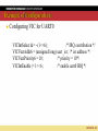
Exemple of configuration
Configuring VIC for UART0
VICIntSelect &= ~(1<<6) ;
/* IRQ contribution */
VICVectAddr6 = (unsigned long) uart_isr ; /* isr address */
VICVectPriority6 = 10;
/* priority = 10*/
VICIntEnable |= 1<<6 ;
/* enable uart0 IRQ */
LPC2478 -91
Vectored interrupt flow
1. An interrupt occurs.
2. The ARM processor branches to either the IRQ or FIQ interrupt vector.
3. If the interrupt is an IRQ, read the VICVectAddr Register and branch to the interrupt
service routine. You can do this using an LDR PC instruction. Reading the VICAddress
Register updates the interrupt controllers hardware priority register.
4. Stack any registers that will be used to avoid any register corruption
5. Execute the service
6. Clear the requesting interrupt in the peripheral, or write to the VICSoftIntClear
register if the request was generated by a software interrupt.
7. Restore the previously saved register
8. Write to the VICAddress Register. This clears the respective interrupt in the internal
interrupt priority hardware.
9. Return from the interrupt. This re-enables the interrupts.
LPC2478 -92
Vectored interrupt example code
0x18
LDR pc, [pc, #-0x120]
@ Load Vector into PC
@ .......................................................
vector_handler
@Code to enable interrupt nesting
STMFD r13!, {r0-r3, r12, lr} @ stack registers that will be corrupted by a function call
@ Interrupt service routine...
BL 2nd_level_handler
@ this corrupts lr_irq and r0-r3 and r12
@...
@Add code to clear the interrupt source;
@Code to exit handler
LDMFD r13!, {r0-r3, r12, r14}
@ unstack lr_irq and r0-r3, r12
LDR r1, =VectorAddr
STR r0, [r1]
@ Acknowledge VIRQ serviced with a dummy write
SUBS pc, lr, #4
@ Return from ISR
LPC2478 -93
Vectored interrupt flow with nested interrupts
1. An interrupt occurs.
2. The ARM processor branches to either the IRQ or FIQ interrupt vector.
3. If the interrupt is an IRQ, read the VICVectAddr Register and branch to the interrupt
service routine. You can do this using an LDR PC instruction. Reading the VICAddress
Register updates the interrupt controllers hardware priority register.
4. Stack the workspace so that you can re-enable IRQ interrupts.
5. Enable the IRQ interrupts so that a higher priority can be serviced.
6. Execute the Interrupt Service Routine (ISR).
7. Disable the interrupts and restore the workspace.
8. Clear the requesting interrupt in the peripheral, or write to the VICSoftIntClear
register if the request was generated by a software interrupt.
9. Write to the VICAddress Register. This clears the respective interrupt in the internal
interrupt priority hardware.
10. Return from the interrupt. This re-enables the interrupts.
LPC2478 -94
Vectored interrupt example code
0x18
LDR pc, [pc, #-0x120]
@ Load Vector into PC
@ .......................................................
vector_handler
@ Code to enable interrupt nesting
STMFD r13!, {r12, r14} @stack lr_irq and r12 [plus other regs used below, if appropriate]
MRS r12, spsr
@ Copy spsr into r12...
STMFD r13!, {r12}
@ and save to stack
MSR cpsr_c, #0x1f
@ Switch to SYS mode, re-enable IRQ
STMFD r13!, {r0-r3, r14}
@stack lr_sys and r0-r3
@ Interrupt service routine...
@Add code to clear the interrupt source; Code to exit handler
BL 2nd_level_handler
@ this corrupts lr_sys and r0-r3
LDMFD r13!, {r0-r3, r14}
@ unstack lr_sys and r0-r3
MSR cpsr_c, #0x92
@ Disable IRQ, and return to IRQ mode
LDMFD r13!, {r12} @ unstack r12...
MSR spsr_cxsf, r12
@ and restore spsr...
LDMFD r13!, {r12, r14}
@ unstack registers
LDR r1, =VectorAddr
STR r0, [r1]
@ Acknowledge VIRQ serviced
SUBS pc, lr, #4
@ Return from ISR
LPC2478 -95
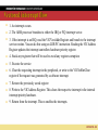
Interrupt using a library (to avoid asm)
Some toolchains can provide entry/exit code of a
interrupt routine
Basic entry/exit code
To use more complex code (to allow nested interrupt or to
switch context, ... ) you still have to write the entry/exit code
in asm
With gcc you can use the “attribute” keyword to modify
the entry/exit code of a function.
For a interrupt use “interrupt” attribute :
void myISR(void) __attribute__ ((interrupt));
Pour ARM : __attribute__ ((interrupt ("IRQ")));
LPC2478 -96
UART
Universal Asynchronous Receiver/transmitter
Standard PC serial line
Serial :data are transmitted bit after bit (lsb first)
Asynchronous
No clock to synchronize symbol detection
Transmitter and receiver must use the same baud rate
Synchronization with start/stop bit
Automatic baud rate detection capable
Full duplex via two different lines (RX and TX)
LPC2478 -97
Asynchronous transmission detection
LPC2478 -98
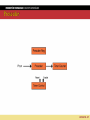
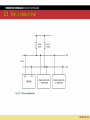
Diagram of a serial interface
UnTHR
Application
Application
FIFO
serializer
TX
serializer
RX
Lines
FIFO
UnRBR
LPC2478 -99
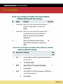
LPC2478 UART0/1/2/3 register overview
16 bytes FIFO for receiver and transmitter
Write and read from a unique register : Read Buffer Register
(UnRBR) and Transmit Holding Register (UnTHR)
Trigger point 1, 4, 8, 14 for receiver
Line Status Register (UnLSR) for status information
Data received or transmitted, error on received data, ...
Control
UARTn Line Control Register (UnLCR) : Number of bits, stop
bit, parity enable , parity type, divisor latch access(DLAB)
FIFO Control Register (UnFCR) to reset emitter or transmitter
and to chose receiver's fifo trigger
LPC2478 -100
LPC2478 UART0/1/2/3 register overview
Baud rate
Divisor latch (UnDLL and UnDLM)
Fractional Divider Register (UnFDR) for baud rate
Interrupt
Interrupt Enable Register (UnIER) to allow interrupt source
request to the system (data received, transmitter's fifo empty,
received data error or time-out)
Interrupt Identification Register (UnIIR) to identify the
interrupt source
LPC2478 -101
UART registers
LPC2478 -102
UART registers
LPC2478 -103
Baud rate
To allow a working serial line the baud rate must be set
to match both emitter/transmitter device
The baud rate is selected with 2 registers
UnDLM an UnDLL which are respectively at UnTHR and
UnRBR address location when DLAB in UnLCR is set
Fractional Divider Register (UnFDR)
LPC2478 -104
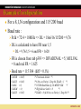
Example of configuration
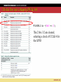
For a 8,1,N configuration and 115 200 baud
Baud rate :
Pclk = 72/4 = 18MHz => DL = 18e6/16/115200 = 9,76
DL is calculated to have FR near 1,5
DL = 9,76/1,5 = 6 and FR = 1.628
FR is chosen from tab p393 => DIVADDVAL = 5; MULVAL
= 8 and real FR = 1.625
Baud rate = 115 384 (diff = 0,1%)
UnFDR
UnLCR
UnDLL
UnDLM
UnLCR
= 0x85;
= 0x83;
= 6;
= 0;
= 0x03;
/* Fractional divider */
/* 8 bits, no Parity, 1 Stop bit DLAB = 1 */
/* 115200 Baud Rate @ 18 MHZ PCLK
*/
/* High divisor latch = 0
*/
/* DLAB = 0 (& 8 bits, no Parity, 1 Stop bit) */
LPC2478 -105
UART Status register UnLSR
LPC2478 -106
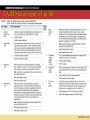
Using UART
Configure the baud rate
Configure bit number, parity, stop bit, ...
Optionally reset emitter and transmitter and enable fifo
Transmitting data
Write in UnTHR (up to 16 byte)
Wait for THE (transmitter's fifo empty) flag to set or for
Transmitter empty (TEMT) flag signaling serializer empty
(last byte completely transfered)
Write other data in UnTHR
....
THE can be source of IRQ
LPC2478 -107
Using UART
Receiving data
RDR in UnLSR is set when an unread data is present in the
RBR FIFO
Software waiting for data must poll RDR bit (wait for RDR to
be set)
Software must read data from UnRBR until RDR is cleared
Using interrupt
UnIER allow interrupt request on THRE, RBR, RX line status
(Overrun error (OE), Parity Error (PE), break (BI)) and time
out on reception
UnIIR allow software to identify interrupt source
LPC2478 -108
Simple receiving/transmitting (polling)
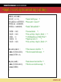
void init_serial (void) {
PCONP |= (1 <<3);
/* Enable UART0 power */
PCLKSEL0 &= 0xFFFFFF3F; /*Pclock uart0 = Cclock/4 */
PINSEL0 &= ~0x000000F0;
PINSEL0 |= 0x00000050;
/* Enable TxD0 and RxD0 */
U0FDR
U0LCR
U0DLL
U0DLM
U0LCR
= 0x85;
= 0x83;
= 6;
= 0;
= 0x03;
/* Fractional divider
*/
/* 8 bits, no Parity, 1 Stop bit , DLAB = 1 */
/* 115200 Baud Rate @ 18 MHZ PCLK */
/* High divisor latch = 0
*/
/* 8 bits, no Parity, 1 Stop bit , DLAB = 0 */
}
int sendchar (int ch) {
while (!(U2LSR & 0x20));
return (U2THR = ch);
}
/* Write character to Serial Port */
/* Wait for transmitt buffer empty */
int getkey (void) {
while (!(U2LSR & 0x01));
return (U2RBR);
}
/* Read character from Serial Port */
/* Wait for receive buffer not empty */
LPC2478 -109
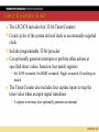
Real time clock
The RTC is a set of counters for measuring time when
system power is on, and optionally when it is off
RTC can be clocked by a separate 32.768 kHz oscillator
or by a programmable prescaler divider based on PCLK
RTC and battery SRAM have a separate power domain
supplying 3.3V to the Vbat pin
Provides Seconds, Minutes, Hours, Day of Month,
Month, Year, Day of Week, and Day of Year.
LPC2478 -110
RTC Interrupt
An alarm output pin is included to assist in waking up
when the chip has had power removed to all functions
except the RTC and Battery RAM.
Periodic interrupts can be generated from increments of
any field of the time registers, and selected fractional
second values.
This enhancement enables the RTC to be used as a System
Timer.
The alarm registers allow the user to specify a date and
time for an interrupt to be generated
LPC2478 -111
RTC Interrupt
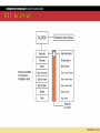
LPC2478 -112
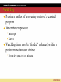
Watchdog
Provide a method of recovering control of a crashed
program
Timer that can produce
Interrupt
Reset
Watchdog timer must be “feeded” (reloaded) within a
predetermined amount of time
From few μsec to few minutes
LPC2478 -113
Other Interface
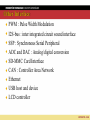
PWM : Pulse Width Modulation
I2S-bus : inter integrated circuit sound interface
SSP : Synchronous Serial Peripheral
ADC and DAC : Analog/digital conversion
SD-MMC Card Interface
CAN : Controller Area Network
Ethernet
USB host and device
LCD controller
LPC2478 -114
LPC2478 -115