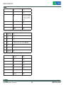
1
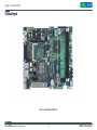
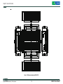
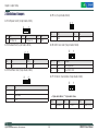
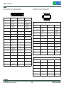
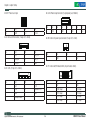
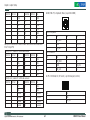
Building the Digital Infrastructure
NISE 3110 User Manual
Version 1.6
February, 2009
Preface
Copyright Notice
FCC Class A
Copyright © 2006 NEXCOM
All rights reserved. No part of this manual may be reproduced, transmitted, transcribed, stored in a retrieval system, or translated into any language or computer
language, in any form or by any means (electronic, mechanical, photocopying,
recording, or otherwise), without the express written permission of NEXCOM
Information provided in this manual is intended to be accurate and reliable.
However, the original manufacturer assumes no responsibility for its use, nor for
any infringements upon the rights of third parties that may result from such use.
This equipment has been tested and found to comply with the limits for a Class A
digital device, pursuant to part 15 of the FCC Rules. These limits are designed to
provide reasonable protection against harmful interference when the equipment
is operated in a commercial environment.
This equipment generates, uses, and can radiate radio frequency energy and,
if not installed and used in accordance with the instruction manual, may cause
harmful interference to radio communications. Operation of this equipment in a
residential area is likely to cause harmful interference in which case the user will
be required to correct the interference at his own expense.
Acknowledgements
Installation Suggestions
Intel and Pentium are trademarks of Intel Corporation.
Microsoft Windows® is a registered trademark of Microsoft Corp.
All other product names or trademarks are properties of their respective owners.
Ensure you have a stable, clean working environment. Dust and dirt can get into
components and cause a malfunction. Use containers to keep small components
separated.
Adequate lighting and proper tools can prevent you from accidentally damaging
the internal components. Most of the procedures thatfollow require only a few
simple tools, including the following:
A Philips screwdriver
A flat-tipped screwdriver
A grounding strap
An anti-static pad
Using your fingers can disconnect most of the connections. It is
recommended that you do not use needlenose pliers to disconnect connections
as these can damage the soft metal or plastic parts of the connectors.
Declaration of Conformity
CE
This product has passed the CE test for environmental specifications when
shielded cables are used for external wiring. We recommend the use of shielded
cables. Please contact your local supplier for ordering information.
This product has passed the CE test for environmental specifications. Test conditions for passing included the equipment being operated within an industrial
enclosure. In order to protect the product from being damaged by ESD (Electrostatic Discharge) and EMI leakage, we strongly recommend the use of CE-compliant industrial enclosure products.
Copyright © 2006 NEXCOM International Co., LTD. All rights reserved
2
NISE3110 User Manual
Preface
Handling Precautions
?? Always disconnect the unit from the power outlet whenever you are installing
or fixing a component inside the chassis.
?? If possible, always wear a grounded wrist strap when you are installing or
fixing a component inside the chassis. Alternatively, discharge any static electricity by touching the bare metal chassis of the unit case, or the bare metal
body of any other grounded appliance.
?? Hold electronic circuit boards by the edges only. Do not touch the components on the board unless it is necessary to do so. Do not flex or stress the
circuit board.
?? Use the correct screws and do not overly tighten them.
?? Keep the original packaging and static-protective bag in case the unit has to
be returned.
Copyright © 2006 NEXCOM International Co., LTD. All rights reserved
3
NISE3110 User Manual
Warranty and RMA
NEXCOM RMA Policy
?? 2.5 Any products returned by NEXCOM to other locations besides the customers’ site will bear an extra charge and will be billed to the customer.
1.Warranty Period
3. Repair service charges for out of warranty products
NEXCOM manufactures products that are new or equivalent to new in accordance
with industry standard. NEXCOM warrants that products will be free from defect
in material and workmanship for 24 months beginning on the date of invoice
by NEXCOM. HCP series products (Blade Server) which are manufactured by
NEXCOM are covered by a three year warranty period.
NEXCOM will charge for out of warranty products in two categories, one is basic
diagnostic fee and another is component (product) fee.
System level
?? Component fee: NEXCOM will only charge for main components, such as
SMD chip, BGA chip, etc. Passive components will be repaired for free, ex:
resistor, capacitor.
2. RMA (Return Merchandise Authorization)
?? Customers shall enclose the “NEXCOM RMA Service Form” with the returned
packages.
?? Items will be replaced with NEXCOM products if the original one is not able to
be repaired. Ex: motherboard, power supply, etc.
?? Customers must collect all the information about the problems encountered
and note anything abnormal or, print out any on-screen messages, and
describe the problems on the “NEXCOM RMA Service Form” for the RMA
number apply process.
?? Replaced with 3rd party products if needed.
?? If RMA goods can not be repaired, NEXCOM will return it to customer without
any charge.
?? Customers can send back the faulty products with or, without accessories
(manuals,cable, etc.) and any unnecessary components from the card, such
as CPU and RAM.
If the components were suspected as part of the problems, please note clearly
that which components are included. Otherwise, NEXCOM is not responsible
for the devices/parts.
Board level
?? Component fee: NEXCOM will only charge for main components, such as
SMD chip, BGA chip, etc. Passive components will be repaired for free, ex:
resistors, capacitors.
?? If RMA goods can not be repaired, NEXCOM will return it to customer without
any charge.
?? Customers are responsible to for the safe packaging of defective products are
durable enough to be resistant against further damage and deterioration during transportation. In case of damages occurred during the transportation, the
repair is treated as “Out of Warranty.”
Copyright © 2006 NEXCOM International Co., LTD. All rights reserved
4
NISE3110 User Manual
Warranty and RMA
Global Service Contact Information
NEXCOM Japan
10F, Nakagin-Shiroyama Building,
8-16-13 Ginza Chuou-Ku,
Tokyo, Japan 104-0061
Tel: 81-3-3524-4250
Fax: 81-3-3524-4252
Email: [email protected]
Website: www.nexcom-jp.com
Headquarters
NEXCOM International Co. Ltd.
18F, No.716, Chung-Cheng Road Chung-Ho City,
Taipei County 235, Taiwan, R.O.C.
Tel: 886-2-8228-0606
Fax: 886-2-8228-0501
Email: [email protected]
Website: www.nexcom com.tw
China
NEXCOM China
Room 301, Block E, Power Creative Building,
No.1 Shangdi East Rd.
Haidian District Beijing, 10085, China
Tel: 86-10-5885-6655
Fax: 86-10-5885-1006
Email: [email protected]
Website: www.nexcom.cn
USA
NEXCOM USA
3758, Spinnaker Court, Fremont, CA 94538, US A.
Tel: 1-510-656-2248
Fax: 1-510-656-2158
Email: sales@nexcom com
Website: www.nexcom.com
Europe
NEXCOM UK
10 Vincent Avenue, Crownhill
Milton Keynew, Buckinghamshire
MK8 0AB, United Kingdom
Tel: 44-(0)-1908-21 88 77
Fax: 44-(0)-1908-21 88 67
Email: [email protected]
Website: www.nexcomuk.co.uk
Japan
Copyright © 2006 NEXCOM International Co., LTD. All rights reserved
5
NISE3110 User Manual
Warranty and RMA
RoHS Compliance
How do you recognize NEXCOM RoHS Products?
For existing products where there are non-RoHS and RoHS versions, the suffix
“(LF)” will be added to the compliant product name.
For example, PEAK 7220VL2G RoHS version will become PEAK 7220VL2G(LF).
All new product models launched after January 2006 will be RoHS compliant.
They will use the usual NEXCOM naming convention.
For example, PEAK 870VL2, NBP14570, EBC 420 etc. All RoHS compliant
model and component manufacturing part numbers will be suffixed “X00”
NEXCOM RoHS Environmental Policy and Status Update.
Nexcom is a global citizen for building the digital infrastructure. We are committed to providing green products and
services, which are compliant with European Union RoHS
(Restriction on Use of Hazardous Substance in Electronic
Equipment) directive 2002/95/EU, to be your trusted green partner and to protect
our environment.
RoHS restricts the use of Lead (Pb) < 0.1% or 1,000ppm, Mercury (Hg) < 0.1%
or 1,000ppm, Cadmium (Cd) < 0.01% or 100ppm, Hexavalent Chromium (Cr6+)
< 0.1% or 1,000ppm, Polybrominated biphenyls (PBB) < 0.1% or 1,000ppm,
and Polybrominated diphenyl Ethers (PBDE) < 0.1% or 1,000ppm.
In order to meet the RoHS compliant directives, NEXCOM has established an
engineering and manufacturing task force in to implement the introduction of
green products. The task force will ensure that we follow the standard NEXCOM
development procedure and that all the new RoHS components and new
manufacturing processes maintain the highest industry quality levels for which
NEXCOM are renowned.
The model selection criteria will be based on market demand. Vendors and
suppliers will ensure that all designed components will be RoHS compliant.
Copyright © 2006 NEXCOM International Co., LTD. All rights reserved
Manual Revision History
6
Revision
Date
Description
1.0
Sep., 07
First Edition, V1.0
1.1
Nov. 07
Add Appendix C “power consumption”
1.2
Feb.,08
Correct P28 GPIO pin definition (J11)
1.3
March, 08 Add the Appendix E: Display Setting
Modify the Appendix B: GPIO Programming guide
(add the note for SPC150)
1.4
July.,08
Add Appendix F: “IEGD installation guide“ to resolve
no display issue
1.5
Jan.,09
Add Appendix G: Award BIOS Setup
1.6
Feb. 09
Add DB44 to DB9 COM cable connector pin definition
NISE3110 User Manual
Warranty and RMA
Copyright © 2006 NEXCOM International Co., LTD. All rights reserved
7
NISE3110 User Manual
Table of Content
Table of Content
?? 1.6 Board Layout........................................................................................... 14
?? Copyright Notice............................................................................................. 2
Figure 1.2 Top View ofr the EBC 576............................................................. 14
?? Acknowledgements. ........................................................................................ 2
?? 1.7 Dimension Drawing ................................................................................ 15
?? Declaration of Conformity. .............................................................................. 2
Figure 1.3: Dimension drawing of EBC 576 . ................................................ 15
?? Installation Suggestions.................................................................................. 2
Figure 1.4 Dimension drawing of NISE 3110 . .............................................. 16
?? Handling Precautions...................................................................................... 3
Chapter 2 Jumper Setting............................................... 17
?? NEXCOM RMA Policy..................................................................................... 4
?? 2.1 Setting Jumpers ..................................................................................... 18
?? Global Service Contact Information................................................................. 5
Table 2.1 Setting Jumpers............................................................................. 18
?? RoHS Compliance........................................................................................... 6
?? 2.2 PCI Device interrupt and BUS Assignments............................................ 18
?? Manual Revision History................................................................................. 6
?? 2.3 Location of Jumpers ............................................................................... 19
?? Table of Content.............................................................................................. 8
Figure 2-1: Jumper Location of EBC 576...................................................... 19
Chapter 1 General Information......................................... 10
?? 2.4 Definition of Jumpers ............................................................................. 20
?? 1.1 Product Overview.................................................................................... 11
?? 1.2 Block Diagram......................................................................................... 11
Figure 1.1 : Block Diagram of EBC 576......................................................... 11
?? 1.3 Specifications.......................................................................................... 12
?? 1.4 Ordering Information............................................................................... 13
?? 1.5 Packing Materials Checklist.................................................................... 13
Copyright © 2006 NEXCOM International Co., LTD. All rights reserved
8
NISE3110 User Manual
Table of Content
Appendix A-Watchdog Timer............................................ 33
?? Watchdog Timer Common library . ............................................................... 34
Appendix B-GPIO Programming Guide................................. 36
Appendix C-Power Consumption....................................... 38
Appendix D-Installation Guide.......................................... 40
?? D.1 Handling Precautions.............................................................................. 41
?? D.2 Packing List............................................................................................ 41
?? D.3 Installation.............................................................................................. 42
1.Open Top Cover.......................................................................................... 42
2.Install/Remove CPU................................................................................... 42
3. Install/Remove RAM module..................................................................... 44
4.Close Top Cover......................................................................................... 44
5.Open Bottom Cover.................................................................................... 44
6.Install HDD ................................................................................................ 45
7.Close Bottom Cover................................................................................... 45
Appendix E-Display Seting.............................................. 46
Appendix F-IEGD Installation Guide.................................... 48
Appendix G-Award BIOS Setup.......................................... 51
Copyright © 2006 NEXCOM International Co., LTD. All rights reserved
9
NISE3110 User Manual
Chapter 1 General Information
Fan-less BOX Computer NISE
3110
Chapter 1 General Information
1.1 Product Overview
1.2 Block Diagram
Featuring Intel 945GME & ICH7 chipsets, the NISE 3110 fan-less box computer
supports Intel’s Core 2 Duo /Celeron M processor with 533/667 MHz FSB
and DDR2 667/533 memory. The rugged NISE 3110 fan-less box computer is
designed for space-critical application requires extreme reliability, low-power
consumption and versatile I/O configuration. For added flexibility, the NISE 3110
also boasts three RS232 ports, one RS232/422/485 port and one PCI expansion
slot.
Intel® Core 2 Duo,
Core Duo,Celeron M
533 / 667
MHz FSB
LVDS
DDR2 Channel A
Intel®
945GME
VGA
DDR2 DIMM Modules
DDR2 533 / 667 MHz
DDR2 Channel B
DDR2 Slot
DDR2 Slot
DVI Chrontel
For data storage, the NISE 3110 provides one CompactFlash socket and one 2.5"
HDD drive bay. The System supports ATX mode power feature and can accept a
wide range of power supplies from 12 V DC to 30 V DC.
4 Lanes
Front Panel
Internal Conn.
0/1
2,3/4/5
CF & IDE
Housed in a compact 195 mm x 268 mm x 80 mm heavy-duty aluminum chassis, the NISE 3110 is designed for reliable, maintenance-free industrial computing. The NISE 3110 fan-less box computer offers a cost-effective solution for a
multitude of mission-critical embedded computing applications in automation,
machine control, and POS systems.
USB2.0
Intel®
ICH7-M
UltraDMA
33/66/100
SATA 1
SATA 2
1 x PCIe
Interface
2GB/s
PCIex1 Port (1)
RJ45
(LAN1)
Marvell
88E8053 GbE
RJ45
(LAN2)
PCI-Slot
PCI 32 Bit / 33 MHz Bus
SATA
Marvell
88E8053 GbE
ALC655
LPC BUS
SIO1
KB/MS
?? Support Intel® Core 2 Duo / Core Duo/ Celeron® M processors
IrDA
COM1,2
LPT
SIO2
GPIO
COM3,4
?? Intel® 945GME Chipsets
Figure 1.1 : Block Diagram of EBC 576
?? Dual 1000/100/10Mbps LAN ports
?? 6 x USB2.0/ VGA / DVI/ 4 x SIO
?? One PCI Expansion Slot
Copyright © 2006 NEXCOM International Co., LTD. All rights reserved
11
NISE3110 User Manual
Chapter 1 General Information
1.3 Specifications
I/O Interface-Front
Main Board
??
??
??
??
?? EBC 576
?? Support Intel® Core 2 Duo, Core Duo, Celeron® M family processors with
533/667 MHz
Customized logo(Optional)
HDD Access/Power/LAN status LEDs
2 x USB 2.0 ports
ATX power on/off switch
I/O Interface-Rear
?? Intel® Embedded Processor Reference List (Intel® Longevity CPU):
Core Duo Processor (T2500) 2.0G
Celeron® M 440 1.86G
?? 2 x PS/2 connectors (KB/MS)
Chipset
?? 4 x USB 2.0 ports
?? Intel® 945GME Graphics Memory Controller Hub (GMCH)
?? 2 x GbE LAN Ports
?? Intel® 82801 GBM ICH7 Mobile (ICH7-M)
?? 4 x Serial Ports, with 1x DB44 connector ( Three ports support RS232, One
port supports RS232/422/485)
?? 1 x VGA connector
Main Memory
?? 1 x DVI interface
?? 2 x 240 pin DDR2 533/667 DIMM sockets, up to 2 GB unbuffered non-ECC
DDR SDRAM (Max. 3G Capacity supported)
?? 1 x Mic-in and 1 x Speaker-out
Expansion Slot
?? 1 x 2-pin connector output for remote power on/off switch
?? Supports one 32-bit/ 33MHz PCI card
?? DC-in power connector for +12V ~+30V DC power input
?? PCI Length support:
160 mm (When 2.5" HDD installed)
240 mm (When no HDD is installed)
Device
Copyright © 2006 NEXCOM International Co., LTD. All rights reserved
?? 1 x On-board CompactFlash socket
?? 1 x Internal 2.5" HDD drive bay
12
NISE3110 User Manual
Chapter 1 General Information
1.4 Ordering Information
Power Input
?? DC to DC power designed for on-board support of 12 to 30 VDC
(Max: 120 Watts)
Barebone
NISE 3110 (P/N: 10J0031100X0) RoHS Compliant
Intel® Core 2 Duo, Core Duo, Celeron® M Fanless Bare-Bone System, with
one PCI expansion slot
?? 1 x External 120 W AC adapter
Power input: 100 to 240 V AC 2 A 50/60 Hz
Power output: 19 VDC
1.5 Packing Materials Checklist
Dimensions
?? 195 mm (W) x 268 mm (D) x 80 mm (H) (7.6" x 10.5" x 3.1")
Construction
?? Aluminum chassis with fan-less design
Environment
?? Operating temperature:
Ambient with air flow : 0°C to 40°C (CPU loading: 70% less continently)
?? NISE 3110 Tcase ( Surface Temperature of Chassis)
5°C to 50°C (W/HDD)
-10°C to 55°C (W/CF card only)
Description
Q'ty
Power Adapter 120W
1
Power Connector 2P
1
COM cable
(1 x 44 pin connector to 4 x DB9 ports)
1
IDE Cable
1
EBC 576 CD Driver
1
EBC 576 Quick Reference Guide
1
Sliicone Heatsink Compound
1
?? Storage temperature: -20°C to 80°C
Relative humidity: 10% to 90% (Non-condensing)
Certifications
?? CE approval
?? FCC
Copyright © 2006 NEXCOM International Co., LTD. All rights reserved
13
NISE3110 User Manual
Chapter 1 General Information
1.6 Board Layout
Figure 1.2 Top View of the EBC 576
Copyright © 2006 NEXCOM International Co., LTD. All rights reserved
14
NISE3110 User Manual
Chapter 1 General Information
1.7 Dimension Drawing
Figure 1.3: Dimension drawing of EBC 576
Copyright © 2006 NEXCOM International Co., LTD. All rights reserved
15
NISE3110 User Manual
Chapter 1 General Information
Figure 1.4 Dimension drawing of NISE 3110
Copyright © 2006 NEXCOM International Co., LTD. All rights reserved
16
NISE3110 User Manual
Chapter 2 Jumper Setting
Fan-less BOX Computer NISE
3110
Chapter 2 Jumper Setting
2.1 Setting Jumpers
2.2 PCI Device interrupt and BUS Assignments
A jumper is the simplest kind of electric switch. It consists of two metal pins and
a cap. When setting the jumpers, ensure that the jumper caps are placed on the
correct pins. When the jumper cap is placed on both pins, the jumper is SHORT.
If you remove the jumper cap, or place the jumper cap on just one pin, the
jumper is OPEN. Please see the following illustrations
The illustrations on the right show
a 2-pin jumper. When the jumper
cap is placed on both pins, the
jumper is SHORT. If you remove
the jumper cap, or place the
jumper cap on just one pin, the
Open (Off)
jumper is OPEN.
PCI Slot1
Configuration
BUS/DEVIC/FUNCTION
PCI INT#
REQ# /GNT#
1 / 17 / 0
1 / 18 / 0
A,B,C,D
D,A,B,C
0,1
Short (On)
These illustrations show a
3-pin Jumper. Pins 1 and 2 are
SHORT.
Table 2.1 Setting Jumpers
Copyright © 2006 NEXCOM International Co., LTD. All rights reserved
18
NISE3110 User Manual
Chapter 2 Jumper Setting
2xUSB
(USB1)
PCI (CN5)
SATA(J6) 1
1
SATA(J7)
LED1
7
-12V input (J10)
PCI-E Slot (CN8)
7
1
6
1
FAN(CN4)
PS2 for Mouse(KM1)
VGA
(CN10)
B2
B1
A1
A2
CPU
South
Bridge
Compact Flash
(CN9)
DIMM2
DIMM1
FAN(J1)
1
1
2
1
1
JP2
1
1
1
1
ATX Switch
(SW1)
DVI(CN1)
1
1
1
SW2
JP6
JP7
JP5
1
1
1
1
1
1
1
JP9
JP10
JP8 GPIO(J11)
4 x COM
(J12)
IDE (CN6)
1
DC Power Output Conn. (J8)
FAN(J2) 1
PS2 for Keyboard(KM2)
1 x LAN TOP)
2 x USB (Bot)
(CON2)
1
1
1 1
1
North
Bridge
21
1 x LAN TOP)
2 x USB (Bot)
(CON1)
LED2
LED3
8
1
USB(J3)
1
2.3 Location of Jumpers
1
2
1
14
PIO(CN7)
Line Out (Top)
MIC In (Bot)
(U42)
CD-IN
(JP11)
1
DC-IN
(CN11)
2 LVDS (CN2)
1
2 LVDS (CN3)
1
1 JP4
1
CCFL(J4)
ATX Remote
Switch (JP12)
JP3
Figure 2-1: Jumper Location of EBC 576
Copyright © 2006 NEXCOM International Co., LTD. All rights reserved
19
NISE3110 User Manual
Chapter 2 Jumper Setting
2.4 Definition of Jumpers
?? JP5: I2C (1x2 pin header,2.54mm)
?? JP2: ATX power Switch (1x4 pin header,2.54mm)
4
2 1
1
PIN
Def.
PIN
Def.
PIN
Def.
1
ATX Power on
2
ATX Power on
3-4
GND
Pin
Def.
Pin
Def.
2
Data
1
CLK
?? JP6: CMOS Status Select (1x3 pin header,2.54mm)
?? JP3: Hardware Reset (1x2 pin header,2.54mm)
3
2 1
1
PIN
Def.
PIN
Def.
Pin
Status
Function
1
Reset
2
GND
1-2
Short*
Normal Operation
2-3
Short
Clear CMOS DATA
?? JP4:Panel Power Select (1x3 pin header,2.54mm)
3
PIN
Def.
1
VCC5
2
Panel Power
3
VCC3
Copyright © 2006 NEXCOM International Co., LTD. All rights reserved
?? JP7: CF Master / Slave Selection (1x3 pin header,2.54mm)
1
3
1
<1-2 pin short= Master / **2-3 pin short= Slave>
20
PIN
Def.
PIN
Def.
PIN
Def.
3
Slave (GND)
2
CF_CSEL
1
Master (VCC5)
NISE3110 User Manual
Chapter 2 Jumper Setting
?? SW2: COM2 RS232/422/485 Select (2x10 DIP SWITCH)
O
N
?? JP8: GPI/O Programming LED (2x2 pin header,2.0mm)
1
2
3
4
5
6
7
8
9
0
3 1
Mode
4 2
Pin
Def.
Pin
Def.
3
GP21
1
GP20
4
GND
2
GND
2
3
4
5
6
7
8
9
10
RS232* OFF
OFF
OFF
ON
OFF
ON
OFF
OFF
OFF
OFF
RS422
OFF
OFF
ON
OFF
ON
OFF
ON
ON
ON
ON
RS485
ON
ON
OFF
ON
ON
OFF
OFF
OFF
OFF
ON
?? JP11: CD-IN (1x4 pin header, 2.54mm)
?? JP9: IR Interface (1x5 pin header,2.54mm)
4
1
5
PIN Def.
PIN
Def.
PIN
Def.
PIN
Def.
PIN
Def.
5
4
GND
3
IRRX
2
CIRRX
1
VCC5
IRTX
1
?? JP10: RI# Signal Power Select (1x5 pin header,2.54mm)
1
Pin.
Def.
1
CD-IN-L
2
AUDIO GND PWR
3
AUDIO GND PWR
4
CD-IN-R
1
5
<1-2 short: RI Power = 5v / 3-4 short: RI Power=12V / **4-5 short: Normal >
PIN Def.
PIN
Def.
PIN
Def.
PIN
Def.
PIN
Def.
5
4
RI4
3
+12V
2
RI4
1
VCC5
SP_RI4
Copyright © 2006 NEXCOM International Co., LTD. All rights reserved
21
NISE3110 User Manual
Chapter 2 Jumper Setting
?? CN4:CPU FAN (1x4 pinWafer, 2.54mm)
4
1
Pin.
Def.
1
GND
2
+12V
3
SENSE
4
FAN_CTRL
?? J1/J2: SYSTEM FAN ( 1x 3 pin Wafer, 2.54mm)
3
1
Pin.
Def.
1
GND
2
12V
3
SENSE
Copyright © 2006 NEXCOM International Co., LTD. All rights reserved
22
NISE3110 User Manual
Chapter 2 Jumper Setting
?? CN2/CN3: LVDS Connector (2x10 pin DF13)
?? CN1: DVI Interface (2x17 pin box header, 2.0mm)
34
17
2
1
Pin.
Def.
Pin.
Def.
1
CAS_GND
18
HPDET
2
CAS_GND
19
DVI_DATA0#
3
DVI_DATA2#
20
DVI_DATA0
4
DVI_DATA2
21
CAS_GND
5
GND
22
NC
6
NC
23
NC
7
NC
24
GND
8
DDC_CLK
25
TLC
9
DDC_DATA
26
TLC#
10
NC
27
GND
11
DVI_DATA1#
28
GND
12
DVI_DATA1
29
NC
13
CAS_GND
30
NC
14
NC
31
NC
15
NC
32
CAS_GND
16
DVI_VCC
33
CAS_GND
17
CAS_GND
34
NC
Copyright © 2006 NEXCOM International Co., LTD. All rights reserved
20
2
19
1
CN2
Pin.
Def.
Pin.
Def.
1
DDCCLK
11
LA_CLK_P
2
DDC_DATA
12
LA_DATAN1
3
VDD
13
LA_CLK_N
4
LA_DATAP0
14
GND
5
NC
15
GND
6
LA_DATAN0
16
BACKLIGNT
7
NC
17
LA_DATAP2
8
VDD
18
BACKLIGNT
9
GND
19
LA_DATAN2
10
LA_DATAP1
20
GND
Pin.
Def.
Pin.
Def.
1
DDCCLK
11
LB_CLK_P
2
DDC_DATA
12
LB_DATAN1
3
VDD
13
LB_CLK_N
4
LB_DATAP0
14
GND
5
NC
15
GND
CN3
23
NISE3110 User Manual
Chapter 2 Jumper Setting
6
LB_DATAN0
16
BACKLIGNT
16
Clock0
+5V
7
NC
17
LB_DATAP2
17
GND
Grant#0
8
VDD
18
BACKLIGNT
18
Request#0
GND
9
GND
19
LB_DATAN2
19
+5V
Power Management Event#
10
LB_DATAP1
20
GND
20
Address and Data 31
Address and Data 30
21
Address and Data 29
+3.3V
22
GND
Address and Data 28
23
Address and Data 27
Address and Data 26
24
Address and Data 25
GND
?? CN5: PCI-SLOT (Standard PCI 32 Bit Connector)
B1
A1
Pin.
Def. ( Side B)
Def. ( Side A)
25
+3.3V
Address and Data 24
1
-12V
GND
26
Command & Byte Enable#3
Initialization Device Select
2
GND
+12V
27
Address and Data 23
+3.3V
3
GND
+5V
28
GND
Address and Data 22
4
NC
+5V
29
Address and Data 21
Address and Data 20
5
+5V
+5V
30
Address and Data 19
GND
6
+5V
Interrupt A#
31
+3.3V
Address and Data 18
7
Interrupt B#
Interrupt C#
32
Address and Data 17
Address and Data 16
8
Interrupt D#
+5V
33
Command & Byte Enable#2
+3.3V
9
Connector capacitance 10pf to Ground
NC
34
GND
Frame#
10
Request#1
+5V
35
Initiator Ready#
GND
11
Connector capacitance 10pf to Ground
NC
36
+3.3V
Target Ready#
12
GND
GND
37
Device Select#
Device Select#
13
GND
GND
38
GND
GND
14
Clock1
Grant#1
39
Lock#
Lock#
15
GND
Reset#
40
Parity Error#
Parity Error#
Copyright © 2006 NEXCOM International Co., LTD. All rights reserved
24
NISE3110 User Manual
Chapter 2 Jumper Setting
?? CN7: Parallel port (2x13 pin box header)
41
+3.3V
+3.3V
42
System Error#
System Error#
43
+3.3V
+3.3V
44
Command & Byte Enable#1
Command & Byte Enable#1
Pin.
Def.
Pin.
Def.
45
Address and Data 14
Address and Data 14
1
STB#
14
AFD-
46
GND
GND
2
PD0
15
ERR-
47
Address and Data 12
Address and Data 12
3
PD1
16
INIT-
48
Address and Data 10
Address and Data 10
4
PD2
17
NC
49
GND
GND
5
PD3
18
GND
50
Connector Key
Connector Key
6
PD4
19
GND
51
Connector Key
Connector Key
7
PD5
20
GND
52
Address and Data 8
Address and Data 8
8
PD6
21
GND
53
Address and Data 7
Address and Data 7
9
PD7
22
GND
54
+3.3V
+3.3V
10
ACK-
23
GND
55
Address and Data 5
Address and Data 5
11
BUSY
24
GND
56
Address and Data 3
Address and Data 3
12
PE
25
GND
57
GND
GND
13
SLCT
26
NC
58
Address and Data 1
Address and Data 1
59
+5V
+5V
60
+5V
+5V
61
+5V
+5V
62
+5V
+5V
Copyright © 2006 NEXCOM International Co., LTD. All rights reserved
13
26
25
1
14
NISE3110 User Manual
Chapter 2 Jumper Setting
?? CN8: PCI-E Slot
?? CN9: Compact Flash Socket (Type 2)
B2
B1
A1
A2
Pin.
Def. ( Side B)
Def. ( Side A)
1
+12 volt power
NC
2
+12 volt power
+12 volt power
Pin.
Def.
Pin.
Def.
3
Reserved
+12 volt power
1
GND
2
SDD3A
4
Ground
Ground
3
SDD4A
4
SDD5A
5
SMBus clock
NC
5
SDD6A
6
SDD7A
6
SMBus data
NC
7
SDCS#1
8
GND
7
Ground
NC
9
GND
10
GND
8
+3.3 volt power
NC
11
GND
12
GND
9
NC
3.3v volt power
13
VCC
14
GND
10
3.3VSB
3.3v volt power
15
GND
16
GND
11
WAKE#
PE_RESEET#
17
GND
18
SDA2A
12
Reserved
Ground
19
SDA1A
20
SDA0A
13
Ground
REFCLK_P
21
SDD0A
22
SDD1A
14
TXP0
REFCLK_N
23
SDD2A
24
NC
15
TXN0
Ground
25
CF_CD2#
26
CF_CD1#
16
Ground
RXP0
27
SDD11A
28
SDD12A
17
SDVO_CTRLCLK
RXN0
29
SDD13A
30
SDD14A
18
Ground
Ground
31
SDD15A
32
SDCS#3
33
NC
34
SDIOR#
35
SDIOW#
36
VCC
Copyright © 2006 NEXCOM International Co., LTD. All rights reserved
26
NISE3110 User Manual
Chapter 2 Jumper Setting
37
HDIRQ14
38
VCC
25
IOR
26
GND
39
CF_SEL#
40
NC
27
IO_CH_RDY
28
DIAG
41
IDERST#
42
SIORDY
29
DACK#,
30
GND
43
SDREQ
44
SDDACK#
31
IRQ_R
32
NC
45
IDEACTP#
46
DIAG#
33
DA1
34
66DET
47
SDD8A
48
SDD9A
35
DA0
36
DA2
49
SDD10A
50
GND
37
CS0
38
CS1
39
ACT
40
GND
?? CN12(Reverse)/ CN6 (Obverse): IDE Connectoe (2x44 pin box heade,2.0mm)
41
VCC5
42
VCC5
<Note: CN12 and CN6 are co-layout>
43
GND
44
NC
41
VCC5
42
VCC5
43
GND
44
NC
1
2
43
44
Pin.
Def.
Pin.
Def.
1
RESET
2
GND
3
DD7
4
DD8
5
DD6
6
DD9
7
DD5
8
DD10
9
DD4
10
DD11
11
DD3
12
DD12
13
DD2
14
DD13
15
DD1
16
DD14
17
DD0
18
DD15
19
GND
20
NC
21
REQ
22
GND
23
IOW
24
GND
Copyright © 2006 NEXCOM International Co., LTD. All rights reserved
?? CN10: VGA Port (2x8 pin box header, 2.0mm)
1
2
15
16
27
Pin.
Def.
Pin.
Def.
1
RED_VGA
9
VGA_VCC
2
GREEN_VGA
10
GND
3
BLUE_VGA
11
NC
4
NC
12
DATA_V
5
GND
13
HS_VGA
6
GND
14
VS_VGA
7
GND
15
CLK_V
8
GND
16
NC
NISE3110 User Manual
Chapter 2 Jumper Setting
?? CN11: Power Jack 4 pins
?? J8: DC Power output Connector (1x4-pin power jack, 5.08mm)
4
Pin
Def,
Pin
Def,
3-4
GND
1-2
DC-IN
?? J3: Internal USB Connector ( 1x6 pin JST, 2.0mm)
Pin.
Def.
Pin.
Def.
Pin.
Def.
Pin.
Def.
4
VCC5
3
GND
2
GND
1
+12v
?? J10: External 12 power input connector (1x2 pin JST, 2.5mm)
1
6
1
Pin.
Def.
Pin.
Def.
1
VCC
4
USB_1N
2
USB_0N
5
USB_1P
3
USB_0P
6
GND
Pin.
Def.
Pin.
Def.
2
GND
1
-12V
?? J11: External GPI/O Indicated LED (2x5 pin header, 2.0mm)
?? J4: CCFL (1x7 pin JST, 2.54mm)
9
10
1
7
1
1
2
Pin.
Def.
Pin.
Def.
Pin.
Def.
Pin.
Def.
1
+5V
2
+12V
1
+5V
2
GND
3
+12V
4
Brightness Ctrl
3
GP20: Output
4
GP24: Input
5
GND
6
GND
5
GP21: Output
6
GP25: Input
7
Backlight Enable
7
GP22: Output
8
GP26: Input
9
GP23: Output
10
GP27: Input
Copyright © 2006 NEXCOM International Co., LTD. All rights reserved
28
NISE3110 User Manual
Chapter 2 Jumper Setting
?? J6/J7: SATA Connector (Standard Serial ATAII 1.27mm connector)
7
?? CON1/ CON2: USB / LAN Port (RJ45 Jack combine with dual USB ports)
1
J6
Pin.
Def.
Pin.
Def.
1
GND
2
TXP0
4
GND
3
TXN0
7
GND
5
RXN0
6
RXP0
CON1-A:
J7
Pin.
Def.
Pin.
Def.
1
GND
2
TXP1
4
GND
3
TXN1
7
GND
5
RXN1
6
RXP1
Copyright © 2006 NEXCOM International Co., LTD. All rights reserved
Pin.
Def.
Pin.
Def.
1
VCC
5
VCC
2
USB_2N
6
USB_3N
3
USB_2P
7
USB_3P
4
GND
8
GND
9
TX0P_E
19
VCC3
10
TX0N_E
20
LINK_E
11
TX1P_E
21
GND
12
TX2P_E
22
GND
13
TX2N_E
23
GND
14
TX1N_E
24
GND
15
TX3P_E
25
GND
16
TX3N_E
26
GND
17
ACT_E
27
GND
18
LINK_E
28
GND
CON1-B:
29
NISE3110 User Manual
Chapter 2 Jumper Setting
?? J12: Serial Interface ( COM1~COM4, 44-pin D-SUB)
CON2-A:
15
1
9
6
30
44
16
31
5
1
Pin.
Def.
Pin.
Def.
1
VCC
5
VCC
2
USB_4N
6
USB_5N
COM1 (RS-232) labelled “A“ on DB9 cable connector
3
USB_4P
7
USB_5P
DB44 Pin#
DB9 Pin#
Def.
DB44 Pin#. DB9 Pin#
Def.
4
GND
8
GND
1
1
DCD1
2
2
RXD1
3
3
TXD1
4
4
DTR1
9
TX0P_F
19
VCC3
5
5
GND
6
6
DSR1
10
TX0N_F
20
LINK_F
7
7
RTS1
8
8
CTS1
11
TX1P_F
21
GND
9
9
RI1
10
12
TX2P_F
22
GND
COM2 (RS-232) labelled “B“ on DB9 cable connector
13
TX2N_F
23
GND
DB44 Pin#. DB9 Pin#
Def.
DB44 Pin#. DB9 Pin#
Def.
14
TX1N_F
24
GND
11
1
DCD2
12
2
RXD2
15
TX3P_F
25
GND
13
3
TXD2
14
4
DTR2
16
TX3N_F
26
GND
15
5
GND
16
6
DSR2
17
ACT_F
27
GND
17
7
RTS2
18
8
CTS2
18
LINK_F
28
GND
19
9
RI2
20
CON2-B:
GreenUpper
Line-Out
Copyright © 2006 NEXCOM International Co., LTD. All rights reserved
Pink Lower
GND
COM3 (RS-232) labelled “C“ on DB9 cable connector
?? U42: Audio Interface (Double layer Phone jack)
Def.
GND
DB44 Pin#. DB9 Pin#
Def.
DB44 Pin#. DB9 Pin#
Def.
21
1
DCD3
22
2
RXD3
23
3
TXD3
24
4
DTR3
25
5
GND
26
6
DSR3
27
7
RTS3
28
8
CTS3
Def.
29
9
RI3
30
MIC-In
COM4 (RS-232) labelled “D“ on DB9 cable connector
30
GND
NISE3110 User Manual
Chapter 2 Jumper Setting
?? KM1/ KM2 :P/S 2 Keyboard / Mouse ( 6-pin Mini DIMM )
DB44 Pin#
DB9 Pin#
Def.
DB44 Pin#
DB9 Pin#
Def.
31
1
DCD4
32
2
RXD4
33
3
TXD4
34
4
DTR4
35
5
GND
36
6
DSR4
37
7
RTS4
38
8
CTS4
39
9
RI4
40
GND
KM2 For Keyboard:
41
NC
42
NC
Pin.
Def.
Pin.
Def.
43
NC
44
NC
1
KB_DATA
2
NC
3
GND
4
KM_VCC
5
KB_CLK
6
NC
Pin.
Def.
Pin.
Def.
1
LM_DATA
2
NC
3
GND
4
KM_VCC
5
LM_CLK
6
NC
Note : pin 39 is defined as an external Power source, which can be selected for
5V or 12V by JP10
COM2 (RS-422) labelled “B“ on DB9 cable connector
DB44 Pin#
DB9 Pin#
Def.
DB44 Pin#
DB9 Pin#
Def.
11
1
TXD-
12
2
TXD+
13
3
RXD+
14
4
RXD-
15
5
GND
16
6
RTS-
17
7
RTS#
18
8
CTS+
19
9
CTS-
20
KM1 For Mouse:
GND
?? JP12: ATX Remote On / Off Switch ( 2 pin Tterminal port, 3.81mm)
COM2 (RS-485) : labelled “B“ on DB9 cable connector
DB44 Pin#
DB9 Pin#
Def.
DB44 Pin#
DB9 Pin#
Def.
11
1
TXD-
12
2
TXD+
RXD-
RXD+
13
3
Reserved
14
4
Reserved
Pin.
Def.
15
5
Reserved
16
6
Reserved
1
GND
17
7
Reserved
18
8
Reserved
2
PWR_ON
19
9
Reserved
20
Copyright © 2006 NEXCOM International Co., LTD. All rights reserved
Reserved
31
NISE3110 User Manual
Chapter 2 Jumper Setting
?? USB1: USB Port (Dual USB port)
Pin.
Def.
Pin.
Def.
1
VCC
5
VCC
2
USB_1N
6
USB_0N
3
USB_1P
7
USB_0P
4
GND
8
GND
Copyright © 2006 NEXCOM International Co., LTD. All rights reserved
32
NISE3110 User Manual
Appendix A-Watchdog Timer
Fan-less BOX Computer NISE
3110
Appendix-A Watchdog Timer
Watchdog Timer Common library
===============================================================
0
SetupWDT
PROC
1
mov
al,87h
2
out
2eh, al
3
mov
al,01h
4
out
2eh,al
5
mov
al,55h
6
out
2eh,al
7
out
2eh,al
9
mov
al,07h
10
out
2eh,al
11
mov
al,07h
12
out
2fh,al
13
ret
8
14
SetupWDT
ENDP
===============================================================
0
InitWDT
PROC
1
mov
al,71h
2
out
2eh,al
3
mov
al,30h
4
out
2fh,al
5
Copyright © 2006 NEXCOM International Co., LTD. All rights reserved
34
NISE3110 User Manual
Appendix-A Watchdog Timer
6
mov
al,72h
7
out
2eh,al
8
mov
al,0c0h -Here!! set 0c0h
for second, set 40h for
minute
9
out
2fh,al
10
ret
11
InitWDT
ENDP
===============================================================
0
SetWDTTime
PROC
1
mov
al,73h
2
out
2eh,al
3
mov
al,5-Here!! Set 5 sec. (time out vale: 0x00-0xff)
4
out
2fh,al
5
ret
6
SetWDTTime ENDP
===============================================================
0
ExitSetup
PROC
1
mov
al,02h
2
out
2eh,al
3
mov
al,02h
4
out
2fh,al
5
ret
6
ExitSetup
Copyright © 2006 NEXCOM International Co., LTD. All rights reserved
ENDP
35
NISE3110 User Manual
Appendix B-GPIO Programming Guide
Fan-less BOX Computer NISE
3110
Appendix-B GPIO Programming Guide
PIN
Description
PIN
Description
1
+5V
2
GND
3
GP20:OUTPUT
4
GP24:INPUT
5
GP21:OUTPUT
6
GP25:INPUT
7
GP22:OUTPUT
8
GP26:INPUT
9
GP23:OUTPUT
10
GP27:INPUT
*If GPIO slave input port: Reflects the incoming logic levels of the pins, regardless of whether the pin is defined as an input or output. Writes to this
register[bit:7..4] have no effect.
*If GPIO slave output port: Controls the levels of the GPIO output pins defined
as outputs. Bit values in this register[bit:3..0] have no effect on pins defained as
inputs.
Read form this register reflects the saved value last written, not the actual pin
value.
IO ADDRESS : 801H
Bit0 : GP20
Bit1 : GP21
Bit2 : GP22
Bit3 : GP23
Bit4 : GP24
Bit5 : GP25
Bit6 : GP26
Bit7 : GP27
Note:
• GPIO Pin-20 on EBC576/NISE3110 has been programmed for Smart Panel
Computer to indicate the system power status to SPC.
• GPIO Pin-20 signal level is controlled by BIOS, high defined as system
power up and low defined as system shutdown with standby power.
Copyright © 2006 NEXCOM International Co., LTD. All rights reserved
37
NISE3110 User Manual
Appendix C-Power Consumption
Fan-less BOX Computer NISE
3110
Appendix C Power Consumption
DC input 19V (System-only)
CPU Type: Intel Core 2 Duo T2500 2.0 GHz
19V
Total Watts
Full-Loading Mode
1.97A
37.43W
Light-Loading Mode (Idle Mode)
1.03A
19.57W
Standby Mode (S1: Power on Suspend)
0.99A
18.81W
DC input 19V (System-only)
CPU Type: Intel Celeron-M 440 1.86GHz
19V
Total Watts
Full-Loading Mode
1.62A
30.78W
Light-Loading Mode (Idle Mode)
1.30A
24.70W
Standby Mode (S1: Power on Suspend)
1.07A
20.33W
Test Criteria:
?? Test configuration should include test board, HDD drive.
?? Full loading mode should utilize CPU 100% with run Burn-in test program.
?? Idle mode will utilize CPU loading below 5%, and there is no data or application running.
Copyright © 2006 NEXCOM International Co., LTD. All rights reserved
39
NISE3110 User Manual
Appendix D- Installstion Guide
Fan-less BOX Computer NISE
3110
Appendix D- Installation Guide
D.1 Handling Precautions
?? Always disconnect the unit from the power outlet whenever you are installing
or fixing a component inside the chassis.
?? If possible, always wear a grounded wrist strap when you are installing or
fixing a component inside the chassis. Alternatively, discharge any static electricity by touching the bare metal chassis of the unit case, or the bare metal
body of any other grounded appliance.
?? Hold electronic circuit boards (such as the EBC575 board) by the edges only.
Do not touch the components on the board unless it is necessary to do so. Do
not flex or stress the circuit board.
?? Use the correct screws and do not overly tighten them.
?? Keep the original packaging and static-protective bag in case the unit has to
be returned.
D.2 Packing List
Accessories
?? Quick Reference Guide x 1
?? COM Port Cable x 1
?? 2-pin Phoenix power connector x1
?? CD Driver x 1
?? 120W Power Adapter x 1
?? IDE cable x 1
Copyright © 2006 NEXCOM International Co., LTD. All rights reserved
41
NISE3110 User Manual
Appendix D- Installation Guide
D.3 Installation
2.Install/Remove CPU
1.Open Top Cover
?? Step 2-1: Unscrew 6 screws on heat sink
?? Step 1-1: Remove 6 screws from the top.
Copyright © 2006 NEXCOM International Co., LTD. All rights reserved
?? Step 2-2: Pay attentions to CPU installation
42
NISE3110 User Manual
Appendix D- Installation Guide
?? Step 2.3: Be aware that the beveled corner of the CPU as shown in the picture
is aligned to the direction of the socket.
?? Step 2.5: Insert heat sink silicon compound
?? Step 2.6: Lock the heat sink
?? Step 2.4: Secure the CPU
z
z
z
z
z
z
z
Copyright © 2006 NEXCOM International Co., LTD. All rights reserved
43
z
z
z
NISE3110 User Manual
Appendix D- Installation Guide
3. Install/Remove RAM module
5.Open Bottom Cover
?? Step 5-1: Remove the screws on the bottom side
?? Step 3-1: Insert either 1 or 2 DDR
4.Close Top Cover
?? Step 4-1: Secure the top cover with screws
Copyright © 2006 NEXCOM International Co., LTD. All rights reserved
44
NISE3110 User Manual
Appendix D- Installation Guide
6.Install HDD
?? Step 6-3: Place finished stand with HDD back to the chassis and make sure it
is properly secured. Plug HDD cable and pay attention to SATA power cable
and SATA cable at the right position.
?? Step 6-1: Unscrew HDD stand
7.Close Bottom Cover
?? Step 6-2: Secure 2.5” HDD
?? Step7-1: Lock bottom cover with screws
Copyright © 2006 NEXCOM International Co., LTD. All rights reserved
45
NISE3110 User Manual
Appendix E- Display Setting
Fan-less BOX Computer NISE
3110
Appendix E- Display Setting
Since the chipset belongs to Intel mobile group, LVDS is the default of display.
Once VGA port is not linked with monitor when power on the NISE system, LVDS
will be the first display automatically aftwards. Follow below steps to select the
VGA/DVI monitor as the default display for your need.
?? Select "Monitor" from Display Devices
After setting, press "CRTL + ALT + F1" to enable monitor as the main display if
have the same situation.
?? Have NISE system linked with VGA/DVI monitor
?? Select "Intel GMA Driver for Mobile" from Control Panel
?? Select "Enable Hot Keys" from Hot Keys
Copyright © 2006 NEXCOM International Co., LTD. All rights reserved
47
NISE3110 User Manual
Appendix F- IEGD Installation Guide
Fan-less BOX Computer NISE
3110
Appendix F- IEGD Installation Guide
How to resolve no display:
?? Step 3: Uncompress the IEGD driver and run setup.exe in utility folder.
If there is no monitor attached onto the VGA connector when the system is at
startup stage, the chipset will disable the VGA signal output automatically. VGA
signal can not be back no matter re-install OS or reconnect monitor.
\IEGD_8_0_Windows-For A2DVI2\IEGD_8_0_Windows\IEGD_8_0_Windows\Utilities
The IEGD VGA driver can help to resolve no display issue in Windows XP and
XPe OS. Please follow following IEGD driver installation guide:
?? Step 1: Remove original graphic driver under Windows XP or Windows XPe.
?? Step 2: After reboot, please set “Boot Display” to be “CRT+DVI” in BIOS setting.
Copyright © 2006 NEXCOM International Co., LTD. All rights reserved
49
NISE3110 User Manual
Appendix F- IEGD Installation Guide
?? Step-4: After driver installation, please reboot the system.
?? Step-6: Select preferred Display Config:
?? Step-5: Press “Advanced” in Display Properties.
945_DVI (single)
945_CRT (single)
945_DVI, 945_CRT (twin)
945_DVI (clone) 945_CRT
945_DVI (extend) 945_CRT
Copyright © 2006 NEXCOM International Co., LTD. All rights reserved
50
NISE3110 User Manual
Appendix G- Award BIOS Setup
Fan-less BOX Computer NISE
3110
Appendix G- Award BIOS Setup
This chapter explains how to use the BIOS Setup program for the EBC 576. The current
BIOS setup pictures in the chapter are for reference only, which may change by the BIOS
modification in the future. User can download any major updated items or reversion from
NEXCOM web site http://www.nexcom.com.tw. If any unclear message occurs, please
contact NEXCOM customer service representative for help or log onto
http://www.nexcom.com.tw/news/newslist.jsp?iid=Online%20Support
• Changing of the system configuration
• Detecting configuration error by the system and you are prompted to make changes to
the Setup program
• Resetting the system clock
• Redefining the communication ports to prevent any conflicts
• Making changes to the Power Management configuration
• Changing the password or making other changes to the security setup
Normally, running CMOS setup is needed when the system hardware is not consistent
with the information contained in the CMOS RAM whenever the CMOS RAM has lost
power or the system features need to be changed.
1 About the BIOS
The BIOS (Basic Input and Output System) Setup program is a menu driven utility that
enables you to make changes to the system configuration and tailor your system to suit
your individual work needs. It is a ROM-based configuration utility that displays the
system’s configuration status and provides you with a tool to set system parameters.
These parameters are stored in non-volatile battery-backed-up CMOS RAM that saves
this information even when the power is turned off. When the system is turned back on,
the system is configured with the values found in CMOS.
3 Entering Setup
When the system is powered on, the BIOS will enter the Power-On Self Test (POST)
routines. These routines perform various diagnostic checks; if an error is encountered,
With easy-to-use pull down menus, you can configure such items as:
• Hard drives, diskette drives, and peripherals
• Video display type and display options
• Password protection from unauthorized use
• Power management features
The settings made in the Setup program intimately affect how the computer performs.
Therefore, it is important to understand all the Setup options, and then make appropriate
settings.
2 When to Run BIOS
The BIOS program should be modified under the following
conditions:
Copyright © 2006 NEXCOM International Co., LTD. All rights reserved
52
NISE3110 User Manual
Appendix G- Award BIOS Setup
the sub-menu.
the error will be reported in one of two different ways:
• If the error occurs before the display device is initialized, a series of beeps will be
transmitted.
• If the error occurs after the display device is initialized, the screen will display the
error message.
Powering on the computer and immediately pressing <Del> allows you to enter Setup.
Another way to enter Setup is to power on the computer and wait for the following message during the POST:
TO ENTER SETUP BEFORE BOOT
PRESS <CTRL+ALT+DEL > KEY
Press the <Del> key or press the <Ctrl>, <Alt>, and <Esc> keys to enter Setup:
4 The Main Menu
Figure 4-1: BIOS Setup Utility Main Menu
Once you enter Award BIOS CMOS Setup Utility, the Main Menu (Figure 1) will appear
on the screen. The main menu allows you to select from ten setup functions and two exit
choices. Use arrow keys to select among the items and press <Enter> to accept or enter
Standard CMOS Features
Use this menu for basic system configuration.
Advanced BIOS Features
Use this menu to set the Advanced Features available on the system.
Integrated Peripherals
Use this menu to specify your settings for integrated peripherals.
Power Management Setup
Use this menu to specify your settings for power management.
PnP/PCI Configurations
Copyright © 2006 NEXCOM International Co., LTD. All rights reserved
53
NISE3110 User Manual
Appendix G- Award BIOS Setup
This entry appears if your system supports Plug and Play and PCI Configuration.
Up arrow
Move to previous item
Down arrow
Move to next item
Left arrow
Move to the item to the left
Right arrow
Move to the item to the right
Esc key
Main Menu: Quit without saving changes
to CMOS Status/Option Page Setup
Menus: Exit current page and return to
Main Menu.
Enter Key
Select or Accept an Item
Save & Exit Setup
Saves CMOS value changes to CMOS and exits setup
PgUp/plus key
Increase the numeric value or make
changes
Exit Without Saving
Ignores all CMOS value changes and exits setup.
PgDn/minus key
5 Getting Help
F1 key
Main Menu
The on-line description of the highlighted setup function is displayed at the bottom of the
screen.
F2/Shift + F2 key
Status Page Setup Menu/Option Page Setup Menu
F5 key
PC Health Status
Displays CPU, System Temperature, Fan Speed, and System
Voltages Value.
Load Optimized Defaults
Use this menu to load the BIOS default values, i.e., factory settings for optimal performance system operations. While Award has
designed the custom BIOS to maximize performance, the factory has the option to change
these defaults to meet their needs.
Set Password
Enables you to change, set, or disable the supervisor or user
password.
6 Control Keys
F6 key
The table below lists the keys that help you navigate the setup
program.
Copyright © 2006 NEXCOM International Co., LTD. All rights reserved
54
Decrease the numeric value or make
changes
General help, only for Status Page Setup
Menu and Option Page Setup Menu
Change color from total 16 colors. F2 to
select color forward, (Shift) F2 to select
color backward
Restore the previous CMOS value from
CMOS (only for Option Page Setup
Menu)
Load the default CMOS value from BIOS
default table (only for Option Page Setup
Menu)
NISE3110 User Manual
Appendix G- Award BIOS Setup
F7 key
Load the Setup default value (only for
Option Page Setup Menu)
F9 Key
Menu in BIOS
F10 key
Save all the CMOS changes (only for
Main Menu)
Date (mm:dd:yy)
The BIOS determines the day of the week from the other data information. This field is
for information only. Press the left or right arrow key to move to the desired field (date,
month, year). Press the PgUp or PgDn key to increment the setting, or type the desired
value into the field.
Time (hh:mm:ss)
The time format is based on the 24-hour military time clock. For example, 1 p.m. is
13:00:00. Press the left or right arrow key to move to the desired field. Press the PgUp or
Pg Dn key to increment the setting, or type the desired value into the field.
7 Standard CMOS Features
IDE Devices (Primary/Secondary Master/Slave)
Your computer has two IDE channels (Primary and Secondary) and each channel can be
installed with one or two devices (Master and Slave). Use these items to configure each
device on the IDE channel. If you leave this item at Auto, the system will automatically
detect and configure any IDE devices it finds. If it fails to find a hard disk, change the
value to Manual and then manually configure the drive by entering the characteristics of
the drive in the items below:
Selecting Standard CMOS Features on the main program screen displays the following
menu:
• Capacity Approximate hard disk drive capacity
• Cylinder Number of cylinders
• Head Number of heads
• Precomp Write pre-compensation cylinder
• Landing Zone Landing zone
• Sector Number of sector
Refer to your drive’s documentation or look on the drive if you need to obtain this information. If no device is installed, change the value to None.
Figure 7-1: BIOS – Standard CMOS Features
The Standard CMOS Setup utility is used to configure the following features:
Copyright © 2006 NEXCOM International Co., LTD. All rights reserved
55
NISE3110 User Manual
Appendix G- Award BIOS Setup
Figure 7-2: IDE channel setting
Figure 7-4: IDE channel setting
Figure 7-3: IDE channel setting
Figure 7-5: IDE channel setting
Copyright © 2006 NEXCOM International Co., LTD. All rights reserved
56
NISE3110 User Manual
Appendix G- Award BIOS Setup
Video
Set this field to the type of graphics card installed in your system. If you are using a BGA
or higher resolution card, choose the EGA/VGA option. The options are:
• EGA/VGA Enhanced Graphics Adapter/Video Graphics Array. For EGA, VGA, SEGA or
PGA monitor adapters
Halt On
During the Power-On Self-Test (POST), the computer stops if the BIOS detect a hardware
error. This setting determines which type of error will cause the system to halt during
boot. The options are:
• All Error: Whenever the BIOS detects a non-fatal error, the system will be stopped and
you will be prompted.
• No Errors: The system boot will not stop for any error that may be detected.
• All, But Keyboard: The system boot will not stop for a keyboard error, but it will stop
for all others.
After you have made your selections in the Standard CMOS Setup screen, press <ESC>
to go back to the main screen.
Figure 8-1: BIOS – Advanced BIOS Features
The following explains the options for each feature:
First/Second/Third Boot Device
BIOS attempts to load the operating system from the devices in the sequence selected.
The available choices are: Floppy, HDD-0, SCSI, CDROM, HDD-1, HDD-2, HDD-3, USBFDD, USBZIP, USB-CDROM, USB-HDD, LAN, and Disabled.
8 Advanced BIOS Features
Selecting Advanced BIOS Feature on the main program screen displays this menu, which
allows you to define advanced information about your system. You can make modifications to most of these items to improve your system performance or set up system
features according to your preference, without causing fatal errors to your system.
Boot Up NumLock Status
Toggle between On or Off to control the state of the NumLock key when the system boot.
If On, the numeric keypad is in numeric mode. If Off, the numeric keypad is in cursor
control mode.
Security Option
Enables you to select whether the password is required every time the system boots or
only when you enter Setup.
• System: The system will not boot and access to Setup will be denied if the correct
password is not entered at the prompt.
• Setup: The system will boot, but access to Setup will be denied if the correct password is not entered at setup.
Copyright © 2006 NEXCOM International Co., LTD. All rights reserved
57
NISE3110 User Manual
Appendix G- Award BIOS Setup
9 Integrated Peripherals
System BIOS cacheable
Selecting Enabled allows caching of the system BIOS ROM at F0000h-FFFFFh, resulting in better system performance. However, if any program writes to this memory area, a
system error may result. The available choices are Enabled, Disabled.
Video BIOS Cacheable
Selecting Enabled allows caching of the video BIOS ROM at C0000h, resulting in better
video performance. However, if any program writes to this memory area, a system error
may result. The choices:
Enabled, Disabled.
Init Display First
This feature allows you to select whether to boot the system using the onboard AGP
graphics card or the PCI graphics card.
On-Chip Frame Buffer Size
The On-Chip Frame Buffer Size can be set as 8MB. This memory is shared with the
system memory.
Figure 9-1: BIOS – Integrated Peripherals
OnChip IDE Device
Select this item to setup the IDE device features. When you select this item, the following
menu shows:
Boot Display
Boot Display determines the display output device where the system boots. The options
are Auto, CRT+DVI, and CRT+LVDS.
Panel Type
This field allows user to decide the LVDS panel resolution. Please refer to the BIOS for
the resolution.
After you have made your selections in the Advanced Chipset
Features setup, press <ESC> to go back to the main screen. The
options are 640x480 18bits, 800x600 18bis, 1024x768 18bits.
Figure 9-2: On chip IDE Device
Copyright © 2006 NEXCOM International Co., LTD. All rights reserved
58
NISE3110 User Manual
Appendix G- Award BIOS Setup
USB Controller
Select Enabled if your system contains a Universal Serial Bus 2.0 controller and you have
USB 2.0 peripherals.
IRQ7, 278/IRQ5, 3BC/IRQ7, and Disabled.
Parallel Port Mode
Select an operating mode for the onboard parallel (printer) port. There are four options:
SPP (Standard Parallel Port), EPP (Enhanced Parallel Port), ECP (Extended Capabilities
Port) and ECP+EPP.
USB Keyboard Support
Select Enabled if your USB controller is enabled and it needs USB keyboard support in
legacy (old) OS operating systems such as DOS.
AC97 Audio
Selecting Auto will enable the AC’97 audio if it is detected onboard.
ECP Mode Use DMA
When the on-board parallel port is set to ECP mode, the parallel port can use DMA3 or
DMA1.
Onboard LAN Boot ROM
Enables and disables the onboard LAN modules.
Serial Port 3\4 Use IRQ
This assigns an IRQ to the serial port 3\4.
Onboard Serial Ports (1, 2, 3, 4)
This feature allows you to manually select the I/O address and IRQ for the first and second serial ports. It is recommended that you leave it as Auto so that the BIOS can select
the best settings for it. But if you need a particular I/O port or IRQ that’s been taken up by
this serial port, you can manually select an alternative I/ O port or IRQ for it. You can also
disable this serial port if you do not need to use it. Doing so frees up the I/O port and IRQ
used by this serial port. Those resources can then be reallocated for other devices to use.
UART Mode Select
Select an operating mode for the serial port.
The choices are: Normal, IrDA, ASKIR.
UR2 Duplex Mode
In an infrared port mode, this field appears. Full-duplex mode permits simultaneous twodirection transmission. Half-duplex mode permits transmission in one direction only at a
time. Select the value required by the IR device connected to the IR port.
Onboard Parallel Port
This feature allows you to select the I/O address and IRQ for the onboard parallel port.
The default I/O
address of 378h and IRQ of 7 should work well in most cases. Unless you have a problem with the parallel port, you should leave it at the default settings. The choices: 378/
Copyright © 2006 NEXCOM International Co., LTD. All rights reserved
59
NISE3110 User Manual
Appendix G- Award BIOS Setup
10 Power Management Setup
functionality. The ACPI functions are normally activated by the BIOS. The choices are:
Enabled and Disabled.
This option lets you control system power management. The system has various powersaving modes including powering down the hard disk, turning off the video, suspending
to RAM, and software power down that allows the system to be automatically resumed by
certain events.
Video Off Method
This determines the manner in which the monitor is blanked. There are three choices:
1. V/H SYNC+Blank: This selection will cause the system to turn off the vertical and
horizontal synchronization port and write blanks to the video buffer.
2. Blank Screen: This option only writes blanks to the video buffer.
3. DPMS Support: Select this option if your monitor supports the Display Power Management signaling (DPMS) standard of the Video Electronics Standard to select video
power management values.
Video Off In Suspend
This determines the manner in which the monitor is blanked. The choices: Yes, No.
The power-saving modes can be controlled by timeouts. If the system is inactive for a
time, the timeouts begin counting. If the inactivity continues so that the timeout period
elapses, the system enters a power saving mode. If any item in the list of Reload Global
Timer Events is enabled, then any activity on that item will reset the timeout counters to
zero.
If the system is suspended or has been powered down by software, it can be resumed by
a wake up call that is generated by incoming traffic to a modem, a LAN card, a PCI card,
or a fixed alarm on the system realtime clock. Selecting Power Management Setup on the
main program screen displays this menu:
Wake up by PCI Card
When the system enters a Soft-off mode (Standby power exists but system is not working), it will wake up system when specific signals occurred. The BIOS monitors the
system for “activity” to determine when to enable power management.
If you enable this feature, the computer specifies that any signal noticed on the PCI (Peripheral Component Interconnect) bus channel must make go out from the hibernation
state. The choices: Enabled, Disabled.
Reload Global Timer Events
Primary/Secondary IDE 0/1
FDD, COM, LPT Port
PCI PIRQ [A-D]#
The events are I/O events whose occurrence can prevent the system from entering a
power saving mode or can awaken the system from such a mode. In effect, the system
remains alert for anything, which occurs to a device, which is configured as Enabled,
even when the system is in a power down mode. The choices are Enabled, and Disabled.
Figure 10-1: BIOS – Power Management Setup
ACPI Function
The ACPI standard (Advanced Configuration and Interface power) allows the operating
system directly to check the functions of energy saving and the PnP (Plug and Play)
Copyright © 2006 NEXCOM International Co., LTD. All rights reserved
After you have made your selections in the Power Management setup, press the <ESC>
key to go back to the main program screen.
60
NISE3110 User Manual
Appendix G- Award BIOS Setup
11 PnP/PCI Configurations
Resources Controlled By
The Award Plug and Play BIOS has the capacity to automatically configure all of the boot
and Plug and Play compatible devices.
However, this capability means absolutely nothing unless you are using a Plug and Play
operating system such as going into each of the submenus that follows this field. The
choices are Auto (ESCD), Manual.
This section describes configuring the PCI bus system. Peripheral Component Interface,
is a system which allows I/O devices to operate at speeds nearing the speed the CPU
itself uses when communicating with its own special components. This section covers
some very technical items and it is strongly recommended that only experienced users
should make any changes to the default settings.
12 PC Health Status
Selecting PnP/PCI Configurations on the main program screen
displays this menu:
When main boards support hardware monitoring, this item lets you monitor the parameters for critical voltages, critical temperatures, and fan speeds. These are the read only
items.
After you have read the PC Health Status, press the <ESC> key to go back to the main
program screen.
Figure 11-1: BIOS – PnP/PCI Configurations
Reset Configuration Data
Normally, you leave this field Disabled, Select Enabled to reset
Extended System Configuration Data (ESCD) when you exit Setup if you have installed a
new add-on Card and the system reconfiguration has caused such a serious conflict that
the operating system can not boot. The choices are Enabled and Disabled.
Copyright © 2006 NEXCOM International Co., LTD. All rights reserved
Figure 12-1: PC Health Status
61
NISE3110 User Manual
Appendix G- Award BIOS Setup
13 Optimized Defaults
16 Exit Without Saving
This option opens a dialog box that lets you install optimized defaults for all appropriate
items in the whole setup utility. Press the <Y> key and then <Enter> to install the defaults.
Press the <N> key and then <Enter> to not install the defaults. The optimized defaults
place demands on the system that may be greater than the performance level of the
components, such as the CPU and the memory. You can cause fatal errors or instability if
you install the optimized defaults when your hardware does not support them. If you only
want to install setup defaults for a specific option, select and display that option, and
then press the <F7> key.
Selecting this option and pressing <Enter> will exit the Setup utility without recording
any new values or changing old ones.
14 Set Password
The User Password utility sets the password. The main board is shipped with the password disabled. If you want to change the password, you must first enter the current password, then at the prompt enter your new password. The password is case sensitive. You
can use up to eight alphanumeric characters. Press <Enter> after entering the password.
At the next prompt, confirm the new password by retyping it and pressing <Enter> again.
To disable the password dialog box appears. A message appears confirming that the
password has been disabled. If you have set supervisor and user Password, only the
supervisor password allows you to enter the BIOS setup program.
Note: If you forget your password, the only way to solve this problem is to discharge the
CMOS memory by turning power off and placing a shunt (jumper cap) on jumper JP2 to
short pin 2 and pin 3 for five seconds, then putting the shunt back to pin 1 and pin 2 of
JP2.
15 Save & Exit Setup
Selecting this option and pressing <Enter> will save the new setting information in the
CMOS memory and continue with the booting process.
Copyright © 2006 NEXCOM International Co., LTD. All rights reserved
62
NISE3110 User Manual