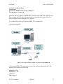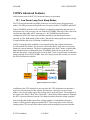
1
XYZ User’s Manual Version 0.1 Work In Progress Embedded Networks and Applications Lab (ENALAB) Yale University XYZ Team Dimitrios Lymberopoulos Andrew Barton-Sweneey Quentin Lindsey Andreas Savvides For an updated version of this manual please visit the XYZ website http://www.eng.yale.edu/enalab/XYZ ACKNOWLEDGMENTS: National Science Foundation (NSF) Cogent Computer Systems, Inc. OKI Semiconductor ARM Ltd NESL SOS team @ UCLA Report changes or errors at: [email protected] ENALAB YALE UNIVERSITY 1. 2. 3 Introduction................................................................................................................ 4 XYZ Feature Set ........................................................................................................ 5 XYZ Programming Tools Installation ....................................................................... 7 3.1 Cygwin................................................................................................................ 7 3.2 ARM-GCC.......................................................................................................... 8 3.3 SOS operating System ........................................................................................ 8 3.4 Seehau Software for the Nohau In-Circuit Emulator.......................................... 9 3.4.1 Configuration of the Seehau Emulator ....................................................... 9 4 Basic Programming on XYZ ................................................................................... 12 4.1 File Structure..................................................................................................... 12 4.1.1 Building applications to run from FLASH or RAM................................. 13 4.2 Accessing the Registers – Basic Macros .......................................................... 14 4.3 GPIO Configuration.......................................................................................... 16 4.4 Configuring and Using Timers ......................................................................... 17 4.5 Configuring and Using External Interrupts....................................................... 19 4.6 Configuring and Using Peripherals................................................................... 20 4.7 An Example Application................................................................................... 21 4.8 Debugging applications on XYZ ...................................................................... 27 5 Testing the XYZ sensor node .................................................................................. 31 6 Testing an XYZ node using a pre-installed SOS binary image ............................... 31 6.1.1 Setup SOSSRV ......................................................................................... 32 6.1.2 Loading the Module.................................................................................. 32 6.2 Compiling and Installing an SOS Module on the XYZ.................................... 34 6.3 Compiling and loading an SOS BLANK Kernel on the XYZ.......................... 35 7 Connecting XYZ to the PC and the Web................................................................. 36 7.1 Radio ................................................................................................................. 36 7.2 UART................................................................................................................ 36 7.3 SOSBASE ......................................................................................................... 37 7.4 SOSSRV ........................................................................................................... 37 7.4.1 Invoke SOSSRV from the Command-line................................................ 37 7.5 Using the POKE Application............................................................................ 38 8 Introduction to the SOS Operating System.............................................................. 40 8.1 Dynamic Modules............................................................................................. 41 8.2 Bootloader......................................................................................................... 41 9 Basic programming in SOS ..................................................................................... 41 9.1 SOS Messaging Mechanism ............................................................................. 41 9.2 Using Timers in SOS ........................................................................................ 42 9.3 Sampling the Sensors in SOS ........................................................................... 42 10 Programming with SOS and Modules ..................................................................... 42 10.1 Function pointers .............................................................................................. 42 10.1.1 Subscribed functions................................................................................. 43 10.1.2 Provided functions .................................................................................... 43 10.1.3 How to call function pointers.................................................................... 43 10.2 Timer interface.................................................................................................. 44 10.3 Recommended programming model for device drivers.................................... 45 XYZ User Manual 9/16/2005 2 ENALAB YALE UNIVERSITY 10.4 Enabling the Watch Dog Timer ........................................................................ 45 10.5 Reading the on-board Sensors .......................................................................... 45 10.6 Setting the Real Time Clock ............................................................................. 47 11 Miscellaneous Features............................................................................................ 47 11.1 Radio Signal Strength Indicator RSSI and Link Quality Indicator (LQI) ........ 47 12 XYZ’s Advanced Features....................................................................................... 49 12.1 Low Power Long Term Sleep Modes ............................................................... 49 12.2 Enabling & Disabling Different Processor Peripherals .................................... 50 12.3 Radio Sleep Modes ........................................................................................... 50 12.4 Microcontroller Frequency Scaling .................................................................. 50 13 Wireless Network Protocol Support ........................................................................ 51 14 ChipCon License...................................................................................................... 51 15 XYZ Schematics ...................................................................................................... 52 16 XYZ Peripheral Boards & Support Software .......................................................... 56 16.1 XYZ Prototyping Board.................................................................................... 56 17.2 Ulrasound and Mobility Board ......................................................................... 58 17.3 Acoustic Processing Interface and Acoustic Signature Recognition................ 58 18 XYZ Errata............................................................................................................... 59 19 References................................................................................................................ 59 XYZ User Manual 9/16/2005 3 ENALAB YALE UNIVERSITY 1. Introduction The XYZ is a general-purpose sensor node designed for teaching and experimentation in networked embedded systems and sensor network applications. The goal of the XYZ architecture is to provide a wealth of peripherals and ample computation resources to facilitate rapid experimentation with sensor networks problems, especially with applications involving mobility. To reduce the fabrication cost for sensor boards and for instructional purposes, the main board of the XYZ sensor node also includes 3 sensors: a MEMs accelerometer, a temperature sensor and a light sensor. This manual provides a brief overview of how to get started with XYZ. It describes the tool chain setup, and documents the main XYZ hardware and software features. Our description assumes that the reader is familiar with the basics of microcontroller programming. Throughout the description, this manual provides a few hands-on examples to familiarize the user XYZ and its development environement. With the exception of a few embedded systems programming exercises, all XYZ software is released as part of the SOS operating system developed at NESL, UCLA. The majority of the code examples on the usage of the different XYZ features are written SOS. Features related to authoring low level drivers and some performance demanding applications are written in C. All the software development of XYZ is done using the ARM7TDMI GNU tool chain. Pointers to the pre-compiled tool chains are provided on the XYZ website. The latest updates, documentation and applications of XYZ are posted on the XYZ website at : http://www.eng.yale.edu/enalab/XYZ For the latest information on the SOS operating system visit the SOS website at: http://nesl.ee.ucla.edu/projects/SOS The XYZ node is available to the research community from Cogent Computer http://www.cogcomp.com For access to the most recent developments and discussions on the XYZ, become a member of the XYZ-users Mailing List: [email protected] Please visit the following webpage to join the list: http://mailman.cs.yale.edu/mailman/listinfo/xyz-users XYZ User Manual 9/16/2005 4 ENALAB YALE UNIVERSITY 2. XYZ Feature Set The main XYZ sensor board provides the following hardware features. • OKI Semiconductor ML67 series ARM THUMB microcontroller o Processor controlled clock speed 1.8 – 58MHz o 256KB FLASH, -32KB RAM, 2Mbit off-chip RAM • Chipcon CC2420 IEEE 802.15.4 radio (250kbps raw data rate) • A real-time clock circuitry for allowing ultra-low power long-term sleep modes • MEMs accelerometer • Light Sensor • Thermometer • A wide variety of microcontroller peripherals. • Powered by 3AA 1.2V rechargeable batteries The main software features include: • IEEE 802.15.4 Medium Access Control Protocol (ported from Chipcon’s implementation). • SOS Operating System including dynamic module support provided by NESL UCLA • The XYZ low power API • Identification of acoustic signatures on the XYZ An overview of the XYZ architecture is shown in Figure 1. The sensor node is powered by 3AA batteries. The voltage regulator and the supervisor circuitry are directly powered by the batteries. All the other chips on the node are powered from the on-board voltage regulator which can be enabled or disabled by the supervisor circuitry. The on-board voltage regulator provides two voltages: the 2.5V required by the core of the CPU and the 3.3V required by the I/O of the CPU and the radio. These two voltages are fed to the rest of the board through a power tracking interface that facilitates that is used to easily monitor the power consumption of the sensor node. Figure 1. The XYZ architecture XYZ User Manual 9/16/2005 5 ENALAB YALE UNIVERSITY The communication subsystem of the XYZ sensor node is the Chipcon CC2420 IEEE 802.15.4 compliant radio that is interfaced to the processor through the processor’s SPI interface. The processor can completely turn on/off the radio and reset it in hardware or in software while the radio is capable of sending interrupt signals to the processor. The sensor subsystem of the node consists of a light sensor, a temperature sensor and a 2-axis accelerometer. All the sensors, except the temperature sensor, which has a digital interface, are connected to the on-chip ADC of the processor. Two 30-pin connectors are used to facilitate interfacing external circuits and sensors to the node. All free GPIO pins and the pins of the processor’s peripherals and all the power voltages used on the XYZ are output on these connectors. An additional prototyping accessory board is provided for interfacing new sensor designs to XYZ. A mobility mechanism implemented as an accessory board allows the XYZ sensor node to move along a string. An H-bridge is used to convert the 3.3V logic of the processor to 5V logic that is necessary for moving a miniature-geared motor at a decent speed. Using this mechanism the sensor node can be attached to a string a move itself on both directions along the string. An external 2Mbit SRAM has been added to complement the internal 32KB of RAM of the CPU chip. An overview of the OKI ML67Q500x ARM microcontroller is shown in Figure 2. As it can be seen in Figure 2 a variety of peripherals are available including a 2channel DMA controller and 7 hardware timers. Figure 2. The OKI ML67Q500x ARM 7 microcontroller XYZ User Manual 9/16/2005 6 ENALAB YALE UNIVERSITY Figure 3 The XYZ sensor node module Although there are many possibilities for programming the XYZ node, the supported method is to program the onboard OKI ARM processor using the GNU toolchain and the SOS operating system. The SOS operating system [3] is a small, event-driven pseudo real-time operating system designed at UCLA/NESL to facilitate research in wireless sensor networks. SOS is comprised of a static OS kernel and a set of dynamic modules that act as application building blocks. Modules communicate with each other through kernel calls or messages, and they can be dynamically installed/uninstalled during the system lifetime. A detailed SOS tutorial can be found on the SOS website at: http://nesl.ee.ucla.edu/projects/sos/tutorial/ 3 XYZ Programming Tools Installation Before delving into the actual details of programming, we first provide a description of how to setup and test the XYZ node using a pre-compiled binary image of the SOS operating system. This manual assumes a Windows environment. Support for other environments will be added in the future. The XYZ platform is built around an ARM architecture microprocessor from OKI Semiconductor. The processor has built support for JTAG programming and remote debugging. The development of software for SOS and the XYZ requires the ARM-GCC compiler, GNU Tools and CYGWIN. 3.1 Cygwin The CYGWIN program is required by the GNU Tools and recommended for the SOS tools and provides a UNIX command line environment. The CYGWIN is available at http://www.cygwin.com XYZ User Manual 9/16/2005 7 ENALAB YALE UNIVERSITY The CYGWIN also provides useful support develop and deploy SOS sensor networks, including a CVS client, webserver and database. 3.2 ARM-GCC The ARM-GCC compiler tools from Code Sourcery are recommended for the XYZ. The ARM-GCC compiler is ANSI compliant and supports C++ and linking for the ARM architecture. The ARM-GCC tools are available at: http://www.codesourcery.com/public/gnu_toolchain/arm/2004-Q3D/arm-none-elf-2004q3d.exe The installation of the ARM-GCC tools is a standard windows-like installation. After installing the tools the environment variable PATH must be updated with the path to the executables just installed. Assuming that you have installed the tools under the folder: C:\Program Files\CSL Arm Toolchain\ then the following directory should be added to the PATH environment variable: C:\Program Files\CSL Arm Toolchain\bin. In order to set the PATH environment variable follow these steps: 1) Right click on “my computer” and choose “Properties”. 2) Choose the “Advanced” tab and click on the “Environment Variables” at the bottom of the window. 3) From the variables that appear, choose the variable PATH and at the end add the following: ;C:\Program Files\CSL Arm Toolchain\bin. After setting the environment variable PATH restart Cygwin so that the changes take effect. 3.3 SOS operating System The SOS Operating System is distributed by NESL at UCLA. SOS is available from the CVS repository. Snapshots of repository are listed from the SOS website. See the SOS documentation for more information on obtaining SOS. To view the SOS repository online go to, http://cvs.nesl.ucla.edu/cvs/viewcvs.cgi/sos/. The latest source code and documentation for SOS is available directly from the CVS. When prompted for password, enter "anon", $ export CVS_RSH=ssh $ export [email protected]:/Volumes/Vol1/neslcvs/CVS $ cvs co sos XYZ User Manual 9/16/2005 8 ENALAB 3.4 YALE UNIVERSITY Seehau Software for the Nohau In-Circuit Emulator The Seehau Emulator is an In-Circuit Emulator for the XYZ sensor node. It is not freely available and therefore it is not available for download on the XYZ website. The installation of the emulator is exactly the same with most of the window-based programs installations. 3.4.1 Configuration of the Seehau Emulator Before you use the Seehau Emulator you have to configure it. In order to configure the emulator select: START-> Program Files -> Seehau ARM -> Config. You will be asked to set the type of the JTAG and the type of the processor you use. Make sure that your selections match the selctions shown in Figure 4. Figure 4. Configuring the Seehau Emulator After setting the type of the JTAG and the processor used choose: NEXT. In the next screen you have to set the clock frequency for the JTAG. Set the clock frequency at 33MHz as shown in Figure 5 and click on FINISH. XYZ User Manual 9/16/2005 9 ENALAB YALE UNIVERSITY Figure 5. Setting the clock frequency At this point you finished the basic configuration of the emulator. The next message on your screen asks you if you want to start the emulator. First make sure that your JTAG is properly connected to the USB port of your PC and that is also connected to a poweredup XYZ sensor node and then choose YES. When connecting the JTAG to the XYZ sensor node make sure that you can see the small arrow on the JTAG connector that goes to the XYZ when you have a top view of the XYZ sensor node. A wrong connection between the JTAG and the XYZ might damage the XYZ, the JTAG or both! If everything was successful, you should be able to see whatever is shown in Figure 6. The main window of the seehau emulator shows the contents of the flash memory inside the OKI processor. As it is shown in Figure 6, all the addresses of the FLASH memory can be seen. Also, the contents of the registers and the RAM are also available to the user for reading and writing (the two remaining windows). XYZ User Manual 9/16/2005 10 ENALAB YALE UNIVERSITY Figure 6. Seehau emulator is up and running. In order to be able to load executable files into the FLASH you should go to: Config->Emulator and under the Misc Setup tab you should have the same settings as the ones shown in Figure 7. After changing the settings click on APPLY and then click on OK. In order to be able to place breakpoints into your code go to: Run-> Force Hardware Step. Now your Seehau Emulator has been fully configured. In order to save your new settings exit the Seehau emulator and save the setup file of the emulator by overwriting the existing one. For more information on how to use the Seehau emulator see section 4.8. XYZ User Manual 9/16/2005 11 ENALAB YALE UNIVERSITY Figure 7. Setting the Seehau emulator to load executables to the FLASH. 4 Basic Programming on XYZ The purpose of this section is to get you familiar with the low-level basic programming on the XYZ sensor node without an operating system. In the following subsections we will introduce a set of basic programming macros. We will also describe of how to access the registers and how to configure and use the timers, the interrupts and the GPIO pins is presented. The sample code for these examples can be found at: http://www.eng.yale.edu/enalab/XYZ/programming/pa1_code.zip 4.1 File Structure The necessary files for compiling XYZ applications along with a sort description are listed below: Makefile: application makefile. All the rules for compiling the application and the format of the output files are defined here. application.c: main application file containing user’s application. common.h: data type definitions and programming macros for register access. define.s: assembler common definitions file. init.s: Startup routine. XYZ User Manual 9/16/2005 12 ENALAB YALE UNIVERSITY irq.c: Interrupt handler’s initialization functions. irq.h: Interrupt handler’s basic function declarations and definitions (enable/disable interrupts etc). reentrant_irq.s: Reentrant interrupt handler routine. romarm.ld: Link command file for building programs. It contains the memory definition and defines where the program and the data will be stored. ml674001.h: Processor specific header file. All the CPU registers and MACROS for accessing them are defined in this file. The main application file can be renamed from application.c to anything_else.c as long as the Makefile is modified accordingly. The only change required in the Makefile is in the object filename from application.o to anything_else.o. In the case where more than one application files are needed (for instance: application1.c, application2.c etc) then the corresponding object files (application1.o, application2.o etc) should be added in the “OBJS = irq.o reentrant_irq.o init.o application.o ” line located in the Makefile. 4.1.1 Building applications to run from FLASH or RAM Assuming that all the necessary files, described above, are in the same directory and the application code is free of errors, the executable file can be obtained by typing the following commands in cygwin: $ make clean $ make If the application code is free of errors an executable file called application_rom.elf will be produced. By default this executable file is produced to run from FLASH. However, small changes in the linker file (romarm.ld) and the Makefile allow the produced executable to run from RAM. The linker file (romarm.ld) consists of two parts: the MEMORY part and the SECTIONS part. In the MEMORY part, the start address and the size of both the FLASH and the RAM are defined. MEMORY { rom (rx) : ORIGIN = 0x00000000, LENGTH = 256K ram (rx) : ORIGIN = 0x50000000, LENGTH = 32K } In the SECTIONS part, the final destination of the code and the data is defined among others. The .text section corresponds to the code and the .data section corresponds to the data of the application. The destination (FLASH or RAM) of the code and the data is defined at the end of the .text and the .data sections respectively, as follows: .text { …….. …….. XYZ User Manual .data { ……. ……. 9/16/2005 13 ENALAB YALE UNIVERSITY } > rom } > ram According to this configuration of the linker file, which is the default configuration, the application code will be stored in FLASH and the application data will be stored in RAM. In other words, the application will run from FLASH. In order to make the application run from RAM the .text section should be changed as follows: .text { ……. ……. } > ram and the line: elf: application_rom.elf in the Makefile should be replaced with the following: ram: application_ram.elf. Now, by typing: $ make clean $ make in cygwin, the executable file application_ram.elf is produced to run from RAM. 4.2 Accessing the Registers – Basic Macros All the basic data types and the macros for accessing the registers of the ARM processor are defined in the file: common.h. The most commonly used data types are the following: BYTE: signed 8-bit. UBYTE: unsigned 8-bit. HWORD: signed 16-bit. UHWORD: unsigned 16-bit. WORD: signed 32-bit. UWORD: unsigned 32-bit. The size of the internal CPU registers varies from 8-bit to 32-bit. Depending on the size of the register, different MACROS have been defined for reading/writing these registers: put_value(register_name, hex_value): write the 8-bit hex_value in the register called register_name. get_value(register_name): get the value of the 8-bit register called register_name. put_hvalue(register_name, hex_value): write the 16-bit hex_value in the register called register_name. get_hvalue(register_name): get the value of the 16-bit register called register_name. put_wvalue(register_name, hex_value): write the 32-bit hex_value in the register called register_name. get_wvalue(register_name): get the value of the 32-bit register called register_name. XYZ User Manual 9/16/2005 14 ENALAB YALE UNIVERSITY The [put_value(), get_value()], [put_hvalue(), get_hvalue()], and [put_wvalue(), get_wvalue()] pairs of macros should be used only with 8-bit, 16-bit and 32-bit registers respectively. For instance, if your application goal is the following: 1. Read the value of the 16-bit register GPPOB. 2. Write the value you read in the 16-bit register GPPOA. 3. Write the value 0x3C in the register WDTCON. then your application file should look like this: int main(void) { /* Unsigned 16-bit integer*/ UHWORD read_data; /* Read the 16-bit register GPPOB*/ read_data = get_hvalue(GPPOB); /*Write the 16-bit register GPPOA*/ put_hvalue(GPPOA, read_data); /*Write the 8-bit register WDTCON*/ put_value(WDTCON, 0x3C); return 0; } In many cases, it is desirable to set or clear independent bits of a register. Note that the macros presented so far automatically set all the bits in a register. In order to independently set or clear individual bits in a register, a separate set of MACROS is available: set_bit(register_name,2n ): set the n-th bit in the 8-bit register called register_name. clr_bit(register_name, 2n): clear the n-th bit in the 8-bit register called register_name. set_hbit(register_name, 2n): set the n-th bit in the 16-bit register called register_name. clr_hbit(register_name, 2n): clear the n-th bit in the 16-bit register called register_name. set_wbit(register_name, 2n): set the n-th bit in the 32-bit register called register_name. clr_wbit(register_name, 2n): clear the n-th bit in the 32-bit register called register_name. Note, that the second arguments in all of these macros is not the actual bit position but number 2 to the power of the bit position that has to be set or cleared. The right most bit in a register is considered to be bit 0 while the right most bit is considered to be bit 7, 15, or 31 depending on the size of the register. For instance, the following lines of code set bits 0 and 5 and clear bit 23 in the 32-bit register ILC1: set_wbit(ILC1, 0x00000001); /* Set bit 0 */ set_wbit(ILC1, 0x00000020); /* Set bit 5 */ XYZ User Manual 9/16/2005 15 ENALAB YALE UNIVERSITY clr_wbit(ILC1, 0x00800000); /* Set bit 23 */ 4.3 GPIO Configuration The OKI processor on the XYZ sensor node provides 5 GPIO ports that correspond to 42 GPIO pins. Ports A, B, C and D are 8-bit ports while port E is a 10-bit port. Each GPIO pin has a primary and a secondary function. By default the primary function of a GPIO pin is to act as general purpose input or output. The secondary function of a single or a set of GPIO pins is . A complete list of the GPIO pins and their secondary functions can be found in [5] (Chapter 13). The steps for configuring and using a GPIO pin as a general purpose input/output are the following: 1. Configure the GPIO pins to be used as their primary functions. This can be done by writing the appropriate value to the GPCTL register. Every bit in the GPCTL register controls a group of GPIO pins. Setting a bit in the GPCTL register to 1 configures the corresponding group of GPIO pins as their secondary function. Conversely, setting a bit in the GPCTL register to 0 configures the corresponding group of GPIO pins as their primary functions (general purpose I/O). In order to use a GPIO pin as a general purpose I/O pin you must first find the bit in the GPCTL register that corresponds to this pin and set it to 0. 2. After setting a GPIO pin as a general purpose I/O pin, the direction (input or output) of this pin must be defined. This can be done by writing the registers GPPMX, where X=A, B, C, D, or E. Each GPPMX register is a 16-bit register that controls the I/O directions of every pin that belongs in the port X. The least significant bit of the GPPMX register corresponds to port’s X GPIO pin 0. The 7th bit (ports: A, B, C, or D) or the 9th bit (port E only) correspond to the 8th and 10th bit respectively of the ports A through D and E. Setting a bit in this register to 1, configures the corresponding GPIO pin as output. Conversely, setting a bit in this register to 0 configures the corresponding GPIO pin as input. 3. If a GPIO pin is configured as output then the state of the pin can be changed by writing register GPPOX, where X=A, B, C, D, or E. The format of the GPPOX register is exactly the same with the format of the GPPMX register. Each bit of the GPPOX register corresponds to a GPIO pin that belongs in port X. Writing 1 to a bit will force the corresponding GPIO pin that is set as output, to become 1. Conversely, writing 0 to a bit will force the corresponding GPIO pin that is set as output, to become 0. In the case where a GPIO pin is configured as input, its state can be retrieved by reading the register GPPIX, where X=A, B, C, D or E. As before, each pin in this register corresponds to a GPIO pin. Reading this register corresponds to reading all the GPIO pins that are controlled by this register. As an example of configuring and using the GPIO pins as general purpose I/O pins consider the following application: 1. Set PIOA[0] as input and PIOA[1] as output. 2. Output 1 at PIOA[1] and read the value of PIOA[0]. 3. Turn on all the LEDs on the XYZ. The 3 LEDs are connected to pins PIOD[4], PIOD[5] and PIOD[7]. XYZ User Manual 9/16/2005 16 ENALAB YALE UNIVERSITY The code for this example application is the following: int main(void) { /* Unsigned 16-bit integer*/ UHWORD read_data; /* Configure pins PIOA[0] and PIOA[1] as their primary functions*/ clr_hbit(GPCTL, 0x0001); /* bit 1 controls the whole A port, PIOA[0:7]*/ /*Configure PIOA[0] as input*/ clr_hbit(GPPMA, 0x0001); /*Configure PIOA[1] as output*/ set_hbit(GPPMA, 0x0002); /*Output 1 at PIOA[1]*/ set_hbit(GPPOA, 0x0002); /*Read the value of PIOA[0]*/ read_data = get_hvalue(GPPIA); /*Read all pins in port A, PIOA[0:7]*/ read_data = read_data & 0x0001 ; /*Isolate pin PIOA[0]*/ /* read_data now contains the value of input pin PIOA[0] */ /*Turn on the LEDs. Pins PIOD[4:6] do not have a secondary function!*/ /* Configure pins PIOD[4:6] as outputs */ set_hbit(GPPMD, 16); /*PIOD[4]*/ set_hbit(GPPMD, 32); /*PIOD[5]*/ set_hbit(GPPMD, 64);/*PIOD[6]*/ /*Turn on the LEDs by writing 0 to PIOD[4:6]*/ clr_hbit(GPPOD, 16); clr_hbit(GPPOD, 32); clr_hbit(GPPOD, 64); return 0; } 4.4 Configuring and Using Timers The CPU chip supports a system timer and 6 dedicated hardware timers (TIMER0 through TIMER5). Applications that need accurate timing is recommended to use the dedicate hardware timers. Each of the 6 hardware timers has a set of configuration registers (more detailed information can be found in chapter 15 in [5]): TIMECNTL0-TIMECNTL5: Timer control register. This register is responsible for: o Defining the operating clock frequency of the timer. XYZ User Manual 9/16/2005 17 ENALAB YALE UNIVERSITY o Configuring the timer as one-shot timer or interval timer. o Starting or stopping the timer. o Enabling/Disabling the timer interrupts. TIMEBASE0-TIMEBASE5: Timer base register. The initial value of the timer counter. TIMECNT0-TIMECNT5: Timer counter register. The current value of the timer counter. TIMECMP0-TIMECMP5: Timer compare register. The “overflow” value of the timer .When the timer counter register becomes equal to the timer compare register a timer interrupt is fired. TIMESTAT0-TIMESTAT5: Timer status register. It indicates if a timer interrupt was fired or not. The procedure for configuring and using a timer (we assume TIMER0 here) is the following: 1. Stop the timer by clearing bit 3 in register TIMECNTL0. 2. Set the timer interrupt handler and set its priority level. Note that all interrupts have priority level 0 by default. In other words they are masked. In order to activate an interrupt a priority level higher or equal to 1 is required. 3. Set the operating clock frequency of the timer by writing bits 5 through 7 in register TIMECNTL0. 4. Set the mode of the timer by writing bit 0 in register TIMECNTL0. Every timer can be configured as an interval timer or as a one-shot timer. The one-shot timer gives only one interrupt and then it is disabled. Conversely, the interval timer periodically gives timer interrupts until it is stopped by the user by clearing bit 3 in register TIMECNTL0. 5. Write the initial value of the timer in the register TIMEBASE0. This is the value from which the timer counter will start counting. 6. Write the overflow value of the timer in the TIMECMP0 register. 7. Clear the status bit by writing 1 to bit 0 in register TIMESTAT0. 8. Enable interrupts by setting bit 4 in register TIMECNTL0. 9. Start the timer by setting bit 3 in register TIMECNTL0 to 1. Every time that the value of the TIMECNT0 register becomes equal to the value of the TIMECMP0 register, a timer interrupt will be fired and the timer interrupt handler will be called. If the timer is configured as a one shot timer the timer handler will be called only once. Conversely, if the timer is configured as interval timer the timer handler will be called repeatedly. Independently of the configuration of the timer, the timer interrupt handler should always clear the status bit of the timer before returning, otherwise future timer interrupts will be ignored. An example of an interval timer is the following: static void timer0_interrupt_handler() { /* Clear the status bit */ put_hvalue(TIMESTAT0, 1); …… …… } XYZ User Manual 9/16/2005 18 ENALAB YALE UNIVERSITY int main(void) { /* initialize interrupt handling */ init_irq(); // set timer interrupt handler IRQ_HANDLER_TABLE[INT_TIMER0] = timer0_interrupt_handler; /* Enable the interrupts */ ENABLE_GLOBAL_INT(); /* Set the timer interrupt priority level to 1 */ set_wbit(ILC, ILC_ILC16 & ILC_INT_LV1); /* set timer base value to 0 */ put_hvalue(TIMEBASE0, 0); /* set timer comparison value */ put_hvalue(TIMECMP0, 0xFFFF); /* set timer to interval mode */ clr_hbit(TIMECNTL0, TIMECNTL_INT); /* Clear the status bit */ put_hvalue(TIMESTAT0, 1); /* enable timer interrupts */ set_hbit(TIMECNTL0, TIMECNTL_IE); /* start timer */ set_hbit(TIMECNTL0, TIMECNTL_START); while(1){;} /* Do not return so that the timer interrupt handler is called! */ return 0; } 4.5 Configuring and Using External Interrupts Configuring and using external interrupts is very similar to using the timer interrupts. Detailed information on how to configure and use the external interrupts can be found in chapter 8 in [5]. DIMITRIS (I will finish this section) XYZ User Manual 9/16/2005 19 ENALAB 4.6 YALE UNIVERSITY Configuring and Using Peripherals The procedure for configuring and using the on-chip peripherals is almost the same for all the available peripherals. In general, the steps to use a peripheral are the following: 1. Find the GPIO pins whose secondary function is the peripheral you want to use. Configure these GPIO pins as their secondary functions by writing the appropriate values in the GPCTL register. 2. Write the configuration registers of the peripheral according to your application needs and use it! In this section, the configuration and usage of the SIO peripheral is demonstrated (a detailed description of the SIO peripheral can be found in chapter 17 in [5]). The GPIO pins that implement the SIO interface as a secondary function are pins PIOB[6] and PIOB[7]. The configuration registers for the SIO peripheral are the following: SIOBUF: This register holds transfer data (either sent or received data). SIOSTA: Status register. It indicates errors in transmission and provides “ready” flags for transmitter and receiver. SIOCON: Control register. It specifies the frame format for data transfers. SIOBCN: Baud rate control register. It starts and stops the baud rate timer counter. SIOBT: Baud rate timer register. The value of this register sets the baud rate. For more information about setting the baud rate please see chapter 17 in [5]. An example application where the SIO interface is configured and used to send a byte is presented below. void configure_SIO(void); /* Configuration of the SIO interface */ void output_byte(int); /* Send a byte through the SIO interface */ int main(void) { configure_SIO(); /* Configure the SIO interface */ output_byte(0xF0); /* Send a byte */ return 0; } void configure_SIO(void) { /*Configure pins PIOB[6] and PIOB[7] as their secondary functions */ put_wvalue(GPCTL, GPCTL_SIO); /* Specify the frame format: 8 data bits, parity is disabled, 1 stop bit */ put_wvalue(SIOCON, 0x000C); /* Set the baud rate */ XYZ User Manual 9/16/2005 20 ENALAB YALE UNIVERSITY put_wvalue(SIOBT, 162); /* Start the SIO interface */ put_wvalue(SIOBCN, 0x0010); } void output_byte(int outputByte) { long int sio_status; short transfer_ready; put_wvalue(SIOBUF, outputByte); /* Send the byte */ do { sio_status = get_wvalue(SIOSTA); /* Check the status register */ transfer_ready = (sio_status % 64) >> 5; } while (!transfer_ready); /* Check if the transmission is finished */ /* Clear the status bit */ put_wvalue(SIOSTA, sio_status | 0x0020); } 4.7 An Example Application In this section an example application is presented that demonstrates the use of several peripherals on the XYZ sensor node. The goal of the application is to sample the onboard light sensor every 5 seconds. Based on the value sampled each time, the application outputs a specific pattern on the onboard LEDs. In addition, the application outputs to the UART port the value that was sampled each time. The configuration and use of the hardware timers, the on-board ADC and the UART is demonstrated in this application. In order to test this application, replace the application.c file the code fragment at the end of this paragraph. Compile the application and load the application on the XYZ using the JTAG. Using a male-to-female RS232 cable, connect XYZ’s RS232 port to the RS232 port on your PC. On the PC side you can use a program like Teraterm to establish communication through the serial port. The settings on your serial port program running on the PC side should be the following: Baud rate: 58600 Data bits: 8 Stop bits: 1 Flow control: None #include "ML674001.h" #include "common.h" XYZ User Manual 9/16/2005 21 ENALAB YALE UNIVERSITY #include "irq.h" // 58 * 10^6 / (32 * TMR0_CMP * TMR0_COUNT) = 5 seconds #define TMR0_CMP 12500 #define TMR0_COUNT 725 #define DISABLE_GLOBAL_INT() do{ irq_dis(); } while(0) #define ENABLE_GLOBAL_INT() do{ irq_en(); } while(0) /* Globals: */ long int interval_count; /* define functions: */ void configure_SIO(void); void configure_ADC(void); void configure_timer(void); static void set_timer(unsigned long interval); static void timer0_interrupt_handler(); void output_byte(int outputByte); void configure_leds(void); void light_leds(int value); int main(void); /******************************************************************/ /* Configures SIO */ /* Function : configure_SIO */ /* Parameters */ /* Input : Nothing */ /* Output : Nothing */ /******************************************************************/ void configure_SIO(void) { put_wvalue(GPCTL, GPCTL_SIO); put_wvalue(SIOCON, 0x000C); put_wvalue(SIOBT, 162); put_wvalue(SIOBCN, 0x0010); } /******************************************************************/ /* Configures ADC */ /* Function : configure_ADC */ /* Parameters */ XYZ User Manual 9/16/2005 22 ENALAB YALE UNIVERSITY /* Input : Nothing */ /* Output : Nothing */ /******************************************************************/ void configure_ADC(void) { put_wvalue(ADCON2, 0x0003); /* CCLK / 8 */ put_wvalue(ADINT, 0x0000); /* Disable Interrupts */ put_wvalue(ADCON1, (get_wvalue(ADCON1) & 0xFFFC)); /* set channel 0 */ } /******************************************************************/ /* Configures Timer0 */ /* Function : configure_timer */ /* Parameters */ /* Input : Nothing */ /* Output : Nothing */ /******************************************************************/ void configure_timer(void) { DISABLE_GLOBAL_INT(); /* critical section */ IRQ_HANDLER_TABLE[INT_TIMER0] = timer0_interrupt_handler; set_wbit(ILC, ILC_ILC16 & ILC_INT_LV1); set_timer(TMR0_CMP); /* set timer interval */ ENABLE_GLOBAL_INT(); put_wvalue(TMEN, 0x01); /* enable timer */ } /******************************************************************/ /* Sets the timer0 interval */ /* Function : set_timer */ /* Parameters */ /* Input : interval */ /* Output : Nothing */ /******************************************************************/ static void set_timer(unsigned long interval) { /*shut it down */ put_wvalue(TIMECNTL0, (get_wvalue(TIMECNTL0) & 0xFFE7)); put_wvalue(TIMECMP0, interval); /* set comparison val */ put_wvalue(TIMEBASE0, 0x0000); /* set base timer val */ XYZ User Manual 9/16/2005 23 ENALAB YALE UNIVERSITY put_wvalue(TIMECNTL0, (get_wvalue(TIMECNTL0) & 0xFFF7)); /* set divisor */ put_wvalue(TIMECNTL0, (get_wvalue(TIMECNTL0) | 0x00A0)); /* enable interrupt & start timer */ put_wvalue(TIMECNTL0, (get_wvalue(TIMECNTL0) | 0x0018)); return; } /******************************************************************/ /* What to do when Timer0 interrupts */ /* Function : timer0_interrupt_handler() */ /* Parameters */ /* Input : Nothing */ /* Output : Nothing */ /******************************************************************/ static void timer0_interrupt_handler() { int i; long int ADC_interrupt_reg; long int ADC_done; long int light_reading; int leading_zeros_flag; int output[5]; if (interval_count == 0) { interval_count = TMR0_COUNT; /* turn on ADC */ put_wvalue(ADCON1, (get_wvalue(ADCON1) | 0x0010)); do { ADC_interrupt_reg = get_wvalue(ADINT); ADC_done = (ADC_interrupt_reg % 4) / 2; } while (!ADC_done); /* wait for conversion */ light_reading = get_wvalue(ADR0) % 1024; put_wvalue(ADINT, 0x0002); put_wvalue(ADCON1, (get_wvalue(ADCON1) & 0xFFEF)); /* turn off ADC */ XYZ User Manual 9/16/2005 24 ENALAB YALE UNIVERSITY if (light_reading < 300) light_leds(1); else if (light_reading < 700) light_leds(3); else light_leds(7); for (i = 0; i < 5; i++) /* calculate the digits in base 10 */ { output[i] = light_reading % 10; light_reading = light_reading / 10; } leading_zeros_flag = 1; for (i = 4; i >= 0; i--) /* output the digits in base 10 */ { if (output[i] != 0) leading_zeros_flag = 0; if (!leading_zeros_flag) output_byte('0' + output[i]); } output_byte('\r'); output_byte('\n'); } else { interval_count--; } put_wvalue(TIMESTAT0, 0x01); /* clear the interrupt bit */ } /******************************************************************/ /* Outputs a Byte over the serial port */ /* Function : output_byte */ /* Parameters */ /* Input : outputByte */ /* Output : Nothing */ /******************************************************************/ void output_byte(int outputByte) { long int sio_status; short transfer_ready; put_wvalue(SIOBUF, outputByte); do { sio_status = get_wvalue(SIOSTA); transfer_ready = (sio_status % 64) >> 5; } while (!transfer_ready); put_wvalue(SIOSTA, sio_status | 0x0020); } XYZ User Manual 9/16/2005 25 ENALAB YALE UNIVERSITY /******************************************************************/ /* Configures the GPIO D port for LED usage */ /* Function : configure_leds */ /* Parameters */ /* Input : Nothing */ /* Output : Nothing */ /******************************************************************/ void configure_leds(void) { /*make them outputs*/ put_wvalue(GPPMD, (get_wvalue(GPPMD) | 0x00E0)); /* turn them off */ put_wvalue(GPPOD, (get_wvalue(GPPOD) | 0x00E0)); } /******************************************************************/ /* Lights Up the LEDs according to the argument led_val */ /* Function : light_leds */ /* Parameters */ /* Input : led_val */ /* [0x111 -> all on] */ /* [0x100 -> red on] */ /* [0x010 -> green on] */ /* Output : Nothing */ /******************************************************************/ void light_leds(int led_val) { long int gppod_val; led_val = led_val % 8; /* make sure its only 3 bits */ gppod_val = ((led_val % 4) << 1) + (led_val >> 2); /* fix schematic error*/ gppod_val = gppod_val << 5; /* shift to correct pins */ /* write to GPIO D port */ put_wvalue(GPPOD, (get_wvalue(GPPOD) | 0x00E0) - gppod_val); } /******************************************************************/ /* Entry point */ /* Function : main */ /* Parameters */ XYZ User Manual 9/16/2005 26 ENALAB YALE UNIVERSITY /* Input : Nothing */ /* Output : 0 */ /******************************************************************/ int main(void) { configure_leds(); /* configure the LED registers */ configure_timer(); /* configure the Timer0 registers*/ configure_ADC(); configure_SIO(); interval_count = TMR0_COUNT; ENABLE_GLOBAL_INT(); /* enable interrupts */ while(1); return 0; } 4.8 Debugging applications on XYZ The Seehau Emulator facilitates the debugging of your applications on the XYZ sensor node. For moreinformation on how to install and configure the Seehau emulator see section 3.8. As it was mentioned in the previous subsections the output of the make command is an ELF type executable file. The executable is loaded into the FLASH memory of the XYZ sensor with a JTAG programmer. The JTAG programmer provides a useful debugging environment and allows using break points and single stepping through the program on the sensor node. So far we have tested 2 JTAG interfaces, one from Nohau and one from Macraigor system. The Nohau JTAG pod requires the Seehau debugger and runs under windows. The Macraigor Raven pods are lower cost devices that work with GDB, and can operate on Windows and Linux platforms. The drawback of the current version of the Macraigor interface is that it does how have any Flash programming software. Macraigor systems is considering the development of a Flash programmer designed specifically for XYZ. Assuming that you have followed the instructions given in section 3.8, when you start the Seehau emulator while the JTAG is connected to both the PC and a powered up XYZ sensor node you should be able to see something similar to figure 6 (page 11). In order to load an executable file to the flash you have to go to: FILE->LOAD and select the executable ELF file that you want to run. The Seehau emulator will automatically erase the whole FLASH and then it will reprogram the XYZ sensor node. Hitting the GO button will result in the execution of your application. You can stop the execution of your application at any time by hitting the STOP button. If instead of the GO button you hit the STEP IN TO button then the first line of code in the main function will be executed and the execution will be stopped as shown in Figure 8. XYZ User Manual 9/16/2005 27 ENALAB YALE UNIVERSITY Figure 8. Stepping into the code. Every time you hit the STEP INTO button another instruction is executed and the execution is stopped. When the program is running from the flash the user can also place breakpoints anywhere in his code and hit the GO button. The execution will be automatically stopped when it reaches a breakpoint. A maximum number of two breakpoints is allowed. User can set breakpoints anywhere in his code. By simply opening a source code file (FILE->OPEN FILE) and clicking on the left side of each line in the code users can place a breakpoint. Breakpoints can be placed only in lines of code that have a blue dot on the left side. If a line of code does not have a blue dot on the left side in the Seehau emulator’s editor then this means that this line of code is independent of the actual executable running on the XYZ node. When a user places a breakpoint in a line of code, the left part of that line becomes red as it can be seen in Figure 8 where a breakpoint has been set in line 218. By clicking the GO button the program will be executed and it will stop when it reaches the breakpoint as it can be seen in Figure 9. Note that the red color has been changed to pink indicating that this breakpoint forced the execution to stop. By clicking on the breakpoint again, the breakpoint is cleared. When the user is stepping through his code and the execution is stopped, he has the ability to read and write all the internal registers of the processor as it can be seen in Figure 10. In order to see the contents of the registers go to: VIEW -> S F Regs. XYZ User Manual 9/16/2005 28 ENALAB YALE UNIVERSITY Furthermore, when the execution is stopped the user can see the values of all the local variables. This can be done by selecting: VIEW->LOCAL VARIABLES. A list with the local variables will appear as it can be seen in Figure 11. Figure 9. Using the breakpoints. XYZ User Manual 9/16/2005 29 ENALAB YALE UNIVERSITY Figure 10. Viewing the internal registers of the processor. XYZ User Manual 9/16/2005 30 ENALAB YALE UNIVERSITY Figure 11. Viewing the local variables. 5 Testing the XYZ sensor node A precompiled executable file called blink_test.elf can be found on the XYZ website (http://www.eng.yale.edu/enalab/XYZ). Download the executable file and load it on the XYZ sensor node as it is described in section 4.8. 6 Testing an XYZ node using a pre-installed SOS binary image Assuming that the SOS kernel is already loaded on the XYZ, we will use the SOS server application, SOSSRV, running on a PC to install a pre-compiled binary module that blinks the LEDs on a set of XYZ nodes. SOSSRV communicates with an XYZ node. To install the module on an XYZ follow the steps below: 1. Connect the XYZ to the serial port of your PC. 2. Open a new Cygwin shell. XYZ User Manual 9/16/2005 31 ENALAB YALE UNIVERSITY 3. Launch the SOS server. 4. Open another Cygwin shell. 5. Start the modd_gw client application to insert the module into SOS. 6.1.1 Setup SOSSRV The SOSSRV tool allows the sensor network to communicate through the serial port of a PC and over the Intranet or Internet. Build the SOSBASE application and load the program onto the SOSBASE. Build the SOSSRV tool on the computer connected to the SOSBASE and start the program. $ cd sos-1.x/tools/sos_server/bin $ make clean $ make $ ./sossrv.exe -s /dev/ttyS0 Figure 12 The XYZ sensor node connected to the PC and SOSSRV. 6.1.2 Loading the Module The SOS file for a module is loaded in the sensor network through the MODD_GW program. The MODD_GW program is an SOS module that runs on the host PC and communicates with the sensor network through SOSSRV. After SOSSRV is setup, set the path to include the MODD_GW program and run the program with the proper options to connect to the SOSSRV or use the default options. The MODD_GW accepts three commands from user: insmod, rmmod and debug. The commands are entered as the module id +1000 followed by the command name followed by options for the command. To load the blink module, copy the blink.sos file into the directory of the MODD_GW program. Start MODD_GW and use the insmod command to load the module. Use the rmmod command to unload the module and the debug command to enable debugging output. See the SOS documentation for more information about MODD_GW. XYZ User Manual 9/16/2005 32 ENALAB YALE UNIVERSITY $ cd sos-1.x/config/modd_gw $ make clean $ make emu ADDRESS=65534 SOS_GROUP=1 $ ./modd_gw.exe –a sossrv-ip Make sure the SOS_GROUP of the MODD_GW is the same as the SOS_GROUP of the kernel running the XYZ nodes. See the section on compiling and loading a kernel for more information about setting the SOS_GROUP. To load the SOS module, type into the MODD_GW command line, 1136 insmod blink.sos Figure 13 The setup for loading modules onto the XYZ using MODD_GW. At this point MODD_GW will print the status of the module loading to the shell. The output will be similar to the following: module id = 128 memory size = 24 version = 4 addr_start = 0 XYZ User Manual 9/16/2005 33 ENALAB YALE UNIVERSITY addr_end = 233 simulate fix_address... ***Flash buffer write page 192, addr = 49152 loading complete, sending advertiment to network The SOSSRV program will receive a message from the MODD_GW and print something similar to the following: --- Received from Desktop --Dest Mod Id: 14 Src Mod Id: 136 Dest Addr : FFFF Src Addr : 92 Msg Type : 13 Msg Length : 5 Msg Data: 80 4 E9 0 1 CRC: 0 0 To remove a module, use the rmmod command followed by the name of the module: 1136 rmmod blink.sos To enable debugging output from MODD_GW, enter the command: 1001 debug on To suppress debugging output from MODD_GW, enter the command: 1001 debug off The MODD_GW command will install a module the module on SOS on the XYZ node by writing the module to the OKI/ARM processor FLASH and start executing it. At the same time, the default loader module of SOS will propagate the new module to all the XYZ nodes within radio range. This happens with a process that advertises the existence of a new module to nearby nodes. Neighboring nodes that do not have the module will respond to the advertising node requesting the new module. All nodes that run the new module should now be blinking their LEDs. If the LEDs are blinking, the module was successfully installed and your XYZ nodes are functioning correctly. 6.2 Compiling and Installing an SOS Module on the XYZ The Blink application demonstrates the basic principles of the SOS sensor network. Set the path to the blink module directory and build the module. $ make clean $ make xyz XYZ User Manual 9/16/2005 34 ENALAB YALE UNIVERSITY $ make install2 Do not specify an address or other kernel specific options for the build of the module. The build process generates a file blink.sos that is the loadable module image. The install2 target to make copies the module image to the MODD_GW directory. Follow the procedure described in the section on the loading a precompiled module image for instructions on how to load the module onto the XYZ. 6.3 Compiling and loading an SOS BLANK Kernel on the XYZ The kernel is compiled as a static executable image and loaded onto the XYZ using a JTAG programmer. Some modules may be included in the compilation of the kernel and loaded onto the XYZ through the JTAG without using the MODD_GW program. The build of the kernel image is controlled by the file called Makerules in the config directory. See the SOS documentation for more information on building static applications. To compile a blank kernel use the following commands, $ cd sos-1.x/config/sos_blank $ make clean $ make xyz ADDRESS=1 SOS_GROUP=1 The ADDRESS sets the address of the node. The SOS_GROUP sets the group number of the nodes. Make sure that each node has a unique address and that groups of nodes share the same SOS_GROUP number. See the section on Loading the executable with the JTAG for instructions on loading the static kernel image onto the XYZ. Make sure to build a new image with a unique address for each XYZ node. XYZ User Manual 9/16/2005 35 ENALAB YALE UNIVERSITY 7 Connecting XYZ to the PC and the Web The sensor network of XYZ nodes running SOS is designed to easily connect to a PC and the Internet for configuration of the network, sensing and control applications. The communication inside the sensor network relies on the radio that is integrated into every XYZ node. The sensor network is linked to the PC by a serial data link. An XYZ that is configured as an SOSBASE has an integrated UART and is connected to the PC. The SOSBASE application allows the PC to send and receive SOS messages over the UART and forward the message to a routing module or directly to the radio and the neighbors within one-hop radio range. The PC runs the SOSSRV application to manage to the UART and the SOSBASE and provide an standard interface for client applications to access the sensor network. 7.1 Radio The Kernel on the XYZ uses the IEEE 802.15.4 Radio built into the XYZ platform for messaging with the sensor network. The physical layer of the IEEE 802.15.4 radio is implemented on the CC2420 radio chip and operates at 2.4GHz. The CC2420 has 24 channels and 7 power selectable power levels. The MAC layer of the IEEE 802.15.4 radio is implemented in software on the XYZ. The MAC layer is ported from the IEEE 802.15.4 MAC developed by ChipCon. The radio packs SOS message structures in the IEEE 802.15.4 packets. The maximum length of an SOS message is 256 bytes. 7.2 UART The XYZ platform has a built in UART for serial port communications with a PC. The UART uses a MAX232 level conversion chip to generate RS232 voltage levels. See the XYZ schematic for the pins used by the UART. A package is available for the XYZ sensor that integrates the serial port DB9 connector for the UART on the sensor node. Connect the XYZ sensor to the PC with a male-to-female DB9 cable. The XYZ is capable of outputting a single direction stream of text to the serial port and PC or using a bidirectional UART protocol to transfer SOS messages to from the sensor to the PC and from the PC to the sensor. The single direction text stream is called a raw stream and contains no SOS messages headers. The support for the raw stream is compiled into the static kernel image by including the definition in the Makefile of the kernel image, DEFS += -DUSE_UART_RAW_STREAM. The raw stream disables the sensor from running the SOSBASE application. The text is sent to the UART by calling the ker_uart_send() command. The SOSBASE application enables the UART messaging support that provides bidirectional communication over the UART with the PC. The SOSSRV program is run on the PC and forwards the messages from the sensor node clients and from the clients to the sensor node. The SOSBASE program forwards the UART messages to the sensor network without processing. Messages from the sensor network are received by the XYZ User Manual 9/16/2005 36 ENALAB YALE UNIVERSITY SOSBASE and forwarded to the SOSSRV without processing. A checksum is appended to the SOS messages over the UART and verified at the receiving end. 7.3 SOSBASE The SOSBASE is an XYZ sensor with the SOSBASE static application. The SOSBASE acts as an interface between the wireless sensor network and the host PC. The XYZ sensor is available in a package for running a SOSBASE. The power supply for the SOSBASE provides +5VDC. WARNING: if you use a different power supply you risk destroying the XYZ sensor. The SOSBASE has a DB9 connector built into the package. Connect the XYZ sensor to the PC with a male-to-female DB9 cable. The address of the SOSBASE application must be different from the address of the programs running on the host PC. 7.4 SOSSRV The SOSSRV tool allows the sensor network to communicate through the serial port of a PC and over the Intranet or Internet. The SOSSRV program transmits messages between sensor nodes in the network and programs running on the host PC. The programs on the PC connect to SOSSRV through TCP or UDP sockets. The SOSSRV requires an XYZ configured as a SOSBASE connected to a serial port on the PC. To install SOSSRV, follow the instructions in the section “Testing an XYZ node using a pre-installed SOS binary image”. Make sure the PC is connected to an XYZ that is configured as an SOSBASE. 7.4.1 Invoke SOSSRV from the Command-line The SOSSRV program accepts a few of command line options to configure the server port and the serial port. The following are the command line options for SOSSRV: sossrv [-p <Port>] [-s <COM Port>] [-n <TCP Port>] [-b <baudrate>] [-h] -p <Port> The port number of the sossrv server. (Default = 7915) -s <COM Port> SOSBASECOM Port.COM Port can be local device e.g. /dev/ttyUSB0 (Default = /dev/ttyS0) -n <TCP Port> TCP Port can be <IP Addr:Port Num> e.g. 192.69.10.3:6009 -b <baudrate> SOSBASE Baudrate. (Default = 57600 bps) -h Print this help message The SOSSRV program uses built-in default options for the server port and serial port if they are not specified on the command line. On Windows computers, the COM1 corresponds to /dev/ttyS0 and the numbers increase respectively. The SOSSRV program can run directly from a shell or the Windows Start Menu. To exit the program, type, <Ctrl-C> XYZ User Manual 9/16/2005 37 ENALAB YALE UNIVERSITY to the SOSSRV shell. The SOSSRV can run as a background process. The most effective way to run SOSSRV in the background is by using ssh to log into the host PC and type the following command, $ nohup ./sossrv.exe [options] & This allows the SOSSRV to continue running in the background after the user logs off. The output of the SOSSRV is saved in the file nohup.out in the directory of the SOSSRV program. The SOSSRV can be stopped by sending a signal to the SOSSRV process. In CYGWIN, use the following command to find the pid of the SOSSRV process, $ ps –e | grep sossrv Use the kill command to send a signal to the SOSSRV process as follows, $ kill <pid> where pid is the pid of the SOSSRV process. For more information on the nohup, ps and kill commands see the info and man pages. 7.5 Using the POKE Application Poke is a client application running on a PC that interacts with the SOS server to communicate with the sensors in the wireless sensor network. The poke command reads a poke script (*.pk) from the standard input and writes the result of the poke as a poke script to the standard output. The poke script contains a sequence of sos messages. The first part of an sos message is the version of sos (ex. SOS: 1 0 is sos-1.0). Poke can be invoked from the command line as follows: poke -h hostname [-v -p port -w delay -t timeout -c count -d daddr -s saddr -m sid] The command line options to poke control how the messages are sent and received. -v -h -p -w -t -c -d -s -m Enables debugging output.(default: off) Set hostname of the sos server. (default: none! must be specified) Set port for the sos server. (default: 7915) Set amount of time to wait between sending messages in seconds. (default: 0) Set timeout value while waiting to receive a message. (default: 1) Set maximum number of messages to receive. (default: 1) Set destination address in outgoing messages. (default: 2) Set source address in outgoing messages. (default: 1) Set source pid in outgoing messages. (default: 128) The following example reads a sequences of sos messages from the file example.pk and sends the messages to the sos server at localhost and the default port. The delay between the outgoing messages is 1 second. The timeout for incoming messages is 2 seconds. The XYZ User Manual 9/16/2005 38 ENALAB YALE UNIVERSITY maximum number of messages to receive is 4. The received messages are appended to the reply.pk file. $ poke -h localhost -w 1 -t 2 -c 4 < example.pk >> reply.pk The following is an example of a poke script. The SOS version field must be the first line of the message header. The order of the remaining lines in the message header is not important. The length field specifies the length of the data payload. The data is not required if the length of the message is 0. The values in the data payload begin after a line the contains the word DATA and are separated by white space, including spaces, tabs and new-lines. A line that starts with a period '.' character delimits the end of the header section of a message. The last line of the data section may optionally contain the crc values of the data. If the crc values are specified, they will terminate the data section. If the crc values are not specified, the a line that starts with a period '.' character is required to delimit the end of the data section. The data values are read from left to right. SOS: 1 0 DADDR: 2 SADDR: 1 DID: 156 SID: 128 TYPE: 33 LEN: 4 . DATA: 12 34 CRC: . The following shows a partial message. Poke will fill in the missing values for DADDR, SADDR and SID. Poke will try to use values from the command-line. If the values are not specified, then the default values are used. If a value is specified both in the message and on the command-line, the command-line value will override the vlaue in the message. SOS: 1 0 DID: 156 TYPE: 33 LEN: 4 . The poke command can be used as a sub-component within higher levels scripts to integrate communication with sensors. The poke command can also accept inline message definitions using the "here" document syntax available in most shells. The following example demonstrates an inline message definition. XYZ User Manual 9/16/2005 39 ENALAB YALE UNIVERSITY $post -h localhost <<EOF >SOS: 1 0 >SADDR: 65534 >DADDR: 3 >SID: 128 >DID: 157 >TYPE: 32 >LEN: 0 >. >EOF 8 Introduction to the SOS Operating System SOS is an open-source operating system specifically developed for driving small wireless sensor nodes. Before reading this section, the reader is encouraged to read the SOS tutorial available on the SOS website at: http://nesl.ee.ucla.edu/projects/SOS The Kernel provides a number of basic services to the application software. Some important services are the Scheduler, Timers, Radio, UART and ADC. See following sections for more information on the interfaces for XYZ platform. The SOS provides a standard API for application code to interact with the XYZ platform. The API increases the portability of the application code. The Kernel also provides the moduled, which is used for dynamically loading module images over the network. The kernel software is located in the kernel directory in the source tree from the CVS. The kernel directory contains all of the C code that is used to make the core kernel common on all platforms and processors. For more information about SOS see the doc directory in the source tree from the CVS. The files in the include directory in the source tree from the CVS describe the core API provided by SOS. The application code is located in sections of code called Modules. The modules can contain message handlers that implement the messaging protocols of algorithms in the sensor network. The modules communicate to each other by sending messages with a sensor destination address, the module pid and the message type. The modules can also provide functions to other modules for similar to a shared library. The separation and organization of the application code into related and modular sections aids the code development and portability. The modules software is located in the modules directory in the source tree from the CVS. The software that is specific to the XYZ node is located in the xyz directory inside the platform directory in the source tree from the CVS. The software that is specific to the OKI processor is located in the oki directory inside the processor directory in the source tree from the CVS. XYZ User Manual 9/16/2005 40 ENALAB YALE UNIVERSITY Tools for configuring the sensor network are located in the tool directory in the source tree. This consists of PC tools used with SOS including: the sos server, tools for automated testing of the code base, and the SOS GUI. 8.1 Dynamic Modules The SOS operating system supports dynamically loadable modules. The modules are important for maintaining the sensor network and developing software for the network. As sensor network increase in size and complexity, network maintenance and debugging becomes more critical and difficult. Intermittent bugs will occur in the deployment of large and long-term sensor networks. Large networks and extreme environments require remote management of the sensor network. The dynamic modules allow fixing bugs in the software and quickly update programs without disturbing the sensor network installation. The dynamic modules improve the process of developing software for the sensor network and allow researchers to test their program in-situ of the sensor network. 8.2 Bootloader The kernel and the module loader code running in the kernel implement the bootloader that is required to load the module in the FLASH program memory of the sensor nodes in the network and execute the program. See the SOS documentation for the module loader protocol. The module loader propagates module images and updates through the network. The module images are loaded into memory and integrated into the scheduler without restarting the sensor. The module loader and the kernel resolve the references between module code and the kernel code after the module is loaded on the sensor node. The modules interact asynchronously through message passing and synchronously though function pointers. The function pointers for kernel code are stored in the kernel jump table in the image of the static kernel. The function pointers for module code are stored in the function pointer table, and registered dynamically after the module is loaded into memory. The linkage to the module handlers are stored with the modules in FLASH and scanned in the module handler table in RAM at the startup of the sensor node. 9 Basic programming in SOS Andrew this section is yours… 9.1 SOS Messaging Mechanism Explain the notion of messages in SOS Mention the INIT and FINAL messages Mention how you can define your own messages. Explain the SOS messaging mechanism: post_net(). How can you send a message in a module on the same node and how you can send a message through the radio? XYZ User Manual 9/16/2005 41 ENALAB 9.2 YALE UNIVERSITY Include a simple example where you use your own message types and send messages to other modules on the same node and on other nodes. Using Timers in SOS Explain the interface that SOS provides for starting/stopping timers. 9.3 Sampling the Sensors in SOS Explain the SOS sensor interface... 10 Programming with SOS and Modules In SOS each module has a header to describe the functionalities it uses and provides. Here is one example from fnclient.c static const mod_header_t mod_header SOS_MODULE_HEADER = { mod_id: MOD_FN_C_PID, state_size: sizeof(fnclient_state_t), num_sub_func: 1, num_prov_func: 0, module_handler: module, funct: { {NULL, "Svv0", MOD_FN_S_PID, MOD_GET_NODE_ID_FID}, {NULL, "cCC2", MOD_FN_S_PID, MOD_SET_LED_FID}, }, }; mod_id is the module ID. State_size is the size of state module uses. Num_sub_func is the number of subscribed functions in this module. Num_prov_func is the number of provided functions. Module_handler is the function pointer pointing to module message handler. Funct is an array of data structure that describes the function pointer pointers. Every loadable module and kernel module that will use messaging are expected to declare the header. SOS ensures this header is placed in the program memory to save RAM space. 10.1 Function pointers XYZ User Manual 9/16/2005 42 ENALAB YALE UNIVERSITY Function pointers that module both uses and provides have to be declared in the module header. Subscribed functions are declared first followed by provided functions. Continuing the example in the previous section, there are four pieces of information that needs to fill in. They are function pointer to real implementation, function prototypes, module ID, and function ID. We separate the discussion into subscribed functions and provided functions. 10.1.1 Subscribed functions In subscribed functions, there are two types of subscription. One is static, which module specifies the function it will use at compile time; the other is dynamic, which module describes only the type information at compile time and subscribe function pointers at runtime. For static subscribed functions, Field 1: NULL Field 2: type encoding for the function prototypes Field 3: the module ID of the provider Field 4: the function ID of the provider For dynamic subscribed functions, Field 1: NULL Field 2: type encoding for the function prototypes Field 3: RUNTIME_PID Field 4: RUNTIME_FID 10.1.2 Provided functions For function providers, Field 1: the function pointer to real implementation Field 2: type encoding for the function prototypes Field 3: the module ID of this module Field 4: the function ID of this function 10.1.3 How to call function pointers To use a function, it is critical to include the function pointer in module state. For example, typedef struct { func_cb_t *get_id; func_cb_t *set_led; sos_timer_t timer; } fnclient_state_t; Above is the state declaration for the module described earlier. To use a function, one has to include a function pointer in the module state. The order of included function pointer in state is also critical as SOS will modify the pointer value during module insertion and when provider is removed. For example, get_id is the first function pointer XYZ User Manual 9/16/2005 43 ENALAB YALE UNIVERSITY included in module state, MOD_GET_NODE_ID_FID should be placed the first entry in the funct inside module header. To call a function, one needs to use the macro SOS_CALL. For example, SOS_CALL(s->set_led, func_i8u8u8_t, RED, TOGGLE); The first two parameters are fixed for all function calls. First parameter is the function pointer in the module state. The second parameter is a typedef to the real function pointers. It is expected that the function provider will do the typedef. For example, typedef int8_t (*func_i8u8u8_t)(char* proto, uint8_t arg0, uint8_t arg1); The first argument to the real function is always “char* proto”. This is used to recover from the failure when the provider does not exist. 10.2 Timer interface In SOS each module maintains its own timer data structure. That is, when module needs to use timer, it passes the pointer to timer data structure to kernel timer interface. To use the timer, module can either declare a sos_timer_t in module state or declare a pointer to sos_timer_t and ker_malloc at runtime. It is up to module write to make that decision. Before timer is first used, module should call, sos_timer_init(sos_timer_t *tt, sos_pid_t pid, uint8_t tid, uint8_t type) First argument is the pointer to timer data structure. Second argument is the module ID that uses the timer. Third argument is the timer ID. The last argument is the type of timer. This can be, TIMER_REPEAT TIMER_ONE_SHOT SLOW_TIMER_REPEAT SLOW_TIMER_ONE_SHOT The slow version is to post timeout event using low priority. To start a timer, one should call, ker_timer_start(sos_timer_t *tt, int32_t interval) Note that the timer interval or timeout value is specified here. This type of timer start has one failure condition when the timer is already started. To simplify typical use of timer, one can call ker_timer_restart(sos_timer_t *tt, int32_t interval) XYZ User Manual 9/16/2005 44 ENALAB YALE UNIVERSITY ker_timer_restart will restart the timer even when existing timer is already running. When one needs to stop the timer, one should call, ker_timer_stop(sos_timer_t *tt) 10.3 Recommended programming model for device drivers For device drivers that are never removed such as core SOS kernel components and low level hardware drivers, we suggest the following: Use static variables since it is more compact than dynamic memory. Use kernel version of module registration: sched_register_kernel_module( sos_module_t *handle, /* pointer to sos_module_t */ const mod_header_t *h, /* pointer to module header */ void *state_ptr) /* pointer to state variable */ This version of module registration is for static module only and does not involve any ker_malloc operation. Expose functionality through function pointer. Whenever there are additional functions to be provided, it is recommended to use function pointers. 10.4 Enabling the Watch Dog Timer Andrew (Do we really need this?) This is SOS independent!!!! 10.5 Reading the on-board Sensors All the on-board sensors, except the temperature sensor, are connected to the 4-channel ADC that is embedded on the OKI processor chip. Table 1 shows in detail how the onboard sensors are interfaced to the processor. On-board Sensor Light Accelerometer (x) Accelerometer (y) Temperature VBAT (3AA battery level) Interface ADC Channel #0 ADC Channel #1 ADC Channel #2 Digital: PIOE[5] (GPIO/External Interrupt) ADC Channel #3 Table 4. On-board sensor interfaces Any sensor that is connected to the ADC can be configured/read in two different ways: 1. Through the SOS ADC driver interface. 2. Directly, through accessing the CPU registers. XYZ User Manual 9/16/2005 45 ENALAB YALE UNIVERSITY The easiest way to access the light and accelerometer sensors is through the SOS ADC driver interface. The SOS functions that implement the ADC interface are the following: extern int8_t ker_adc_bindPort(uint8_t port, uint8_t adcPort, sos_pid_t driverpid) SOS application with id equal to driverpid binds the ADC channel adcPort to the logical port called port. In order to access the ADC channel the logical port is used. Port is the logical port number to which the desired ADC channel will be bound to. The adcPort is the ADC channel to be bound, an integer ranging from 0 to 3. DriverPid is the SOS application id that request the bind. extern int8_t ker_adc_getData(uint8_t port) Port is the logical port created by the ker_adc_bindPort() function. The function returns a 10-bit ADC value that corresponds to the logical port given as an argument. You can convert the raw voltage read at the ADC port using the following equation: ADC = (Vport * 1024) / Vref Where Vport is the value returned by the ker_adc_getData() function and Vref is the reference voltage which is equal to 2.5V for the XYZ sensor node. extern int8_t ker_adc_startData(uint8_t port, uint8_t type, uint32_t period) This function reads the logical port port continuously for the specified time period period. Port is the logical port from which data will be sampled. Type is reserved for future use. Period is the time period for getting data out of the specified logical port. extern int8_t ker_adc_stopData(uint8_t port) This function terminates the process of data readings from the logical port specified. Port is the logical port from which data sampling will stop. The on-board sensors can be very easily configured/read directly though accessing the CPU registers. There are four ADC configuration registers: ADCON0 This register controls the scan mode operation of the ADC. You can select the number of channels to scan, you can start/stop the ADC and you can also choose between continuous and one-shot sampling. ADCON1 This register controls the select mode operation of the ADC (only one channel is sampled). You can choose the channel of the ADC to sample and you can start/stop the ADC by properly configuring this register. XYZ User Manual 9/16/2005 46 ENALAB YALE UNIVERSITY ADCON2 This register specifies the operating clock frequency for the ADC. The available speeds are CCLK/2, CCLK/4 and CCLK/8 where CCLK is the current operating clock frequency of the processor (1.8-57.6 MHz). ADINT This register contains the ADC interrupt settings. Interrupts can be enabled/disabled by properly setting this register. In any case, this register informs the user when the ADC operation (scan or select mode) has been completed. The ADC readings can be found in the registers ADR0, ADR1, ADR2, and ADR3 that correspond to the channels 0, 1, 2, and 3 respectively. In order to access the on-board sensors by directly setting the CPU registers you have to follow these steps: 1) Stop the ADC (registers ADCON0 and ADCON1) 2) Set the clock frequency of the ADC (register ADCON2) 3) Set the channel(s) you want to sample and the mode of the ADC (registers ADCON0 and ADCON1) 4) Enable of disable the ADC interrupt (register ADINT) 5) Start the ADC (register ADCON0 or ADCON1) 6) Wait for the ADC conversion to be completed (register ADINT) 7) Read the sample (registers ADR0, ADR1, ADR2, ADR3) 8) Clear the interrupt/completion flags in the ADINT register 10.6 Setting the Real Time Clock Stay tuned for updates! 11 Miscellaneous Features This section discusses different XYZ features and software that have not yet been fully integrated with the SOS operating system. Nonetheless, they can still be used in conjunction with SOS as we describe in the following subsections. 11.1 Radio Signal Strength Indicator RSSI and Link Quality Indicator (LQI) The Chipcon CC2420 IEEE 802.15.4 radio transceiver operates in the 2.4GHz ISM band and includes a digital direct sequence spread spectrum (DSSS) modem providing a spreading gain of 9dBm and an effective data rate of 250Kbps. It was specifically designed for low power wireless applications and supports 8 discrete power levels as shown in Table 2. A built-in received signal strength indicator gives an 8-bit digital value: RSSI_VAL. The RSSI_VAL is always averaged over 8 symbol periods (128µs) and a status bit indicates when the RSSI_VAL is valid (meaning that the receiver was enabled XYZ User Manual 9/16/2005 47 ENALAB YALE UNIVERSITY for at least 8 symbol periods). The power P at the RF pins can be obtained directly from RSSI_VAL using the following equation: P = RSSI_{VAL} + RSSI_{OFFSET} [dBm] where the RSSI_OFFSET is found empirically from the front-end gain and it is approximately equal to -45dBm. In the IEEE 802.15.4 protocol specification the Link Quality Indication (LQI) is defined. LQI is a characterization of the strength and/or quality of a received packet. The RSSI_VAL value is used by the MAC layer to produce the LQI value. The LQI value is limited to the range 0 through 255, with at least 8 unique values. The MAC layer and the SOS operating system provide support for both the RSSI_VAL and the LQI values. Every time that an application wants to send a packet of size x bytes through the wireless link a buffer of size x+2 bytes should be sent. In that way the receiver receives a packet of x+2 bytes where the first x bytes are the payload bytes and the x+1 and x+2 bytes are the RSSI_VAL and LQI byte values respectively. XYZ User Manual 9/16/2005 48 ENALAB YALE UNIVERSITY 12 XYZ’s Advanced Features In this section some of the XYZ’s advanced features are presented. 12.1 Low Power Long Term Sleep Modes The XYZ sensor node makes available to the user several low power long term sleep modes. The OKI processor itself provides two low power modes: STANDBY and HALT. In the STANDBY mode the clock oscillation is completely stopped but the processor is still powered up. The processor can exit from the STANDBY state only in the event of an external interrupt (radio or RTC interrupt etc.). In STANDBY mode the power consumption of the CPU chip is the minimum possible given that the processor is powered up. The disadvantage of this mode is that when waking up the processor a delay is required before the clock oscillation is stabilized again. In HALT mode the clock oscillation is not stopped but the clock signal is blocked to several internal CPU blocks. The processor can exit the HALT state in the event of any internal or external interrupt. The power consumption in the HALT mode is significantly higher than the power consumption in the STANDBY mode. However the time, and therefore the energy, required in order to exit the HALT state is significantly less than the energy required to exit the STANDBY state since the processor does not have to wait for the clock oscillation to stabilize. Figure 14 Supervisor Circuitry In addition to the CPU internal low power modes, the XYZ architecture incorporates a supervisor circuitry that provides support for long term, extremely low power sleep modes. An overview of the supervisor circuitry can be seen in Figure 4. The main part of the circuit is the DS1337 Real Time Clock (RTC) from Dallas Semiconductors. Note that the RTC is powered directly from the 3AA batteries and not from the voltage regulator. Also, note that the enable signal of the voltage regulator is controlled by the power switch, a GPIO pin on the processor and the RTC. This circuit allows to the software running on the CPU to turn off the whole sensor node (including the processor and the XYZ User Manual 9/16/2005 49 ENALAB YALE UNIVERSITY radio) for a predetermined by the software time period. The process for completely turning off the sensor node is the following: 1. Initially, turn the power switch to the ON position in order to turn on the node 2. The software running on the CPU immediately takes control of the voltage regulator’s enable pin through the GPIO pin. 3. Turn the power switch to the STBY position. The sensor node is still on because the voltage regulator’s pin is controlled in software through the GPIO pin. 4. At some point the software decides that the sensor node has to be turned off for a specific time period. The software programs the RTC to fire an interrupt after the specified time period through the I2C interface. 5. After programming the software running on the processor changes the state of the GPIO pin that controls the enable pin of the voltage regulator. Now the whole sensor node (including the processor and the radio) is turned off. The only chip that is powered is the RTC since it is powered directly by the 3AA batteries and not the voltage regulator. 6. After the specified by the software time period has elapsed the RTC fires an interrupt that automatically enables the voltage regulator and thus powers up the whole sensor node. 7. The software running on the node immediately takes control of the voltage regulator’s enable pin through the GPIO pin. Now the sensor node is turned on and it can be turned back off whenever the software running on the node decides it. The current consumption of the sensor node while it is turned off is approximately 30µA. The RTC can wake up the node from this deep sleep mode after minutes, hours, days, months, or even years. 12.2 Enabling & Disabling Different Processor Peripherals Stay tuned for updates! 12.3 Radio Sleep Modes Stay tuned for updates! 12.4 Microcontroller Frequency Scaling Stay tuned for updates! XYZ User Manual 9/16/2005 50 ENALAB YALE UNIVERSITY 13 Wireless Network Protocol Support Stay tuned for updates! 14 ChipCon License The source code for the MAC layer used on the XYZ is provided under a license by ChipCon. The license restricts access to the source code but allows unrestricted use of the compiled radio libraries. A pre-compiled version of the MAC layer is included with the standard SOS distribution and the source for the MAC layer is available under a separate license. If you obtain access to the source code for the MAC layer, you can build the radio drivers from source. After you have obtained the sources for the radio drivers, copy the lib directory that contains the sources to the xyz platform directory. $ cp lib sos-1.x/platform/xyz Then uncomment the sources for the radio drivers in the Makerules file in the config directory. SRCS += mac_tx_pool.c mac_scan.c mac_scheduler.c mac_support.c mac_timer.c mac.c SRCS += hal_rf_wait_for_crystal_oscillator.c hal_wait.c SRCS += mac_general.c mac_indirect_queue.c mac_beacon_handler.c mac_security.c SRCS += mac_indirect_polling.c mac_power_management.c mac_rx_engine.c SRCS += mac_tx_engine.c mac_rx_pool.c Next, comment out the pre-compiled radio library, #OBJS += $(ROOTDIR)/platform/xyz/cc2420_mac.a Finally, change to target in the config directory and build the radio drivers and copy them to the xyz platform directory, $ cd sos-1.x/config/blank/ $ make cc2420_mac XYZ User Manual 9/16/2005 51 ENALAB YALE UNIVERSITY 15 XYZ Schematics XYZ User Manual 9/16/2005 52 ENALAB XYZ User Manual YALE UNIVERSITY 9/16/2005 53 ENALAB XYZ User Manual YALE UNIVERSITY 9/16/2005 54 ENALAB XYZ User Manual YALE UNIVERSITY 9/16/2005 55 ENALAB YALE UNIVERSITY 16 XYZ Peripheral Boards & Support Software 16.1 XYZ Prototyping Board The prototyping board has been designed to facilitate the prototyping of various sensors and peripherals on the XYZ. It includes a prototyping area, a connector for a COTs camera module, an additional connector with all the available GPIO pins and a serial port pin-PIN D connector for communicating with a PC. To facilitate the prototyping process we make the fabrication files for this board available on the XYZ website. The bill of materials provides the Digikey part numbers for the connectors on the board. XYZ User Manual 9/16/2005 56 ENALAB XYZ User Manual YALE UNIVERSITY 9/16/2005 57 ENALAB YALE UNIVERSITY Bill of Materials (Partial): Description 32-pin .1” dual row header for camera(Female) 32-pin .1” dual row header (male) .1” GPIO Header 9-POS D-SUB UART connector 3.3V, 25MHz oscillator for camera 8-DIP 2.5V regulator, 500mA 30-pin 2mm dual receptacle (XYZ interface connector) Digikey Part # S4216-ND S2012-16-ND S2012- -ND A23301-ND 535-9193-5-ND TPS7325QP S2201-15-ND 17.2 Ulrasound and Mobility Board Stay tuned for updates! 17.3 Acoustic Processing Interface and Acoustic Signature Recognition Stay tuned for updates! XYZ User Manual 9/16/2005 58 ENALAB YALE UNIVERSITY 18 XYZ Errata - Silkscreen bug on the power switch - labels STBY and ON labels should be switched - Schematic bug order of GREEN and YELLOW leds should be reversed PIOD7 GREEN, PIOD6 YELLOW, PIOD5 RED 19 References [1] D. Lymberopoulos, A. Savvides, XYZ: A Motion-Enabled, Power Aware Sensor Node Platform for Distributed Sensor Network Applications, to appear in the Proceedings of IPSN 05, Los Angeles, CA, April 25-27 2005. [2] D. Lymberopoulos, Q. Lindsey and A. Savvides, An Empirical Analysis of Radio Signal Strength Variability in IEEE 802.15.4 Networks using Monopole Antennas, Proceedings of IEEE Conference on Mobile Ad-Hoc and Sensor Systems, 2005. [3] C. C. Han, R. Kumar, R. Shea, E. Kohler, and M. Srivastava, A Dynamic Operating System for Sensor Nodes, to appear in the Proceedings of MobiSys 2005. [4] Dallas Semiconductor MAXIM: DS1337 Real Time Clock. http://www.maximic.com/quick_view2.cfm/qv_pk/3128. [5] OKI semiconductor: 32-bit ARM Based General Purpose Microcontrollers ML67Q5002. http://www2.okisemi.com/us/docs/intro-9980.html. XYZ User Manual 9/16/2005 59