1
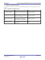
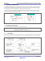
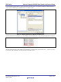
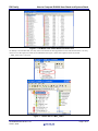
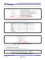
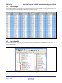
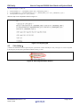
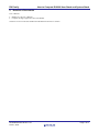
APPLICATION NOTE
RX Family
How to Compute RI600/4 User Stack and System Stack
R20AN0093ES0100
Rev.1.00
Oct 01, 2010
Introduction
Computing the required stack size is a critical step for embedded developers to avoid wasting any additional,
unnecessary memory and ensuring stack overflows does not occur. Deciding how much memory to allocate for the
stack has always been a trial and error process.
This document explains the method of computing the user stack and system stack for application written in RI600/4.
Target Device
Applicable MCU: RX Family
Contents
1.
Guide in using this Document ........................................................................................................... 2
2.
Introduction to RI600/4 Stack............................................................................................................ 3
3.
Computing User Stack Size .............................................................................................................. 3
4.
Computing System Stack Size.......................................................................................................... 6
5.
Reference Documents....................................................................................................................... 9
R20AN0093ES0100 Rev.1.00
Oct 01, 2010
Page 1 of 10
RX Family
1.
How to Compute RI600/4 User Stack and System Stack
Guide in using this Document
This document aims to equip users with the technique of determining the required user/task stack and system stack for
RI600/4.
Table 1
Explanation of Document Topics
Topic
Objective
Introduction to RI600/4
Explanation of user and system stack Knowledge in RI600/4
Computing User Stack Size
Explains methods of computing user
Knowledge in RI600/4
stack size to be allocated
Computing System Stack
Size
Explains methods of computing
system stack size to be allocated
Reference Documents
Listing of documents that equip users
None
with knowledge in the pre-requisite
requirements
R20AN0093ES0100 Rev.1.00
Oct 01, 2010
Pre-requisite
Knowledge in RI600/4
Page 2 of 10
RX Family
2.
How to Compute RI600/4 User Stack and System Stack
Introduction to RI600/4 Stack
In a program with RI600/4, there are two types of stacks defined: user stack and system stack. User stacks are allocated
for each individual task defined in the configuration file as shown in Figure 1. The size of user stack for each task is
also specified in the configuration file. System stack refers to the memory allocated for the kernel and various handlers.
The size of the system stack is also defined in the configuration file shown in Figure 1.
Caution will need to be exercised when allocating the sizes of the user stack and system stack. Allocating too much
memory will result in wasting of memory. Allocating too less will result in stack overflows, which can corrupt other
memory areas and typically trigger a program crash.
Figure 1 Setting User Stack and System Stack
3.
Computing User Stack Size
User stack size of each task is calculated based on the following expression.
Figure 2 Formulae for User Stack Size Computation
3.1
Calculating α
α denotes the size consumed by task entry function. This size can be computed using Call Walker. To measure the stack
size of α using Call Walker, either a stack information file (*.sni) or profile information file (*.pro) is required (Figure
3).
Figure 3 Linkage of each File in Call Walker
R20AN0093ES0100 Rev.1.00
Oct 01, 2010
Page 3 of 10
RX Family
How to Compute RI600/4 User Stack and System Stack
For the optimizing linkage editor to generate the stack information file, it is required to enable the “Stack information
output” option in HEW. Figure 4 illustrates how to select the option.
Figure 4 Enabling Generation of Stack Information File
Upon the compilation of the project, its corresponding stack information file (*.sni) will be generated shown in Figure 5.
Figure 5 Stack Information File
The stack information file is then loaded into Call Walker by choosing [File]->[Import Stack File…]. Figure 6 provides
a screenshot of the Call Walker with the loaded stack information file.
R20AN0093ES0100 Rev.1.00
Oct 01, 2010
Page 4 of 10
RX Family
How to Compute RI600/4 User Stack and System Stack
Figure 6 Call Walker with loaded Stack Information File
To identify α of individual task, user may refer to the numerical value append next to the task function name. User may
choose to view the required or used size of individual task. Figure 7 shows the required α stack size of task
“_Main_Task1 (72)” is 72 bytes.
Figure 7 α Stack Size of “Main_Task1”
R20AN0093ES0100 Rev.1.00
Oct 01, 2010
Page 5 of 10
RX Family
3.2
How to Compute RI600/4 User Stack and System Stack
Calculating β
β defines the task context size. The size of β is dependent on the system.context defined in the configuration file (Figure
8).
Figure 8 Defining β in Configuration File
User has eight options to choose from for the system.context entry. And each option will represent a different value of β.
Figure 9 shows the respective options and its corresponding task context size.
Figure 9 System.context and corresponding Task Context Size
Figure 10 shows the definition of task context size to be 80 bytes.
Figure 10 Example of a System.context Definition
The user stack size for task “Main_Task1” can therefore be computed at 152 bytes (72+80). Take note 152 bytes is the
minimum size that will be used by task “Main_Task1”.
4.
Computing System Stack Size
The system stack size can be computed based on the following expression.
Figure 11 Formulae for System Stack Size Computation
R20AN0093ES0100 Rev.1.00
Oct 01, 2010
Page 6 of 10
RX Family
4.1
How to Compute RI600/4 User Stack and System Stack
Calculating α
α denotes the maximum size among the service calls used. Figure 12 provides a sample table listing of the system stack
size for respective service call. The value α depends on the kernel version.
Figure 12 System Stack Size of RI600/4 Service Calls
4.2
Calculating Σβi
Σβi defines the total size consumed by the interrupts and system clock handlers across the different priority levels. For
multiple interrupts in the same priority level, the maximum size among the handlers is chosen. Below depicts a scenario
on how to calculate Σβi.
Figure 13 A Scenario of Computing System Stack
R20AN0093ES0100 Rev.1.00
Oct 01, 2010
Page 7 of 10
RX Family
How to Compute RI600/4 User Stack and System Stack
As shown in Figure 13, there are
• 2 alarm handlers (i.e. “_AlarmFlash_Alm2” and “_AlarmSetup_Alm1”)
• 3 cyclic handlers (i.e. “_StopWatchCount_Cyc3”, “_WatchUpdate_Cyc1” and “_LEDFlicker_Cyc4”)
• 1 OS-dependent interrupt (i.e. “_SW1_inh72”)
Therefore, Σβi can be computed as shown in Figure 14.
Figure 14 Computing Σβi
4.3
Calculating γ
γ denotes the summation of size required by the system down routine and 40bytes. The γ for Figure 15 can be computed
to be 44 bytes (4+40). If no system down routine is used, γ is zero.
Figure 15 Size of System Down Routine
R20AN0093ES0100 Rev.1.00
Oct 01, 2010
Page 8 of 10
RX Family
5.
How to Compute RI600/4 User Stack and System Stack
Reference Documents
User’s Manual
• RI600/4 V.1.00 User’s Manual
• Compiler Package Application Note Call Walker
The latest version can be downloaded from the Renesas Electronics website
R20AN0093ES0100 Rev.1.00
Oct 01, 2010
Page 9 of 10
RX Family
How to Compute RI600/4 User Stack and System Stack
Website and Support
Renesas Electronics Website
•
http://www.renesas.com/
Inquiries
•
http://www.renesas.com/inquiry
All trademarks and registered trademarks are the property of their respective owners.
R20AN0093ES0100 Rev.1.00
Oct 01, 2010
Page 10 of 10
Revision Record
Rev.
1.00
Date
Oct.01.10
Description
Page
Summary
—
First edition issued
A-1
General Precautions in the Handling of MPU/MCU Products
The following usage notes are applicable to all MPU/MCU products from Renesas. For detailed usage notes on the
products covered by this document, refer to the relevant sections of the document as well as any technical updates that
have been issued for the products.
1. Handling of Unused Pins
Handle unused pins in accord with the directions given under Handling of Unused Pins in the manual.
⎯ The input pins of CMOS products are generally in the high-impedance state. In operation with an
unused pin in the open-circuit state, extra electromagnetic noise is induced in the vicinity of LSI, an
associated shoot-through current flows internally, and malfunctions occur due to the false
recognition of the pin state as an input signal become possible. Unused pins should be handled as
described under Handling of Unused Pins in the manual.
2. Processing at Power-on
The state of the product is undefined at the moment when power is supplied.
⎯ The states of internal circuits in the LSI are indeterminate and the states of register settings and
pins are undefined at the moment when power is supplied.
In a finished product where the reset signal is applied to the external reset pin, the states of pins
are not guaranteed from the moment when power is supplied until the reset process is completed.
In a similar way, the states of pins in a product that is reset by an on-chip power-on reset function
are not guaranteed from the moment when power is supplied until the power reaches the level at
which resetting has been specified.
3. Prohibition of Access to Reserved Addresses
Access to reserved addresses is prohibited.
⎯ The reserved addresses are provided for the possible future expansion of functions. Do not access
these addresses; the correct operation of LSI is not guaranteed if they are accessed.
4. Clock Signals
After applying a reset, only release the reset line after the operating clock signal has become stable.
When switching the clock signal during program execution, wait until the target clock signal has
stabilized.
⎯ When the clock signal is generated with an external resonator (or from an external oscillator)
during a reset, ensure that the reset line is only released after full stabilization of the clock signal.
Moreover, when switching to a clock signal produced with an external resonator (or by an external
oscillator) while program execution is in progress, wait until the target clock signal is stable.
5. Differences between Products
Before changing from one product to another, i.e. to a product with a different part number, confirm
that the change will not lead to problems.
⎯ The characteristics of an MPU or MCU in the same group but having a different part number may
differ in terms of the internal memory capacity, layout pattern, and other factors, which can affect
the ranges of electrical characteristics, such as characteristic values, operating margins, immunity
to noise, and amount of radiated noise. When changing to a product with a different part number,
implement a system-evaluation test for the given product.
Notice
1.
All information included in this document is current as of the date this document is issued. Such information, however, is subject to change without any prior notice. Before purchasing or using any Renesas
Electronics products listed herein, please confirm the latest product information with a Renesas Electronics sales office. Also, please pay regular and careful attention to additional and different information to
be disclosed by Renesas Electronics such as that disclosed through our website.
2.
Renesas Electronics does not assume any liability for infringement of patents, copyrights, or other intellectual property rights of third parties by or arising from the use of Renesas Electronics products or
technical information described in this document. No license, express, implied or otherwise, is granted hereby under any patents, copyrights or other intellectual property rights of Renesas Electronics or
others.
3.
You should not alter, modify, copy, or otherwise misappropriate any Renesas Electronics product, whether in whole or in part.
4.
Descriptions of circuits, software and other related information in this document are provided only to illustrate the operation of semiconductor products and application examples. You are fully responsible for
the incorporation of these circuits, software, and information in the design of your equipment. Renesas Electronics assumes no responsibility for any losses incurred by you or third parties arising from the
use of these circuits, software, or information.
5.
When exporting the products or technology described in this document, you should comply with the applicable export control laws and regulations and follow the procedures required by such laws and
regulations. You should not use Renesas Electronics products or the technology described in this document for any purpose relating to military applications or use by the military, including but not limited to
the development of weapons of mass destruction. Renesas Electronics products and technology may not be used for or incorporated into any products or systems whose manufacture, use, or sale is
prohibited under any applicable domestic or foreign laws or regulations.
6.
Renesas Electronics has used reasonable care in preparing the information included in this document, but Renesas Electronics does not warrant that such information is error free. Renesas Electronics
7.
Renesas Electronics products are classified according to the following three quality grades: "Standard", "High Quality", and "Specific". The recommended applications for each Renesas Electronics product
assumes no liability whatsoever for any damages incurred by you resulting from errors in or omissions from the information included herein.
depends on the product's quality grade, as indicated below. You must check the quality grade of each Renesas Electronics product before using it in a particular application. You may not use any Renesas
Electronics product for any application categorized as "Specific" without the prior written consent of Renesas Electronics. Further, you may not use any Renesas Electronics product for any application for
which it is not intended without the prior written consent of Renesas Electronics. Renesas Electronics shall not be in any way liable for any damages or losses incurred by you or third parties arising from the
use of any Renesas Electronics product for an application categorized as "Specific" or for which the product is not intended where you have failed to obtain the prior written consent of Renesas Electronics.
The quality grade of each Renesas Electronics product is "Standard" unless otherwise expressly specified in a Renesas Electronics data sheets or data books, etc.
"Standard":
Computers; office equipment; communications equipment; test and measurement equipment; audio and visual equipment; home electronic appliances; machine tools;
personal electronic equipment; and industrial robots.
"High Quality": Transportation equipment (automobiles, trains, ships, etc.); traffic control systems; anti-disaster systems; anti-crime systems; safety equipment; and medical equipment not specifically
designed for life support.
"Specific":
Aircraft; aerospace equipment; submersible repeaters; nuclear reactor control systems; medical equipment or systems for life support (e.g. artificial life support devices or systems), surgical
implantations, or healthcare intervention (e.g. excision, etc.), and any other applications or purposes that pose a direct threat to human life.
8.
You should use the Renesas Electronics products described in this document within the range specified by Renesas Electronics, especially with respect to the maximum rating, operating supply voltage
range, movement power voltage range, heat radiation characteristics, installation and other product characteristics. Renesas Electronics shall have no liability for malfunctions or damages arising out of the
use of Renesas Electronics products beyond such specified ranges.
9.
Although Renesas Electronics endeavors to improve the quality and reliability of its products, semiconductor products have specific characteristics such as the occurrence of failure at a certain rate and
malfunctions under certain use conditions. Further, Renesas Electronics products are not subject to radiation resistance design. Please be sure to implement safety measures to guard them against the
possibility of physical injury, and injury or damage caused by fire in the event of the failure of a Renesas Electronics product, such as safety design for hardware and software including but not limited to
redundancy, fire control and malfunction prevention, appropriate treatment for aging degradation or any other appropriate measures. Because the evaluation of microcomputer software alone is very difficult,
please evaluate the safety of the final products or system manufactured by you.
10. Please contact a Renesas Electronics sales office for details as to environmental matters such as the environmental compatibility of each Renesas Electronics product. Please use Renesas Electronics
products in compliance with all applicable laws and regulations that regulate the inclusion or use of controlled substances, including without limitation, the EU RoHS Directive. Renesas Electronics assumes
no liability for damages or losses occurring as a result of your noncompliance with applicable laws and regulations.
11. This document may not be reproduced or duplicated, in any form, in whole or in part, without prior written consent of Renesas Electronics.
12. Please contact a Renesas Electronics sales office if you have any questions regarding the information contained in this document or Renesas Electronics products, or if you have any other inquiries.
(Note 1)
(Note 2)
"Renesas Electronics" as used in this document means Renesas Electronics Corporation and also includes its majority-owned subsidiaries.
"Renesas Electronics product(s)" means any product developed or manufactured by or for Renesas Electronics.
http://www.renesas.com
SALES OFFICES
Refer to "http://www.renesas.com/" for the latest and detailed information.
Renesas Electronics America Inc.
2880 Scott Boulevard Santa Clara, CA 95050-2554, U.S.A.
Tel: +1-408-588-6000, Fax: +1-408-588-6130
Renesas Electronics Canada Limited
1101 Nicholson Road, Newmarket, Ontario L3Y 9C3, Canada
Tel: +1-905-898-5441, Fax: +1-905-898-3220
Renesas Electronics Europe Limited
Dukes Meadow, Millboard Road, Bourne End, Buckinghamshire, SL8 5FH, U.K
Tel: +44-1628-585-100, Fax: +44-1628-585-900
Renesas Electronics Europe GmbH
Arcadiastrasse 10, 40472 Düsseldorf, Germany
Tel: +49-211-6503-0, Fax: +49-211-6503-1327
Renesas Electronics (China) Co., Ltd.
7th Floor, Quantum Plaza, No.27 ZhiChunLu Haidian District, Beijing 100083, P.R.China
Tel: +86-10-8235-1155, Fax: +86-10-8235-7679
Renesas Electronics (Shanghai) Co., Ltd.
Unit 204, 205, AZIA Center, No.1233 Lujiazui Ring Rd., Pudong District, Shanghai 200120, China
Tel: +86-21-5877-1818, Fax: +86-21-6887-7858 / -7898
Renesas Electronics Hong Kong Limited
Unit 1601-1613, 16/F., Tower 2, Grand Century Place, 193 Prince Edward Road West, Mongkok, Kowloon, Hong Kong
Tel: +852-2886-9318, Fax: +852 2886-9022/9044
Renesas Electronics Taiwan Co., Ltd.
7F, No. 363 Fu Shing North Road Taipei, Taiwan, R.O.C.
Tel: +886-2-8175-9600, Fax: +886 2-8175-9670
Renesas Electronics Singapore Pte. Ltd.
1 harbourFront Avenue, #06-10, keppel Bay Tower, Singapore 098632
Tel: +65-6213-0200, Fax: +65-6278-8001
Renesas Electronics Malaysia Sdn.Bhd.
Unit 906, Block B, Menara Amcorp, Amcorp Trade Centre, No. 18, Jln Persiaran Barat, 46050 Petaling Jaya, Selangor Darul Ehsan, Malaysia
Tel: +60-3-7955-9390, Fax: +60-3-7955-9510
Renesas Electronics Korea Co., Ltd.
11F., Samik Lavied' or Bldg., 720-2 Yeoksam-Dong, Kangnam-Ku, Seoul 135-080, Korea
Tel: +82-2-558-3737, Fax: +82-2-558-5141
© 2010 Renesas Electronics Corporation. All rights reserved.
Colophon 1.0