1
MIPS
Verified
MIPS32® 24Kc™ Processor Core Datasheet
™
December 19, 2008
The MIPS32® 24Kc™ core from MIPS Technologies is a high-performance, low-power, 32-bit MIPS RISC core designed for
custom system-on-silicon applications. The core is designed for semiconductor manufacturing companies, ASIC developers,
and system OEMs who want to rapidly integrate their own custom logic and peripherals with a high-performance RISC
processor. Fully synthesizable and highly portable across processes, it can be easily integrated into full system-on-silicon
designs, allowing developers to focus their attention on end-user products.
The 24Kc core implements the MIPS32 Release 2 Architecture in an 8-stage pipeline. It includes support for the MIPS16e™
application specific extension and the 32-bit privileged resource architecture. This standard architecture allows support by a
wide range of industry-standard tools and development systems.
To maintain high pipeline utilization, dynamic branch prediction is included in the form of a Branch History Table and a Return
Prediction Stack. The Memory Management Unit (MMU) contains 4-entry instruction and 8-entry data Translation Lookaside
Buffers (ITLB/DTLB) and a configurable 16/32/64 dual-entry joint TLB (JTLB) with variable page sizes. Alternatively, for
applications not requiring address mapping or protection, the TLBs can be replaced with a simple Fixed Mapping mechanism.
The synthesizable 24Kc core includes a high performance Multiply/Divide Unit (MDU). The MDU is fully pipelined to support
a single cycle repeat rate for 32x32 MAC instructions, which enables multiply-intensive algorithms to be performed efficiently.
Further, in the 24Kc Pro™ Core, the optional CorExtend block can utilize the HI/LO registers in the MDU block. The
CorExtend block allows specialized functions to be efficiently implemented.
Instruction and data level-one caches are configurable at 0, 8, 16, 32, or 64 KB in size. Each cache is organized as 4-way set
associative. Data cache misses are non-blocking and up to 8 may be outstanding. Two instruction cache misses can be
outstanding. Both caches are virtually indexed and physically tagged to allow them to be accessed in the same cycle that the
address is translated. To achieve high frequencies while using commercially available SRAM generators, the cache access is
spread across two pipeline stages, leaving nearly an entire cycle for the SRAM access.
The Bus Interface Unit implements the Open Core Protocol (OCP) which has been developed to address the needs of SOC
designers. This implementation features 64-bit read and write data buses to efficiently transfer data to and from the L1 caches.
The BIU also supports a variety of core/bus clock ratios to give greater flexibility for system design implementations.
The core features optional support for external interfaces to a coprocessor block and scratchpad RAMs. Separate instruction and
data scratchpads are supported, with reference designs featuring external OCP interfaces for system access to the arrays.
An Enhanced JTAG (EJTAG) compliant block allows for software debugging of the processor and includes a TAP controller
as well as optional instruction and data virtual address/value breakpoints. Additionally, real-time tracing of instruction program
counter, data address and data values can be supported.
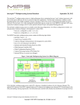
Figure 1 shows a block diagram of the 24Kc core.
MIPS32® 24Kc™ Processor Core Datasheet, Revision 04.00
Copyright © 2004-2008 MIPS Technologies Inc. All rights reserved.
MD00346
Figure 1
ISPRAM
DMA OCP I/F
Instruction
Scratchpad
RAM
EJTAG
PDTrace
TAP
Off/On-Chip
Trace I/F
Off-Chip
Debug I/F
CorExtend
Fetch Unit
8 entry instruction
buffer
512 entry BHT
4 entry RPS
MDU
Execution
Unit (RF/
ALU/Shift)
User-defined
COP2 block
I-cache
0/8/16/32/64KB
4 way set associative
MMU
16/32/64 entry
JTLB
or FMT
BIU
4 entry
merging write
buffer, 10
outstanding
reads
OCP Interface
On-Chip Bus(es)
User-defined
CorExtend
block
24Kc™ Core Block Diagram
CP2
System
Coprocessor
D-cache
0/8/16/32/64KB
4 way set associative
Power
Mgmt
Fixed/Required
Data
Scratchpad
RAM
DSPRAM DMA
OCP Interface
Non blocking
Load/Store Unit
8 outstanding misses
Optional
24Kc™ Core Features
• 8-stage pipeline
• 64-bit data paths to caches and external interface
• 32-bit address paths
2
MIPS32® 24Kc™ Processor Core Datasheet, Revision 04.00
Copyright © 2004-2008 MIPS Technologies Inc. All rights reserved.
• MIPS32 Release2 Instruction Set and Privileged
Resource Architecture
• MIPS16e™ Code Compression
• Programmable Memory Management Unit
–
–
–
–
–
–
–
–
–
–
–
–
–
16/32/64 dual-entry JTLB with variable page sizes
4-entry ITLB
8-entry DTLB
Optional simple Fixed Mapping Translation (FMT)
mechanism
Individually configurable instruction and data caches
sizes of 0/8/16/32/64 KB
4-Way Set Associative
Up to 8 outstanding load misses
Write-back and write-through support
32-byte cache line size
Virtually indexed, physically tagged
Cache line locking support
Non-blocking prefetches
Optional parity support
• Scratchpad RAM support
–
–
–
–
–
Separate RAMs for instruction and data
Independent of cache configuration
Maximum size of 1MB each
Interface allows back-stalling the core
Reference designs available featuring two 64 bit
OCP interfaces for external DMA
• Bus Interface
– OCP 2.1 compliant
– OCP interface with 32-bit address and 64-bit data
–
Flexible core:bus clock ratio support
– Burst size of four 64-bit beats
– 4 entry write buffer
– “Simple” byte enable mode allows easier bridging to
other bus standards
– Extensions for front-side L2 cache
–
–
–
–
Maintains full MIPS32 compatibility
Supported by industry standard development tools
Single or multi-cycle instructions
Includes access to HI and LO registers
• Coprocessor 2 interface
– 64 bit interface to a user designed coprocessor
• Power Control
–
–
–
–
Minimum frequency: 0 MHz
Power-down mode (triggered by WAIT instruction)
Support for software-controlled clock divider
Support for extensive use of local gated clocks
• EJTAG Debug
– Support for single stepping
– Virtual instruction and data address/value
breakpoints
– TAP controller is chainable for multi-CPU debug
– Cross-CPU breakpoint support
• MIPS Trace
– PC, data address and data value tracing w/ trace
compression
– Support for on-chip and off-chip trace memory
– PDTrace version 4.1 compliant
• Testability
– Full scan design achieves test coverage in excess of
99% (dependent on library and configuration
options)
– Optional memory BIST for internal SRAM arrays
Architecture Overview
The 24Kc core contains a variety of blocks some of which are
always present, while others are optional.
The required blocks are as follows:
• Fetch Unit
• Multiply/Divide Unit
– Maximum issue rate of one 32x32 multiply per
clock
– 5 cycle multiply latency
– Early-in iterative divide. Minimum 12 and
maximum 38 clock latency (dividend (rs) sign
extension-dependent)
• CorExtend™ User Defined Instruction Set Extensions
(available in 24Kc Pro™ core)
– Separately licensed; a core with this feature is
known as the 24Kc Pro™ core
– Allows user to define and add instructions to the
CPU at build time
• Execution Unit
• MIPS16e recode
• System Control Coprocessor (CP0)
• Memory Management Unit (MMU)
• Cache Controllers
• Bus Interface Unit (BIU)
• Power Management
Optional blocks include:
• CorExtend™ User Defined Instruction (UDI) support
• Enhanced JTAG (EJTAG) breakpoints
MIPS32® 24Kc™ Processor Core Datasheet, Revision 04.00
Copyright © 2004-2008 MIPS Technologies Inc. All rights reserved.
3
• MIPS Trace (PDtrace™) support
• Instruction watch and EJTAG break compares done
• Instruction/Data scratchpad
IS - Instruction Fetch Second
• COP2 interface
• Detect I-cache hit
• Way select
Pipeline Flow
• MIPS32 Branch prediction
The 24Kc core implements an 8-stage pipeline. Three extra
fetch stages are conditionally added when executing
MIPS16e instructions. This pipeline allows the processor to
achieve a high frequency while maintaining reasonable area
and power numbers.
IR - Instruction Recode
• MIPS16e instruction recode
• MIPS16e branch prediction
IK - Instruction Kill
The 24Kc core pipeline consists of the following stages:
• MIPS16e instruction kill
• IF - Instruction Fetch First
IT - Instruction Fetch Third
• IS - Instruction Fetch Second
• Instruction Buffer
• IR - Instruction Recode (MIPS16e only)
• Branch target calculation
• IK - Instruction Kill (MIPS16e only)
• IT - Instruction Fetch Third (MIPS16e only)
RF - Register File Access
• RF - Register File access
• Register File access
• AG - Address Generation
• Instruction decoding/dispatch logic
• EX - Execute
• Bypass muxes
• MS - Memory Second
AG - Address Generation
• ER - Exception Resolution
• D-cache Address Generation
• WB - WriteBack
• Bypass muxes
The 24Kc core implements a bypass mechanism that allows
the result of an operation to be forwarded directly to the
instruction that needs it without having to write the result to
the register and then read it back.
Figure 2 shows a diagram of the 24Kc core pipeline.
EX - Execute/Memory Access
• Skewed ALU
• DTLB
• Start DCache access
• Branch Resolution
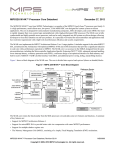
Figure 2 24Kc™ Core Pipeline
IF
IS
IR
IK
• Data watch and EJTAG break address compares
MS - Memory Access Second
IT
MIPS16e
32b code
• Complete DCache access
• DCache hit detection
• Way select mux
RF
AG
EX
MS
ER
WB
• Load align
• EJTAG break data value compare
IF Stage: Instruction Fetch First
ER- Exception Resolution
• I-cache tag/data arrays accessed
• Instruction completion
• Branch History Table accessed
• Register file write setup
• ITLB address translation performed
• Exception processing
4
MIPS32® 24Kc™ Processor Core Datasheet, Revision 04.00
Copyright © 2004-2008 MIPS Technologies Inc. All rights reserved.
WB - Writeback
The execution unit includes:
• Register file writeback occurs on rising edge of this cycle
• 32-bit adder used for calculating the data address
• Logic for verifying branch prediction
24Kc™ Core Logic Blocks
• Load aligner
The 24Kc core consists of the following logic blocks, shown
in Figure 1. These logic blocks are defined in the following
subsections:
• Bypass multiplexers used to avoid stalls when executing
instructions streams where data producing instructions
are followed closely by consumers of their results
• Fetch Unit
• Leading Zero/One detect unit for implementing the CLZ
and CLO instructions
• Execution Unit
• MIPS16e support
• Arithmetic Logic Unit (ALU) for performing bitwise
logical operations
• System Control Coprocessor (CP0)
• Shifter & Store Aligner
• Memory Management Unit (MMU)
• Cache Controller
MIPS16e™ Application Specific Extension
• Bus Interface Unit (BIU)
The 24Kc core includes support for the MIPS16e ASE. This
ASE improves code density through the use of 16-bit
encoding of many MIPS32 instructions plus some MIPS16especific instructions. PC relative loads allow quick access to
constants. Save/Restore macro instructions provide for single
instruction stack frame setup/teardown for efficient
subroutine entry/exit.
• Power Management
Fetch Unit
The 24Kc core fetch unit is responsible for fetching
instructions and providing them to the rest of the pipeline, as
well as handling control transfer instructions (branches,
jumps, etc.). It calculates the address for each instruction
fetch and contains an instruction buffer that decouples the
fetching of instructions from their execution.
The fetch unit contains two structures for the dynamic
prediction of control transfer instructions. A 512-entry
Branch History Table (BHT) is used to predict the direction
of branch instructions. It uses a bimodal algorithm with two
bits of history information per entry. Also, a 4-entry Return
Prediction Stack (RPS) is a simple structure to hold the return
address from the most recent subroutine calls. The link
address is pushed onto the stack whenever a JAL, JALR, or
BGEZAL instruction is seen. Then that address is popped
when a JR instruction occurs.
Multiply/Divide Unit (MDU)
The 24Kc core includes a multiply/divide unit (MDU) that
contains a separate pipeline for integer multiply and divide
operations. This pipeline operates in parallel with the integer
unit pipeline and does not stall when the integer pipeline
stalls. This allows any long-running MDU operations to be
partially masked by system stalls and/or other integer unit
instructions.
The MDU consists of a pipelined 32x32 multiplier, result/
accumulation registers (HI and LO), a divide state machine,
and the necessary multiplexers and control logic.
The MDU supports execution of one multiply or multiply
accumulate operation every clock cycle.
Execution Unit
The 24Kc core execution unit implements a load/store
architecture with single-cycle ALU operations (logical, shift,
add, subtract) and an autonomous multiply/divide unit. The
24Kc core contains thirty-two 32-bit general-purpose
registers used for integer operations and address calculation.
Optionally, one or three additional register file shadow sets
(each containing thirty-two registers) can be added to
minimize context switching overhead during interrupt/
exception processing. The register file consists of two read
ports and one write port and is fully bypassed to minimize
operation latency in the pipeline.
Divide operations are implemented with a simple 1 bit per
clock iterative algorithm. An early-in detection checks the
sign extension of the dividend (rs) operand. If rs is 8 bits
wide, 23 iterations are skipped. For a 16-bit-wide rs, 15
iterations are skipped, and for a 24-bit-wide rs, 7 iterations
are skipped. Any attempt to issue a subsequent MDU
instruction while a divide is still active causes a pipeline stall
until the divide operation is completed.
Table 1 lists the latencies (number of cycles until a result is
available) and repeat rates (peak issue rate of cycles until the
operation can be reissued) for the 24Kc core multiply and
MIPS32® 24Kc™ Processor Core Datasheet, Revision 04.00
Copyright © 2004-2008 MIPS Technologies Inc. All rights reserved.
5
divide instructions. The approximate latency and repeat rates
are listed in terms of pipeline clocks. For a more detailed
discussion of latencies and repeat rates, refer to Chapter 2 of
the MIPS32 24K Processor Core Family Software User’s
Manual.
Table 1
24Kc™ Core Integer Multiply/Divide Unit
Latencies and Repeat Rates
Operand
Size
(mul rt)
(div rs)
Latency
Repeat
Rate
MULT/MULTU,
MADD/MADDU,
MSUB/MSUBU
32 bits
5
1
MUL
32 bits
5
11
8 bits
12/14
12/14
16 bits
20/22
20/22
24 bits
28/30
28/30
32 bits
36/38
36/38
Opcode
DIV/DIVU
1. If there is no data dependency, a MUL can be issued every
cycle.
The MIPS architecture defines that the result of a multiply or
divide operation be placed in the HI and LO registers. Using
the Move-From-HI (MFHI) and Move-From-LO (MFLO)
instructions, these values can be transferred to the generalpurpose register file.
In addition to the HI/LO targeted operations, the MIPS32
architecture also defines a multiply instruction, MUL, which
places the least significant results in the primary register file
instead of the HI/LO register pair.
Two other instructions, multiply-add (MADD) and multiplysubtract (MSUB), are used to perform the multiplyaccumulate and multiply-subtract operations. The MADD
instruction multiplies two numbers and then adds the product
to the current contents of the HI and LO registers. Similarly,
the MSUB instruction multiplies two operands and then
subtracts the product from the HI and LO registers. The
MADD and MSUB operations are commonly used in DSP
algorithms.
System Control Coprocessor (CP0)
In the MIPS architecture, CP0 is responsible for the virtualto-physical address translation and cache protocols, the
exception control system, the processor’s diagnostic
6
capability, the operating modes (kernel, user, supervisor, and
debug), and whether interrupts are enabled or disabled.
Configuration information, such as cache size and
associativity, presence of features like MIPS16e or floating
point unit, is also available by accessing the CP0 registers.
Coprocessor 0 also contains the logic for identifying and
managing exceptions. Exceptions can be caused by a variety
of sources, including boundary cases in data, external events,
or program errors.
Interrupt Handling
The 24Kc core includes support for six hardware interrupt
pins, two software interrupts, a timer interrupt, and a
performance counter interrupt. These interrupts can be used
in any of three interrupt modes, as defined by Release 2 of the
MIPS32 Architecture:
• Interrupt compatibility mode, which acts identically to
that in an implementation of Release 1 of the
Architecture.
• Vectored Interrupt (VI) mode, which adds the ability to
prioritize and vector interrupts to a handler dedicated to
that interrupt, and to assign a GPR shadow set for use
during interrupt processing. The presence of this mode is
denoted by the VInt bit in the Config3 register. This
mode is architecturally optional; but it is always present
on the 24Kc core, so the VInt bit will always read as a 1
for the 24Kc core.
• External Interrupt Controller (EIC) mode, which
redefines the way in which interrupts are handled to
provide full support for an external interrupt controller
handling prioritization and vectoring of interrupts. The
presence of this mode is denoted by the VEIC bit in the
Config3 register. Again, this mode is architecturally
optional. On the 24Kc core, the VEIC bit is set externally
by the static input, SI_EICPresent, to allow system logic
to indicate the presence of an external interrupt
controller.
The reset state of the processor is to interrupt compatibility
mode such that a processor supporting Release 2 of the
Architecture, like the 24Kc core, is fully compatible with
implementations of Release 1 of the Architecture.
VI or EIC interrupt modes can be combined with the optional
shadow registers to specify which shadow set should be used
upon entry to a particular vector. The shadow registers further
improve interrupt latency by avoiding the need to save
context when invoking an interrupt handler.
MIPS32® 24Kc™ Processor Core Datasheet, Revision 04.00
Copyright © 2004-2008 MIPS Technologies Inc. All rights reserved.
GPR Shadow Registers
Release 2 of the MIPS32 Architecture optionally removes the
need to save and restore GPRs on entry to high priority
interrupts or exceptions, and to provide specified processor
modes with the same capability. This is done by introducing
multiple copies of the GPRs, called shadow sets, and
allowing privileged software to associate a shadow set with
entry to kernel mode via an interrupt vector or exception. The
normal GPRs are logically considered shadow set zero.
The number of GPR shadow sets is a build-time option on the
24Kc core. Although Release 2 of the Architecture defines a
maximum of 16 shadow sets, the core allows one (the normal
GPRs), two, or four shadow sets. The highest number actually
implemented is indicated by the SRSCtlHSS field. If this field
is zero, only the normal GPRs are implemented.
Shadow sets are new copies of the GPRs that can be
substituted for the normal GPRs on entry to kernel mode via
an interrupt or exception. Once a shadow set is bound to a
kernel mode entry condition, reference to GPRs work exactly
as one would expect, but they are redirected to registers that
are dedicated to that condition. Privileged software may need
to reference all GPRs in the register file, even specific
shadow registers that are not visible in the current mode. The
RDPGPR and WRPGPR instructions are used for this
purpose. The CSS field of the SRSCtl register provides the
number of the current shadow register set, and the PSS field
of the SRSCtl register provides the number of the previous
shadow register set (that which was current before the last
exception or interrupt occurred).
If the processor is operating in VI interrupt mode, binding of
a vectored interrupt to a shadow set is done by writing to the
SRSMap register. If the processor is operating in EIC
interrupt mode, the binding of the interrupt to a specific
shadow set is provided by the external interrupt controller,
and is configured in an implementation-dependent way.
Binding of an exception or non-vectored interrupt to a
shadow set is done by writing to the ESS field of the SRSCtl
register. When an exception or interrupt occurs, the value of
SRSCtl CSS is copied to SRSCtlPSS, and SRSCtlCSS is set
to the value taken from the appropriate source. On an ERET,
the value of SRSCtlPSS is copied back into SRSCtlCSS to
restore the shadow set of the mode to which control returns.
Modes of Operation
The 24Kc core supports four modes of operation: user mode,
supervisor mode, kernel mode, and debug mode. User mode
is most often used for application programs. Supervisor mode
gives an intermediate privilege level with access to the ksseg
address space. Supervisor mode is not supported with the
fixed mapping MMU. Kernel mode is typically used for
handling exceptions and operating system kernel functions,
including CP0 management and I/O device accesses. An
additional Debug mode is used during system bring-up and
software development. Refer to "EJTAG Debug Support" on
page 14 for more information on debug mode.
Memory Management Unit (MMU)
The 24Kc core contains a configurable Memory Management
Unit (MMU) that is primarily responsible for converting
virtual addresses to physical addresses and providing
attribute information for different segments of memory.
Two types of MMUs are possible on the 24Kc core, selectable
when the core is synthesized. Software can identify the type
of MMU present by querying the MT field of the Config
register.
1. Translation Lookaside Buffer (TLB)-style MMU. The
basic TLB functionality is specified by the MIPS32
Privileged Resource Architecture (PRA). A TLB provides mapping and protection capability with per-page
granularity. The 24Kc implementation allows a wide
range of page sizes to be present simultaneously.
2. Fixed Mapping Translation (FMT)-style MMU. The
FMT is much simpler and smaller than the TLB-style
MMU, and is a good choice when the full protection and
flexibility of the TLB is not needed.
Translation Lookaside Buffer (TLB)
The basic TLB functionality is specified by the MIPS32
Privileged Resource Architecture. A TLB provides mapping
and protection capability with per-page granularity. The
24Kc implementation allows a wide range of page sizes to be
present simultaneously.
The TLB contains a fully associative Joint TLB (JTLB). To
enable higher clock speeds, two smaller micro-TLBs are also
implemented: the Instruction Micro TLB (ITLB) and the
Data Micro TLB (DTLB). When an instruction or data
address is calculated, the virtual address is compared to the
contents of the appropriate micro TLB (uTLB). If the address
is not found in the uTLB, the JTLB is accessed. If the entry is
found in the JTLB, that entry is then written into the uTLB. If
the address is not found in the JTLB, a TLB exception is
taken.
Figure 3 shows how the ITLB, DTLB, and JTLB are
implemented in the 24Kc core.
MIPS32® 24Kc™ Processor Core Datasheet, Revision 04.00
Copyright © 2004-2008 MIPS Technologies Inc. All rights reserved.
7
Figure 3 Address Translation During a Cache
Access.
Virtual Address
Instruction
Address
Calculator
ITLB
IVA
Instruction
Cache
Tag RAM
Comparator
Instruction
Hit/Miss
Entry
The ITLB is managed by hardware and is transparent to
software. The larger JTLB is used as a backing structure for
the ITLB. If a fetch address cannot be translated by the ITLB,
the JTLB is used to attempt to translate it in the following
clock cycle, or when available. If successful, the translation
information is copied into the ITLB for future use. There is a
minimum two cycle ITLB miss penalty.
Data TLB (DTLB)
JTLB
DVA
Data
Address
Calculator
Data
Hit/Miss
Entry
DTLB
Virtual Address
Comparator
Data
Cache
TagRAM
Joint TLB (JTLB)
The 24Kc core implements a fully associative JTLB
containing 16, 32, or 64-dual-entries mapping up to 128
virtual pages to their corresponding physical addresses. The
purpose of the TLB is to translate virtual addresses and their
corresponding ASIDs into a physical memory address. The
translation is performed by comparing the upper bits of the
virtual address (along with the ASID) against each of the
entries in the tag portion of the joint TLB structure.
The JTLB is organized as pairs of even and odd entries
containing pages that range in size from 4 KB to 256 MB, in
factors of four, into the 4 GB physical address space. The
JTLB is organized in page pairs to minimize the overall size.
Each tag entry corresponds to two data entries: an even page
entry and an odd page entry. The highest order virtual address
bit not participating in the tag comparison is used to
determine which of the data entries is used. Since page size
can vary on a page-pair basis, the determination of which
address bits participate in the comparison and which bit is
used to make the even-odd determination is decided
dynamically during the TLB look-up.
Instruction TLB (ITLB)
The ITLB is a small 4-entry, fully associative TLB dedicated
to performing translations for the instruction stream. The
ITLB only maps 4 KB or 1 MB pages/subpages. For 4 KB or
1 MB pages, the entire page is mapped in the ITLB. If the
main TLB page size is between 4 KB and 1 MB, only the
current 4 KB subpage is mapped. Similarly, for page sizes
larger than 1 MB, the current 1 MB subpage is mapped.
8
The DTLB is a small 8-entry, fully associative TLB dedicated
to performing translations for loads and stores. Similar to the
ITLB, the DTLB only maps either 4 KB or 1 MB pages/
subpages.
The DTLB is managed by hardware and is transparent to
software. The larger JTLB is used as a backing structure for
the DTLB. If a load/store address cannot be translated by the
DTLB, a lookup is done in the JTLB. If the JTLB translation
is successful, the translation information is copied into the
DTLB for future use. The DTLB miss penalty is also two
cycles.
Fixed Mapping Translation (FMT)
The FMT is much simpler and smaller than the TLB-style
MMU, and is a good choice when the full protection and
flexibility of the TLB is not needed. Like a TLB, the FMT
performs virtual-to-physical address translation and provides
attributes for the different segments. Those segments that are
unmapped in a TLB implementation (kseg0 and kseg1) are
handled identically by the FMT.
Instruction Cache
The instruction cache is an on-chip memory block of 0/8/16/
32/64 KB, with 4-way associativity. Because the instruction
cache is virtually indexed, the virtual-to-physical address
translation occurs in parallel with the cache access rather than
having to wait for the physical address translation. A tag entry
holds 20 bits of physical address, a valid bit, a lock bit, and an
optional parity bit per way. The instruction data entry holds
two instructions (64 bits) per way, as well as 6 bits of predecode information to speed the decode of branch and jump
instructions, and 9 optional parity bits (one per data byte plus
one more for the pre-decode information). The LRU
replacement bits (6b) are stored in a separate array.
The instruction cache block also contains and manages the
instruction line fill buffer. Besides accumulating data to be
written to the cache, instruction fetches that reference data in
the line fill buffer are serviced either by a bypass of that data,
or data coming from the external interface. The instruction
cache control logic controls the bypass function.
MIPS32® 24Kc™ Processor Core Datasheet, Revision 04.00
Copyright © 2004-2008 MIPS Technologies Inc. All rights reserved.
The 24Kc core supports instruction-cache locking. Cache
locking allows critical code or data segments to be locked into
the cache on a “per-line” basis, enabling the system
programmer to maximize the efficiency of the system cache.
Table 2
24Kc™ Core Instruction and Data
Cache Attributes
Parameter
Instruction
Data
Size
0, 8, 16, 32, or 64
KB*
0, 8, 16, 32, or
64 KB
The cache-locking function is always available on all
instruction-cache entries. Entries can then be marked as
locked or unlocked on a per entry basis using the CACHE
instruction.
Organization
4 way set associative
4 way set associative
Data Cache
Line Size
32 Bytes*
32 Bytes
The data cache is an on-chip memory block of 0/8/16/32/64
KB, with 4-way associativity. Since the data cache is virtually
indexed, the virtual-to-physical address translation occurs in
parallel with the cache access. A tag entry holds 20 bits of
physical address, a valid bit, a lock bit, and an optional parity
bit per way. The data entry holds 64 bits of data per way, with
optional parity per byte. There is an additional array holding
dirty bits and LRU replacement algorithm bits (6b LRU, 4b
dirty, and optionally 4b dirty parity).
Read Unit
64 bits*
64 bits
Write Policies
N/A
write-through
without write
allocate,
write-back with
write allocate
Miss restart after
transfer of
miss word
miss word
Cache Locking
per line
per line
Using 4KB pages in the TLB and 32 or 64KB cache sizes it
is possible to get virtual aliasing. A single physical address
can exist in multiple cache locations if it was accessed via
different virtual addresses. For both 32KB and 64KB data
cache options, there is an implementation option to eliminate
virtual aliasing. If this option is not selected, software must
take care of any aliasing issues by using a page coloring
scheme or some other mechanism.
In addition to instruction-cache locking, the 24Kc core also
supports a data-cache locking mechanism identical to the
instruction cache. Critical data segments are locked into the
cache on a “per-line” basis. The locked contents can be
updated on a store hit, but will not be selected for replacement
on a cache miss.
The cache-locking function is always available on all data
cache entries. Entries can then be marked as locked or
unlocked on a per-entry basis using the CACHE instruction.
Cache Memory Configuration
The 24Kc core incorporates on-chip instruction and data
caches that are usually implemented from readily available
single-port synchronous SRAMs and accessed in two cycles:
one cycle for the actual SRAM read and another cycle for the
tag comparison, hit determination, and way selection. The
instruction and data caches each have their own 64-bit data
paths and can be accessed simultaneously. Table 2 lists the
24Kc core instruction and data cache attributes.
*Logical size of instruction cache. Cache physically contains some extra bits used for precoding the instruction
type.
Cache Protocols
The 24Kc core supports the following cache protocols:
• Uncached: Addresses in a memory area indicated as
uncached are not read from the cache. Stores to such
addresses are written directly to main memory, without
changing cache contents.
• Write-through, no write allocate: Loads and instruction
fetches first search the cache, reading main memory only
if the desired data does not reside in the cache. On data
store operations, the cache is first searched to see if the
target address is cache resident. If it is resident, the cache
contents are updated, and main memory is also written. If
the cache look-up misses, only main memory is written.
• Write-back, write allocate: Stores that miss in the cache
will cause a cache refill. Store data, however, is only
written to the cache. Caches lines that are written by
stores will be marked as dirty. If a dirty line is selected
for replacement, the cache line will be written back to
main memory.
MIPS32® 24Kc™ Processor Core Datasheet, Revision 04.00
Copyright © 2004-2008 MIPS Technologies Inc. All rights reserved.
9
• Uncached Accelerated: Like uncached, data is never
loaded into the cache. Store data can be gathered in a
write buffer before being sent out on the bus as a bursted
write. This is more efficient than sending out individual
writes as occurs in regular uncached mode.
OCP Interface
Table 3 shows the OCP Performance Report for the 24Kc
core. This table lists characteristics about the core and the
specific OCP functionality that is supported.
Bus Interface (BIU)
The Bus Interface Unit (BIU) controls the external interface
signals. The primary interface implements the Open Core
Protocol (OCP). Additionally, the BIU includes a write
buffer.
Table 3
OCP Performance Report
Core name
24Kc
Core Identity
TBD
Vendor Code
TBD
Core Code
0x93, visible in ProcessorID field of CP0 PrID register
Revision Code
Visible in Revision field of PrID register
Process dependent
No
Frequency range for this
core
Synthesizable, so varies based on process, libraries, and implementation
Area
Synthesizable, so varies based on process, libraries, and implementation
Power Estimate
Synthesizable, so varies based on process, libraries, and implementation
Special reset requirements
No
Number of Interfaces
1 OCP master, 2 OCP slave (DMA access for SPRAMs)
Interface Information:
• Name
OCPMasterInterface
• Type
Master
Master OCP Interface
10
Operations issued
RD, WR
Issue rate (per OCP cycle)
One per cycle, for all of the types listed above except for a non-standard RD (SYNC) which depends
on ack latency.
Maximum number of
operations outstanding
10 read operations. All writes are posted, so the OCP fabric determines the maximum number of
outstanding writes.
Burst support and effect on
issue rates
Fixed burst length of four 64b beats with single request per burst. Burst sequences of WRAP or XOR
supported.
High level flow control
None
Number of tags supported
and use of those tags
Total of 12 tags: 10 tags for outstanding RD’s, 1 tag for WR & 1 tag for SYNC
Connection ID and use of
connection information
None
Use of sideband signals
None
MIPS32® 24Kc™ Processor Core Datasheet, Revision 04.00
Copyright © 2004-2008 MIPS Technologies Inc. All rights reserved.
Table 3
OCP Performance Report (Continued)
1. MReqInfo handled in a user-defined way.
Implementation
restrictions
2. MAddrSpace is used (2 bits) to indicate L2/L3 access.
3. Core clock is synchronous but a multiple of the OCP clock. Strobe inputs to the core control input
and output registers to establish the core:bus clock ratio.
Interface Information:
• Name
OCPSlaveInterface
• Type
Slave
Slave OCP Interfaces (DMA interface to scratchpad)
Operations accepted
RD, WR
Issue rate (per OCP cycle)
One per cycle, for all of the types listed above except for a non-standard RD (SYNC) which is not
supported.
Maximum number of
operations outstanding
2 outstanding operations which includes both RD & WR.
Burst support
Burst access is not supported
High level flow control
Back pressure from slave on data and command accept. Slave assumes no back pressure from the
master.
Number of tags supported
and use of those tags
Total of 8 tags. Any tag number can be used for read and write operation.
Connection ID and use of
connection information
None
Use of sideband signals
None
Implementation
restrictions
The slave interface operates at the same clock ratio as that of the master OCP interface.
Write Buffer
Uncached Accelerated
The BIU contains a merging write buffer. The purpose of this
buffer is to store and combine write transactions before
issuing them to the external interface. The write buffer is
organized as four 32-byte buffers. Each buffer contains data
from a single 32-byte aligned block of memory.
For uncached accelerated references, the write buffer can
gather multiple writes together and then perform a bursted
write to increase the efficiency of the bus. Uncached
accelerated gathering is supported for word and double word
stores only.
Write Through
Gathering of uncached accelerated stores will start on cacheline aligned addresses, i.e. 32 byte aligned addresses. Once an
uncached accelerated store starts gathering, a gather buffer is
reserved for this store. All subsequent uncached accelerated
word or double word stores to the same 32B region will write
sequentially into this buffer, independent of the word address
associated with these latter stores. The uncached accelerated
buffer is tagged with the address of the first store. An
uncached accelerated store that does not merge and does not
go to an aligned address will be treated as a regular uncached
store.
When using the write-through cache policy, the write buffer
significantly reduces the number of write transactions on the
external interface and reduces the amount of stalling in the
core due to issuance of multiple writes in a short period of
time.
Write Back
The write buffer also holds eviction data for write-back lines.
The load-store unit opportunistically pulls dirty data from the
cache and sends it to the BIU. It is gathered in the write buffer
and sent out as a bursted write.
MIPS32® 24Kc™ Processor Core Datasheet, Revision 04.00
Copyright © 2004-2008 MIPS Technologies Inc. All rights reserved.
11
SimpleBE Mode
To aid in attaching the 24Kc core to structures which cannot
easily handle arbitrary byte enable patterns, there is a mode
that generates only “simple” byte enables. Only byte enables
representing naturally aligned byte, halfword, word, and
doubleword transactions will be generated.
The only case where a read can generate “non-simple” byte
enables is on an uncached tri-byte load (LWL/LWR). In
SimpleBE mode, such reads will be converted into a word
read on the external interface.
Writes with non-simple byte enable patterns can arise when a
sequence of stores is processed by the merging write buffer,
or from uncached tri-byte stores (SWL/SWR). In SimpleBE
mode, these stores will be broken into multiple write
transactions.
In debug mode, EJTAG can request that a ‘soft’ reset be
masked. This request is signalled via the EJ_SRstE pin.
When this pin is deasserted, the system can choose to block
some sources of soft reset. Hard resets, such as power-on
reset or a reset switch should not be blocked by this signal.
Power Management
The 24Kc core offers a number of power management
features, including low-power design, active power
management, and power-down modes of operation. The core
is a static design that supports slowing or halting the clocks,
which reduces system power consumption during idle
periods.
The 24Kc core provides two mechanisms for system-level
low power support:
• Register-controlled power management
• Instruction-controlled power management
Clocking
The core has 3 primary clock domains:
• Core domain - This is the main core clock domain,
controlled by the SI_ClkIn clock input.
• OCP domain - This domain controls the OCP bus
interface logic. This domain is synchronous to SI_ClkIn,
but can be run at a different frequency. The core does not
contain an explicit OCP input clock; all flops are actually
controlled by SI_ClkIn. Additional inputs control when
inputs should be sampled and outputs should be driven
• TAP domain - This is a low speed clock domain for the
EJTAG TAP controller, controlled by the EJ_TCK pin. It
is asynchronous to SI_ClkIn.
Hardware Reset
Unlike previous MIPS cores, a 24Kc core only has a single
reset input. Historically, cold reset was used to reset a PLL. In
synthesizable cores without a PLL, the two inputs were ORed
together internally and then treated identically (except for a
Status bit indicating which reset was seen). The 24Kc
interface has removed the second reset type and only includes
the SI_Reset pin.
Register-Controlled Power Management
The RP bit in the CP0 Status register provides a software
mechanism for placing the system into a low power state. The
state of the RP bit is available externally via the SI_RP signal.
The external agent then decides whether to place the device
in a low power mode, such as reducing the system clock
frequency.
Three additional bits, StatusEXL, StatusERL, and DebugDM
support the power management function by allowing the user
to change the power state if an exception or error occurs while
the 24Kc core is in a low power state. Depending on what
type of exception is taken, one of these three bits will be
asserted and reflected on the SI_EXL, SI_ERL, or
EJ_DebugM outputs. The external agent can look at these
signals and determine whether to leave the low power state to
service the exception.
The following 4 power-down signals are part of the system
interface and change state as the corresponding bits in the
CP0 registers are set or cleared:
• The SI_RP signal represents the state of the RP bit (27)
in the CP0 Status register.
The SI_Reset input is used to initialize critical hardware
state. It can be asserted either synchronously or
asynchronously to the core clock, SI_ClkIn, and will trigger a
Reset exception. The reset signal is active high, and must be
asserted for a minimum of 5 SI_ClkIn cycles. The falling edge
triggers the Reset exception. The reset signal must be asserted
at power-on or whenever hardware initialization of the core is
desired.
• The SI_EXL signal represents the state of the EXL bit (1)
in the CP0 Status register.
12
MIPS32® 24Kc™ Processor Core Datasheet, Revision 04.00
• The SI_ERL signal represents the state of the ERL bit (2)
in the CP0 Status register.
• The EJ_DebugM signal represents the state of the DM bit
(30) in the CP0 Debug register.
Copyright © 2004-2008 MIPS Technologies Inc. All rights reserved.
Instruction-Controlled Power Management
The second mechanism for invoking power-down mode is
through execution of the WAIT instruction. When the WAIT
instruction is executed, the internal clock is suspended;
however, the internal timer and some of the input pins
(SI_Int[5:0], SI_NMI, and SI_Reset) continue to run. Once the
CPU is in instruction-controlled power management mode,
any interrupt, NMI, or reset condition causes the CPU to exit
this mode and resume normal operation.
The coprocessor interface is extensible and standardized on
MIPS cores, allowing design reuse. The 24Kc core supports
a subset of the full coprocessor interface standard: single
issue, 64 bit in-order data transfers.
The coprocessor interface is designed to ease integration with
customer IP. The interface allows high-performance
communication between the core and coprocessor. There are
no late or critical timing signals on the interface.
Data Scratchpad RAM (DSPRAM)
The 24Kc core asserts the SI_Sleep signal, which is part of
the system interface, whenever the WAIT instruction is
executed. The assertion of SI_Sleep indicates that the clock
has stopped and the 24Kc core is waiting for an interrupt.
The 24Kc core can be configured to include an optional Data
scratchpad RAM independent of the data cache
configuration. A separate OCP slave interface allows a DMA
master to access the data scratchpad RAM.
Local clock gating
A majority of the power consumed by the 24Kc core is often
in the clock tree and clocking registers. The core has support
for extensive use of local gated-clocks. Power-conscious
implementors can use these gated clocks to significantly
reduce power consumption within the core.
CorExtend™ User Defined Instruction
Extensions
The optional CorExtend User Defined Instruction (UDI)
block enables the implementation of a small number of
application-specific instructions that are tightly coupled to
the core’s integer execution unit.
The interface to the CorExtend block is similar to the
Multiply-Divide Unit, allowing non-blocking, pipelined
multi-cycle operations. A portion of the hooks into the MDU
control logic and also allows the HI/LO accumulation
registers to be used by the CorExtend block.
CorExtend instructions may operate on a general-purpose
register, immediate data specified by the instruction word, or
local state stored within the UDI block. The destination may
be a general-purpose register, HI/LO, or local UDI state. The
operation may complete in one cycle or multiple cycles, if
desired.
Coprocessor 2 interface
The 24Kc core can be configured to have an interface for an
on-chip coprocessor. The interface allows the coprocessor to
be tightly coupled to the processor core, allowing high
performance solutions, like integrating a graphics accelerator
or custom DSP.
To demonstrate use of the scratchpad capability, MIPS
provides a default design that includes one contiguous 8 KB
RAM with cache-like access. A DSPRAM hit supersedes a
data cache hit. DSPRAM is indexed by virtual address. The
hit information is based on the physical address in the base
register. DSPRAM can be mapped to either cacheable or noncacheable address space. A sophisticated arbitration scheme
and instruction slip in the pipe prevents unnecessary stalls.
Only store instructions which are guaranteed to complete and
hit in the DSPRAM, arbitrate for the RAM. The DMA access
priority with respect to the core access is determined by the
input pin SI_DMA_Priority. The DSPRAM interface supports
multi-cycle access to the RAM array to accommodate slow
devices or larger memory sizes. The interface allows
addressing of DSPRAM sizes up to 1MB. The interface also
supports 64-bit wide data access and provides a mechanism
to back-stall the core pipeline.
Instruction Scratchpad RAM (ISPRAM)
The 24Kc core can be configured to include an optional
instruction scratchpad RAM independent of the instruction
cache configuration. A separate OCP slave interface allows a
DMA master to access the instruction scratchpad RAM.
To demonstrate use of the scratchpad capability, MIPS
provides a default design that includes one contiguous 8KB
RAM with cache like access. ISPRAM hit supersedes
instruction cache hit. ISPRAM is indexed by virtual address.
The hit information is based on the physical address in the
base register. ISPRAM can be mapped to either cacheable or
non-cacheable address space.
The DMA access priority with respect to the core access is
determined by the input pin SI_IDMA_Priority. The ISPRAM
interface supports multi-cycle access to the RAM array to
MIPS32® 24Kc™ Processor Core Datasheet, Revision 04.00
Copyright © 2004-2008 MIPS Technologies Inc. All rights reserved.
13
accommodate slow devices or larger memory sizes. The
interface allows addressing of ISPRAM sizes up to 1MB. The
interface also supports 64-bit wide data access and provides a
mechanism to back-stall the core pipeline.
During synthesis, the 24Kc core can be configured with or
without hardware breakpoints. The following breakpoint
options are supported:
EJTAG Debug Support
• Zero or two data breakpoints
The 24Kc core includes an Enhanced JTAG (EJTAG) block
for use in the software debug of application and kernel code.
In addition to standard user/supervisor/kernel modes of
operation, the 24Kc core provides a Debug mode that is
entered after a debug exception (derived from a hardware
breakpoint, single-step exception, etc.) is taken and continues
until a debug exception return (DERET) instruction is
executed. During this time, the processor executes the debug
exception handler routine.
Instruction breaks occur on instruction fetch operations, and
the break is set on the virtual address. Instruction breaks can
also be made on the ASID value used by the MMU. A mask
can be applied to the virtual address to set breakpoints on a
range of instructions.
The EJTAG interface operates through the Test Access Port
(TAP), a serial communication port used for transferring test
data in and out of the 24Kc core. In addition to the standard
JTAG instructions, special instructions defined in the EJTAG
specification define what registers are selected and how they
are used.
Debug Registers
Three debug registers (DEBUG, DEPC, and DESAVE)
have been added to the MIPS Coprocessor 0 (CP0) register
set. The DEBUG register shows the cause of the debug
exception and is used for setting up single-step operations.
The DEPC, or Debug Exception Program Counter, register
holds the address on which the debug exception was taken.
This is used to resume program execution after the debug
operation finishes. Finally, the DESAVE, or Debug
Exception Save, register enables the saving of generalpurpose registers used during execution of the debug
exception handler.
To exit debug mode, a Debug Exception Return (DERET)
instruction is executed. When this instruction is executed, the
system exits debug mode, allowing the normal execution of
application and system code to resume.
EJTAG Hardware Breakpoints
There are several types of simple hardware breakpoints
defined in the EJTAG specification. These breakpoints stop
the normal operation of the CPU and force the system into
debug mode. There are two types of simple hardware
breakpoints implemented in the 24Kc core: Instruction
breakpoints and Data breakpoints.
14
• Zero or four instruction breakpoints
Data breakpoints occur on load/store transactions.
Breakpoints are set on virtual address and ASID values,
similar to the Instruction breakpoint. Data breakpoints can be
set on a load, a store, or both. Data breakpoints can also be set
based on the value of the load/store operation. Finally, masks
can be applied to both the virtual address and the load/store
value.
MIPS Trace
The 24Kc core includes optional MIPS Trace support for
real-time tracing of instruction addresses, data addresses and
data values. The trace information is collected in an on-chip
or off-chip memory, for post-capture processing by trace
regeneration software.
On-chip trace memory may be configured in size from 0 to
8 MB; it is accessed through the existing EJTAG TAP
interface and requires no additional chip pins. Off-chip trace
memory is accessed through a special trace probe and can be
configured to use 4, 8, or 16 data pins plus a clock.
Testability
Testability for production testing of the core is supported
through the use of internal scan and memory BIST.
Internal Scan
Full mux-based scan for maximum test coverage is
supported, with a configurable number of scan chains. ATPG
test coverage can exceed 99%, depending on standard cell
libraries and configuration options.
Memory BIST
Memory BIST for the cache arrays, scratchpad memories and
on-chip trace memory is optional, but can be implemented
either through the use of integrated BIST features provided
with the core, or inserted with an industry-standard memory
BIST CAD tool.
MIPS32® 24Kc™ Processor Core Datasheet, Revision 04.00
Copyright © 2004-2008 MIPS Technologies Inc. All rights reserved.
Integrated Memory BIST
Build-Time Configuration Options
The core provides an integrated memory BIST solution for
testing the internal cache SRAMs, scratchpad RAMs and onchip trace RAM, using BIST controllers and logic tightly
coupled to the cache subsystem. Several parameters
associated with the integrated BIST controllers are
configurable, including the algorithm (March C+ or IFA-13).
The 24Kc core allows a number of features to be customized
based on the intended application. Table 4 summarizes the
key configuration options that can be selected when the core
is synthesized and implemented.
User-specified Memory BIST
Memory BIST can also be inserted with a CAD tool or other
user-specified method. Wrapper modules and signal buses of
configurable width are provided within the core to facilitate
this approach.
Table 4
For a core that has already been built, software can determine
the value of many of these options by querying an appropriate
register field. Refer to the MIPS32 24K Processor Core
Family Software User’s Manual for a more complete
description of these fields. The value of some options that do
not have a functional effect on the core are not visible to
software.
Build-time Configuration Options
Option
Choices
Software Visibility
Integer register file sets
1, 2, or 4
SRSCtlHSS
Integer register file implementation
style
Flops or generator
N/A
Memory Management Type
TLB or FMT
ConfigMT
TLB Size
16, 32, or 64 dual entries
Config1MMUSize
TLB data array implementation style
Flops or generator
N/A
Number of outstanding data cache
misses
4 or 8
N/A
Number of outstanding Loads
4 or 9
N/A
Instruction hardware breakpoints
0 or 4
DCRIB, IBSBCN
Data hardware breakpoints
0 or 2
DCRDB, DBSBCN
MIPS Trace support
Present or not
Config3TL
MIPS Trace memory location
On-core, off-chip or both
TCBCONFIGOnT
TCBCONFIGOfT
MIPS Trace on-chip memory size
256B - 8MB
TCBCONFIGSZ
MIPS Trace triggers
0-8
TCBCONFIGTRIG
MIPS Trace source field bits in trace
word
0 or 2
TCBCONTROLBTWSrcWidt
CorExtend interface (Pro only)
Present or not
ConfigUDI*
Coprocessor2 interface
Present or not
Config1C2*
Instruction ScratchPad RAM interface
Present or not
ConfigISP*
Data ScratchPad RAM interface
Present or not
ConfigDSP*
h
* These bits indicate the presence of an external block. Bits will not be set if interface is present, but block is not.
MIPS32® 24Kc™ Processor Core Datasheet, Revision 04.00
Copyright © 2004-2008 MIPS Technologies Inc. All rights reserved.
15
Table 4
Build-time Configuration Options
Option
Choices
Software Visibility
I-cache size
0, 8, 16, 32, or 64 KB
Config1IL, Config1IS
D-cache size
0, 8, 16, 32, or 64 KB
Config1DL, Config1DS
D-cache hardware aliasing support
Present or not (for 32KB only)
Config7AR
Cache parity
Present or not
ErrCtlPE
Memory BIST
Integrated (March C+ or March C+ plus IFA-13),
custom, or none
N/A
Clock gating
Top-level, integer register file array, TLB array, finegrain, or none
N/A
PrID Company Option
0x0-0x7f
PrIDCompanyOption
* These bits indicate the presence of an external block. Bits will not be set if interface is present, but block is not.
Document Revision History
Change bars (vertical lines) in the margins of this document
indicate significant changes in the document since its last
release. Change bars are removed for changes that are more
than one revision old. This document may refer to
16
Architecture specifications (for example, instruction set
descriptions and EJTAG register definitions), and change bars
in these sections indicate changes since the previous version
of the relevant Architecture document.
Revision
Date
Description
00.90
July 17, 2003
Initial version
00.91
July 31, 2003
Updates based on early feedback
00.92
August 8, 2003
00.93
September 12, 2003
Preliminary external release
• Described several updates to the OCP interface (Thread model, SYNC behavior, MReqInfo, MAddrSpace)
• Added burst order section
• Added core-to-bus clocking relationship waveform and description
00.94
September 29, 2003
•
•
•
•
00.95
December 3, 2003
01.00
December 10, 2003
01.01
January 27, 2004
• Noted option of running FPU at same clock rate as integer core.
• Changed names of BIST-related interface signals; they now begin with MB_.
• Clarified that an OCP write data phase starts one cycle after the command
phase is accepted.
01.02
February 11, 2004
• Clarified number of possible hardware breakpoints.
• Fixed document template
Removed I/O SError. Use interrupts instead for async bus errors
EJ_DINT type should be A
Added 4 L2 performance counter signals to I/O list
Added sync pattern table to SI_OCPSync in external interface section.
• Added Uncached Accelerated flush condition on store to a different 32B
region
• Trademark updates
• Updated template
MIPS32® 24Kc™ Processor Core Datasheet, Revision 04.00
Copyright © 2004-2008 MIPS Technologies Inc. All rights reserved.
Revision
Date
Description
02.00
March 5, 2004
•
•
•
•
02.01
May 26, 2004
• Added new static inputs to control selection of integrated memory BIST algorithm.
• Added Table 4 summarizing build-time configuration options.
03.00
September 15, 2004
• Described SPRAM and COP2 interfaces.
• Added breakpoint status output pins.
• Updated OCP interface to OCP version 2.1, with use of TagID fields.
03.01
November 10, 2004
• OCP Sync waveform clarified.
• Other minor improvements.
03.02
March 15, 2005
• Described the MIPS Trace interface.
• Other minor updates
03.03
April 26, 2005
• Described the ISPRAM interface.
• Other minor updates
03.04
June 30, 2005
• Various enhancement updates
03.05
December 14, 2005
•
•
•
•
8KB cache support
Clock-ratio resynchronization
Pin changes for OCP compliance
New scan control pin
03.06
June 29, 2006
•
•
•
•
•
Add configuration option for trace word source width
8 outstanding load misses
1:10 clock ratio support
Hardware aliasing support for 64KB D-cache
New pins to support MIPS SBL2
03.07
December 19, 2006
Removed unused SI_OCPClkIn input pin.
Renamed gscan{in,out}_x pins to gscan{in,out}[n-1:0].
Increased number of parity bits in I-cache data array, if parity is enabled.
Updated MDU latencies
• Added signals to override exception base when StatusBEV is 1
• Added new L2 inputs: indication that L2 is in bypass mode and performance
counter for ECC events
• Added new input to indicate that downstream system can handle external
SYNC transactions
03.08
January 22, 2007
• Updated document template to nDb1.03
03.10
November 1, 2007
• Updated to consistent names for TagLo and DataLo registers
• Added configuration options for number of data cache misses, load misses,
and PrID company option field
• Added new input gscanramenable to qualify whether gscanramwr affects
the RAM strobes during scan mode
• Added CP0 UserLocal register with conditional access via RDHWR instruction
04.00
December 19, 2008
• Removed sections of detailed information that was replicated in other core
documentation: Pin Lists, Instruction List, TLB operation description
• Minor typographical updates to the Architecture Overview bullet list
MIPS32® 24Kc™ Processor Core Datasheet, Revision 04.00
Copyright © 2004-2008 MIPS Technologies Inc. All rights reserved.
17
Copyright © 2004-2008 MIPS Technologies, Inc. All rights reserved.
Unpublished rights (if any) reserved under the copyright laws of the United States of America and other countries.
This document contains information that is proprietary to MIPS Technologies, Inc. ("MIPS Technologies"). Any copying, reproducing, modifying or use of
this information (in whole or in part) that is not expressly permitted in writing by MIPS Technologies or an authorized third party is strictly prohibited. At a
minimum, this information is protected under unfair competition and copyright laws. Violations thereof may result in criminal penalties and fines.
Any document provided in source format (i.e., in a modifiable form such as in FrameMaker or Microsoft Word format) is subject to use and distribution
restrictions that are independent of and supplemental to any and all confidentiality restrictions. UNDER NO CIRCUMSTANCES MAY A DOCUMENT
PROVIDED IN SOURCE FORMAT BE DISTRIBUTED TO A THIRD PARTY IN SOURCE FORMAT WITHOUT THE EXPRESS WRITTEN
PERMISSION OF MIPS TECHNOLOGIES, INC.
MIPS Technologies reserves the right to change the information contained in this document to improve function, design or otherwise. MIPS Technologies does
not assume any liability arising out of the application or use of this information, or of any error or omission in such information. Any warranties, whether
express, statutory, implied or otherwise, including but not limited to the implied warranties of merchantability or fitness for a particular purpose, are excluded.
Except as expressly provided in any written license agreement from MIPS Technologies or an authorized third party, the furnishing of this document does not
give recipient any license to any intellectual property rights, including any patent rights, that cover the information in this document.
The information contained in this document shall not be exported, reexported, transferred, or released, directly or indirectly, in violation of the law of any
country or international law, regulation, treaty, Executive Order, statute, amendments or supplements thereto. Should a conflict arise regarding the export,
reexport, transfer, or release of the information contained in this document, the laws of the United States of America shall be the governing law.
The information contained in this document constitutes one or more of the following: commercial computer software, commercial computer software
documentation or other commercial items. If the user of this information, or any related documentation of any kind, including related technical data or manuals,
is an agency, department, or other entity of the United States government ("Government"), the use, duplication, reproduction, release, modification, disclosure,
or transfer of this information, or any related documentation of any kind, is restricted in accordance with Federal Acquisition Regulation 12.212 for civilian
agencies and Defense Federal Acquisition Regulation Supplement 227.7202 for military agencies. The use of this information by the Government is further
restricted in accordance with the terms of the license agreement(s) and/or applicable contract terms and conditions covering this information from MIPS
Technologies or an authorized third party.
MIPS, MIPS I, MIPS II, MIPS III, MIPS IV, MIPS V, MIPS-3D, MIPS16, MIPS16e, MIPS32, MIPS64, MIPS-Based, MIPSsim, MIPSpro, MIPS Technologies
logo, MIPS-VERIFIED, MIPS-VERIFIED logo, 4K, 4Kc, 4Km, 4Kp, 4KE, 4KEc, 4KEm, 4KEp, 4KS, 4KSc, 4KSd, M4K, 5K, 5Kc, 5Kf, 24K, 24Kc, 24Kf,
24KE, 24KEc, 24KEf, 34K, 34Kc, 34Kf, 74K, 74Kc, 74Kf, 1004K, 1004Kc, 1004Kf, R3000, R4000, R5000, ASMACRO, Atlas, "At the core of the user
experience.", BusBridge, Bus Navigator, CLAM, CorExtend, CoreFPGA, CoreLV, EC, FPGA View, FS2, FS2 FIRST SILICON SOLUTIONS logo, FS2
NAVIGATOR, HyperDebug, HyperJTAG, JALGO, Logic Navigator, Malta, MDMX, MED, MGB, OCI, PDtrace, the Pipeline, Pro Series, SEAD, SEAD-2,
SmartMIPS, SOC-it, System Navigator, and YAMON are trademarks or registered trademarks of MIPS Technologies, Inc. in the United States and other
countries.
All other trademarks referred to herein are the property of their respective owners.
Template: nDb1.03, Built with tags: 2B
MIPS32® 24Kc™ Processor Core Datasheet, Revision 04.00
Copyright © 2004-2008 MIPS Technologies Inc. All rights reserved.
MD00346