1
MIPS32® 4K™
Processor Core Family
Software User’s Manual
Document Number: MD00016
Revision 01.18
November 15, 2004
MIPS Technologies, Inc.
1225 Charleston Road
Mountain View, CA 94043-1353
Copyright © 2000-2002 MIPS Technologies Inc. All rights reserved.
Copyright © 2000-2002 MIPS Technologies, Inc. All rights reserved.
Unpublished rights (if any) are reserved under the Copyright Laws of the United States of America.
If this document is provided in source format (i.e., in a modifiable form such as in FrameMaker or Microsoft Word format), then
its use and distribution is subject to a written agreement with MIPS Technologies, Inc. ("MIPS Technologies"). UNDER NO
CIRCUMSTANCES MAY A DOCUMENT PROVIDED IN SOURCE FORMAT BE DISTRIBUTED TO A THIRD PARTY
WITHOUT THE EXPRESS WRITTEN CONSENT OF MIPS TECHNOLOGIES.
This document contains information that is proprietary to MIPS Technologies. Any copying, reproducing, modifying, or use of
this information (in whole or in part) which is not expressly permitted in writing by MIPS Technologies or a
contractually-authorized third party is strictly prohibited. At a minimum, this information is protected under unfair competition
and copyright laws. Violations thereof may result in criminal penalties and fines.
MIPS Technologies or any contractually-authorized third party reserves the right to change the information contained in this
document to improve function, design or otherwise. MIPS Technologies does not assume any liability arising out of the
application or use of this information, or of any error of omission in such information. Any warranties, whether express,
statutory, implied or otherwise, including but not limited to the implied warranties of merchantability or fitness for a particular
purpose, are excluded. Any license under patent rights or any other intellectual property rights owned by MIPS Technologies
or third parties shall be conveyed by MIPS Technologies or any contractually-authorized third party in a separate license
agreement between the parties.
The information contained in this document shall not be exported or transferred for the purpose of reexporting in violation of
any U.S. or non-U.S. regulation, treaty, Executive Order, law, statute, amendment or supplement thereto.
The information contained in this document constitutes one or more of the following: commercial computer software,
commercial computer software documentation or other commercial items. If the user of this information, or any related
documentation of any kind, including related technical data or manuals, is an agency, department, or other entity of the United
States government (“Government”), the use, duplication, reproduction, release, modification, disclosure, or transfer of this
information, or any related documentation of any kind, is restricted in accordance with Federal Acquisition Regulation 12.212
for civilian agencies and Defense Federal Acquisition Regulation Supplement 227.7202 for military agencies. The use of this
information by the Government is further restricted in accordance with the terms of the license agreement(s) and/or applicable
contract terms and conditions covering this information from MIPS Technologies or any contractually-authorized third party.
MIPS®, R3000®, R4000®, R5000® and R10000® are among the registered trademarks of MIPS Technologies, Inc. in the
United States and certain other countries, and MIPS16™, MIPS16e™, MIPS32™, MIPS64™, MIPS-3D™, MIPS-based™,
MIPS I™, MIPS II™, MIPS III™, MIPS IV™, MIPS V™, MDMX™, MIPSsim™, MIPSsimCA™, MIPSsimIA™,
QuickMIPS™, SmartMIPS™, MIPS Technologies logo, 4K™, 4Kc™, 4Km™, 4Kp™, 4KE™, 4KEc™, 4KEm™, 4KEp™,
4KS™, 4KSc™, M4K™, 5K™, 5Kc™, 5Kf™, 20K™, 20Kc™, 25Kf™, R4300™, ASMACRO™, ATLAS™, BusBridge™,
CoreFPGA™, CoreLV™, EC™, JALGO™, MALTA™, MGB™, PDtrace™, SEAD™, SEAD-2™, SOC-it™, The Pipeline™,
and YAMON™ are among the trademarks of MIPS Technologies, Inc.
All other trademarks referred to herein are the property of their respective owners.
Template: B1.06, Build with Conditional Tags: 2B JADE MIPS32 PROC
MIPS32® 4K™ Processor Core Family Software User’s Manual, Revision 01.18
Copyright © 2000-2002 MIPS Technologies Inc. All rights reserved.
References to Product Names
This manual encompasses the 4Kc™, 4Km™ & 4Kp™ processor cores. The three products are similar in design, hence
the majority of information contained in this manual refers to all three cores.
Throughout this manual the terms “the core” or “the processor” refers to the 4Kc™, 4Km™, and 4Kp™ devices. Some
information in this manual, specifically in Chapters 2 and 4, is specific to one or more of the cores, but not all three. This
information is called out in the text wherever necessary. For example, the section dealing with the TLB is denoted as
being 4Kc™ core specific, whereas the section dealing with the BAT is denoted as being 4Km™ and 4Kp™ core
specific.
Product Differentiation
The three products contained in this manual are similar in design. The main differences are in memory management and
the multiply-divide unit. In general the differences are as follows:
4Kc™ processor: Contains pipelined multiplier and translation lookaside buffer (TLB).
4Km™ processor: Contains pipelined multiplier and block address translator (BAT).
4Kp™ processor: Contains non-pipelined multiplier and block address translator (BAT).
MIPS32® 4K™ Processor Core Family Software User’s Manual, Revision 01.18
Copyright © 2000-2002 MIPS Technologies Inc. All rights reserved.
iii
Table of Contents
Chapter 1 Introduction to the MIPS32 4K™ Processor Core Family ...................................................................................1
1.1 Features ...................................................................................................................................................................2
1.2 Block Diagram ........................................................................................................................................................3
1.3 Required Logic Blocks ............................................................................................................................................4
1.3.1 Execution Unit ..............................................................................................................................................4
1.3.2 Multiply/Divide Unit (MDU) .......................................................................................................................5
1.3.3 System Control Coprocessor (CP0) ..............................................................................................................5
1.3.4 Memory Management Unit (MMU) .............................................................................................................5
1.3.5 Cache Controllers ..........................................................................................................................................7
1.3.6 Bus Interface Unit (BIU) ..............................................................................................................................7
1.3.7 Power Management ......................................................................................................................................7
1.4 Optional Logic Blocks ............................................................................................................................................8
1.4.1 Instruction Cache ..........................................................................................................................................8
1.4.2 Data Cache ....................................................................................................................................................8
1.4.3 EJTAG Controller .........................................................................................................................................8
Chapter 2 Pipeline ...............................................................................................................................................................11
2.1 Pipeline Stages ......................................................................................................................................................11
2.1.1 I Stage: Instruction Fetch ............................................................................................................................13
2.1.2 E Stage: Execution ......................................................................................................................................13
2.1.3 M Stage: Memory Fetch .............................................................................................................................13
2.1.4 A Stage: Align/Accumulate ........................................................................................................................13
2.1.5 W Stage: Writeback ....................................................................................................................................14
2.2 Instruction Cache Miss ..........................................................................................................................................14
2.3 Data Cache Miss ...................................................................................................................................................15
2.4 Multiply/Divide Operations ..................................................................................................................................16
2.5 MDU Pipeline (4Kc and 4Km Cores) ...................................................................................................................16
2.5.1 32x16 Multiply (4Kc and 4Km Cores) .......................................................................................................19
2.5.2 32x32 Multiply (4Kc and 4Km Cores) .......................................................................................................19
2.5.3 Divide (4Kc and 4Km Cores) .....................................................................................................................19
2.6 MDU Pipeline (4Kp Core Only) ...........................................................................................................................21
2.6.1 Multiply (4Kp Core) ...................................................................................................................................21
2.6.2 Multiply Accumulate (4Kp Core) ...............................................................................................................22
2.6.3 Divide (4Kp Core) ......................................................................................................................................22
2.7 Branch Delay .........................................................................................................................................................23
2.8 Data Bypassing .....................................................................................................................................................23
2.8.1 Load Delay ..................................................................................................................................................24
2.8.2 Move from HI/LO and CP0 Delay ..............................................................................................................25
2.9 Interlock Handling ................................................................................................................................................25
2.10 Slip Conditions ....................................................................................................................................................26
2.11 Instruction Interlocks ..........................................................................................................................................27
2.12 Instruction Hazards .............................................................................................................................................28
Chapter 3 Memory Management .........................................................................................................................................31
3.1 Introduction ...........................................................................................................................................................31
3.2 Modes of Operation ..............................................................................................................................................32
3.2.1 Virtual Memory Segments ..........................................................................................................................33
3.2.2 User Mode ...................................................................................................................................................35
3.2.3 Kernel Mode ...............................................................................................................................................36
3.2.4 Debug Mode ................................................................................................................................................38
3.3 Translation Lookaside Buffer (4Kc Core Only) ...................................................................................................40
iv
MIPS32® 4K™ Processor Core Family Software User’s Manual, Revision 01.18
Copyright © 2000-2002 MIPS Technologies Inc. All right reserved.
3.3.1 Joint TLB ....................................................................................................................................................40
3.3.2 Instruction TLB ...........................................................................................................................................42
3.3.3 Data TLB ....................................................................................................................................................43
3.4 Virtual to Physical Address Translation (4Kc Core) ............................................................................................43
3.4.1 Hits, Misses, and Multiple Matches ............................................................................................................45
3.4.2 Page Sizes and Replacement Algorithm .....................................................................................................46
3.4.3 TLB Instructions .........................................................................................................................................47
3.5 Fixed Mapping MMU (4Km & 4Kp Cores) .........................................................................................................47
3.6 System Control Coprocessor .................................................................................................................................49
Chapter 4 Exceptions ..........................................................................................................................................................51
4.1 Exception Conditions ............................................................................................................................................51
4.2 Exception Priority .................................................................................................................................................52
4.3 Exception Vector Locations ..................................................................................................................................53
4.4 General Exception Processing ..............................................................................................................................54
4.5 Debug Exception Processing ................................................................................................................................55
4.6 Exceptions .............................................................................................................................................................56
4.6.1 Reset Exception ..........................................................................................................................................56
4.6.2 Soft Reset Exception ...................................................................................................................................57
4.6.3 Debug Single Step Exception .....................................................................................................................58
4.6.4 Debug Interrupt Exception ..........................................................................................................................59
4.6.5 Non-Maskable Interrupt (NMI) Exception .................................................................................................59
4.6.6 Machine Check Exception (4Kc core) ........................................................................................................60
4.6.7 Interrupt Exception .....................................................................................................................................60
4.6.8 Debug Instruction Break Exception ............................................................................................................60
4.6.9 Watch Exception — Instruction Fetch or Data Access ..............................................................................61
4.6.10 Address Error Exception — Instruction Fetch/Data Access .....................................................................61
4.6.11 TLB Refill Exception — Instruction Fetch or Data Access (4Kc core) ...................................................62
4.6.12 TLB Invalid Exception — Instruction Fetch or Data Access (4Kc core) .................................................63
4.6.13 Bus Error Exception — Instruction Fetch or Data Access .......................................................................63
4.6.14 Debug Software Breakpoint Exception ....................................................................................................64
4.6.15 Execution Exception — System Call ........................................................................................................64
4.6.16 Execution Exception — Breakpoint .........................................................................................................64
4.6.17 Execution Exception — Reserved Instruction ..........................................................................................64
4.6.18 Execution Exception — Coprocessor Unusable .......................................................................................65
4.6.19 Execution Exception — Integer Overflow ...............................................................................................65
4.6.20 Execution Exception — Trap ....................................................................................................................65
4.6.21 Debug Data Break Exception ....................................................................................................................66
4.6.22 TLB Modified Exception — Data Access (4Kc core) ..............................................................................66
4.7 Exception Handling and Servicing Flowcharts .....................................................................................................67
Chapter 5 CP0 Registers .....................................................................................................................................................73
5.1 CP0 Register Summary .........................................................................................................................................73
5.2 CP0 Registers ........................................................................................................................................................75
5.2.1 Index Register (CP0 Register 0, Select 0) ...................................................................................................76
5.2.2 Random Register (CP0 Register 1, Select 0) ..............................................................................................77
5.2.3 EntryLo0, EntryLo1 (CP0 Registers 2 and 3, Select 0) ..............................................................................78
5.2.4 Context Register (CP0 Register 4, Select 0) ...............................................................................................80
5.2.5 PageMask Register (CP0 Register 5, Select 0) ...........................................................................................81
5.2.6 Wired Register (CP0 Register 6, Select 0) ..................................................................................................82
5.2.7 BadVAddr Register (CP0 Register 8, Select 0) ...........................................................................................83
5.2.8 Count Register (CP0 Register 9, Select 0) ..................................................................................................84
5.2.9 EntryHi Register (CP0 Register 10, Select 0) .............................................................................................85
5.2.10 Compare Register (CP0 Register 11, Select 0) ........................................................................................86
5.2.11 Status Register (CP0 Register 12, Select 0) ..............................................................................................87
5.2.12 Cause Register (CP0 Register 13, Select 0) ..............................................................................................91
MIPS32® 4K™ Processor Core Family Software User’s Manual, Revision 01.18
Copyright © 2000-2002 MIPS Technologies Inc. All right reserved.
v
5.2.13 Exception Program Counter (CP0 Register 14, Select 0) .........................................................................93
5.2.14 Processor Identification (CP0 Register 15, Select 0) ................................................................................94
5.2.15 Config Register (CP0 Register 16, Select 0) .............................................................................................95
5.2.16 Config1 Register (CP0 Register 16, Select 1) ...........................................................................................98
5.2.17 Load Linked Address (CP0 Register 17, Select 0) ...................................................................................99
5.2.18 WatchLo Register (CP0 Register 18) ......................................................................................................100
5.2.19 WatchHi Register (CP0 Register 19) ......................................................................................................101
5.2.20 Debug Register (CP0 Register 23) ..........................................................................................................102
5.2.21 Debug Exception Program Counter Register (CP0 Register 24) ............................................................105
5.2.22 ErrCtl Register (CP0 Register 26, Select 0) ...........................................................................................106
5.2.23 TagLo Register (CP0 Register 28, Select 0) ...........................................................................................106
5.2.24 DataLo Register (CP0 Register 28, Select 1) .........................................................................................108
5.2.25 ErrorEPC (CP0 Register 30, Select 0) ...................................................................................................109
5.2.26 DeSave Register (CP0 Register 31) ........................................................................................................110
Chapter 6 Hardware and Software Initialization ...............................................................................................................111
6.1 Hardware Initialized Processor State ..................................................................................................................111
6.1.1 Coprocessor Zero State .............................................................................................................................111
6.1.2 TLB Initialization (4Kc core only) ...........................................................................................................112
6.1.3 Bus State Machines ...................................................................................................................................112
6.1.4 Static Configuration Inputs .......................................................................................................................112
6.1.5 Fetch Address ............................................................................................................................................112
6.2 Software Initialized Processor State ...................................................................................................................112
6.2.1 Register File ..............................................................................................................................................112
6.2.2 TLB (4Kc Core Only) ...............................................................................................................................112
6.2.3 Caches .......................................................................................................................................................112
6.2.4 Coprocessor Zero state ..............................................................................................................................113
Chapter 7 Caches ...............................................................................................................................................................115
7.1 Introduction .........................................................................................................................................................115
7.2 Cache Protocols ...................................................................................................................................................116
7.2.1 Cache Organization ...................................................................................................................................116
7.2.2 Cacheability Attributes .............................................................................................................................117
7.2.3 Replacement Policy ..................................................................................................................................117
7.3 Instruction Cache ................................................................................................................................................117
7.4 Data Cache ..........................................................................................................................................................117
7.5 Memory Coherence Issues ..................................................................................................................................118
Chapter 8 Power Management ..........................................................................................................................................119
8.1 Register-Controlled Power Management ............................................................................................................119
8.2 Instruction-Controlled Power Management ........................................................................................................120
Chapter 9 EJTAG Debug Support .....................................................................................................................................121
9.1 Debug Control Register ......................................................................................................................................122
9.2 Hardware Breakpoints .........................................................................................................................................124
9.2.1 Features of Instruction Breakpoint ............................................................................................................124
9.2.2 Features of Data Breakpoint .....................................................................................................................124
9.2.3 Overview of Registers for Instruction Breakpoints ..................................................................................125
9.2.4 Registers for Data Breakpoint Setup .........................................................................................................126
9.2.5 Conditions for Matching Breakpoints .......................................................................................................126
9.2.6 Debug Exceptions from Breakpoints ........................................................................................................127
9.2.7 Breakpoint used as Triggerpoint ...............................................................................................................129
9.2.8 Instruction Breakpoint Registers ...............................................................................................................130
9.2.9 Data Breakpoint Registers ........................................................................................................................136
9.3 Test Access Port (TAP) .......................................................................................................................................144
9.3.1 EJTAG Internal and External Interfaces ...................................................................................................144
9.3.2 Test Access Port Operation .......................................................................................................................145
vi
MIPS32® 4K™ Processor Core Family Software User’s Manual, Revision 01.18
Copyright © 2000-2002 MIPS Technologies Inc. All right reserved.
9.3.3 Test Access Port (TAP) Instructions .........................................................................................................148
9.4 EJTAG TAP Registers ........................................................................................................................................150
9.4.1 Instruction Register ...................................................................................................................................150
9.4.2 Data Registers Overview ..........................................................................................................................151
9.4.3 Processor Access Address Register ..........................................................................................................157
9.4.4 Fastdata Register (TAP Instruction FASTDATA) ...................................................................................158
9.5 Processor Accesses .............................................................................................................................................159
9.5.1 Fetch/Load and Store from/to the EJTAG Probe through dmseg .............................................................160
Chapter 10 Instruction Set Overview ................................................................................................................................163
10.1 CPU Instruction Formats ..................................................................................................................................163
10.2 Load and Store Instructions ..............................................................................................................................164
10.2.1 Scheduling a Load Delay Slot .................................................................................................................164
10.2.2 Defining Access Types ...........................................................................................................................164
10.3 Computational Instructions ...............................................................................................................................165
10.3.1 Cycle Timing for Multiply and Divide Instructions ...............................................................................165
10.4 Jump and Branch Instructions ...........................................................................................................................166
10.4.1 Overview of Jump Instructions ...............................................................................................................166
10.4.2 Overview of Branch Instructions ............................................................................................................166
10.5 Control Instructions ...........................................................................................................................................166
10.6 Coprocessor Instructions ...................................................................................................................................166
10.7 Enhancements to the MIPS Architecture ..........................................................................................................166
10.7.1 CLO - Count Leading Ones ....................................................................................................................167
10.7.2 CLZ - Count Leading Zeros ....................................................................................................................167
10.7.3 MADD - Multiply and Add Word ..........................................................................................................167
10.7.4 MADDU - Multiply and Add Unsigned Word .......................................................................................167
10.7.5 MSUB - Multiply and Subtract Word .....................................................................................................167
10.7.6 MSUBU - Multiply and Subtract Unsigned Word .................................................................................167
10.7.7 MUL - Multiply Word ............................................................................................................................168
10.7.8 SSNOP- Superscalar Inhibit NOP ..........................................................................................................168
Chapter 11 MIPS32 4K Processor Core Instructions ........................................................................................................169
11.1 Understanding the Instruction Descriptions ......................................................................................................169
11.2 CPU Opcode Map .............................................................................................................................................169
11.3 Instruction Set ...................................................................................................................................................171
Appendix A Revision History ...........................................................................................................................................205
MIPS32® 4K™ Processor Core Family Software User’s Manual, Revision 01.18
Copyright © 2000-2002 MIPS Technologies Inc. All right reserved.
vii
List of Figures
Figure 1-1: 4K Processor Core Block Diagram ...................................................................................................................4
Figure 1-2: Address Translation during a Cache Access in the 4Kc Core ...........................................................................6
Figure 1-3: Address Translation during a Cache Access in the 4Km and 4Kp Cores .........................................................7
Figure 2-1: 4Kc Core Pipeline Stages ................................................................................................................................12
Figure 2-2: 4Km Core Pipeline Stages ...............................................................................................................................12
Figure 2-3: 4Kp Core Pipeline Stages ................................................................................................................................12
Figure 2-4: Instruction Cache Miss Timing (4Kc core) .....................................................................................................14
Figure 2-5: Instruction Cache Miss Timing (4Km and 4Kp cores)....................................................................................15
Figure 2-6: Load/Store Cache Miss Timing (4Kc core).....................................................................................................15
Figure 2-7: Load/Store Cache Miss Timing (4Km and 4Kp cores) ...................................................................................16
Figure 2-8: MDU Pipeline Behavior during Multiply Operations (4Kc and 4Km processors) .........................................18
Figure 2-9: MDU Pipeline Flow During a 32x16 Multiply Operation ..............................................................................19
Figure 2-10: MDU Pipeline Flow During a 32x32 Multiply Operation ............................................................................19
Figure 2-11: MDU Pipeline Flow During an 8-bit Divide (DIV) Operation .....................................................................20
Figure 2-12: MDU Pipeline Flow During a 16-bit Divide (DIV) Operation .....................................................................20
Figure 2-13: MDU Pipeline Flow During a 24-bit Divide (DIV) Operation .....................................................................20
Figure 2-14: MDU Pipeline Flow During a 32-bit Divide (DIV) Operation .....................................................................20
Figure 2-15: 4Kp MDU Pipeline Flow During a Multiply Operation................................................................................22
Figure 2-16: 4Kp MDU Pipeline Flow During a Multiply Accumulate Operation ...........................................................22
Figure 2-17: 4Kp MDU Pipeline Flow During a Divide (DIV) Operation ........................................................................22
Figure 2-18: IU Pipeline Branch Delay..............................................................................................................................23
Figure 2-19: IU Pipeline Data Bypass................................................................................................................................24
Figure 2-20: IU Pipeline M to E bypass .............................................................................................................................24
Figure 2-21: IU Pipeline A to E Data Bypass ....................................................................................................................25
Figure 2-22: IU Pipeline Slip after MFHI ..........................................................................................................................25
Figure 2-23: Instruction Cache Miss Slip...........................................................................................................................26
Figure 3-1: Address Translation During a Cache Access in the 4Kc Core ........................................................................32
Figure 3-2: Address Translation During a Cache Access in the 4Km and 4Kp cores .......................................................32
Figure 3-3: 4K Processor Core Virtual Memory Map........................................................................................................34
Figure 3-4: User Mode Virtual Address Space ..................................................................................................................35
Figure 3-5: Kernel Mode Virtual Address Space ...............................................................................................................37
Figure 3-6: Debug Mode Virtual Address Space ...............................................................................................................39
Figure 3-7: JTLB Entry (Tag and Data) .............................................................................................................................41
Figure 3-8: Overview of a Virtual-to-Physical Address Translation in the 4Kc Core .......................................................44
Figure 3-9: 32-bit Virtual Address Translation ..................................................................................................................45
Figure 3-10: TLB Address Translation Flow in the 4Kc Processor Core ..........................................................................46
Figure 3-11: FM Memory Map (ERL=0) in the 4Km and 4Kp Processor Cores ..............................................................48
Figure 3-12: FM Memory Map (ERL=1) in the 4Km and 4Kp Processor Cores ..............................................................49
Figure 4-1: General Exception Handler (HW) ...................................................................................................................68
Figure 4-2: General Exception Servicing Guidelines (SW) ...............................................................................................69
Figure 4-3: TLB Miss Exception Handler (HW) — 4Kc Core only ..................................................................................70
Figure 4-4: TLB Exception Servicing Guidelines (SW) — 4Kc Core only.......................................................................71
Figure 4-5: Reset, Soft Reset and NMI Exception Handling and Servicing Guidelines....................................................72
Figure 5-1: Wired and Random Entries in the TLB ...........................................................................................................82
Figure 7-1: Cache Array Formats.....................................................................................................................................116
Figure 9-1: Instruction Hardware Breakpoint Overview (4Kc Core)...............................................................................124
Figure 9-2: Instruction Hardware Breakpoint Overview (4Km and 4Kp Core)...............................................................124
Figure 9-3: Data Hardware Breakpoint Overview (4Kc Core) ........................................................................................125
Figure 9-4: Data Hardware Breakpoint Overview (4Km/4Kp Core) ...............................................................................125
Figure 9-5: TAP Controller State Diagram ......................................................................................................................146
viii
MIPS32® 4K™ Processor Core Family Software User’s Manual, Revision 01.18
Copyright © 2000-2002 MIPS Technologies Inc. All right reserved.
Figure 9-6: Concatenation of the EJTAG Address, Data and Control Registers .............................................................150
Figure 9-7: TDI to TDO Path when in Shift-DR State and FASTDATA Instruction is Selected ...................................150
Figure 9-8: Endian Formats for the PAD Register ...........................................................................................................158
Figure 10-1: Instruction Formats......................................................................................................................................164
Figure 11-1: Usage of Address Fields to Select Index and Way......................................................................................178
MIPS32® 4K™ Processor Core Family Software User’s Manual, Revision 01.18
Copyright © 2000-2002 MIPS Technologies Inc. All right reserved.
ix
x
MIPS32® 4K™ Processor Core Family Software User’s Manual, Revision 01.18
Copyright © 2000-2002 MIPS Technologies Inc. All right reserved.
List of Tables
Table 2-1: 4Kc and 4Km Core Instruction Latencies .......................................................................................................17
Table 2-2: 4Kc and 4Km Core Instruction Repeat Rates ...................................................................................................18
Table 2-3: 4Kp Core Instruction Latencies ......................................................................................................................21
Table 2-4: Pipeline Interlocks ...........................................................................................................................................25
Table 2-5: Instruction Interlocks ......................................................................................................................................27
Table 2-6: Instruction Hazards .........................................................................................................................................28
Table 3-1: User Mode Segments ........................................................................................................................................36
Table 3-2: Kernel Mode Segments.....................................................................................................................................37
Table 3-3: Physical Address and Cache Attributes for dseg, dmseg, and drseg Address Spaces ......................................39
Table 3-4: CPU Access to drseg Address Range ...............................................................................................................39
Table 3-5: CPU Access to dmseg Address Range..............................................................................................................40
Table 3-6: TLB Tag Entry Fields .......................................................................................................................................41
Table 3-7: TLB Data Entry Fields......................................................................................................................................42
Table 3-8: TLB Instructions ...............................................................................................................................................47
Table 3-9: Cache Coherency Attributes .............................................................................................................................47
Table 3-10: Cacheability of Segments with Block Address Translation ...........................................................................47
Table 4-1: Priority of Exceptions ......................................................................................................................................52
Table 4-2: Exception Vector Base Addresses ....................................................................................................................53
Table 4-3: Exception Vector Offsets ..................................................................................................................................54
Table 4-4: Exception Vectors .............................................................................................................................................54
Table 4-5: Debug Exception Vector Addresses .................................................................................................................56
Table 4-6: Register States an Interrupt Exception..............................................................................................................60
Table 4-7: Register States on a Watch Exception ..............................................................................................................61
Table 4-8: CP0 Register States on an Address Exception Error ........................................................................................62
Table 4-9: CP0 Register States on a TLB Refill Exception ...............................................................................................62
Table 4-10: CP0 Register States on a TLB Invalid Exception ...........................................................................................63
Table 4-11: Register States on a Coprocessor Unusable Exception...................................................................................65
Table 4-12: Register States on a TLB Modified Exception ...............................................................................................66
Table 5-1: CP0 Registers ...................................................................................................................................................73
Table 5-2: CP0 Register Field Types .................................................................................................................................75
Table 5-3: Index Register Field Descriptions.....................................................................................................................76
Table 5-4: Random Register Field Descriptions ................................................................................................................77
Table 5-5: EntryLo0, EntryLo1 Register Field Descriptions .............................................................................................78
Table 5-6: Cache Coherency Attributes .............................................................................................................................78
Table 5-7: Context Register Field Descriptions .................................................................................................................80
Table 5-8: PageMask Register Field Descriptions .............................................................................................................81
Table 5-9: Values for the Mask Field of the PageMask Register ......................................................................................81
Table 5-10: Wired Register Field Descriptions..................................................................................................................82
Table 5-11: BadVAddr Register Field Description ............................................................................................................83
Table 5-12: Count Register Field Description....................................................................................................................84
Table 5-13: EntryHi Register Field Descriptions ...............................................................................................................85
Table 5-14: Compare Register Field Description ..............................................................................................................86
Table 5-15: Status Register Field Descriptions .................................................................................................................88
Table 5-16: Cause Register Field Descriptions .................................................................................................................91
Table 5-17: Cause Register ExcCode Field Descriptions .................................................................................................92
Table 5-18: EPC Register Field Description......................................................................................................................93
Table 5-19: PRId Register Field Descriptions....................................................................................................................94
Table 5-20: Config Register Field Descriptions ................................................................................................................95
Table 5-21: Cache Coherency Attributes ...........................................................................................................................96
Table 5-22: Config1 Register Field Descriptions — Select 1 ...........................................................................................98
MIPS32® 4K™ Processor Core Family Software User’s Manual, Revision 01.18
Copyright © 2000-2002 MIPS Technologies Inc. All right reserved.
xi
Table 5-23: LLAddr Register Field Descriptions ...............................................................................................................99
Table 5-24: WatchLo Register Field Descriptions ...........................................................................................................100
Table 5-25: WatchHi Register Field Descriptions ...........................................................................................................101
Table 5-26: Debug Register Field Descriptions ..............................................................................................................102
Table 5-27: DEPC Register Formats................................................................................................................................105
Table 5-28: ErrCtl Register Field Descriptions ...............................................................................................................106
Table 5-29: TagLo Register Field Descriptions ...............................................................................................................107
Table 5-30: DataLo Register Field Description ...............................................................................................................108
Table 5-31: ErrorEPC Register Field Description...........................................................................................................109
Table 5-32: DeSave Register Field Description ...............................................................................................................110
Table 7-1: Instruction and Data Cache Attributes ...........................................................................................................115
Table 7-2: Instruction and Data Cache Sizes ..................................................................................................................116
Table 9-1: Debug Control Register Field Descriptions ...................................................................................................122
Table 9-2: Overview of Status Register for Instruction Breakpoints ..............................................................................125
Table 9-3: Overview of Registers for each Instruction Breakpoint ................................................................................125
Table 9-4: Overview of Status Register for Data Breakpoints.........................................................................................126
Table 9-5: Overview of Registers for each Data Breakpoint ...........................................................................................126
Table 9-6: Addresses for Instruction Breakpoint Registers .............................................................................................130
Table 9-7: IBS Register Field Descriptions ......................................................................................................................131
Table 9-8: IBAn Register Field Descriptions....................................................................................................................132
Table 9-9: IBMn Register Field Descriptions...................................................................................................................133
Table 9-10: IBASIDn Register Field Descriptions ...........................................................................................................134
Table 9-11: IBCn Register Field Descriptions .................................................................................................................135
Table 9-12: Addresses for Data Breakpoint Registers .....................................................................................................136
Table 9-13: DBS Register Field Descriptions ..................................................................................................................137
Table 9-14: DBAn Register Field Descriptions ................................................................................................................138
Table 9-15: DBMn Register Field Descriptions ...............................................................................................................139
Table 9-16: DBASIDn Register Field Descriptions..........................................................................................................140
Table 9-17: DBCn Register Field Descriptions ...............................................................................................................141
Table 9-18: DBVn Register Field Descriptions ................................................................................................................143
Table 9-19: EJTAG Interface Pins ..................................................................................................................................144
Table 9-20: Implemented EJTAG Instructions ................................................................................................................148
Table 9-21: Device Identification Register ......................................................................................................................152
Table 9-22: Implementation Register Descriptions ..........................................................................................................152
Table 9-23: EJTAG Control Register Descriptions .........................................................................................................153
Table 9-24: Fastdata Register Field Description .............................................................................................................158
Table 9-25: Operation of the FASTDATA access ..........................................................................................................159
Table 10-1: Byte Access within a Word...........................................................................................................................165
Table 11-1: Encoding of the Opcode Field ......................................................................................................................169
Table 11-2: Special Opcode Encoding of Function Field ................................................................................................170
Table 11-3: Spedial2 Opcode Encoding of Function Field ..............................................................................................170
Table 11-4: RegImm Encoding of rt Field .......................................................................................................................170
Table 11-5: COP0 Encoding of rs Field ...........................................................................................................................170
Table 11-6: COP0 Encoding of Function Field When rs=CO .........................................................................................171
Table 11-7: Instruction Set ..............................................................................................................................................171
Table 11-8: Usage of Effective Address ..........................................................................................................................177
Table 11-9: Encoding of Bits[17:16] of CACHE Instruction ..........................................................................................178
Table 11-10: Encoding of Bits [20:18] of the CACHE Instruction ErrCtl[WST,SPR] Cleared ......................................179
Table 11-11: Encoding of Bits [20:18] of the CACHE Instruction, ErrCtl[WST] Set. ErrCtl[SPR] Cleared .................181
Table 11-12: Encoding of Bits [20:18] of the CACHE Instruction, ErrCtl[SPR] Set......................................................182
Table 11-13: Values of the hint Field for the PREF Instruction ......................................................................................188
xii
MIPS32® 4K™ Processor Core Family Software User’s Manual, Revision 01.18
Copyright © 2000-2002 MIPS Technologies Inc. All right reserved.
Chapter 1
Introduction to the MIPS32 4K™ Processor Core Family
The MIPS32™ 4K™ processor cores from MIPS® Technologies are is a high-performance, low-power, 32-bit MIPS
RISC cores intended for custom system-on-silicon applications. The cores are is designed for semiconductor
manufacturing companies, ASIC developers, and system OEMs who want to rapidly integrate their own custom logic
and peripherals with a high-performance RISC processor. The cores are is fully synthesizable to allow maximum
flexibility; they are it is highly portable across processes and can be easily integrated into full system-on-silicon designs,
allowing developers to focus their attention on end-user products.
The cores are is ideally positioned to support new products for emerging segments of the digital consumer, network,
systems, and information management markets, enabling new tailored solutions for embedded applications.
The 4K family has three members: the 4Kc™, 4Km™, and 4Kp™ cores. The cores incorporates aspects of both the
MIPS Technologies R3000® and R4000® processors. It The three devices differ mainly in the type of multiply-divide
unit (MDU) and the memory management unit (MMU).
• The 4Kc core contains a fully-associative translation lookaside buffer (TLB) based MMU and a pipelined MDU.
• The 4Km core contains a fixed mapping (FM) mechanism in the MMU, that is smaller and simpler than the
TLB-based implementation used in the 4Kc core, and a pipelined MDU (as in the 4Kc core) is used.
• The 4Kp core contains a fixed mapping (FM) mechanism in the MMU (like the 4Km core), and a smaller
non-pipelined iterative MDU.
Optional instruction and data caches are fully programmable from 0 - 16 Kbytes in size. In addition, each cache can be
organized as direct-mapped, 2-way, 3-way, or 4-way set associative. On a cache miss, loads are blocked only until the
first critical word becomes available. The pipeline resumes execution while the remaining words are being written to the
cache. Both caches are virtually indexed and physically tagged. Virtual indexing allows the cache to be indexed in the
same clock in which the address is generated rather than waiting for the virtual-to-physical address translation in the
Memory Management Unit (MMU).
All The cores executes the MIPS32 instruction set architecture (ISA). The MIPS32 ISA contains all MIPS II instructions
as well as special multiply-accumulate, conditional move, prefetch, wait, and zero/one detect instructions. The
R4000-style memory management unit of the 4Kc core contains a 3-entry instruction TLB (ITLB), a 3-entry data
TLB(DTLB), and a 16 dual-entry joint TLB (JTLB) with variable page sizes. The 4Km and 4Kp processor cores contain
a simplified fixed mapping (FM) mechanism where the mapping of address spaces is determined through bits in the CP0
Config (select 0) register.
The 4Kc and 4Km multiply-divide unit (MDU) supports a maximum issue rate of one 32x16 multiply
(MUL/MULT/MULTU), multiply-add (MADD/MADDU), or multiply-subtract (MSUB/MSUBU) operation per clock,
or one 32x32 MUL, MADD, or MSUB every other clock. The basic Enhanced JTAG (EJTAG) features provide CPU run
control with stop, single stepping and re-start, and with software breakpoints through the SDBBP instruction. In
addition, optional instruction and data virtual address hardware breakpoints, and optional connection to an external
EJTAG probe through the Test Access Port (TAP) may be included.
This chapter provides an overview of the MIPS32 4K processor cores and consists of the following sections:
• Section 1.1, "Features"
• Section 1.2, "Block Diagram"
MIPS32® 4K™ Processor Core Family Software User’s Manual, Revision 01.18
Copyright © 2000-2002 MIPS Technologies Inc. All rights reserved.
1
Chapter 1 Introduction to the MIPS32 4K™ Processor Core Family
• Section 1.3, "Required Logic Blocks"
• Section 1.4, "Optional Logic Blocks"
1.1 Features
• 32-bit Address and Data Paths
• MIPS32 compatible instruction set
– All MIPSII™ instructions
– Multiply-add and multiply-subtract instructions (MADD, MADDU, MSUB, MSUBU)
– Targeted multiply instruction (MUL)
– Zero and one detect instructions (CLZ, CLO)
– Wait instruction (WAIT)
– Conditional move instructions (MOVZ, MOVN)
– Prefetch instruction (PREF)
• Programmable Cache Sizes
– Individually configurable instruction and data caches
– Sizes from 0 up to 16-Kbyte
– Direct mapped, 2-, 3-, or 4-Way set associative
– Loads that miss in the cache are blocked only until critical word is available
– Write-through, no write-allocate
– 128 bit (16-byte) cache line size, word sectored - suitable for standard 32-bit wide single-port SRAM
– Virtually indexed, physically tagged
– Cache line locking support
– Non-blocking prefetches
• ScratchPad RAM support
– Replace one way of I-Cache and/or D-Cache
– Max 20-bit index (1M address)
– Memory mapped registers attached to scratchpad port can be used as a co-processor interface
• R4000 Style Privileged Resource Architecture
– Count/compare registers for real-time timer interrupts
– Instruction and data watch registers for software breakpoints
– Separate interrupt exception vector
• Programmable Memory Management Unit (4Kc core only)
– 16 dual-entry R4000 style JTLB with variable page sizes
– 3-entry instruction TLB
– 3-entry data TLB
2
MIPS32® 4K™ Processor Core Family Software User’s Manual, Revision 01.18
Copyright © 2000-2002 MIPS Technologies Inc. All rights reserved.
1.2 Block Diagram
• Programmable Memory Management Unit (4Km and 4Kp cores only)
– fixed mapping (no JTLB, ITLB, or DTLB)
– Address spaces mapped using register bits
• Simple Bus Interface Unit (BIU)
– All I/Os fully registered
– Separate unidirectional 32-bit address and data buses
– Two 16-byte collapsing write buffers
• Multiply-Divide Unit (4Kc and 4Km cores)
– Max issue rate of one 32x16 multiply per clock
– Max issue rate of one 32x32 multiply every other clock
– Early in divide control. Minimum 11, maximum 34 clock latency on divide
• Multiply-Divide Unit (4Kp cores)
– Iterative multiply and divide. 32 or more cycles for each instruction.
• Power Control
– No minimum frequency
– Power-down mode (triggered by WAIT instruction)
– Support for software-controlled clock divider
• EJTAG Debug Support
– CPU control with start, stop and single stepping
– Software breakpoints via the SDBBP instruction
– Optional hardware breakpoints on virtual addresses; 4 instruction and 2 data breakpoints, 2 instruction and 1 data
breakpoint, or no breakpoints
– Test Access Port (TAP) facilitates high speed download of application code
1.2 Block Diagram
All cores contain both required and optional blocks. Required blocks are the lightly shaded areas of the block diagram
and must be implemented to remain MIPS-compliant. Optional blocks can be added to the cores based on the needs of
the implementation. The required blocks are as follows:
• Execution Unit
• Multiply-Divide Unit (MDU)
• System Control Coprocessor (CP0)
• Memory Management Unit (MMU)
• Cache Controller
• Bus Interface Unit (BIU)
• Power Management
Optional blocks include:
• Instruction Cache (I-Cache)
MIPS32® 4K™ Processor Core Family Software User’s Manual, Revision 01.18
Copyright © 2000-2002 MIPS Technologies Inc. All rights reserved.
3
Chapter 1 Introduction to the MIPS32 4K™ Processor Core Family
• Data Cache (D-Cache)
• Enhanced JTAG (EJTAG) Controller
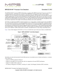
Figure 1-1 shows a block diagram of a 4K core. The MMU can be implemented using either a translation lookaside
buffer (TLB) in the case of the 4Kc core, or a fixed mapping (FM) in the case of the 4Km and 4Kp cores. Refer to Chapter
3, “Memory Management,” on page 31 for more information.
EJTAG
Execution
Core
(RF/ALU/Shift
MMU
System
Coprocessor
TLB or FM
Fixed/Required
Cache
Controller
D-Cache
TAP
BIU
Off-Chip
Debug I/F
On-Chip Bus(es)
I-Cache
Thin I/F
MDU
Power
Mgmt
Optional
Figure 1-1 4K Processor Core Block Diagram
1.3 Required Logic Blocks
The following subsections describe the various required logic blocks of the 4K processor cores.
1.3.1 Execution Unit
The core execution unit implements a load-store architecture with single-cycle Arithmetic Logic Unit (ALU) operations
(logical, shift, add, subtract) and an autonomous multiply-divide unit. The core contains thirty-two 32-bit
general-purpose registers used for scalar integer operations and address calculation. The register file consists of two read
ports and one write port and is fully bypassed to minimize operation latency in the pipeline.
The execution unit includes:
• 32-bit adder used for calculating the data address
• Address unit for calculating the next instruction address
• Logic for branch determination and branch target address calculation
• Load aligner
• Bypass multiplexers used to avoid stalls when executing instruction streams where data-producing instructions are
followed closely by consumers of their results
• Zero/One detect unit for implementing the CLZ and CLO instructions
• ALU for performing bitwise logical operations
4
MIPS32® 4K™ Processor Core Family Software User’s Manual, Revision 01.18
Copyright © 2000-2002 MIPS Technologies Inc. All rights reserved.
1.3 Required Logic Blocks
• Shifter and Store aligner
1.3.2 Multiply/Divide Unit (MDU)
The Multiply/Divide unit performs multiply and divide operations. In the 4Kc and 4Km processors, the MDU consists
of a 32x16 booth-encoded multiplier, result-accumulation registers (HI and LO), a divide state machine, and all
multiplexers and control logic required to perform these functions. This pipelined MDU supports execution of a 16x16
or 32x16 multiply operation every clock cycle; 32x32 multiply operations can be issued every other clock cycle.
Appropriate interlocks are implemented to stall the issue of back-to-back 32x32 multiply operations. Divide operations
are implemented with a simple 1 bit per clock iterative algorithm and require 35 clock cycles in worst case to complete.
Early-in to the algorithm detects sign extension of the dividend, if it is actual size is 24, 16 or 8 bit. the divider will skip
7, 15 or 23 of the 32 iterations. An attempt to issue a subsequent MDU instruction while a divide is still active causes a
pipeline stall until the divide operation is completed.
In the 4Kp processor, the non-pipelined MDU consists of a 32-bit full-adder, result-accumulation registers (HI and LO),
a combined multiply/divide state machine, and all multiplexers and control logic required to perform these functions. It
performs any multiply using 32 cycles in an iterative 1 bit per clock algorithm. Divide operations are also implemented
with a simple 1 bit per clock iterative algorithm (no early-in) and require 35 clock cycles to complete. An attempt to
issue a subsequent MDU instruction while a multiply/divide is still active causes a pipeline stall until the operation is
completed.
An additional multiply instruction, MUL is implemented, which specifies that the lower 32 bits of the multiply result be
placed in the register file instead of the HI/LO register pair. By avoiding the explicit move from LO (MFLO) instruction,
required when using the LO register, and by supporting multiple destination registers, the throughput of
multiply-intensive operations is increased.
Two instructions, multiply-add (MADD/MADDU) and multiply-subtract (MSUB/MSUBU), are used to perform the
multiply-add and multiply-subtract operations. The MADD instruction multiplies two numbers and then adds the
product to the current contents of the HI and LO registers. Similarly, the MSUB instruction multiplies two operands and
then subtracts the product from the HI and LO registers. The MADD/MADDU and MSUB/MSUBU operations are
commonly used in Digital Signal Processor (DSP) algorithms.
1.3.3 System Control Coprocessor (CP0)
In the MIPS architecture, CP0 is responsible for the virtual-to-physical address translation, cache protocols, the
exception control system, the processor’s diagnostics capability, operating mode selection (kernel vs. user mode), and
the enabling/disabling of interrupts. Configuration information such as cache size, set associativity, and EJTAG debug
features are available by accessing the CP0 registers. Refer to Chapter 5, “CP0 Registers,” on page 73 for more
information on the CP0 registers. Refer to Chapter 9, “EJTAG Debug Support,” on page 121 for more information on
EJTAG debug registers.
1.3.4 Memory Management Unit (MMU)
Each The core contains an MMU that interfaces between the execution unit and the cache controller, shown in Figure
1-1. Although the 4Kc core implements a 32-bit architecture, the Memory Management Unit (MMU) is modeled after
the MMU found in the 64-bit R4000 family, as defined by the MIPS32 architecture.
The 4Kc core implements an MMU based on a Translation Lookaside Buffer (TLB). The TLB actually consists of three
translation buffers: a 16 dual-entry fully associative Joint TLB (JTLB), a 3-entry fully associative Instruction TLB
(ITLB) and a 3-entry fully associative data TLB(DTLB). The ITLB and DTLB, also referred to as the micro TLBs, are
managed by the hardware and are not software visible. The micro TLBs contain subsets of the JTLB. When translating
addresses, the corresponding micro TLB (I or D) is accessed first. If there is not a matching entry, the JTLB is used to
MIPS32® 4K™ Processor Core Family Software User’s Manual, Revision 01.18
Copyright © 2000-2002 MIPS Technologies Inc. All rights reserved.
5
Chapter 1 Introduction to the MIPS32 4K™ Processor Core Family
translate the address and refill the micro TLB. If the entry is not found in the JTLB, an exception is taken. To minimize
the micro TLB miss penalty, the JTLB is looked up in parallel with the DTLB for data references. This results in a 1
cycle stall for a DTLB miss and a 2 cycle stall for an ITLB miss.
The 4Km and 4Kp cores implement an FM-based MMU instead of a TLB-based MMU. The FM replaces both the JTLB,
ITLB and DTLB in the 4Kc core. The FM performs a simple translation to get the physical address from the virtual
address. Refer to Chapter 3, “Memory Management,” on page 31 for more information on the FM.
Figure 1-2 shows how the ITLB, DTLB and JTLB are used in the 4Kc core. Figure 1-3 show how the FM is used in the
4Km and 4Kp cores.
Virtual Address
I-Cache
ITLB
Comparator
Instruction
Address
Calculator
IVA
Entry
Instruction
Hit/Miss
Entry
Data
Hit/Miss
JTLB
Data
Address
Calculator
DTLB
Comparator
Virtual Address
D-Cache
Figure 1-2 Address Translation during a Cache Access in the 4Kc Core
6
MIPS32® 4K™ Processor Core Family Software User’s Manual, Revision 01.18
Copyright © 2000-2002 MIPS Technologies Inc. All rights reserved.
1.3 Required Logic Blocks
Virtual Address
Instruction
Address
Calculator
I-Cache
Comparator
Instruction
Hit/Miss
FM
Data
Hit/Miss
Data
Address
Calculator
Comparator
Virtual Address
D-Cache
Figure 1-3 Address Translation during a Cache Access in the 4Km and 4Kp Cores
1.3.5 Cache Controllers
The data and instruction cache controllers support caches of various sizes, organizations, and set associativity. For
example, the data cache can be 2 Kbytes in size and 2-way set associative, while the instruction cache can be 8 Kbytes
in size and 4-way set associative. There are separate cache controllers for the I-Cache and D-Cache.
Each cache controller contains and manages a one-line fill buffer. Besides accumulating data to be written to the cache,
the fill buffer is accessed in parallel with the cache and data can be bypassed back to the core.
Refer to Chapter 7, “Caches,” on page 115 for more information on the instruction and data cache controllers.
1.3.6 Bus Interface Unit (BIU)
The Bus Interface Unit (BIU) controls the external interface signals. Additionally, it contains the implementation of a
32-byte collapsing write-buffer. The purpose of this buffer is to hold and combine write transactions before issuing them
to the external interface. Since the data caches for all cores follow a write-through cache policy, the write-buffer
significantly reduces the number of write transactions on the external interface as well as reducing the amount of stalling
in the core due to issuance of multiple writes in a short period of time.
The write-buffer is organized as two 16-byte buffers. Each buffer contains data from a single 16-byte aligned block of
memory. One buffer contains the data currently being transferred on the external interface, while the other buffer
contains accumulating data from the core.
1.3.7 Power Management
The core offers a number of power management features, including low-power design, active power management, and
power-down modes of operation. The core is a static design that supports a WAIT instruction designed to signal the rest
MIPS32® 4K™ Processor Core Family Software User’s Manual, Revision 01.18
Copyright © 2000-2002 MIPS Technologies Inc. All rights reserved.
7
Chapter 1 Introduction to the MIPS32 4K™ Processor Core Family
of the device that execution and clocking should be halted, hence reducing system power consumption during idle
periods.
The core provides two mechanisms for system-level, low-power support:
• Register-controlled power management
• Instruction-controlled power management
In register controlled power management mode the core provides three bits in the CP0 Status register for software control
of the power management function and allows interrupts to be serviced even when the core is in power-down mode. In
instruction controlled power-down mode execution of the WAIT instruction is used to invoke low-power mode.
Refer to Chapter 8, “Power Management,” on page 119 for more information on power management.
1.4 Optional Logic Blocks
The core consists of the following optional logic blocks as shown in the block diagram in Figure 1-1.
1.4.1 Instruction Cache
The instruction cache is an optional on-chip memory array of up to 16 Kbytes. The cache is virtually indexed and
physically tagged, allowing the virtual-to-physical address translation to occur in parallel with the cache access rather
than having to wait for the physical address translation. The tag holds 22 bits of the physical address, 4 valid bits, a lock
bit, and the LRF (Least Recently Filled) replacement bit.
All cores support instruction cache-locking. Cache locking allows critical code to be locked into the cache on a “per-line”
basis, enabling the system designer to maximize the efficiency of the system cache. Cache locking is always available
on all instruction cache entries. Entries can be marked as locked or unlocked (by setting or clearing the lock-bit) on a
per-entry basis using the CACHE instruction.
1.4.2 Data Cache
The data cache is an optional on-chip memory array of up to 16-Kbytes. The cache is virtually indexed and physically
tagged, allowing the virtual-to-physical address translation to occur in parallel with the cache access. The tag holds 22
bits of the physical address, 4 valid bits, a lock bit, and the LRF replacement bit.
In addition to instruction cache locking, all cores also support a data cache locking mechanism identical to the instruction
cache, with critical data segments to be locked into the cache on a “per-line” basis. The locked contents cannot be
selected for replacement on a cache miss, but can be updated on a store hit.
Cache locking is always available on all data cache entries. Entries can be marked as locked or unlocked on a per-entry
basis using the CACHE instruction.
The physical data cache memory must be byte writable to support non-word store operations.
1.4.3 EJTAG Controller
All cores provide basic EJTAG support with debug mode, run control, single step and software breakpoint instruction
(SDBBP) as part of the core. These features allow for the basic software debug of user and kernel code.
8
MIPS32® 4K™ Processor Core Family Software User’s Manual, Revision 01.18
Copyright © 2000-2002 MIPS Technologies Inc. All rights reserved.
1.4 Optional Logic Blocks
Optional EJTAG features include hardware breakpoints. A 4K core may have four instruction breakpoints and two data
breakpoints, two instruction breakpoints and one data breakpoint, or no breakpoints. The hardware instruction
breakpoints can be configured to generate a debug exception when an instruction is executed anywhere in the virtual
address space. Bit mask and address space identifier (ASID) values may apply in the address compare. These breakpoints
are not limited to code in RAM like the software instruction breakpoint (SDBBP). The data breakpoints can be
configured to generate a debug exception on a data transaction. The data transaction may be qualified with both virtual
address, data value, size and load/store transaction type. Bit mask and ASID values may apply in the address compare,
and byte mask may apply in the value compare.
Refer to Chapter 9, “EJTAG Debug Support,” on page 121 for more information on hardware breakpoints.
An optional Test Access Port (TAP) provides for the communication from an EJTAG probe to the CPU through a
dedicated port, may also be applied to the core. This provides the possibility for debugging without debug code in the
application, and for download of application code to the system.
Refer to Chapter 9, “EJTAG Debug Support,” on page 121 for more information on the EJTAG features.
MIPS32® 4K™ Processor Core Family Software User’s Manual, Revision 01.18
Copyright © 2000-2002 MIPS Technologies Inc. All rights reserved.
9
Chapter 1 Introduction to the MIPS32 4K™ Processor Core Family
10
MIPS32® 4K™ Processor Core Family Software User’s Manual, Revision 01.18
Copyright © 2000-2002 MIPS Technologies Inc. All rights reserved.
Chapter 2
Pipeline
The MIPS32 4K processor cores implements a 5-stage pipeline similar to the original R3000 pipeline. The pipeline
allows the processor to achieve high frequency while minimizing device complexity, reducing both cost and power
consumption. This chapter contains the following sections:
• Section 2.1, "Pipeline Stages"
• Section 2.2, "Instruction Cache Miss"
• Section 2.3, "Data Cache Miss"
• Section 2.4, "Multiply/Divide Operations"
• Section 2.5, "MDU Pipeline (4Kc and 4Km Cores)"
• Section 2.6, "MDU Pipeline (4Kp Core Only)"
• Section 2.7, "Branch Delay"
• Section 2.8, "Data Bypassing"
• Section 2.9, "Interlock Handling"
• Section 2.10, "Slip Conditions"
• Section 2.11, "Instruction Interlocks"
• Section 2.12, "Instruction Hazards"
2.1 Pipeline Stages
The pipeline consists of five stages:
• Instruction (I stage)
• Execution (E stage)
• Memory (M stage)
• Align/Accumulate (A stage)
• Writeback (W stage)
All three cores implement a “Bypass” mechanism that allows the result of an operation to be sent directly to the
instruction that needs it without having to write the result to the register and then read it back.
Figure 2-1 shows the operations performed in each pipeline stage of the 4Kc processor.
MIPS32® 4K™ Processor Core Family Software User’s Manual, Revision 01.18
Copyright © 2000-2002 MIPS Technologies Inc. All rights reserved.
11
Chapter 2 Pipeline
RegW
: I$ Tag and Data read
: I-TLB Look-up
: Instruction Decode
: Register file read
: Instruction Address Calculation stage 1 and 2
: Arithmetic Logic and Shift operations
: Data Address Calculation
: D$ Tag and Data read
: D-TLB Look-up
: Load data aligner
: Register file write or HI/LO write
MUL
: The MUL instruction. Uses MDU-Pipeline write Reg file
I-Cache
I
E
M
A
I-TLB
W
I Dec
A->E Bypass
M->E Bypass
I-AC1
ALU Op
RegRd
I Dec
D-AC
I-AC1
I-AC2
I-AC2
ALU Op
D-Cache
Align
RegW
IU-Pipeline
I-Cache
I-TLB
RegRd
D-TLB
A->E Bypass
MUL
D-AC
D-Cache
D-TLB
Align
Mult, Macc 16x16, 32x16
Mult, Macc
CPA
32x32
CPA
Divide
Sign Adjust
MDU-Pipeline
RegW
RegW
RegW
CPA
Mult, Macc
Divide
Sign Adjust
RegW
: Carry Propagate Adder
: Multiply and Multiply Accumulate instructions
: Divide instructions
: Last stage of Divide is a sign adjustment
: One or more stall cycles.
Figure 2-1 4Kc Core Pipeline Stages
Figure 2-2 shows the operations performed in each pipeline stage of the 4Km processor core.
I
E
M
A
W
D-AC
I-AC1
I-AC2
Align
RegW
A->E Bypass
RegW
Mult, Macc 16x16, 32x16 Carry Prop. Add
RegW
32x32 Carry Prop. Add
Divide
I-AC1
: The MUL instruction. Uses MDU-Pipeline write Reg file
I-AC2
ALU Op
D-AC
D-Cache
Align
MUL
Mult, Macc
IU-Pipeline
D-Cache
I Dec
MUL
RegRd
ALU Op
RegRd
RegW
I Dec
Sign Adjust
RegW
MDU-Pipeline
I-Cache
: I$ Tag and Data read
: Instruction Decode
: Register file read
: Instruction Address Calculation stage 1 and 2
: Arithmetic Logic and Shift operations
: Data Address Calculation
: D$ Tag and Data read
: Load data aligner
: Register file write or HI/LO write
I-Cache
A->E Bypass
M->E Bypass
CPA
Mult, Macc
Divide
Sign Adjust
RegW
: Carry Propagate Adder
: Multiply and Multiply Accumulate instructions
: Divide instructions
: Last stage of Divide is a sign adjustment
: One or more stall cycles.
Figure 2-2 4Km Core Pipeline Stages
Figure 2-3 shows the operations performed in each pipeline stage of the 4Kp processor core.
I
E
M
A
W
I-Cache
A->E Bypass
M->E Bypass
I Dec
RegRd
ALU Op
D-AC
D-Cache
Align
RegW
D-TLB
I-AC1
I-AC2
A->E Bypass
MUL
RegW
Multiply, Divide
RegW
I-AC1
IU-Pipeline
I-TLB
RegRd
MDU-Pipeline
I-Cache
I Dec
I-AC2
ALU Op
D-AC
D-Cache
Align
RegW
MUL
Multiply, Divide
: I$ Tag and Data read
: Instruction Decode
: Register file read
: Instruction Address Calculation stage 1 and 2
: Arithmetic Logic and Shift operations
: Data Address Calculation
: D$ Tag and Data read
: Load data aligner
: Register file write or HI/LO write
: The MUL instruction. Uses MDU-Pipeline, write Reg file
: Multiply, Multiply Accumulate and Divide instructions
: One or more stall cycles.
Figure 2-3 4Kp Core Pipeline Stages
12
MIPS32® 4K™ Processor Core Family Software User’s Manual, Revision 01.18
Copyright © 2000-2002 MIPS Technologies Inc. All rights reserved.
2.1 Pipeline Stages
2.1.1 I Stage: Instruction Fetch
During the Instruction fetch stage:
• An instruction is fetched from the instruction cache.
• The I-TLB performs a virtual-to-physical address translation (4Kc core only).
2.1.2 E Stage: Execution
During the Execution stage:
• Operands are fetched from the register file.
• Operands from M and A stage are bypassed to this stage.
• The Arithmetic Logic Unit (ALU) begins the arithmetic or logical operation for register-to-register instructions.
• The ALU calculates the data virtual address for load and store instructions.
• The ALU determines whether the branch condition is true and calculates the virtual branch target address for branch
instructions.
• Instruction logic selects an instruction address
• All multiply and divide operations begin in this stage.
2.1.3 M Stage: Memory Fetch
During the Memory Fetch stage:
• The arithmetic or logic ALU operation completes.
• The data cache fetch and the data virtual-to-physical address translation are performed for load and store instructions.
• Data TLB (4Kc core only) and data cache lookup are performed and a hit/miss determination is made.
• A 16x16 or 32x16 MUL operation completes in the array and stalls for one clock in the M stage to complete the
carry-propagate-add in the M stage (4Kc and 4Km cores).
• A 32x32 MUL operation stalls for two clocks in the M stage to complete second cycle of the array and the
carry-propagate-add in the M stage (4Kc and 4Km cores).
• A 16x16 or 32x16 MULT/MADD/MSUB operation completes in the array (4Kc and 4Km cores).
• A 32x32 MULT/MADD/MSUB operation stalls for one clock in the MMDU stage of the MDU pipeline to complete
second cycle in the array (4Kc and 4Km cores).
• A divide operation stalls for a maximum of 32 clocks in the MMDU stage of the MDU pipeline (4Kc and 4Km cores).
• A multiply operation stalls for 31 clocks in MMDU stage (4Kp core only).
• A multiply-accumulate operation stalls for 33 clocks in MMDU stage (4Kp core only).
• A divide operation stalls for 32 clocks in the MMDU stage (4Kp core only).
2.1.4 A Stage: Align/Accumulate
During the Align/Accumulate stage:
• A separate aligner aligns loaded data with its word boundary.
MIPS32® 4K™ Processor Core Family Software User’s Manual, Revision 01.18
Copyright © 2000-2002 MIPS Technologies Inc. All rights reserved.
13
Chapter 2 Pipeline
• A MUL operation makes the result available for writeback. The actual register writeback is performed in the W stage
(all 4K cores).
• A MULT/MADD/MSUB operation performs the carry-propagate-add. This includes the accumulate step for the
MADD/MSUB operations. The actual register writeback to HI and LO is performed in the W stage (4Kc and 4Km
cores).
• A divide operation perform the final Sign-Adjust. The actual register writeback to HI and LO is performed in the W
stage (4Kc and 4Km cores).
• A multiply/divide operation writes to HI/LO registers (4Kp core only).
2.1.5 W Stage: Writeback
• For register-to-register or load instructions, the result is written back to the register file during the W stage.
2.2 Instruction Cache Miss
When the instruction cache is indexed, the instruction address is translated to determine if the required instruction resides
in the cache. An instruction cache miss occurs when the requested instruction address does not reside in the instruction
cache. When a cache miss is detected in the I stage, the core transitions to the E stage. The pipeline stalls in the E stage
until the miss is resolved. The bus interface unit must select the address from multiple sources. If the address bus is busy,
the request will remain in this arbitration stage (B-ASel in Figure 2-4 and Figure 2-5) until the bus is available. The core
drives the selected address onto the bus. The number of clocks required to access the bus is determined by the access
time of the array that contains the data. The number of clocks required to return the data once the bus is accessed is also
determined by the access time of the array.
Once the data is returned to the core, the critical word is written to the instruction register for immediate use. The bypass
mechanism allows the core to use the data once it becomes available, as opposed to having the entire cache line written
to the instruction cache, then reading out the required word.
Figure 2-4 shows a timing diagram of an instruction cache miss for the 4Kc core. Figure 2-5 shows a timing diagram of
an instruction cache miss for the 4Km and 4Kp cores.
I
I-Cache
I-TLB
I-TLB
E
B-ASel
E
Bus*
E
IC-Bypass
E
RegRd
I Dec
I-A1
ALU Op
I-A2
* Contains all of the cycles that address and data are utilizing the bus.
Figure 2-4 Instruction Cache Miss Timing (4Kc core)
14
MIPS32® 4K™ Processor Core Family Software User’s Manual, Revision 01.18
Copyright © 2000-2002 MIPS Technologies Inc. All rights reserved.
2.3 Data Cache Miss
E
I
I-Cache
B-ASel
E
Bus*
E
IC-Bypass
E
RegRd
I Dec
I-A1
ALU Op
I-A2
* Contains all of the cycles that address and data are utilizing the bus.
Figure 2-5 Instruction Cache Miss Timing (4Km and 4Kp cores)
2.3 Data Cache Miss
When the data cache is indexed, the data address is translated to determine if the required data resides in the cache. A
data cache miss occurs when the requested data address does not reside in the data cache.
When a data cache miss is detected in the M stage (D-TLB), the core transitions to the A stage. The pipeline stalls in the
A stage until the miss is resolved (requested data is returned). The bus interface unit arbitrates between multiple requests
and selects the correct address to be driven onto the bus (B-ASel in Figure 2-6 and Figure 2-7). The core drives the
selected address onto the bus. The number of clocks required to access the bus is determined by the access time of the
array containing the data. The number of clocks required to return the data once the bus is accessed is also determined
by the access time of the array.
Once the data is returned to the core, the critical word of data passes through the aligner before being forwarded to the
execution unit and register file. The bypass mechanism allows the core to use the data once it becomes available, as
opposed to having the entire cache line written to the data cache, then reading out the required word.
Figure 2-6 shows a timing diagram of a data cache miss for the 4Kc core. Figure 2-7 shows a timing diagram of a data
cache miss for the 4Km and 4Kp cores.
M
E
RegR
ALU1
A
A
A
B-ASel
Bus*
DC Bypass
A
W
D-Cache
D-TLB
Align
RegW
* Contains all of the time that address and data are utilizing the bus.
Figure 2-6 Load/Store Cache Miss Timing (4Kc core)
MIPS32® 4K™ Processor Core Family Software User’s Manual, Revision 01.18
Copyright © 2000-2002 MIPS Technologies Inc. All rights reserved.
15
Chapter 2 Pipeline
M
E
RegR
ALU1
A
A
A
B-ASel
Bus*
DC Bypass
A
W
D-Cache
Align
RegW
* Contains all of the time that address and data are utilizing the bus.
Figure 2-7 Load/Store Cache Miss Timing (4Km and 4Kp cores)
2.4 Multiply/Divide Operations
All three cores implement the standard MIPS II™ multiply and divide instructions. Additionally, several new
instructions were added for enhanced performance.
The targeted multiply instruction, MUL, specifies that multiply results be placed in the general purpose register file
instead of the HI/LO register pair. By avoiding the explicit MFLO instruction, required when using the LO register, and
by supporting multiple destination registers, the throughput of multiply-intensive operations is increased.
Four instructions, multiply-add (MADD), multiply-add-unsigned (MADDU) multiply-subtract (MSUB), and
multiply-subtract-unsigned (MSUBU), are used to perform the multiply-accumulate and multiply-subtract operations.
The MADD/MADDU instruction multiplies two numbers and then adds the product to the current contents of the HI
and LO registers. Similarly, the MSUB/MSUBU instruction multiplies two operands and then subtracts the product from
the HI and LO registers. The MADD/MADDU and MSUB/MSUBU operations are commonly used in DSP algorithms.
All multiply operations (except the MUL instruction) write to the HI/LO register pair. All integer operations write to the
general purpose registers (GPR). Because MDU operations write to different registers than integer operations, following
integer instructions can execute before the MDU operation has completed. The MFLO and MFHI instructions are used
to move data from the HI/LO register pair to the GPR file. If a MFLO or MFHI instruction is issued before the MDU
operation completes, it will stall to wait for the data.
2.5 MDU Pipeline (4Kc and 4Km Cores)
The 4Kc and 4Km processor cores contain an autonomous multiply/divide unit (MDU) with a separate pipeline for
multiply and divide operations. This pipeline operates in parallel with the integer unit (IU) pipeline and does not stall
when the IU pipeline stalls. This allows long-running MDU operations, such as a divide, to be partially masked by
system stalls and/or other integer unit instructions.
The MDU consists of a 32x16 booth encoded multiplier, result/accumulation registers (HI and LO), a divide state
machine, and all necessary multiplexers and control logic. The first number shown (‘32’ of 32x16) represents the rs
operand. The second number (‘16’ of 32x16) represents the rt operand. The core only checks the latter (rt) operand value
to determine how many times the operation must pass through the multiplier. The 16x16 and 32x16 operations pass
through the multiplier once. A 32x32 operation passes through the multiplier twice.
The MDU supports execution of a 16x16 or 32x16 multiply operation every clock cycle; 32x32 multiply operations can
be issued every other clock cycle. Appropriate interlocks are implemented to stall the issue of back-to-back 32x32
multiply operations. Multiply operand size is automatically determined by logic built into the MDU. Divide operations
are implemented with a simple 1 bit per clock iterative algorithm with an early in detection of sign extension on the
16
MIPS32® 4K™ Processor Core Family Software User’s Manual, Revision 01.18
Copyright © 2000-2002 MIPS Technologies Inc. All rights reserved.
2.5 MDU Pipeline (4Kc and 4Km Cores)
dividend (rs). Any attempt to issue a subsequent MDU instruction while a divide is still active causes an IU pipeline stall
until the divide operation is completed.
Table 2-1 lists the latencies (number of cycles until a result is available) for multiply and divide instructions. The
latencies are listed in terms of pipeline clocks. In this table ‘latency’ refers to the number of cycles necessary for the first
instruction to produce the result needed by the second instruction.
Table 2-1 4Kc and 4Km Core Instruction Latencies
Size of operand
1st Instruction[1]
Instruction Sequence
Latency
clocks
1st Instruction
2nd instruction
16 bit
MULT/MULTU,
MADD/MADDU, or
MSUB/MSUBU
MADD/MADDU,
MSUB/MSUBU, or
MFHI/MFLO
1
32 bit
MULT/MULTU,
MADD/MADDU, or
MSUB/MSUBU
MADD/MADDU,
MSUB/MSUBU, or
MFHI/MFLO
2
16 bit
MUL
Integer operation[2]
2[3]
32 bit
MUL
Integer operation[2]
2[3]
8 bit
DIVU
MFHI/MFLO
9
16 bit
DIVU
MFHI/MFLO
17
24 bit
DIVU
MFHI/MFLO
25
32 bit
DIVU
MFHI/MFLO
33
8 bit
DIV
MFHI/MFLO
10[4]
16 bit
DIV
MFHI/MFLO
18[4]
24 bit
DIV
MFHI/MFLO
26[4]
32 bit
DIV
MFHI/MFLO
34[4]
any
MFHI/MFLO
Integer operation[2]
2
any
MTHI/MTLO
MADD/MADDU, or
MSUB/MSUBU
1
Note: [1] For multiply operations this is the rt operand. For divide operations this is the rs operand.
Note: [2] Integer Operation refers to any integer instruction that uses the result of a previous MDU operation.
Note: [3] This does not include the 1 or 2 IU pipeline stalls (16 bit or 32 bit) that MUL operation causes irrespective of
the following instruction.These stalls do not add to the latency of 2.
Note: [4] If both operands are positive the Sign Adjust stage is bypassed. Latency is then the same as for DIVU.
In Table 2-1 a latency of one means that the first and second instruction can be issued back to back in the code without
the MDU causing any stalls in the IU pipeline. A latency of two means that if issued back to back, the IU pipeline will
be stalled for one cycle. MUL operations are special because it needs to stall the IU pipeline in order to maintain its
register file write slot. Consequently the MUL 16x16 or 32x16 operation will always force a one cycle stall of the IU
pipeline, and the MUL 32x32 will force a two cycle stall. If the integer instruction immediately following the MUL
operation uses its result, an additional stall is forced on the IU pipeline.
Table 2-2 lists the repeat rates (peak issue rate of cycles until the operation can be reissued) for multiply
accumulate/subtract instructions. The repeat rates are listed in terms of pipeline clocks. In this table ‘repeat rate’ refers
to the case where the first MDU instruction (in the table below) if back to back with the second instruction.
MIPS32® 4K™ Processor Core Family Software User’s Manual, Revision 01.18
Copyright © 2000-2002 MIPS Technologies Inc. All rights reserved.
17
Chapter 2 Pipeline
Table 2-2 4Kc and 4Km Core Instruction Repeat Rates
Instruction Sequence
Operand Size of
1st Instruction
1st Instruction
2nd instruction
Repeat
Rate
16 bit
MULT/MULTU,
MADD/MADDU,
MSUB/MSUBU
MADD/MADDU,
MSUB/MSUBU
1
32 bit
MULT/MULTU,
MADD/MADDU,
MSUB/MSUBU
MADD/MADDU,
MSUB/MSUBU
2
Figure 2-8 below shows the pipeline flow for the following sequence:
1.
32x16 multiply (Mult1)
2.
Add
3.
32x32 multiply (Mult2)
4.
Sub
The 32x16 multiply operation requires one clock of each pipeline stage to complete. The 32x32 requires two clocks in
the MMDU pipe-stage. The MDU pipeline is shown as the shaded areas of Figure 2-8 and always starts a computation in
the final phase of the E stage. As shown in the figure, the MMDU pipe-stage of the MDU pipeline occurs in parallel with
the M stage of the IU pipeline, the AMDU stage occurs in parallel with the A stage, and the WMDU stage occurs in parallel
with the W stage. However in case the instruction in the MDU pipeline needs multiple passes through the same MDU
stage, this parallel behavior will be skewed by one or more clocks. This is not a problem because results in the MDU
pipeline are written to HI and LO registers, while the integer pipeline results are written to the register file.
Mult1
Add
Mult2
Sub
cycle 1
cycle 2
cycle 3
cycle 4
cycle 5
cycle 6
cycle 7
cycle 8
I
E
MMDU
AMDU
WMDU
I
E
M
A
W
I
E
MMDU
I
E
MMDU
AMDU
WMDU
M
A
W
Figure 2-8 MDU Pipeline Behavior during Multiply Operations (4Kc and 4Km processors)
The following is a cycle-by-cycle analysis of Figure 2-8.
18
1.
The first 32x16 multiply operation (Mult1) enters the I stage and is fetched from the instruction cache.
2.
An Add operation enters the I stage. The Mult1 operation enters the E stage. The integer and MDU pipelines share
the I and E pipeline stages. At the end of the E stage in cycle 2, the multiply operation (Mult1) is passed to the
MDU pipeline.
3.
In cycle 3 a 32x32 multiply operation (Mult2) enters the I stage and is fetched from the instruction cache. Since the
Add operation has not yet reached the M stage by cycle 3, there is no activity in the M stage of the integer pipeline
at this time.
4.
In cycle 4 the Sub instruction enters I stage. The second multiply operation (Mult2) enters the E stage. And the Add
operation enters M stage of the integer pipe. Since the Mult1 multiply is a 32x16 operation, only one clock is
required for the MMDU stage, hence the Mult1 operation passes to the AMDU stage of the MDU pipeline.
MIPS32® 4K™ Processor Core Family Software User’s Manual, Revision 01.18
Copyright © 2000-2002 MIPS Technologies Inc. All rights reserved.
2.5 MDU Pipeline (4Kc and 4Km Cores)
5.
In cycle 5 the Sub instruction enters E stage. The Mult2 multiply enters the MMDU stage. The Add operation enters
the A stage of the integer pipeline. The Mult1 operation completes and is written back in to the HI/LO register pair
in the WMDU stage.
6.
Since a 32x32 multiply requires two passes through the multiplier, with each pass requiring one clock, the 32x32
Mult2 remains in the MMDU stage in cycle 6. The Sub instruction enters M stage in the integer pipeline. The Add
operation completes and is written to the register file in the W stage of the integer pipeline.
7.
The Mult2 multiply operation progresses to the AMDU stage, and the Sub instruction progress to A stage.
8.
The Mult2 operation completes and is written to the HI/LO registers pair the WMDU stage, while the Sub
instruction write to the register file in W stage.
2.5.1 32x16 Multiply (4Kc and 4Km Cores)
The 32x16 multiply operation begins in the last phase of the E stage, which is shared between the integer and MDU
pipelines. In the latter phase of the E stage, the rs and rt operands arrive and the booth recoding function occurs at this
time. The multiply calculation requires one clock and occurs in the MMDU stage. In the AMDU stage, the
carry-propagate-add function occurs and the operation is completed. The result is written back to the HI/LO register pair
in the first half of the WMDU stage.
Figure 2-9 shows a diagram of a 32x16 multiply operation.
Clock
1
2
E
Booth
3
4
MMDU
AMDU
WMDU
Array
CPA
Reg WR
Figure 2-9 MDU Pipeline Flow During a 32x16 Multiply Operation
2.5.2 32x32 Multiply (4Kc and 4Km Cores)
The 32x32 multiply operation begins in the last phase of the E stage, which is shared between the integer and MDU
pipelines. In the latter phase or the E stage, the rs and rt operands arrive and the booth recoding function occurs at this
time. The multiply calculation requires two clocks and occurs in the MMDU stage. In the AMDU stage, the
carry-propagate-add (CPA) function occurs and the operation is completed. The result is written back to the HI/LO
register pair in the first half of the WMDU stage.
Figure 2-10 shows a diagram of a 32x32 multiply operation.
Clock
1
2
E
MMDU
MMDU
AMDU
Array
Array
CPA
Booth
3
4
5
WMDU
Reg WR
Booth
Figure 2-10 MDU Pipeline Flow During a 32x32 Multiply Operation
2.5.3 Divide (4Kc and 4Km Cores)
Divide operations are implemented using a simple non-restoring division algorithm. This algorithm works only for
positive operands, hence the first cycle of the MMDU stage is used to negate the rs operand (RS Adjust) if needed. Note
MIPS32® 4K™ Processor Core Family Software User’s Manual, Revision 01.18
Copyright © 2000-2002 MIPS Technologies Inc. All rights reserved.
19
Chapter 2 Pipeline
that this cycle is executed even if the adjustment is not necessary. At maximum the next 32 clocks (3-34) execute an
iterative add/subtract function. In cycle 3 an early in detection is performed in parallel with the add/subtract. The
adjusted rs operand is detected to be zero extended on the upper most 8, 16 or 24 bits. If this is the case the following 7,
15 or 23 cycles of the add/subtract iterations are skipped.
The remainder adjust (Rem Adjust) cycle is required if the remainder was negative. Note that this cycle is taken even if
the remainder was positive. A sign adjust is performed on the quotient and/or remainder if necessary. Note that the sign
adjust cycle is skipped if both operands are positive. In this case the Rem Adjust is moved to the AMDU stage.
Figure 2-11, Figure 2-12, Figure 2-13 and Figure 2-14 show the latency for 8, 16, 24 and 32-bit divide operations,
respectively. The repeat rate is either 11, 19, 27 or 35 cycles (one less if the sign adjust stage is skipped) as a second
divide can be in the RS Adjust stage when the first divide is in the Reg WR stage.
Clock
1
E Stage
2
3
4-10
11
12
13
WMDU Stage
MMDU Stage
MMDU Stage
MMDU Stage
MMDU Stage
AMDU Stage
RS Adjust
Add/Subtract
Add/Subtract
Rem Adjust
Sign Adjust
Reg WR
Early In
Figure 2-11 MDU Pipeline Flow During an 8-bit Divide (DIV) Operation
Clock
1
E Stage
2
3
4-18
19
20
21
WMDU Stage
MMDU Stage
MMDU Stage
MMDU Stage
MMDU Stage
AMDU Stage
RS Adjust
Add/Subtract
Add/Subtract
Rem Adjust
Sign Adjust
Reg WR
Early In
Figure 2-12 MDU Pipeline Flow During a 16-bit Divide (DIV) Operation
Clock
1
E Stage
2
3
4-26
27
28
29
WMDU Stage
MMDU Stage
MMDU Stage
MMDU Stage
MMDU Stage
AMDU Stage
RS Adjust
Add/Subtract
Add/Subtract
Rem Adjust
Sign Adjust
Reg WR
Early In
Figure 2-13 MDU Pipeline Flow During a 24-bit Divide (DIV) Operation
Clock
1
E Stage
2
3
4-34
35
36
37
MMDU Stage
MMDU Stage
MMDU Stage
MMDU Stage
AMDU Stage
WMDU Stage
RS Adjust
Add/Subtract
Add/Subtract
Rem Adjust
Sign Adjust
Reg WR
Early In
Figure 2-14 MDU Pipeline Flow During a 32-bit Divide (DIV) Operation
20
MIPS32® 4K™ Processor Core Family Software User’s Manual, Revision 01.18
Copyright © 2000-2002 MIPS Technologies Inc. All rights reserved.
2.6 MDU Pipeline (4Kp Core Only)
2.6 MDU Pipeline (4Kp Core Only)
The multiply/divide unit (MDU) is a separate autonomous block for multiply and divide operations. The MDU is not
pipelined, but rather performed the computations iteratively in parallel with the integer unit (IU) pipeline. It does not
stall when the IU pipeline stalls. This allows the long-running MDU operations to be partially masked by system stalls
and/or other integer unit instructions.
The MDU consists of one 32-bit adder result-accumulate registers (HI and LO), a combined multiply/divide state
machine and all multiplexers and control logic. A simple 1-bit per clock recursive algorithm is used for both multiply
and divide operations. Using booth’s algorithm all multiply operations complete in 32 clocks. Two extra clocks are
needed for multiply-accumulate. The non-restoring algorithm used for divide operations will not work with negative
numbers. Adjustment before and after are thus required depending on the sign of the operands. All divide operations
complete in 33 to 35 clocks.
Table 2-3 lists the latencies (number of cycles until a result is available) for multiply and divide instructions. The
latencies are listed in terms of pipeline clocks. In this table ‘latency’ refers to the number of cycles necessary for the
second instruction to use the results of the first.
Table 2-3 4Kp Core Instruction Latencies
Operand Signs of
1st Instruction
(Rs,Rt)
1st Instruction
2nd instruction
any, any
MULT/MULTU
MADD/MADDU,
MSUB/MSUBU, or
MFHI/MFLO
32
any, any
MADD/MADDU,
MSUB/MSUBU
MADD/MADDU,
MSUB/MSUBU, or
MFHI/MFLO
34
any, any
MUL
Integer operation[1]
32
any, any
DIVU
MFHI/MFLO
33
pos, pos
DIV
MFHI/MFLO
33
any, neg
DIV
MFHI/MFLO
34
neg, pos
DIV
MFHI/MFLO
35
any, any
MFHI/MFLO
Integer operation[1]
2
any, any
MTHI/MTLO
MADD/MADDU,
MSUB/MSUBU
1
Instruction Sequence
Latency
clocks
Note: [1] Integer Operation refers to any integer instruction that uses the result of a previous MDU operation.
2.6.1 Multiply (4Kp Core)
Multiply operations implement a simple iterative multiply algorithm. Using Booth’s approach, this algorithm works for
both positive and negative operands. The operation uses 32 cycles in MMDU stage to complete a multiplication. The
register writeback to HI and LO are done in the A stage. For MUL operations, the register file writeback is done in the
WMDU stage.
Figure 2-15 shows the latency for a multiply operation. The repeat rate is 33 cycles as a second multiply can be in the
first MMDU stage when the first multiply is in AMDU stage.
MIPS32® 4K™ Processor Core Family Software User’s Manual, Revision 01.18
Copyright © 2000-2002 MIPS Technologies Inc. All rights reserved.
21
Chapter 2 Pipeline
Clock
1
E-Stage
2-33
MMDU-Stage
Add/sub-shift
34
35
AMDU-Stage
WMDU-Stage
HI/LO Write
Reg WR
Figure 2-15 4Kp MDU Pipeline Flow During a Multiply Operation
2.6.2 Multiply Accumulate (4Kp Core)
Multiply-accumulate operations use the same multiply machine as used for multiply only. Two extra stages are needed
to perform the addition/subtraction. The operations uses 34 cycles in MMDU stage to complete the multiply-accumulate.
The register writeback to HI and LO are done in the A stage.
Figure 2-16 shows the latency for a multiply-accumulate operation. The repeat rate is 35 cycles as a second
multiply-accumulate can be in the E stage when the first multiply is in the last MMDU stage.
Clock
1
2-33
34
E Stage
MMDU Stage
MMDU Stage
Add/Subtract Shift
Accumulate/LO
35
MMDU Stage
Accumulate/HI
36
AMDU Stage
37
WMDU Stage
HI/LO Write
Figure 2-16 4Kp MDU Pipeline Flow During a Multiply Accumulate Operation
2.6.3 Divide (4Kp Core)
Divide operations also implement a simple non-restoring algorithm. This algorithm works only for positive operands,
hence the first cycle of the MMDU stage is used to negate the rs operand (RS Adjust) if needed. Note that this cycle is
executed even if negation is not needed. The next 32 cycle (3-34) executes an interactive add/subtract-shift function.
Two sign adjust (Sign Adjust 1/2) cycles are used to change the sign of one or both the quotient and the remainder. Note
that one or both of these cycles are skipped if they are not needed. The rule is, if both operands were positive or if this
is an unsigned division; both of the sign adjust cycles are skipped. If the rs operand was negative, one of the sign adjust
cycles is skipped. If only the rs operand was negative, none of the sign adjust cycles are skipped. Register writeback to
HI and LO are done in the A stage.
Figure 2-17 shows the latency for a divide operation. The repeat rate is either 34, 35 or 36 cycles (depending on how
many sign adjust cycles are skipped) as a second divide can be in the E stage when the first divide is in the last MMDU
stage.
Clock
1
E Stage
2
3-34
35
36
37
38
MMDU Stage
MMDU Stage
MMDU Stage
MMDU Stage
AMDU Stage
WMDU Stage
RS Adjust
Add/Subtract
Sign Adjust 1
Sign Adjust 2
HI/LO Write
Figure 2-17 4Kp MDU Pipeline Flow During a Divide (DIV) Operation
22
MIPS32® 4K™ Processor Core Family Software User’s Manual, Revision 01.18
Copyright © 2000-2002 MIPS Technologies Inc. All rights reserved.
2.7 Branch Delay
2.7 Branch Delay
The pipeline has a branch delay of one cycle. The one-cycle branch delay is a result of the branch decision logic
operating during the E pipeline stage. This allows the branch target address calculated in the previous stage to be used
for the instruction access in the following E stage. The branch delay slot means that no bubbles are injected into the
pipeline on branch instructions. The address calculation and branch condition check are both performed in the E stage.
The target PC is used for the next instruction in the I stage (2nd instruction after the branch).
The pipeline begins the fetch of either the branch path or the fall-through path in the cycle following the delay slot. After
the branch decision is made, the processor continues with the fetch of either the branch path (for a taken branch) or the
fall-through path (for the non-taken branch).
The branch delay means that the instruction immediately following a branch is always executed, regardless of the branch
direction. If no useful instruction can be placed after the branch, then the compiler or assembler must insert a NOP
instruction in the delay slot.
Figure 2-18 illustrates the branch delay.
One Cycle
One Cycle
One Cycle
One Cycle
One Cycle
I
E
M
A
W
I
E
M
A
W
I
E
M
A
Jump or Branch
Delay Slot Instruction
Jump Target Instruction
One Cycle
One Clock
Branch
Delay
Figure 2-18 IU Pipeline Branch Delay
2.8 Data Bypassing
Most MIPS32 instructions use one or two register values as source operands for the execution. These operands are
fetched from the register file in the first part of E stage. The ALU straddles the E to M boundary, and can present the
result early in M stage. however the result is not written in the register file until W stage. This leaves following
instructions unable to use the result for 3 cycles. To overcome this problem Data bypassing is used.
Between the register file and the ALU a data bypass multiplexer is placed on both operands (see Figure 2-19). This
enables the 4K core to forward data from preceding instructions which have the target register of the first instruction as
one of the source operands. An M to E bypass and an A to E bypass feed the bypass multiplexers. A W to E bypass is
not needed, as the register file is capable of making an internal bypass of Rd write data directly to the Rs and Rt read
ports.
MIPS32® 4K™ Processor Core Family Software User’s Manual, Revision 01.18
Copyright © 2000-2002 MIPS Technologies Inc. All rights reserved.
23
Chapter 2 Pipeline
I stage
E stage
M stage
A stage
W stage
A to E bypass
M to E bypass
Instruction
Rs Addr
Rs Read
Rt Addr
ALU
ALU
Reg File
E stage
M stage
Rd Write
Rt Read
Bypass
multiplexers
Load data, HI/LO Data
or CP0 data
Figure 2-19 IU Pipeline Data Bypass
Figure 2-20 shows the Data bypass for an Add1 instruction followed by a Sub2 and another Add3 instruction. The Sub2
instruction uses the output from the Add1 instruction as one of the operands, and thus the M to E bypass is used. The
following Add3 uses the result from both the first Add1 instruction and the Sub2 instruction. Since the Add1 data is now
in A stage, the A to E bypass is used, and the M to E bypass is used to bypass the Sub2 data to the Add2 instruction.
ADD1
R3=R2+R1
One Cycle
One Cycle
One Cycle
One Cycle
One Cycle
I
E
M
A
W
M to E bypass
I
SUB2
R4=R3-R7
E
One Cycle
A to E bypass
M
A
W
E
M
A
M to E bypass
ADD3
R5=R3+R4
I
Figure 2-20 IU Pipeline M to E bypass
2.8.1 Load Delay
Load delay refers to the fact, that data fetched by a load instruction is not available in the integer pipeline until after the
load aligner in A stage. All instructions need the source operands available in E stage. An instruction immediately
following a load instruction will, if it has the same source register as was the target of the load, cause an instruction
interlock pipeline slip in E stage (see Section 2.11, "Instruction Interlocks" on page 27). If not the first, but the second
instruction after the load, use the data from the load, the A to E bypass (see Figure 2-19) exists to provide for stall free
operation. An instruction flow of this shown in Figure 2-21.
24
MIPS32® 4K™ Processor Core Family Software User’s Manual, Revision 01.18
Copyright © 2000-2002 MIPS Technologies Inc. All rights reserved.
2.9 Interlock Handling
One Cycle
Load Instruction
One Cycle
I
E
One Cycle
One Cycle
One Cycle
A
W
M
One Cycle
Data bypass from A to E
I
E
M
A
W
I
E
M
A
Consumer of Load Data Instruction
One Clock
Load Delay
Figure 2-21 IU Pipeline A to E Data Bypass
2.8.2 Move from HI/LO and CP0 Delay
As indicated in Figure 2-19, not only load data, but also data from a move from the HI or LO register instruction
(MFHI/MFLO) and a move from CP0 (MFC0) enter the IU-Pipeline in A stage. That is, data is not available in the
integer pipeline until early in the A stage. The A to E bypass is available for this data. But as for Loads the instruction
immediately after one of these instructions, can not use this data right away. If it does it will cause an instruction interlock
slip in E stage (see Section 2.11, "Instruction Interlocks" on page 27). An interlock slip after an MFHI is illustrated in
Figure 2-22.
MFHI (to R3)
One Cycle
One Cycle
I
E
One Cycle
M
One Cycle
One Cycle
A
W
One Cycle
One Cycle
Data bypass from A to E
I
ADD (R4=R3+R5)
slip
E
M
A
W
Figure 2-22 IU Pipeline Slip after MFHI
2.9 Interlock Handling
Smooth pipeline flow is interrupted when cache misses occur or when data dependencies are detected. Interruptions
handled using hardware, such as cache misses, are referred to as interlocks. At each cycle, interlock conditions are
checked for all active instructions.
Table 2-4 lists the types of pipeline interlocks for the 4K processor cores.
Table 2-4 Pipeline Interlocks
Interlock Type
Sources
Slip Stage
ITLB Miss (4Kc core)
Instruction TLB
I Stage
ICache Miss
Instruction cache
E Stage
Producer-consumer hazards
E/M Stage
Hardware Dependencies (MDU/TLB)
E Stage
Instruction
MIPS32® 4K™ Processor Core Family Software User’s Manual, Revision 01.18
Copyright © 2000-2002 MIPS Technologies Inc. All rights reserved.
25
Chapter 2 Pipeline
Table 2-4 Pipeline Interlocks (Continued)
Interlock Type
Sources
Slip Stage
DTLB Miss (4Kc core)
Data TLB
M Stage
Load that misses in data cache
Multi-cycle cache Op
Sync
Data Cache Miss
Store when write thru buffer full
W Stage
EJTAG breakpoint on store
VA match needing data value comparison
Store hitting in fill buffer
In general, MIPS processors support two types of hardware interlocks:
• Stalls, which are resolved by halting the pipeline
• Slips, which allow one part of the pipeline to advance while another part of the pipeline is held static
In the 4K processor cores, all interlocks are handled as slips.
2.10 Slip Conditions
On every clock internal logic determines whether each pipe stage is allowed to advance. These slip conditions propagate
backwards down the pipe. For example, if the M stage does not advance, neither will the E or I stages.
Slipped instructions are retried on subsequent cycles until they issue. The back end of the pipeline advances normally
during slips in an attempt to resolve the conflict. NOPS are inserted into the bubble in the pipeline. Figure 2-23 shows
an instruction cache miss.
Clock
1
2
3
1
4
5
2
3
6
Stage
I
I3
I4
I5
I5
I5
I6
E
I2
I3
I4
I4
I4
I5
M
I1
I2
I3
0
0
I4
A
I0
I1
I2
I3
0
0
1 Cache miss detected
2 Critical word received
3 Execute E-stage
Figure 2-23 Instruction Cache Miss Slip
26
MIPS32® 4K™ Processor Core Family Software User’s Manual, Revision 01.18
Copyright © 2000-2002 MIPS Technologies Inc. All rights reserved.
2.11 Instruction Interlocks
Figure 2-23 shows a diagram of a two-cycle slip. In the first clock cycle, the pipeline is full and the cache miss is detected.
Instruction I0 is in the A stage, instruction I1 is in the M stage, instruction I2 is in the E stage, and instruction I3 is in the
I stage. The cache miss occurs in clock 2 when the I4 instruction fetch is attempted. I4 advances to the E-stage and waits
for the instruction to be fetched from main memory. In this example it takes two clocks (3 and 4) to fetch the I4
instruction from memory. Once the cache miss is resolved in clock 4 and the instruction is bypassed to the cache, the
pipeline is restarted, causing the I4 instruction to finally execute it’s E-stage operations.
2.11 Instruction Interlocks
Most instructions can be issued at a rate of one per clock cycle. In some cases, in order to ensure a sequential
programming model, the issue of an instruction is delayed to ensure that the results of a prior instruction will be
available. Table 2-5 details the instruction interactions that delay the issuance of an instruction into the processor
pipeline.
Table 2-5 Instruction Interlocks
Instruction Interlocks
First Instruction
Second Instruction
Issue Delay (in
Clock Cycles)
Slip Stage
LB/LBU/LH/LHU/LL/LW/LWL/LWR
Consumer of load data
1
E stage
MFC0
Consumer of destination
register
1
E stage
0
M stage
1
M stage
2
E stage
3
E stage
1
E stage
2
E stage
1
E stage
0
E stage
1
E stage
MULT/MADD/MSUB
16bx32b
MFLO/MFHI
(4Kc and 4Km cores)
MUL
(4Kc and 4Km cores)
MUL
(4Kc and 4Km cores)
32bx32b
16bx32b
Consumer of target data
32bx32b
16bx32b
Non-Consumer of target data
32bx32b
MFHI/MFLO
Consumer of target data
MULT/MADD/MSUB
(4Kc and 4Km cores)
16bx32b
32bx32b
MULT/MUL/MADD/MSUB
MTHI/MTLO/DIV
DIV
MULT/MUL/MADD/MSUB
/MTHI/MTLO/MFHI/MFL
O/DIV
Until DIV
completes
E stage
MULT/MUL/MADD/MSUB/MTHI/MTLO/
MFHI/MFLO/DIV (4Kp core)
MULT/MUL/MADD/MSUB
/MTHI/MTLO/MFHI/MFL
O/DIV
Until 1st MDU op
completes
E stage
MUL (4Kp core)
Any Instruction
Until MUL
completes
E stage
MFC0
Consumer of target data
1
E stage
2
E stage
1
E stage
TLBWR/TLBWI (4Kc core)
TLBR (4Kc core)
Load/Store/PREF/CACHE/
Cop0 op
MIPS32® 4K™ Processor Core Family Software User’s Manual, Revision 01.18
Copyright © 2000-2002 MIPS Technologies Inc. All rights reserved.
27
Chapter 2 Pipeline
2.12 Instruction Hazards
In general, the core ensures that instructions are executed following a fully sequential program model. Each instruction
in the program sees the results of the previous instruction. There are some exceptions to this model. These exceptions
are referred to as instruction hazards.
The following table shows the instruction hazards that exist in the core. The first and second instruction fields indicate
the combination of instructions that do not ensure a sequential programming model. The Spacing field indicates the
number of unrelated instructions (such as NOPs or SSNOPs) that should be placed between the first and second
instructions of the hazard in order to ensure that the effects of the first instruction are seen by the second instruction.
Entries in the table that are listed as 0 are traditional MIPS hazards which are not hazards on the 4K cores. (MT Compare
to Timer Interrupt cleared is system dependent since Timer Interrupt is an output of the core that can be returned to the
core on one of the SI_Int pins. This number is the minimum time due to going through the core’s I/O registers. Typical
implementations will not add any latency to this).
Table 2-6 Instruction Hazards
Instruction Hazards
Second Instruction
Spacing
(Instructions)
Instruction Fetch Matching Watch Register
2
Load/Store Reference Matching Watch
Register
0
Instruction fetch affected by new page
mapping
3
Load/Store affected by new page mapping
0
TLBP/TLBR
0
TLBR (4Kc core)
Move from Coprocessor Zero Register
0
Move to EntryHi (4Kc core)
TLBWR/TLBWI/TLBP
1
Move to EntryLo0 or EntryLo1 (4Kc core)
TLBWR/TLBWI
0
Move to EntryHi (4Kc core)
Load/Store affected by new ASID
1
Move to EntryHi (4Kc core)
Instruction fetch affected by new ASID
3
TLBP (4Kc core)
Move from Coprocessor Zero Register
0
Move to Index Register
TLBR/TLBWI (4Kc core)
1
Change to CU Bits in Status Register
Coprocessor Instruction
1
Move to EPC, ErrorPC or DEPC
ERET
1
Move to Status Register
ERET
0
Set of IP in Cause Register
Interrupted Instruction
3
Any Other Move to Coprocessor 0 Registers
Instruction Affected by Change
2
CACHE instruction operating on I$
Instruction fetch seeing new cache state
3
LL
Move From LLAddr
1
Move to Compare
Instruction not seeing TimerInterrupt
41
First Instruction
Watch Register Write
TLBWI/TLBWR (4Kc core)
28
MIPS32® 4K™ Processor Core Family Software User’s Manual, Revision 01.18
Copyright © 2000-2002 MIPS Technologies Inc. All rights reserved.
2.12 Instruction Hazards
1. This is the minimum value. Actual value is system-dependent since it is a function of the sequential logic between the SI_TimerInt output
and the external logic which feeds SI_TimerInt back into one of the SI_Int inputs.
MIPS32® 4K™ Processor Core Family Software User’s Manual, Revision 01.18
Copyright © 2000-2002 MIPS Technologies Inc. All rights reserved.
29
Chapter 2 Pipeline
30
MIPS32® 4K™ Processor Core Family Software User’s Manual, Revision 01.18
Copyright © 2000-2002 MIPS Technologies Inc. All rights reserved.
Chapter 3
Memory Management
The MIPS32 4K processor cores contain a Memory Management Unit (MMU) that interfaces between the execution unit
and the cache controller. The MIPS32 4Kc cores contain a Translation Lookaside Buffer (TLB), while the MIPS32 4Km
and MIPS32 4Kp cores implement a simpler Fixed Mapping (FM) style MMU.
This chapter contains the following sections:
• Section 3.1, "Introduction"
• Section 3.2, "Modes of Operation"
• Section 3.3, "Translation Lookaside Buffer (4Kc Core Only)"
• Section 3.4, "Virtual to Physical Address Translation (4Kc Core)"
• Section 3.5, "Fixed Mapping MMU (4Km & 4Kp Cores)"
• Section 3.6, "System Control Coprocessor"
3.1 Introduction
The MMU in a 4K processor core will translate any virtual address to a physical address before a request is sent to the
cache controllers for tag comparison or to the bus interface unit for an external memory reference. This translation is a
very useful feature for operating systems when trying to manage physical memory to accommodate multiple tasks active
in the same memory, possibly on the same virtual address but of course in different locations in physical memory (4Kc
core only). Other features handled by the MMU are protection of memory areas and defining the cache protocol.
In the 4Kc processor core, the MMU is TLB based. The TLB consists of three address translation buffers: a 16 dual-entry
fully associative Joint TLB (JTLB), a 3-entry instruction micro TLB (ITLB), and a 3-entry data micro TLB (DTLB).
When an address is translated, the appropriate micro TLB (ITLB or DTLB) is accessed first. If the translation is not
found in the micro TLB, the JTLB is accessed. If there is a miss in the JTLB, an exception is taken.
In the 4Km and 4Kp processor cores, the MMU is based on a simple algorithm to translate virtual addresses into physical
addresses via a Fixed Mapping (FM) mechanism. These translations are different for various regions of the virtual
address space (useg/kuseg, kseg0, kseg1, kseg2/3).
Figure 3-1 shows how the memory management unit interacts with cache accesses in the 4Kc core, while Figure 3-2
shows how the memory management unit interacts with caches accesses for the 4Km and 4Kp cores. In the 4Km and
4Kp cores, note that the FM MMU replaces the ITLB, DTLB and JTLB found in the 4Kc core.
MIPS32® 4K™ Processor Core Family Software User’s Manual, Revision 01.18
Copyright © 2000-2002 MIPS Technologies Inc. All rights reserved.
31
Chapter 3 Memory Management
Instruction
Cache
RAM
Instruction
Virtual Address
(IVA)
ITLB
IVA
Tag (IPA)
Instruction
Physical
Address
(IPA)
Comparator
Instruction
Hit/Miss
Entry
JTLB
Entry
Data
Virtual Address
(DVA)
DTLB
Data
Cache
RAM
Data
Physical
Address
(DPA)
Data
Hit/Miss
Comparator
Tag (DPA)
Figure 3-1 Address Translation During a Cache Access in the 4Kc Core
Instruction
Cache
RAM
Instruction
Virtual Address
(IVA)
Tag (IPA)
Instruction
Physical
Address
(IPA)
Comparator
Instruction
Hit/Miss
FM MMU
Data
Physical
Address
(DPA)
Data
Virtual Address
(DVA)
Data
Hit/Miss
Comparator
Data
Cache
RAM
Tag (DPA)
Figure 3-2 Address Translation During a Cache Access in the 4Km and 4Kp cores
3.2 Modes of Operation
All The 4K processor cores supports three modes of operation:
32
MIPS32® 4K™ Processor Core Family Software User’s Manual, Revision 01.18
Copyright © 2000-2002 MIPS Technologies Inc. All rights reserved.
3.2 Modes of Operation
• User mode
• Kernel mode
• Debug mode
User mode is most often used for application programs. Kernel mode is typically used for handling exceptions and
privileged operating system functions, including CP0 management and I/O device accesses. Debug mode is used for
software debugging and most likely occurs within a software development tool.
The address translation performed by the MMU depends on the mode in which the processor is operating.
3.2.1 Virtual Memory Segments
The Virtual memory segments are different depending on the mode of operation. Figure 3-3 shows the segmentation for
the 4 GByte (232 bytes) virtual memory space addressed by a 32-bit virtual address, for the three modes of operation.
The core enters Kernel mode both at reset and when an exception is recognized. While in Kernel mode, software has
access to the entire address space, as well as all CP0 registers. User mode accesses are limited to a subset of the virtual
address space (0x0000_0000 to 0x7FFF_FFFF) and can be inhibited from accessing CP0 functions. In User mode,
virtual addresses 0x8000_0000 to 0xFFFF_FFFF are invalid and cause an exception if accessed.
Debug mode is entered on a debug exception. While in Debug mode, the debug software has access to the same address
space and CP0 registers as for Kernel mode. In addition, while in Debug mode the core has access to the debug segment
dseg. This area overlays part of the kernel segment kseg3. dseg access in Debug mode can be turned on or off, allowing
full access to the entire kseg3 in Debug mode, if so desired.
MIPS32® 4K™ Processor Core Family Software User’s Manual, Revision 01.18
Copyright © 2000-2002 MIPS Technologies Inc. All rights reserved.
33
Chapter 3 Memory Management
User Mode
Virtual Address
Kernel Mode
0xFFFF_FFFF
Debug Mode
kseg3
0xF400_0000
0xF3FF_FFFF
kseg3
dseg
kseg3
0xF200_0000
0xF1FF_FFFF
0xE000_0000
0xDFFF_FFFF
kseg2
kseg2
0xC000_0000
0xBFFF_FFFF
kseg1
kseg1
kseg0
kseg0
kuseg
kuseg
0xA000_0000
0x9FFF_FFFF
0x8000_0000
0x7FFF_FFFF
useg
0x0000_0000
Figure 3-3 4K Processor Core Virtual Memory Map
Each of the segments shown in Figure 3-3 is either mapped or unmapped. The following two subsections explain the
distinction. Then Section 3.2.2, "User Mode", Section 3.2.3, "Kernel Mode" and Section 3.2.4, "Debug Mode" specify
which segments are actually mapped and unmapped.
3.2.1.1 Unmapped Segments
An unmapped segment does not use the TLB (4Kc core) or the FM (4Km and 4Kp cores) to translate from virtual to
physical address. Especially after reset it is important to have unmapped memory segments, because the TLB is not yet
programmed to perform the translation.
Unmapped segments have a fixed simple translation from virtual to physical address. This is much like the translations
the FM provides for the 4Km and 4Kp cores, but we will still make the distinction.
Except for kseg0, unmapped segments are always uncached. The cacheability of kseg0 is set in the K0 field of the CP0
register Config (see Section 5.2.15, "Config Register (CP0 Register 16, Select 0)").
34
MIPS32® 4K™ Processor Core Family Software User’s Manual, Revision 01.18
Copyright © 2000-2002 MIPS Technologies Inc. All rights reserved.
3.2 Modes of Operation
3.2.1.2 Mapped Segments
A mapped segment does use the TLB (4Kc core) or the FM (4Km and 4Kp cores) to translate from virtual to physical
address.
For the 4Kc core, the translation of mapped segments is handled on a per-page basis. Included in this translation is
information defining whether the page is cacheable or not, and the protection attributes that apply to the page.
For the 4Km and 4Kp cores, the mapped segments have a fixed translation from virtual to physical address. The
cacheability of the segment is defined in the CP0 register Config, fields K23 and KU (see Section 5.2.15, "Config
Register (CP0 Register 16, Select 0)"). Write protection of segments is not possible during FM translation.
3.2.2 User Mode
In user mode, a single 2 GByte (231 bytes) uniform virtual address space called the user segment (useg) is available.
Figure 3-4 shows the location of user mode virtual address space.
32 bit
0xFFFF_FFFF
Address
Error
0x8000_0000
0x7FFF_FFFF
2GB
Mapped
useg
0x0000_0000
Figure 3-4 User Mode Virtual Address Space
The user segment starts at address 0x0000_0000 and ends at address 0x7FFF_FFFF. Accesses to all other addresses
cause an address error exception.
The processor operates in User mode when the Status register contains the following bit values:
• UM = 1
• EXL = 0
• ERL = 0
In addition to the above values, the DM bit in the Debug register must be 0.
Table 3-1 lists the characteristics of the useg User mode segments.
MIPS32® 4K™ Processor Core Family Software User’s Manual, Revision 01.18
Copyright © 2000-2002 MIPS Technologies Inc. All rights reserved.
35
Chapter 3 Memory Management
Table 3-1 User Mode Segments
Status Register
Address
Bit Value
Bit Value
Segment
EXL
ERL
UM
Name
0
0
1
useg
32-bit
A(31) = 0
Address Range
Segment Size
0x0000_0000 -->
2 GByte
(231 bytes)
0x7FFF_FFFF
All valid user mode virtual addresses have their most-significant bit cleared to 0, indicating that user mode can only
access the lower half of the virtual memory map. Any attempt to reference an address with the most-significant bit set
while in user mode causes an address error exception.
The system maps all references to useg through the TLB (4Kc core) or FM (4Km and 4Kp cores). For the 4Kc core, the
The virtual address is extended with the contents of the 8-bit ASID field to form a unique virtual address before
translation. Bit settings within the TLB entry for the page determine the cacheability of a reference. For the 4Km and
4Kp cores, the cacheability is set via the KU field of the CP0 Config register.
3.2.3 Kernel Mode
The processor operates in Kernel mode when the DM bit in the Debug register is 0 and the Status register contains one
or more of the following values:
• UM = 0
• ERL = 1
• EXL = 1
When a non-debug exception is detected, EXL or ERL will be set and the processor will enter Kernel mode. At the end
of the exception handler routine, an Exception Return (ERET) instruction is generally executed. The ERET instruction
jumps to the Exception PC, clears ERL, and clears EXL if ERL=0. This may return the processor to User mode.
Kernel mode virtual address space is divided into regions differentiated by the high-order bits of the virtual address, as
shown in Figure 3-5. Also, Table 3-2 lists the characteristics of the Kernel mode segments.
36
MIPS32® 4K™ Processor Core Family Software User’s Manual, Revision 01.18
Copyright © 2000-2002 MIPS Technologies Inc. All rights reserved.
3.2 Modes of Operation
0xFFFF_FFFF
0xE000_0000
0xDFFF_FFFF
0xC000_0000
0xBFFF_FFFF
Kernel virtual address space
Mapped, 512MB
kseg3
Kernel virtual address space
Mapped, 512MB
kseg2
Kernel virtual address space
Unmapped,
Uncached, 512MB
0xA000_0000
0x9FFF_FFFF
Kernel virtual address space
Unmapped, 512MB
0x8000_0000
0x7FFF_FFFF
Mapped, 2048MB
kseg1
kseg0
kuseg
0x0000_0000
Figure 3-5 Kernel Mode Virtual Address Space
Table 3-2 Kernel Mode Segments
Address Bit
Values
Status Register Is
One of These Values
UM
EXL
A(31) = 0
ERL
Segment
Name
Address Range
Segment
Size
kuseg
0x0000_0000
through
0x7FFF_FFFF
2 GBytes
(231 bytes)
kseg0
0x8000_0000
through
0x9FFF_FFFF
512 MBytes
(229 bytes)
kseg1
0xA000_0000
through
0xBFFF_FFFF
512 MBytes
(229 bytes)
kseg2
0xC000_0000
through
0xDFFF_FFFF
512 MBytes
(229 bytes)
kseg3
0xE000_0000
through
0xFFFF_FFFF
512 MBytes
(229 bytes)
(UM = 0
A(31:29) = 1002
or
EXL = 1
A(31:29) = 1012
or
ERL = 1)
A(31:29) = 1102
and
DM = 0
A(31:29) = 1112
MIPS32® 4K™ Processor Core Family Software User’s Manual, Revision 01.18
Copyright © 2000-2002 MIPS Technologies Inc. All rights reserved.
37
Chapter 3 Memory Management
3.2.3.1 Kernel Mode, User Space (kuseg)
In Kernel mode, when the most-significant bit of the virtual address (A31) is cleared, the 32-bit kuseg virtual address
space is selected and covers the full 231 bytes (2 GByte) of the current user address space mapped to addresses
0x0000_0000 - 0x7FFF_FFFF. For the 4Kc core, the virtual address is extended with the contents of the 8-bit ASID field
to form a unique virtual address.
When ERL = 1 in the Status register, the user address region becomes a 231-byte unmapped and uncached address space.
While in this setting, the kuseg virtual address maps directly to the same physical address, and does not include the ASID
field.
3.2.3.2 Kernel Mode, Kernel Space 0 (kseg0)
In Kernel mode, when the most-significant three bits of the virtual address are 1002, 32-bit kseg0 virtual address space
is selected; it is the 229-byte (512-MByte) kernel virtual space located at addresses 0x8000_0000 - 0x9FFF_FFFF.
References to kseg0 are unmapped; the physical address selected is defined by subtracting 0x8000_0000 from the virtual
address. The K0 field of the Config register controls cacheability.
3.2.3.3 Kernel Mode, Kernel Space 1 (kseg1)
In Kernel mode, when the most-significant three bits of the 32-bit virtual address are 1012, 32-bit kseg1 virtual address
space is selected. kseg1 is the 229-byte (512-MByte) kernel virtual space located at addresses 0xA000_0000 0xBFFF_FFFF. References to kseg1 are unmapped; the physical address selected is defined by subtracting
0xA000_0000 from the virtual address. Caches are disabled for accesses to these addresses, and physical memory (or
memory-mapped I/O device registers) are accessed directly.
3.2.3.4 Kernel Mode, Kernel Space 2 (kseg2)
In Kernel mode, when UM = 0, ERL = 1, or EXL = 1 in the Status register, and DM = 0 in the Debug register, and the
most-significant three bits of the 32-bit virtual address are 1102, 32-bit kseg2 virtual address space is selected. This
229-byte (512-MByte) kernel virtual space is located at physical addresses 0xC000_0000 - 0xDFFF_FFFF in the 4Km
and 4Kp processor cores. This space is mapped through the TLB in the 4Kc processor core.
3.2.3.5 Kernel Mode, Kernel Space 3 (kseg3)
In Kernel mode, when the most-significant three bits of the 32-bit virtual address are 1112, the kseg3 virtual address
space is selected. This 229-byte (512-MByte) kernel virtual space is located at physical addresses 0xE000_0000 0xFFFF_FFFF in the 4Km and 4Kp processor cores. This space is mapped through the TLB in the 4Kc processor core.
3.2.4 Debug Mode
Debug mode address space is identical to Kernel mode address space with respect to mapped and unmapped areas,
except for kseg3. In kseg3, a debug segment dseg co-exists in the virtual address range 0xFF20_0000 to 0xFF3F_FFFF.
The layout is shown in Figure 3-6.
38
MIPS32® 4K™ Processor Core Family Software User’s Manual, Revision 01.18
Copyright © 2000-2002 MIPS Technologies Inc. All rights reserved.
3.2 Modes of Operation
0xFFFF_FFFF
0xFF40_0000
dseg
0xFF20_0000
kseg1
kseg0
Unmapped
Mapped if mapped in Kernel Mode
0x0000_0000
Figure 3-6 Debug Mode Virtual Address Space
The dseg is sub-divided into the dmseg segment at 0xFF20_0000 to 0xFF2F_FFFF which is used when the probe
services the memory segment, and the drseg segment at 0xFF30_0000 to 0xFF3F_FFFF which is used when memory
mapped debug registers are accessed. The subdivision and attributes for the segments are shown in Table 3-3.
Accesses to memory that would normally cause an exception if tried from kernel mode cause the core to re-enter debug
mode via a debug mode exception. This includes accesses usually causing a TLB exception (4Kc core only), with the
result that such accesses are not handled by the usual memory management routines.
The unmapped kseg0 and kseg1 segments from kernel mode address space are available from debug mode, which allows
the debug handler to be executed from uncached and unmapped memory.
Table 3-3 Physical Address and Cache Attributes for dseg, dmseg, and drseg Address Spaces
Segment
Name
Sub-Segment
Name
Virtual Address
Generates Physical Address
Cache
Attribute
0xFF20_0000
dmseg
through
0xFF2F_FFFF
dmseg maps to addresses
0x0_0000 - 0xF_FFFF in EJTAG
probe memory space.
dseg
Uncached
0xFF30_0000
drseg
drseg maps to the breakpoint
registers 0x0_0000 - 0xF_FFFF
through
0xFF3F_FFFF
3.2.4.1 Conditions and Behavior for Access to drseg, EJTAG Registers
The behavior of CPU access to the drseg address range at 0xFF30_0000 to 0xFF3F_FFFF is determined as shown in
Table 3-4.
Table 3-4 CPU Access to drseg Address Range
Transaction
LSNM bit in Debug
register
Load / Store
1
Fetch
Don’t care
Load / Store
0
Access
Kernel mode address space (kseg3)
drseg, see comments below
MIPS32® 4K™ Processor Core Family Software User’s Manual, Revision 01.18
Copyright © 2000-2002 MIPS Technologies Inc. All rights reserved.
39
Chapter 3 Memory Management
Debug software is expected to read the debug control register (DCR) to determine which other memory mapped registers
exist in drseg. The value returned in response to a read of any unimplemented memory mapped register is unpredictable,
and writes are ignored to any unimplemented register in the drseg. Refer to Chapter 9, “EJTAG Debug Support,” on page
121 for more information on the DCR.
The allowed access size is limited for the drseg. Only word size transactions are allowed. Operation of the processor is
undefined for other transaction sizes.
3.2.4.2 Conditions and Behavior for Access to dmseg, EJTAG Memory
The behavior of CPU access to the dmseg address range at 0xFF20_0000 to 0xFF2F_FFFF is determined by Table 3-5.
.
Table 3-5 CPU Access to dmseg Address Range
Transaction
ProbEn bit in
DCR register
LSNM bit in
Debug register
Load / Store
Don’t care
1
Fetch
1
Don’t care
Load / Store
1
0
Fetch
0
Don’t care
Load / Store
0
0
Access
Kernel mode address space (kseg3)
dmseg
See comments below
The case with access to the dmseg when the ProbEn bit in the DCR register is 0 is not expected to happen. Debug
software is expected to check the state of the ProbEn bit in DCR register before attempting to reference dmseg. If such
a reference does happen, the reference hangs until it is satisfied by the probe. The probe can not assume that there will
never be a reference to dmseg if the ProbEn bit in the DCR register is 0 because there is an inherent race between the
debug software sampling the ProbEn bit as 1 and the probe clearing it to 0.
3.3 Translation Lookaside Buffer (4Kc Core Only)
The following subsections discuss the TLB memory management scheme used in the 4Kc processor core. The TLB
consists of one joint and two micro address translation buffers:
• 16 dual-entry fully associative Joint TLB (JTLB)
• 3-entry fully associative Instruction micro TLB (ITLB)
• 3-entry fully associative Data micro TLB (DTLB)
3.3.1 Joint TLB
The 4Kc core implements a 16 dual-entry, fully associative Joint TLB that maps 32 virtual pages to their corresponding
physical addresses. The JTLB is organized as 16 pairs of even and odd entries containing pages that range in size from
4-KBytes to 16-MBytes into the 4-GByte physical address space. The purpose of the TLB is to translate virtual addresses
and their corresponding Address Space Identifier (ASID) into a physical memory address. The translation is performed
by comparing the upper bits of the virtual address (along with the ASID bits) against each of the entries in the tag portion
of the JTLB structure. Because this structure is used to translate both instruction and data virtual addresses, it is referred
to as a “joint” TLB.
The JTLB is organized in page pairs to minimize its overall size. Each virtual tag entry corresponds to two physical data
entries, an even page entry and an odd page entry. The highest order virtual address bit not participating in the tag
40
MIPS32® 4K™ Processor Core Family Software User’s Manual, Revision 01.18
Copyright © 2000-2002 MIPS Technologies Inc. All rights reserved.
3.3 Translation Lookaside Buffer (4Kc Core Only)
comparison is used to determine which of the two data entries is used. Since page size can vary on a page-pair basis, the
determination of which address bits participate in the comparison and which bit is used to make the even-odd
determination must be determined dynamically during the TLB lookup.
Figure 3-7 show the contents of one of the 16 dual-entries in the JTLB.
PageMask[24:13]
Tag Entry
VPN2[31:13]
GG
ASID[7:0]
19
1
8
PFN0[31:12]
C0[2:0]
D0
V0
PFN1[31:12]
C1[2:0]
D1
V1
20
3
1
1
Data Entries
Figure 3-7 JTLB Entry (Tag and Data)
Table 3-6 and Table 3-7 explain each of the fields in a JTLB entry.
Table 3-6 TLB Tag Entry Fields
Field Name
Description
Page Mask Value. The Page Mask defines the page size by masking the
appropriate VPN2 bits from being involved in a comparison. It is also used to
determine which address bit is used to make the even-odd page (PFN0-PFN1)
determination. See the table below.
PageMask[11:0]
PageMask[24:13]
Page Size
Even/Odd Bank
Select Bit
0000_0000_0000
4KB
VAddr[12]
0000_0000_0011
16KB
VAddr[14]
0000_0000_1111
64KB
VAddr[16]
0000_0011_1111
256KB
VAddr[18]
0000_1111_1111
1MB
VAddr[20]
0011_1111_1111
4MB
VAddr[22]
1111_1111_1111
16MB
VAddr[24]
The PageMask column above show all the legal values for PageMask. Because
each pair of bits can only have the same value, the physical entry in the JTLB
will only save a compressed version of the PageMask using only 6 bits. This is
however transparent to software, which will always work with a 12 bit field.
VPN2[31:13]
Virtual Page Number divided by 2. This field contains the upper bits of the
virtual page number. Because it represents a pair of TLB pages, it is divided by
2. Bits 31:25 are always included in the TLB lookup comparison. Bits 24:13
are included depending on the page size, defined by PageMask.
G
Global Bit. When set, indicates that this entry is global to all processes and/or
threads and thus disables inclusion of the ASID in the comparison.
ASID[7:0]
Address Space Identifier. Identifies which process or thread this TLB entry is
associated with.
MIPS32® 4K™ Processor Core Family Software User’s Manual, Revision 01.18
Copyright © 2000-2002 MIPS Technologies Inc. All rights reserved.
41
Chapter 3 Memory Management
Table 3-7 TLB Data Entry Fields
Field Name
Description
PFN0[31:12],
PFN1[31:12]
Physical Frame Number. Defines the upper bits of the physical address.
For page sizes larger than 4 KBytes, only a subset of these bits is actually
used.
Cacheability. Contains an encoded value of the cacheability attributes and
determines whether the page should be placed in the cache or not. The field
is encoded as follows:
C[2:0]
C0[2:0],
C1[2:0]
Coherency Attribute
000
Maps to entry 011b*
001
Maps to entry 011b*
010
Uncached
011
Cacheable, noncoherent, write-through,
no write allocated
100
Maps to entry 011b*
101
Maps to entry 011b*
110
Maps to entry 011b*
111
Maps to entry 010b*
Note: * These mappings are not used on the 4K processor cores but do have meaning in other MIPS
D0,
D1
“Dirty” or Write-enable Bit. Indicates that the page has been written,
and/or is writable. If this bit is set, stores to the page are permitted. If the
bit is cleared, stores to the page cause a TLB Modified exception.
V0,
V1
Valid Bit. Indicates that the TLB entry and, thus, the virtual page mapping
are valid. If this bit is set, accesses to the page are permitted. If the bit is
cleared, accesses to the page cause a TLB Invalid exception.
In order to fill an entry in the JTLB, software executes a TLBWI or TLBWR instruction (See Section 3.4.3, "TLB
Instructions" on page 47). Prior to invoking one of these instructions, several CP0 registers must be updated with the
information to be written to a TLB entry.
• PageMask is set in the CP0 PageMask register.
• VPN2 and ASID are set in the CP0 EntryHi register.
• PFN0, C0, D0, V0 and G bit are set in the CP0 EntryLo0 register.
• PFN1, C1, D1, V1 and G bit are set in the CP0 EntryLo1 register.
Note that the global bit “G” is part of both EntryLo0 and EntryLo1. The resulting “G” bit in the JTLB entry is the logical
AND between the two fields in EntryLo0 and EntryLo1. Please refer to Chapter 5, “CP0 Registers,” on page 73 for
further details.
The address space identifier (ASID) helps to reduce the frequency of TLB flushing on a context switch. The existence
of the ASID allows multiple processes to exist in both the TLB and instruction caches. The ASID value is stored in the
EntryHi register and is compared to the ASID value of each entry.
3.3.2 Instruction TLB
The ITLB is a small 3-entry, fully associative TLB dedicated to performing translations for the instruction stream. The
ITLB only maps 4-Kbyte pages/sub-pages.
42
MIPS32® 4K™ Processor Core Family Software User’s Manual, Revision 01.18
Copyright © 2000-2002 MIPS Technologies Inc. All rights reserved.
3.4 Virtual to Physical Address Translation (4Kc Core)
The ITLB is managed by hardware and is transparent to software. If a fetch address cannot be translated by the ITLB,
the JTLB is accessed to attempt to translate it in the following clock cycle. If successful, the translation information is
copied into the ITLB. The ITLB is then re-accessed and the address will be successfully translated. This results in an
ITLB miss penalty of at least 2 cycles (if the JTLB is busy with other operations, it may take additional cycles).
3.3.3 Data TLB
The DTLB is a small 3-entry, fully associative TLB which provides a faster translation for Load/Store addresses than is
possible with the JTLB. The DTLB only maps 4-Kbyte pages/sub-pages.
Like the ITLB, the DTLB is managed by hardware and is transparent to software. Unlike the ITLB, when translating
Load/Store addresses, the JTLB is accessed in parallel with the DTLB. If there is a DTLB miss and a JTLB hit, the DTLB
can be reloaded that cycle. The DTLB is then re-accessed and the translation will be successful. This parallel access
reduces the DTLB miss penalty to 1 cycle.
3.4 Virtual to Physical Address Translation (4Kc Core)
Converting a virtual address to a physical address begins by comparing the virtual address from the processor with the
virtual addresses in the TLB. There is a match when the virtual page number (VPN) of the address is the same as the
VPN field of the entry, and either:
• The Global (G) bit of both the even and odd pages of the TLB entry are set, or
• The ASID field of the virtual address is the same as the ASID field of the TLB entry
This match is referred to as a TLB hit. If there is no match, a TLB miss exception is taken by the processor and software
is allowed to refill the TLB from a page table of virtual/physical addresses in memory.
Figure 3-8 shows the logical translation of a virtual address into a physical address.
In this figure the virtual address is extended with an 8-bit address-space identifier (ASID), which reduces the frequency
of TLB flushing during a context switch. This 8-bit ASID contains the number assigned to that process and is stored in
the CP0 EntryHi register.
MIPS32® 4K™ Processor Core Family Software User’s Manual, Revision 01.18
Copyright © 2000-2002 MIPS Technologies Inc. All rights reserved.
43
Chapter 3 Memory Management
Virtual Address
1.Virtual address (VA) represented by
the virtual page number (VPN) is
compared with tag in TLB.
2. If there is a match, the page frame
number (PFN0 or PFN1)
representing the upper bits of the
physical address (PA) is output from
the TLB.
G
ASID
VPN
G
ASID
VPN2
C0 D0 V0
PFN0
C1 D1 V1
PFN1
Offset
TLB
Entry
TLB
3. The Offset, which does not pass
through the TLB, is then concatenated
with the PFN.
PFN
Offset
Physical Address
Figure 3-8 Overview of a Virtual-to-Physical Address Translation in the 4Kc Core
If there is a virtual address match in the TLB, the physical frame number (PFN) is output from the TLB and concatenated
with the Offset, to form the physical address. The Offset represents an address within the page frame space. As shown in
Figure 3-8, the Offset does not pass through the TLB.
Figure 3-9 shows a flow diagram of the 4Kc core address translation process. The top portion of the figure shows a virtual
address for a 4-KByte page size. The width of the Offset is defined by the page size. The remaining 20 bits of the address
represent the virtual page number (VPN), that index the 1M-entry page table.
The bottom portion of Figure 3-9 shows the virtual address for a 16-MByte page size. The remaining 8 bits of the address
represent the VPN, that index the 256-entry page table.
44
MIPS32® 4K™ Processor Core Family Software User’s Manual, Revision 01.18
Copyright © 2000-2002 MIPS Technologies Inc. All rights reserved.
3.4 Virtual to Physical Address Translation (4Kc Core)
39
Virtual address with 1M (220) 4-KByte pages
20 bits = 1M pages
32 31
12 11
ASID
VPN
Offset
8
20
12
Offset passed unchanged
to physical memory.
Virtual-to-physical
translation in TLB
Bit 31 of the virtual address
selects user and kernel
address spaces.
TLB
32-bit Physical Address
31
0
PFN0/1
Offset
Virtual-to-physical
translation in TLB
Offset passed unchanged
to physical memory.
TLB
39
32 31
ASID
8
0
24 23
0
VPN
Offset
8
24
8 bits = 256 pages
Virtual Address with 256 (28)16-MByte pages
Figure 3-9 32-bit Virtual Address Translation
3.4.1 Hits, Misses, and Multiple Matches
Each JTLB entry contains a tag and two data fields. If a match is found, the upper bits of the virtual address are replaced
with the page frame number (PFN) stored in the corresponding entry in the data array of the JTLB. The granularity of
JTLB mappings is defined in terms of TLB pages. The 4Kc core JTLB supports pages of different sizes ranging from
4-KB to 16-MB in powers of 4. If a match is found, but the entry is invalid (i.e., the V bit in the data field is 0), a TLB
Invalid exception is taken.
If no match occurs (TLB miss), an exception is taken and software refills the TLB from the page table resident in
memory. Figure 3-10 show the translation and exception flow of the TLB.
Software can write over a selected TLB entry or use a hardware mechanism to write into a random entry. The Random
register selects which TLB entry to use on a TLBWR. This register decrements almost every cycle, wrapping to the
maximum once it’s value is equal to the Wired register. Thus, TLB entries below the Wired value cannot be replaced by
a TLBWR allowing important mappings to be preserved. In order to reduce the possibility for a livelock situation, the
Random register includes a 10b LFSR that introduces a pseudo-random perturbation into the decrementing.
The 4Kc core implements a TLB write-compare mechanism to ensure that multiple TLB matches do not occur. On the
TLB write operation, the VPN2 field to be written is compared with all other entries in the TLB. If a match occurs, the
4Kc core takes a machine-check exception, sets the TS bit in the CP0 Status register, and aborts the write operation. For
further details on exceptions, please refer to Chapter 4, “Exceptions,” on page 51. There is a hidden bit in each TLB entry
that is cleared on a ColdReset. This bit is set once the TLB entry is written and is included in the match detection.
Therefore, uninitialized TLB entries will not cause a TLB shutdown.
Note: This hidden initialization bit leaves the entire JTLB invalid after a ColdReset, eliminating the need to flush the
TLB. But, to be compatible with other MIPS processors, it is recommended that software initialize all TLB entries with
unique tag values and V bits cleared before the first access to a mapped location.
MIPS32® 4K™ Processor Core Family Software User’s Manual, Revision 01.18
Copyright © 2000-2002 MIPS Technologies Inc. All rights reserved.
45
Chapter 3 Memory Management
3.4.2 Page Sizes and Replacement Algorithm
To assist in controlling both the amount of mapped space and the replacement characteristics of various memory regions,
the 4Kc core provides two mechanisms. First, the page size can be configured, on a per entry basis, to map page sizes
ranging from 4 KByte to 16 MByte (in multiples of 4). The CP0 PageMask register is loaded with the desired page size,
which is then entered into the TLB when a new entry is written. Thus, operating systems can provide special-purpose
maps. For example, a typical frame buffer can be memory mapped with only one TLB entry.
The second mechanism controls the replacement algorithm when a TLB miss occurs. To select a TLB entry to be written
with a new mapping, the 4Kc core provides a random replacement algorithm. However, the processor also provides a
mechanism whereby a programmable number of mappings can be locked into the TLB via the CP0 Wired register, thus
avoiding random replacement. Please refer to Section 5.2.6, "Wired Register (CP0 Register 6, Select 0)" on page 82 for
further details.
Virtual Address (Input)
For valid address
space, see the section
describing Modes of
operation in this
chapter.
Address
Error
VPN
and
ASID
User
Address?
No
Exception
Yes
User
Mode?
No
Yes
Unmapped
Address
kseg0/kseg1
Address
Yes
No
No
VPN
Match?
Yes
Global
No
G = 1?
Yes
ASID
Match?
No
Yes
Valid
No
V = 1?
Yes
Dirty
Yes
No
Write?
D = 1?
No
TLB
Modified
Yes
Noncacheable
Yes
C=010
or
C=111?
No
TLB
Invalid
TLB
Refill
Access
Access
Main
Cache
Memory
Physical Address (Output)
Figure 3-10 TLB Address Translation Flow in the 4Kc Processor Core
46
MIPS32® 4K™ Processor Core Family Software User’s Manual, Revision 01.18
Copyright © 2000-2002 MIPS Technologies Inc. All rights reserved.
3.5 Fixed Mapping MMU (4Km & 4Kp Cores)
3.4.3 TLB Instructions
Table 3-8 lists the 4Kc core’s TLB-related instructions. Refer to Chapter 11, “MIPS32 4K Processor Core Instructions,”
on page 169 for more information on these instructions.
Table 3-8 TLB Instructions
Op Code
Description of Instruction
TLBP
Translation Lookaside Buffer Probe
TLBR
Translation Lookaside Buffer Read
TLBWI
Translation Lookaside Buffer Write Index
TLBWR
Translation Lookaside Buffer Write Random
3.5 Fixed Mapping MMU (4Km & 4Kp Cores)
The 4Km and 4Kp cores implement a simple Fixed Mapping (FM) memory management unit that is smaller than the
4Kc TLB and more easily synthesized. Like the 4Kc TLB, the FM performs virtual-to-physical address translation and
provides attributes for the different memory segments. Those memory segments which are unmapped in the 4Kc TLB
implementation (kseg0 and kseg1) are translated identically by the FM in the 4Km and 4Kp MMU.
The FM also determines the cacheability of each segment. These attributes are controlled via bits in the Config register.
Table 3-9 shows the encoding for the K23 (bits 30:28), KU (bits 27:25) and K0 (bits 2:0) of the Config register.
Table 3-9 Cache Coherency Attributes
Config Register Fields
K23, KU, and K0
0, 1, 3, 4, 5, 6
2, 7
Cache Coherency Attribute
Cacheable, noncoherent, write through, no write allocate
Uncached
In the 4Km and 4Kp cores, no translation exceptions can be taken, although address errors are still possible.
C
Table 3-10 Cacheability of Segments with Block Address Translation
Segment
Virtual Address
Range
0x0000_0000-
useg/kuseg
0x7FFF_FFFF
0x8000_0000kseg0
0x9FFF_FFFF
Cacheability
Controlled by the KU field (bits 27:25) of the Config register. Refer to
Table 3-9 for the encoding.
Controlled by the K0 field (bits 2:0) of the Config register. See Table
3-9 for the encoding.
0xA000_0000kseg1
Always uncacheable
0xBFFF_FFFF
0xC000_0000-
kseg2
0xDFFF_FFFF
Controlled by the K23 field (bits 30:28) of the Config register. Refer to
Table 3-9 for the encoding.
MIPS32® 4K™ Processor Core Family Software User’s Manual, Revision 01.18
Copyright © 2000-2002 MIPS Technologies Inc. All rights reserved.
47
Chapter 3 Memory Management
Table 3-10 Cacheability of Segments with Block Address Translation
Virtual Address
Range
Segment
0xE000_0000kseg3
0xFFFF_FFFF
Cacheability
Controlled by K23 field (bits 30:28) of the Config register. Refer to
Table 3-9 for the encoding.
The FM performs a simple translation to map from virtual addresses to physical addresses. This mapping is shown in
Figure 3-11. When ERL=1, useg and kuseg become unmapped and uncached. The ERL behavior is the same as if there
was a JTLB. The ERL mapping is shown in Figure 3-12.
The ERL bit is usually never asserted by software. It is asserted by hardware after a Reset, SoftReset or NMI. Please see
Section 4.6, "Exceptions" on page 56 for further information on exceptions.
Virtual Address
Physical Address
kseg3
kseg3
0xE000_0000
0xE000_0000
kseg2
kseg2
0xC000_0000
0xC000_0000
kseg1
0xA000_0000
kseg0
0x8000_0000
useg/kuseg
useg/kuseg
0x4000_0000
reserved
0x2000_0000
0x0000_0000
kseg0/kseg1
0x0000_0000
Figure 3-11 FM Memory Map (ERL=0) in the 4Km and 4Kp Processor Cores
48
MIPS32® 4K™ Processor Core Family Software User’s Manual, Revision 01.18
Copyright © 2000-2002 MIPS Technologies Inc. All rights reserved.
3.6 System Control Coprocessor
Virtual Address
Physical Address
kseg3
kseg3
0xE000_0000
0xE000_0000
kseg2
kseg2
0xC000_0000
0xC000_0000
kseg1
0xA000_0000
reserved
kseg0
0x8000_0000
0x8000_0000
useg/kuseg
useg/kuseg
0x2000_0000
0x0000_0000
kseg0/kseg1
0x0000_0000
Figure 3-12 FM Memory Map (ERL=1) in the 4Km and 4Kp Processor Cores
3.6 System Control Coprocessor
The System Control Coprocessor (CP0) is implemented as an integral part of the 4K processor cores and supports
memory management, address translation, exception handling, and other privileged operations. Certain CP0 registers are
used to support memory management. Refer to Chapter 5, “CP0 Registers,” on page 73 for more information on the CP0
register set.
MIPS32® 4K™ Processor Core Family Software User’s Manual, Revision 01.18
Copyright © 2000-2002 MIPS Technologies Inc. All rights reserved.
49
Chapter 3 Memory Management
50
MIPS32® 4K™ Processor Core Family Software User’s Manual, Revision 01.18
Copyright © 2000-2002 MIPS Technologies Inc. All rights reserved.
Chapter 4
Exceptions
All The MIPS32 4K processor cores receives exceptions from a number of sources, including translation lookaside
buffer (TLB) misses (4Kc core only), arithmetic overflows, I/O interrupts, and system calls. When the CPU detects one
of these exceptions, the normal sequence of instruction execution is suspended and the processor enters kernel mode.
In kernel mode, the core disables interrupts and forces execution of a software exception processor (called a handler)
located at a fixed address. The handler saves the context of the processor, including the contents of the program counter,
the current operating mode, and the status of the interrupts (enabled or disabled). This context is saved so it can be
restored when the exception has been serviced.
When an exception occurs, the core loads the Exception Program Counter (EPC) register with a location where
execution can restart after the exception has been serviced. The restart location in the EPC register is the address of the
instruction that caused the exception or, if the instruction was executing in a branch delay slot, the address of the branch
instruction immediately preceding the delay slot. To distinguish between the two, software must read the BD bit in the
CP0 Cause register.
This chapter contains the following sections:
• Section 4.1, "Exception Conditions"
• Section 4.2, "Exception Priority"
• Section 4.3, "Exception Vector Locations"
• Section 4.4, "General Exception Processing"
• Section 4.5, "Debug Exception Processing"
• Section 4.6, "Exceptions"
• Section 4.7, "Exception Handling and Servicing Flowcharts"
4.1 Exception Conditions
When an exception condition occurs, the relevant instruction and all those that follow it in the pipeline are cancelled.
Accordingly, any stall conditions and any later exception conditions that may have referenced this instruction are
inhibited; there is no benefit in servicing stalls for a cancelled instruction.
When an exception condition is detected on an instruction fetch, the core aborts that instruction and all instructions that
follow. When this instruction reaches the W stage, the exception flag causes it to write various CP0 registers with the
exception state, change the current program counter (PC) to the appropriate exception vector address, and clear the
exception bits of earlier pipeline stages.
This implementation allows all preceding instructions to complete execution and prevents all subsequent instructions
from completing. Thus, the value in the EPC (ErrorEPC for errors or DEPC for debug exceptions) is sufficient to restart
execution. It also ensures that exceptions are taken in the order of execution; an instruction taking an exception may itself
be killed by an instruction further down the pipeline that takes an exception in a later cycle.
MIPS32® 4K™ Processor Core Family Software User’s Manual, Revision 01.18
Copyright © 2000-2002 MIPS Technologies Inc. All rights reserved.
51
Chapter 4 Exceptions
4.2 Exception Priority
Table 4-1 lists all possible exceptions and the relative priority of each, highest to lowest. Several of these exceptions can
happen simultaneously, in that event the exception with the highest priority is the one taken.
Table 4-1 Priority of Exceptions
Exception
Description
Reset
Assertion of SI_ColdReset signal.
Soft Reset
Assertion of SI_Reset signal.
DSS
EJTAG Debug Single Step.
DINT
EJTAG Debug Interrupt. Caused by the assertion of the external EJ_DINT
input, or by setting the EjtagBrk bit in the ECR register.
NMI
Asserting edge of SI_NMI signal.
Machine Check
TLB write that conflicts with an existing entry (4Kc core).
Interrupt
Assertion of unmasked HW or SW interrupt signal.
Deferred Watch
Deferred Watch (unmasked by K|DM->!(K|DM) transition).
DIB
EJTAG debug hardware instruction break matched.
WATCH
A reference to an address in one of the watch registers (fetch).
Fetch address alignment error.
AdEL
User mode fetch reference to kernel address.
Fetch TLB miss (4Kc core).
TLBL
Fetch TLB hit to page with V=0 (4Kc core).
IBE
Instruction fetch bus error.
DBp
EJTAG Breakpoint (execution of SDBBP instruction).
Sys
Execution of SYSCALL instruction.
Bp
Execution of BREAK instruction.
CpU
Execution of a coprocessor instruction for a coprocessor that is not enabled.
RI
Execution of a Reserved Instruction.
Ov
Execution of an arithmetic instruction that overflowed.
Tr
Execution of a trap (when trap condition is true).
DDBL / DDBS
EJTAG Data Address Break (address only) or EJTAG Data Value Break on
Store (address and value).
WATCH
A reference to an address in one of the watch registers (data).
Load address alignment error.
AdEL
User mode load reference to kernel address.
Store address alignment error.
AdES
User mode store to kernel address.
52
MIPS32® 4K™ Processor Core Family Software User’s Manual, Revision 01.18
Copyright © 2000-2002 MIPS Technologies Inc. All rights reserved.
4.3 Exception Vector Locations
Table 4-1 Priority of Exceptions (Continued)
Exception
Description
Load TLB miss (4Kc core).
TLBL
Load TLB hit to page with V=0 (4Kc core).
Store TLB miss (4Kc core).
TLBS
Store TLB hit to page with V=0 (4Kc core).
TLB Mod
Store to TLB page with D=0 (4Kc core).
DBE
Load or store bus error.
DDBL
EJTAG data hardware breakpoint matched in load data compare.
4.3 Exception Vector Locations
The Reset, Soft Reset, and NMI exceptions are always vectored to location 0xBFC0_0000. Debug exceptions are
vectored to location 0xBFC0_0480 or to location 0xFF20_0200 if the ProbTrap bit is 0 or 1, respectively, in the EJTAG
Control register (ECR). Addresses for all other exceptions are a combination of a vector offset and a base address. Table
4-2 gives the base address as a function of the exception and whether the BEV bit is set in the Status register. Table 4-3
gives the offsets from the base address as a function of the exception. Table 4-4 combines these two tables into one that
contains all possible vector addresses as a function of the state that can affect the vector selection.
Table 4-2 Exception Vector Base Addresses
StatusBEV
Exception
0
1
Reset, Soft Reset, NMI
0xBFC0_0000
Debug (with ProbTrap = 0 in the ECR)
0xBFC0_0480
0xFF20_0200
Debug (with ProbTrap = 1 in the ECR)
(in dmseg handled by probe, and not system memory)
Other
0x8000_0000
0xBFC0_0200
MIPS32® 4K™ Processor Core Family Software User’s Manual, Revision 01.18
Copyright © 2000-2002 MIPS Technologies Inc. All rights reserved.
53
Chapter 4 Exceptions
Table 4-3 Exception Vector Offsets
Exception
Vector Offset
TLB refill, EXL = 0 (4Kc core)
0x000
Reset, Soft Reset, NMI
0x000 (uses reset base address)
General Exception
0x180
Interrupt, CauseIV = 1
0x200
Table 4-4 Exception Vectors
BEV
EXL
IV
EJTAG
ProbTrap
Vector
Reset, Soft Reset, NMI
x
x
x
x
0xBFC0_0000
Debug
x
x
x
0
0xBFC0_0480
Debug
x
x
x
1
0xFF20_0200 (in dmseg)
TLB Refill (4Kc core)
0
0
x
x
0x8000_0000
TLB Refill (4Kc core)
0
1
x
x
0x8000_0180
TLB Refill (4Kc core)
1
0
x
x
0xBFC0_0200
TLB Refill (4Kc core)
1
1
x
x
0xBFC0_0380
Interrupt
0
0
0
x
0x8000_0180
Interrupt
0
0
1
x
0x8000_0200
Interrupt
1
0
0
x
0xBFC0_0380
Interrupt
1
0
1
x
0xBFC0_0400
All others
0
x
x
x
0x8000_0180
All others
1
x
x
x
0xBFC0_0380
Exception
Note: ‘x’ denotes don’t care
4.4 General Exception Processing
With the exception of Reset, Soft Reset, NMI, and Debug exceptions, which have their own special processing as
described below, exceptions have the same basic processing flow:
• If the EXL bit in the Status register is cleared, the EPC register is loaded with the PC at which execution will be
restarted and the BD bit is set appropriately in the Cause register. If the instruction is not in the delay slot of a branch,
the BD bit in Cause will be cleared and the value loaded into the EPC register is the current PC. If the instruction is
in the delay slot of a branch, the BD bit in Cause is set and EPC is loaded with PC-4. If the EXL bit in the Status
register is set, the EPC register is not loaded and the BD bit is not changed in the Cause register.
• The CE and ExcCode fields of the Cause registers are loaded with the values appropriate to the exception. The CE
field is loaded, but not defined, for any exception type other than a coprocessor unusable exception.
• The EXL bit is set in the Status register.
54
MIPS32® 4K™ Processor Core Family Software User’s Manual, Revision 01.18
Copyright © 2000-2002 MIPS Technologies Inc. All rights reserved.
4.5 Debug Exception Processing
• The processor is started at the exception vector.
The value loaded into EPC represents the restart address for the exception and need not be modified by exception handler
software in the normal case. Software need not look at the BD bit in the Cause register unless is wishes to identify the
address of the instruction that actually caused the exception.
Note that individual exception types may load additional information into other registers. This is noted in the description
of each exception type below.
Operation:
if StatusEXL = 0 then
if InstructionInBranchDelaySlot then
EPC <- PC - 4
CauseBD <- 1
else
EPC <- PC
CauseBD <- 0
endif
if ExceptionType = TLBRefill then
vectorOffset <- 0x000
elseif (ExceptionType = Interrupt) and
(CauseIV = 1) then
vectorOffset <- 0x200
else
vectorOffset <- 0x180
endif
else
vectorOffset <- 0x180
endif
CauseCE <- FaultingCoprocessorNumber
CauseExcCode <- ExceptionType
StatusEXL <- 1
if StatusBEV = 1 then
PC <- 0xBFC0_0200 + vectorOffset
else
PC <- 0x8000_0000 + vectorOffset
endif
4.5 Debug Exception Processing
All debug exceptions have the same basic processing flow:
• The DEPC register is loaded with the program counter (PC) value at which execution will be restarted and the DBD
bit is set appropriately in the Debug register. The value loaded into the DEPC register is the current PC if the
instruction is not in the delay slot of a branch, or the PC-4 of the branch if the instruction is in the delay slot of a
branch.
• The DSS, DBp, DDBL, DDBS, DIB and DINT bits (D* bits at [5:0]) in the Debug register are updated appropriately
depending on the debug exception type.
• Halt and Doze bits in the Debug register are updated appropriately.
• DM bit in the Debug register is set to 1.
• The processor is started at the debug exception vector.
MIPS32® 4K™ Processor Core Family Software User’s Manual, Revision 01.18
Copyright © 2000-2002 MIPS Technologies Inc. All rights reserved.
55
Chapter 4 Exceptions
The value loaded into DEPC represents the restart address for the debug exception and need not be modified by the debug
exception handler software in the usual case. Debug software need not look at the DBD bit in the Debug register unless
it wishes to identify the address of the instruction that actually caused the debug exception.
A unique debug exception is indicated through the DSS, DBp, DDBL, DDBS, DIB and DINT bits (D* bits at [5:0]) in
the Debug register.
No other CP0 registers or fields are changed due to the debug exception, thus no additional state is saved.
Operation:
if InstructionInBranchDelaySlot then
DEPC <- PC-4
DebugDBD <- 1
else
DEPC <- PC
DebugDBD <- 0
endif
DebugD* bits at at [5:0] <- DebugExceptionType
DebugHalt <- HaltStatusAtDebugException
DebugDoze <- DozeStatusAtDebugException
DebugDM <- 1
if EJTAGControlRegisterProbTrap = 1 then
PC <- 0xFF20_0200
else
PC <- 0xBFC0_0480
endif
The same debug exception vector location is used for all debug exceptions. The location is determined by the ProbTrap
bit in the EJTAG Control register (ECR), as shown in Table 4-5.
Table 4-5 Debug Exception Vector Addresses
ProbTrap bit in
ECR Register
Debug Exception Vector Address
0
0xBFC0_0480
1
0xFF20_0200 in dmseg
4.6 Exceptions
The following subsections describe each of the exceptions listed in the same sequence as shown in Table 4-1.
4.6.1 Reset Exception
A reset exception occurs when the SI_ColdReset signal is asserted to the processor. This exception is not maskable.
When a Reset exception occurs, the processor performs a full reset initialization, including aborting state machines,
establishing critical state, and generally placing the processor in a state in which it can execute instructions from
uncached, unmapped address space. On a Reset exception, the state of the processor in not defined, with the following
exceptions:
• The Random register is initialized to the number of TLB entries - 1 (4Kc core).
• The Wired register is initialized to zero (4Kc core).
• The Config register is initialized with its boot state.
56
MIPS32® 4K™ Processor Core Family Software User’s Manual, Revision 01.18
Copyright © 2000-2002 MIPS Technologies Inc. All rights reserved.
4.6 Exceptions
• The RP, BEV, TS, SR, NMI, and ERL fields of the Status register are initialized to a specified state.
• The I, R, and W fields of the WatchLo register are initialized to 0.
• The ErrorEPC register is loaded with PC-4 if the state of the processor indicates that it was executing an instruction
in the delay slot of a branch. Otherwise, the ErrorEPC register is loaded with PC. Note that this value may or may
not be predictable.
• PC is loaded with 0xBFC0_0000.
Cause Register ExcCode Value:
None
Additional State Saved:
None
Entry Vector Used:
Reset (0xBFC0_0000)
Operation:
Random <- TLBEntries - 1
Wired <- 0
Config <- ConfigurationState
StatusRP <- 0
StatusBEV <- 1
StatusTS <- 0
StatusSR <- 0
StatusNMI <- 0
StatusERL <- 1
WatchLoI <- 0
WatchLoR <- 0
WatchLoW <- 0
if InstructionInBranchDelaySlot then
ErrorEPC <- PC - 4
else
ErrorEPC <- PC
endif
PC <- 0xBFC0_0000
4.6.2 Soft Reset Exception
A soft reset exception occurs when the SI_Reset signal is asserted to the processor. This exception is not maskable. When
a soft reset exception occurs, the processor performs a subset of the full reset initialization. Although a soft reset
exception does not unnecessarily change the state of the processor, it may be forced to do so in order to place the
processor in a state in which it can execute instructions from uncached, unmapped address space. Since bus, cache, or
other operations may be interrupted, portions of the cache, memory, or other processor state may be inconsistent. In
addition to any hardware initialization required, the following state is established on a soft reset exception:
• The BEV, TS, SR, NMI, and ERL fields of the Status register are initialized to a specified state.
• The ErrorEPC register is loaded with PC-4 if the state of the processor indicates that it was executing an instruction
in the delay slot of a branch. Otherwise, the ErrorEPC register is loaded with PC. Note that this value may or may
not be predictable.
• PC is loaded with 0xBFC0_0000.
Cause Register ExcCode Value:
None
MIPS32® 4K™ Processor Core Family Software User’s Manual, Revision 01.18
Copyright © 2000-2002 MIPS Technologies Inc. All rights reserved.
57
Chapter 4 Exceptions
Additional State Saved:
None
Entry Vector Used:
Reset (0xBFC0_0000)
Operation:
StatusBEV <- 1
StatusTS <- 0
StatusSR <- 1
StatusNMI <- 0
StatusERL <- 1
if InstructionInBranchDelaySlot then
ErrorEPC <- PC - 4
else
ErrorEPC <- PC
endif
PC <- 0xBFC0_0000
4.6.3 Debug Single Step Exception
A debug single step exception occurs after the CPU has executed one/two instructions in non-debug mode, when
returning to non-debug mode after debug mode. One instruction is allowed to execute when returning to a non
jump/branch instruction, otherwise two instructions are allowed to execute since the jump/branch and the instruction in
the delay slot are executed as one step. Debug single step exceptions are enabled by the SSt bit in the Debug register,
and are always disabled for the first one/two instructions after a DERET.
The DEPC register points to the instruction on which the debug single step exception occurred, which is also the next
instruction to single step or execute when returning from debug mode. So the DEPC will not point to the instruction
which has just been single stepped, but rather the following instruction. The DBD bit in the Debug register is never set
for a debug single step exception, since the jump/branch and the instruction in the delay slot is executed in one step.
Exceptions occurring on the instruction(s) executed with debug single step exception enabled are taken even though
debug single step was enabled. For a normal exception (other than reset), a debug single step exception is then taken on
the first instruction in the normal exception handler. Debug exceptions are unaffected by single step mode, e.g. returning
to a SDBBP instruction with debug single step exceptions enabled causes a debug software breakpoint exception, and
the DEPC will point to the SDBBP instruction. However, returning to an instruction (not jump/branch) just before the
SDBBP instruction, causes a debug single step exception with the DEPC pointing to the SDBBP instruction.
To ensure proper functionality of single step, the debug single step exception has priority over all other exceptions,
except reset and soft reset.
Debug Register Debug Status Bit Set
DSS
Additional State Saved
None
Entry Vector Used
Debug exception vector
58
MIPS32® 4K™ Processor Core Family Software User’s Manual, Revision 01.18
Copyright © 2000-2002 MIPS Technologies Inc. All rights reserved.
4.6 Exceptions
4.6.4 Debug Interrupt Exception
A debug interrupt exception is either caused by the EjtagBrk bit in the EJTAG Control register (controlled through the
TAP), or caused by the debug interrupt request signal to the CPU.
The debug interrupt exception is an asynchronous debug exception which is taken as soon as possible, but with no
specific relation to the executed instructions. The DEPC register is set to the instruction where execution should continue
after the debug handler is through. The DBD bit is set based on whether the interrupted instruction was executing in the
delay slot of a branch.
Debug Register Debug Status Bit Set
DINT
Additional State Saved
None
Entry Vector Used
Debug exception vector
4.6.5 Non-Maskable Interrupt (NMI) Exception
A non-maskable interrupt exception occurs when the SI_NMI signal is asserted to the processor. SI_NMI is an edge
sensitive signal - only one NMI exception will be taken each time it is asserted. An NMI exception occurs only at
instruction boundaries, so it does not cause any reset or other hardware initialization. The state of the cache, memory,
and other processor states are consistent and all registers are preserved, with the following exceptions:
• The BEV, TS, SR, NMI, and ERL fields of the Status register are initialized to a specified state.
• The ErrorEPC register is loaded with PC-4 if the state of the processor indicates that it was executing an instruction
in the delay slot of a branch. Otherwise, the ErrorEPC register is loaded with PC.
• PC is loaded with 0xBFC0_0000.
Cause Register ExcCode Value:
None
Additional State Saved:
None
Entry Vector Used:
Reset (0xBFC0_0000)
Operation:
StatusBEV <- 1
StatusTS <- 0
StatusSR <- 0
StatusNMI <- 1
StatusERL <- 1
if InstructionInBranchDelaySlot then
ErrorEPC <- PC - 4
else
ErrorEPC <- PC
endif
PC <- 0xBFC0_0000
MIPS32® 4K™ Processor Core Family Software User’s Manual, Revision 01.18
Copyright © 2000-2002 MIPS Technologies Inc. All rights reserved.
59
Chapter 4 Exceptions
4.6.6 Machine Check Exception (4Kc core)
A machine check exception occurs when the processor detects an internal inconsistency. The following condition causes
a machine check exception;
• The detection of multiple matching entries in the TLB in a TLB-based MMU. The core detects this condition on a
TLB write and prevents the write from being completed. The TS bit in the Status register is set to indicate this
condition. This bit is only a status flag and does not affect the operation of the device. Software clears this bit at the
appropriate time. This condition is resolved by flushing the conflicting TLB entries. The TLB write can then be
completed.
Cause Register ExcCode Value:
MCheck
Additional State Saved:
None
Entry Vector Used:
General exception vector (offset 0x180)
4.6.7 Interrupt Exception
The interrupt exception occurs when one or more of the eight interrupt requests is enabled by the Status register and the
interrupt input is asserted. The delay from assertion of an unmasked interrupt to fetch of the first instructions at the
exception vector is a minimum of 5 clock cycles. More may be needed if a committed instruction has to complete before
the exception can be taken. A SYNC instruction which has already started flushing the cache and write buffers must wait
until this is completed before the interrupt exception can be taken.
Register ExcCode Value:
Int
Additional State Saved:
Table 4-6 Register States an Interrupt Exception
Register State
CauseIP
Value
indicates the interrupts that are pending.
Entry Vector Used:
General exception vector (offset 0x180) if the IV bit in the Cause register is 0;
interrupt vector (offset 0x200) if the IV bit in the Cause register is 1.
4.6.8 Debug Instruction Break Exception
A debug instruction break exception occurs when an instruction hardware breakpoint matches an executed instruction.
The DEPC register and DBD bit in the Debug register indicates the instruction that caused the instruction hardware
breakpoint to match. This exception can only occur if instruction hardware breakpoints are implemented.
Debug Register Debug Status Bit Set:
DIB
60
MIPS32® 4K™ Processor Core Family Software User’s Manual, Revision 01.18
Copyright © 2000-2002 MIPS Technologies Inc. All rights reserved.
4.6 Exceptions
Additional State Saved:
None
Entry Vector Used:
Debug exception vector
4.6.9 Watch Exception — Instruction Fetch or Data Access
The Watch facility provides a software debugging vehicle by initiating a watch exception when an instruction or data
reference matches the address information stored in the WatchHi and WatchLo registers. A Watch exception is taken
immediately if the EXL and ERL bits of the Status register are both zero and the DM bit of the Debug is also zero. If
any of those bits is a one at the time that a watch exception would normally be taken, the WP bit in the Cause register is
set, and the exception is deferred until both all three bits are zero. Software may use the WP bit in the Cause register to
determine if the EPC register points at the instruction that caused the watch exception, or if the exception actually
occurred while in kernel mode.
The Watch exception can occur on either an instruction fetch or a data access. Watch exceptions that occur on an
instruction fetch have a higher priority than watch exceptions that occur on a data access.
Register ExcCode Value:
WATCH
Additional State Saved:
Table 4-7 Register States on a Watch Exception
Register State
Value
CauseWP
Indicates that the watch exception was deferred until after
StatusEXL, StatusERL, and DebugDM were zero. This bit
directly causes a watch exception, so software must clear
this bit as part of the exception handler to prevent a watch
exception loop at the end of the current handler
execution.
Entry Vector Used:
General exception vector (offset 0x180)
4.6.10 Address Error Exception — Instruction Fetch/Data Access
An address error exception occurs on an instruction or data access when an attempt is made to execute one of the
following:
• Fetch an instruction, load a word, or store a word that is not aligned on a word boundary
• Load or store a halfword that is not aligned on a halfword boundary
• Reference the kernel address space from user mode
Note that in the case of an instruction fetch that is not aligned on a word boundary, PC is updated before the condition
is detected. Therefore, both EPC and BadVAddr point to the unaligned instruction address. In the case of a data access
the exception is taken if either an unaligned address or an address that was inaccessible in the current processor mode
was referenced by a load or store instruction.
MIPS32® 4K™ Processor Core Family Software User’s Manual, Revision 01.18
Copyright © 2000-2002 MIPS Technologies Inc. All rights reserved.
61
Chapter 4 Exceptions
Cause Register ExcCode Value:
ADEL: Reference was a load or an instruction fetch
ADES: Reference was a store
Additional State Saved:
Table 4-8 CP0 Register States on an Address Exception Error
Register State
BadVAddr
Value
failing address
ContextVPN2
UNPREDICTABLE
EntryHiVPN2
UNPREDICTABLE (4Kc core)
EntryLo0
UNPREDICTABLE (4Kc core)
EntryLo1
UNPREDICTABLE (4Kc core)
Entry Vector Used:
General exception vector (offset 0x180)
4.6.11 TLB Refill Exception — Instruction Fetch or Data Access (4Kc core)
During an instruction fetch or data access, a TLB refill exception occurs when no TLB entry in a TLB-based MMU
matches a reference to a mapped address space and the EXL bit is 0 in the Status register. Note that this is distinct from
the case in which an entry matches but has the valid bit off. In that case, a TLB Invalid exception occurs.
Cause Register ExcCode Value:
TLBL: Reference was a load or an instruction fetch
TLBS: Reference was a store
Additional State Saved:
Table 4-9 CP0 Register States on a TLB Refill Exception
Register State
BadVAddr
Value
failing address
Context
The BadVPN2 fields contains VA31:13 of the failing
address
EntryHi
The VPN2 field contains VA31:13 of the failing address;
the ASID field contains the ASID of the reference that
missed
EntryLo0
UNPREDICTABLE
EntryLo1
UNPREDICTABLE
Entry Vector Used:
TLB refill vector (offset 0x000) if StatusEXL = 0 at the time of exception;
general exception vector (offset 0x180) if StatusEXL = 1 at the time of exception
62
MIPS32® 4K™ Processor Core Family Software User’s Manual, Revision 01.18
Copyright © 2000-2002 MIPS Technologies Inc. All rights reserved.
4.6 Exceptions
4.6.12 TLB Invalid Exception — Instruction Fetch or Data Access (4Kc core)
During an instruction fetch or data access, a TLB invalid exception occurs in one of the following cases:
• No TLB entry in a TLB-based MMU matches a reference to a mapped address space; and the EXL bit is 1 in the
Status register.
• A TLB entry in a TLB-based MMU matches a reference to a mapped address space, but the matched entry has the
valid bit off.
• The virtual address is greater than or equal to the bounds address in a FM-based MMU.
Cause Register ExcCode Value:
TLBL: Reference was a load or an instruction fetch
TLBS: Reference was a store
Additional State Saved:
Table 4-10 CP0 Register States on a TLB Invalid Exception
Register State
BadVAddr
Value
failing address
Context
The BadVPN2 field contains VA31:13 of the failing
address
EntryHi
The VPN2 field contains VA31:13 of the failing address;
the ASID field contains the ASID of the reference that
missed
EntryLo0
UNPREDICTABLE
EntryLo1
UNPREDICTABLE
Entry Vector Used:
General exception vector (offset 0x180)
4.6.13 Bus Error Exception — Instruction Fetch or Data Access
A bus error exception occurs when an instruction or data access makes a bus request (due to a cache miss or an
uncacheable reference) and that request terminates in an error. The bus error exception can occur on either an instruction
fetch or a data access. Bus error exceptions that occur on an instruction fetch have a higher priority than bus error
exceptions that occur on a data access.
Bus errors taken on the requested (critical) word of an instruction fetch or data load are precise. Other bus errors, such
as stores or non-critical words of a burst read, can be imprecise. These errors are taken when the EB_RBErr or
EB_WBErr signals are asserted and may occur on an instruction that was not the source of the offending bus cycle.
Cause Register ExcCode Value:
IBE:
Error on an instruction reference
DBE:
Error on a data reference
Additional State Saved:
None
MIPS32® 4K™ Processor Core Family Software User’s Manual, Revision 01.18
Copyright © 2000-2002 MIPS Technologies Inc. All rights reserved.
63
Chapter 4 Exceptions
Entry Vector Used:
General exception vector (offset 0x180)
4.6.14 Debug Software Breakpoint Exception
A debug software breakpoint exception occurs when an SDBBP instruction is executed. The DEPC register and DBD
bit in the Debug register will indicate the SDBBP instruction that caused the debug exception.
Debug Register Debug Status Bit Set:
DBp
Additional State Saved:
None
Entry Vector Used:
Debug exception vector
4.6.15 Execution Exception — System Call
The system call exception is one of the six execution exceptions. All of these exceptions have the same priority. A system
call exception occurs when a SYSCALL instruction is executed.
Cause Register ExcCode Value:
Sys
Additional State Saved:
None
Entry Vector Used:
General exception vector (offset 0x180)
4.6.16 Execution Exception — Breakpoint
The breakpoint exception is one of the six execution exceptions. All of these exceptions have the same priority. A
breakpoint exception occurs when a BREAK instruction is executed.
Cause Register ExcCode Value:
Bp
Additional State Saved:
None
Entry Vector Used:
General exception vector (offset 0x180)
4.6.17 Execution Exception — Reserved Instruction
The reserved instruction exception is one of the six execution exceptions. All of these exceptions have the same priority.
A reserved instruction exception occurs when a reserved or undefined major opcode or function field is executed.
64
MIPS32® 4K™ Processor Core Family Software User’s Manual, Revision 01.18
Copyright © 2000-2002 MIPS Technologies Inc. All rights reserved.
4.6 Exceptions
Cause Register ExcCode Value:
RI
Additional State Saved:
None
Entry Vector Used:
General exception vector (offset 0x180)
4.6.18 Execution Exception — Coprocessor Unusable
The coprocessor unusable exception is one of the six execution exceptions. All of these exceptions have the same
priority. A coprocessor unusable exception occurs when an attempt is made to execute a coprocessor instruction for one
of the following:
• a corresponding coprocessor unit that has not been marked usable by setting its CU bit in the Status register
• CP0 instructions, when the unit has not been marked usable, and the processor is executing in user mode
Cause Register ExcCode Value:
CpU
Additional State Saved:
Table 4-11 Register States on a Coprocessor Unusable Exception
Register State
CauseCE
Value
unit number of the coprocessor being referenced
Entry Vector Used:
General exception vector (offset 0x180)
4.6.19 Execution Exception — Integer Overflow
The integer overflow exception is one of the six execution exceptions. All of these exceptions have the same priority. An
integer overflow exception occurs when selected integer instructions result in a 2’s complement overflow.
Cause Register ExcCode Value:
Ov
Additional State Saved:
None
Entry Vector Used:
General exception vector (offset 0x180)
4.6.20 Execution Exception — Trap
The trap exception is one of the six execution exceptions. All of these exceptions have the same priority. A trap exception
occurs when a trap instruction results in a TRUE value.
MIPS32® 4K™ Processor Core Family Software User’s Manual, Revision 01.18
Copyright © 2000-2002 MIPS Technologies Inc. All rights reserved.
65
Chapter 4 Exceptions
Cause Register ExcCode Value:
Tr
Additional State Saved:
None
Entry Vector Used:
General exception vector (offset 0x180)
4.6.21 Debug Data Break Exception
A debug data break exception occurs when a data hardware breakpoint matches the load/store transaction of an executed
load/store instruction. The DEPC register and DBD bit in the Debug register will indicate the load/store instruction that
caused the data hardware breakpoint to match. The load/store instruction that caused the debug exception has not
completed e.g. not updated the register file, and the instruction can be re-executed after returning from the debug handler.
Debug Register Debug Status Bit Set:
DDBL for a load instruction or DDBS for a store instruction
Additional State Saved:
None
Entry Vector Used:
Debug exception vector
4.6.22 TLB Modified Exception — Data Access (4Kc core)
During a data access, a TLB modified exception occurs on a store reference to a mapped address if the following
condition is true:
• The matching TLB entry in a TLB-based MMU is valid, but not dirty.
Cause Register ExcCode Value:
Mod
Additional State Saved:
Table 4-12 Register States on a TLB Modified Exception
Register State
BadVAddr
66
Value
failing address
Context
The BadVPN2 field contains VA31:13 of the failing
address.
EntryHi
The VPN2 field contains VA31:13 of the failing address;
the ASID field contains the ASID of the reference that
missed.
EntryLo0
UNPREDICTABLE
EntryLo1
UNPREDICTABLE
MIPS32® 4K™ Processor Core Family Software User’s Manual, Revision 01.18
Copyright © 2000-2002 MIPS Technologies Inc. All rights reserved.
4.7 Exception Handling and Servicing Flowcharts
Entry Vector Used:
General exception vector (offset 0x180)
4.7 Exception Handling and Servicing Flowcharts
The remainder of this chapter contains flowcharts for the following exceptions and guidelines for their handlers:
• General exceptions and their exception handler
• TLB miss exceptions and their exception handler (4Kc core)
• Reset, soft reset and NMI exceptions, and a guideline to their handler
• Debug exceptions
Generally speaking, the exceptions are handled by hardware (HW); the exceptions are then serviced by software (SW).
Note that unexpected debug exceptions to the debug exception vector at 0xBFC0_0200 may be viewed as a reserved
instruction since uncontrolled execution of a SDBBP instruction caused the exception. The DERET instruction must be
used at return from the debug exception handler, in order to leave debug mode and return to non-debug mode. The
DERET instruction returns to the address in the DEPC register.
MIPS32® 4K™ Processor Core Family Software User’s Manual, Revision 01.18
Copyright © 2000-2002 MIPS Technologies Inc. All rights reserved.
67
Chapter 4 Exceptions
Exceptions other than Reset, Soft Reset, NMI, or first-level TLB miss
(4Kc core only). Note: Interrupts can be masked by IE or IMs, and
Watch is masked if EXL = 1.
Comments
EntryHi and Context are set only for
TLB Invalid, Modified, & Refill
exceptions (4Kc core only). BadVA
is set only for TLB Invalid, Modified,
and Refill exceptions (4Kc core
only). Note: not set on Bus Errors.
EntryHi <- VPN2, ASID
Context <- VPN2
Set Cause EXCCode,CE
BadVA <- VA
Check if exception within
another exception
=1
EXL
=0
=0
Instr. in
Br.Dly. Slot?
EPC <- (PC - 4)
Cause.BD <- 1
EPC <- PC
Cause.BD <- 0
EXL <- 1
Processor forced to Kernel
Mode & interrupt disabled
To General Exception Servicing Guidelines
=0 (normal)
=1 (bootstrap)
Status.BEV
PC <- 0x8000_0000 + 180
(unmapped, cached)
PC <- 0xBFC0_0200 + 180
(unmapped, uncached)
To General Exception Servicing Guidelines
Figure 4-1 General Exception Handler (HW)
68
MIPS32® 4K™ Processor Core Family Software User’s Manual, Revision 01.18
Copyright © 2000-2002 MIPS Technologies Inc. All rights reserved.
4.7 Exception Handling and Servicing Flowcharts
Comments
* Unmapped vector so TLBMod, TLBInv, or TLB
Refill exceptions not possible (4Kc core only)
* EXL=1 so Watch, Interrupt exceptions disabled
* OS/System to avoid all other exceptions
* Only Reset, Soft Reset, NMI exceptions possible
MFC0 Context, EPC, Status, Cause
MTC0 Set Status bits:
UM <- 0, EXL <-0,
IE<-1
(Optional - only to enable Interrupts while keeping
Kernel Mode)
Check Cause value & Jump to
appropriate Service Code
* After EXL=0, all exceptions allowed.
(except interrupt if masked by IE)
Service Code
EXL = 1
MTC0 EPC,STATUS
ERET
* ERET is not allowed in the branch delay slot of
another Jump Instruction
* Processor does not execute the instruction
which is in the ERET’s branch delay slot
* PC <- EPC; EXL <- 0
* LLbit <- 0
Figure 4-2 General Exception Servicing Guidelines (SW)
MIPS32® 4K™ Processor Core Family Software User’s Manual, Revision 01.18
Copyright © 2000-2002 MIPS Technologies Inc. All rights reserved.
69
Chapter 4 Exceptions
EntryHi <- VPN2, ASID
Context <- VPN2
Set Cause EXCCode,CE
BadVA <- VA
yes
Instr. in
Br.Dly. Slot?
=1
no
=1
EXL
EXL
Check if exception within
another exception
=0
=0
EPC <- PC
Cause.BD <- 0
EPC <- (PC - 4)
Cause.BD <- 1
Vec. Off. = 0x000
Vec. Off. = 0x180
Points to General Exception
EXL <- 1
= 0 (normal)
Processor forced to Kernel
Mode & interrupt disabled
= 1 (bootstrap)
Status.BEV
PC <- 0x8000_0000 +
Vec.Off.(unmapped. cached)
PC <- 0xBFC0_0200 +
Vec.Off.(unmapped. uncached)
To TLB Exception Servicing Guidelines
Figure 4-3 TLB Miss Exception Handler (HW) — 4Kc Core only
70
MIPS32® 4K™ Processor Core Family Software User’s Manual, Revision 01.18
Copyright © 2000-2002 MIPS Technologies Inc. All rights reserved.
4.7 Exception Handling and Servicing Flowcharts
Comments
MFC0 -CONTEXT
* Unmapped vector so TLBMod, TLBInv, or TLB
Refill exceptions not possible
* EXL=1 so Watch, Interrupt exceptions disabled
* OS/System to avoid all other exceptions
* Only Reset, Soft Reset, NMI exceptions possible
Service Code
* Load the mapping of the virtual address in Context
Reg. Move it to EntryLo and write into the TLB
* There could be a TLB miss again during the
mapping of the data or instruction address. The
processor will jump to the general exception vector
since the EXL is 1. (Option to complete the first level
refill in the general exception handler or ERET to the
original instruction and take the exception again)
ERET
* ERET is not allowed in the branch delay slot of
another Jump Instruction
* Processor does not execute the instruction which is
in the ERET’s branch delay slot
* PC <- EPC; EXL <- 0
* LLbit <- 0
Figure 4-4 TLB Exception Servicing Guidelines (SW) — 4Kc Core only
MIPS32® 4K™ Processor Core Family Software User’s Manual, Revision 01.18
Copyright © 2000-2002 MIPS Technologies Inc. All rights reserved.
71
Chapter 4 Exceptions
Reset Exception
Reset, Soft Reset & NMI Exception Handling (HW)
Soft Reset or NMI Exception
Status:
BEV <- 1
TS <- 0
SR <- 1/0
NMI <- 0/1
ERL <- 1
WatchLo:
I,R,W <- 0
ErrorEPC <- PC
PC <- 0xBFC0_0000
=1
Guidelines (SW)
Reset, Soft Reset & NMI Servicing
Random <- TLBENTRIES - 1 (4Kc core only)
Wired <- 0 (4Kc core only)
Config <- Reset state
Status:
RP <- 0
BEV <- 1
TS <- 0
SR <- 0
NMI <- 0
ERL <- 1
Status.NMI
=0
=0
NMI Service Code
Status.SR
=1
ERET
Soft Reset Service Code
Reset Service Code
(Optional)
Figure 4-5 Reset, Soft Reset and NMI Exception Handling and Servicing Guidelines
72
MIPS32® 4K™ Processor Core Family Software User’s Manual, Revision 01.18
Copyright © 2000-2002 MIPS Technologies Inc. All rights reserved.
Chapter 5
CP0 Registers
The System Control Coprocessor (CP0) provides the register interface to the MIPS32 4K processor cores and supports
memory management, address translation, exception handling, and other privileged operations. Each CP0 register has a
unique number that identifies it; this number is referred to as the register number. For instance, the PageMask register is
register number 5. For more information on the EJTAG registers, refer to Chapter 9, “EJTAG Debug Support.”
After updating a CP0 register, there is a hazard period of zero or more instructions from the update instruction (MTC0)
and until the effect of the update has taken place in the core. Please refer to Chapter 2, “Pipeline,” for further detail on
CP0 hazards.
The current chapter contains the following sections:
• Section 5.1, "CP0 Register Summary"
• Section 5.2, "CP0 Registers"
5.1 CP0 Register Summary
Table 5-1 lists the CP0 registers in numerical order. The individual registers are described throughout this chapter.
Table 5-1 CP0 Registers
Register
Number
Register Name
Function
0
Index1
Index into the TLB array (4Kc core). This register is reserved in
the 4Kp and 4Km cores.
1
Random1
Randomly generated index into the TLB array (4Kc core). This
register is reserved in the 4Kp and 4Km cores.
2
EntryLo01
Low-order portion of the TLB entry for even-numbered virtual
pages (4Kc core). This register is reserved in the 4Kp and 4Km
cores.
3
EntryLo11
Low-order portion of the TLB entry for odd-numbered virtual
pages (4Kc core). This register is reserved in the 4Kp and 4Km
cores.
4
Context2
Pointer to page table entry in memory (4Kc core). This register
is reserved in the 4Kp and 4Km cores.
5
PageMask1
Controls the variable page sizes in TLB entries (4Kc core). This
register is reserved in the 4Kp and 4Km cores.
6
Wired1
Controls the number of fixed (“wired”) TLB entries (4Kc core).
This register is reserved in the 4Kp and 4Km cores.
7
Reserved
Reserved
8
BadVAddr2
Reports the address for the most recent address-related
exception
9
Count2
Processor cycle count
MIPS32® 4K™ Processor Core Family Software User’s Manual, Revision 01.18
Copyright © 2000-2002 MIPS Technologies Inc. All rights reserved.
73
Chapter 5 CP0 Registers
Table 5-1 CP0 Registers (Continued)
Register
Number
Register Name
Function
10
EntryHi1
High-order portion of the TLB entry (4Kc core). This register is
reserved in the 4Kp and 4Km cores.
11
Compare2
Timer interrupt control
12
Status2
Processor status and control
13
Cause2
Cause of last exception
14
EPC2
Program counter at last exception
15
PRId
Processor identification and revision
16
Config/Config1
Configuration registers
17
LLAddr
Load linked address
18
WatchLo2
Watchpoint address (low order)
19
WatchHi2
Watchpoint address (high order) and mask
20 - 22
Reserved
Reserved
23
Debug3
Debug control and exception status
24
DEPC3
Program counter at last debug exception
25
Reserved
Reserved
26
ErrCtl
Controls access to data and SPRAM arrays for CACHE
instruction
27
Reserved
Reserved
28
TagLo/DataLo
Low-order portion of cache tag interface
29
Reserved
Reserved
30
ErrorEPC2
Program counter at last error
31
DESAVE3
Debug handler scratchpad register
1. Registers used in memory management.
2. Registers used in exception processing.
3. Registers used in debug.
74
MIPS32® 4K™ Processor Core Family Software User’s Manual, Revision 01.18
Copyright © 2000-2002 MIPS Technologies Inc. All rights reserved.
5.2 CP0 Registers
5.2 CP0 Registers
The CP0 registers provide the interface between the ISA and the architecture. Each register is discussed below, with the
registers presented in numerical order, first by register number, then by select field number.
For each register described below, field descriptions include the read/write properties of the field, and the reset state of
the field. For the read/write properties of the field, the following notation is used:
Table 5-2 CP0 Register Field Types
Read/Write
Notation
Hardware Interpretation
Software Interpretation
A field in which all bits are readable and writable by software and, potentially, by hardware.
R/W
Hardware updates of this field are visible by software read. Software updates of this field are
visible by hardware read.
If the reset state of this field is “Undefined,” either software or hardware must initialize the value
before the first read will return a predictable value. This should not be confused with the formal
definition of UNDEFINED behavior.
A field that is either static or is updated only by
hardware.
R
0
If the Reset State of this field is either “0” or
“Preset”, hardware initializes this field to zero
or to the appropriate state, respectively, on
powerup.
A field to which the value written by software
is ignored by hardware. Software may write
any value to this field without affecting
hardware behavior. Software reads of this field
return the last value updated by hardware.
If the Reset State of this field is “Undefined”,
hardware updates this field only under those
conditions specified in the description of the
field.
If the Reset State of this field is “Undefined,”
software reads of this field result in an
UNPREDICTABLE value except after a
hardware update done under the conditions
specified in the description of the field.
A field that hardware does not update, and for
which hardware can assume a zero value.
A field to which the value written by software
must be zero. Software writes of non-zero
values to this field may result in UNDEFINED
behavior of the hardware. Software reads of
this field return zero as long as all previous
software writes are zero.
If the Reset State of this field is “Undefined,”
software must write this field with zero before
it is guaranteed to read as zero.
MIPS32® 4K™ Processor Core Family Software User’s Manual, Revision 01.18
Copyright © 2000-2002 MIPS Technologies Inc. All rights reserved.
75
Chapter 5 CP0 Registers
5.2.1 Index Register (CP0 Register 0, Select 0)
The Index register is a 32-bit read/write register that contains the index used to access the TLB for TLBP, TLBR, and
TLBWI instructions. The width of the index field is implementation-dependent as a function of the number of TLB
entries that are implemented. The minimum value for TLB-based MMUs is Ceiling(Log2(TLBEntries)).
The operation of the processor is UNDEFINED if a value greater than or equal to the number of TLB entries is written
to the Index register.
This register is only valid with the TLB (4Kc core). It is reserved if the FM is implemented (4Km and 4Kp).
Index Register Format
31 30
4
P
0
3
0
Index
Table 5-3 Index Register Field Descriptions
Fields
76
Read/
Write
Reset State
Probe Failure. Set to 1 when the previous TLBProbe
(TLBP) instruction failed to find a match in the TLB.
R
Undefined
30:4
Must be written as zero; returns zero on read.
0
0
3:0
Index to the TLB entry affected by the TLBRead and
TLBWrite instructions.
R/W
Undefined
Name
Bit(s)
P
31
0
Index
Description
MIPS32® 4K™ Processor Core Family Software User’s Manual, Revision 01.18
Copyright © 2000-2002 MIPS Technologies Inc. All rights reserved.
5.2 CP0 Registers
5.2.2 Random Register (CP0 Register 1, Select 0)
The Random register is a read-only register whose value is used to index the TLB during a TLBWR instruction. The
width of the Random field is calculated in the same manner as that described for the Index register above.
The value of the register varies between an upper and lower bound as follow:
• A lower bound is set by the number of TLB entries reserved for exclusive use by the operating system (the contents
of the Wired register). The entry indexed by the Wired register is the first entry available to be written by a TLB Write
Random operation.
• An upper bound is set by the total number of TLB entries minus 1.
The Random register is decremented by one almost every clock wrapping after the value in the Wired register is reached.
To enhance the level of randomness and reduce the possibility of a live lock condition, an LFSR register is used that
prevents the decrement pseudo-randomly.
The processor initializes the Random register to the upper bound on a Reset exception and when the Wired register is
written.
This register is only valid with the TLB (4Kc core). It is reserved if the FM is implemented (4Km and 4Kp).
Random Register Format
31
4
0
3
0
Random
Table 5-4 Random Register Field Descriptions
Fields
Name
Bit(s)
0
31:4
Random
3:0
Read/
Write
Reset State
Must be written as zero; returns zero on read.
0
0
TLB Random Index
R
TLB Entries - 1
Description
MIPS32® 4K™ Processor Core Family Software User’s Manual, Revision 01.18
Copyright © 2000-2002 MIPS Technologies Inc. All rights reserved.
77
Chapter 5 CP0 Registers
5.2.3 EntryLo0, EntryLo1 (CP0 Registers 2 and 3, Select 0)
The pair of EntryLo registers act as the interface between the TLB and the TLBR, TLBWI, and TLBWR instructions.
For a TLB-based MMU, EntryLo0 holds the entries for even pages and EntryLo1 holds the entries for odd pages.
The contents of the EntryLo0 and EntryLo1 registers are undefined after an address error, TLB invalid, TLB modified,
or TLB refill exceptions.
These registers are only valid with the TLB (4Kc core). They are reserved if the FM is implemented (4Km and 4Kp).
EntryLo0, EntryLo1 Register Format
31 30 29
R
26 25
6
0
5
PFN
3
C
2
1
0
D V G
Table 5-5 EntryLo0, EntryLo1 Register Field Descriptions
Fields
Name
Bit(s)
Description
Read/
Write
Reset State
R
31:30
Reserved. Should be ignored on writes; returns zero on read.
R
0
0
29:26
These 4 bits are normally part of the PFN. However, since the
core supports only 32-bits of physical address, the PFN is only
20-bits wide. Therefore, bits 29:26 of this register must be
written with zeros.
R/W
0
PFN
25:6
Page Frame Number. Corresponds to bits 31:12 of the
physical address.
R/W
Undefined
C
5:3
Coherency attribute of the page. See Table 5-6.
R/W
Undefined
D
2
“Dirty” or write-enable bit, indicating that the page has been
written, and/or is writable. If this bit is a one, stores to the page
are permitted. If this bit is a zero, stores to the page cause a
TLB Modified exception.
R/W
Undefined
1
Valid bit, indicating that the TLB entry, and thus the virtual
page mapping are valid. If this bit is a one, accesses to the page
are permitted. If this bit is a zero, accesses to the page cause a
TLB Invalid exception.
R/W
Undefined
0
Global bit. On a TLB write, the logical AND of the G bits in
both the EntryLo0 and EntryLo1 registers become the G bit in
the TLB entry. If the TLB entry G bit is a one, ASID
comparisons are ignored during TLB matches. On a read from
a TLB entry, the G bits of both EntryLo0 and EntryLo1 reflect
the state of the TLB G bit.
R/W
Undefined
V
G
Table 5-6 lists the encoding of the C field of the EntryLo0 and EntryLo1 registers and the K0 field of the Config register.
Table 5-6 Cache Coherency Attributes
C(5:3) Value
0, 1, 3*, 4, 5, 6
2*, 7
78
Cache Coherency Attribute
Cacheable, noncoherent, write through, no write allocate
Uncached
MIPS32® 4K™ Processor Core Family Software User’s Manual, Revision 01.18
Copyright © 2000-2002 MIPS Technologies Inc. All rights reserved.
5.2 CP0 Registers
Table 5-6 Cache Coherency Attributes
C(5:3) Value
Cache Coherency Attribute
Note: * These two values are required by the MIPS32 architecture. All other values are not used. For example, values 0, 1, 4, 5 and
6 are not used and are mapped to 3. The value 7 is not used and is mapped to 2. Note that these values do have meaning in other
MIPS Technologies processor implementations. Refer to the MIPS32 specification for more information.
MIPS32® 4K™ Processor Core Family Software User’s Manual, Revision 01.18
Copyright © 2000-2002 MIPS Technologies Inc. All rights reserved.
79
Chapter 5 CP0 Registers
5.2.4 Context Register (CP0 Register 4, Select 0)
The Context register is a read/write register containing a pointer to an entry in the page table entry (PTE) array. This
array is an operating system data structure that stores virtual-to-physical translations. During a TLB miss, the operating
system loads the TLB with the missing translation from the PTE array. The Context register duplicates some of the
information provided in the BadVAddr register but is organized in such a way that the operating system can directly
reference an 8-byte page table entry (PTE) in memory.
A TLB exception (TLB Refill, TLB Invalid, or TLB Modified) causes bits VA31:13 of the virtual address to be written
into the BadVPN2 field of the Context register. The PTEBase field is written and used by the operating system.
The BadVPN2 field of the Context register is not defined after an address error exception.
This register is only valid with the TLB (4Kc core). It is reserved if the FM is implemented (4Km and 4Kp).
Context Register Format
31
23 22
PTEBase
4
3
0
BadVPN2
0
Table 5-7 Context Register Field Descriptions
Fields
80
Read/
Write
Reset State
This field is for use by the operating system and is
normally written with a value that allows the operating
system to use the Context Register as a pointer into the
current PTE array in memory.
R/W
Undefined
22:4
This field is written by hardware on a TLB miss for the
4Kc core. It contains bits VA31:13 of the virtual address
that missed.
R
Undefined
3:0
Must be written as zero; returns zero on read.
0
0
Name
Bit(s)
PTEBase
31:23
BadVPN2
0
Description
MIPS32® 4K™ Processor Core Family Software User’s Manual, Revision 01.18
Copyright © 2000-2002 MIPS Technologies Inc. All rights reserved.
5.2 CP0 Registers
5.2.5 PageMask Register (CP0 Register 5, Select 0)
The PageMask register is a read/write register used for reading from and writing to the TLB. It holds a comparison mask
that sets the variable page size for each TLB entry as shown in Table 5-9. Behavior is UNDEFINED if a value other
than those listed is used.
This register is only valid with the TLB (4Kc core). It is reserved if the FM is implemented (4Km and 4Kp).
PageMask Register Format
31
25 24
13 12
0
0
Mask
0
Table 5-8 PageMask Register Field Descriptions
Fields
Name
Bit(s)
Description
Mask
24:13
The Mask field is a bit mask in which a “1” indicates that
the corresponding bit of the virtual address should not
participate in the TLB match.
0
31:25,
12:0
Must be written as zero; returns zero on read.
Read/
Write
Reset State
R/W
Undefined
0
0
Table 5-9 Values for the Mask Field of the PageMask Register
Bit
Page Size
24
23
22
21
20
19
18
17
16
15
14
13
4 KBytes
0
0
0
0
0
0
0
0
0
0
0
0
16 KBytes
0
0
0
0
0
0
0
0
0
0
1
1
64 KBytes
0
0
0
0
0
0
0
0
1
1
1
1
256 KBytes
0
0
0
0
0
0
1
1
1
1
1
1
1 MByte
0
0
0
0
1
1
1
1
1
1
1
1
4 MByte
0
0
1
1
1
1
1
1
1
1
1
1
16 Mbyte
1
1
1
1
1
1
1
1
1
1
1
1
MIPS32® 4K™ Processor Core Family Software User’s Manual, Revision 01.18
Copyright © 2000-2002 MIPS Technologies Inc. All rights reserved.
81
Chapter 5 CP0 Registers
5.2.6 Wired Register (CP0 Register 6, Select 0)
The Wired register is a read/write register that specifies the boundary between the wired and random entries in the TLB
as shown in Figure 5-1. The width of the Wired field is calculated in the same manner as that described for the Index
register above. Wired entries are fixed, non-replaceable entries that are not overwritten by a TLBWR instruction. Wired
entries can be overwritten by a TLBWI instruction.
The Wired register is set to zero by a Reset exception. Writing the Wired register causes the Random register to reset to
its upper bound.
The operation of the processor is undefined if a value greater than or equal to the number of TLB entries is written to the
Wired register.
This register is only valid with a TLB (4Kc core). It is reserved if the FM is implemented (4Km and 4Kp cores).
Random
Entry n-1
10
Entry 10
Wired
Wired Register
Entry 0
Figure 5-1 Wired and Random Entries in the TLB
Wired Register Format
31
4 3
0
0
Wired
Table 5-10 Wired Register Field Descriptions
Fields
82
Name
Bit(s)
Description
0
31:4
Must be written as zero; returns zero on read.
Wired
3:0
TLB wired boundary.
Read/
Write
Reset State
0
0
R/W
0
MIPS32® 4K™ Processor Core Family Software User’s Manual, Revision 01.18
Copyright © 2000-2002 MIPS Technologies Inc. All rights reserved.
5.2 CP0 Registers
5.2.7 BadVAddr Register (CP0 Register 8, Select 0)
The BadVAddr register is a read-only register that captures the most recent virtual address that caused one of the
following exceptions:
• Address error (AdEL or AdES)
• TLB Refill (4Kc core)
• TLB Invalid (4Kc core)
• TLB Modified (4Kc core)
The BadVAddr register does not capture address information for cache or bus errors, since neither is an addressing error.
BadVAddr Register Format
31
0
BadVAddr
Table 5-11 BadVAddr Register Field Description
Fields
Name
Bits
BadVAddr
31:0
Description
Bad virtual address
Read/
Write
Reset State
R
Undefined
MIPS32® 4K™ Processor Core Family Software User’s Manual, Revision 01.18
Copyright © 2000-2002 MIPS Technologies Inc. All rights reserved.
83
Chapter 5 CP0 Registers
5.2.8 Count Register (CP0 Register 9, Select 0)
The Count register acts as a timer, incrementing at a constant rate, whether or not an instruction is executed, retired, or
any forward progress is made through the pipeline. The counter increments every other clock.
The Count register can be written for functional or diagnostic purposes, including at reset or to synchronize processors.
Whether the Count register continues incrementing while the processor is in debug mode is determined by the CountDM
bit in the Debug register (see Section 5.2.20, "Debug Register (CP0 Register 23)" on page 102).
Count Register Format
31
0
Count
Table 5-12 Count Register Field Description
Fields
84
Name
Bits
Count
31:0
Description
Interval counter.
Read/
Write
Reset State
R/W
Undefined
MIPS32® 4K™ Processor Core Family Software User’s Manual, Revision 01.18
Copyright © 2000-2002 MIPS Technologies Inc. All rights reserved.
5.2 CP0 Registers
5.2.9 EntryHi Register (CP0 Register 10, Select 0)
The EntryHi register contains the virtual address match information used for TLB read, write, and access operations.
A TLB exception (TLB Refill, TLB Invalid, or TLB Modified) causes bits VA31:13 of the virtual address to be written
into the VPN2 field of the EntryHi register. The ASID field is written by software with the current address space
identifier value and is used during the TLB comparison process to determine TLB match.
The VPN2 field of the EntryHi register is not defined after an address error exception.
This register is only valid with the TLB (4Kc core). It is reserved if the FM is implemented (4Km and 4Kp cores).
EntryHi Register Format
31
13 12
VPN2
8
7
0
0
ASID
Table 5-13 EntryHi Register Field Descriptions
Fields
Name
Bit(s)
Description
VPN2
31:13
VA31:13 of the virtual address (virtual page number / 2).
This field is written by hardware on a TLB exception or
on a TLB read, and is written by software before a TLB
write.
0
12:8
Must be written as zero; returns zero on read.
7:0
Address space identifier. This field is written by
hardware on a TLB read and by software to establish
the current ASID value for TLB write and against
which TLB references match each entry’s TLB ASID
field.
ASID
Read/
Write
Reset State
R/W
Undefined
0
0
R/W
Undefined
MIPS32® 4K™ Processor Core Family Software User’s Manual, Revision 01.18
Copyright © 2000-2002 MIPS Technologies Inc. All rights reserved.
85
Chapter 5 CP0 Registers
5.2.10 Compare Register (CP0 Register 11, Select 0)
The Compare register acts in conjunction with the Count register to implement a timer and timer interrupt function. The
timer interrupt is an output of the cores. The Compare register maintains a stable value and does not change on its own.
When the value of the Count register equals the value of the Compare register, the SI_TimerInt pin is asserted. This pin
will remain asserted until the Compare register is written. The SI_TimerInt pin can be fed back into the core on one of
the interrupt pins to generate an interrupt. Traditionally, this has been done by multiplexing it with hardware interrupt 5
to set interrupt bit IP(7) in the Cause register.
For diagnostic purposes, the Compare register is a read/write register. In normal use, however, the Compare register is
write-only. Writing a value to the Compare register, as a side effect, clears the timer interrupt.
Compare Register Format
31
0
Compare
Table 5-14 Compare Register Field Description
Fields
86
Name
Bit(s)
Compare
31:0
Description
Interval count compare value
Read/
Write
Reset State
R/W
Undefined
MIPS32® 4K™ Processor Core Family Software User’s Manual, Revision 01.18
Copyright © 2000-2002 MIPS Technologies Inc. All rights reserved.
5.2 CP0 Registers
5.2.11 Status Register (CP0 Register 12, Select 0)
The Status register (SR) is a read/write register that contains the operating mode, interrupt enabling, and the diagnostic
states of the processor. Fields of this register combine to create operating modes for the processor, as follows:
Interrupt Enable: Interrupts are enabled when all of the following conditions are true:
• IE = 1
• EXL = 0
• ERL = 0
• DM = 0
If these conditions are met, the settings of the IM and IE bits enable the interrupt.
Operating Modes: If the DM bit in the Debug register is 1, the processor is in debug mode. Otherwise the processor is
in either kernel or user mode. The following CPU Status register bit settings determine user or kernel mode.
• User mode: UM = 1, EXL = 0, and ERL = 0
• Kernel mode: UM = 0, or EXL = 1, or ERL = 1
Coprocessor Accessibility: The Status register CU bits control coprocessor accessibility. If any coprocessor is unusable,
an instruction that accesses it generates an exception.
Coprocessor 0 is always enabled in kernel mode, regardless of the setting of the CU0 bit.
MIPS32® 4K™ Processor Core Family Software User’s Manual, Revision 01.18
Copyright © 2000-2002 MIPS Technologies Inc. All rights reserved.
87
Chapter 5 CP0 Registers
Status Register Format
31
28 27 26 25 24 23
CU3-CU0 RP R RE
0
22
21 20
19
18 17 16 15
BEV TS SR NMI 0
0
8 7
IM7-IM0
5
R
4
3
2
1
0
UM R ERL EXL IE
Table 5-15 Status Register Field Descriptions
Fields
Name
Bit(s)
Description
Read/
Write
Reset State
R/W
Undefined
R/W
0 for Cold
Reset only.
R
0
R/W
Undefined
R
0
R/W
1
R/W
0
R/W
1 for Soft
Reset; 0
otherwise
Controls access to coprocessors 3, 2, 1, and 0,
respectively:
0: access not allowed
1: access allowed
CU3-CU0
31:28
Coprocessor 0 is always usable when the processor is
running in kernel mode, independent of the state of the
CU0 bit.
The core does not support coprocessors 1-3, but CU3:1
can still be set. However, processor behavior is
unpredictable if a coprocessor instruction to
coprocessors 1-3 is attempted with the corresponding
CU3:1 bit set.
RP
27
Enables reduced power mode. The state of the RP bit is
available on the bus interface as the SI_RP signal.
R
26
This bit must be ignored on writes and read as zero.
Used to enable reverse-endian memory references
while the processor is running in user mode:
RE
25
0: User mode uses configured endianness
1: User mode uses reversed endianness
Kernel or debug mode references are not affected by
the state of this bit.
0
24:23
This bit must be written as zero; returns zero on read.
Controls the location of exception vectors:
BEV
TS
22
21
0: Normal
1: Bootstrap
TLB shutdown. This bit is set if a TLBWI or TLBWR
instruction is issued that would cause a TLB shutdown
condition if allowed to complete. This bit is only used
in the 4Kc processor and is reserved in the 4Kp and
4Km processors.
Software can only write a 0 to this bit to clear it and
cannot force a 0-1 transition.
Indicates that the entry through the reset exception
vector was due to a Soft Reset:
SR
20
0: Not Soft Reset (NMI or hard reset)
1: Soft Reset
Software can only write a 0 to this bit to clear it and
cannot force a 0-1 transition.
88
MIPS32® 4K™ Processor Core Family Software User’s Manual, Revision 01.18
Copyright © 2000-2002 MIPS Technologies Inc. All rights reserved.
5.2 CP0 Registers
Table 5-15 Status Register Field Descriptions (Continued)
Fields
Name
Read/
Write
Reset State
R/W
1 for NMI; 0
otherwise
Must be written as zero; returns zero on read.
R
0
Reserved. Must be ignored on write and read as zero.
R
0
R/W
Undefined
R
0
R/W
Undefined
R
0
R/W
1
Bit(s)
Description
Indicates that the entry through the reset exception
vector was due to an NMI.
NMI
19
0: Not NMI (soft or hard reset)
1: NMI
Software can only write a 0 to this bit to clear it and
cannot force a 0-1 transition.
0
18
R
17:16
IM[7:0]
15:8
Interrupt Mask: Controls the enabling of each of the
external, internal, and software interrupts. An interrupt
is taken if interrupts are enabled and the corresponding
bits are set in both the Interrupt Mask field of the Status
register and the Interrupt Pending field of the Cause
register and the IE bit is set in the Status register.
0: Interrupt request disabled
1: Interrupt request enabled
R
7:5
Reserved. Must be ignored on write and read as zero.
Indicates that the processor is operating in user mode:
UM
4
0: processor is operating in kernel mode
1: processor is operating in user mode
Note that the processor can also be in kernel mode if
EXR or ERL are set. This condition does not affect the
state of the UM bit.
R
3
Reserved. Must be ignored on write and read as zero.
Error Level. Set by the processor when a Reset, Soft
Reset, or NMI exception is taken.
0:
1:
normal level
error level
When ERL is set:
The processor is running in kernel mode.
ERL
2
Interrupts are disabled.
The ERET instruction uses the return address held in
ErrorEPC instead of EPC.
kuseg is treated as an unmapped and uncached region.
This allows main memory to be accessed in the
presence of cache errors. Behavior is UNDEFINED if
ERL is set while executing code in useg/kuseg.
MIPS32® 4K™ Processor Core Family Software User’s Manual, Revision 01.18
Copyright © 2000-2002 MIPS Technologies Inc. All rights reserved.
89
Chapter 5 CP0 Registers
Table 5-15 Status Register Field Descriptions (Continued)
Fields
Name
Bit(s)
Description
Read/
Write
Reset State
R/W
Undefined
R/W
Undefined
Exception Level. Set by the processor when any
exception other than a Reset, Soft Reset, or NMI
exception is taken.
0: normal level
1: exception level
EXL
1
When EXL is set:
The processor is running in kernel mode.
Interrupts are disabled.
In the 4Kc core, TLB refill exceptions use the general
exception vector instead of the TLB refill vector.
EPC is not updated if another exception is taken.
Interrupt Enable. Acts as the master enable for software
and hardware interrupts:
IE
0
0: disables interrupts
1: enables interrupts
90
MIPS32® 4K™ Processor Core Family Software User’s Manual, Revision 01.18
Copyright © 2000-2002 MIPS Technologies Inc. All rights reserved.
5.2 CP0 Registers
5.2.12 Cause Register (CP0 Register 13, Select 0)
The Cause register primarily describes the cause of the most recent exception. In addition, fields also control software
interrupt requests and the vector through which interrupts are dispatched. With the exception of the IP[1:0], IV, and WP
fields, all fields in the Cause register are read-only.
Cause Register Format
31 30 29 28 27
BD 0
CE
24 23
0
22
21
IV WP
16 15
0
10
IP[7:2]
9
8
IP[1:0]
7 6 5 4 3
0
2
Exc Code
1
0
0
Table 5-16 Cause Register Field Descriptions
Fields
Name
Bit(s)
Description
Read/
Write
Reset State
R
Undefined
R
Undefined
R/W
Undefined
R/W
Undefined
R
Undefined
R/W
Undefined
R
Undefined
Indicates whether the last exception taken occurred in a branch
delay slot:
BD
31
0: Not in delay slot
1: In delay slot
Note that the BD bit is not updated on a new exception if the
EXL bit is set.
CE
29:28
Coprocessor unit number referenced when a Coprocessor
Unusable exception is taken. This field is loaded by hardware
on every exception but is unpredictable for all exceptions
except for Coprocessor Unusable.
Indicates whether an interrupt exception uses the general
exception vector or a special interrupt vector:
IV
23
0: Use the general exception vector (0x180)
1: Use the special interrupt vector (0x200)
WP
22
Indicates that a watch exception was deferred because
StatusEXL or StatusERL were a one at the time the watch
exception was detected. This bit both indicates that the watch
exception was deferred and causes the exception to be initiated
once StatusEXL and StatusERL are both zero. As such, software
must clear this bit as part of the watch exception handler to
prevent a watch exception loop.
Software can only write a 0 to this bit to clear it and cannot
force a 0-1 transition.
Indicates an external interrupt is pending:
15:
14:
13:
12:
11:
10:
Hardware interrupt 5 or timer interrupt
Hardware interrupt 4
Hardware interrupt 3
Hardware interrupt 2
Hardware interrupt 1
Hardware interrupt 0
IP[7:2]
15:10
IP[1:0]
9:8
9: Request software interrupt 1
8: Request software interrupt 0
Exc Code
6:2
Exception code — see Table 5-17.
Controls the request for software interrupts:
MIPS32® 4K™ Processor Core Family Software User’s Manual, Revision 01.18
Copyright © 2000-2002 MIPS Technologies Inc. All rights reserved.
91
Chapter 5 CP0 Registers
Table 5-16 Cause Register Field Descriptions (Continued)
Fields
Name
Bit(s)
Description
0
30,
27:24,
21:16, 7,
1:0
Must be written as zero; returns zero on read.
Read/
Write
Reset State
R
0
Table 5-17 Cause Register ExcCode Field Descriptions
92
Exception
Code Value
Mnemonic
0
Int
1
Mod
2
TLBL
TLB exception (load or instruction fetch) (4Kc core) or Reserved (4Km and 4Kp cores)
3
TLBS
TLB exception (store) (4Kc core) or Reserved (4Km and 4Kp cores)
4
AdEL
Address error exception (load or instruction fetch)
5
AdES
Address error exception (store)
6
IBE
Bus error exception (instruction fetch)
7
DBE
Bus error exception (data reference: load or store)
8
Sys
Syscall exception
9
Bp
Breakpoint exception
10
RI
Reserved instruction exception
11
CpU
12
Ov
Integer Overflow exception
13
Tr
Trap exception
14-22
-
Reserved
23
WATCH
Reference to WatchHi/WatchLo address
24
MCheck
Machine check (4Kc core) or Reserved (4Km and 4Kp cores)
25-31
-
Description
Interrupt
TLB modification exception (4Kc core) or Reserved (4Km and 4Kp cores)
Coprocessor Unusable exception
Reserved
MIPS32® 4K™ Processor Core Family Software User’s Manual, Revision 01.18
Copyright © 2000-2002 MIPS Technologies Inc. All rights reserved.
5.2 CP0 Registers
5.2.13 Exception Program Counter (CP0 Register 14, Select 0)
The Exception Program Counter (EPC) is a read/write register that contains the address at which processing resumes
after an exception has been serviced. All bits of the EPC register are significant and must be writable.
For synchronous (precise) exceptions, the EPC contains one of the following:
• The virtual address of the instruction that was the direct cause of the exception
• The virtual address of the immediately preceding branch or jump instruction, when the exception causing instruction
is in a branch delay slot and the Branch Delay bit in the Cause register is set.
On new exceptions, the processor does not write to the EPC register when the EXL bit in the Status register is set.
However, the register can still be written via the MTC0 instruction.
EPC Register Format
31
0
EPC
Table 5-18 EPC Register Field Description
Fields
Name
Bit(s)
EPC
31:0
Description
Exception Program Counter.
Read/
Write
Reset State
R/W
Undefined
MIPS32® 4K™ Processor Core Family Software User’s Manual, Revision 01.18
Copyright © 2000-2002 MIPS Technologies Inc. All rights reserved.
93
Chapter 5 CP0 Registers
5.2.14 Processor Identification (CP0 Register 15, Select 0)
The Processor Identification (PRId) register is a 32-bit read-only register that contains information identifying the
manufacturer, manufacturer options, processor identification, and revision level of the processor.
PRId Register Format
31
24 23
R
16 15
Company ID
8 7
0
Processor ID
Revision
Table 5-19 PRId Register Field Descriptions
Fields
Read/
Write
Reset State
Reserved. Must be ignored on write and read as zero
R
0
23:16
Identifies the company that designed or manufactured the
processor. In all three cores this field contains a value of
1 to indicate MIPS Technologies, Inc.
R
1
15:8
Identifies the type of processor. This field allows software
to distinguish between the various types of MIPS
Technologies processors. This field contains a value of
0x80 for the 4Kc processor. The value is 0x83 for the 4Kp
and 4Km processors.
Name
Bit(s)
R
31:24
Company
ID
Processor
ID
Description
4Kc
core - 0x80
R
4Km & 4Kp
cores - 0x83
Specifies the revision number of the processor. This field
allows software to distinguish between one revision and
another of the same processor type. Current values:
Revision
94
7:0
0x1: 1.1-2.2
0x2: 2.3-2.4
0x3: 2.5-2.6
0x4: 3.0
0x5: 3.1
0x6: 3.2
0x7: 3.3
0x8: 3.4
0x9: 3.5
0xa: 3.6
0xb: 3.7
R
Preset
MIPS32® 4K™ Processor Core Family Software User’s Manual, Revision 01.18
Copyright © 2000-2002 MIPS Technologies Inc. All rights reserved.
5.2 CP0 Registers
5.2.15 Config Register (CP0 Register 16, Select 0)
The Config register specifies various configuration and capabilities information. Most of the fields in the Config register
are initialized by hardware during the Reset exception process, or are constant. One field, K0, must be initialized by
software in the Reset exception handler.
Config Register Format — Select 0
31 30
M
28 27
K23
25 24
KU
23 22 21
20
19 18 17 16 15 14 13 12
ISP DSP 0 SB MDU R
MM BM BE
AT
10 9
AR
7 6
MT
3
2
0
0
K0
Table 5-20 Config Register Field Descriptions
Fields
Name
Bit(s)
Description
Read/
Write
Reset State
M
31
This bit is hardwired to ‘1’ to indicate the presence of the
Config1 register.
R
1
This field controls the cacheability of the kseg2 and kseg3
address segments in FM implementations. This field is
valid in the 4Kp and 4Km processor and is reserved in the
4Kc processor (must be written as 0; returns 0 on read).
FM: R/W
FM: 010
TLB: 0
TLB: 000
FM: R/W
FM: 010
TLB: 0
TLB: 000
K23
30:28
Refer to Table 5-21 for the field encoding.
KU
27:25
This field controls the cacheability of the kuseg and useg
address segments in FM implementations. This field is
valid in the 4Kp and 4Km processor and is reserved in the
4Kc processor (must be written as 0; returns 0 on read).
Refer to Table 5-21 for the field encoding.
ISP
24
This field indicates the presence of an I-side scratchpad
RAM
R
Preset
DSP
23
This field indicates the presence of a D-side scratchpad
RAM
R
Preset
0
22
Must be written as 0. Returns 0 on read.
0
0
R
Externally Set
Indicates whether SimpleBE bus mode is enabled. Set via
SI_SimpleBE[0] input pin
SB
21
0 = No reserved byte enables on EC interface
1 = Only simple byte enables allowed on EC interface
This bit indicates the MDU type.
MDU
20
0 = Fast Multiplier Array (4Kc and 4Km cores)
1 = Iterative multiplier (4Kp cores)
R
Preset
0
19
Must be written as 0. Returns 0 on read.
0
0
R
Externally Set
This field contains the merge mode for the 32-byte
collapsing write buffer:
MM
18:17
00 = No Merging
01 = SysAD Valid merging
10 = Full merging
11 = Reserved
MIPS32® 4K™ Processor Core Family Software User’s Manual, Revision 01.18
Copyright © 2000-2002 MIPS Technologies Inc. All rights reserved.
95
Chapter 5 CP0 Registers
Table 5-20 Config Register Field Descriptions (Continued)
Fields
Name
Bit(s)
BM
16
Description
Read/
Write
Reset State
R
Externally Set
R
Externally Set
R
00
R
000
Burst order.
0: Sequential
1: SubBlock
Indicates the endian mode in which the processor is
running:
BE
15
0: Little endian
1: Big endian
AT
14:13
Architecture type implemented by the processor. This field
is always 00 to indicate MIPS32.
Architecture revision level. This field is always 000 to
indicate revision 1.
AR
12:10
0: Revision 1
1-7: Reserved
MMU Type:
MT
9:7
1: Standard TLB (4Kc core)
3: Fixed Mapping (4Kp, 4Km cores)
All other values: Reserved
R
Preset
0
6:3
Must be written as zero; returns zero on read.
0
0
K0
2:0
Kseg0 coherency algorithm. Refer to Table 5-21 for the
field encoding.
R/W
010
Table 5-21 Cache Coherency Attributes
C(2:0) Value
0, 1, 3*, 4, 5, 6
2*, 7
Cache Coherency Attribute
Cacheable, noncoherent, write-through, no write allocate
Uncached
Note: * These two values are required by the MIPS32 architecture. In the 4K processor cores, all other values are not used. For example, values 0, 1, 4, 5 and 6 are not used and are mapped to 3. The value 7 is not used and is mapped to 2. Note that these
values do have meaning in other MIPS Technologies processor implementations. Refer to the MIPS32 specification for more
information.
96
MIPS32® 4K™ Processor Core Family Software User’s Manual, Revision 01.18
Copyright © 2000-2002 MIPS Technologies Inc. All rights reserved.
5.2 CP0 Registers
MIPS32® 4K™ Processor Core Family Software User’s Manual, Revision 01.18
Copyright © 2000-2002 MIPS Technologies Inc. All rights reserved.
97
Chapter 5 CP0 Registers
5.2.16 Config1 Register (CP0 Register 16, Select 1)
The Config1 register is an adjunct to the Config register and encodes additional capabilities information. All fields in the
Config1 register are read-only.
The instruction and data cache configuration parameters include encodings for the number of sets per way, the line size,
and the associativity. The total cache size for a cache is therefore:
Associativity * Line Size * Sets Per Way
If the line size is zero, there is no cache implemented.
Config1 Register Format — Select 1
31 30
M
25 24
MMU Size
22 21
IS
19 18
IL
16 15
IA
13 12
DS
10 9
DL
7 6 5
DA
0
4
3
2
1 0
PC WR CA EP FP
Table 5-22 Config1 Register Field Descriptions — Select 1
Fields
Name
Bit(s)
M
31
MMU Size
30:25
Read/
Write
Reset State
This bit is hardwired to ‘0’ to indicate the absence of the
Config2 register.
R
0
This field contains the number of entries in the TLB minus
one. The field is read as 15 decimal in the 4Kc processor
and as 0 decimal in the 4Kp and 4Km processors.
R
Preset
R
Preset
R
Preset
R
Preset
R
Preset
Description
This field contains the number of instruction cache sets per
way. Three options are available. All others values are
reserved:
IS
24:22
0x0: 64
0x1: 128
0x2: 256
0x3 - 0x7: Reserved
This field contains the instruction cache line size. If an
instruction cache is present, it must contain a fixed line size
of 16 bytes.
IL
21:19
0x0: No Icache present
0x3: 16 bytes
0x1, 0x2, 0x4 - 0x7: Reserved
This field contains the level of instruction cache
associativity.
IA
18:16
0x0: Direct mapped
0x1: 2-way
0x2: 3-way
0x3: 4-way
0x4 - 0x7: Reserved
This field contains the number of data cache sets per way:
DS
98
15:13
0x0: 64
0x1: 128
0x2: 256
0x3 - 0x7: Reserved
MIPS32® 4K™ Processor Core Family Software User’s Manual, Revision 01.18
Copyright © 2000-2002 MIPS Technologies Inc. All rights reserved.
5.2 CP0 Registers
Table 5-22 Config1 Register Field Descriptions — Select 1 (Continued)
Fields
Name
Read/
Write
Reset State
R
Preset
R
Preset
Must be written as zero; returns zero on read.
0
0
Bit(s)
Description
This field contains the data cache line size. If a data cache
is present, it must contain a line size of 16 bytes.
DL
12:10
0x0: No Dcache present
0x3: 16 bytes
0x1, 0x2, 0x4 - 0x7: Reserved
This field contains the type of set associativity for the data
cache:
0x0: Direct mapped
0x1: 2-way
0x2: 3-way
0x3: 4-way
0x4 - 0x7: Reserved
DA
9:7
0
6:5
PC
4
Performance Counter registers implemented. Always a 0
since the cores do not implement any.
R
0
WR
3
Watch registers implemented. This bit always reads as 1
since the cores each contain one pair of Watch registers.
R
1
CA
2
Code compression (MIPS16™) implemented. This bit
always reads as 0 because MIPS16 is not supported.
R
0
EP
1
EJTAG present: This bit is always set to indicate that the
core implements EJTAG.
R
1
FP
0
FPU implemented. This bit is always zero since the core
does not contain a floating-point unit.
R
0
5.2.17 Load Linked Address (CP0 Register 17, Select 0)
The LLAddr register contains the physical address read by the most recent Load Linked (LL) instruction. This register
is for diagnostic purposes only, and serves no function during normal operation.
LLAddr Register Format
31
28 27
0
0
PAddr[31:4]
Table 5-23 LLAddr Register Field Descriptions
Fields
Name
Bit(s)
0
31:28
PAddr[31:4]
27:0
Read/
Write
Reset State
Must be written as zero; returns zero on read.
0
0
This field encodes the physical address read by the most
recent Load Linked instruction.
R
Undefined
Description
MIPS32® 4K™ Processor Core Family Software User’s Manual, Revision 01.18
Copyright © 2000-2002 MIPS Technologies Inc. All rights reserved.
99
Chapter 5 CP0 Registers
5.2.18 WatchLo Register (CP0 Register 18)
The WatchLo and WatchHi registers together provide the interface to a watchpoint debug facility that initiates a watch
exception if an instruction or data access matches the address specified in the registers. As such, they duplicate some
functions of the EJTAG debug solution. Watch exceptions are taken only if the EXL and ERL bits are zero in the Status
register. If either bit is a one, the WP bit is set in the Cause register, and the watch exception is deferred until both the
EXL and ERL bits are zero.
The WatchLo register specifies the base virtual address and the type of reference (instruction fetch, load, store) to match.
WatchLo Register Format
31
3
VAddr
2
1 0
I
R W
Table 5-24 WatchLo Register Field Descriptions
Fields
100
Read/
Write
Reset State
This field specifies the virtual address to match. Note that
this is a doubleword address, since bits [2:0] are used to
control the type of match.
R/W
Undefined
2
If this bit is set, watch exceptions are enabled for
instruction fetches that match the address.
R/W
0 for Cold
Reset only.
R
1
If this bit is set, watch exceptions are enabled for loads that
match the address.
R/W
0 for Cold
Reset only.
W
0
If this bit is set, watch exceptions are enabled for stores that
match the address.
R/W
0 for Cold
Reset only.
Name
Bits
Description
VAddr
31:3
I
MIPS32® 4K™ Processor Core Family Software User’s Manual, Revision 01.18
Copyright © 2000-2002 MIPS Technologies Inc. All rights reserved.
5.2 CP0 Registers
5.2.19 WatchHi Register (CP0 Register 19)
The WatchLo and WatchHi registers together provide the interface to a watchpoint debug facility that initiates a watch
exception if an instruction or data access matches the address specified in the registers. As such, they duplicate some
functions of the EJTAG debug solution. Watch exceptions are taken only if the EXL and ERL bits are zero in the Status
register. If either bit is a one, the WP bit is set in the Cause register, and the watch exception is deferred until both the
EXL and ERL bits are zero.
The WatchHi register contains information that qualifies the virtual address specified in the WatchLo register: an ASID,
a Global (G) bit, and an optional address mask. If the G bit is 1, any virtual address reference that matches the specified
address will cause a watch exception. If the G bit is a 0, only those virtual address references for which the ASID value
in the WatchHi register matches the ASID value in the EntryHi register cause a watch exception. The optional mask field
provides address masking to qualify the address specified in WatchLo.
WatchHi Register Format
31 30 29
24 23
0 G
0
16 15
ASID
12 11
0
3
MASK
2
0
0
Table 5-25 WatchHi Register Field Descriptions
Fields
Name
Bit(s)
0
31
G
30
Description
Must be written as zero; returns zero on read.
4Kc core: If this bit is one, any address that matches that
specified in the WatchLo register causes a watch exception. If
this bit is zero, the ASID field of the WatchHi register must
match the ASID field of the EntryHi register to cause a watch
exception.
Read/Write
Reset State
0
0
4Kc core: R/W
Undefined
4Km/4Kp cores: 0
4Km/4Kp cores: Must be written as zero; returns zero on read.
0
29:24
Must be written as zero; returns zero on read.
ASID
23:16
4Kc core: ASID value which is required to match that in the
EntryHi register if the G bit is zero in the WatchHi register.
4Km/4Kp cores: Must be written as zero; returns zero on read.
0
15:12
Must be written as zero; returns zero on read.
Mask
11:3
Bit mask that qualifies the address in the WatchLo register. Any
bit in this field that is a set inhibits the corresponding address
bit from participating in the address match.
0
2:0
Must be written as zero; returns zero on read.
0
0
4Kc core: R/W
Undefined
4Km/4Kp cores: 0
0
0
R/W
Undefined
0
0
MIPS32® 4K™ Processor Core Family Software User’s Manual, Revision 01.18
Copyright © 2000-2002 MIPS Technologies Inc. All rights reserved.
101
Chapter 5 CP0 Registers
5.2.20 Debug Register (CP0 Register 23)
The Debug register is used to control the debug exception and provide information about the cause of the debug
exception and when re-entering at the debug exception vector due to a normal exception in debug mode. The read-only
information bits are updated every time the debug exception is taken or when a normal exception is taken when already
in debug mode.
Only the DM bit and the EJTAGver field are valid when read from non-debug mode; the value of all other bits and fields
is UNPREDICTABLE. Operation of the processor is UNDEFINED if the Debug register is written from non-debug
mode.
Some of the bits and fields are only updated on debug exceptions and/or exceptions in debug mode, as shown below:
• DSS, DBp, DDBL, DDBS, DIB, DINT are updated on both debug exceptions and on exceptions in debug modes
• DExcCode is updated on exceptions in debug mode, and is undefined after a debug exception
• Halt and Doze are updated on a debug exception, and is undefined after an exception in debug mode
• DBD is updated on both debug and on exceptions in debug modes
All bits and fields are undefined when read from normal mode, except those explicitly described to be defined, e.g.
EJTAGver and DM.
Debug Register Format
31
30
29
28
27
26
25
24
23
22
21
20
19
DBD DM NoDCR LSNM Doze Halt CountDM IBusEP MCheckP CacheEP DBusEP IEXI DDBSImpr
18
DDBLImpr
17
15 14
Ver
10
DExcCode
9
8
NoSST SSt
7
6
R
5
4
3
2
1
0
DINT DIB DDBS DDBL DBp DSS
Table 5-26 Debug Register Field Descriptions
Fields
Name
Bit(s)
Description
Read/
Write
Reset State
R
Undefined
R
0
R
0
R/W
0
Indicates whether the last debug exception or exception
in debug mode, occurred in a branch delay slot:
DBD
31
0: Not in delay slot
1: In delay slot
Indicates that the processor is operating in debug mode:
DM
30
0: Processor is operating in non-debug mode
1: Processor is operating in debug mode
Indicates whether the dseg memory segment is present:
NoDCR
29
0: dseg is present
1: No dseg present
Controls access of load/store between dseg and main
memory:
LSNM
102
28
0: Load/stores in dseg address range goes to dseg.
1: Load/stores in dseg address range goes to main
memory.
MIPS32® 4K™ Processor Core Family Software User’s Manual, Revision 01.18
Copyright © 2000-2002 MIPS Technologies Inc. All rights reserved.
5.2 CP0 Registers
Table 5-26 Debug Register Field Descriptions (Continued)
Fields
Name
Bit(s)
Description
Read/
Write
Reset State
R
Undefined
R
Undefined
R/W
1
R/W1
0
Indicates that the processor was in any kind of low
power mode when a debug exception occurred:
Doze
27
0: Processor not in low power mode when debug
exception occurred
1: Processor in low power mode when debug exception
occurred
Indicates that the internal system bus clock was stopped
when the debug exception occurred:
Halt
26
0: Internal system bus clock stopped
1: Internal system bus clock running
Indicates the Count register behavior in debug mode.
CountDM
25
Encoding of the bit is:
0: Count register stopped in debug mode
1: Count register increments in debug mode
IBusEP
24
Instruction fetch Bus Error exception Pending. Set
when an instruction fetch bus error event occurs or if a
1 is written to the bit by software.Cleared when a Bus
Error exception on instruction fetch is taken by the
processor, and by reset. If IBusEP is set when IEXI is
cleared, a Bus Error exception on instruction fetch is
taken by the processor, and IBusEP is cleared.
MCheckP
23
Indicates that an imprecise Machine Check expception
is pending. All Machine Check exceptions are precise
on the 4K processors so this bit will always read as 0.
R
0
CacheEP
22
Indicates that an imprecise Cache Error is pending.
Cache Errors cannot be taken by the 4K cores so this bit
will always read as 0
R
0
DBusEP
21
Data access Bus Error exception Pending.Covers
imprecise bus errors on data access, similar to behavior
of IBusEP for imprecise bus errors on an instruction
fetch.
R/W1
0
IEXI
20
Imprecise Error eXception Inhibit controls exceptions
taken due to imprecise error indications. Set when the
processor takes a debug exception or exception in
debug mode. Cleared by execution of the DERET
instruction. Otherwise modifiable by debug mode
software. When IEXI is set then the imprecise error
exceptions from bus error on instruction fetch or data
access, cache error or machine check are inhibited and
deferred until the bit is cleared.
R/W
0
DDBSImpr
19
Indicates that an imprecise Debug Data Break Store
exception was taken. All data breaks are precise on the
4K cores, so this bit will always read as 0.
R
0
DDBLImpr
18
Indicates that an imprecise Debug Data Break Load
exception was taken. All data breaks are precise on the
4K cores, so this bit will always read as 0.
R
0
Ver
17:15
EJTAG version
R
0x2
MIPS32® 4K™ Processor Core Family Software User’s Manual, Revision 01.18
Copyright © 2000-2002 MIPS Technologies Inc. All rights reserved.
103
Chapter 5 CP0 Registers
Table 5-26 Debug Register Field Descriptions (Continued)
Fields
Name
DExcCode
Bit(s)
14:10
Description
Indicates the cause of the latest exception in debug
mode. The field is encoded as the ExcCode field in the
Cause register for those normal exceptions that may
occur in debug mode.
Read/
Write
Reset State
R
Undefined
R
0
R/W
0
R
0
R/W
Undefined
R
Undefined
R
Undefined
R
Undefined
R
Undefined
R
Undefined
Value is undefined after a debug exception.
Indicates whether the single-step feature controllable
by the SSt bit is available in this implementation:
NoSST
9
0: Single-step feature available
1: No single-step feature available
Controls if debug single step exception is enabled:
SSt
8
R
7:6
0: No debug single step exception enabled
1: Debug single step exception enabled
Reserved. Must be written as zero; returns zero on read.
Indicates that a debug interrupt exception occurred.
Cleared on exception in debug mode.
DINT
5
0: No debug interrupt exception
1: Debug interrupt exception
Indicates that a debug instruction break exception
occurred. Cleared on exception in debug mode.
DIB
4
0: No debug instruction exception
1: Debug instruction exception
Indicates that a debug data break exception occurred on
a store. Cleared on exception in debug mode.
DDBS
3
0: No debug data exception on a store
1: Debug instruction exception on a store
Indicates that a debug data break exception occurred on
a load. Cleared on exception in debug mode.
DDBL
2
0: No debug data exception on a load
1: Debug instruction exception on a load
Indicates that a debug software breakpoint exception
occurred. Cleared on exception in debug mode.
DBp
1
0: No debug software breakpoint exception
1: Debug software breakpoint exception
Indicates that a debug single step exception occurred.
Cleared on exception in debug mode.
DSS
0
0: No debug single step exception
1: Debug single step exception
104
MIPS32® 4K™ Processor Core Family Software User’s Manual, Revision 01.18
Copyright © 2000-2002 MIPS Technologies Inc. All rights reserved.
5.2 CP0 Registers
5.2.21 Debug Exception Program Counter Register (CP0 Register 24)
The Debug Exception Program Counter (DEPC) register is a read/write register that contains the address at which
processing resumes after a debug exception or debug mode exception has been serviced.
For synchronous (precise) debug and debug mode exceptions, the DEPC contains either:
• The virtual address of the instruction that was the direct cause of the debug exception, or
• The virtual address of the immediately preceding branch or jump instruction, when the debug exception causing
instruction is in a branch delay slot, and the Debug Branch Delay (BDB) bit in the Debug register is set.
For asynchronous debug exceptions (debug interrupt), the DEPC contains the virtual address of the instruction where
execution should resume after the debug handler code is executed.
DEPC Register Format
31
0
DEPC
Table 5-27 DEPC Register Formats
Fields
Name
DEPC
Bit(s)
31:0
Description
The DEPC register is updated with the virtual address of
the instruction that caused the debug exception. If the
instruction is in the branch delay slot, the virtual address
of the immediately preceding branch or jump instruction
is placed in this register.
Read/
Write
Reset
R/W
Undefined
Execution of the DERET instruction causes a jump to the
address in the DEPC.
MIPS32® 4K™ Processor Core Family Software User’s Manual, Revision 01.18
Copyright © 2000-2002 MIPS Technologies Inc. All rights reserved.
105
Chapter 5 CP0 Registers
5.2.22 ErrCtl Register (CP0 Register 26, Select 0)
The ErrCtl register provides a mechanism for enabling software testing of the way-select and data RAM arrays for both
the ICache and DCache. The way-selection RAM test mode is enabled by setting the WST bit. It modifies the
functionality of the CACHE Index Load Tag and Index Store Tag operations so that they modify the way-selection RAM
and leave the Tag RAMs untouched. When this bit is set, the lower 6 bits of the PA field in the TagLo register are used
as the source and destination for Index Load Tag and Index Store Tag CACHE operations.
The WST bit also enables the data RAM test mode. When this bit is set, the Index Store Data CACHE instruction is
enabled. This CACHE operation writes the contents of the DataLo register to the word in the data array that is indicated
by the index and byte address.
The SPR bit enables CACHE accesses to the optional Scratchpad RAMs. When this bit is set, Index Load Tag, Index
Store Tag, and Index Store Data CACHE instructions will send reads or writes to the Scratchpad RAM port. The effects
of these operations are dependent on the particular Scratchpad implementation.
This register was added to version 3.5 of the core. It is reserved in earlier versions.
ErrCtl Register Format
31 30 29
R
28 27
0
WST SPR
R
Table 5-28 ErrCtl Register Field Descriptions
Fields
Name
WST
Bit(s)
Description
Read/
Write
Reset State
29
Indicates whether the tag array or the way-select array
should be read/written on Index Load/Store Tag CACHE
instructions.
R/W
0
R/W
0
0
0
Also enables the Index Store Data CACHE instruction
which writes the contents of DataLo to the data array.
SPR
28
R
31:30,
27:0
Forces indexed CACHE instructions to operate on the
ScratchPad RAM instead of the cache
Must be written as zero; returns zero on reads.
5.2.23 TagLo Register (CP0 Register 28, Select 0)
The TagLo register acts as the interface to the cache tag array. The Index Store Tag and Index Load Tag operations of the
CACHE instruction use the TagLo register as the source of tag information, respectively. Note that the 4K cores does not
implement the TagHi register.
TagLo Register Format
31
10 9 8 7 6 5
PA
106
R
4
Valid
3
2
1
0
R
L LRF R
MIPS32® 4K™ Processor Core Family Software User’s Manual, Revision 01.18
Copyright © 2000-2002 MIPS Technologies Inc. All rights reserved.
5.2 CP0 Registers
Table 5-29 TagLo Register Field Descriptions
Fields
Name
Bit(s)
Description
Read/
Write
Reset State
PA
31:10
This field contains the physical address of the cache line
being stored.
R/W
Undefined
R
9:8
Must be written as zero; returns zero on read.
0
0
Valid
7:4
This field indicates whether the corresponding word in the
cache line is valid in the cache.
R/W
Undefined
R
3
Must be written as zero; returns zero on read.
0
0
L
2
Specifies the lock bit for the cache tag. When this bit is set,
the corresponding cache line should not be replaced by the
cache replacement algorithm.
R/W
Undefined
LRF
1
LRF. One bit of the LRF bits for the set this cache line is a
part of. This bit is inverted every time a new cache line is
filled in the cache entry.
R/W
Undefined
R
0
Must be written as zero; returns zero on read.
0
0
MIPS32® 4K™ Processor Core Family Software User’s Manual, Revision 01.18
Copyright © 2000-2002 MIPS Technologies Inc. All rights reserved.
107
Chapter 5 CP0 Registers
5.2.24 DataLo Register (CP0 Register 28, Select 1)
The DataLo register acts as the interface to the cache data array. The Index Load Tag operation of the CACHE instruction
reads the corresponding data values into the DataLo register. This register was made writeable on revision 3.5 and the
Index Store Data operation of the CACHE instruction was added. This operation will write the cache data array with the
value of this register. Note that the 4K cores does not implement the DataHi register.
DataLo Register Format
31
0
DATA
Table 5-30 DataLo Register Field Description
Fields
108
Name
Bit(s)
DATA
31:0
Description
Low-order data read from the cache data array.
Read/
Write
Reset
State
R/W
Undefined
MIPS32® 4K™ Processor Core Family Software User’s Manual, Revision 01.18
Copyright © 2000-2002 MIPS Technologies Inc. All rights reserved.
5.2 CP0 Registers
5.2.25 ErrorEPC (CP0 Register 30, Select 0)
The ErrorEPC register is a read-write register, similar to the EPC register, except that ErrorEPC is used on error
exceptions. All bits of the ErrorEPC register are significant and must be writable. It is also used to store the program
counter on Reset, Soft Reset, and non-maskable interrupt (NMI) exceptions.
The ErrorEPC register contains the virtual address at which instruction processing can resume after servicing an error.
This address can be:
• The virtual address of the instruction that caused the exception
• The virtual address of the immediately preceding branch or jump instruction when the error causing instruction is in
a branch delay slot
Unlike the EPC register, there is no corresponding branch delay slot indication for the ErrorEPC register.
ErrorEPC Register Format
31
0
ErrorEPC
Table 5-31 ErrorEPC Register Field Description
Fields
Name
Bit(s)
ErrorEPC
31:0
Description
Error Exception Program Counter
Read/
Write
Reset State
R/W
Undefined
MIPS32® 4K™ Processor Core Family Software User’s Manual, Revision 01.18
Copyright © 2000-2002 MIPS Technologies Inc. All rights reserved.
109
Chapter 5 CP0 Registers
5.2.26 DeSave Register (CP0 Register 31)
The Debug Exception Save (DeSave) register is a read/write register that functions as a simple memory location. This
register is used by the debug exception handler to save one of the GPRs that is then used to save the rest of the context
to a pre-determined memory area (such as in the EJTAG Probe). This register allows the safe debugging of exception
handlers and other types of code where the existence of a valid stack for context saving cannot be assumed.
DeSave Register Format
31
0
DESAVE
Table 5-32 DeSave Register Field Description
Fields
110
Name
Bit(s)
DESAVE
31:0
Description
Debug exception save contents.
Read/
Write
Reset State
R/W
Undefined
MIPS32® 4K™ Processor Core Family Software User’s Manual, Revision 01.18
Copyright © 2000-2002 MIPS Technologies Inc. All rights reserved.
Chapter 6
Hardware and Software Initialization
The MIPS32 4K processor cores have has only a minimal amount of hardware initialization and rely relies on software
to fully initialize the device.
This chapter contains the following sections:
• Section 6.1, "Hardware Initialized Processor State"
• Section 6.2, "Software Initialized Processor State"
6.1 Hardware Initialized Processor State
The 4K processor cores, like most MIPS processors, are is not fully initialized by reset. Only a minimal subset of the
processor state is cleared. This is enough to bring the core up while running in unmapped and uncached code space. All
other processor states can then be initialized by software. SI_ColdReset is asserted after power-up to bring the device
into a known state. Soft reset can be forced by asserting the SI_Reset pin. This can be used when the device is already
up and running and does not need as much initialization.
6.1.1 Coprocessor Zero State
Much of the hardware initialization occurs in Coprocessor Zero.
• Random (4Kc core only) - set to maximum value on Reset
• Wired (4Kc core only) - set to 0 on Reset
• StatusBEV - set to 1 on Reset/SoftReset
• StatusTS - cleared to 0 on Reset/SoftReset
• StatusSR - cleared to 0 on Reset, set to 1 on SoftReset
• StatusNMI - cleared to 0 on Reset/SoftReset
• StatusERL - set to 1 on Reset/SoftReset
• StatusRP - cleared to 0 on Reset
• WatchLoI,R,W - cleared to 0 on Reset
• Config fields related to static inputs - set to input value by Reset
• ConfigK0 - set to 010 (uncached) on Reset
• ConfigKU - set to 010 (uncached) on Reset (4Km and 4Kp cores only)
• ConfigK23 - set to 010 (uncached) on Reset (4Km and 4Kp cores only)
• DebugDM - cleared to 0 on Reset/SoftReset (unless EJTAGBOOT option is used to boot into DebugMode, see
Chapter 9, “EJTAG Debug Support,” for details)
• DebugLSNM - cleared to 0 on Reset/SoftReset
• DebugIBusEP - cleared to 0 on Reset/SoftReset
• DebugDBusEP - cleared to 0 on Reset/SoftReset
MIPS32® 4K™ Processor Core Family Software User’s Manual, Revision 01.18
Copyright © 2000-2002 MIPS Technologies Inc. All rights reserved.
111
Chapter 6 Hardware and Software Initialization
• DebugIEXI - cleared to 0 on Reset/SoftReset
• DebugSSt - cleared to 0 on Reset/SoftReset
6.1.2 TLB Initialization (4Kc core only)
Each 4Kc TLB entry has a “hidden” state bit which is set by Reset/SoftReset and is cleared when the TLB entry is
written. This bit disables matches and prevents “TLB Shutdown” conditions from being generated by the power-up
values in the TLB array (when two or more TLB entries match on a single address). This bit is not visible to software.
6.1.3 Bus State Machines
All pending bus transactions are aborted and the state machines in the bus interface unit are reset when a Reset or
SoftReset exception is taken.
6.1.4 Static Configuration Inputs
All static configuration inputs (defining the bus mode and cache size for example) should only be changed during Reset.
6.1.5 Fetch Address
Upon Reset/SoftReset, unless the EJTAGBOOT option is used, the fetch is directed to VA 0xBFC00000 (PA
0x1FC00000). This address is in kseg1,which is unmapped and uncached, so that the TLB and caches do not require
hardware unitization.
6.2 Software Initialized Processor State
Software is required to initialize the following parts of the device.
6.2.1 Register File
The register file powers up in an unknown state with the exception of r0 which is always 0. Initializing the rest of the
register file is not required for proper operation. Good code will generally not read a register before writing to it, but the
boot code can initialize the register file for added safety.
6.2.2 TLB (4Kc Core Only)
Because of the hidden bit indicating initialization, the 4Kc core does not require TLB initialization upon ColdReset. This
is an implementation specific feature of the 4Kc core and cannot be relied upon if writing generic code for MIPS32/64
processors. When initializing the TLB, care must be taken to avoid creating a “TLB Shutdown” condition where two
TLB entries could match on a single address. Unique virtual addresses should be written to each TLB entry to avoid this.
6.2.3 Caches
The cache tag and data arrays power up to an unknown state and are not affected by reset. Every tag in the cache arrays
should be initialized to an invalid state using the CACHE instruction (typically the Index Invalidate function). This can
be a long process, especially since the instruction cache initialization needs to be run in an uncached address region.
112
MIPS32® 4K™ Processor Core Family Software User’s Manual, Revision 01.18
Copyright © 2000-2002 MIPS Technologies Inc. All rights reserved.
6.2 Software Initialized Processor State
6.2.4 Coprocessor Zero state
Miscellaneous Cop0 states need to be initialized prior to leaving the boot code. There are various exceptions that are
blocked by ERL=1 or EXL=1 and that are not cleared by Reset. These can be cleared to avoid taking spurious exceptions
when leaving the boot code.
• Cause: WP (Watch Pending), SW0/1 (Software Interrupts) should be cleared.
• Config: K0 should be set to the desired Cache Coherency Algorithm (CCA) prior to accessing kseg0.
• Config: (4Km and 4Kp cores only) KU and K23 should be set to the desired CCA for useg/kuseg and kseg2/3
respectively prior to accessing those regions.
• Count: Should be set to a known value if Timer Interrupts are used.
• Compare: Should be set to a known value if Timer Interrupts are used. The write to compare will also clear any
pending Timer Interrupts (Thus, Count should be set before Compare to avoid any unexpected interrupts).
• Status: Desired state of the device should be set.
• Other Cop0 state: Other registers should be written before they are read. Some registers are not explicitly writable,
and are only updated as a by-product of instruction execution or a taken exception. Uninitialized bits should be
masked off after reading these registers.
MIPS32® 4K™ Processor Core Family Software User’s Manual, Revision 01.18
Copyright © 2000-2002 MIPS Technologies Inc. All rights reserved.
113
Chapter 6 Hardware and Software Initialization
114
MIPS32® 4K™ Processor Core Family Software User’s Manual, Revision 01.18
Copyright © 2000-2002 MIPS Technologies Inc. All rights reserved.
Chapter 7
Caches
This chapter describes the caches present in a MIPS32 4K processor core. It contains the following sections:
• Section 7.1, "Introduction"
• Section 7.2, "Cache Protocols"
• Section 7.3, "Instruction Cache"
• Section 7.4, "Data Cache"
• Section 7.5, "Memory Coherence Issues"
7.1 Introduction
A 4K processor core supports separate instruction and data caches which may be flexibly configured at build time for
various sizes, organizations and set-associativities. The use of separate caches allows instruction and data references to
proceed simultaneously. Both caches are virtually indexed and physically tagged, allowing cache access to occur in
parallel with virtual-to-physical address translation.
The instruction and data caches are independently configured. For example, the data cache can be 2 KBytes in size and
2-way set associative, while the instruction cache can be 8 KBytes in size and 4-way set associative. Each cache is
accessed in a single processor cycle.
Cache refills are performed using a 4-word fill buffer, which holds data returned from memory during a 4-beat burst
transaction. The critical miss word is always returned first. The caches are blocking until the critical word is returned,
but the pipeline may proceed while the other 3 beats of the burst are still active on the bus.
Table 7-1 lists the instruction and data cache attributes:
Table 7-1 Instruction and Data Cache Attributes
Parameter
Instruction
Data
Size
0 - 16 KBytes
0 - 16 KBytes
Number of Cache Sets
0, 64, 128 and 256
0, 64, 128 and 256
Lines Per Set (Associativity)
1 - 4 way set associative
1 - 4 way set associative
Line Size
16 Bytes
16 Bytes
Read Unit
32-bits
32-bits
Write Policy
N/A
write-through without
write-allocate
Miss restart after transfer of
miss word
miss word
Cache Locking
per line
per line
Table 7-2 shows the cache size and organization options; note that the same total cache size may be achieved with several
different set-associativities. Software can identify the instruction or data cache configuration on a 4K core by reading
the appropriate bits of the Config1 register; see Section 5.2.16, "Config1 Register (CP0 Register 16, Select 1)".
MIPS32® 4K™ Processor Core Family Software User’s Manual, Revision 01.18
Copyright © 2000-2002 MIPS Technologies Inc. All rights reserved.
115
Chapter 7 Caches
.
Table 7-2 Instruction and Data Cache Sizes
Cache Size (bytes)
Way Organization Options
0K
No cache
1K
One 1K way
One 2K way
2K
Two 1K ways
3K
Three 1K ways
One 4K way
4K
Two 2K ways
Four 1K ways
6K
Three 2K ways
Two 4K ways
8K
Four 2K ways
12K
Three 4K ways
16K
Four 4K ways
7.2 Cache Protocols
7.2.1 Cache Organization
The instruction and data caches each consist of two arrays: a tag array and a data array. The caches are virtually indexed,
since a virtual address is used to select the appropriate line within both the tag and data arrays. The caches are physically
tagged, as the tag array contains a physical, not virtual, address.
The tag and data arrays hold n ways of information per line, corresponding to the n-way set associativity of the cache,
where n can be between 1 and 4 for a cache in a 4K core. Figure 7-1 shows the format of each line of the tag and data
arrays for each way. A tag entry consists of the upper 22 bits of the physical address (bits [31:10]), 4 valid bits (one for
each data word in the line), a lock bit and a LRF bit. A data entry contains the four 32-bit words in the line, for a total
of 16 bytes. Not every word need be present in the data array, hence the per-word validity information stored with the
tag. A word is the minimum valid quanta, so it is not possible to hold a partially valid subword. Once a valid word is
resident in the cache, byte, halfword or tri-byte stores can update a portion of the word.
Tag:
22
PA
Data:
32
Word3
4
Valid
1
L
1
LRF
32
Word2
32
Word1
32
Word0
Figure 7-1 Cache Array Formats
116
MIPS32® 4K™ Processor Core Family Software User’s Manual, Revision 01.18
Copyright © 2000-2002 MIPS Technologies Inc. All rights reserved.
7.3 Instruction Cache
7.2.2 Cacheability Attributes
All the The 4K cores supports the following cacheability attributes:
• Uncached: Addresses in a memory area indicated as uncached are not read from the cache. Stores to such addresses
are written directly to main memory, without changing cache contents.
• Write-through: Loads and instruction fetches first search the cache, reading main memory only if the desired data
does not reside in the cache. On data store operations, the cache is first searched to see if the target address is cache
resident. If it is resident, the cache contents are updated, and main memory is also written. If the cache lookup misses
on a store, only main memory is written. Hence, the allocation policy on a cache miss is read-allocate only.
Some segments of memory employ a fixed caching policy; for example the kseg1 is always uncacheable. Other segments
of memory allow the caching policy to be selected by software. Generally, the cache policy for these programmable
regions is defined by a cacheability attribute field associated with that region of memory. See Chapter 3, “Memory
Management,” on page 31 for further details.
7.2.3 Replacement Policy
The replacement policy refers to how a way is chosen to hold an incoming cache line on a miss which will result in a
cache fill, when a cache is at least two-way set associative. In a direct mapped cache (one-way set associative), the
replacement policy is irrelevant since there is only one way available. The replacement policy is least recently filled
(LRF), first considering invalid ways and excluding any locked ways. On a cache miss, the valid, lock and LRF bits for
each tag entry of the selected line may be used to determine the way which will be chosen. The number of tag entries
which are looked at depends on the set associativity of the cache.
First the valid bits are inspected. If an invalid way is available, as determined by all 4 of the valid bits in a tag being zero,
then that way will be selected. If more than one invalid way is available, then the first one found starting from way0 will
be selected.
If all ways are valid, then any locked ways will be excluded from consideration for replacement. If all ways are locked,
then no replacement can occur to that line. For the unlocked ways, the LRF bits from each tag are used to identify the
way which has been filled least recently, and that way is selected for replacement. When the new tag is written during
the line fill, its LRF bit is modified to indicate that way is no longer the least recently filled.
7.3 Instruction Cache
The instruction cache is an optional on-chip memory block of up to 16 KBytes. The virtually indexed, physically tagged
cache allows the virtual-to-physical address translation to occur in parallel with the cache access rather than having to
wait for the physical address translation.
All of the cores support instruction cache-locking. Cache locking allows critical code or data segments to be locked into
the cache on a “per-line” basis, enabling the system programmer to maximize the efficiency of the system cache.
The cache locking function is always enabled on all instruction cache entries. Entries can then be marked as locked or
unlocked on a per entry basis using the CACHE instruction.
7.4 Data Cache
The data cache is an optional on-chip memory block of up to 16 KBytes. The virtually indexed, physically tagged cache
allows the virtual-to-physical address translation to occur in parallel with the cache access rather than having to wait for
the physical address translation.
MIPS32® 4K™ Processor Core Family Software User’s Manual, Revision 01.18
Copyright © 2000-2002 MIPS Technologies Inc. All rights reserved.
117
Chapter 7 Caches
The core also supports a data cache locking mechanism identical to the instruction cache. Critical data segments to be
locked into the cache on a “per-line” basis. The locked contents can be updated on a store hit, but cannot be selected for
replacement on a miss.
The cache locking function is always enabled on all data cache entries. Entries can then be marked as locked or unlocked
on a per entry basis using the CACHE instruction.
7.5 Memory Coherence Issues
A cache presents coherency issues within the memory hierarchy which must be considered in the system design. Since
a cache holds a copy of memory data, it is possible for another memory master to modify a memory location, thus
making other copies of that location stale if those copies are still in use. A detailed discussion of memory coherence is
beyond the scope of this document, but following are a few related comments.
A 4K processor contains no direct hardware support for managing coherency with respect to its caches, so it must be
handled via system design or software. The 4K caches are write-through, so all data writes will eventually be sent to
memory. Due to write buffers, however, there could be a delay in how long it takes for the write to memory to actually
occur. If another memory master updates cacheable memory which could also be in the 4K caches, then those locations
may need to be flushed from the cache. The only way to accomplish this invalidation is by use of the CACHE instruction.
The SYNC instruction may also be useful to software enforcing memory coherence, as it flushes the 4K processor’s write
buffers.
118
MIPS32® 4K™ Processor Core Family Software User’s Manual, Revision 01.18
Copyright © 2000-2002 MIPS Technologies Inc. All rights reserved.
Chapter 8
Power Management
The MIPS32 4K processor cores offers a number of power management features, including low-power design, active
power management and power-down modes of operation. The core is a static design that supports a WAIT instruction
designed to signal the rest of the device that execution and clocking should be halted, reducing system power
consumption during idle periods.
The core provides two mechanisms for system level low power support discussed in the following sections.
• Section 8.1, "Register-Controlled Power Management"
• Section 8.2, "Instruction-Controlled Power Management"
8.1 Register-Controlled Power Management
The RP bit in the CP0 Status register a standard software mechanism for placing the system into a low power state. The
state of the RP bit is available externally via the SI_RP signal. Three additional pins, SI_EXL, SI_ERL, and EJ_DebugM
support the power management function by allowing the user to change the power state if an exception or error occurs
while the core is in a low power state.
Setting the RP bit of the CP0 Status register causes the core to assert the SI_RP signal. The external agent can then decide
whether to reduce the clock frequency and place the core into power down mode.
If an interrupt is taken while the device is in power down mode, that interrupt may need to be serviced depending on the
needs of the application. The interrupt causes an exception which in turn causes the EXL bit to be set. The setting of the
EXL bit causes the assertion of the SI_EXL signal on the external bus, indicating to the external agent that an interrupt
has occurred. At this time the external agent can choose to either speed up the clocks and service the interrupt or let it
be serviced at the lower clock speed.
The setting of the ERL bit causes the assertion of the SI_ERL signal on the external bus, indicating to the external agent
that an error has occurred. At this time the external agent can choose to either speed up the clocks and service the error
or let it be serviced at the lower clock speed.
Similarly, the EJ_DebugM signal indicates that the processor is in debug mode. Debug mode is entered when the
processor takes a debug exception. If fast handling of this is desired, the external agent can speed up the clocks.
The core provides four power down signals that are part of the system interface. Three of the pins change state as the
corresponding bits in the CP0 Status register are set or cleared. The fourth pin indicates that the processor is in debug
mode.
• The SI_RP signal represents the state of the RP bit (27) in the CP0 Status register.
• The SI_EXL signal represents the state of the EXL bit (1) in the CP0 Status register.
• The SI_ERL signal represents the state of the ERL bit (2) in the CP0 Status register.
• The EJ_DebugM signal indicates that the processor has entered debug mode.
MIPS32® 4K™ Processor Core Family Software User’s Manual, Revision 01.18
Copyright © 2000-2002 MIPS Technologies Inc. All rights reserved.
119
Chapter 8 Power Management
8.2 Instruction-Controlled Power Management
The second mechanism for invoking power down mode is through execution of the WAIT instruction. If the bus is idle
at the time the WAIT instruction reaches the M stage of the pipeline, the internal clocks are suspended and the pipeline
is frozen. However, the internal timer and some of the input pins (SI_Int[5:0], SI_NMI, SI_Reset, SI_ColdReset, and
EJ_DINT) continue to run. If the bus is not idle at the time the WAIT instruction reaches the M stage, the pipeline stalls
until the bus becomes idle, at which time the clocks are stopped. Once the CPU is in instruction controlled power
management mode, any enabled interrupt, NMI, debug interrupt, or reset condition causes the CPU to exit this mode and
resume normal operation. While the part is in this low-power mode, the SI_SLEEP signal is asserted to indicate to
external agents what the state of the chip is.
120
MIPS32® 4K™ Processor Core Family Software User’s Manual, Revision 01.18
Copyright © 2000-2002 MIPS Technologies Inc. All rights reserved.
Chapter 9
EJTAG Debug Support
The EJTAG debug logic in the MIPS32 4K processor cores provides two optional modules: one for hardware
breakpoints, and the other is a Test Access Port (TAP) for a dedicated connection to a debug host.
This chapter contains the following sections.
• Section 9.1, "Debug Control Register"
• Section 9.2, "Hardware Breakpoints"
• Section 9.3, "Test Access Port (TAP)"
• Section 9.4, "EJTAG TAP Registers"
• Section 9.5, "Processor Accesses"
MIPS32® 4K™ Processor Core Family Software User’s Manual, Revision 01.18
Copyright © 2000-2002 MIPS Technologies Inc. All rights reserved.
121
Chapter 9 EJTAG Debug Support
9.1 Debug Control Register
The Debug Control Register (DCR) register controls and provides information about debug issues, and is always
provided with the CPU core. The register is memory mapped in drseg at offset 0x0.
The DataBrk and InstBrk bits indicates if hardware breakpoints are included in the implementation, and debug software
is expected to read hardware breakpoint registers for additional information.
Hardware and software interrupts are maskable for non-debug mode with the INTE bit, which works in addition to the
other mechanisms for interrupt masking and enabling. NMI is maskable in non-debug mode with the NMIE bit, and a
pending NMI is indicated through the NMIP bit.
The SRE bit allows implementation dependent masking of none, some or all sources for soft reset. The soft reset masking
may only be applied to a soft reset source, if that source can be efficiently masked in the system, thus resulting on no
reset at all. If that is not possible, then that soft reset source should not be masked, since a “half” soft reset may cause
the system to fail or hang. There is no automatic indication of whether the SRE is effective, but the user must consult
system documentation.
The PE bit reflects the ProbEn bit from the EJTAG Control register (ECR), whereby the probe can indicate to the debug
software running on the CPU if the probe expects to service dmseg accesses. The reset value in the table below takes
effect on both hard and soft reset.
Debug Control Register
31 30 29 28
18 17 16 15
Res ENM
Res
DB IB
5
Res
4
3
2
1
0
INTE NMIE NMIP SRE PE
Table 9-1 Debug Control Register Field Descriptions
Fields
Name
Bit(s)
Res
31:30
Description
reserved
Read/
Write
Reset State
R
0
R
Preset
R
0
R
Preset
R
Preset
R
0
Endianess in Kernel and Debug mode. This bit indicates
the endianess in Kernel and Debug mode.
ENM
29
0: Little Endian
1: Big Endian
Res
28:18
reserved
Data Break Implemented. This bit indicates if the Data
Break feature is implemented.
DB
17
0: No Data Break feature implemented
1: Data Break feature is implemented
Instruction Break Implemented. This bit indicates if the
Instruction Break feature is implemented.
IB
16
0: No Instruction Break feature implemented
1: Instruction Break feature is implemented
Res
122
15:5
reserved
MIPS32® 4K™ Processor Core Family Software User’s Manual, Revision 01.18
Copyright © 2000-2002 MIPS Technologies Inc. All rights reserved.
9.1 Debug Control Register
Table 9-1 Debug Control Register Field Descriptions (Continued)
Fields
Name
Bit(s)
Description
Read/
Write
Reset State
R/W
1
R/W
1
R
0
R/W
1
R
Same value as
ProbEn in ECR
Interrupt Enable in Normal Mode. This bit provides the
hardware and software interrupt enable for non-debug
mode, in addition to other masking mechanisms:
INTE
4
0: Interrupt disabled.
1: Interrupts enabled (depending on other enabling
mechanisms).
Non-Maskable Interrupt Enable for non-debug mode.
NMIE
3
0: NMI disabled.
1: NMI enabled.
NMI Pending Indication.
NMIP
2
0: No NMI pending.
1: NMI pending.
Soft Reset Enable.
SRE
1
This bit allows the system to mask soft resets. The core
does not internally mask soft reset. Rather the state of this
bit appears on the EJ_SRstE external output signal,
allowing the system to mask soft resets if desired.
Probe Enable.
PE
0
This bit reflects the ProbEn bit in the EJTAG Control
register.
0: No accesses to dmseg allowed1: EJTAG probe services
accesses to dmseg
MIPS32® 4K™ Processor Core Family Software User’s Manual, Revision 01.18
Copyright © 2000-2002 MIPS Technologies Inc. All rights reserved.
(see Table 9-23)
123
Chapter 9 EJTAG Debug Support
9.2 Hardware Breakpoints
Hardware breakpoints provide for the comparison by hardware of executed instructions and data load/store transactions.
It is possible to set instruction breakpoints on addresses even in ROM area, and set data breakpoints to cause a debug
exception on a specific data transaction. Instruction and data hardware breakpoints are alike for may aspects, and are
thus described in parallel in the following. The term hardware is not applied to breakpoint, unless required to distinguish
it from software breakpoint.
There are two types of simple hardware breakpoints implemented in the 4K cores: Instruction breakpoints and Data
breakpoints.
Each core can be configured with the following breakpoint options:
• No data or instruction breakpoints
• Two instruction and one data breakpoint
• Four instruction and two data breakpoints
9.2.1 Features of Instruction Breakpoint
Instruction breaks occur on instruction fetch operations and the break is set on the virtual address on the bus between the
CPU and the instruction cache. Instruction breaks can also be made on the ASID value used by the MMU (4Kc core
only). Finally, a mask can be applied to the virtual address to set breakpoints on a range of instructions.
Instruction breakpoints compare the virtual address of the executed instructions (PC) and the ASID, with the registers
for each instruction breakpoint including masking of address and ASID. An overview is shown in Figure 9-1 and Figure
9-2.
PC
ASID
Instruction
Hardware
Breakpoint
Debug Exception
Trigger Indication
Figure 9-1 Instruction Hardware Breakpoint Overview (4Kc Core)
PC
Instruction
Hardware
Breakpoint
Debug Exception
Trigger Indication
Figure 9-2 Instruction Hardware Breakpoint Overview (4Km and 4Kp Core)
When a instruction breakpoint matches, a debug exception and/or a trigger is generated. An internal bit in the instruction
breakpoint registers is set to indicate that the match occurred.
9.2.2 Features of Data Breakpoint
Data breakpoints occur on load/store transactions. Breakpoints are set on virtual address and ASID values, similar to the
Instruction breakpoint. Data breakpoints can be set on a load, a store or both. Data breakpoints can also be set based on
the value of the load/store operation. Finally, masks can be applied to both the virtual address and the load/store value.
124
MIPS32® 4K™ Processor Core Family Software User’s Manual, Revision 01.18
Copyright © 2000-2002 MIPS Technologies Inc. All rights reserved.
9.2 Hardware Breakpoints
Data breakpoints compare the transaction type (TYPE), which may be load or store, the virtual address of the transaction
(ADDR), the ASID, accessed bytes (BYTELANE) and data value (DATA), with the registers for each data breakpoint
including masking or qualification on the transaction properties. An overview is shown in Figure 9-3 and Figure 9-4.
TYPE
ADDR
ASID
BYTELANE
Data
Hardware
Breakpoint
Debug Exception
Trigger Indication
DATA
Figure 9-3 Data Hardware Breakpoint Overview (4Kc Core)
TYPE
ADDR
BYTELANE
Data
Hardware
Breakpoint
Debug Exception
Trigger Indication
DATA
Figure 9-4 Data Hardware Breakpoint Overview (4Km/4Kp Core)
When a data breakpoint matches, a debug exception and/or a trigger is generated, and an internal bit in the data
breakpoint registers is set to indicate that the match occurred. The match is either precise whereby the debug exception
or trigger occurs on the instruction that caused the breakpoint to match, or it is imprecise whereby the debug exception
or trigger occurs later in the program flow.
9.2.3 Overview of Registers for Instruction Breakpoints
The register with implementation indication and status for instruction breakpoints in general is shown in Table 9-2.
Table 9-2 Overview of Status Register for Instruction Breakpoints
Register Mnemonic
IBS
Register Name and Description
Instruction Breakpoint Status
The four instruction breakpoints are numbered 0 to 3 for registers and breakpoints, and the number is indicated by n. The
registers for each breakpoint are shown in Table 9-3.
Table 9-3 Overview of Registers for each Instruction Breakpoint
Register Mnemonic
Register Name and Description
IBAn
Instruction Breakpoint Address n
IBMn
Instruction Breakpoint Address Mask n
IBASIDn
IBCn
Instruction Breakpoint ASID n (4Kc core)
Instruction Breakpoint Control n
MIPS32® 4K™ Processor Core Family Software User’s Manual, Revision 01.18
Copyright © 2000-2002 MIPS Technologies Inc. All rights reserved.
125
Chapter 9 EJTAG Debug Support
9.2.4 Registers for Data Breakpoint Setup
The register with implementation indication and status for data breakpoints in general is shown in Table 9-4.
Table 9-4 Overview of Status Register for Data Breakpoints
Register Mnemonic
DBS
Register Name and Description
Data Breakpoint Status
The two data breakpoints are numbered 0 and 1 for registers and breakpoints, and the number is indicated by n. The
registers for each breakpoint are shown in Table 9-5.
Table 9-5 Overview of Registers for each Data Breakpoint
Register Mnemonic
Register Name and Description
DBAn
Data Breakpoint Address n
DBMn
Data Breakpoint Address Mask n
DBASIDn
Data Breakpoint ASID n (4Kc core)
DBCn
Data Breakpoint Control n
DBVn
Data Breakpoint Value n
9.2.5 Conditions for Matching Breakpoints
A number of conditions must be fulfilled in order for a breakpoint to match on an executed instruction or a data
transaction, and the conditions for matching instruction and data breakpoints are described below. The breakpoints only
match for instructions executed in non-debug mode, thus never on instructions executed in debug mode.
The match of an enabled breakpoint can either generate a debug exception or a trigger indication. The BE and/or TE bits
in the IBCn or DBCn registers are used to enable the breakpoints.
Debug software should not configure breakpoints to compare on ASID value, unless a TLB is present in the
implementation (4Kc core only).
9.2.5.1 Conditions for Matching Instruction Breakpoint
When an instruction breakpoint is enabled, that breakpoint is evaluated for the address of every executed instruction in
non-debug mode, including execution of instructions at an address causing an address error on instruction fetch. The
breakpoint is not evaluated on instructions from speculative fetch or execution, nor for addresses which are unaligned
with an executed instruction.
Match of the breakpoint depends on the virtual address of the executed instruction (PC) which can be masked at bit level,
and match may also include optional compare of ASID value. The registers for each instruction breakpoint have the
values and mask used in the compare, and the equation that determines the match is shown below in C-like notation.
IB_match =
( ! IBCnASIDuse || ( ASID == IBASIDnASID ) ) &&
( <all 1’s> == ( IBMnIBM | ~ ( PC ^ IBAnIBA ) )
The match indication for instruction breakpoints is always precise, i.e. indicated on the instruction causing the IB_match
to be true.
126
MIPS32® 4K™ Processor Core Family Software User’s Manual, Revision 01.18
Copyright © 2000-2002 MIPS Technologies Inc. All rights reserved.
9.2 Hardware Breakpoints
9.2.5.2 Conditions for Matching Data Breakpoints
When a data breakpoint is enabled, that breakpoint is evaluated for every data transaction due to a load/store instruction
executed in non-debug mode, including load/store for coprocessor, and transactions causing an address error on data
access. The breakpoint is not evaluated due to PREF instruction or other transactions which are not part of explicit
load/store transactions in the execution flow, nor for addresses which are not the explicit load/store source or destination
address.
Match of the breakpoint depends on the transaction type (TYPE) as load or store, the address, and optionally the data
value of a transaction. The registers for each data breakpoint has the values and mask used in the compare, and the
equations that determine the match are shown below in C-like notation.
The overall match equation is DB_match:
DB_match =
( ( ( TYPE == load ) && ! DBCnNoLB ) ||
( ( TYPE == store ) && ! DBCnNoSB ) ) &&
DB_addr_match && ( DB_no_value_compare || DB_value_match )
Match on the address part, DB_addr_match, depends on virtual address of the transaction (ADDR), the ASID value, and
the accessed bytes (BYTELANE) where BYTELANE[0] is 1 only if the byte at bits [7:0] on the bus is accessed, and
BYTELANE[1] is 1 only if byte at bits [15:8] is accessed, etc. The DB_addr_match is shown below.
DB_addr_match =
( ! DBCnASIDuse || ( ASID == DBASIDnASID ) ) &&
( <all 1’s> == ( DBMnDBM | ~ ( ADDR ^ DBAnDBA ) ) ) &&
( <all 0’s> != ( ~ BAI & BYTELANE ) )
The size of DBCnBAI and BYTELANE is 4 bits.
Data value compare is included in the match condition for the data breakpoint depending on the bytes (BYTELANE as
described above) accessed by the transaction, and the contents of breakpoint registers. The DB_no_value_compare is
shown below.
DB_no_value_compare =
( <all 1’s> == ( DBCnBLM | DBCnBAI | ~ BYTELANE ) )
The size of DBCnBLM, DBCnBAI, and BYTELANE is 4 bits.
In case data value compare is required, DB_no_value_compare is false, then the data value from the data bus (DATA) is
compared and masked with the registers for the data breakpoint. The endianess is not considered in these match
equations for value, as the compare uses the data bus value directly, thus debug software is responsible for setup of the
breakpoint corresponding with endianess.
DB_value_match =
( ( DATA[7:0] == DBVnDBV[7:0] ) || ! BYTELANE[0] || DBCnBLM[0] || DBCnBAI[0] ) &&
( ( DATA[15:8] == DBVnDBV[15:8] ) || ! BYTELANE[1] || DBCnBLM[1] || DBCnBAI[1] ) &&
( ( DATA[23:16] == DBVnDBV[23:16] ) || ! BYTELANE[2] || DBCnBLM[2] || DBCnBAI[2] )&&
( ( DATA[31:24] == DBVnDBV[31:24] ) || ! BYTELANE[3] || DBCnBLM[3] || DBCnBAI[3] )
The match for a data breakpoint is always precise, since the match expression is fully evaluated at the time the load/store
instruction is executed. A true DB_match can thereby be indicated on the very same instruction causing the DB_match
to be true.
9.2.6 Debug Exceptions from Breakpoints
Instruction and data breakpoints may be set up to generate a debug exception when the match condition is true, as
described below.
MIPS32® 4K™ Processor Core Family Software User’s Manual, Revision 01.18
Copyright © 2000-2002 MIPS Technologies Inc. All rights reserved.
127
Chapter 9 EJTAG Debug Support
9.2.6.1 Debug Exception by Instruction Breakpoint
If the breakpoint is enabled by BE in the IBCn register, then a debug instruction break exception occurs if the IB_match
equation is true. The corresponding BS[n] bit in the IBS register is set when the breakpoint generates the debug
exception.
The debug instruction break exception is always precise, so the DEPC register and DBD bit in the Debug register points
to the instruction that caused the IB_match equation to be true.
The instruction receiving the debug exception does not update any registers due to the instruction, nor does any load or
store by that instruction occur. Thus a debug exception from a data breakpoint can not occur for instructions receiving a
debug instruction break exception.
The debug handler usually returns to the instruction causing the debug instruction break exception, whereby the
instruction is executed. Debug software is responsible for disabling the breakpoint when returning to the instruction,
otherwise the debug instruction break exception reoccurs.
9.2.6.2 Debug Exception by Data Breakpoint
If the breakpoint is enabled by BE in the DBCn register, then a debug exception occurs when the DB_match condition
is true. The corresponding BS[n] bit in the DBS register is set when the breakpoint generates the debug exception.
A debug data break exception occurs when a data breakpoint indicates a match. In this case the DEPC register and DBD
bit in the Debug register points to the instruction that caused the DB_match equation to be true.
The instruction causing the debug data break exception does not update any registers due to the instruction, and the
following applies to the load or store transaction causing the debug exception:
• A store transaction is not allowed to complete the store to the memory system.
• A load transaction with no data value compare, i.e. where the DB_no_value_compare is true for the match, is not
allowed to complete the load.
• A load transaction for a breakpoint with data value compare must occur from the memory system, since the value is
required in order to evaluate the breakpoint.
The result of this is that the load or store instruction causing the debug data break exception appears as not executed,
with the exception that a load from the memory system do occur for a breakpoint with data value compare, but the result
of this load is discarded since the register file is not updated by the load.
If both data breakpoints without and with data value compare would match the same transaction and generate a debug
exception, then the following rules apply with respect to updating the BS[n] bits.
• On both a load and store the BS[n] bits are required to be set for all matching breakpoints without data value
compare.
• On a store then BS[n] bits are allowed but not required to be set for all matching breakpoints with data value
compare, but either all or none of the BS[n] bits must be set for these breakpoints.
• On a load then no of the BS[n] bits are allowed to be set, since the load is not allowed to occur due to the debug
exception from a breakpoint without data value compare, and a valid data value is therefore not returned.
Any BS[n] bit set prior to the match and debug exception are kept set, since BS[n] bits are only cleared by debug
software.
The debug handler usually returns to the instruction causing the debug data break exception, whereby the instruction is
re-executed. This re-execution may result in a repeated load from system memory, since the load may have occurred
previously in order to evaluate the breakpoint as described above. I/O devices with side effects on load must be able to
128
MIPS32® 4K™ Processor Core Family Software User’s Manual, Revision 01.18
Copyright © 2000-2002 MIPS Technologies Inc. All rights reserved.
9.2 Hardware Breakpoints
allow such reloads, or debug software should alternatively avoid setting data breakpoint with data value compare on such
I/O devices. Debug software is responsible for disabling breakpoints when returning to the instruction, otherwise the
debug data break exception will reoccur.
9.2.7 Breakpoint used as Triggerpoint
Both instruction and data hardware breakpoints may be set up by software so a matching breakpoint does not generate
a debug exception, but only an indications through the BS[n] bit. The TE bit in the IBCn or DBCn register controls if a
instruction respectively data breakpoint is used as a so-called triggerpoint. The triggerpoints are, like breakpoints, only
compared for instructions executed in non-debug mode.
The BS[n] bit in the IBS or DBS register is set when the respective IB_match or DB_match bit is true.
MIPS32® 4K™ Processor Core Family Software User’s Manual, Revision 01.18
Copyright © 2000-2002 MIPS Technologies Inc. All rights reserved.
129
Chapter 9 EJTAG Debug Support
9.2.8 Instruction Breakpoint Registers
The registers for instruction breakpoints are described below. These registers have implementation information and are
used to set up the instruction breakpoints. All registers are in drseg, and the addresses are shown in Table 9-6.
Table 9-6 Addresses for Instruction Breakpoint Registers
Offset in drseg
Register
Mnemonic
0x1000
IBS
Instruction Breakpoint Status
0x1100 + n * 0x100
IBAn
Instruction Breakpoint Address n
0x1108 + n * 0x100
IBMn
Instruction Breakpoint Address Mask n
0x1110 + n * 0x100
IBASIDn
0x1118 + n * 0x100
IBCn
Register Name and Description
Instruction Breakpoint ASID n (4Kc core)
Instruction Breakpoint Control n
Note: n is breakpoint number in range 0 to 3 (or 0 to 1, depending on the implemented hardware)
An example of some of the registers; IBA0 is at offset 0x1100 and IBC2 is at offset 0x1318.
130
MIPS32® 4K™ Processor Core Family Software User’s Manual, Revision 01.18
Copyright © 2000-2002 MIPS Technologies Inc. All rights reserved.
9.2 Hardware Breakpoints
9.2.8.1 Instruction Breakpoint Status (IBS) Register
Compliance Level: Implemented only if any instruction breakpoints.
The Instruction Breakpoint Status (IBS) register holds implementation and status information about the instruction
breakpoints.
The ASID applies to all the instruction breakpoints for the 4K core.
IBS Register Format
31
30
29 28 27
Res ASID Res
sup
24 23
4 3
BCN
Res
0
BS
Table 9-7 IBS Register Field Descriptions
Fields
Name
Bit(s)
Description
Res
31
Must be written as zero; returns zero on read.
ASIDsup
30
This bit indicates that ASID compare is supported in
instruction breakpoints (4Kc core).
Must be written as zero; returns zero on read (4Km/4Kp cores).
Read/Write
Reset State
0
0
4Kc cores: R
4Kc core - 1
4Km/4Kp cores: 0
4Km/4Kp cores - 0
Res
29:28
Must be written as zero; returns zero on read.
0
0
BCN
27:24
Number of instruction breakpoints implemented
R
4 or 2a
Res
23:4
Must be written as zero; returns zero on read.
0
0
R/W
Undefined
Break status for breakpoint n is at BS[n], with n as 0 to 3b. The
BS
3:0
bit is set to 1 when the condition for the corresponding
breakpoint has matched.
Note: [a] Based on actual hardware implemented.
Note: [b] In case of only 2 Instruction breakpoints, bit 2 and 3 become reserved.
MIPS32® 4K™ Processor Core Family Software User’s Manual, Revision 01.18
Copyright © 2000-2002 MIPS Technologies Inc. All rights reserved.
131
Chapter 9 EJTAG Debug Support
9.2.8.2 Instruction Breakpoint Address n (IBAn) Register
Compliance Level: Implemented only for implemented instruction breakpoints.
The Instruction Breakpoint Address n (IBAn) register has the address used in the condition for instruction breakpoint n.
IBAn Register Format
31
0
IBA
Table 9-8 IBAn Register Field Descriptions
Fields
132
Name
Bit(s)
IBA
31:0
Description
Instruction breakpoint address for condition
Read/
Write
Reset State
R/W
Undefined
MIPS32® 4K™ Processor Core Family Software User’s Manual, Revision 01.18
Copyright © 2000-2002 MIPS Technologies Inc. All rights reserved.
9.2 Hardware Breakpoints
9.2.8.3 Instruction Breakpoint Address Mask n (IBMn) Register
Compliance Level: Implemented only for implemented instruction breakpoints.
The Instruction Breakpoint Address Mask n (IBMn) register has the mask for address compare used in the condition for
instruction breakpoint n.
IBMn Register Format
31
0
IBM
Table 9-9 IBMn Register Field Descriptions
Fields
Name
Bit(s)
Description
Read/
Write
Reset State
R/W
Undefined
Instruction breakpoint address mask for condition:
IBM
31:0
0: Corresponding address bit not masked
1: Corresponding address bit masked
MIPS32® 4K™ Processor Core Family Software User’s Manual, Revision 01.18
Copyright © 2000-2002 MIPS Technologies Inc. All rights reserved.
133
Chapter 9 EJTAG Debug Support
9.2.8.4 Instruction Breakpoint ASID n (IBASIDn) Register
Compliance Level: Implemented only for implemented instruction breakpoints.
The Instruction Breakpoint ASID n (IBASIDn) register has the ASID value used in the compare for instruction
breakpoint n. The number of bits in the ASID field is 8, to match the ASID size in the TLB.
This register is only valid for the 4Kc core.
IBASIDn Register Format
31
8 7
0
Res
ASID
Table 9-10 IBASIDn Register Field Descriptions
Fields
134
Name
Bit(s)
Description
Res
31:8
Must be written as zero; returns zero on read.
ASID
7:0
Instruction breakpoint ASID value for compare:
Read/
Write
Reset State
0
0
R/W
Undefined
MIPS32® 4K™ Processor Core Family Software User’s Manual, Revision 01.18
Copyright © 2000-2002 MIPS Technologies Inc. All rights reserved.
9.2 Hardware Breakpoints
9.2.8.5 Instruction Breakpoint Control n (IBCn) Register
Compliance Level: Implemented only for implemented instruction breakpoints.
The Instruction Breakpoint Control n (IBCn) register controls setup of instruction breakpoint n.
IBCn Register Format
31
24
Res
23
22
3
ASID
use
Res
2
1
0
TE Res BE
Table 9-11 IBCn Register Field Descriptions
Fields
Name
Bits
Res
31:24
Description
Must be written as zero; returns zero on read.
Read/
Write
Reset State
0
0
Use ASID value in compare for instruction breakpoint n (4Kc
core):
ASIDuse
23
0: Don’t use ASID value in compare
1: Use ASID value in compare
4Kc core - R/W
Undefined
4Km/4Kp cores - 0
Must be written as zero; returns zero on read (4Km/4Kp cores).
Res
22:3
Must be written as zero; returns zero on read.
0
0
R/W
0
0
0
R/W
0
Use instruction breakpoint n as triggerpoint:
TE
2
0: Don’t use it as triggerpoint
1: Use it as triggerpoint
Res
1
Must be written as zero; returns zero on read.
Use instruction breakpoint n as breakpoint:
BE
0
0: Don’t use it as breakpoint
1: Use it as breakpoint
MIPS32® 4K™ Processor Core Family Software User’s Manual, Revision 01.18
Copyright © 2000-2002 MIPS Technologies Inc. All rights reserved.
135
Chapter 9 EJTAG Debug Support
9.2.9 Data Breakpoint Registers
The registers for data breakpoints are described below. These registers have implementation information and are used to
set up the data breakpoints. All registers are in drseg, and the addresses are shown in section Table 9-12.
Table 9-12 Addresses for Data Breakpoint Registers
Offset in drseg
Register
Mnemonic
0x2000
DBS
Data Breakpoint Status
0x2100 + 0x100 * n
DBAn
Data Breakpoint Address n
0x2108 + 0x100 * n
DBMn
Data Breakpoint Address Mask n
0x2110 + 0x100 * n
DBASIDn
0x2118 + 0x100 * n
DBCn
Data Breakpoint Control n
0x2120 + 0x100 * n
DBVn
Data Breakpoint Value n
Register Name and Description
Data Breakpoint ASID n (4K core)
Note: n is breakpoint number as 0 or 1 (or just 0, depending on the implemented hardware)
An example of some of the registers; DBM0 is at offset 0x2108 and DBV1 is at offset 0x2220.
136
MIPS32® 4K™ Processor Core Family Software User’s Manual, Revision 01.18
Copyright © 2000-2002 MIPS Technologies Inc. All rights reserved.
9.2 Hardware Breakpoints
9.2.9.1 Data Breakpoint Status (DBS) Register
Compliance Level: Implemented only if any data breakpoints.
The Data Breakpoint Status (DBS) register holds implementation and status information about the data breakpoints.
The ASID applies to all the data breakpoints for the 4Kc core.
DBS Register Format
31
30
29 28 27
Res ASID Res
sup
24 23
2 1 0
BCN
Res
BS
Table 9-13 DBS Register Field Descriptions
Fields
Name
Bit(s)
Res
31
ASIDsup
Read/
Write
Reset State
0
0
4Kc core: Indicates that ASID compare is supported in
data breakpoints.
4Kc core: R
4Kc core - 1
4Km/4Kp cores: Must be written as zero; returns zero
on read.
4Km/4Kp cores: 0
4Km/4Kp cores - 0
Description
Must be written as zero; returns zero on read.
30
Res
29:28
Must be written as zero; returns zero on read.
0
0
BCN
27:24
Number of data breakpoints implemented
R
2 or 1a
Res
23:2
Must be written as zero; returns zero on read.
0
0
BS
1:0
Break status for breakpoint n is at BS[n], with n as 0 to
1b. The bit is set to 1 when the condition for the
corresponding breakpoint has matched.
R/W0
Undefined
Note: [a] Based on actual hardware implemented.
Note: [b] In case of only 1 data breakpoint bit 1 become reserved.
MIPS32® 4K™ Processor Core Family Software User’s Manual, Revision 01.18
Copyright © 2000-2002 MIPS Technologies Inc. All rights reserved.
137
Chapter 9 EJTAG Debug Support
9.2.9.2 Data Breakpoint Address n (DBAn) Register
Compliance Level: Implemented only for implemented data breakpoints.
The Data Breakpoint Address n (DBAn) register has the address used in the condition for data breakpoint n.
DBAn Register Format
31
0
DBA
Table 9-14 DBAn Register Field Descriptions
Fields
138
Name
Bit(s)
DBA
31:0
Description
Data breakpoint address for condition
Read/
Write
Reset State
R/W
Undefined
MIPS32® 4K™ Processor Core Family Software User’s Manual, Revision 01.18
Copyright © 2000-2002 MIPS Technologies Inc. All rights reserved.
9.2 Hardware Breakpoints
9.2.9.3 Data Breakpoint Address Mask n (DBMn) Register
Compliance Level: Implemented only for implemented data breakpoints.
The Data Breakpoint Address Mask n (DBMn) register has the mask for address compare used in the condition for data
breakpoint n.
DBMn Register Format
31
0
DBM
Table 9-15 DBMn Register Field Descriptions
Fields
Name
Bit(s)
Description
Read/
Write
Reset State
R/W
Undefined
Data breakpoint address mask for condition:
DBM
31:0
0: Corresponding address bit not masked
1: Corresponding address bit masked
MIPS32® 4K™ Processor Core Family Software User’s Manual, Revision 01.18
Copyright © 2000-2002 MIPS Technologies Inc. All rights reserved.
139
Chapter 9 EJTAG Debug Support
9.2.9.4 Data Breakpoint ASID n (DBASIDn) Register
Compliance Level: Implemented only for implemented data breakpoints.
The Data Breakpoint ASID n (DBASIDn) register has the ASID value used in the compare for data breakpoint n.
This register is only valid in the 4Kc core.
DBASIDn Register Format
31
8 7
0
Res
ASID
Table 9-16 DBASIDn Register Field Descriptions
Fields
140
Name
Bit(s)
Description
Res
31:8
Must be written as zero; returns zero on read.
ASID
7:0
Data breakpoint ASID value for compare:
Read/
Write
Reset State
0
0
R/W
Undefined
MIPS32® 4K™ Processor Core Family Software User’s Manual, Revision 01.18
Copyright © 2000-2002 MIPS Technologies Inc. All rights reserved.
9.2 Hardware Breakpoints
9.2.9.5 Data Breakpoint Control n (DBCn) Register
Compliance Level: Implemented only for implemented data breakpoints.
The Data Breakpoint Control n (DBCn) register controls setup of data breakpoint n.
DBCn Register Format
31
24
Re
23 22
ASID
use
18 17
Res
14
BAI
13
12
11
NoSB NoLB
8 7
Res
4
BLM
3
2
1
0
Res TE Res BE
Table 9-17 DBCn Register Field Descriptions
Fields
Name
Bits
Res
31:24
Description
Must be written as zero; returns zero on read.
Read/Write
Reset State
0
0
Use ASID value in compare for data breakpoint n (4Kc core):
0: Don’t use ASID value in compare
ASIDuse
23
1: Use ASID value in compare
4Kc core - R/W
4Km/4Kp
cores - 0
Undefined
0
0
R/W
Undefined
R/W
Undefined
R/W
Undefined
0
0
R/W
Undefined
0
0
Must be written as zero; returns zero on read (4Km/4Kp cores).
Res
BAI
22:18
17:14
Must be written as zero; returns zero on read.
Byte access ignore controls ignore of access to specific byte.
BAI[0] ignores access to byte at bits [7:0] of the data bus,
BAI[1] ignores access to byte at bits [15:8], etc.:
0: Condition depends on access to corresponding byte
1: Access for corresponding byte is ignored
Controls if condition for data breakpoint is never fulfilled on a
store transaction:
NoSB
13
0: Condition may be fulfilled on store transaction
1: Condition is never fulfilled on store transaction
Controls if condition for data breakpoint is never fulfilled on a
load transaction:
NoLB
12
0: Condition may be fulfilled on load transaction
1: Condition is never fulfilled on load transaction
Res
BLM
11:8
7:4
Must be written as zero; returns zero on read.
Byte lane mask for value compare on data breakpoint. BLM[0]
masks byte at bits [7:0] of the data bus, BLM[1] masks byte at
bits [15:8], etc.:
0: Compare corresponding byte lane
1: Mask corresponding byte lane
Res
3
Must be written as zero; returns zero on read.
MIPS32® 4K™ Processor Core Family Software User’s Manual, Revision 01.18
Copyright © 2000-2002 MIPS Technologies Inc. All rights reserved.
141
Chapter 9 EJTAG Debug Support
Table 9-17 DBCn Register Field Descriptions (Continued)
Fields
Name
Bits
Description
Read/Write
Reset State
R/W
0
0
0
R/W
0
Use data breakpoint n as triggerpoint:
TE
2
0: Don’t use it as triggerpoint
1: Use it as triggerpoint
Res
1
Must be written as zero; returns zero on read.
Use data breakpoint n as breakpoint:
BE
0
0: Don’t use it as breakpoint
1: Use it as breakpoint
142
MIPS32® 4K™ Processor Core Family Software User’s Manual, Revision 01.18
Copyright © 2000-2002 MIPS Technologies Inc. All rights reserved.
9.2 Hardware Breakpoints
9.2.9.6 Data Breakpoint Value n (DBVn) Register
Compliance Level: Implemented only for implemented data breakpoints.
The Data Breakpoint Value n (DBVn) register has the value used in the condition for data breakpoint n.
DBVn Register Format
31
0
DBV
Table 9-18 DBVn Register Field Descriptions
Fields
Name
Bit(s)
DBV
31:0
Description
Data breakpoint value for condition
Read/
Write
Reset State
R/W
Undefined
MIPS32® 4K™ Processor Core Family Software User’s Manual, Revision 01.18
Copyright © 2000-2002 MIPS Technologies Inc. All rights reserved.
143
Chapter 9 EJTAG Debug Support
9.3 Test Access Port (TAP)
The following main features are supported by the TAP module:
• 5-pin industry standard JTAG Test Access Port (TCK, TMS, TDI, TDO, TRST_N) interface, which is compatible with
IEEE Std. 1149.1.
• Target chip and EJTAG feature identification available through the Test Access Port (TAP) controller.
• The processor can access external memory on the EJTAG Probe serially through the EJTAG pins. This is achieved
through so-called Processor Access (PA), and is used to eliminate the use of the user’s system memory for debug
routines.
• Support for both ROM based debugger and debugging both through TAP.
9.3.1 EJTAG Internal and External Interfaces
The external interface of the EJTAG Module consists of the 5 signals defined by the IEEE standard.
Table 9-19 EJTAG Interface Pins
Pin
Type
Description
Test Clock Input
TCK
I
Input clock used to shift data into or out of the Instruction or data
registers. The TCK clock is independent of the processor clock, so the
EJTAG probe can drive TCK independently of the processor clock
frequency.
The core signal for this is called EJ_TCK
Test Mode Select Input
TMS
I
The TMS input signal is decoded by the TAP controller to control test
operation. TMS is sampled on the rising edge of TCK.
The core signal for this is called EJ_TMS
Test Data Input
TDI
I
Serial input data (TDI) is shifted into the Instruction register or data
registers on the rising edge of the TCK clock, depending on the TAP
controller state.
The core signal for this is called EJ_TDI
Test Data Output
TDO
O
Serial output data is shifted from the Instruction or data register to the
TDO pin at the falling edge of the TCK clock. When no data is shifted out,
the TDO is 3-stated.
The core signal for this is called EJ_TDO with output enable control by
EJ_TDOzstate.
144
MIPS32® 4K™ Processor Core Family Software User’s Manual, Revision 01.18
Copyright © 2000-2002 MIPS Technologies Inc. All rights reserved.
9.3 Test Access Port (TAP)
Table 9-19 EJTAG Interface Pins (Continued)
Pin
Type
Description
Test Reset Input (Optional pin)
The TRST_N pin is an active-low signal for asynchronous reset of the
TAP controller and instruction in the TAP module, independent of the
processor logic. The processor is not reset by the assertion of TRST_N.
TRST_N
I
The core signal for this is called EJ_TRST_N
This signal is optional, but power-on reset must apply a low pulse on this
is signal at power-on and then leave it high, in case the signal is not
available as a pin on the chip. If available on the chip, then it must be low
on the board when the EJTAG debug features are unused by the probe.
9.3.2 Test Access Port Operation
The TAP controller is controlled by the Test Clock (TCK) and Test Mode Select (TMS) inputs. These two inputs
determine whether an the Instruction register scan or data register scan is performed. The TAP consists of a small
controller, driven by the TCK input, which responds to the TMS input as shown in the state diagram in Figure 9-5. The
TAP uses both clock edges of TCK. TMS and TDI are sampled on the rising edge of TCK, while TDO changes on the
falling edge of TCK.
At power-up the TAP is forced into the Test-Logic-Reset either by low value on TRST_N. The TAP instruction register
is thereby reset to IDCODE. No other parts of the EJTAG hardware are reset through the Test-Logic-Reset state.
When test access is required, a protocol is applied via the TMS and TCK inputs, causing the TAP to exit the
Test-Logic-Reset state and move through the appropriate states. From the Run-Test/Idle state, an Instruction register scan
or a data register scan can be issued to transition the TAP through the appropriate states shown in Figure 9-5.
The states of the data and instruction register scan blocks are mirror images of each other adding symmetry to the
protocol sequences. The first action that occurs when either block is entered is a capture operation. For the data registers,
the Capture-DR state is used to capture (or parallel load) the data into the selected serial data path. In the Instruction
register, the Capture-IR state is used to capture status information into the Instruction register.
From the Capture states, the TAP transitions to either the Shift or Exit1 states. Normally the Shift state follows the
Capture state so that test data or status information can be shifted out for inspection and new data shifted in. Following
the Shift state, the TAP either returns to the Run-Test/Idle state via the Exit1 and Update states or enters the Pause state
via Exit1. The reason for entering the Pause state is to temporarily suspend the shifting of data through either the Data
or Instruction Register while a required operation, such as refilling a host memory buffer, is performed. From the Pause
state shifting can resume by re-entering the Shift state via the Exit2 state or terminated by entering the Run-Test/Idle state
via the Exit2 and Update states.
Upon entering the data or Instruction register scan blocks, shadow latches in the selected scan path are forced to hold
their present state during the Capture and Shift operations. The data being shifted into the selected scan path is not output
through the shadow latch until the TAP enters the Update-DR or Update-IR state. The Update state causes the shadow
latches to update (or parallel load) with the new data that has been shifted into the selected scan path.
MIPS32® 4K™ Processor Core Family Software User’s Manual, Revision 01.18
Copyright © 2000-2002 MIPS Technologies Inc. All rights reserved.
145
Chapter 9 EJTAG Debug Support
Test-Logic-Reset
1
0
0
Run-Test/Idle 1
Select_IR_Scan 1
1
Select_DR_Scan
0
0
1
1
Capture_DR
Capture_IR
0
0
Shift_DR
Shift_IR
0
1
1
Exit1_DR
1
0
Pause_DR
Pause_IR
0
0
1
1
Exit2_DR
0
Exit2_IR
1
1
Update_DR
1
1
Exit1_IR
0
0
0
0
Update_IR
1
0
Figure 9-5 TAP Controller State Diagram
9.3.2.1 Test-Logic-Reset State
In the Test-Logic-Reset state the boundary scan test logic is disabled. The test logic enters the Test-Logic-Reset state
when the TMS input is held HIGH for at least five rising edges of TCK. The BYPASS instruction is forced into the
instruction register output latches during this state. The controller remains in the Test-Logic-Reset state as long as TMS
is HIGH.
9.3.2.2 Run-Test/Idle State
The controller enters the Run-Test/Idle state between scan operations. The controller remains in this state as long as TMS
is held LOW. The instruction register and all test data registers retain their previous state. The instruction cannot change
when the TAP controller is in this state.
When TMS is sampled HIGH at the rising edge of TCK, the controller transitions to the Select_DR state.
9.3.2.3 Select_DR_Scan State
This is a temporary controller state in which all test data registers selected by the current instruction retain their previous
state. If TMS is sampled LOW at the rising edge of TCK, the controller transitions to the Capture_DR state. A HIGH on
TMS causes the controller to transition to the Select_IR state. The instruction cannot change while the TAP controller is
in this state.
9.3.2.4 Select_IR_Scan State
This is a temporary controller state in which all test data registers selected by the current instruction retain their previous
state. If TMS is sampled LOW at the rising edge of TCK, the controller transitions to the Capture_IR state. A HIGH on
TMS causes the controller to transition to the Test-Reset-Logic state. The instruction cannot change while the TAP
controller is in this state.
146
MIPS32® 4K™ Processor Core Family Software User’s Manual, Revision 01.18
Copyright © 2000-2002 MIPS Technologies Inc. All rights reserved.
9.3 Test Access Port (TAP)
9.3.2.5 Capture_DR State
In this state the boundary scan register captures value of the register addressed by the Instruction register, and the value
is then shifted out in the Shift_DR. If TMS is sampled LOW at the rising edge of TCK, the controller transitions to the
Shift_DR state. A HIGH on TMS causes the controller to transition to the Exit1_DR state. The instruction cannot change
while the TAP controller is in this state.
9.3.2.6 Shift_DR State
In this state the test data register connected between TDI and TDO as a result of the current instruction shifts data one
stage toward its serial output on the rising edge of TCK. If TMS is sampled LOW at the rising edge of TCK, the controller
remains in the Shift_DR state. A HIGH on TMS causes the controller to transition to the Exit1_DR state. The instruction
cannot change while the TAP controller is in this state.
9.3.2.7 Exit1_DR State
This is a temporary controller state in which all test data registers selected by the current instruction retain their previous
state. If TMS is sampled LOW at the rising edge of TCK, the controller transitions to the Pause_DR state. A HIGH on
TMS causes the controller to transition to the Update_DR state which terminates the scanning process. The instruction
cannot change while the TAP controller is in this state.
9.3.2.8 Pause_DR State
The Pause_DR state allows the controller to temporarily halt the shifting of data through the test data register in the serial
path between TDI and TDO. All test data registers selected by the current instruction retain their previous state. If TMS
is sampled LOW at the rising edge of TCK, the controller remains in the Pause_DR state. A HIGH on TMS causes the
controller to transition to the Exit2_DR state. The instruction cannot change while the TAP controller is in this state.
9.3.2.9 Exit2_DR State
This is a temporary controller state in which all test data registers selected by the current instruction retain their previous
state. If TMS is sampled LOW at the rising edge of TCK, the controller transitions to the Shift_DR state to allow another
serial shift of data. A HIGH on TMS causes the controller to transition to the Update_DR state which terminates the
scanning process. The instruction cannot change while the TAP controller is in this state.
9.3.2.10 Update_DR State
When the TAP controller is in this state the value shifted in during the Shift_DR state takes effect at the rising edge of
the TCK for the register indicated by the Instruction register.
If TMS is sampled LOW at the rising edge of TCK, the controller transitions to the Run-Test/Idle state. A HIGH on TMS
causes the controller to transition to the Select_DR_Scan state. The instruction cannot change while the TAP controller
is in this state and all shift register stages in the test data registers selected by the current instruction retain their previous
state.
9.3.2.11 Capture_IR State
In this state the shift register contained in the Instruction register loads a fixed pattern (000012) on the rising edge of
TCK. The data registers selected by the current instruction retain their previous state.
If TMS is sampled LOW at the rising edge of TCK, the controller transitions to the Shift_IR state. A HIGH on TMS causes
the controller to transition to the Exit1_IR state. The instruction cannot change while the TAP controller is in this state.
MIPS32® 4K™ Processor Core Family Software User’s Manual, Revision 01.18
Copyright © 2000-2002 MIPS Technologies Inc. All rights reserved.
147
Chapter 9 EJTAG Debug Support
9.3.2.12 Shift_IR State
In this state the instruction register is connected between TDI and TDO and shifts data one stage toward its serial output
on the rising edge of TCK. If TMS is sampled LOW at the rising edge of TCK, the controller remains in the Shift_IR state.
A HIGH on TMS causes the controller to transition to the Exit1_IR state.
9.3.2.13 Exit1_IR State
This is a temporary controller state in which all registers retain their previous state. If TMS is sampled LOW at the rising
edge of TCK, the controller transitions to the Pause_IR state. A HIGH on TMS causes the controller to transition to the
Update_IR state which terminates the scanning process. The instruction cannot change while the TAP controller is in
this state and the instruction register retains its previous state.
9.3.2.14 Pause_IR State
The Pause_IR state allows the controller to temporarily halt the shifting of data through the instruction register in the
serial path between TDI and TDO. If TMS is sampled LOW at the rising edge of TCK, the controller remains in the
Pause_IR state. A HIGH on TMS causes the controller to transition to the Exit2_IR state. The instruction cannot change
while the TAP controller is in this state.
9.3.2.15 Exit2_IR State
This is a temporary controller state in which the instruction register retains its previous state. If TMS is sampled LOW
at the rising edge of TCK, the controller transitions to the Shift_IR state to allow another serial shift of data. A HIGH on
TMS causes the controller to transition to the Update_IR state which terminates the scanning process. The instruction
cannot change while the TAP controller is in this state.
9.3.2.16 Update_IR State
The instruction shifted into the instruction register takes effect on the rising edge of TCK.
If TMS is sampled LOW at the rising edge of TCK, the controller transitions to the Run-Test/Idle state. A HIGH on TMS
causes the controller to transition to the Select_DR_Scan state.
9.3.3 Test Access Port (TAP) Instructions
The TAP Instruction register allows instructions to be serially input into the device when TAP controller is in the Shift-IR
state. Instructions are decoded and define the serial test data register path that is used to shift data between TDI and TDO
during data register scanning.
The Instruction register is a 5-bit register. In the current EJTAG implementation only some instructions have been
decoded; the unused instructions are set default to the BYPASS instruction.
Table 9-20 Implemented EJTAG Instructions
Value
148
Instruction
Function
0x01
IDCODE
Select Chip Identification data register
0x03
IMPCODE
Select Implementation Register
0x08
ADDRESS
Select Address register
0x09
DATA
Select Data register
MIPS32® 4K™ Processor Core Family Software User’s Manual, Revision 01.18
Copyright © 2000-2002 MIPS Technologies Inc. All rights reserved.
9.3 Test Access Port (TAP)
Table 9-20 Implemented EJTAG Instructions
Value
Instruction
Function
0x0A
CONTROL
Select EJTAG Control register
0x0B
ALL
Select the Address, Data and EJTAG Control registers
0x0C
EJTAGBOOT
Set EjtagBrk, ProbEn and ProbTrap to 1 as reset value
0x0D
NORMALBOOT
Set EjtagBrk, ProbEn and ProbTrap to 0 as reset value
0x0E
FASTDATA
Selects the Data and Fastdata registers
0x1F
BYPASS
Bypass mode
9.3.3.1 BYPASS Instruction
The required BYPASS instruction allows the processor to remain in a functional mode and selects the Bypass register to
be connected between TDI and TDO. The BYPASS instruction allows serial data to be transferred through the processor
from TDI to TDO without affecting its operation. The bit code of this instruction is defined to be all ones by the IEEE
1149.1 standard. Any unused instruction is defaulted to the BYPASS instruction.
9.3.3.2 IDCODE Instruction
The IDCODE instruction allows the processor in its functional mode and selects the Device Identification (ID) register
to be connected between TDI and TDO. The Device ID register is a 32-bit shift register containing information regarding
the IC manufacturer, device type, and version code. Accessing the Identification Register does not interfere with the
operation of the processor. Also, access to the Identification Register is immediately available, via a TAP data scan
operation, after power-up when the TAP has been reset with on-chip power-on or through the optional TRST_N pin.
9.3.3.3 IMPCODE Instruction
This instruction selects the Implementation register for output, which is always 32 bits.
9.3.3.4 ADDRESS Instruction
This instruction is used to select the Address register to be connected between TDI and TDO. The EJTAG Probe shifts
32 bits through the TDI pin into the Address register and shifts out the captured address via the TDO pin.
9.3.3.5 DATA Instruction
This instruction is used to select the Data register to be connected between TDI and TDO. The EJTAG Probe shifts 32
bits of TDI data into the Data register and shifts out the captured data via the TDO pin.
9.3.3.6 CONTROL Instruction
This instruction is used to select the EJTAG Control register to be connected between TDI and TDO. The EJTAG Probe
shifts 32 bits of TDI data into the EJTAG Control register and shifts out the EJTAG Control register bits via TDO.
9.3.3.7 ALL Instruction
This instruction is used to select the concatenation of the Address and Data register, and the EJTAG Control register
between TDI and TDO. It can be used in particular if switching instructions in the instruction register takes too many
TCK cycles. The first bit shifted out is bit 0.
MIPS32® 4K™ Processor Core Family Software User’s Manual, Revision 01.18
Copyright © 2000-2002 MIPS Technologies Inc. All rights reserved.
149
Chapter 9 EJTAG Debug Support
TDI
Address
0
Data
0
EJTAG Control
0
TDO
Figure 9-6 Concatenation of the EJTAG Address, Data and Control Registers
9.3.3.8 EJTAGBOOT Instruction
When the EJTAGBOOT instruction is given and Update-IR state is left, then the reset value of the ProbTrap, ProbEn and
EjtagBrk bits in the EJTAG Control register are set to 1 after hard or soft reset.
This EJTAGBOOT indication is effective until NORMALBOOT instruction is given, TRST_N is asserted or rising edge
of TCK occurs when TAP controller is in Test-Logic-Reset state.
It is thereby possible to make the CPU go into debug mode just after hard or soft reset, without fetching or executing any
instructions from the normal memory area. This can be used for download of code to a system which have no code in
ROM.
The Bypass register is selected when the EJTAGBOOT instruction is given.
9.3.3.9 NORMALBOOT Instruction
When the NORMALBOOT instruction is given and Update-IR state is left, then the reset value of the ProbTrap, ProbEn
and EjtagBrk bits in the EJTAG Control register are set to 0 after hard or soft reset.
The Bypass register is selected when the NORMALBOOT instruction is given.
9.3.3.10 FASTDATA Instruction
This selects the Data and the Fastdata registers at once, as shown in Figure 9-7. This TAP instruction was added to
version 3.5 of the core. In previous versions, this instruction would act as a bypass. This is also indicated by the change
from EJTAG version 2.5 to 2.6 in the Implementation register.
TDI
Data
0
Fastdata
TDO
Figure 9-7 TDI to TDO Path when in Shift-DR State and FASTDATA Instruction is Selected
9.4 EJTAG TAP Registers
The EJTAG TAP Module has one Instruction register and a number of data registers, all accessible through the TAP:
9.4.1 Instruction Register
The Instruction register is accessed when the TAP receives an Instruction register scan protocol. During an Instruction
register scan operation the TAP controller selects the output of the Instruction register to drive the TDO pin. The shift
register consists of a series of bits arranged to form a single scan path between TDI and TDO. During an Instruction
150
MIPS32® 4K™ Processor Core Family Software User’s Manual, Revision 01.18
Copyright © 2000-2002 MIPS Technologies Inc. All rights reserved.
9.4 EJTAG TAP Registers
register scan operations, the TAP controls the register to capture status information and shift data from TDI to TDO. Both
the capture and shift operations occur on the rising edge of TCK. However, the data shifted out from the TDO occurs on
the falling edge of TCK. In the Test-Logic-Reset and Capture-IR state, the instruction shift register is set to 000012, as
for IDCODE instruction. This forces the device into the functional mode and selects the Device ID register. The
Instruction register is 5 bits wide. The instruction shifted in takes effect for the following data register scan operation. A
list of the implemented instructions are listed in Table 9-20 on page 148.
9.4.2 Data Registers Overview
The EJTAG uses several data registers, which are arranged in parallel from the primary TDI input to the primary TDO
output. The Instruction register supplies the address that allows one of the data registers to be accessed during a data
register scan operation. During a data register scan operation, the addressed scan register receives TAP control signals
to capture the register and shift data from TDI to TDO. During a data register scan operation, the TAP selects the output
of the data register to drive the TDO pin. The register is updated in the Update-DR state with respect to write bits.
This description applies in general to the following data registers:
• Bypass Register
• Device Identification Register
• Implementation Register
• EJTAG Control Register (ECR)
• Processor Access Address Register
• Processor Access Data Register
• FastData Register
9.4.2.1 Bypass Register
The Bypass register consists of a single scan register bit. When selected, the Bypass register provides a single bit scan
path between TDI and TDO. The Bypass register allows abbreviating the scan path through devices that are not involved
in the test. The Bypass register is selected when the Instruction register is loaded with a pattern of all ones to satisfy the
IEEE 1149.1 Bypass instruction requirement.
9.4.2.2 Device Identification (ID) Register
The Device Identification register is defined by IEEE 1149.1, to identify the device's manufacturer, part number, revision,
and other device-specific information. Table 9-21 shows the bit assignments defined for the read-only Device
Identification Register, and inputs to the core determine the value of these bits. These bits can be scanned out of the ID
register after being selected. The register is selected when the Instruction register is loaded with the IDCODE instruction.
Device Identification Register Format
31
28 27
Version
12 11
PartNumber
1
ManufID
MIPS32® 4K™ Processor Core Family Software User’s Manual, Revision 01.18
Copyright © 2000-2002 MIPS Technologies Inc. All rights reserved.
0
R
151
Chapter 9 EJTAG Debug Support
Table 9-21 Device Identification Register
Fields
Name
Bit(s)
Version
31:28
Read/
Write
Reset State
R
EJ_Version[3:0]
R
EJ_PartNumber[15:0]
Accordingly to IEEE 1149.1-1990, the manufacturer
identity code shall be a compressed form of the
JEDEC Publications 106-A.
R
EJ_ManufID[10:0]
reserved
R
1
Description
Version (4 bits)
This field identifies the version number of the
processor derivative.
Part Number (16 bits)
PartNumber
27:12
This field identifies the part number of the processor
derivative.
Manufacturer Identity (11 bits)
ManufID
11:1
R
0
9.4.2.3 Implementation Register
This 32-bit read-only register is used to identify the features of the EJTAG implementation. Some of the reset value are
set by inputs to the core.The register is selected when the Instruction register is loaded with the IMPCODE instruction.
Implementation Register Format
31
29 28
EJTAGver
25
reserved
24
23
21 20
DINTsup ASIDsize
15
reserved
14
13
0
NoDMA
reserved
Table 9-22 Implementation Register Descriptions
Fields
Name
Bit(s)
Description
Read/
Write
Reset State
R
Preset
R
0
R
EJ_DINTsup
EJTAG Version
EJTAGver
31:29
1: Version 2.5 (core revisions before 3.5)
2: Version 2.6 (core revisions 3.5 and later)
reserved
28:25
reserved
DINT Signal Supported from Probe
DINTsup
24
This bit indicates if the DINT signal from the probe is
supported:
0: DINT signal from the probe is not supported
1: Probe can use DINT signal to make debug interrupt.
Size of ASID field in implementation:
152
ASIDsize
23:21
reserved
20:15
NoDMA
14
0: No ASID in implementation (4Km/4Kp cores)
1: 6-bit ASID
2: 8-bit ASID (4Kc core)
3: Reserved
4Kc core - 2
R
4Km/4Kp
cores - 0
reserved
R
0
No EJTAG DMA Support
R
1
MIPS32® 4K™ Processor Core Family Software User’s Manual, Revision 01.18
Copyright © 2000-2002 MIPS Technologies Inc. All rights reserved.
9.4 EJTAG TAP Registers
Table 9-22 Implementation Register Descriptions
Fields
Name
Bit(s)
reserved
13:0
Description
reserved
Read/
Write
Reset State
R
0
9.4.2.4 EJTAG Control Register
This 32-bit register controls the various operations of the TAP modules. This register is selected by shifting in the
CONTROL instruction. Bits in the EJTAG Control register can be set/cleared by shifting in data; status is read by shifting
out the contents of this register. This EJTAG Control register can only be accessed by the TAP interface.
The EJTAG Control register is not updated in the Update-DR state unless the Reset occurred (Rocc), bit 31, is either 0
or written to 0. This is in order to ensure prober handling of processor accesses.
The value used for reset indicated in the table below takes effect on both hard and soft CPU reset, but no on TAP
controller reset by e.g. TRST_N. TCK clock is not required when the hard or soft CPU reset occurs, but the bits are still
updated to the reset value when the TCK applies. The first 5 TCK clocks after hard or soft CPU reset may result in reset
of the bits, due to synchronization between clock domains.
EJTAG Control Register Format
31
Rocc
30 29 28
Psz
23 22
Res
21
20
19
18
17
16
15
14
13
12
Doze Halt PerRst PRnW PrAcc Res PrRst ProbEn ProbTrap Res EjtagBrk
11
4
Res
3
DM
2
0
Res
Table 9-23 EJTAG Control Register Descriptions
Fields
Name
Bit(s)
Description
Read/
Write
Reset State
R/W
1
Reset Occurred
The bit indicates if hard or soft reset has occurred:
0: No reset occurred since bit last cleared.
1: Reset occurred since bit last cleared.
Rocc
31
The Rocc bit will keep the 1 value as long as hard or soft
reset is applied.
This bit must be cleared by the probe, to acknowledge
that the incident was detected.
The EJTAG Control register is not updated in the
Update-DR state unless Rocc is 0, or written to 0. This is
in order to ensure prober handling of processor access.
MIPS32® 4K™ Processor Core Family Software User’s Manual, Revision 01.18
Copyright © 2000-2002 MIPS Technologies Inc. All rights reserved.
153
Chapter 9 EJTAG Debug Support
Table 9-23 EJTAG Control Register Descriptions (Continued)
Fields
Name
Bit(s)
Description
Read/
Write
Reset State
R
Undefined
R
0
R
0
R
0
Processor Access Transfer Size
These bits are used in combination with the lower two
address bits of the Address register to determine the size
of a processor access transaction. The bits are only valid
when processor access is pending.
PAA[1:0] Psz[1:0]
Psz[1:0]
30:29
Transfer Size
00
00
Byte (LE, byte 0; BE, byte 3)
01
00
Byte (LE, byte 1; BE, byte 2)
10
00
Byte (LE, byte 2; BE, byte 1)
11
00
Byte (LE, byte 3; BE, byte 0)
00
01
Halfword (LE, bytes 1:0; BE, bytes 3:2)
10
01
Halfword (LE, bytes 3:2; BE, bytes 1:0)
00
10
Word (LE, BE; bytes 3, 2, 1, 0)
00
11
Triple (LE, bytes 2, 1, 0; BE, bytes 3, 2,1)
01
11
Triple (LE, bytes 3, 2, 1; BE, bytes 2, 1, 0)
All others
Reserved
Note: LE=little endian, BE=big endian, the byte# refers
to the byte number in a 32-bit register, where byte 3 =
bits 31:24; byte 2 = bits 23:16; byte 1 = bits 15:8; byte
0=bits 7:0, independently of the endianess.
Res
28:23
reserved
Doze state
Doze
22
The Doze bit indicates any kind of low power mode. The
value is sampled in the Capture-DR state of the TAP
controller:
0: CPU not in low power mode.
1: CPU is in low power mode
Doze includes the Reduced Power (RP) and WAIT
power-reduction modes.
Halt state
Halt
21
The Halt bit indicates if the internal system bus clock is
running or stopped. The value is sampled in the
Capture-DR state of the TAP controller:
0: Internal system clock is running
1: Internal system clock is stopped
154
MIPS32® 4K™ Processor Core Family Software User’s Manual, Revision 01.18
Copyright © 2000-2002 MIPS Technologies Inc. All rights reserved.
9.4 EJTAG TAP Registers
Table 9-23 EJTAG Control Register Descriptions (Continued)
Fields
Name
Description
Read/
Write
Reset State
When the bit is set to 1, it is only guaranteed that the
peripheral reset has occurred in the system when the read
value of this bit is also 1. This is to ensure that the setting
from the TCK clock domain gets effect in the CPU clock
domain, and in peripherals.
R/W
0
R
Undefined
R/W0
0
R
0
R/W
0
Bit(s)
Peripheral Reset
PerRst
20
When the bit is written to 0, then the bit must also be read
as 0 before it is guaranteed that the indication is cleared
in the CPU clock domain also.
This bit controls the EJ_PerRst signal on the core.
Processor Access Read and Write
PRnW
19
This bit indicates if the pending processor access is for a
read or write transaction, and the bit is only valid while
PrAcc is set:
0: Read transaction
1: Write transaction
Processor Access (PA)
Read value of this bit indicates if a Processor Access
(PA) to the EJTAG memory is pending:
0: No pending processor access
1: Pending processor access
PrAcc
18
The probe’s software must clear this bit to 0 to indicate
the end of the PA. Write of 1 is ignored.
A pending PA is cleared when Rocc is set, but another PA
may occur just after the reset if a debug exception occurs.
Finishing a PA is not accepted while the Rocc bit is set.
This is to avoid that a PA occurring after the reset is
finished due to indication of a PA that occurred before
the reset.
Res
17
reserved
Processor Reset (Implementation dependent behavior)
When the bit is set to 1, then it is only guaranteed that this
setting has taken effect in the system when the read value
of this bit is also 1. This is to ensure that the setting from
the TCK clock domain gets effect in the CPU clock
domain, and in peripherals.
PrRst
16
When the bit is written to 0, then the bit must also be read
as 0 before it is guaranteed that the indication is cleared
in the CPU clock domain also.
This bit controls the EJ_PrRst signal. If the signal is used
in the system, then it must be ensured that both the
processor and all devices required for a reset are properly
reset. Otherwise the system may fail or hang. The bit
resets itself, since the EJTAG Control register is reset by
hard or soft reset.
MIPS32® 4K™ Processor Core Family Software User’s Manual, Revision 01.18
Copyright © 2000-2002 MIPS Technologies Inc. All rights reserved.
155
Chapter 9 EJTAG Debug Support
Table 9-23 EJTAG Control Register Descriptions (Continued)
Fields
Name
Bit(s)
Description
Read/
Write
Reset State
Probe Enable
This bit indicates to the CPU if the EJTAG memory is
handled by the probe so processor accesses are
answered:
0: The probe does not handle EJTAG memory
transactions
1: The probe does handle EJTAG memory transactions
It is an error by the software controlling the probe if it
sets the ProbTrap to 1 but the ProbEn to 0. The operation
of the processor is UNDEFINED in this case.
ProbEn
15
The ProbEn bit is reflected as a read-only bit in the
ProbEn bit, bit 0, in the Debug Control Register (DCR).
0 or 1
R/W
from
EJTAGBOOT
The read value indicates the effective value in the DCR,
due to synchronization issues between TCK and CPU
clock domains. However, it is ensured that change of the
ProbEn prior to setting the EjtagBrk bit will have effect
for the debug handler executed due to the debug
exception.
The reset value of the bit depends on whether the
EJTAGBOOT indication is given or not:
No EJTAGBOOT indication given: 0
EJTAGBOOT indication given: 1
Probe Trap
This bit controls the location of the debug exception
vector:
0: In normal memory 0xBFC0.0480
1: In EJTAG memory at 0xFF20.0200 in dmseg
Valid setting of the ProbTrap bit depends on the setting
of the ProbEn bit, see comment under ProbEn bit.
ProbTrap
14
The ProbTrap should not be set to 1, for debug exception
vector in EJTAG memory, unless the ProbEn bit is also
set to 1 to indicate that the EJTAG memory may be
accessed.
0 or 1
R/W
from
EJTAGBOOT
The read value indicates the effective value to the CPU,
due to synchronization issues between TCK and CPU
clock domains. However, it is ensured that change of the
ProbTrap prior to setting the EjtagBrk bit will have effect
for the EjtagBrk.
The reset value of the bit depends on whether the
EJTAGBOOT indication is given or not:
No EJTAGBOOT indication given: 0
EJTAGBOOT indication given: 1
Res
156
13
reserved
R
0
MIPS32® 4K™ Processor Core Family Software User’s Manual, Revision 01.18
Copyright © 2000-2002 MIPS Technologies Inc. All rights reserved.
9.4 EJTAG TAP Registers
Table 9-23 EJTAG Control Register Descriptions (Continued)
Fields
Name
Bit(s)
Description
Read/
Write
Reset State
EJTAG Break
EjtagBrk
12
Setting this bit to 1 causes a debug exception to the
processor, unless the CPU was in debug mode or another
debug exception occurred.
When the debug exception occurs, the processor core
clock is restarted if the CPU was in low power mode.
This bit is cleared by hardware when the debug
exception is taken.
0 or 1
R/W1
from
EJTAGBOOT
The reset value of the bit depends on whether the
EJTAGBOOT indication is given or not:
No EJTAGBOOT indication given: 0
EJTAGBOOT indication given: 1
Res
11:4
reserved
R
0
R
0
R
0
Debug Mode
DM
3
This bit indicates the debug or non-debug mode:
0: Processor is in non-debug mode
1: Processor is in debug mode
The bit is sampled in the Capture-DR state of the TAP
controller.
Res
2:0
reserved
9.4.3 Processor Access Address Register
The Processor Access Address (PAA) register is used to provide the address of the processor access in the dmseg, and
the register is only valid when a processor access is pending. The length of the Address register is 32 bits, and this register
is selected by shifting in the ADDRESS instruction.
9.4.3.1 Processor Access Data Register
The Processor Access Data (PAD) register is used to provide data value to and from a processor access. The length of
the Data register is 32 bits, and this register is selected by shifting in the DATA instruction.
The register has the written value for a processor access write due to a CPU store to the dmseg, and the output from this
register is only valid when a processor access write is pending. The register is used to provide the data value for processor
access read due to a CPU load or fetch from the dmseg, and the register should only be updated with a new value when
a processor access write is pending.
The PAD register is 32 bits wide. Data alignment is not used for this register, so the value in the PAD register matches
data on the internal bus. The undefined bytes for a PA write are undefined, and for a PAD read then 0 (zero) must be
shifted in for the unused bytes.
The organization of bytes in the PAD register depends on the endianess of the core, as shown in Figure 9-8. The endian
mode for debug/kernel mode is determined by the state of the EB_Endian input at power-up.
MIPS32® 4K™ Processor Core Family Software User’s Manual, Revision 01.18
Copyright © 2000-2002 MIPS Technologies Inc. All rights reserved.
157
Chapter 9 EJTAG Debug Support
MSB
bit 31
24 23
16 15
A[n:0]=4
5
6
BIG-ENDIAN
A[n:0]=0
1
2
LSB
8 7
0
7
A[n:2]=1
3
A[n:2]=0
Most significant byte is at lowest address.
Word is addressed by byte address of most significant byte.
MSB
bit 31
24 23
16 15
A[n:0]=7
6
5
LITTLE-ENDIAN
A[n:0]=3
2
LSB
8 7
1
0
4
A[n:2]=1
0
A[n:2]=0
Least significant byte is at lowest address.
Word is addressed by byte address of least significant byte.
Figure 9-8 Endian Formats for the PAD Register
The size of the transaction and thus the number of bytes available/required for the PAD register is determined by the Psz
field in the ECR.
9.4.4 Fastdata Register (TAP Instruction FASTDATA)
The width of the Fastdata register is 1 bit. During a Fastdata access, the Fastdata register is written and read, i.e., a bit is
shifted in and a bit is shifted out. During a Fastdata access, the Fastdata register value shifted in specifies whether the
Fastdata access should be completed or not. The value shifted out is a flag that indicates whether the Fastdata access was
successful or not (if completion was requested).
Fastdata Register Format
0
SPrAcc
Table 9-24 Fastdata Register Field Description
Fields
Name
SPrAcc
Bits
Description
Read/
Write
Power-up
State
0
Shifting in a zero value requests completion of the
Fastdata access. The PrAcc bit in the EJTAG Control
register is overwritten with zero when the access succeeds.
(The access succeeds if PrAcc is one and the operation
address is in the legal dmseg Fastdata area.) When
successful, a one is shifted out. Shifting out a zero
indicates a Fastdata access failure.
R/W
Undefined
Shifting in a one does not complete the Fastdata access
and the PrAcc bit is unchanged. Shifting out a one
indicates that the access would have been successful if
allowed to complete and a zero indicates the access would
not have successfully completed.
The FASTDATA access is used for efficient block transfers between dmseg (on the probe) and target memory (on the
processor). An “upload” is defined as a sequence of processor loads from target memory and stores to dmseg. A
“download” is a sequence of processor loads from dmseg and stores to target memory. The “Fastdata area” specifies the
legal range of dmseg addresses (0xFF20.0000 - 0xFF20.000F) that can be used for uploads and downloads. The Data +
158
MIPS32® 4K™ Processor Core Family Software User’s Manual, Revision 01.18
Copyright © 2000-2002 MIPS Technologies Inc. All rights reserved.
9.5 Processor Accesses
Fastdata registers (selected with the FASTDATA instruction) allow efficient completion of pending Fastdata area
accesses.
During Fastdata uploads and downloads, the processor will stall on accesses to the Fastdata area. The PrAcc (processor
access pending bit) will be 1 indicating the probe is required to complete the access. Both upload and download accesses
are attempted by shifting in a zero SPrAcc value (to request access completion) and shifting out SPrAcc to see if the
attempt will be successful (i.e., there was an access pending and a legal Fastdata area address was used). Downloads will
also shift in the data to be used to satisfy the load from dmseg’s Fastdata area, while uploads will shift out the data being
stored to dmseg’s Fastdata area.
As noted above, two conditions must be true for the Fastdata access to succeed. These are:
• PrAcc must be 1, i.e., there must be a pending processor access.
• The Fastdata operation must use a valid Fastdata area address in dmseg (0xFF20.0000 to 0xFF20.000F).
Table 9-25 shows the values of the PrAcc and SPrAcc bits and the results of a Fastdata access.
.
Table 9-25 Operation of the FASTDATA access
Probe
Operation
Download
using
FASTDATA
Address
Match
check
PrAcc in
the
Control
Register
LSB
(SPrAcc)
shifted in
Action in the
Data Register
PrAcc
changes to
LSB
shifted
out
Data shifted
out
Fails
x
x
none
unchanged
0
invalid
1
1
none
unchanged
1
invalid
1
0
write data
0 (SPrAcc)
1
valid
(previous)
data
0
x
none
unchanged
0
invalid
x
x
none
unchanged
0
invalid
1
1
none
unchanged
1
invalid
1
0
read data
0 (SPrAcc)
1
valid data
0
x
none
unchanged
0
invalid
Passes
Fails
Upload
using
FASTDATA
Passes
There is no restriction on the contents of the Data register. It is expected that the transfer size is negotiated between the
download/upload transfer code and the probe software. Note that the most efficient transfer size is a 32-bit word.
The Rocc bit of the Control register is not used for the FASTDATA operation.
9.5 Processor Accesses
The TAP modules support handling of fetch, load and store from the CPU through the dmseg segment, whereby the TAP
module can operate like a is a slave unit connected to the on-chip bus. The core can then execute code taken from the
EJTAG Probe and it can access data (via load or store) which is located on the EJTAG Probe. This occurs in a serial way
through the EJTAG interface: the core can thus execute instructions e.g. debug monitor code, without occupying the
user’s memory.
MIPS32® 4K™ Processor Core Family Software User’s Manual, Revision 01.18
Copyright © 2000-2002 MIPS Technologies Inc. All rights reserved.
159
Chapter 9 EJTAG Debug Support
Accessing the dmseg segment (EJTAG memory) can only occur when the processor accesses an address in the range
from 0xFF20.0000 to 0xFF2F.FFFF, the ProbEn bit is set, and the processor is in debug mode (DM=1). In addition the
LSNM bit in the CP0 Debug register controls transactions to/from the dmseg.
When a debug exception is taken, while the ProbTrap bit is set, the processor will start fetching instructions from address
0xFF20.0200.
A pending processor access can only finish if the probe writes 0 to PrAcc or by soft or hard reset.
9.5.1 Fetch/Load and Store from/to the EJTAG Probe through dmseg
1.
The internal hardware latches the requested address into the PA Address register (in case of the Debug exception:
0xFF20_0200).
2.
The internal hardware sets the following bits in the EJTAG Control register:
PrAcc = 1 (selects Processor Access operation)
PRnW = 0 (selects processor read operation)
Psz[1:0] = value depending on the transfer size
3.
The EJTAG Probe selects the EJTAG Control register, shifts out this control register’s data and tests the PrAcc
status bit (Processor Access): when the PrAcc bit is found 1, it means that the requested address is available and
can be shifted out.
4.
The EJTAG Probe checks the PRnW bit to determine the required access.
5.
The EJTAG Probe selects the PA Address register and shifts out the requested address.
6.
The EJTAG Probe selects the PA Data register and shifts in the instruction corresponding to this address.
7.
The EJTAG Probe selects the EJTAG Control register and shifts a PrAcc = 0 bit into this register to indicate to the
processor that the instruction is available.
8.
The instruction becomes available in the instruction register and the processor starts executing.
9.
The processor increments the program counter and outputs an instruction read request for the next instruction. This
starts the whole sequence again.
Using the same protocol, the processor can also execute a load instruction to access the EJTAG Probe’s memory. For this
to happen, the processor must execute a load instruction (e.g. a LW, LH, LB) with the target address in the appropriate
range.
Almost the same protocol is used to execute a store instruction to the EJTAG Probe’s memory through dmseg. The store
address must be in the range: 0xFF20_0000 to 0xFF2F_FFFF, the ProbEn bit must be set and the processor has to be in
debug mode (DM=1). The sequence of actions is found below:
160
1.
The internal hardware latches the requested address into the PA Address register
2.
The internal hardware latches the data to be written into the PA Data register.
3.
The internal hardware sets the following bits in the EJTAG Control register:
PrAcc = 1 (selects Processor Access operation)
PRnW = 1 (selects processor write operation)
Psz[1:0] = value depending on the transfer size
4.
The EJTAG Probe selects the EJTAG Control register, shifts out this control register’s data and tests the PrAcc
status bit (Processor Access): when the PrAcc bit is found 1, it means that the requested address is available and
can be shifted out.
5.
The EJTAG Probe checks the PRnW bit to determine the required access.
6.
The EJTAG Probe selects the PA Address register and shifts out the requested address.
MIPS32® 4K™ Processor Core Family Software User’s Manual, Revision 01.18
Copyright © 2000-2002 MIPS Technologies Inc. All rights reserved.
9.5 Processor Accesses
7.
The EJTAG Probe selects the PA Data register and shifts out the data to be written.
8.
The EJTAG Probe selects the EJTAG Control register and shifts a PrAcc = 0 bit into this register to indicate to the
processor that the write access is finished.
9.
The EJTAG Probe writes the data to the requested address in its memory.
10. The processor detects that PrAcc bit = 0, which means that it is ready to handle a new access.
The above examples imply that no reset occurs during the operations, and that Rocc is cleared.
MIPS32® 4K™ Processor Core Family Software User’s Manual, Revision 01.18
Copyright © 2000-2002 MIPS Technologies Inc. All rights reserved.
161
Chapter 9 EJTAG Debug Support
162
MIPS32® 4K™ Processor Core Family Software User’s Manual, Revision 01.18
Copyright © 2000-2002 MIPS Technologies Inc. All rights reserved.
Chapter 10
Instruction Set Overview
This chapter provides a general overview on the three CPU instruction set formats of the MIPS architecture: Immediate,
Jump, and Register. Refer to Chapter 11, “MIPS32 4K Processor Core Instructions,” on page 169 for a complete listing
and description of instructions.
This chapter discusses the following topics:
• Section 10.1, "CPU Instruction Formats"
• Section 10.2, "Load and Store Instructions"
• Section 10.3, "Computational Instructions"
• Section 10.4, "Jump and Branch Instructions"
• Section 10.5, "Control Instructions"
• Section 10.6, "Coprocessor Instructions"
• Section 10.7, "Enhancements to the MIPS Architecture"
10.1 CPU Instruction Formats
Each CPU instruction consists of a single 32-bit word, aligned on a word boundary. There are three instruction formats
immediate (I-type), jump (J-type), and register (R-type)—as shown in Figure 10-1. The use of a small number of
instruction formats simplifies instruction decoding, allowing the compiler to synthesize more complicated (and less
frequently used) operations and addressing modes from these three formats as needed.
MIPS32® 4K™ Processor Core Family Software User’s Manual, Revision 01.18
Copyright © 2000-2002 MIPS Technologies Inc. All rights reserved.
163
Chapter 10 Instruction Set Overview
I-Type (Immediate)
31
26 25
op
21 20
rs
16 15
0
rt
immediate
J-Type (Jump)
31
26 25
15
0
op
target
R-Type (Register)
31
26 25
op
21 20
rs
16 15
rt
11 10
rd
65
sa
0
funct
op
6-bit operation code
rs
5-bit source register specifier
rt
5-bit target (source/destination) register or branch
condition
immediate
16-bit immediate value, branch displacement or
address displacement
target
26-bit jump target address
rd
5-bit destination register specifier
sa
5-bit shift amount
funct
6-bit function field
Figure 10-1 Instruction Formats
10.2 Load and Store Instructions
Load and store are immediate (I-type) instructions that move data between memory and the general registers. The only
addressing mode that load and store instructions directly support is base register plus 16-bit signed immediate offset.
10.2.1 Scheduling a Load Delay Slot
A load instruction that does not allow its result to be used by the instruction immediately following is called a delayed
load instruction. The instruction slot immediately following this delayed load instruction is referred to as the load delay
slot.
In the 4K cores, the instruction immediately following a load instruction can use the contents of the loaded register,
however, in such cases, hardware interlocks insert additional real cycles. Although not required, the scheduling of load
delay slots can be desirable, both for performance and R-Series processor compatibility.
10.2.2 Defining Access Types
Access type indicates the size of a core data item to be loaded or stored, set by the load or store instruction opcode.
Regardless of access type or byte ordering (endianness), the address given specifies the low-order byte in the addressed
field. For a big-endian configuration, the low-order byte is the most-significant byte; for a little-endian configuration, the
low-order byte is the least-significant byte.
164
MIPS32® 4K™ Processor Core Family Software User’s Manual, Revision 01.18
Copyright © 2000-2002 MIPS Technologies Inc. All rights reserved.
10.3 Computational Instructions
The access type, together with the three low-order bits of the address, define the bytes accessed within the addressed
word as shown in Table 10-1. Only the combinations shown in Table 10-1 are permissible; other combinations cause
address error exceptions.
Table 10-1 Byte Access within a Word
Bytes Accessed
Low Order
Address Bits
Big Endia
(31---------------------0)
Little Endian
(31---------------------0)
Byte
Byte
Access Type
2
1
0
Word
0
0
0
0
1
2
0
0
0
0
1
2
0
0
1
1
2
0
0
0
0
1
0
0
0
0
0
0
1
0
1
0
0
1
1
3
3
2
1
0
2
1
0
2
1
Triplebyte
0
3
3
1
1
0
Halfword
2
3
3
2
0
0
1
1
Byte
2
2
3
3
10.3 Computational Instructions
Computational instructions can be either in register (R-type) format, in which both operands are registers, or in
immediate (I-type) format, in which one operand is a 16-bit immediate.
Computational instructions perform the following operations on register values:
– Arithmetic
– Logical
– Shift
– Multiply
– Divide
These operations fit in the following four categories of computational instructions:
– ALU Immediate instructions
– Three-operand Register-type Instructions
– Shift Instructions
– Multiply And Divide Instructions
10.3.1 Cycle Timing for Multiply and Divide Instructions
Any multiply instruction in the integer pipeline is transferred to the multiplier as remaining instructions continue through
the pipeline; the product of the multiply instruction is saved in the HI and LO registers. If the multiply instruction is
MIPS32® 4K™ Processor Core Family Software User’s Manual, Revision 01.18
Copyright © 2000-2002 MIPS Technologies Inc. All rights reserved.
165
Chapter 10 Instruction Set Overview
followed by an MFHI or MFLO before the product is available, the pipeline interlocks until this product does become
available. Refer to Chapter 2, “Pipeline,” for more information on instruction latency and repeat rates.
10.4 Jump and Branch Instructions
Jump and branch instructions change the control flow of a program. All jump and branch instructions occur with a delay
of one instruction: that is, the instruction immediately following the jump or branch (this is known as the instruction in
the delay slot) always executes while the target instruction is being fetched from storage.
10.4.1 Overview of Jump Instructions
Subroutine calls in high-level languages are usually implemented with Jump or Jump and Link instructions, both of
which are J-type instructions. In J-type format, the 26-bit target address shifts left 2 bits and combines with the
high-order 4 bits of the current program counter to form an absolute address.
Returns, dispatches, and large cross-page jumps are usually implemented with the Jump Register or Jump and Link
Register instructions. Both are R-type instructions that take the 32-bit byte address contained in one of the general
purpose registers.
For more information about jump instructions, refer to the individual instructions in Section 11.3, "Instruction Set".
10.4.2 Overview of Branch Instructions
All branch instruction target addresses are computed by adding the address of the instruction in the delay slot to the
16-bit offset (shifted left 2 bits and sign-extended to 32 bits). All branches occur with a delay of one instruction.
If a conditional branch likely is not taken, the instruction in the delay slot is nullified.
Branches, jumps, ERET, and DERET instructions should not be placed in the delay slot of a branch or jump.
10.5 Control Instructions
Control instructions allow the software to initiate traps; they are always R-type.
10.6 Coprocessor Instructions
CP0 instructions perform operations on the System Control Coprocessor registers to manipulate the memory
management and exception handling facilities of the processor. Refer to Chapter Chapter 11, “MIPS32 4K Processor
Core Instructions,” on page 169 for a listing of CP0 instructions.
10.7 Enhancements to the MIPS Architecture
The core execution unit implements the MIPS32 architecture, which includes the following instructions.
• CLO – Count Leading Ones
• CLZ – Count Leading Zeros
• MADD – Multiply and Add Word
166
MIPS32® 4K™ Processor Core Family Software User’s Manual, Revision 01.18
Copyright © 2000-2002 MIPS Technologies Inc. All rights reserved.
10.7 Enhancements to the MIPS Architecture
• MADDU – Multiply and Add Unsigned Word
• MSUB – Multiply and Subtract Word
• MSUBU – Multiply and Subtract Unsigned Word
• MUL – Multiply Word to Register
• SSNOP – Superscalar Inhibit NOP
10.7.1 CLO - Count Leading Ones
The CLO instruction counts the number of leading ones in a word. The 32-bit word in the GPR rs is scanned from
most-significant to least-significant bit. The number of leading ones is counted and the result is written to the GPR rd.
If all 32 bits are set in the GPR rs, the result written to the GPR rd is 32.
10.7.2 CLZ - Count Leading Zeros
The CLZ instruction counts the number of leading zeros in a word. The 32-bit word in the GPR rs is scanned from
most-significant to least-significant bit. The number of leading zeros is counted and the result is written to the GPR rd.
If all 32 bits are cleared in the GPR rs, the result written to the GPR rd is 32.
10.7.3 MADD - Multiply and Add Word
The MADD instruction multiplies two words and adds the result to the HI/LO register pair. The 32-bit word value in the
GPR rs is multiplied by the 32-bit value in the GPR rt, treating both operands as signed values, to produce a 64-bit result.
The product is added to the 64-bit concatenated values in the HI and LO register pair. The resulting value is then written
back to the HI and LO registers. No arithmetic exception occurs under any circumstances.
10.7.4 MADDU - Multiply and Add Unsigned Word
The MADDU instruction multiplies two unsigned words and adds the result to the HI/LO register pair. The 32-bit word
value in the GPR rs is multiplied by the 32-bit value in the GPR rt, treating both operands as unsigned values, to produce
a 64-bit result. The product is added to the 64-bit concatenated values in the HI and LO register pair. The resulting value
is then written back to the HI and LO registers. No arithmetic exception occurs under any conditions.
10.7.5 MSUB - Multiply and Subtract Word
The MSUB instruction multiplies two words and subtracts the result from the HI/LO register pair. The 32-bit word value
in the GPR rs is multiplied by the 32-bit value in the GPR rt, treating both operands as signed values, to produce a 64-bit
result. The product is subtracted from the 64-bit concatenated values in the HI and LO register pair. The resulting value
is then written back to the HI and LO registers. No arithmetic exception occurs under any circumstances.
10.7.6 MSUBU - Multiply and Subtract Unsigned Word
The MSUBU instruction multiplies two unsigned words and subtracts the result from the HI/LO register pair. The 32-bit
word value in the GPR rs is multiplied by the 32-bit value in the GPR rt, treating both operands as unsigned values, to
produce a 64-bit result. The product is subtracted from the 64-bit concatenated values in the HI and LO register pair. The
resulting value is then written back to the HI and LO registers. No arithmetic exception occurs under any circumstances.
MIPS32® 4K™ Processor Core Family Software User’s Manual, Revision 01.18
Copyright © 2000-2002 MIPS Technologies Inc. All rights reserved.
167
Chapter 10 Instruction Set Overview
10.7.7 MUL - Multiply Word
The MUL instruction multiplies two words and writes the result to a GPR. The 32-bit word value in the GPR rs is
multiplied by the 32-bit value in the GPR rt, treating both operands as signed values, to produce a 64-bit result. The
least-significant 32 bits of the product are written to the GPR rd. The contents of the HI and LO register pair are not
defined after the operation. No arithmetic exception occurs under any circumstances.
10.7.8 SSNOP- Superscalar Inhibit NOP
The MIPS32 4K processor cores treats this instruction as a regular NOP.
168
MIPS32® 4K™ Processor Core Family Software User’s Manual, Revision 01.18
Copyright © 2000-2002 MIPS Technologies Inc. All rights reserved.
Chapter 11
MIPS32 4K Processor Core Instructions
This chapter provides a detailed guide to understanding the instruction set for the MIPS32 4K processor cores, which is
a subset of the MIPS32 architecture. The chapter is divided into the following sections:
• Section 11.1, "Understanding the Instruction Descriptions" on page 169
• Section 11.2, "CPU Opcode Map" on page 169
• Section 11.3, "Instruction Set" on page 171
11.1 Understanding the Instruction Descriptions
Refer to Volume II of the MIPS32 Architecture Reference Manual for more information about the instruction
descriptions. There is a description of the instruction fields, definition of terms, and a description function notation
available in that document.
11.2 CPU Opcode Map
Key
• CAPITALIZED text indicates an opcode mnemonic
• Italicized text indicates to look at the specified opcode submap for further instruction bit decode
• Entries containing the α symbol indicate that a reserved instruction fault occurs if the core executes this instruction.
• Entries containing the β symbol indicate that a coprocessor unusable exception occurs if the core executes this
instruction
Table 11-1 Encoding of the Opcode Field
opcode
bits 28..26
0
bits 31..29
000
0 000
Special
1 001
ADDI
2 010
COP0
3 011
α
4 100
LB
5 101
SB
6 110
LL
7 111
SC
1
001
RegImm
ADDIU
β
α
LH
SH
β
β
2
010
J
SLTI
β
α
LWL
SWL
β
β
3
011
JAL
SLTIU
β
α
LW
SW
PREF
α
4
100
BEQ
ANDI
BEQL
Special2
LBU
α
α
α
5
101
BNE
ORI
BNEL
α
LHU
α
β
β
6
110
BLEZ
XORI
BLEZL
α
LWR
SWR
β
β
MIPS32® 4K™ Processor Core Family Software User’s Manual, Revision 01.18
Copyright © 2000-2002 MIPS Technologies Inc. All rights reserved.
7
111
BGTZ
LUI
BGTZL
α
α
CACHE
α
α
169
Chapter 11 MIPS32 4K Processor Core Instructions
Table 11-2 Special Opcode Encoding of Function Field
function
bits 5..3
0 000
1 001
2 010
3 011
4 100
5 101
6 110
7 111
bits 2..0
0
000
SLL
JR
MFHI
MULT
ADD
α
TGE
α
1
001
β
JALR
MTHI
MULTU
ADDU
α
TGEU
α
2
010
SRL
MOVZ
MFLO
DIV
SUB
SLT
TLT
α
3
011
SRA
MOVN
MTLO
DIVU
SUBU
SLTU
TLTU
α
4
100
SLLV
SYSCALL
α
α
AND
α
TEQ
α
5
101
α
BREAK
α
α
OR
α
α
α
6
110
SRLV
α
α
α
XOR
α
TNE
α
7
111
SRAV
SYNC
α
α
NOR
α
α
α
6
110
α
α
α
α
α
α
α
α
7
111
α
α
α
α
α
α
α
SDBBP
5
101
α
α
α
α
6
110
α
TNEI
α
α
7
111
α
α
α
α
5
101
α
α
6
110
α
α
7
111
α
Table 11-3 Spedial2 Opcode Encoding of Function Field
function
bits 5..3
0 000
1 001
2 010
3 011
4 100
5 101
6 110
7 111
bits 2..0
0
000
MADD
α
α
α
CLZ
α
α
α
1
001
MADDU
α
α
α
CLO
α
α
α
2
010
MUL
α
α
α
α
α
α
α
3
011
α
α
α
α
α
α
α
α
4
100
MSUB
α
α
α
α
α
α
α
5
101
MSUBU
α
α
α
α
α
α
α
Table 11-4 RegImm Encoding of rt Field
rt
bits 18..16
0
bits 20..19
000
0 00
BLTZ
1 01
TGEI
2 10
BLTZAL
3 11
α
1
001
BGEZ
TGEIU
BGEZAL
α
2
010
BLTZL
TLTI
BLTZALL
α
3
011
BGEZL
TLTIU
BGEZALL
α
4
100
α
TEQI
α
α
Table 11-5 COP0 Encoding of rs Field
rs
bits 23..21
0
bits 25..24
000
0 00
MFCO
1 01
α
2 10
3 11
170
1
001
α
α
2
010
α
α
3
011
α
α
4
100
MTC0
α
CO
MIPS32® 4K™ Processor Core Family Software User’s Manual, Revision 01.18
Copyright © 2000-2002 MIPS Technologies Inc. All rights reserved.
11.3 Instruction Set
Table 11-6 COP0 Encoding of Function Field When rs=CO
function
bits 5..3
bits 2..0
0
000
1
2
001
010
TLBR (4Kc) TLBWI (4Kc)
α (4Km/p) α (4Km/p)
α
0
000
1
(4Kc)
001 TLBP
α (4Km/p)
010
α
011
ERET
100
WAIT
101
α
110
α
111
α
2
3
4
5
6
7
3
011
4
100
5
101
7
111
α
6
110
TLBWR (4Kc)
α (4Km/p)
α
α
α
α
α
α
α
α
α
α
α
α
α
α
α
α
α
α
α
α
α
α
α
α
α
α
α
α
α
α
α
α
α
α
α
α
α
α
α
α
α
α
α
α
α
α
α
DERET
α
α
α
α
11.3 Instruction Set
This section describes the core instructions. Table 11-7 lists the instructions in alphabetical order, followed by a detailed
description of each instruction.
Table 11-7 Instruction Set
Instruction
Description
Function
ADD
Integer Add
Rd = Rs + Rt
ADDI
Integer Add Immediate
Rt = Rs + Immed
ADDIU
Unsigned Integer Add Immediate
Rt = Rs +U Immed
ADDU
Unsigned Integer Add
Rd = Rs +U Rt
AND
Logical AND
Rd = Rs & Rt
ANDI
Logical AND Immediate
Rt = Rs & (016 || Immed)
Unconditional Branch
(Asembler idiom for: BEQ r0, r0, offset)
PC += (int)offset
BAL
Branch and Link
(Asembler idiom for: BGEZAL r0, offset)
GPR[31] = PC + 8
PC += (int)offset
BEQ
Branch On Equal
if Rs == Rt
PC += (int)offset
BEQL
Branch On Equal Likely
if Rs == Rt
PC += (int)offset
else
Ignore Next Instruction
BGEZ
Branch on Greater Than or Equal To Zero
if !Rs[31]
PC += (int)offset
Branch on Greater Than or Equal To Zero And
Link
GPR[31] = PC + 8
if !Rs[31]
PC += (int)offset
B
BGEZAL
MIPS32® 4K™ Processor Core Family Software User’s Manual, Revision 01.18
Copyright © 2000-2002 MIPS Technologies Inc. All rights reserved.
171
Chapter 11 MIPS32 4K Processor Core Instructions
Table 11-7 Instruction Set (Continued)
Instruction
Description
BGEZALL
Branch on Greater Than or Equal To Zero And
Link Likely
GPR[31] = PC + 8
if !Rs[31]
PC += (int)offset
else
Ignore Next Instruction
Branch on Greater Than or Equal To Zero
Likely
if !Rs[31]
PC += (int)offset
else
Ignore Next Instruction
Branch on Greater Than Zero
if !Rs[31] && Rs != 0
PC += (int)offset
Branch on Greater Than Zero Likely
if !Rs[31] && Rs != 0
PC += (int)offset
else
Ignore Next Instruction
Branch on Less Than or Equal to Zero
if Rs[31] || Rs == 0
PC += (int)offset
Branch on Less Than or Equal to Zero Likely
if Rs[31] || Rs == 0
PC += (int)offset
else
Ignore Next Instruction
Branch on Less Than Zero
if Rs[31]
PC += (int)offset
Branch on Less Than Zero And Link
GPR[31] = PC + 8
if Rs[31]
PC += (int)offset
Branch on Less Than Zero And Link Likely
GPR[31] = PC + 8
if Rs[31]
PC += (int)offset
else
Ignore Next Instruction
Branch on Less Than Zero Likely
if Rs[31]
PC += (int)offset
else
Ignore Next Instruction
Branch on Not Equal
if Rs != Rt
PC += (int)offset
Branch on Not Equal Likely
if Rs != Rt
PC += (int)offset
else
Ignore Next Instruction
BREAK
Breakpoint
Break Exception
CACHE
Cache Operation
See Cache Description
COP0
Coprocessor 0 Operation
See Coprocessor Description
CLO
Count Leading Ones
Rd = NumLeadingOnes(Rs)
CLZ
Count Leading Zeroes
Rd = NumLeadingZeroes(Rs)
Return from Debug Exception
PC = DEPC
Exit Debug Mode
BGEZL
BGTZ
BGTZL
BLEZ
BLEZL
BLTZ
BLTZAL
BLTZALL
BLTZL
BNE
BNEL
DERET
172
Function
MIPS32® 4K™ Processor Core Family Software User’s Manual, Revision 01.18
Copyright © 2000-2002 MIPS Technologies Inc. All rights reserved.
11.3 Instruction Set
Table 11-7 Instruction Set (Continued)
Instruction
Description
Function
Divide
LO = (int)Rs / (int)Rt
HI = (int)Rs % (int)Rt
Unsigned Divide
LO = (uns)Rs / (uns)Rt
HI = (uns)Rs % (uns)Rt
Return from Exception
if SR[2]
PC = ErrorEPC
else
PC = EPC
SR[1] = 0
SR[2] = 0
LL = 0
Unconditional Jump
PC = PC[31:28] || offset<<2
Jump and Link
GPR[31] = PC + 8
PC = PC[31:28] || offset<<2
Jump and Link Register
Rd = PC + 8
PC = Rs
JR
Jump Register
PC = Rs
LB
Load Byte
Rt = (byte)Mem[Rs+offset]
Unsigned Load Byte
Rt = (ubyte))Mem[Rs+offset]
Load Halfword
Rt = (half)Mem[Rs+offset]
Unsigned Load Halfword
Rt = (uhalf)Mem[Rs+offset]
LL
Load Linked Word
Rt = Mem[Rs+offset]
LL = 1
LLAdr = Rs + offset
LUI
Load Upper Immediate
Rt = immediate << 16
LW
Load Word
Rt = Mem[Rs+offset]
LWL
Load Word Left
Refer to Architecture Reference
Manual
LWR
Load Word Right
Refer to Architecture Reference
Manual
Multiply-Add
HI, LO += (int)Rs * (int)Rt
Multiply-Add Unsigned
HI, LO += (uns)Rs * (uns)Rt
MFC0
Move From Coprocessor 0
Rt = CPR[0, n, sel] = Rt
MFHI
Move From HI
Rd = HI
MFLO
Move From LO
Rd = LO
MOVN
Move Conditional on Not Zero
if GPR[rt] ≠ 0 then
GPR[rd] ← GPR[rs]
MOVZ
Move Conditional on Zero
if GPR[rt] = 0 then
GPR[rd] ← GPR[rs]
MSUB
Multiply-Subtract
HI, LO -= (int)Rs * (int)Rt
Multiply-Subtract Unsigned
HI, LO -= (uns)Rs * (uns)Rt
DIV
DIVU
ERET
J
JAL
JALR
LBU
LH
LHU
MADD
MADDU
MSUBU
MIPS32® 4K™ Processor Core Family Software User’s Manual, Revision 01.18
Copyright © 2000-2002 MIPS Technologies Inc. All rights reserved.
173
Chapter 11 MIPS32 4K Processor Core Instructions
Table 11-7 Instruction Set (Continued)
Instruction
Function
MTC0
Move To Coprocessor 0
CPR[0, n] = Rt SEL
MTHI
Move To HI
HI = Rs
MTLO
Move To LO
LO = Rs
MUL
Multiply with register write
HI | LO =Unpredictable
Rd = LO
MULT
Integer Multiply
HI | LO = (int)Rs * (int)Rd
Unsigned Multiply
HI | LO = (uns)Rs * (uns)Rd
MULTU
NOP
No Operation
(Asembler idiom for: SLL r0, r0, r0)
NOR
Logical NOR
Rd = ~(Rs | Rt)
OR
Logical OR
Rd = Rs | Rt
ORI
Logical OR Immediate
Rt = Rs | Immed
Prefetch
Load Specified Line into Cache
SB
Store Byte
(byte)Mem[Rs+offset] = Rt
SC
Store Conditional Word
if LL =1
mem[Rxoffs] = Rt
Rt = LL
Software Debug Break Point
Trap to SW Debug Handler
SH
Store Half
(half)Mem[Rs+offset] = Rt
SLL
Shift Left Logical
Rd = Rt << sa
Shift Left Logical Variable
Rd = Rt << Rs[4:0]
Set on Less Than
if (int)Rs < (int)Rt
Rd = 1
else
Rd = 0
Set on Less Than Immediate
if (int)Rs < (int)Immed
Rt = 1
else
Rt = 0
Set on Less Than Immediate Unsigned
if (uns)Rs < (uns)Immed
Rt = 1
else
Rt = 0
SLTU
Set on Less Than Unsigned
if (uns)Rs < (uns)Immed
Rd = 1
else
Rd = 0
SRA
Shift Right Arithmetic
Rd = (int)Rt >> sa
SRAV
Shift Right Arithmetic Variable
Rd = (int)Rt >> Rs[4:0]
Shift Right Logical
Rd = (uns)Rt >> sa
Shift Right Logical Variable
Rd = (uns)Rt >> Rs[4:0]
PREF
SDBBP
SLLV
SLT
SLTI
SLTIU
SRL
SRLV
174
Description
MIPS32® 4K™ Processor Core Family Software User’s Manual, Revision 01.18
Copyright © 2000-2002 MIPS Technologies Inc. All rights reserved.
11.3 Instruction Set
Table 11-7 Instruction Set (Continued)
Instruction
SSNOP
Description
Function
Superscalar Inhibit No Operation
SUB
Integer Subtract
Rt = (int)Rs - (int)Rd
Unsigned Subtract
Rt = (uns)Rs - (uns)Rd
Store Word
Mem[Rs+offset] = Rt
SWL
Store Word Left
Refer to Architecture Reference
Manual
SWR
Store Word Right
Refer to Architecture Reference
Manual
SYNC
Synchronize
See SYNC instruction on page 194.
SYSCALL
System Call
SystemCallException
TEQ
Trap if Equal
if Rs == Rt
TrapException
TEQI
Trap if Equal Immediate
if Rs == (int)Immed
TrapException
TGE
Trap if Greater Than or Equal
if (int)Rs >= (int)Rt
TrapException
TGEI
Trap if Greater Than or Equal Immediate
if (int)Rs >= (int)Immed
TrapException
TGEIU
Trap if Greater Than or Equal Immediate
Unsigned
if (uns)Rs >= (uns)Immed
TrapException
TGEU
Trap if Greater Than or Equal Unsigned
if (uns)Rs >= (uns)Rt
TrapException
TLBWI
Write Indexed TLB Entry (4K core)
See TLBWI instruction on
page 198.
TLBWR
Write Random TLB Entry (4K core)
See TLBWR instruction on
page 200.
TLBP
Probe TLB for Matching Entry (4K core)
See Architecture Reference
Manual.
TLBR
Read Index for TLB Entry (4K core)
See TLBR instruction on page 196.
TLT
Trap if Less Than
if (int)Rs < (int)Rt
TrapException
TLTI
Trap if Less Than Immediate
if (int)Rs < (int)Immed
TrapException
TLTIU
Trap if Less Than Immediate Unsigned
if (uns)Rs < (uns)Immed
TrapException
TLTU
Trap if Less Than Unsigned
if (uns)Rs < (uns)Rt
TrapException
TNE
Trap if Not Equal
if Rs != Rt
TrapException
TNEI
Trap if Not Equal Immediate
if Rs != (int)Immed
TrapException
WAIT
Wait for Interrupts
Stall until interrupt occurs
SUBU
SW
MIPS32® 4K™ Processor Core Family Software User’s Manual, Revision 01.18
Copyright © 2000-2002 MIPS Technologies Inc. All rights reserved.
175
Chapter 11 MIPS32 4K Processor Core Instructions
Table 11-7 Instruction Set (Continued)
Instruction
176
Description
Function
XOR
Exclusive OR
Rd = Rs ^ Rt
XORI
Exclusive OR Immediate
Rt = Rs ^ (uns)Immed
MIPS32® 4K™ Processor Core Family Software User’s Manual, Revision 01.18
Copyright © 2000-2002 MIPS Technologies Inc. All rights reserved.
11.3 Instruction Set
CACHE
Perform Cache Operation
31
CACHE
26 25
21 20
16 15
0
CACHE
base
op
offset
5
5
16
101111
6
Format: CACHE op, offset(base)
MIPS32
Purpose:
To perform the cache operation specified by op.
Description:
The 16-bit offset is sign-extended and added to the contents of the base register to form an effective address. The
effective address is used in one of the following ways based on the operation to be performed and the type of cache as
described in the following table.
Table 11-8 Usage of Effective Address
Operation
Requires an
Type of
Cache
Usage of Effective Address
Address
Physical
The effective address is translated by the MMU to a physical address. The physical
address is then used to address the cache
The effective address is translated by the MMU to a physical address. It is
implementation dependent whether the effective address or the translated physical
address is used to index the cache.
Assuming that the total cache size in bytes is CS, the associativity is A, and the
number of bytes per tag is BPT, the following calculations give the fields of the
address which specify the way and the index:
Index
N/A
OffsetBit ← Log2(BPT)
IndexBit ← Log2(CS / A)
WayBit ← IndexBit + Ceiling(Log2(A))
Way ← AddrWayBit-1..IndexBit
Index ← AddrIndexBit-1..OffsetBit
For a direct-mapped cache, the Way calculation is ignored and the Index value
fully specifies the cache tag. This is shown symbolically in the figure below.
MIPS32® 4K™ Processor Core Family Software User’s Manual, Revision 01.18
Copyright © 2000-2002 MIPS Technologies Inc. All rights reserved.
177
Chapter 11 MIPS32 4K Processor Core Instructions
Perform Cache Operation
CACHE
Figure 11-1 Usage of Address Fields to Select Index and Way
WayBit
OffsetBit
IndexBit
0
Unused
Way
byte index
Index
A TLB Refill and TLB Invalid (both with cause code equal TLBL) exception can occur on any operation. For index
operations (where the address is used to index the cache but need not match the cache tag) software should use
unmapped addresses to avoid TLB exceptions. This instruction never causes TLB Modified exceptions nor TLB
Refill exceptions with a cause code of TLBS, nor data Watch exceptions.
A Cache Error exception may occur as a byproduct of some operations performed by this instruction. For example, if
a Writeback operation detects a cache or bus error during the processing of the operation, that error is reported via a
Cache Error exception. Similarly, a Bus Error Exception may occur if a bus operation invoked by this instruction is
terminated in an error.
An address Error Exception (with cause code equal AdEL) occurs if the effective address references a portion of the
kernel address space which would normally result in such an exception.Data watch is not triggered by a cache instruction whose address matches the Watch register address match conditions.
Bits [17:16] of the instruction specify the cache on which to perform the operation, as follows:
Table 11-9 Encoding of Bits[17:16] of CACHE Instruction
Code
Name
Cache
2#00
I
Primary Instruction
2#01
D
Primary Data
2#10
T
Not supported
2#11
S
Not supported
Bits [20:18] of the instruction specify the operation to perform. .On Index Load Tag and Index Store Data operations,
the specific wordthat is addressed is loaded into / read from the DataLo . All other cache instructions are line-based
and the word and byte indexes will not affect their operation.
178
MIPS32® 4K™ Processor Core Family Software User’s Manual, Revision 01.18
Copyright © 2000-2002 MIPS Technologies Inc. All rights reserved.
11.3 Instruction Set
Perform Cache Operation
CACHE
Table 11-10 Encoding of Bits [20:18] of the CACHE Instruction ErrCtl[WST,SPR] Cleared
Code
Caches
Name
Effective
Address
Operand
Type
Operation
Implemented?
Set the state of the cache block at the specified
index to invalid.
I
Index Invalidate
Index
D
Index Invalidate
Index
This encoding may be used by software to
invalidate the entire instruction cache by
stepping through all valid indices.
Yes
2#000
Yes
Set the state of the cache block at the specified
index to invalid.
S, T
2#001
I,D
Reserved
Index Load Tag
Index
Index
This encoding may be used by software to
invalidate the entire data cache by stepping
through all valid indices. Note that Index Store
Tag should be used to initialize the cache at
powerup.
Read the tag for the cache block at the specified
index into the TagLo Coprocessor 0 register.
Also read the data corresponding to the byte
index into the DataLo register.
No
Yes
Write the tag for the cache block at the
specified index from the TagLo Coprocessor 0
register.
2#010
I,D
2#011
All
Index Store Tag
Index
Reserved
This encoding may be used by software to
initialize the entire instruction or data caches
by stepping through all valid indices. Doing so
requires that the TagLo and TagHi registers
associated with the cache be initialized first.
Yes
Executed as a no-op.
Unspecified
MIPS32® 4K™ Processor Core Family Software User’s Manual, Revision 01.18
Copyright © 2000-2002 MIPS Technologies Inc. All rights reserved.
No
179
Chapter 11 MIPS32 4K Processor Core Instructions
Table 11-10 Encoding of Bits [20:18] of the CACHE Instruction ErrCtl[WST,SPR] Cleared
Code
Caches
Name
Effective
Address
Operand
Type
I, D
Hit Invalidate
Address
2#100
S, T
Reserved
Address
Operation
If the cache block contains the specified
address, set the state of the cache block to
invalid.
This encoding may be used by software to
invalidate a range of addresses from the
instruction cache by stepping through the
address range by the line size of the cache.
Implemented?
Yes
No
Fill the cache from the specified address.
I
Fill
Address
The cache line is refetched even if it is already
in the cache.
Yes
D
Hit Invalidate
Address
If the cache block contains the specified
address, set the state of the cache block to
invalid.
Yes
2#101
S, T
Reserved
Address
D
Reserved
Address
2#110
No
No
Executed as a no-op.
S, T
2#111
This encoding may be used by software to
invalidate a range of addresses from the data
cache by stepping through the address range by
the line size of the cache.
I,D
Reserved
Fetch and Lock
Address
Address
No
If the cache does not contain the entire line at
the specified address, it is fetched from
memory, and the state is set to locked. If the
cache already contains the line, set the state to
locked.
Yes
The lock state may be cleared by executing an
Index Invalidate or Hit Invalidate operation to
the locked line, or via an Index Store Tag
operation to the line that clears the lock bit.
180
MIPS32® 4K™ Processor Core Family Software User’s Manual, Revision 01.18
Copyright © 2000-2002 MIPS Technologies Inc. All rights reserved.
11.3 Instruction Set
Table 11-11 Encoding of Bits [20:18] of the CACHE Instruction, ErrCtl[WST] Set. ErrCtl[SPR] Cleared
Code
Caches
Name
Effective
Address
Operand
Type
2#011
I, D
Index Store Data
Index
All
Others
All
Operation
Write the DataLo Coprocessor 0 register
contents at the way and byte index specified.
Implemented?
Yes
All of the other codes behave the same as when
ErrCtl[WST] is cleared.
MIPS32® 4K™ Processor Core Family Software User’s Manual, Revision 01.18
Copyright © 2000-2002 MIPS Technologies Inc. All rights reserved.
181
Chapter 11 MIPS32 4K Processor Core Instructions
Table 11-12 Encoding of Bits [20:18] of the CACHE Instruction, ErrCtl[SPR] Set
Code
Caches
Name
Effective
Address
Operand
Type
Operation
Implemented?
2#001
I, D
Index Load Tag
Index
Read the SPRAM tag at the specified index into
the TagLo Coprocessor 0 register.
Yes
2#010
I, D
Index Store Tag
Index
Update the SPRAM tag at the specified index
from the TagLo Coprocessor 0 register.
Yes
2#011
I, D
Index Store Data
Index
Write the DataLo Coprocessor 0 register
contents into the SPRAM at the word index
specified.
Yes
All
Others
All
182
All of the other codes behave the same as when
ErrCtl[SPR] is cleared.
MIPS32® 4K™ Processor Core Family Software User’s Manual, Revision 01.18
Copyright © 2000-2002 MIPS Technologies Inc. All rights reserved.
11.3 Instruction Set
Perform Cache Operation (cont.)
CACHE
Restrictions:
The operation of this instruction is UNDEFINED for any operation/cache combination that is not implemented.
The operation of this instruction is UNDEFINED if the operaation requires an address, and that address is uncacheable.
Operation:
vAddr ← GPR[base] + sign_extend(offset)
(pAddr, uncached) ← AddressTranslation(vAddr, DataReadReference)
CacheOp(op, vAddr, pAddr)
Exceptions:
TLB Refill Exception.
TLB Invalid Exception
Coprocessor Unusable Exception
Address Error Exception
Bus Error Exception
MIPS32® 4K™ Processor Core Family Software User’s Manual, Revision 01.18
Copyright © 2000-2002 MIPS Technologies Inc. All rights reserved.
183
Chapter 11 MIPS32 4K Processor Core Instructions
LL
Load Linked Word
31
LL
26 25
21 20
16 15
0
LL
base
rt
offset
5
5
16
110000
6
Format:
MIPS32
LL rt, offset(base)
Purpose:
To load a word from memory for an atomic read-modify-write
Description: rt ← memory[base+offset]
The LL and SC instructions provide the primitives to implement atomic read-modify-write (RMW) operations for
cached memory locations.
The 16-bit signed offset is added to the contents of GPR base to form an effective address. The contents of the 32-bit
word at the memory location specified by the aligned effective address are fetched, sign-extended to the GPR register
length if necessary, and written into GPR rt.
This begins a RMW sequence on the current processor. There can be only one active RMW sequence per processor.
When an LL is executed it starts an active RMW sequence replacing any other sequence that was active.
The RMW sequence is completed by a subsequent SC instruction that either completes the RMW sequence atomically and succeeds, or does not and fails.
Executing LL on one processor does not cause an action that, by itself, causes an SC for the same block to fail on
another processor.
An execution of LL does not have to be followed by execution of SC; a program is free to abandon the RMW
sequence without attempting a write.
Restrictions:
The addressed location must be cached; if it is not, the result is undefined.
The effective address must be naturally-aligned. If either of the 2 least-significant bits of the effective address is
non-zero, an Address Error exception occurs.
Operation:
vAddr ← sign_extend(offset) + GPR[base]
if vAddr1..0 ≠ 02 then
SignalException(AddressError)
endif
(pAddr, CCA) ← AddressTranslation (vAddr, DATA, LOAD)
memword ← LoadMemory (CCA, WORD, pAddr, vAddr, DATA)
GPR[rt] ← memword
LLbit ← 1
184
MIPS32® 4K™ Processor Core Family Software User’s Manual, Revision 01.18
Copyright © 2000-2002 MIPS Technologies Inc. All rights reserved.
11.3 Instruction Set
Load Linked Word (cont.)
LL
Exceptions:
TLB Refill, TLB Invalid, Address Error, Reserved Instruction
Programming Notes:
There is no Load Linked Word Unsigned operation corresponding to Load Word Unsigned.
MIPS32® 4K™ Processor Core Family Software User’s Manual, Revision 01.18
Copyright © 2000-2002 MIPS Technologies Inc. All rights reserved.
185
Chapter 11 MIPS32 4K Processor Core Instructions
PREF
Prefetch
PREF
31
26 25
21 20
16 15
0
PREF
base
hint
offset
5
5
16
110011
6
Format:
PREF hint,offset(base)
MIPS32
Purpose:
To move data between memory and cache.
Description: prefetch_memory(base+offset)
PREF adds the 16-bit signed offset to the contents of GPR base to form an effective byte address. The hint field supplies information about the way that the data is expected to be used.
PREF is an advisory instruction that may change the performance of the program. However, for all hint values and all
effective addresses, it neither changes the architecturally visible state nor does it alter the meaning of the program.
PREF does not cause addressing-related exceptions. If the address specified would cause an addressing exception, the
exception condition is ignored and no data movement occurs. However even if no data is prefetched, some action that
is not architecturally visible, such as writeback of a dirty cache line, can take place.
PREF never generates a memory operation for a location with an uncached memory access type.
If PREF results in a memory operation, the memory access type used for the operation is determined by the memory
access type of the effective address, just as it would be if the memory operation had been caused by a load or store to
the effective address.
The hint field supplies information about the way the data is expected to be used. A hint value cannot cause an action
to modify architecturally visible state.
186
MIPS32® 4K™ Processor Core Family Software User’s Manual, Revision 01.18
Copyright © 2000-2002 MIPS Technologies Inc. All rights reserved.
11.3 Instruction Set
Prefetch (cont.)
PREF
Any of the following conditions causes the 4K core to treat a PREF instruction as a NOP.
• A reserved hint value is used
• Writeback-invalidate (25) hint value is used
• The address has a translation error
• The address maps to an uncacheable page
• The data is already in the cache
• There is already another load/prefetch outstanding
In all other cases, except when hint equals 25, execution of the PREF instruction initiates an external bus read transaction. PREF is a non-blocking operation and does not cause the pipeline to stall while waiting for the data to be
returned.
MIPS32® 4K™ Processor Core Family Software User’s Manual, Revision 01.18
Copyright © 2000-2002 MIPS Technologies Inc. All rights reserved.
187
Chapter 11 MIPS32 4K Processor Core Instructions
Prefetch (cont.)
PREF
Table 11-13 Values of the hint Field for the PREF Instruction
Value
Name
Data Use and Desired Prefetch Action
Use: Prefetched data is expected to be read (not modified).
0
load
Action: Fetch data as if for a load.
Use: Prefetched data is expected to be stored or modified.
1
store
Action: Fetch data as if for a store.
2-3
Reserved
Reserved - treated as a NOP.
Use: Prefetched data is expected to be read (not modified) but not
reused extensively; it “streams” through cache.
4
load_streamed
Action: Fetch data as if for a load and place it in the cache so that it
does not displace data prefetched as “retained.”
Use: Prefetched data is expected to be stored or modified but not
reused extensively; it “streams” through cache.
5
store_streamed
Action: Fetch data as if for a store and place it in the cache so that
it does not displace data prefetched as “retained.”
Use: Prefetched data is expected to be read (not modified) and
reused extensively; it should be “retained” in the cache.
6
load_retained
Action: Fetch data as if for a load and place it in the cache so that it
is not displaced by data prefetched as “streamed.”
Use: Prefetched data is expected to be stored or modified and reused
extensively; it should be “retained” in the cache.
7
store_retained
Action: Fetch data as if for a store and place it in the cache so that
it is not displaced by data prefetched as “streamed.”
188
MIPS32® 4K™ Processor Core Family Software User’s Manual, Revision 01.18
Copyright © 2000-2002 MIPS Technologies Inc. All rights reserved.
11.3 Instruction Set
Table 11-13 Values of the hint Field for the PREF Instruction
8-24
Reserved
Reserved - treated as a NOP.
writeback_invalidate
(also known as “nudge”)
Use: Data is no longer expected to be used.
26-29
Implementation
Dependent
Reserved - treated as a NOP.
30
PrepareForStore
Use: Prepare the cache for writing an entire line, without the
overhead involved in filling the line from memory.
25
Treated as a NOP.
Reserved - treated as a NOP.
31
Implementation
Dependent
Reserved - treated as a NOP.
MIPS32® 4K™ Processor Core Family Software User’s Manual, Revision 01.18
Copyright © 2000-2002 MIPS Technologies Inc. All rights reserved.
189
Chapter 11 MIPS32 4K Processor Core Instructions
Prefetch (cont.)
PREF
Restrictions:
None
Operation:
vAddr ← GPR[base] + sign_extend(offset)
(pAddr, CCA) ← AddressTranslation(vAddr, DATA, LOAD)
Prefetch(CCA, pAddr, vAddr, DATA, hint)
Exceptions:
Prefetch does not take any TLB-related or address-related exceptions under any circumstances.
Programming Notes:
Prefetch cannot prefetch data from a mapped location unless the translation for that location is present in the TLB.
Locations in memory pages that have not been accessed recently may not have translations in the TLB, so prefetch
may not be effective for such locations.
Prefetch does not cause addressing exceptions. It does not cause an exception to prefetch using an address pointer
value before the validity of a pointer is determined.
190
MIPS32® 4K™ Processor Core Family Software User’s Manual, Revision 01.18
Copyright © 2000-2002 MIPS Technologies Inc. All rights reserved.
11.3 Instruction Set
SC
Store Conditional Word
31
SC
26 25
21 20
16 15
0
SC
base
rt
offset
5
5
16
111000
6
Format:
SC rt, offset(base)
MIPS32
Purpose:
To store a word to memory to complete an atomic read-modify-write
Description: if atomic_update then memory[base+offset] ← rt, rt ← 1 else rt ← 0
The LL and SC instructions provide primitives to implement atomic read-modify-write (RMW) operations for cached
memory locations.
The 16-bit signed offset is added to the contents of GPR base to form an effective address.
The SC completes the RMW sequence begun by the preceding LL instruction executed on the processor. To complete
the RMW sequence atomically, the following occur:
• The least-significant 32-bit word of GPR rt is stored into memory at the location specified by the aligned effective
address.
• A 1, indicating success, is written into GPR rt.
Otherwise, memory is not modified and a 0, indicating failure, is written into GPR rt.
If the following event occurs between the execution of LL and SC, the SC fails:
• An exception occurs on the processor executing the LL/SC.
If either of the following events occurs between the execution of LL and SC, the SC may succeed or it may fail; the
success or failure is not predictable. Portable programs should not cause one of these events.
• A load, store, or prefetch is executed on the processor executing the LL/SC.
• The instructions executed starting with the LL and ending with the SC do not lie in a 2048-byte contiguous region of
virtual memory. The region does not have to be aligned, other than the alignment required for instruction words.
The following conditions must be true or the result of the SC is undefined:
• Execution of SC must have been preceded by execution of an LL instruction.
• A RMW sequence executed without intervening exceptions must use the same address in the LL and SC. The address
is the same if the virtual address, physical address, and cache-coherence algorithm are identical.
MIPS32® 4K™ Processor Core Family Software User’s Manual, Revision 01.18
Copyright © 2000-2002 MIPS Technologies Inc. All rights reserved.
191
Chapter 11 MIPS32 4K Processor Core Instructions
Store Conditional Word (cont.)
SC
Atomic RMW is provided only for cached memory locations. The extent to which the detection of atomicity operates
correctly depends on the system implementation and the memory access type used for the location:
• MP atomicity: To provide atomic RMW among multiple processors, all accesses to the location must be made with
a memory access type of cached coherent.
• Uniprocessor atomicity: To provide atomic RMW on a single processor, all accesses to the location must be made
with memory access type of either cached noncoherent or cached coherent. All accesses must be to one or the other
access type, and they may not be mixed.
I/O System: To provide atomic RMW with a coherent I/O system, all accesses to the location must be made with a
memory access type of cached coherent. If the I/O system does not use coherent memory operations, then atomic
RMW cannot be provided with respect to the I/O reads and writes.
Restrictions:
The addressed location must have a memory access type of cached noncoherent or cached coherent; if it does not, the
result is undefined.
The effective address must be naturally-aligned. If either of the 2 least-significant bits of the address is non-zero, an
Address Error exception occurs.
Operation:
vAddr ← sign_extend(offset) + GPR[base]
if vAddr1..0 ≠ 02 then
SignalException(AddressError)
endif
(pAddr, CCA)← AddressTranslation (vAddr, DATA, STORE)
dataword← GPR[rt]
if LLbit then
StoreMemory (CCA, WORD, dataword, pAddr, vAddr, DATA)
endif
GPR[rt]← 031 || LLbit
192
MIPS32® 4K™ Processor Core Family Software User’s Manual, Revision 01.18
Copyright © 2000-2002 MIPS Technologies Inc. All rights reserved.
11.3 Instruction Set
Store Conditional Word (cont.)
SC
Exceptions:
TLB Refill, TLB Invalid, TLB Modified, Address Error, Reserved Instruction
Programming Notes:
LL and SC are used to atomically update memory locations, as shown below.
L1:
LL
ADDI
SC
BEQ
NOP
T1,
T2,
T2,
T2,
(T0)
T1, 1
(T0)
0, L1
#
#
#
#
#
load counter
increment
try to store, checking for atomicity
if not atomic (0), try again
branch-delay slot
Exceptions between the LL and SC cause SC to fail, so persistent exceptions must be avoided. Some examples of
these are arithmetic operations that trap, system calls, and floating point operations that trap or require software emulation assistance.
LL and SC function on a single processor for cached noncoherent memory so that parallel programs can be run on
uniprocessor systems that do not support cached coherent memory access types.
MIPS32® 4K™ Processor Core Family Software User’s Manual, Revision 01.18
Copyright © 2000-2002 MIPS Technologies Inc. All rights reserved.
193
Chapter 11 MIPS32 4K Processor Core Instructions
SYNC
Synchronize Shared Memory
31
26 25
SYNC
21 20
SPECIAL
16 15
11 10
6
0
5
0
SYNC
stype
000000
00 0000 0000 0000 0
6
15
001111
5
Format: SYNC (stype = 0 implied)
6
MIPS32
Purpose:
To order loads and stores.
Description:
Simple Description:
• SYNC affects only uncached and cached coherent loads and stores. The loads and stores that occur before the SYNC
must be completed before the loads and stores after the SYNC are allowed to start.
• Loads are completed when the destination register is written. Stores are completed when the stored value is visible to
every other processor in the system.
• SYNC is required, potentially in conjunction with SSNOP, to guarantee that memory reference results are visible
across operating mode changes. For example, a SYNC is required on some implementations on entry to and exit from
Debug Mode to guarantee that memory affects are handled correctly.
Detailed Description:
• SYNC does not guarantee the order in which instruction fetches are performed. The stype values 1-31 are reserved;
they produce the same result as the value zero.
• Executing the SYNC instruction causes the write-through buffer to be flushed. The SYNC instruction stalls until all
loads and stores are completed.
• The innformation presented here refers to the MIPS 4K core implementation of the SYNC instruction. For a more
detailed description of the programming effects of SYNC on a generic MIPS32 processor, refer to the MIPS32
Architecture Reference Manual.
194
MIPS32® 4K™ Processor Core Family Software User’s Manual, Revision 01.18
Copyright © 2000-2002 MIPS Technologies Inc. All rights reserved.
11.3 Instruction Set
Synchronize Shared Memory (cont.)
SYNC
Restrictions:
The effect of SYNC on the global order of loads and stores for memory access types other than uncached and cached
coherent is UNPREDICTABLE.
Operation:
SyncOperation(stype)
Exceptions:
None
MIPS32® 4K™ Processor Core Family Software User’s Manual, Revision 01.18
Copyright © 2000-2002 MIPS Technologies Inc. All rights reserved.
195
Chapter 11 MIPS32 4K Processor Core Instructions
TLBR
Read Indexed TLB Entry
31
TLBR
26 25 24
6
5
0
COP0
CO
0
TLBR
010000
1
000 0000 0000 0000 0000
000001
6
1
19
6
Format: TLBR
MIPS32
Purpose:
To read an entry from the TLB.
Description:
The EntryHi, EntryLo0, EntryLo1, and PageMask registers are loaded with the contents of the TLB entry pointed to
by the Index register. Note that the value written to the EntryHi, EntryLo0, and EntryLo1 registers may be different
from that originally written to the TLB via these registers in that:
• The value returned in the G bit in both the EntryLo0 and EntryLo1 registers comes from the single G bit in the
TLB entry. Recall that this bit was set from the logical AND of the two G bits in EntryLo0 and EntryLo1 when
the TLB was written.
• The value returned in the ASID field of the EntryHi register is zero for those chips that implement a BAT-based
MMU organization.
Restrictions:
The operation is UNDEFINED if the contents of the Index register are greater than or equal to the number of TLB
entries in the processor.
196
MIPS32® 4K™ Processor Core Family Software User’s Manual, Revision 01.18
Copyright © 2000-2002 MIPS Technologies Inc. All rights reserved.
11.3 Instruction Set
Read Indexed TLB Entry
TLBR
Operation:
i ← Index
if i > (TLBEntries - 1) then
UNDEFINED
endif
PageMaskMask ← TLB[i]Mask
EntryHi ←
TLB[i]VPN2 ||
05 || TLB[i]ASID
EntryLo1 ← 02 ||
TLB[i]PFN1 ||
TLB[i]C1 || TLB[i]D1 || TLB[i]V1 || TLB[i]G
EntryLo0 ← 02 ||
TLB[i]PFN0 ||
TLB[i]C0 || TLB[i]D0 || TLB[i]V0 || TLB[i]G
Exceptions:
Coprocessor Unusable
MIPS32® 4K™ Processor Core Family Software User’s Manual, Revision 01.18
Copyright © 2000-2002 MIPS Technologies Inc. All rights reserved.
197
Chapter 11 MIPS32 4K Processor Core Instructions
TLBWI
Write Indexed TLB Entry
31
TLBWI
26 25 24
6
5
0
COP0
CO
0
TLBWI
010000
1
000 0000 0000 0000 0000
000010
6
1
19
6
Format: TLBWI
MIPS32
Purpose:
To write a TLB entry indexed by the Index register.
Description:
The TLB entry pointed to by the Index register is written from the contents of the EntryHi, EntryLo0, EntryLo1, and
PageMask registers. The information written to the TLB entry may be different from that in the EntryHi, EntryLo0,
and EntryLo1 registers, in that:
• The single G bit in the TLB entry is set from the logical AND of the G bits in the EntryLo0 and EntryLo1
registers.
Restrictions:
The operation is UNDEFINED if the contents of the Index register are greater than or equal to the number of TLB
entries in the processor.
198
MIPS32® 4K™ Processor Core Family Software User’s Manual, Revision 01.18
Copyright © 2000-2002 MIPS Technologies Inc. All rights reserved.
11.3 Instruction Set
Write Indexed TLB Entry
TLBWI
Operation:
i ← Index
TLB[i]Mask ← PageMaskMask
TLB[i]VPN2 ← EntryHiVPN2
TLB[i]ASID ← EntryHiASID
TLB[i]G ← EntryLo1G and EntryLo0G
TLB[i]PFN1 ← EntryLo1PFN
TLB[i]C1 ← EntryLo1C
TLB[i]D1 ← EntryLo1D
TLB[i]V1 ← EntryLo1V
TLB[i]PFN0 ← EntryLo0PFN
TLB[i]C0 ← EntryLo0C
TLB[i]D0 ← EntryLo0D
TLB[i]V0 ← EntryLo0V
Exceptions:
Coprocessor Unusable
MIPS32® 4K™ Processor Core Family Software User’s Manual, Revision 01.18
Copyright © 2000-2002 MIPS Technologies Inc. All rights reserved.
199
Chapter 11 MIPS32 4K Processor Core Instructions
TLBWR
TLBWR
Write Random TLB Entry
31
26 25 24
6
5
0
COP0
CO
0
TLBWR
010000
1
000 0000 0000 0000 0000
000110
6
1
19
6
Format: TLBWR
MIPS32
Purpose:
To write a TLB entry indexed by the Random register.
Description:
The TLB entry pointed to by the Random register is written from the contents of the EntryHi, EntryLo0, EntryLo1,
and PageMask registers. The information written to the TLB entry may be different from that in the EntryHi,
EntryLo0, and EntryLo1 registers, in that:
• The value returned in the G bit in both the EntryLo0 and EntryLo1 registers comes from the single G bit in the
TLB entry. Recall that this bit was set from the logical AND of the two G bits in EntryLo0 and EntryLo1 when
the TLB was written.
Restrictions:
The operation is UNDEFINED if the contents of the Index register are greater than or equal to the number of TLB
entries in the processor.
200
MIPS32® 4K™ Processor Core Family Software User’s Manual, Revision 01.18
Copyright © 2000-2002 MIPS Technologies Inc. All rights reserved.
11.3 Instruction Set
Write Random TLB Entry
TLBWR
Operation:
i ← Random
TLB[i]Mask ← PageMaskMask
TLB[i]VPN2 ← EntryHiVPN2
TLB[i]ASID ← EntryHiASID
TLB[i]G ← EntryLo1G and EntryLo0G
TLB[i]PFN1 ← EntryLo1PFN
TLB[i]C1 ← EntryLo1C
TLB[i]D1 ← EntryLo1D
TLB[i]V1 ← EntryLo1V
TLB[i]PFN0 ← EntryLo0PFN
TLB[i]C0 ← EntryLo0C
TLB[i]D0 ← EntryLo0D
TLB[i]V0 ← EntryLo0V
Exceptions:
Coprocessor Unusable
MIPS32® 4K™ Processor Core Family Software User’s Manual, Revision 01.18
Copyright © 2000-2002 MIPS Technologies Inc. All rights reserved.
201
Chapter 11 MIPS32 4K Processor Core Instructions
WAIT
Enter Standby Mode
31
WAIT
26 25 24
COP0
6
CO
5
0
WAIT
Implementation-Dependent Code
010000
1
6
1
100000
19
Format: WAIT
6
MIPS32
Purpose:
Wait for Event
Description:
The WAIT instruction forces the core into low power mode. The pipeline is stalled and when all external requests are
completed, the processor’s main clock is stopped. The processor will restart when reset (SI_Reset ro SI_ColdReset) is
signaled, or a non-masked interrupt is taken (SI_NMI, SI_Int, or EJ_DINT). Note that the 4Kc, 4Kp & 4Km cores do
not use the code field in this instruction.
Restrictions:
The operation of the processor is UNDEFINED if a WAIT instruction is placed in the delay slot of a branch or a
jump.
202
MIPS32® 4K™ Processor Core Family Software User’s Manual, Revision 01.18
Copyright © 2000-2002 MIPS Technologies Inc. All rights reserved.
11.3 Instruction Set
Enter Standby Mode (cont.)
WAIT
Operation:
Enter
lower power mode
Exceptions:
Coprocessor Unusable Exception
MIPS32® 4K™ Processor Core Family Software User’s Manual, Revision 01.18
Copyright © 2000-2002 MIPS Technologies Inc. All rights reserved.
203
Chapter 11 MIPS32 4K Processor Core Instructions
204
MIPS32® 4K™ Processor Core Family Software User’s Manual, Revision 01.18
Copyright © 2000-2002 MIPS Technologies Inc. All rights reserved.
Appendix A
Revision History
Revision
Date
1.0
August, 1999
Description
• First released version
• Re-organization to be more of a SoftWare User’s Manual.
Removed System Interface chapter.
• Count register no longer stops incrementing in DebugMode New bit added to Debug register to indicate this: CountDM
• New Bits added to Debug register for handling of imprecise
exceptions: IEXI, DBusEP, IBusEP
• Added description of SubBlock ordering
• New MDU timing. Updated pipeline diagrams and text in Chap.
2 to reflect new timing
• Modified Reset description. SoftReset cannot be masked by the
core. SoftReset does not need to be asserted when Reset is
asserted
• ASID is not used in EJTAG breakpoint comparisons if the TLB
is not implemented
• Added MT Compare to Timer Interrupt cleared to list of Hazard
conditions
• Fixed Hazard from setting of SW Interrupt to Interrupted
instruction
• Changed SPECIAL opcode map to reflect MOVCI FP instn as a
Coprocessor Instn rather than a Reserved Instn
1.1
November, 1999
• L2 Cache encodings of CACHE instn are reserved.
• Added note that I Fill CACHE instn will cause a re-fetch even if
the line is in the cache
• MUL instn description reiterates that the contents of HI/LO are
unpredictable after the MUL operation.
• Added ERL=1 as possible reason for being in kernel mode in the
kseg descriptions
• Swapped priority of RI and CU exceptions
• Changed general exception code pseudo-code to have correct
vector offset of 0x180
• Fixed typo in bus error description: stores OR non-critical
words... not stores of non-critical words
• Changed TLBWI to TLBWR in Random register description
• Added note that behavior is undefined if illegal page mask value
is used
• Added note that StatusTS, StatusSR, and StatusNMI bits and
CauseWP cannot be set by software
• Noted undefined behavior if StatusERL is set while executing
code in useg/kuseg
• Added Config1PC and Config1CA bits. Both wired to 0
MIPS32® 4K™ Processor Core Family Software User’s Manual, Revision 01.18
Copyright © 2000-2002 MIPS Technologies Inc. All right reserved.
205
Appendix A Revision History
Revision
Date
Description
• Changed Reset state of WatchI, WatchR, and WatchW to 0 from
undefined
• Removed some false statements about WAIT induced sleep mode
• CLO/CLZ instn description changed to reflect use of rd as
destination register instead of rt
1.1, continue
November, 1999
• Add sel field to format statements in MFC0/MTC0 instns
• Removed redundant statement about writeback invalidate from
PREF instn
• Add programming note to multiply instructions that smaller
source value should be placed in rt
• Updated listing of HW initialized Cop0 bits in Reset chapter
1.2
December, 1999
• Removed implication of internal mux for SI_TimerInt from
description of Compare register
• Cleaned up old references to ‘both’ cores
• Fixed some typos
• Fixed pipe stages in figure 2-12
• Added details on D-side micro TLB
01.03
January 28, 2000
• Cleaned up usage of trademarks
• Renamed title to MIPS32 4k™ Processor Core Family Software
User’s Manual
• Changed revision numbering to xx.yy format for consistency
with other documents
• Cleaned up some old paragraph leftovers
• Changed look of Table of Contents, List of Figures and List of
Tables
• Added timing information regarding Early In to divide algorithm
for 4Kc and 4Km
• Fixed CLO/CLZ description in section 10.7 to reflect rt -> rd
change in definition
01.04
March 23, 2000
• Cleaned up Config register definition. Defined BM field, defined
reset state of several fields. Changed reserved fields to 0 fields
• Cleaned up decode tables - fixed font problems and multi-line
instn text
• Updated PREF description
• Made reset state of StatusRP 0
• Fixed some Spell-check issues.
• Clarified “Fetch and Lock” CACHE description.
01.05
May 8, 2000
01.06
June 8, 2000
• Removed text saying that the upper bits of PrID were available
for implementors.
• Rephrased field description of DataLo register.
• Updated copyright and trademark notices.
01.07
206
June 19, 2000
• Clarified initialization of Status.RP and WatchLo.{I,R,W} bits
during Cold Reset in Chapters 4 and 5.
MIPS32® 4K™ Processor Core Family Software User’s Manual, Revision 01.18
Copyright © 2000-2002 MIPS Technologies Inc. All right reserved.
Revision
Date
Description
• Added bit numbering to Table 10-1 on page 165 describing the
active bytes in various access types
01.08
July 18, 2000
• Reformatted Cover sheet, added MD #
• Removed PrID column from this table
• Corrected PrRst bit in EJTAG Control Register to control
EJ_PrRst pin (was EJ_PerRst pin).
• Clarified use of SI_Reset input in the Soft Reset description.
• Clarified effective address calculation in the description of the
CACHE instruction.
• Small wording updates in the entire document.
• Added Scratch Pad bullet in Feature list.
• Added Multiply/divide bullet for 4Kp core in Feature list.
• Added Data-bypass section to Pipeline chapter.
• Added abbreviation explanation to Figure 2-1, Figure 2-2 and
Figure 2-3.
• Corrected latency numbers for Divide in Table 2-1.
01.09
October 27, 2000
• Modified Figure 2-8, to make it more obvious what goes on.
• Corrected clock numbers for divide in Figure 2-11, Figure 2-12
and Figure 2-13.
• Re-arranged Chapter 3, “Memory Management,” on page 31.
Modes of operation is moved first, and JTLB entry contents is
now included in the TLB translation section.
• Changed SR to Status when CP0 Status register was referenced
in Chapter 4, “Exceptions.”
• Changed some references from “instruction” to “data” in the data
breakpoint section of Chapter 9, “EJTAG Debug Support.”
• Moved instruction Hazard section from Chapter 11, “MIPS32 4K
Processor Core Instructions,” to Chapter 2, “Pipeline.”
• Changed all references of Block Address Translation (BAT) to
Fixed Mapping (FM) for consistency with other MIPS
documents.
01.10
October 31, 2000
• Converted document to new template.
• Fixed typo in opcode Table 11-2 on page 170 (MUTLU ->
MULTU).
01.11
December 4, 2000
• Changed MFCz/MTCz in Table 11-5 on page 170 to
MFC0/MTC0.
01.12
January 3, 2001
01.13
March 3, 2001
• Made CountDM bit in Debug register read/write, so software can
control whether Count register increments in Debug Mode.
• Miscellaneous minor text tweaks based on review feedback.
• Tagged source to make core specific document.
MIPS32® 4K™ Processor Core Family Software User’s Manual, Revision 01.18
Copyright © 2000-2002 MIPS Technologies Inc. All right reserved.
207
Appendix A Revision History
Revision
Date
Description
• Fixed some core specific tagging.
• Updated to document template revision 01.04
• Updated the instruction descriptions from the Architecture
Manual.
• Added missing footnote in Table 2-6 on page 28.
• Fixed typo in description of LSNM field in Table 5-26 on page
102.
• Correct name of ASIDsup field in IBS (Table 9-7 on page 131)
and DBS (Table 9-13 on page 137) registers.
01.14
• Correct name of ASIDuse field in IBCn (Table 9-11 on page 135)
and DBCn (Table 9-17 on page 141) registers.
June 20, 2001
• Updated reset state of Doze and Halt bits in EJTAG Control
register (Table 9-23 on page 153).
• First collom in sub-table for Psz field is changed from PA to PAA
(Table 9-23 on page 153).
• Added a better Restriction example (Section 11.1.6,
"Restrictions Field" on page 172).
• Added B, BAL and NOP to list of instructions (Table 11-7 on
page 171).
• In functions fields for LWL, LWR, SWL, SWR, SYNC, TLBWI,
TLBWR, TLBP and TLBR. Pointed reader to see instruction
description (Table 11-7 on page 171).
01.15
September 25, 2001
• Added details on new core features - Index Store Data CACHE
instn, ErrCtl Cop0 register, EJTAG FASTDATA instruction
• Updated EJTAG Version in Debug register
• Added description of constant fields in Debug register - NoDCR,
NoSSt, MCheckP, CacheEP, DDBSImpr, DDBLImpr
01.16
March 13, 2002
• Document SB bit in Config - indicates whether SimpleBE mode
is active or not
• Added ISP,DSP bits in Config register. Indicate whether
ISPRAM or DSPRAM are present.
208
01.17
September 25, 2002
01.18
November 15, 2004
• Correction to copyright year
MIPS32® 4K™ Processor Core Family Software User’s Manual, Revision 01.18
Copyright © 2000-2002 MIPS Technologies Inc. All right reserved.