1
University of Manitoba
Department of Electrical & Computer Engineering
ECE 4600 Group Design Project
Final Project Report
Acquisition System of S-Parameters for the Microwave Imaging of a
Grain Bin
by
Group 07
Dimitri Anistratov
Shucheng Gu
Edinam Tettevi
Robert Brandt
Kathy Nguyen
Academic Supervisor
Joe Lovetri
Co-Supervisor
Mohammad Asefi
Industry Supervisors
Ian Jeffrey – Academic Supervisor
Paul Card – 151 Research Inc
Colin Gilmore – 151 Research Inc
Date of Submission
March 4, 2015
Copyright © 2015 Dimitri Anistratov, Robert Brandt, Shucheng Gu, Kathy Nguyen,
Edinam Tettevi,
Microwave Imaging of a Grain Bin
Abstract
This report describes the design and implementation of a s-parameter data acquisition system for
the use in a commercial grain storage bin. The system is divided into the following components
which will be described in detail in this report: An RF multiplexer, a VNA, a microcomputer and
an array of magnetic and electric field antennas. The s-parameter data that is collected by the
system will be used by the Electromagnetic Imaging lab at the University of Manitoba to create an
image of the dielectric contents of the grain bin. This microwave imaging technique will be used to
detect moisture and grain spoilage inside the grain storage unit which in turn offers farmers a way
to protect their stock in order to maximize profits.
i
Microwave Imaging of a Grain Bin
CONTRIBUTIONS
Contributions
This project aims to create an affordable and user friendly solution for the detection of spoilage
and moisture of grain inside of an industrial grain storage bin. This can be achieved through
microwave imaging of the contents of the bin and reproducing a three dimensional image of the
different dielectric contents of the bin. A typical microwave imaging system consists of a VNA,
an RF multiplexer an array of antennas and a data acquisition and processing unit. The design
and testing of these individual components was distributed among the group members as described
below.
Another major contributor to this project was PhD student Mohammad Asefi, who worked
closely with our group and provided helpful academic and technical advice.
ii
Electric field antenna design, simulation and testing
Magnetic field antenna design simulation and testing
Raspberry pi user interface and automation software
VNA control software
RF component of multiplexer PCB design and layout
DC component of multiplexer PCB design and layout
Multiplexer address decoding
ESD protection
VNA and RF multiplexer Performance testing
Legend:
• Lead task ◦ Contributed
iii
Edinam Tettevi
Kathy Nguyen
Shucheng Gu
Robert Brandt
Dimitri Anistratov
Microwave Imaging of a Grain Bin
•
•
•
•
•
•
•
•
◦
◦
◦
Microwave Imaging of a Grain Bin
ACKNOWLEDGMENTS
Acknowledgements
We would first like to thank our academic supervisors Dr. Joe LoVetri and Mohammad Asefi for
providing us with constant technical and academic help and support throughout the duration of the
project, and for providing us with access to necessary equipment, materials and parts required for
this project. Thanks to Zoran Trajkoski with helping us with all of our PCB antenna prototyping
and support, thank you to Sinisa Janjic with part ordering. We would also like to thank Paul Card
and Colin Gilmore, our industry sponsors at 151 Research Inc. with the opportunity to work on
this project.
iv
Microwave Imaging of a Grain Bin
TABLE OF CONTENTS
Table of Contents
Abstract . . . . . . . . . . . . . . . . . . . . . . . . . . . . . . . . . . . . . . . . . . . . . .
i
Contributions . . . . . . . . . . . . . . . . . . . . . . . . . . . . . . . . . . . . . . . . . . .
ii
Acknowledgments . . . . . . . . . . . . . . . . . . . . . . . . . . . . . . . . . . . . . . . . .
iv
List of Figures . . . . . . . . . . . . . . . . . . . . . . . . . . . . . . . . . . . . . . . . . . viii
List of Tables . . . . . . . . . . . . . . . . . . . . . . . . . . . . . . . . . . . . . . . . . . .
x
List of Abbreviations . . . . . . . . . . . . . . . . . . . . . . . . . . . . . . . . . . . . . . .
xi
Definitions . . . . . . . . . . . . . . . . . . . . . . . . . . . . . . . . . . . . . . . . . . . . . xii
1 Introduction . . . . . . . . . . . . . . . . . . . . . . . . . . . . . . . . . . . . . . . . . .
1
1.1
Purpose . . . . . . . . . . . . . . . . . . . . . . . . . . . . . . . . . . . . . . . . . . .
1
1.2
Design overview . . . . . . . . . . . . . . . . . . . . . . . . . . . . . . . . . . . . . . .
1
1.3
Design specifications . . . . . . . . . . . . . . . . . . . . . . . . . . . . . . . . . . . .
2
2 Antennas
2.1
2.2
. . . . . . . . . . . . . . . . . . . . . . . . . . . . . . . . . . . . . . . . . . . .
3
E-field Antenna . . . . . . . . . . . . . . . . . . . . . . . . . . . . . . . . . . . . . . .
3
2.1.1
Research and Preliminary Design . . . . . . . . . . . . . . . . . . . . . . . . .
4
2.1.2
Antenna Building and Testing
9
. . . . . . . . . . . . . . . . . . . . . . . . . .
H-field Antenna . . . . . . . . . . . . . . . . . . . . . . . . . . . . . . . . . . . . . . . 14
2.2.1
Purpose . . . . . . . . . . . . . . . . . . . . . . . . . . . . . . . . . . . . . . . 14
2.2.2
Research . . . . . . . . . . . . . . . . . . . . . . . . . . . . . . . . . . . . . . . 15
2.2.3
Design . . . . . . . . . . . . . . . . . . . . . . . . . . . . . . . . . . . . . . . . 15
v
Microwave Imaging of a Grain Bin
2.2.4
PCB Antenna Design . . . . . . . . . . . . . . . . . . . . . . . . . . . . . . . 17
2.2.5
PCB Antenna Simulation . . . . . . . . . . . . . . . . . . . . . . . . . . . . . 17
2.2.6
Simulation Results . . . . . . . . . . . . . . . . . . . . . . . . . . . . . . . . . 18
2.2.7
PCB Layout . . . . . . . . . . . . . . . . . . . . . . . . . . . . . . . . . . . . 20
2.2.8
H-field Antenna Testing . . . . . . . . . . . . . . . . . . . . . . . . . . . . . . 21
2.2.9
G-TEM Test Results . . . . . . . . . . . . . . . . . . . . . . . . . . . . . . . . 22
3 Multiplexer . . . . . . . . . . . . . . . . . . . . . . . . . . . . . . . . . . . . . . . . . . . 24
3.1
3.2
RF Switch . . . . . . . . . . . . . . . . . . . . . . . . . . . . . . . . . . . . . . . . . . 24
3.1.1
Background . . . . . . . . . . . . . . . . . . . . . . . . . . . . . . . . . . . . . 24
3.1.2
Design . . . . . . . . . . . . . . . . . . . . . . . . . . . . . . . . . . . . . . . . 25
DC Switching . . . . . . . . . . . . . . . . . . . . . . . . . . . . . . . . . . . . . . . . 31
3.2.1
Hardware . . . . . . . . . . . . . . . . . . . . . . . . . . . . . . . . . . . . . . 31
3.2.2
ESD Protection . . . . . . . . . . . . . . . . . . . . . . . . . . . . . . . . . . . 36
4 Vector Network Analyzer . . . . . . . . . . . . . . . . . . . . . . . . . . . . . . . . . . 37
4.1
Harware Specifications . . . . . . . . . . . . . . . . . . . . . . . . . . . . . . . . . . . 37
4.2
Calibration and Testing . . . . . . . . . . . . . . . . . . . . . . . . . . . . . . . . . . 39
4.3
miniVNA PRO Software . . . . . . . . . . . . . . . . . . . . . . . . . . . . . . . . . . 41
5 Microprocessor . . . . . . . . . . . . . . . . . . . . . . . . . . . . . . . . . . . . . . . . . 42
5.1
Hardware Integration . . . . . . . . . . . . . . . . . . . . . . . . . . . . . . . . . . . . 42
5.2
Software Design and Integration . . . . . . . . . . . . . . . . . . . . . . . . . . . . . 43
5.3
5.2.1
Initialization Process . . . . . . . . . . . . . . . . . . . . . . . . . . . . . . . . 44
5.2.2
Data Acquisition Process . . . . . . . . . . . . . . . . . . . . . . . . . . . . . 44
5.2.3
Post-Data Processing . . . . . . . . . . . . . . . . . . . . . . . . . . . . . . . 45
5.2.4
Data Transmission Process . . . . . . . . . . . . . . . . . . . . . . . . . . . . 47
Software Setup and Configuration
. . . . . . . . . . . . . . . . . . . . . . . . . . . . 47
vi
TABLE OF CONTENTS
Microwave Imaging of a Grain Bin
5.3.1
Prerequisites . . . . . . . . . . . . . . . . . . . . . . . . . . . . . . . . . . . . 48
5.3.2
Configuration Parameters . . . . . . . . . . . . . . . . . . . . . . . . . . . . . 50
6 Future Work . . . . . . . . . . . . . . . . . . . . . . . . . . . . . . . . . . . . . . . . . . 52
6.1
Software . . . . . . . . . . . . . . . . . . . . . . . . . . . . . . . . . . . . . . . . . . . 52
6.2
RF Multiplexer Module . . . . . . . . . . . . . . . . . . . . . . . . . . . . . . . . . . 53
6.3
Antennna . . . . . . . . . . . . . . . . . . . . . . . . . . . . . . . . . . . . . . . . . . 53
7 Conclusions . . . . . . . . . . . . . . . . . . . . . . . . . . . . . . . . . . . . . . . . . . . 54
References . . . . . . . . . . . . . . . . . . . . . . . . . . . . . . . . . . . . . . . . . . . . . . 56
Appendix A Appendix A . . . . . . . . . . . . . . . . . . . . . . . . . . . . . . . . . . . . 58
Appendix B Appendix B . . . . . . . . . . . . . . . . . . . . . . . . . . . . . . . . . . . . 60
B.1 gbin.sh . . . . . . . . . . . . . . . . . . . . . . . . . . . . . . . . . . . . . . . . . . . . 60
B.2 put2str.cs . . . . . . . . . . . . . . . . . . . . . . . . . . . . . . . . . . . . . . . . . . 62
B.3 button.py . . . . . . . . . . . . . . . . . . . . . . . . . . . . . . . . . . . . . . . . . . 64
B.4 Dropbox Setup on the Raspberry Pi 2 . . . . . . . . . . . . . . . . . . . . . . . . . . 65
B.4.1 Setup Instructions . . . . . . . . . . . . . . . . . . . . . . . . . . . . . . . . . 65
B.4.2 ’dropbox-uploader.sh’ Commands . . . . . . . . . . . . . . . . . . . . . . . . . 65
Appendix C Appendix C . . . . . . . . . . . . . . . . . . . . . . . . . . . . . . . . . . . . 67
Appendix D Appendix D . . . . . . . . . . . . . . . . . . . . . . . . . . . . . . . . . . . . 68
Appendix E Curriculum Vitae . . . . . . . . . . . . . . . . . . . . . . . . . . . . . . . . 70
vii
Microwave Imaging of a Grain Bin
LIST OF FIGURES
List of Figures
2.1
equivalent model of meander line sections . . . . . . . . . . . . . . . . . . . . . . . .
5
2.2
meandered monopole antenna geometry . . . . . . . . . . . . . . . . . . . . . . . . .
6
2.3
Resonant frequency of meandered line antenna M0 to M5 . . . . . . . . . . . . . . .
6
2.4
resonant frequency vs meandered spacing . . . . . . . . . . . . . . . . . . . . . . . .
7
2.5
Bending angle when α= 45,60,75,90,120 degree conditions . . . . . . . . . . . . . . .
7
2.6
the relation between bending angle and resonant frequency . . . . . . . . . . . . . .
8
2.7
radiation principle of a 90 degree bending meandered antenna . . . . . . . . . . . . .
8
2.8
final antenna view . . . . . . . . . . . . . . . . . . . . . . . . . . . . . . . . . . . . .
9
2.9
S11 curve for meandered antenna in HFSS . . . . . . . . . . . . . . . . . . . . . . . . 10
2.10 S11 curve for real testing results . . . . . . . . . . . . . . . . . . . . . . . . . . . . . 11
2.11 S12 curve for cross-plane polarization in HFSS . . . . . . . . . . . . . . . . . . . . . 11
2.12 S12 curve for co-plane polarization in HFSS . . . . . . . . . . . . . . . . . . . . . . . 12
2.13 S12 for cross-plane polarization in real test . . . . . . . . . . . . . . . . . . . . . . . 13
2.14 S12 for co-plane polarization in real test . . . . . . . . . . . . . . . . . . . . . . . . . 13
2.15 shielded loop antenna [4] . . . . . . . . . . . . . . . . . . . . . . . . . . . . . . . . . . 16
2.16 prototype antenna . . . . . . . . . . . . . . . . . . . . . . . . . . . . . . . . . . . . . 17
2.17 HFSS model of PCB antenna . . . . . . . . . . . . . . . . . . . . . . . . . . . . . . . 18
2.18 S11 simulated . . . . . . . . . . . . . . . . . . . . . . . . . . . . . . . . . . . . . . . . 19
2.19 S11 of actual antenna . . . . . . . . . . . . . . . . . . . . . . . . . . . . . . . . . . . 19
2.20 E distribution with shielding . . . . . . . . . . . . . . . . . . . . . . . . . . . . . . . 20
viii
LIST OF FIGURES
Microwave Imaging of a Grain Bin
2.21 E distribution Shielding removed . . . . . . . . . . . . . . . . . . . . . . . . . . . . . 20
2.22 fabricated antenna . . . . . . . . . . . . . . . . . . . . . . . . . . . . . . . . . . . . . 21
2.23 field lines in G-TEM for reference . . . . . . . . . . . . . . . . . . . . . . . . . . . . . 21
2.24 E-orientation . . . . . . . . . . . . . . . . . . . . . . . . . . . . . . . . . . . . . . . . 22
2.25 H-orientation . . . . . . . . . . . . . . . . . . . . . . . . . . . . . . . . . . . . . . . . 23
3.1
Multiplexer connecting VNA to antenna array . . . . . . . . . . . . . . . . . . . . . . 25
3.2
Initial design of the multiplexer . . . . . . . . . . . . . . . . . . . . . . . . . . . . . . 26
3.3
Final design of the multiplexer . . . . . . . . . . . . . . . . . . . . . . . . . . . . . . 27
3.4
PCB layout for SP3T board . . . . . . . . . . . . . . . . . . . . . . . . . . . . . . . . 27
3.5
PCB layout for top layer of SP8T and SPDT board
3.6
PCB layout for bottom layer of SP8T and SPDT board . . . . . . . . . . . . . . . . 29
3.7
Stack up for PCBs in Altium . . . . . . . . . . . . . . . . . . . . . . . . . . . . . . . 29
3.8
Topology for the integration between DC and RF Switches . . . . . . . . . . . . . . 32
3.9
Initial DC Switch Design for Matrix Switch Design . . . . . . . . . . . . . . . . . . . 33
. . . . . . . . . . . . . . . . . . 28
3.10 Final DC Switch Design for Multi-Layer RF Switch Design . . . . . . . . . . . . . . 34
4.1
miniVNA PRO calibration software. . . . . . . . . . . . . . . . . . . . . . . . . . . . 39
4.2
S11 measurement(real) for both VNAS. . . . . . . . . . . . . . . . . . . . . . . . . . 40
4.3
miniVNA PRO open port measurement in reflection mode. . . . . . . . . . . . . . . 40
4.4
miniVNA PRO Software Output . . . . . . . . . . . . . . . . . . . . . . . . . . . . . 41
5.1
LED and Button Circuit . . . . . . . . . . . . . . . . . . . . . . . . . . . . . . . . . . 43
5.2
S-Parameter Data Acquisition system processes. . . . . . . . . . . . . . . . . . . . . 44
5.3
Flow chart of the Data Acquisition Process. . . . . . . . . . . . . . . . . . . . . . . . 45
5.4
Flow Chart of Post-Data Processing Procedure. . . . . . . . . . . . . . . . . . . . . . 46
C.1 Raspberry Pi 2 Pinout [12]. . . . . . . . . . . . . . . . . . . . . . . . . . . . . . . . . 67
D.1
. . . . . . . . . . . . . . . . . . . . . . . . . . . . . . . . . . . . . . . . . . . . . . . . 69
ix
Microwave Imaging of a Grain Bin
LIST OF TABLES
List of Tables
2.I
specification of the E-filed antenna . . . . . . . . . . . . . . . . . . . . . . . . . . . .
3
4.I
VNA Requirements [7] . . . . . . . . . . . . . . . . . . . . . . . . . . . . . . . . . . . 38
4.II miniVNA PRO Specifications . . . . . . . . . . . . . . . . . . . . . . . . . . . . . . . 38
5.I
Raspberry Pi 2 Specifications [8] . . . . . . . . . . . . . . . . . . . . . . . . . . . . . 42
5.II Required files in the /root/grainbin directory of the Raspberry Pi 2. . . . . . . . . . 48
5.III Required packages to be installed on Arch Linux OS running on the Raspberry Pi 2.
48
5.IV Parameter definitions for ’gbin.sh’. . . . . . . . . . . . . . . . . . . . . . . . . . . . . 50
5.V Parameter definitions for miniVNA PRO software command. . . . . . . . . . . . . . 51
A.I Project Budget . . . . . . . . . . . . . . . . . . . . . . . . . . . . . . . . . . . . . . . 59
x
Microwave Imaging of a Grain Bin
List of Abbreviations
List of Abbreviations
Abbreviation
RPi2
SPDAQ
Description
Raspberry Pi 2
S-Parameter Data Acquisition
MVP
miniVNA PRO
RF mux
RF multiplexer
MWI
Microwave Imaging
xi
Microwave Imaging of a Grain Bin
DEFINITIONS
Definitions
VNA
Vector Network Analyzer
RF
Radio Frequency
E
Electric
H
Magnetic
λ
Wavelength
PEC
Perfect electric conductor
PCB
Printed circuit board
EIL
Electromagnetic Imaging Lab
EM
Electromagnetic
ESD
Electrostatic discharge
TEM
Transverse electric magnetic
HFSS
High frequency structure simulator
PC
Personal computer
IC
Integrated circuit
xii
DEFINITIONS
Microwave Imaging of a Grain Bin
r
Relative Permittivity
γ
Propagation constant
ω
Frequency in radians
µ
Permeability
α
Angle
θ
Phase in degrees
DC
Direct current
SPDT
Single pole dual throw
SP3T
Single pole three throw
SP8T
Single pole eight throw
prepreg
Pre-impregnated thermoplastic resin
CLI
Command line interface
SSH
Secure shell protocol
SFTP
Secure file transfer protocol
IP
Internet protocol
SPI
Serial peripheral interface
GPIO
General purpose input output
GUI
Graphical User Interface
UI
User Interface
xiii
Microwave Imaging of a Grain Bin
Chapter 1
Introduction
1.1
Purpose
The Canadian farm industry is a multibillion dollar a year industry which needs to provide for a
growing human population. High production of grain requires farmers to dry and store the grains
that they grow, however this introduces problems such as possible spoilage of the grain as well as
proper humidity control. Spoilage and water has dielectric properties which are different of those
that dry good grain has, therefore these anomalies can be detected with the use of a microwave
imaging system which consists of a Vector Network Analyzer, a 2xN RF multiplexer, an N array
of antennas and a computer for collecting and analyzing the scattered parameters to create a three
dimensional image of a material. However typical microwave imaging systems are very costly and
complex which does not provide a feasible solution for farmers, costing in the magnitude of hundreds
of thousands of dollars.
1.2
Design overview
Our project is aimed at researching into and developing a better topology for the acquisition of
s-parameter data from a grain bin. These parameters of the bin’s contents can then be analyzed
1
Microwave Imaging of a Grain Bin
1.3 Design specifications
to produce an image that displays the grains dielectric permittivity properties to detect water
contamination. To accomplish our goal, the project was broken into a research phase, a design
and integration phase and finally, a calibration and field testing phase. These phases would be
responsible for a well rectified integration between 16 E-field and H-field antennas, a DC/RF
multiplexer switch box, a microcomputer, a microcontroller and a portable vector network analyzer
(VNA).
The array of 16 antennas, consisting of both E-field and H-field antennas, will be built and
installed in a full size grain bin. A 2-port VNA, via the use of a microcomputer, will transmit a signal
though a microcontroller which controls the RF multiplexer switch box to a single antenna and
then receive the scattered signal back through each one of the other antennas. The microcomputer
will then collect and format the received data such that it can be processed later to create an image
of the grain bin’s contents on an external PC.
1.3
Design specifications
The system has to be affordable yet accessible so that it can be used by the targeted consumer
who are grain farmers. The antennas used in the bin would have to be miniaturized and easily
manufacture-able. At least 16 antennas with the possibility of 2 types will need to be produced.
The RF switch that links the antennas to the VNA needs to have some sort of discharge protection,
a minimum of 24 switching ports with relatively low noise and insertion loss. The processes need
to be automated with the push of a button which offers an ease of use for the user.
2
Microwave Imaging of a Grain Bin
Chapter 2
Antennas
2.1
E-field Antenna
The data acquisition system of a grain bin is based on the use of microwave imaging system to
estimate the dielectric properties of the material in the grain bin. As explained in the section of
introduction. The object of the antenna is to receive or transmit scattering parameter data to local
PC for analyzing propose.
Table 2.I: specification of the E-filed antenna
Specifications
Resonant frequency
S11 at operating frequency
Antenna size
Co-plane and cross-plane polarization difference
Number of antennas in an array
Value
70MHz - 90MHz
Below -6dB
Maximum 10 × 15 cm
At least 15dB
24
In the previous MWI system, the straight line monopole antenna with a total length of 1m is
used inside the bin, however, in the resonant chamber each antenna size cannot exceed a 10*15
cm due to the volume limitation of the inner space. After investigating several options focusing on
classes of small patch antennas, a suitable and feasible method has come up as meandered monopole
3
Microwave Imaging of a Grain Bin
2.1 E-field Antenna
antenna printed on a PCB layer. The FR4 with r = 4.4 will be used as the dielectric substrate of
the PCB board.
2.1.1
Research and Preliminary Design
We will start the design process from the researching and simulating the features of the simple
straight line monopole antenna, then we need to determine the parameters of the meandered antenna in order to increase numbers of meandered sections to satisfy the size requirement.
The following parameters we need to consider:
Numbers of meander sections
Spacing of meander sections
Bending angles for each section
A simple single straight line monopole antenna can be represented using an equivalent inductor
circuit model in Figure 2.1. If an additional equivalent component is added up to the self-inductance
of the antenna, the resonant frequency of the meander line will be relatively change compared with
previous antenna with same height, this method will provide us a reasonable approximation of the
working principle of this class of antenna.
Next we need to demonstrate several simulations and optimizations to figure out how the
meander line configurations will change the performance of the antenna return loss curve (S11),
radiation patterns in terms of the parameters given above. In these cases, it is predicted that
the inductor circuit model will not be adequate for explaining the relative changes of the resonant
frequencies[1].
Since the self-resonant frequency of the simple straight line monopole antenna can be modeled
as the inductor circuit model, we can use the formula (2.1) to calculate the self-inductance when
the total physical length of the antenna is about λ/4.
4
Microwave Imaging of a Grain Bin
2.1 E-field Antenna
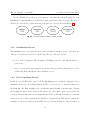
Fig. 2.1: equivalent model of meander line sections
Ls =
µ
0.2384λ
0.2384λ(ln(4
− 1))
π
d
(2.1)
Where d is the diameter of the radiator of the antenna and λ is the required resonant wavelength, the resonant frequency of the antenna can be estimated using an inductor circuit model
representation as introduced in Figure 2.1. To determine the inductance in each meandered section,
we will use an equivalent transmission line model which has a characteristic impedance given as
Z0 = 276log(
2s
)
d
(2.2)
where s is the spacing between each meandered section, as a result, the equivalent inductance
of each section, Lm, is given as following:
Lm =
|Z0 tanh(γl)|
ω
(2.3)
Where is the propagation factor of free space, l is the length of each meandered section and is
angular velocity, the resonant frequency of the meandered line antenna should have same physical
length as the simple straight line monopole antenna, but we need to replace the equivalent inductor
Ls by the sum of Ls+NLm, where N is the number of meander sections.
In order to exam the resonant behavior of the meandered line antenna, we will simulate and use
optimism method in HFSS to compare each group of meandered antenna parameters given above.
M0 to M5 configurations shown in Figure 2.2 (Best, Morrow) is applied to observe the variation
the resonant frequency of the antenna [2][3].
The M0 configuration has a self-resonant frequency at 80MHz, while the M5 configuration
5
Microwave Imaging of a Grain Bin
2.1 E-field Antenna
Fig. 2.2: meandered monopole antenna geometry
has a self-resonant frequency at 110MHz. For antenna represented in 2.1, s is equal to 1cm, L is
equal to 4cm, using equation (2.2) and (2.3), and the value of Lm is calculated as about 300nH, a
comparison table of resonant behavior of different numbers of section is listed in Figure 2.3.
Fig. 2.3: Resonant frequency of meandered line antenna M0 to M5
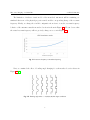
From Figure 2.3, it is evident that the inductor circuit model representing the meandered
antenna provides an acceptable prediction showing a liner increase in resonant frequency as a
function of increasing bending sections, however, in the real case, the resonant frequency of the
meander line antenna will not linearly increase with the number of sections [2][3].
6
Microwave Imaging of a Grain Bin
2.1 E-field Antenna
The limitation of inductor circuit model of the meandered antenna is still in examining, we
simulated that some of the physical properties varied and the corresponding change of the resonant
frequency. Firstly, we change the s in M1 configuration from 1cm to 2cm, the resonant frequency
behavior of the antenna versus the meandered sections is shown in Figure 2.4. We can observe that
the actual resonant frequency will not precisely change as we seen in Figure 2.3.
Fig. 2.4: resonant frequency vs meandered spacing
Next, we examined the effect of bending angle changing for each meandered section shown in
Figure 2.5 [2]
Fig. 2.5: Bending angle when α= 45,60,75,90,120 degree conditions
7
Microwave Imaging of a Grain Bin
2.1 E-field Antenna
We bend the antenna for the configuration M5 too see the simulation results in HFSS while
keep the total physical length and spacing as the same as the previous model. The relation between
bending angle and self-resonant frequency is shown in Figure 2.6 [1].
Fig. 2.6: the relation between bending angle and resonant frequency
Fig. 2.7: radiation principle of a 90 degree bending meandered antenna
8
Microwave Imaging of a Grain Bin
2.1 E-field Antenna
It is observed that resonant frequency would experience a little fluctuate when the bending angle
is changing from 45 to 120 degrees. Nevertheless, we need to obtain a relatively large difference
between cross-plane and co-plane polarization, as we can see in Figure 2.7, the 90 degree bending
angle will provide a cancellation of radiation in horizontal axis due to the opposite flowing direction
of two current. At the same time, the radiation current will always along a same direction in
vertical axis, as a result, the radiation of the 90 degree bending antenna is equivalent to a single
line monopole antenna. Furthermore, the 90 degrees bending method will save room on PCB board
so that the total physical length of the antenna will get dropped [1].
2.1.2
Antenna Building and Testing
After investigating the effects of numbers of section, section spacing and bending angle, we start to
build a meandered antenna on the substrate to satisfy the specification of the antenna parameters.
As seen in Figure 2.8, the spacing between each meandered section is 0.5cm, the number of meandered sections is 14 in total, and the S11 graph is shown in Figure 2.9 which provide us a return
loss below -10dB at 80MHz.
Fig. 2.8: final antenna view
9
Microwave Imaging of a Grain Bin
2.1 E-field Antenna
The physical length of this antenna is 80cm in total with the height of 10cm on the substrate,
a top loading cap is added at the far end of the antenna to increase the S11 performance. To match
up the resonant circuit, we add a 400nH inductor at the feeding point of the antenna. When testing
the S12 parameter, we used a λ/4 dipole antenna as port 2 in HFSS so that the designed antenna
is acting as a receiving antenna in the air box. The simulation model is shown in Figure 2.9. And
the simulation results are listed in Figures 2.10, 2.11 and 2.12.
Fig. 2.9: S11 curve for meandered antenna in HFSS
In the real testing, the resonant frequency got shifted to 95MHz due to the inaccurate selection
of the inductor value, since we can only get 330nH or 470nH one from the lab, the result frequency
will not located in 80MHz.
10
Microwave Imaging of a Grain Bin
2.1 E-field Antenna
Fig. 2.10: S11 curve for real testing results
Fig. 2.11: S12 curve for cross-plane polarization in HFSS
11
Microwave Imaging of a Grain Bin
2.1 E-field Antenna
Fig. 2.12: S12 curve for co-plane polarization in HFSS
12
Microwave Imaging of a Grain Bin
2.1 E-field Antenna
Fig. 2.13: S12 for cross-plane polarization in real test
Fig. 2.14: S12 for co-plane polarization in real test
13
Microwave Imaging of a Grain Bin
2.2 H-field Antenna
As a conclusion, for S12 curves shown in Figures 2.13 and 2.14, in HFSS the results is pretty
good that difference between co-plane and cross-plane of S12 is about 15dB, but in the real test,
the difference is 5db, the cause for the difference in quantity is from the non-ideal air box and
ground plane from the lab comparing to the ideal ones in HFSS. Further improvement for the
testing method is still required.
2.2
2.2.1
H-field Antenna
Purpose
Normally microwave imaging systems consist of a simple E-field antenna such and a monopole or a
dipole antenna which has one polarization and it is limited in its functionality, however it is simple
to model in the imaging inversion algorithm as these types of antennas have very simple and well
defined current distributions along them. Due to a grain storage bin being round, metallic, and
closed off at both ends, it can be thought of as a cylindrical resonant chamber which introduces a
level of difficulty in designing antennas that can operate in such an environment. However since the
walls of the bin are metallic, the field components at the metallic walls are easily differentiable, the
H-fields are tangential to the metallic walls of the chamber, and the E-fields are perpendicular to
the walls, thus we would like to have an antenna that is capable of probing the tangential H-fields
only.
The H- field antenna design had to be confined to the following design criteria in order for it
to be effective inside of the grain bin:
1. Ability to pick up H-field only, and reject most of the E-field
2. Minimal size (less that 15cm in length or witdth)
3. Frequency of operation between 70Mhz-90Mhz
4. Matched to 50 ohm coaxial transmission line
14
Microwave Imaging of a Grain Bin
2.2 H-field Antenna
5. Physically able to withstand grain being filled into the bin
6. Reduced complexity(for ease of modeling in the inversion algorithm)
7. Ease of manufacturing and reproduction
2.2.2
Research
The typical design procedure for an H-field antenna is a loop of perimeter one λ as at that length
the loop becomes purely resistive with the maximum amount of radiation resistance, however this
approach does not work for the grain bin as the perimeter of the loop would have to be almost 4
meters.
The other typical approach to designing h-field antennas is to decrease the perimeter of the
loop and increase the number of turns which allows for the required size reduction that we are
looking for as well as enable it to be matched to a 50ohm coaxial line since the radiation resistance
S 2
is proportional to the number of turns squared Rr = ( 177N
λ ) , however it is also not feasible for
the grain bin since it would not guarantee that the antenna does not pick up the E-field as well,
and it would be too complex to model in the imaging software.
2.2.3
Design
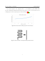
In order to satisfy the main requirement of the antenna (1) a shielded and slotted loop antenna
was chosen, which is a common type of antenna used in radio.
The ground layer around the conductor which acts as the shielding modifies the electric field
distribution inside of the antennas cross sectional area due to the boundary conditions on a PEC,
thus reducing its effect on the antenna, this effect is confirmed in the simulation results in section
2.2.6. Since the magnetic field passing through the loop induces a current on both the conductor
and the shielding, a slot is cut out in the shield to create a capacitance which introduces a phase
shift between the two currents and therefore there is a difference in potential across the load [5].
The second requirement (2) was met by reducing the perimeter of the antenna to λ/20, how15
Microwave Imaging of a Grain Bin
2.2 H-field Antenna
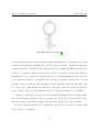
Fig. 2.15: shielded loop antenna [4]
ever the small size presented another challenge which is matching the loop antenna to the 50ohm
coaxial line, different ways of matching were considered such as capacitive coupling and transformer
coupling between the coaxial line and the antenna, These were simulated in HFSS but found the it
would be too complex to build accurately, and it would not be feasible to mount in the grain bin.
Mohammad (Project co-supervisor) suggested the use of a 50ohm termination at the end of the
loop to match the antenna to a 50ohm line and to cut the loop in half so that the size of it could
be further reduced as well as to take advantage of having a metallic wall as the other half of the
loop. A prototype of this antenna was built using a semi rigid coaxial cable with a slot cut in the
ground conductor and a 50 ohm termination was used to match the antenna to a coaxial line.
A difference of 10db was observed between the E and H polarization. However building multiples of such antennas accurately would not be feasible since the slot size would vary and produce
inaccurate results as well as the curvature in the antenna is tough to reproduce accurately.
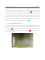
In order to make the antenna easy to manufacture and reproduce, it was decided that a PCB
version would be best suitable.
16
Microwave Imaging of a Grain Bin
2.2 H-field Antenna
Fig. 2.16: prototype antenna
2.2.4
PCB Antenna Design
To achieve a shielded coaxial line on PCB, a groundless co-planar waveguide was chosen, due
to material availability, 0.8mm FR-4 material was chosen as the PCB material with a relative
permittivity of 4.3. Due to the limited capabilities of the PCB prototyping machine available at
the EIL lab, a minimum cut in the PCB could not exceed 0.2mm, therefore 0.2mm was chosen
as the gap between the conductor and the ground planes of the co-planar waveguide. With the
help of TX-line (transmission line calculation software) a conductor size of 2.57mm with a gap of
0.2mm and a 0.8mm FR-4 thickness yields the necessary 50ohm transmission line. The size of the
antenna is 12.5cm in length and 5.5cm in width with 45 degree bends for reducing reflections, the
bent sections are 1cm long.
2.2.5
PCB Antenna Simulation
The PCB version of the antenna is constructed in the high frequency structure simulator with FR-4
as the substrate material, copper material on top of the substrate is simulated as perfect conductor
and an infinite ground plane as the antennas backing plate. The design is simulated and optimized
to obtain its performance characteristics. From optimization a slot size of 1 mm is chosen in the
17
Microwave Imaging of a Grain Bin
2.2 H-field Antenna
shielding.
Fig. 2.17: HFSS model of PCB antenna
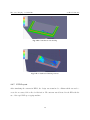
2.2.6
Simulation Results
The desired result is to have an S11 (insertion loss) of -10db at the frequency of operation, and
as expected the insertion loss at 80 MHz is -14.5db as well as due to the 50 ohm termination the
antenna has a really high bandwidth.
The simulation also confirms the effect of the co-planar ground plane on the Electric fields inside
the cross sectional area of the antenna, Figure 6 and Figure 7 show the antenna with shielding and
antenna without shielding E-field magnitude distribution in the cross sectional area.
18
Microwave Imaging of a Grain Bin
2.2 H-field Antenna
Fig. 2.18: S11 simulated
Fig. 2.19: S11 of actual antenna
19
Microwave Imaging of a Grain Bin
2.2 H-field Antenna
Fig. 2.20: E distribution with shielding
Fig. 2.21: E distribution Shielding removed
2.2.7
PCB Layout
After simulating the antenna in HFSS, the design was transferred to Altium which was used to
create the necessary Gerber files for fabrication. The antenna was fabricated in the EIL with the
use of the rapid PCB prototyping machine.
20
Microwave Imaging of a Grain Bin
2.2 H-field Antenna
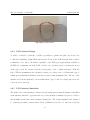
Fig. 2.22: fabricated antenna
2.2.8
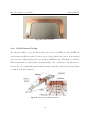
H-field Antenna Testing
The antenna’s ability to reject the Electric field was tested in a G-TEM cell. The G-TEM cell
creates transverse EM waves guided between a pair of plates with H orthogonal to E, the incident
wave was created with a signal generator producing an 80 MHz sine wave with 0dbm power and the
AUT measurements were taken with a spectrum analyzer. Two orientations of the antenna were
tested in the cell, longitudinally parallel with the magnetic field (E-orientation) and perpendicular
to magnetic field (H-orientation).
Fig. 2.23: field lines in G-TEM for reference
21
Microwave Imaging of a Grain Bin
2.2.9
2.2 H-field Antenna
G-TEM Test Results
The noise floor of the antenna was measured at -83dbm with incident power of -13dbm.
When oriented in the E-orientation the antenna received -81dbm which is close to the noise
level of the antenna, when oriented in the H-orientation the antenna received -65dbm therefore a
difference of 16db exists between the two orientations which shows that the antenna is picking up
only H-field.
Fig. 2.24: E-orientation
22
Microwave Imaging of a Grain Bin
2.2 H-field Antenna
Fig. 2.25: H-orientation
23
Microwave Imaging of a Grain Bin
Chapter 3
Multiplexer
The multiplexer consists of two sections; an RF switch section and a DC switch section. The RF
switch provides a path for the signal to and from the VNA to the antennas, while the DC switch
provides the logic necessary to set the correct path in the RF switch at the correct time. In order
to collect the data required to create an image of the grain bins contents, an array of antennas
needs to be connected to the VNA. Figure 3.1 shows how the multiplexer connects the VNA to the
array of antennas. The VNA has two ports, one which transmits a signal and one which receives
a signal. Through commands sent from the DC switch, the multiplexer is capable of connecting
either of these two ports to any of the antennas in the array.
3.1
RF Switch
3.1.1
Background
The multiplexer must connect the ports from the VNA in a certain sequence. First, the multiplexer
will be configured to connect the transmitter port from the VNA to antenna 1. After this, antenna
2 will be connected to the receiver port of the VNA. Then antenna 3 connects to the receiver
port, then antenna 4 and so on through the entire array of antennas. Once this sequence has been
24
Microwave Imaging of a Grain Bin
3.1 RF Switch
completed the multiplexer will now be configured to connect the transmitter port of the VNA to
antenna 2, after which antenna 1 will be connected to the receiver port, then antenna 3, then
antenna 4 and so on through the entire array again. The multiplexer will repeat this sequence until
all antennas have acted as the transmitter with the remaining antennas acting as receivers.
Fig. 3.1: Multiplexer connecting VNA to antenna array
3.1.2
Design
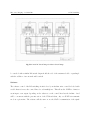
An initial design for the RF multiplexer was created using six 4 x 2 matrix switches together two
SP3Ts. The topology of this design is shown in Figure 3.2. Note that not all of the 4 x 2 matrix
switches are shown in the Figure, 4 more of these switches are connected to the two remaining pins
of the two SP3Ts for a total of 24 antennas. The 4 x 2 matrix switch chosen for this design was
from Hittite Microwave Corporation, part number HMC596LP4 and the SP3Ts chosen were part
number HMC245QS16 also from Hittite Microwave Corporation. This design was chosen for its
simplicity which would allow for good performance.
However, we were not able to use this design, as it was realized that the 4 x 2 matrix switches
chosen do not operate in the frequency range needed for our project of 70 - 90 MHz. More research
25
Microwave Imaging of a Grain Bin
3.1 RF Switch
was done but no switches of this type were found that operate in the required frequency range
for this project. Due to this limitation a new design was chosen consisting of a series of cascaded
RF switches, including SPDTs, SP3Ts and SP8Ts. The topology of this design is shown in Figure
3.3. The switches used in this design are HMC349MS8G, HMC245QS16 and HMC253QS24 from
Hittite Microwave Corporation.
Fig. 3.2: Initial design of the multiplexer
With this design decided on, we needed to get it manufactured on PCB. To create the PCB
layout necessary to get these boards printed, software package Altium was used. Two boards were
designed for the RF portion of the multiplexer; one containing only an SP3T and one containing
two SP8Ts and eight SPDTs. The final 2 x 24 multiplexer requires two of the boards with SP3Ts
and three of the boards with SP8Ts and SPDTs. The final PCB layout of the two boards is shown
in figures 3.4, 3.5 and 3.6.
26
Microwave Imaging of a Grain Bin
3.1 RF Switch
Fig. 3.3: Final design of the multiplexer
Fig. 3.4: PCB layout for SP3T board
27
Microwave Imaging of a Grain Bin
3.1 RF Switch
Fig. 3.5: PCB layout for top layer of SP8T and SPDT board
Both boards were designed with 4 layers using a substrate of FR-4. The stack up of the boards
consists of a top signal layer, followed by a substrate layer, then an internal signal layer (used only
as ground in this design) and then the prepreg layer. Below the prepreg layer is a mirror of what
is on top of it; an internal signal layer, then substrate layer and then bottom layer. The stack up
from Altium is shown in Figure 3.7.
28
Microwave Imaging of a Grain Bin
3.1 RF Switch
Fig. 3.6: PCB layout for bottom layer of SP8T and SPDT board
Fig. 3.7: Stack up for PCBs in Altium
29
Microwave Imaging of a Grain Bin
3.1 RF Switch
Both boards used co-planar waveguides with ground for all of the RF traces and were designed
such that they were 50 ohms. This resulted in a trace width of 0.5 mm and a gap of 0.115 mm with
a substrate thickness of 0.6 mm. Three 10 pin connectors were added to provide power as well as
connect all of the control pins for the SP8T and SPDT switches [6].
Unfortunately, due to issues with our original intended supplier of our PCBs, we were unable
to get these PCBs printed in time for this report. We found another supplier for our PCBs and
hope to have them before our presentation. The PCBs needed to be modified somewhat due to
different PCB specifications from this new supplier. Minimum routing size was larger at 0.1524
mm compared to 0.1 mm with the original supplier. Also, the substrate thickness options were
different, not allowing us to use a thickness of 0.6 mm. Based on the specifications of the new
supplier the RF traces needed to be modified to 0.185 mm thick with a gap of 0.1524 mm. This is
based on a substrate thickness of 0.1 mm.
30
Microwave Imaging of a Grain Bin
3.2
3.2 DC Switching
DC Switching
A DC switch used in combination with and RF switches reduces the total labor and cost of having
a separate pathways for each antenna. This therefore enhances the portability of the design and
reduces the complexity of very expensive PCBs. due to the cheaper cost in comparison to their RF
counterparts and the reduction in frequency interference due to the maximum attenuation of any
frequency components at DC. For our design we need a DC circuit for address decoding of the RF
switch. In effect, the function of the DC switch is to set the control parameters in order to specify
what the response of the RF switch will be at that point in time.
At the onset of the project, we examined the previous switch design to understand how it
would integrate with the RF switch and set the control parameters for the acquisition of data by
the VNA. Our goal was to improve upon this design so that it was feasible with the new system
we wanted to implement.
The design of the switch required the use of Altium and the Arduino user interface. The
hardware was designed in Altium and the software was writing in the Arduino mainframe in the
C++ programming language
3.2.1
Hardware
The initial design appeared very complex and cumbersome to deduce because it had wires everywhere. The first task was therefore to ascertain the possibility of having a neater hardware with
very minimal adjustment to the circuit after the printing of the PCB. This meant that most of the
design should be implemented in the PCB in order to reduce complexity and make troubleshooting
easier. This also ensure a reduction in noise cause by all the numerous wiring and addition electrical
components that was everywhere.
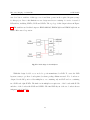
Figure 3.8 highlights that function of the DC switch in perfect simplicity. The control parameters are letters from A to L and these are sourced from the DC switch to the SP3Ts, SP3Ts and
SPDTs of the RF switch
31
Microwave Imaging of a Grain Bin
3.2 DC Switching
Fig. 3.8: Topology for the integration between DC and RF Switches
Designing the PCB first started with the schematic and a review of the schematic to ensure its
accuracy. Figure 3.9 is the initial schematic that was used in the printing of the PCB in Altium.
This was designed to be efficient and less complicated however, the simplicity brought about some
complication when it was being integrated with the RF Switch.
Using an Arduino board, the previous schematic was put to the test. It proved to work in
every sense of the word without any glitches. It carefully selected that right control parameters
and turned the respective led pins on which meant theoretically, we had a good hardware and
software.
The simplicity of the first designed was questioned when the second version of the RF switch
design was completed and had a similar schematic design as the previous design. This implied that
the new improvements made to the design, which was based on using a 4x2 matrix switch, was
not going to be feasible with the original schematic and a more complex design is shown in Figure
3.10 had to be implemented. It is definitely more rigorous that the first but had however proved
to be better. It this sense, the DC switch supports a multilayer RF switch design and can feasible
32
Microwave Imaging of a Grain Bin
3.2 DC Switching
Fig. 3.9: Initial DC Switch Design for Matrix Switch Design
be cascaded with a similar DC switch design should the side of the antennas double or quadruple
with the addition of an external enable switch.
Software
The software control of the DC switching circuit is done by an Arduino microcontroller loaded with
a table that references the control lines for each multiplexer. This allows the SPDTs to function
as an input or an output depending on the values set on the control lines but the Arduino. And
will be concurrent with the presents action of the VNA such that, only one SPDT is in transmit
mode at a given time. The software will also turn on one the SP8T for transmission of the signal
33
Microwave Imaging of a Grain Bin
3.2 DC Switching
Fig. 3.10: Final DC Switch Design for Multi-Layer RF Switch Design
and turn the other SP8Ts responsible for reception of the signals.
After the research and understanding of requirements were satisfied, a truth table was drawn in
order to simplify the circuit to its least possible scenario where the fewest components are used to
achieve the expected results. This truth table was then transcribed into code for and then loaded
unto the Arduino. This Arduino was set to function in synchronism with the Raspberry Pi.
The pins to be used for the DC circuit had to be chosen in such a way that they match the
truth table shown in Appendix D. The Arduino code was then written to first store the truth
table in memory and query the table with instructions when needed. The row will be traversed and
parameters set according to the value stores in that position of the array referencing an Arduino pin.
34
Microwave Imaging of a Grain Bin
3.2 DC Switching
This was an improvement on existing software which use a number of arrays to store the information
and therefore introduced some time delay when looping through these arrays. The software was
loaded unto the Arduino and tested with LED lights to show its effectiveness in selecting the right
layer and facilitation the transmission and reception of signals. Our initial design required such
a table for address decoding of the switch however, dues to design change, the code was modified
to attempt to address decode single pole ICs. The intention was to leave it as a table for future
improvements however, with time, it was realized that it made the code slower than expected and
could easily pose problems for anyone who was not familiar with using multidimensional tables.
The software was enhanced and improved by first by connecting the Arduino to a breadboard
and sending it the initial start instruction. And observing on the board that the right control
parameters was being set for the RF switch via the automated Arduino function. The goal of
the software side of our project is to get the Raspberry Pi to send a specific number which would
correspond to one of the antennas and this will be used for transmission of the signal. This
would cause the the Arduino will set the parameters for transmission via that antennae and would
be followed by a series of code setting the parameters from the reception of the signal via the
remaining twenty-three antennas. Thus after one transmission via serial input, the Arduino would
receive twenty-three reflected signals via serial without having to call the send any loops for the
receiving signal.
A few scenarios posed during our troubleshooting sessions brought about the need for this more
robust code to be written to the Arduino. Firstly, we were going to be use our devices on farm and
chances are, the farmers will not have the expertise to trouble shoo when something goes wrong.
There were different implementable codes written to address these potential issues. However, the
synchronization between the Arduino software and the Raspberry Pi made this almost impossible
to accomplish.
It was considered that either the Raspberry software of the Arduino software should be capable
of automated function once the start button is push or a signal is sent to a pin in order to make
35
Microwave Imaging of a Grain Bin
3.2 DC Switching
starting the data acquisition and stopping the running routine easily understood to the average
farmer.
3.2.2
ESD Protection
Any reliable system design requires some form of Electrostatic Discharge protection. Choosing the
right circuit protection device involves considering criteria such as: Response time, ESD current
handling capacity and, maximum reverse leakage current. Also the device should not interfere with
the normal operation of the circuit. Designing the DC circuit also meant taking the RF circuit into
consideration in order to minimize electrostatic discharge and current leakage.
We considered N-well resisters, gate-grounded and gate-coupled protection options, silicon controlled rectifiers and diodes. Ultimately we decided to use diodes and capacitors due to its simplicity.
During our design phase, the options available were to implement ESD protection on the
antenna or on the switch box. We chose to go with ESD protection for the switch box because it
was less expensive to do it that was and it was a trusted and proven route to for to ensure that a
great amount of ESD is dealt with in our circuit.
There is no addition intended for the ESD protection. The data sheet and simulations we run
serves to hold that our diodes will work well within our range of interest
36
Microwave Imaging of a Grain Bin
Chapter 4
Vector Network Analyzer
The vector network analyzer is a key component of the S-Parameter Data Acquisition (SPDAQ)
system since it is the actual instrument that measures the S-Parameters of the grain storage unit.
4.1
Harware Specifications
In order to implement a practical system that would be ideally used by agriculturalists such as
farmers, the VNA had to be portable yet affordable. Lab quality VNAs are very expensive, usually
costing tens of thousands of dollars, and therefore cannot be used for the SPDAQ system. Due
to the fairly low frequencies being transmitted and received from the antennas within the grain
storage unit, the VNA can be more affordable than those usually found in a lab. On top of these
main specifications of a compact, low-costing VNA, the analyzer had to be a two port system so
it is capable of S11 and S12 measurements for the microwave imaging of the grain bin,as well as
being capable of measuring within the frequency range of a typical grain bin,and can offer a good
dynamic range. Table 4.I shows the exact specifications required for the SPDAQ system to be
effective.
37
Microwave Imaging of a Grain Bin
4.1 Harware Specifications
Table 4.I: VNA Requirements [7]
Frequency Range
Dynamic Range
System Type
Budget
70 MHz - 100 MHz
10 dB
2-port with S11 and S12
<$1000
These criteria help facilitate in the decision of selecting the MiniVNA Pro (MVP) by Mini
Radio Solutions which offers a more affordable and portable solution for the VNA component of
the SPDAQ system.
Table 4.II: miniVNA PRO Specifications
Frequency Range
Dynamic Range
System Type
Cost
0.1 MHz - 200 MHz
90 dB in Transmission mode
50 dB in Reflection mode
2-port with S11 and S12
$549.95 + taxes and fees
As shown in Table 4.II, the MVP meets all the main VNA requirements for the SPDAQ system
which made it a valid solution for the VNA component.
38
Microwave Imaging of a Grain Bin
4.2
4.2 Calibration and Testing
Calibration and Testing
To ensure that the MVP meets our system’s standards, results measured from the MVP were
compared to the more high-tech VNAs in the Electromagnetic Imaging Lab (EIL) that are normally
used for the imaging data. The MVP is first calibrated using the calibration tool provided by the
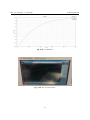
EIL and calibration files are created using the MVP software, which is shown in Figure 4.1.
Fig. 4.1: miniVNA PRO calibration software.
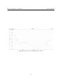
The S11 measurement of the miniVNA PRO was then compared to the S11 measurement of the
EIL VNA in order to verify the calibration was performed correctly on the miniVNA PRO. The RF
Switch module provided by the EIL was used as a load. The S11 output of the RF Switch transfer
function is shown in Figure 4.2 and 4.3 for both the EIL VNA and the miniVNA PRO. Both the
real and imaginary part of the S11 measurement are fairly similar with a slight discrepancy in
the real part of S11 in the miniVNA PRO which may be due to the calibration kit used with the
miniVNA Pro since the kit was designed for the EIL VNAs. With fairly accurate results, the MVP
39
Microwave Imaging of a Grain Bin
4.2 Calibration and Testing
S11 Real
gave us confidence in using it for the SPDAQ system.
Freq (Hz)
S11 Imaginary
Fig. 4.2: S11 measurement(real) for both VNAS.
Freq (Hz)
Fig. 4.3: miniVNA PRO open port measurement in reflection mode.
40
Microwave Imaging of a Grain Bin
4.3
4.3 miniVNA PRO Software
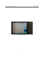
miniVNA PRO Software
The MVP was designed to be software-defined and the manufacturer did not have any indications
that they will make this device open source. This forced our team to go ahead with the manufacturer’s software in order to use the MVP despite the slow read times of each measurement.
Fig. 4.4: miniVNA PRO Software Output
The MVPs software used for the SPDAQ system is the ’vnaJ-hl.3.1.3.jar file [9] that runs on
a headless system (no graphical user interface). When the jar file is executed with the specified
parameters (frequency start, stop and steps), the MVP takes the readings and exports them to a
CSV file (the file type is specified within the parameters of the jar file). An example output of the
MVPs software running through a command line interface (CLI) is shown in Figure 4.4.
41
Microwave Imaging of a Grain Bin
Chapter 5
Microprocessor
5.1
Hardware Integration
Due to the software limitation of the MiniVNA Pro (MVP), a microprocessor was required to run
the MVPs software. This is where the Raspberry Pi 2 (RPi2) was chosen. The RPi2 microprocessor
will be used to control both the RF Multiplexer and MiniVNA Pro (MVP) of the S-Parameter Data
Acquisition (SPDAQ) system. The specifications of the RPi2 are shown in Table 5.I.
Table 5.I: Raspberry Pi 2 Specifications [8]
Processor
RAM
USB Ports
GPIO Pins
900Mhz quad-core ARM Cortex-A7 CPU
1GB
4
40
The RPi2 offers enough USB ports to connect the RF Multiplexer (RF Mux) and MVP. As
well, the RPi2 offers GPIO pins, which will be used to integrate user interface (UI) features for the
user to have better control of the system. Such UI features that were implemented with the RPi2
was a button to run the SPDAQs software when pressed and a LED indicator to allow the user
to know when the program is ready for the user to press the button. A circuit is shown in Figure
42
Microwave Imaging of a Grain Bin
5.2 Software Design and Integration
5.1 that displays the button and LED connection to the appropriate GPIO pins on the RPi2 (see
Appendix C for Raspberry Pi 2 Pinout Configuration).
Fig. 5.1: LED and Button Circuit
Initially, the SPDAQ system was designed around the Raspberry Pi Model B+ but due to the
new release of the RPi2 in February, 2015, the decision to upgrade seem obvious with the faster
processor at the same low cost of $39.99 CAD + shipping that the old Raspberry Pi Model B+
was priced at. The hardware upgrade helped greatly improve the software run times down to 16s
per measurement to 5s per measurement. Boot up times for the system also greatly reduced to 6s
from 15s.
5.2
Software Design and Integration
Arch Linux was installed onto the RPi2 due to its minimal architecture. It is a lightweight operating
system (OS) that is text-based with no GUI making it very quick to boot up. Since the SPDAQ
system has no need for a GUI and the software that will be running on the RPi2 did not require
much to run, the Arch Linux OS provided a great solution for our system.
43
Microwave Imaging of a Grain Bin
5.2 Software Design and Integration
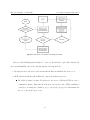
For the SPDAQ system, there are four main processes that the system is required to run:
Initialization, Data Acquisition, Post-Data Processing, and Remote Data Accessing. The order of
all these processes and procedures that run on the microprocessor are shown in Figure 5.2.
Fig. 5.2: S-Parameter Data Acquisition system processes.
5.2.1
Initialization Process
The initialization process requires the user to interact with the system to power on and start the
other processes that are executed by a shell script. The procedure is as follows:
1. Power on the S-Parameter Data Acquisition (SPDAQ) system by connecting the RPi2 to a
power source.
2. Once booted up (allow approximately 7s), the user can now press the push button to execute
a shell script that will start the data acquisition process.
5.2.2
Data Acquisition Process
In this process, the RPi2 will control both the RF Multiplexer to switch the antennas between
transmitter and receiver as well triggering the MVP to execute a sweep to obtain S-Parameters of
the Grain Bin. The Data Acquisition Process runs through an N-number antenna array collecting
the S-parameter data from the grain bin through the use of the MVP, which exports a CSV file
per sweep. Each antenna will act as a transmitter and will loop through all n number of antennas
acting as a receiver, which results in an N x N number of measurements. This will also result in N x
N number of exported data files from the MVP due to its software limitations. These data files are
44
Microwave Imaging of a Grain Bin
5.2 Software Design and Integration
exported to /root/vnaJ.3.1.3/export directory of the RPi2. A flow chart of the Data Acquisition
Process is shown in Figure 5.3 which outlines this procedure.
Fig. 5.3: Flow chart of the Data Acquisition Process.
5.2.3
Post-Data Processing
Post-Data Processing procedure is executed by the shell script after the Data Acquisition Process
is done. In this process, the exported CSV files from the MVP are reformatted to a single data file,
which the user can access for further processing such as microwave imaging analysis of the grain
bin. The exported CSV files are located in the /root/vnaJ.3.1/export directory with the filename
format of
gbin_(tx)(rx).csv
where ”(tx)” and ”(rx)” are the 2-digit transmitter and receiver antenna number, respectively,
within the array that the MVP measured from. The MVP exports the data as transmission
loss in dB and transmission phase (degrees), which is S12 in polar form, however Cartesian complex form is required for post-analysis and therefore a small calculation is required prior to writing to file. The calculations performed are described below: The MVP provides its data as so,
45
Microwave Imaging of a Grain Bin
5.2 Software Design and Integration
T ransmissionLoss(T L) = 20 log10 |S12|
T ransmissionP hase = θ
The desired data form is as so, S12 = a + bi
Variables a and b are calculated as shown,
a = |S12| cos θ
b = |S12| sin θ
where, |S12| = 10(T L/20)
Once the S12 data is calculated to Cartesian complex format, it is then written to a file called
sp.dat which is located in /root/grainbin/output/ directory. The format of the file is shown as:
Tx Rx Probe
S12 Real S12 Imaginary (repeating for all frequency steps)
Where Tx is the transmitter antenna number and Rx is the receiver antenna number, which is
then followed by the S12 real and imaginary data in succession for all 100 frequency steps. A flow
chart of the Post-Data Processing procedure is shown in Figure 5.4.
5.2.4
Data Transmission Process
The sp.dat file contains all of the S-parameters of the grain storage unit and this file will be
accessible to the user through the cloud if an Internet connection is present. The shell script will
execute the data upload process after the Post-Data Processing is complete in which it executes a
command in Linux that triggers an upload of the specific file to Dropbox.
Dropbox is a widely used cloud storage service that anyone can register for free for basic cloud
storage space. This service can be accessed online remotely from the users own PC through the
many interfaces that Dropbox offers (ex. website, computer software, etc.), which makes it very
convenient for the user to retrieve the data from the SPDAQ device and therefore was selected for
our system. Appendix B.4 instructs how a user can unlink or link a specific Dropbox account onto
the RPi2 as well as additional commands.
46
Microwave Imaging of a Grain Bin
5.2 Software Design and Integration
Fig. 5.4: Flow Chart of Post-Data Processing Procedure.
However, if the SPDAQ system is unable to connect to the Internet to upload the data file, the
user can still manually retrieve the data through the following methods:
1. Ejecting the micro-SD card located underneath the RPi2 in which the file is stored on.
2. SFTP with the RPi2 through an Ethernet connection with another device.
The RPi2 is assigned a static IP address for the user to SSH and SFTP in order to
communicate with it. That static IP address is: 192.168.2.23. Once SFTP establishes a
connection, executing the command, get /root/grainbin/output/sp.dat will transfer the
file over to the users remote device.
47
Microwave Imaging of a Grain Bin
5.3
5.3 Software Setup and Configuration
Software Setup and Configuration
This chapter section details the software setup and configuration on the RPi2 to run the SPDAQ
software. The purpose of this section is to help a user recreate the SPDAQ software on the RPi2
in the case of any software error or corruption or to simply modify specific software parameters to
tailor to the user’s needs.
5.3.1
Prerequisites
The RPi2 is setup with a username and password. The default login information for Arch Linux is
the following:
Username: root
Password: root
However for security purposes, the password was changed to ’gbin2015’ with the same username.
In order for the RPi2 software processes to function, certain files need to be included on the RPi2
stored in the directory /root/grainbin. A list of these files is shown in Table 5.II
Table 5.II: Required files in the /root/grainbin directory of the Raspberry Pi 2.
File
vnaJ-hl.3.1.3.jar
gbin.sh
dropbox-uploader.sh
put2str.exe
button.py
Description
miniVNA PRO headless software
shell script t run all of the SPDAQ processes (see Appendix B.1)
Dropbox shell script to upload ”sp.dat” file to a linked Dropbox account on the RPi2 (see Appendix B.4)
processes the exported CSV files from the miniVNA PRO (see Appendix B.2)
button and LED function on the Raspberry Pi 2 (see Appendix C)
Specific packages also need to be installed onto the RPi2 for the files to run properly on the
Arch Linux OS. The following commands shown in Table 5.III can be executed on the RPi2 terminal
with Arch Linux installed. Ensure that the RPi2 is connected to the Internet in order to download
these packages.
Once the packages are installed, the MVP’s software requires specific directories to be created.
These directories are created when the ’vnaJ-hl.3.1.3.jar file is executed for the first time which can
48
Microwave Imaging of a Grain Bin
5.3 Software Setup and Configuration
Table 5.III: Required packages to be installed on Arch Linux OS running on the Raspberry Pi 2.
Command
pacman S jdk7-openjdk
pacman S mono
pacman S python-raspberry-gpio
Description
Java package
C# Compiler
Raspberry Pi GPIO Python library
be executed using the following command:
java Dconfigfile=gbin.xml -Dfstart=70000000 -Dfstop=100000000 -Dfsteps=100 Dcalfile=gbin.cal -Dscanmode=TRAN -Dexports=csv -jar vnaJ-hl.3.1.3.jar
An error will occur due to certain files missing when the command is executed for the first time
however the necessary directories will be created on the /root directory of the RPi2 which includes:
/root/vnaJ.3.1/export
/root/vnaJ.3.1/calibration
/root/vnaJ.3.1/config
There are two key files that need to be present for the ’vnaJ-hl.3.1.3.jar file to execute properly.
The first one is the configuration file ”gbin.xml” (refer to the vnaJ software manual on how to create
this file [9]). The XML file includes the USB port name for the software to communicate with the
MVP. This file must be stored in the /root/vnaJ.3.1/config directory. The second key file is the
calibration file for transmission mode which are created using the ’vnaJ.3.1.3.jar GUI software that
must be run on a separate computer that supports either Mac OS or Windows. The user should
consult the vnaJ software user manual [9] for details on how these calibration files are created using
the ’vnaJ.3.1.3.jar GUI. This calibration file is stored in the /root/vnaJ.3.1/config directory.
The RPi2 is now setup to run the ’gbin.sh’ shell script that runs the SPDAQ software. In order to
use the button and LED feature, the python script ’button.py’ needs to be executed. The simple
command ”Python button.py” will run the python script and will listen for the user to press a
button to initiate the ’gbin.sh script. In order to setup the python script ’button.py at bootup, the
following command can be entered on the terminal of the RPi2:
49
Microwave Imaging of a Grain Bin
5.3 Software Setup and Configuration
crontab e
A file will come up and in this file enter in the line at the very bottom:
@reboot python /root/grainbin/button.py
Save the file and now the RPi2 will run the python script at bootup, enabling the button and LED
function. To connect the LED and push button to the RPi2, review Figure 5.1 and Appendix C
for GPIO pinout on the RPi2.
5.3.2
Configuration Parameters
’gbin.sh Parameters
The ’gbin.sh’ shell script file is designed to take four parameters that define the number of transmitters and receivers being used with the SPDAQ system. The command to run the ’gbin.sh’ file
through the RPi2 terminal is:
sh gbin.sh {1} {2} {3} {4}
The four parameters are defined in Table 5.IV.
Table 5.IV: Parameter definitions for ’gbin.sh’.
Parameter
{1}
{2}
{3}
{4}
Description
transmitter antenna start number
transmitter antenna stop number
receiver antenna start number
receiver antenna stop number
An example of this command when using transmitter antennas 1-10 and antennas 11-20 as
receiving,
sh gbin.sh 01 10 11 20
50
Microwave Imaging of a Grain Bin
5.3 Software Setup and Configuration
miniVNA PRO Software Parameters
The MVP software is executed within the ’gbin.sh’ shell script (refer to Appendix B.1) and the
parameters can be changed by changing the following command within that script:
java Dconfigfile=gbin.xml -Dfstart={Start} -Dfstop={Stop} -Dfsteps={Steps}
-Dcalfile=gbin.cal -Dscanmode=TRAN -Dexports=csv -jar vnaJ-hl.3.1.3.jar
Where the following parameters are defined in Table 5.V.
Table 5.V: Parameter definitions for miniVNA PRO software command.
Parameter
{Start}
{Stop}
{Steps}
Description
Frequency range start (Hz)
Frequency range stop (Hz)
Number of Frequency steps
The command is set within the shell script by default as:
java Dconfigfile=gbin.xml -Dfstart=70000000 -Dfstop=100000000 -Dfsteps= 100
-Dcalfile=gbin.cal -Dscanmode=TRAN -Dexports=csv -jar vnaJ-hl.3.1.3.jar
Where the frequency range is 70-100MHz with 100 steps. The user can refer to the vnaJ Headless
Software Manual [10] for additional information.
51
Microwave Imaging of a Grain Bin
Chapter 6
Future Work
At the moment, the SPDAQ system is at an early stage of development. Our team has developed
an Alpha prototype of the SPDAQ system for hardware and software testing in order to establish
a proof of concept for this project. Although our team was successful in integrating the many
hardware and software components for the system, there are still many things that can be improved
on to make the system accessible to the general public. Initial designs for the SPDAQ system was
to implement a battery operated device however due to project time constraints and project delays,
this feature has yet to be implemented but should considered for future iterations. This chapter will
explain the possible work that can be done to advance the current alpha prototype of the SPDAQ
system and its individual components.
6.1
Software
As of now, the current software is at its very basic form where a shell script executes the SPDAQ
software on the RPi2 with very little interface for the user to interact with. The user can edit
certain files on the RPi2 in order to modify the settings which requires root access to the RPi2.
This current method requires a good knowledge of the LINUX OS which is not commonly known
by the average user. By implementing a more advanced GUI, the user can have more control over
52
Microwave Imaging of a Grain Bin
6.2 RF Multiplexer Module
the SPDAQ system with an easier method to setup and configure any of the settings of the SPDAQ
software. The GUI can also offer an easier method for the user to connect the RPi2 to the Internet
for cloud services with a use of a Wifi adapter. To improve the software runtime, the use of another
VNA that is open source should be considered in newer iterations of the SPDAQ system.
6.2
RF Multiplexer Module
At this stage, the RF Multiplexer component is currently being built and has yet to be tested.
Through our SPDAQ prototype testing, we used an old RF Switch module provided by the EIL
for the Alpha build. The RF Mux module designed by our team offers the same logistics as the
RF Switch module provided by the EIL and therefore the upgrade to the newly designed RF Mux
model, once manufactured, should be a simple transition. The work to be done once our RF Mux
PCBs arrive will be to solder the RF switch integrated circuits (ICs) and to test with the rest of
the SPDAQ Alpha prototype.
In terms of the DC switch, an addition that will simplify this automated process between
the Raspberry Pi by and the DC switch, even in the case of software failure, would be by using
a Serial Peripheral Interface (SPI) via a GPIO for the handshake process. This extended SPI
communication will create more ports for the Arduino to use as well as provide a means for the
software to not only talk to the Arduino, but also receive interrupt flags from the Arduino which
can help in auto troubleshooting should anything go wrong during the process of data acquisition.
6.3
Antennna
The H-field antennas have been designed and tested. For the future, the E-Field antenna design
will need to be modified in order to reduce cross-polarization so it can meet the SPDAQ system
standards for a grain storage unit. Once modified, further tests need to be conducted with the
antenna integrated with the SPDAQ system.
53
Microwave Imaging of a Grain Bin
Chapter 7
Conclusions
The purpose of this project was to design a portable and affordable system for detecting moisture
inside a grain bin using microwave imaging techniques. There were several different components
comprising this system. Two types of antennas were studied; H-field and E-field antennas. A
VNA was required for sending and receiving signals to and from the antennas and a multiplexer
was required in order to connect the VNA to the array of antennas and perform the necessary
switching. Also, a microprocessor and software was needed to provide control to the multiplexer
and perform data acquisition and management.
It was found that the E-field antennas designed were not suitable for real world use for this
application however the H-field antennas performed well. Due to time constraints and issues with
our original supplier for our PCBs we were unable to complete the multiplexer in time for this
report, however we hope to have something in time for our presentation. For testing our system
we used an existing switch provided by EIL. The miniVNA PRO was a very affordable option but
we were unable to get direct access to data obtained through it which resulted in our system being
very slow in running through its data acquisition procedure. If direct access to this data were
possible or a different VNA was used which allowed this direct access, our system would perform
much quicker.
54
Microwave Imaging of a Grain Bin
With a bit more work to complete with the multiplexer and resolving the issue with the
limitation of the MVP’s manufacturer software, we feel that we can succeed at creating an affordable
and portable system for detecting moisture inside a grain bin.
55
Microwave Imaging of a Grain Bin
REFERENCES
References
[1] O.-A. R. Mohassel, “Doctoral committee: Professor chen-to tai, chairman,” Ph.D. dissertation,
The University of Michigan, 1982.
[2] S. Best and J. Morrow, “Limitations of inductive circuit model representations of meander
line antennas,” in Antennas and Propagation Society International Symposium, 2003. IEEE,
vol. 1, June 2003, pp. 852–855 vol.1.
[3] K. Deng and M. Ma, “The study and implementation of meander-line antenna for an integrated
transceiver design,” 2010.
[4] P. Frost. (2015) What, if anything, makes shielded loop antennas so great at rejecting
local noise. [Online]. Available:
http://electronics.stackexchange.com/questions/70262/
what-if-anything-makes-shielded-loop-antennas-so-great-at-rejecting-local-nois
[5] R. J. Spiegel, C. A. Booth, and E. L. Bronaugh, “A radiation measuring system with potential
automotive under-hood application,” Electromagnetic Compatibility, IEEE Transactions on,
no. 2, pp. 61–69, 1983.
[6] R. Hartley. (2015) Rf / microwave pc board design and layout. [Online]. Available:
http://www.qsl.net/va3iul/
[7] mRS mini Radio Solutions. (2015) minivna pro. [Online]. Available: http://miniradiosolutions.
com/minivna-pro
[8] R. P. Foundation. (2015) Raspberry pi 2 model b. [Online]. Available:
//www.raspberrypi.org/products/raspberry-pi-2-model-b/
http:
[9] D. Krause, vna/J 3.1.4 User guide, 2015. [Online]. Available: http://download.dl2sba.com/
vnaj/manuals/UserGuide.pdf
[10] ——, vna/J 3.x User guide for headless application, 2015. [Online]. Available:
http://download.dl2sba.com/vnaj/manuals/UserGuide.headless.pdf
[11] A. Fabrizi, “Dropbox uploader,” 2014. [Online]. Available: https://github.com/andreafabrizi/
Dropbox-Uploader
56
Microwave Imaging of a Grain Bin
REFERENCES
[12] Pi.gadgetoid.com. (2014) Raspberry pi pinout - rev 2 board. [Online]. Available:
http://pi.gadgetoid.com/pinout
57
Microwave Imaging of a Grain Bin
Appendix A
Budget
58
Microwave Imaging of a Grain Bin
Table A.I: Project Budget
SYSTEM
MODULE
COMPONENT
Antenna Array
Antenna PCBs
Metallic rods
Vector Network
Analyzer (VNA)
MiniVNA Pro
RF Multiplexer
Controller
MISC.
Supplier
Part No.
296-2057-5ND
J502-ND
501-1381ND
744-1374ND
587-1113-1ND
587-1133-6ND
HMC194MS
8
HMC245QS1
6
HMC253QS2
4
45W6205
Price/Unit
Quantity
Sponsor
Estimated
Cost
Actual
Order Cost
EIL
$300.00
$0.00
1
EIL
$600.00
$0.00
$0.43
6
EIL
$2.56
$0.00
$4.12
38
EIL
$156.42
$0.00
$6.06
5
EIL
$30.30
$0.00
$9.40
6
EIL
$56.42
$0.00
$0.34
50
EIL
$16.79
$0.00
$0.16
100
EIL
$16.06
$0.00
$3.26
24
EIL
$78.24
$0.00
$4.13
2
EIL
$8.26
$0.00
$10.28
6
EIL
$61.68
$0.00
$40.21
$10/board
$6/board
1
5
5
EIL
$40.21
$0.00
EIL
$80.00
$0.00
MUX/DEMUX
Digikey
SMA board edge
Digikey
SMA board edge
Digikey
SMA-SMA cable
Digikey
cap 10nF 0805
Digikey
cap 100nF 0805
Digikey
SPDT
Digikey
SP3T
Digikey
SP8T
Digikey
Arduino
Newark
RF Multiplexer PCBs
SeeedStudio
Raspberry Pi B+
8GB microSD card
Newark
68X0156
$43.60
1
ECE
$43.60
$43.60
Raspberry Pi 2
Newark
38Y6467
$39.99
1
ECE
$39.99
$39.99
ECE
$100.00
Electrical components
(wiring, resistors,
capacitors, etc.)
Machine Time
U of M
8 hrs.
Process of
ordering.
Provided by EIL.
Provided by EIL.
Provided by EIL.
Provided by EIL.
Provided by EIL.
Provided by EIL.
Provided by EIL.
Provided by EIL.
Provided by EIL.
Provided by EIL.
Provided by EIL.
Process of
ordering.
Order placed
and received.
Order placed
and received.
$0.00
Subtotal
13% taxes
Shipping
Total
59
Order Status
ECE
$83.59
$10.87
$8
$102.46
EIL
$1446.94
$188.10
$160.11
$1795.15
Project Total
$1530.53
$198.97
$168.11
$1897.61
Microwave Imaging of a Grain Bin
Appendix B
S-Parameter Data Acquisition System
Software
B.1
gbin.sh
Code B.1: S-Parameter Data Acquisition Shell Script Software
1
2
3
4
5
6
# !/ bin / bash
if [ ! -f vnaJ - hl .3.1.3. jar ];
then
echo ERROR ! Missing vnaJ file ...
exit
fi
7
if [ -z $ ( lsusb | grep -e " Future Technology Devices " ) ];
then
10
echo ERROR ! MiniVNA Pro not connected ...
11 fi
8
9
12
if [ $# - lt 4 ];
then
15
echo ERROR ! Missing parameters ...
16
exit
17 fi
13
14
18
if [ -z $ ( lsusb | grep -e " Arduino " ) ];
then
21
echo ERROR ! Arduino not connected ...
19
20
60
Microwave Imaging of a Grain Bin
22
B.1 gbin.sh
else
echo Tx : $ 1 - $ 2
echo Rx : $ 3 - $ 4
stty -F / dev / ttyACM0 cs8 9600 ignbrk - brkint - imaxbel - opost onlcr - isig - icanon - iexten - echo - echoe - echok - echoctl echoke noflsh - ixon - crtscts - hupcl
23
24
25
26
for i in $ ( seq $ 1 $ 2 )
do
if [ " $ i " - lt 10 ];
then
echo sending 0 $ i to arduino ...
echo -n " 0 $ i " > / dev / ttyACM0
else
echo sending $ i to arduino ...
echo -n " $ i " > / dev / ttyACM0
fi
27
28
29
30
31
32
33
34
35
36
37
echo changing transmitter to $ i
38
39
for j in $ ( seq $ 3 $ 4 )
do
echo -n " $ j " > / dev / ttyACM0
echo changing reciever to $ j
40
41
42
43
44
echo Running vnaJ - hl .3.1.3. jar ...
nohup java - Dconfigfile = gbin . xml - Dfstart =70000000 Dfstop =100000000 - Dfsteps =100 - Dcalfile = gbin . cal Dscanmode = TRAN - Dexports = csv - jar vnaJ - hl .3.1.3. jar >
log . txt
path = " vnaJ .3.1/ export "
45
46
47
48
# renaming exported file for post - processing
[ " $ i " - lt 10 ] && tx = " 0 $ i " || tx = " $ i "
rcvr = $ ( expr $ j - 24)
[ " $ rcvr " - lt 10 ] && rx = " 0 $ rcvr " || rx = " $ rcvr "
mv $ { HOME }/ $ path / gbin . cal . csv / $ { HOME }/ $ path / gbin_ "
$ tx $ rx " . csv
49
50
51
52
53
done
54
done
55
56
fi
57
61
Microwave Imaging of a Grain Bin
B.2 put2str.cs
# running post - processing process
59 mono put2str . exe
58
60
61
62
# delete all exported miniVNA files after post - processing is done
rm -R $ { HOME }/ $ path /*
63
64
65
# upload to linked dropbox
./ dropbox_uploader . sh / root / grainbin / output output
B.2
put2str.cs
Code B.2: Post-Data Processing Program
using
using
3 using
4 using
1
2
System . Linq ;
System . IO ;
System . Collections ;
System . Collections . Generic ;
5
6
7
using System ;
using System . Text ;
8
9
class put2string {
10
11
static string [ ,] sp = new string [256 , 3];
12
13
14
15
public static void Main ( string [] args )
{
string path = @ " / root / vnaJ .3.1/ export " ;
16
17
18
19
20
21
if ( Directory . Exists ( path ) )
ProcessDirectory ( path ) ;
else
Console . WriteLine ( " {0} is not a valid directory . " , path ) ;
22
23
24
25
26
List < string > linesToWrite = new List < string >() ;
for ( int rowIndex = 0; rowIndex < 256; rowIndex ++)
{
StringBuilder line = new StringBuilder () ;
62
Microwave Imaging of a Grain Bin
B.2 put2str.cs
for ( int colIndex = 0; colIndex < 3; colIndex ++)
line . Append ( sp [ rowIndex , colIndex ]) . Append ( " \ t " ) ;
linesToWrite . Add ( line . ToString () ) ;
27
28
29
}
30
31
// export file to sp . dat
System . IO . File . WriteAllLines ( @ " / root / grainbin / output / sp . dat " ,
linesToWrite . ToArray () ) ;
32
33
34
}
35
36
37
38
39
40
41
42
43
44
45
46
47
48
49
50
51
52
53
54
55
56
57
// Process all files in the directory passed in
public static void ProcessDirectory ( string targetDirectory )
{
// Process the list of files found in the directory .
string [] fileEntries = Directory . GetFiles ( targetDirectory ,
" *. csv " ) ;
if ( fileEntries . Length == 0)
Console . WriteLine ( " ERROR ! No files in directory to
process " ) ;
else {
int count = 0;
foreach ( string fileName in fileEntries )
{
string dataID =
Path . G e t F i l e N a m e W i t h o u t E x t e n s i o n ( fileName ) ;
string tx = dataID . Substring ( dataID . Length -4 ,2) ;
string rx = dataID . Substring ( dataID . Length -2 ,2) ;
sp [ count , 0] = tx ;
sp [ count , 1] = rx ;
// Console . WriteLine (" TX : {0}\ tRX : {1}" ,
sp [ count , 0] , sp [ count , 1]) ;
ProcessFile ( fileName , count ) ;
count ++;
}
}
}
58
59
60
61
62
63
// Insert logic for processing found files here .
public static void ProcessFile ( string file , int count )
{
string [] lines = System . IO . File . ReadAllLines ( file ) ;
string data = " " ;
63
Microwave Imaging of a Grain Bin
B.3 button.py
foreach ( string line in lines . Skip (1) ) {
64
65
string [] val = line . Split ( ’ , ’) ;
66
67
double
double
double
double
double
68
69
70
71
72
magdb = Convert . ToDouble ( val [1]) ;
ph = Convert . ToDouble ( val [2]) ;
mag = Math . Pow (10 , magdb /20) ;
a = mag * Math . Cos ( Math . PI * ph /180) ;
b = mag * Math . Sin ( Math . PI * ph /180) ;
73
data = string . Concat ( data , string . Concat ( a . ToString ( " N7 " )
+ " \ t " , b . ToString ( " N7 " ) + " \ t " ) ) ;
74
75
sp [ count , 2] = data ;
76
}
77
78
// Console . WriteLine (" Processed file ’{0} ’." , file ) ;
79
}
80
81
}
B.3
button.py
Code B.3: Button and LED function on Raspberry Pi 2
1
2
3
4
5
6
7
8
9
10
11
12
13
14
15
16
17
18
import RPi . GPIO as GPIO
from time import sleep
from sys import exit
import os
# to use Raspberry Pi board pin numbers
GPIO . setmode ( GPIO . BCM )
# set up the GPIO channels - one input and one output
GPIO . setup (17 , GPIO . IN ) # push button
GPIO . setup (23 , GPIO . OUT ) # led
# input from pin 11
# input_value = GPIO . input (17)
try :
while True :
# output to pin 12
64
Microwave Imaging of a Grain Bin
B.4 Dropbox Setup on the Raspberry Pi 2
19
if ( GPIO . input (17) == True ) :
20
# print (" ON !")
21
GPIO . output (23 , True )
22
sleep (0.5)
23
GPIO . output (23 , False )
24
sleep (0.5)
25
os . system ( " sh gbintest . sh 18 18 45 50 " )
26
# else :
27
# print (" OFF !")
28
29 finally : GPIO . cleanup ()
B.4
Dropbox Setup on the Raspberry Pi 2
The instructions below shows how a user can setup Dropbox on the Raspberry Pi 2 and how it
can be linked to their Dropbox account. Note that an Internet connection is required for this
installation. For more information on the Dropbox Uploader shell script, please refer to Andrea
Fabriz’s Github [11].
B.4.1
Setup Instructions
1. The Dropbox shell script can be downloaded using the following command:
$ wget https://raw.github.com/andreafabrizi/Dropbox-Uploader/master/dropbox_uploader.sh$
2. Permissions on the shell script will need to be changed to make it executable. This can be
done by the following command:
$ chmod +x dropbox_uploader.sh
3. Now Dropbox can be configured for the first time by running
$ ./dropbox_uploader.sh
4. Follow the instructions on the screen to create a new Dropbox app on your account from
another web browser. Copy the app key and app secret given by Dropbox after filling out the
create a new app form to the terminal window that is running the Dropbox shell script.
5. If the given information is correct, you will receive a oAUTH URL to enter into your web
browser to verify app access to your Dropbox.
6. Dropbox on the Raspberry Pi 2 is now linked to your account. See below for Dropbox
commands that can run on the Raspberry Pi 2.
B.4.2
’dropbox-uploader.sh’ Commands
< f ile/f older > is a required parameter
[f ile/f older] is an option parameter
65
Microwave Imaging of a Grain Bin
B.4 Dropbox Setup on the Raspberry Pi 2
./dropbox-uploader.sh upload <LOCAL_FILE/DIR ...> <REMOTE_FILE/DIR>
./dropbox-uploader.sh download <REMOTE_FILE/DIR> [LOCAL_FILE/DIR]
./dropbox-uploader.sh delete <REMOTE_FILE/DIR>
./dropbox-uploader.sh move <REMOTE_FILE/DIR> [REMOTE_FILE/DIR]
./dropbox-uploader.sh copy <REMOTE_FILE/DIR> [REMOTE_FILE/DIR]
./dropbox-uploader.sh mkdir <REMOTE_DIR>
./dropbox-uploader.sh list <REMOTE_DIR>
./dropbox-uploader.sh share <REMOTE_DIR>
./dropbox-uploader.sh info
./dropbox-uploader.sh unlink
66
Microwave Imaging of a Grain Bin
Appendix C
Raspberry Pi 2 Pinout
Fig. C.1: Raspberry Pi 2 Pinout [12].
67
Microwave Imaging of a Grain Bin
Appendix D
DC Switch Lookup Tables
68
Microwave Imaging of a Grain Bin
69
Fig. D.1
Microwave Imaging of a Grain Bin
Appendix E
Curriculum Vitae
Dimitri Anistratov
PLACE OF BIRTH:
YEAR OF BIRTH:
SECONDARY EDUCATION:
Winnipeg, Manitoba
1991
University of Manitoba(2009 -2015)
Robert Brandt
PLACE OF BIRTH:
YEAR OF BIRTH:
SECONDARY EDUCATION:
HONOUR AND AWARDS:
Winnipeg, Manitoba
1979
University of Manitoba(2010 -2015)
Dean’s Honor Roll 2010
70
Microwave Imaging of a Grain Bin
Shucheng Gu
PLACE OF BIRTH:
YEAR OF BIRTH:
SECONDARY EDUCATION:
HONOUR AND AWARDS:
Nanjing China
1990
University of Manitoba(2010 -2015)
Dean’s Honor Roll 2010
Kathy Nguyen
PLACE OF BIRTH:
YEAR OF BIRTH:
SECONDARY EDUCATION:
Winnipeg, Manitoba
1989
University of Manitoba(2010 -2015)
71
Microwave Imaging of a Grain Bin
Edinam Tettevi
PLACE OF BIRTH:
YEAR OF BIRTH:
SECONDARY EDUCATION:
HONOUR AND AWARDS:
Accra, Ghana
1989
University of Manitoba(2010 -2016)
MTS Mobility Scholarships 2011
International Undergraduate Student Scholarship
Dept. of Development & Advancement Services Scholarship
University 1 Honor List Fall 2010
University 1 Honor List Winter 2011
Dean’s Honor List Fall 2013
72