1
APPLICATION NOTE
RX Family
R01AN1984EJ0102
Rev. 1.02
December 31, 2014
PTP Timer Synchronous Start Using Firmware Integration Technology Modules
Introduction
This document explains one of the PTP FIT modules usage examples. This example is starting the motor control timer
at a synchronized time without CPU operation. The time synchronization is based on the PTP (Precision Time Protocol)
defined by the IEEE1588-2008 specification [1].
Target Device
This example supports the following device.
- RX64M Group
- RX71M Group
When using this application note with other Renesas MCUs, careful evaluation is recommended after making
modifications to comply with the alternate MCU.
R01AN1984EJ0102 Rev. 1.02
December 31, 2014
Page 1 of 21
RX Family
PTP Timer Synchronous Start
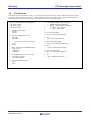
Contents
1.
Overview ............................................................................................................................................. 3
1.1 PTP Timer Synchronous Start Using FIT Modules ...................................................................... 3
1.2 Related documents ...................................................................................................................... 3
1.3 Terms and Abbreviations ............................................................................................................. 3
1.4 Hardware Structure ...................................................................................................................... 4
1.5 Software Structure ....................................................................................................................... 5
1.6 File Structure ................................................................................................................................ 7
2.
Functional Information ........................................................................................................................ 8
2.1 Hardware Requirements .............................................................................................................. 8
2.2 Hardware Resource Requirements ............................................................................................. 8
2.3 Software Requirements ............................................................................................................... 9
2.4 Supported Toolchains .................................................................................................................. 9
2.5 Header Files ................................................................................................................................. 9
2.6 Integer Types ............................................................................................................................... 9
2.7 Configuration Overview ................................................................................................................ 9
2.8 API Data Structures ................................................................................................................... 11
2.9 Return Values ............................................................................................................................ 11
2.10 Adding SDHI Driver to Your Project ........................................................................................... 12
2.11 Using without SDHI Driver ......................................................................................................... 12
3.
Specification of This Example .......................................................................................................... 13
3.1 Outline of Functions ................................................................................................................... 13
3.2 Environment and execution ....................................................................................................... 14
3.3 Board Setting ............................................................................................................................. 17
3.4 Demo Board Setting ................................................................................................................... 18
3.5 Measurement Examples ............................................................................................................ 19
4.
Provided Modules ............................................................................................................................. 21
5.
Reference Documents ...................................................................................................................... 21
R01AN1984EJ0102 Rev. 1.02
December 31, 2014
Page 2 of 21
RX Family
PTP Timer Synchronous Start
1. Overview
This document explains one of the typical usage examples of the PTP driver based on the firmware integration
technology (FIT). This example starts the Multi-Function Timer Pulse Unit (MTU3) or the General PWM Timer (GPT)
at a specific synchronous time via Event Link Controller (ELC) without CPU operation. The time synchronization
protocol is applied to the PTP. Users can observe the phase differences of the output PWM waves and can use the
software sample to implement their own system such as the motor control one.
1.1
PTP Timer Synchronous Start Using FIT Modules
This module is implemented in a project and used as the application example of the PTP Driver FIT Module.
1.2
Related documents
[1] IEEE Standard for a Precision Clock Synchronization Protocol for Networked Measurement and Control Systems,
Revision of IEEE Std 1588-2008, Mar 2008
[2] RX Family EPTPC Module Using Firmware Integration Technology, Rev.1.02, Document No. R01AN1943EJ0102,
Dec 31, 2014
[3] RX Family PTP Get Synchronous Time Using Firmware Integration Technology Modules, Rev.1.02, Document No.
R01AN1983EJ0102, Dec 31, 2014
[4] RX Family Ethernet Module Using Firmware Integration Technology, Rev.1.01, Document No. R01AN2009EJ0101,
Dec 16, 2014
[5] RX Family TCP/IP for Embedded system M3S-T4-Tiny: Introduction Guide Firmware Integration Technology,
Rev.2.00, Document No. R20AN0051EJ0200, Apr 01, 2014
[6] RX Family SDHI Driver Firmware Integration Technology Module, Rev.1.00, Document
No.RTM0RX0000DSDD0SD0RP
[7] Renesas USB MCU USB Basic Host and Peripheral firmware Using Firmware Integration Technology, Rev.1.00,
Document No. R01AN0025EJ0100, 2014
[8] Renesas USB MCU USB Host Mass Storage Class Driver (HMSC) Using Firmware Integration Technology,
Rev.1.00, Document No. R01AN0026EJ0100, 2014
[9] RX Family Open Source FAT File System [M3S-TFAT-Tiny] Module Firmware Integration Technology, Rev.3.00,
Document No. R20AN0038EJ0300, Apr 01, 2014
[10] Renesas Starter Kit+ for RX64M, User’s Manual, to be published
[11] HMI expansion demo board R0K50564MB000BR, User’s Manual, to be published
1.3
Terms and Abbreviations
IEEE1588
Specification makes the time synchronization in a communication network. In general, the communication network is
specified the Ethernet. There are two versions which are IEEE1588-2002 (version1) and IEEE1588-2008 (version2),
they do not have complete compatibilities each other. This document only attributes the IEEE1588-2008 (version2).
PTP (Precision Time Protocol)
PTP means time synchronize protocol based on the IEEE1588.
PTP message
The data format which is used in the PTP sequence. PTP messages are transmitted in the Ethernet frame (Layer2) or
UDP packet (Layer3).
R01AN1984EJ0102 Rev. 1.02
December 31, 2014
Page 3 of 21
RX Family
PTP Timer Synchronous Start
Clock (Node)
Device whose functionality is time synchronization based on the IEEE1588.
Local clock
Synchronize time of the each clock.
Master
Master means the Clock issues the system standard time to other clocks.
Slave
Slave means the Clock receives and corrects the system standard time to other clocks.
OC (Ordinary Clock)
OC means the Clock has only one port and one local clock.
BC (Boundary Clock)
BC means the Clock has more than two ports and common unique local clock. Each port has time synchronize function.
TC (Transparent Clock)
TC means the Clock has more than two ports and corrects the frame propagation delay between ingress and egress ports.
E2E (End to End)
Synchronize mode in which between a master and multiple Slaves (or a Slave).
P2P (Peer to Peer)
Synchronize mode in which between the specific two clocks.
STCA (Statistical Time Correction Algorithm)
Correct offsetFromMaster1 applied to statistical method to which estimates the tendencies of clock (time) deviation
from the gradient calculated using sampled clock values with (worst-10 filter).
BMC (Best Master Clock) algorithm
BMC algorithm determines the suitable master in the domain and composes of the data set comparison algorithm and
the state decision one. Data set comparison algorithm decides which port2 is better as master comparing the feature of
each clock. State decision algorithm decides the next state of the port as the result of the data set comparison algorithm.
1
Time difference between time on the Master and time on the Slave (refer to [1]).
2
One port of the clock. If clock has only one port, port equals to clock.
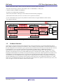
1.4
Hardware Structure
The Ethernet peripheral modules of the RX64M/71M group are composed of the EPTPC, the PTP Host interface
peripheral module (PTPEDMAC), dual channel Ethernet MAC ones (ETHERC (CH0), ETHERC (CH1)) and dual
channel Ethernet Host interface ones (EDMAC (CH0), EDMAC (CH1)). The EPTPC is divided to PTP Frame
Operation (CH0) part, PTP Frame Operation (CH1) part, Packet Relation Control part and Statistical Time Correction
Algorithm part from their functionality. EPTPC is also connected to the motor control timers (MTU3 and GPT
peripheral modules) via ELC peripheral module to synchronous activation of multiple motors.
Followings are the summary of the Ethernet peripheral modules and Figure 1.1 shows the related hardware’s block
diagram.
1. Synchronous function (EPTPC and PTPEDMAC)
- Based on the IEEE1588-2008 Version2
- Time synchronous function issuing PTP messages (Ethernet frame1 and UDP IPv4 format2)
- Master and Slave, OC, BC, TC functionality
- Time deviation is corrected by the statistical correction method (Gradient prediction time correction algorithm)
- Timer event output (6CH, rise/fall edges, event flag auto clear)
R01AN1984EJ0102 Rev. 1.02
December 31, 2014
Page 4 of 21
RX Family
PTP Timer Synchronous Start
- Motor control timer (MTU3, GPT) is started synchronously with the timer event via ELC
- Selectable PTP message operation (PTP module, CPU via PTPEDMAC, to other port)
2. Ethernet module (ETHERC and EDMAC)
- Possible to use independent 2CH Ethernet
- HW switch (selectable Cut Through or Store & Forward internal frame propagation)
- HW multicast frame filter (all receive, all cancel, receive specific two frames)
1
In case of RX64M Group, supports only Ethernet II frame format (not support IEEE802.3 frame format)
2
Not supports UDP IPv6
Synchronous parts
Host IF
EDMAC (CH0)
EPTPC
PTPEDMAC
EDMAC (CH1)
Packet Relation Control
PTP Frame
Operation (CH0)
ETHERC (CH0)
MII/RMII
PTP Frame
Operation (CH1)
Interrupt
Statistical Time
Correction
Algorithm
Local
Time Counter
Timer
Event
Outputs
(6CH)
MTU3
ELC
GPT
ETHERC (CH1)
MII/RMII
Figure 1.1 Hardware block diagram
1.5
Software Structure
This sample is operations example of the application layer. Those operations are to get a PTP configuration such as
MAC address, IP address, the kind of Clock, Master or Slave and delay mechanism (P2P or E2E) from the SD card, set
the PTP configuration to the PTP driver, get a specific timer start time from the SD card, set the specific timer start time
to the PTP driver, set an event link connection between EPTPC and MTU3/GPT, set PMM output setting to
MTU3/GPT driver and control the PTP protocol sequences using the PTP and Ether driver. The PTP driver always
should be used with Ether drivers [4]. TCP/IP middle ware does not include in this example. Therefore, user needs to
implement TCP/IP middle ware (ex.M3S-T4-Tiny the RX Family [5]) when this example applied to the TCP/IP system.
The SDHI driver [6] does the SD card access operations such as card mount, data read, write, erase, card detection,
write protection, etc. The USB Host driver [7], [8], which is implemented ATA interface and USB mass storage class,
does the USB memory access operations such as memory mount, data read, write, USB memory detection, etc. M3STFS-Tiny [9] is implemented as the FAT file system and it does the file access operations such as file open, close, read,
write, etc. Figure 1.2 shows the software structure of this sample.
R01AN1984EJ0102 Rev. 1.02
December 31, 2014
Page 5 of 21
RX Family
PTP Timer Synchronous Start
Timer sync start sample
Raw PTP
TCP/IP system
Motor control system
Storage system
This Sample (PTP Timer Synchronous Start Using FIT Modules)
Get/set PTP configuration (MAC address, IP address, Clock, Master/slave, P2P/E2E), Get/set specific timer start time, Set
ELC,Set MTU3, Set GPT, PTP protocol sequence ctrl
TCP/IP (Not use)
Middle Packet (TCP/IP, UDP/IP) trans/receive
ware Connection manage
PTP UDP/IP (Not use)
Ether Driver(CH0) and Ether Driver(CH1) ctrl
Driver
FAT (M3S-TFS-Tiny)
PTP UDP/IP
trans/receive
PTP Driver ctrl
Open/close file
File read
File write
Ether Driver(CH0)
Ether Driver(CH1)
PTP Driver
ELC Driver
MTU3 Driver
Frame trans/receive
Node manage
EDMAC(CH0) ctrl
ETHERC(CH0) ctrl
Cable detect
Frame trans/receive
Node manage
EDMAC(CH1) ctrl
ETHERC(CH1) ctrl
Cable detect
PTP frame
Node manage
Time sync
Event setting
BMC operation
PTPEDMAC ctrl
EPTPC ctrl
Event link set
Connect
EPTPC event
to MTU3
/GPT start
PWM
output
MTU3 ctrl
EDMAC(CH0)
EDMAC(CH1)
PTPEDMAC
ELC
MTU3
GPT Driver
PWM
output
GPT ctrl
GPT
SDHI Driver or
USB Host Driver
Card or USB
memory mount
Data read
Data write
Card or USB
memory detection
SDHI or USB
SD Socket or
USB connector
EPTPC
ETHERC(CH1)
ETHERC(CH0)
MII/RMII
MII/RMII
SD card
USB
memory
Figure 1.2 Software structure of this sample
R01AN1984EJ0102 Rev. 1.02
December 31, 2014
Page 6 of 21
RX Family
1.6
PTP Timer Synchronous Start
File Structure
This sample codes are stored the “demo_src” and low hierarchical folders. ELC, MTU3 and GPT drivers are stored
each driver folders respectively. Figure 1.3 shows the file structure of this sample. As for other FIT based modules
include the PTP driver FIT module, refer to the documentation of the each FIT module.
demo_src: main operation and configuration
| ptp_demo_config.h
| ptp_demo_main.c
| ptp_demo_main.h
|
+ --- file: File access control
|
apl_file.c
|
apl_file.h
|
+ --- led_7seg: 7segment led control
|
led_7seg.c
|
led_7seg.h
|
+ --- sync: PTP synchronize operation
|
sync.c
|
sync.h
|
+ --- tfat_if: File system IF to SDHI/USB driver
|
r_tfat_drv_if.c
|
r_data_file.c
|
r_data_file.h
|
+ --- usb: USB Host memory access control
|
usb_memory_access.c
|
r_usb_hmsc_defep.c
|
+ --- usr: LED and switch control
|
led.c
|
led.h
|
+ --- card_sample: Sample of SD card format
|
+ --- PARAM: Parameter sample files
|
+ --- PULSE: Timer start time sample files
|
+ --- MTU3: Case of MTU3
|
+ --- GPT: Case of GPT
|
r_elc_rx: ELC driver folder
| r_elc_rx_if.h ;ELC driver header file
|
+ --- src:
|
r_elc.c ; ELC driver source file
r_mtu3_rx: MTU3 driver folder
| r_mtu3_rx_if.h ;MTU3 driver header file
|
+ --- src:
|
r_mtu3.c ; MTU3 driver source file
r_gpt_rx: GPT driver folder
| r_gpt_rx_if.h ;GPT driver header file
|
+ --- src:
|
r_gpt.c ; GPT driver source file
Figure 1.3 File structure of this example
R01AN1984EJ0102 Rev. 1.02
December 31, 2014
Page 7 of 21
RX Family
PTP Timer Synchronous Start
2. Functional Information
This example is developed by the following principles.
2.1
Hardware Requirements
This driver requires your MCU supports the following feature:
EPTPC
PTPEDMAC
ETHERC
EDMAC
ELC
MTU3
GPT
CMT
SDHI (optional)
USB (optional)
2.2
Hardware Resource Requirements
This section details the hardware peripherals that this driver requires. Unless explicitly stated, these resources must be
reserved for the driver, and the user cannot use them.
2.2.1
ETHERC Channel
The example uses the ETHEC (CH0), ETHEC (CH1) or both depend on the kind of Clock (Node). Those resources
need to the Ethernet MAC operations.
2.2.2
EDMAC Channel
The example uses the EDMAC (CH0), EDMAC (CH1) or both depend on the kind of Clock (Node). Those resources
need to the CPU Host interface of standard Ethernet frame operations.
2.2.3
ELC
The example uses the ELC to connect events between EPTPC and MTU3/GPT. Those resources need to start the
MTU3/GPT synchronously.
2.2.4
MTU3 Channel
The example uses an MTU3 channel for the synchronous PWM output. Please do not modify the settings or try to use
the peripheral during driver operations.
2.2.5
GPT Channel
The example uses a GPT channel for the synchronous PWM output. Please do not modify the settings or try to use the
peripheral during driver operations.
2.2.6
SDHI Channel (optional)
The example uses a SDHI channel to load the configuration parameter and save the synchronized result. Please do not
modify the settings or try to use the peripheral during driver operations.
2.2.7
USB Channel (optional)
The example uses a USB channel to load the configuration parameter and save the synchronized result. Please do not
modify the settings or try to use the peripheral during driver operations.
R01AN1984EJ0102 Rev. 1.02
December 31, 2014
Page 8 of 21
RX Family
2.3
PTP Timer Synchronous Start
Software Requirements
This example is dependent upon the following packages:
r_bsp
r_ptp_rx
r_ether_rx
r_mtu3_rx
r_gpt_rx
r_sdhi_rx (Not packaged in this version. As for providing, refer to Sec 4.)
r_usb_basic
r_usb_hmsc
r_tfat
r_cmt_rx
2.4
Supported Toolchains
This example is tested and works with the following toolchain:
2.5
Renesas RX Toolchain v2.01.00
Header Files
Each functions call are accessed by including a single file, ptp_demo_config.h, ptp_demo_main.h, apl_file.h, sync.h,
r_data_file.h, r_elc_rx_if.h, r_mtu3_rx_if.h, r_gpt_rx_if.h or led_7seg.h which is supplied with this driver’s project
code.
2.6
Integer Types
This project uses ANSI C99. These types are defined in stdint.h.
2.7
Configuration Overview
The configuration options in this example are specified in ptp_demo_config.h, ptp_demo_main.h apl_file.h, sync.h and
r_data_file.h. The option names and setting values are listed in the table below.
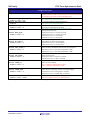
Configuration options
#define USE_MEDIA
#define MEDIA_NONE (0)
#define MEDIA_SD
(1)
#define MEDIA_USB (2)
- Default value = 1
#define USE_7SEG_LED
- defined
#define NUM_CHANNEL
- Default value = 1
#define DUAL_LINK
- defined
R01AN1984EJ0102 Rev. 1.02
December 31, 2014
Specify the kind of external storage media.
- When this is set to 0, no storage uses.
- When this is set to 1, use SD card.
- When this is set to 2, use USB memory.
Use 7segment LED1 or not.
- When “USE_7SEG_LED” is defined, use 7segment LED.
- When “USE_7SEG_LED” is not defined, not use 7segment
LED.
Specify the number of using Ethernet channels.
- Set 1 or 2 in the RX64M.
If clock is OC port1, BC or TC, you need set to 2.
Specify the Ethernet access channels.
- When “DUAL_LINK” is defined, 2 Ethernet channels access.
- When “DUAL_LINK” is not defined, Ethernet channels access
Page 9 of 21
RX Family
PTP Timer Synchronous Start
Configuration options
depend on the kind of clock.
If define “DUAL_LINK” and use one port only, you need link on
the remaining port (cable connected Ethernet hub).
#define TIMES_W10_INTERVAL
- Default value = 32
#define GET_SYNC_INFO
- defined
#define DEVICE_ID
- Default value = 0
#define MODE_PORT
- Default value = 0
#define MS_PORT0/1
- Default value = 0
#define SYNC_PORT0/1
- Default value = 1
This setting is not valid of this demo.
Get offsetFromMaster and meanPathDelay.
This setting is not valid of this demo.
This setting is only valid when no external media.
Set the device id number of the demo.
This setting is only valid when no external media.
Specify the kind of clock.
- When this is set to 0, clock is OC port0.
- When this is set to 1, clock is OC port1.
- When this is set to 2, clock is BC.
- When this is set to 3, clock is TC.
This setting is only valid when no external media.
Select Master or Slave for port0/port1
- When this is set to 0, clock is Master.
- When this is set to 1, clock is Slave.
This setting is only valid when no external media.
Select the delay mechanism (P2P or E2E) for port0/port1
- When this is set to 0, the delay mechanism is P2P.
- When this is set to 1, the delay mechanism is E2E.
#define USE_TIMER
- Default value = 0
This setting is only valid when no external media.
Select the using timer
- When this is set to 0, MTU3 is selected.
- When this is set to 1, GPT is selected.
#define TIMER_CH
- Default value = 0
This setting is only valid when no external media.
Select the timer channel.
- Set 0 (channel 0) when MTU3 is used.
- Set 1 (channel 1) when GPT is used.
#define TIMER_EDGE
- Default value = 0
This setting is only valid when no external media.
Select the rise or fall edge of ELC event signal trigger.
- When this is set to 0, rising edge is selected.
- When this is set to 1, falling edge is selected.
#define FILESIZE
- Default value = 2048
Specify the FAT file system data buffer size
- Set 2048 (default value) in the RX64M/71M.
1
This is implemented on the optional demo board (refer to [11]).
R01AN1984EJ0102 Rev. 1.02
December 31, 2014
Page 10 of 21
RX Family
2.8
PTP Timer Synchronous Start
API Data Structures
This section details the data structures that are used with the functions of this example. Those structures are located in
apl_file.h as the prototype declarations.
/* Get synchronous time demo configuration structure */
typedef struct {
uint8_t id;
uint8_t mac[2][6];
uint8_t ip[2][4];
uint8_t mode;
uint8_t ms[2];
uint8_t sync[2];
uint8_t prior;
uint8_t cls;
} SyncConfig;
/* Timer synchronous start demo configuration structure */
typedef struct {
uint8_t tmr;
uint8_t ch;
uint8_t edge;
uint32_t time_u;
uint32_t time_l;
} PulseConfig;
2.9
Return Values
This section describes return values of the functions of this example. Those return values are located in apl_file.h,
r_elc_rx_if.h, r_mtu3_rx_if.h, r_gpt_rx_if.h and led_7seg.h as the prototype declarations.
/* File access return value */
FILE_OK (0) /* No error */
FILE_ERROR (-1) /* General error */
/* ELC driver return value */
ELC_OK (0) /* No error */
ELC_ERROR (-1) /* General error */
/* MTU3 driver return value */
MTU3_OK (0) /* No error */
MTU3_ERROR (-1) /* General error */
/* GPT driver return value */
GPT_OK (0) /* No error */
GPT_ERROR (-1) /* General error */
/* 7segment LED driver return value */
LED_7SEG_OK (0) /* No error */
LED_7SEG_ERR (-1) /* General error */
R01AN1984EJ0102 Rev. 1.02
December 31, 2014
Page 11 of 21
RX Family
2.10
PTP Timer Synchronous Start
Adding SDHI Driver to Your Project
The SDHI driver is not packaged in this sample project. When you use the SDHI driver, you need to get the SDHI
driver and add it to this sample project following. As for providing, refer to Sec.4.
Adding the SDHI driver (when not using the plug-in)
1.
Please put the SDHI driver in the root folder (“RX64M/71M_PTP_SyncStart”).
2.
Select the SD card in the “USE_MEDIA” option (refer to 2.7)
3.
Rebuild the project.
2.11
Using without SDHI Driver
The SDHI driver is not packaged in this sample project. If you use this sample without SDHI driver, you need to do
following procedure before using this sample.
Procedure using without SDHI Driver
1. Please release the SDHI driver from the build tree in the project. The SDHI driver’s build trees are “r_sdhi_rx” and
bellows.
2.
Select the MEDIA_USB or MEDIA_NONE in the “USE_MEDIA” option (refer to 2.7).
3.
Rebuild the project.
Remarks of USB used case setting
1.
This example does not support USB hub. Please connect a USB memory to the connector directory.
2.
USB memory should be attached to connector before starting this example.
Remarks of no media used case setting
Assume you use board1 and board2, and those modes are OC and using port is only port0.
1.
Need to port1 link on (cable connected Ethernet hub) or not define “DUAL_LINK” option (refer to 2.7).
2.
Change configuration
Change the demo_src/file/apl_file.h setting.
board1: DEVICE_ID (0), MS_PORT0 (0) /* Master */ – default setting
board2: DEVICE_ID (1), MS_PORT0 (1) /* Slave */ – remaining are default setting
3.
Start running SW
When the timer stat time is coincident the local clock time, you can will observe the PWM waves.
R01AN1984EJ0102 Rev. 1.02
December 31, 2014
Page 12 of 21
RX Family
PTP Timer Synchronous Start
3. Specification of This Example
3.1
Outline of Functions
The function of this example shows Table 3.1.
Table 3.1 Function of This Example
Item
main()
create_eval_dir()
delete_eval_dir()
save_sync_result()
get_sync_config()
get_pulse_time()
ReadPTPMsg()
GetLcClk()
EINT_Trig_isr()
Write_to_Media()
IsTrigPacket()
R_tfat_disk_initialize()
R_tfat_disk_read()
R_tfat_disk_write()
R_tfat_disk_ioctl()
R_tfat_disk_status()
R_tfat_get_fattime()
R_card_insertion_chk()
R_ELC_Init()
R_ELC_Set_Timer_Event()
R_ELC_Ctr_Timer_Event()
R_MTU3_Init()
R_MTU3_Start()
R_MTU3_Stop()
R_GPT_Init()
R_GPT_Start()
R_GPT_Stop()
R_LED_Open ()
R_LED_UpdTime()
rx64m_led_cmt_cyclic_isr()
R_CMT_CreatePeriodic()
R01AN1984EJ0102 Rev. 1.02
December 31, 2014
Contents
Main operation of the typical usage example of the PTP driver.
Create evaluation directories.
Delete evaluation directories.
Save synchronous time to the media. Not used of this demo.
Get synchronous test configuration.
Get pulse activate time.
Read PTP messages. If announce message is received, update Master
port identity.
Get and save local clock counter. Not used of this demo.
Trigger packet received interrupt handler. Not used of this demo.
Write saved local clock counter to the media. Not used of this demo.
Check received frame is trigger packet or not. Not used of this demo.
Mount and initialize the media to file access.
Read data located on the specified address from the media.
Write data located on the specified address to the media.
Media control operations. (no operation in the RX64M/71M)
Get current status of the media. (no operation in the RX64M/71M)
Get current time. (not valid operation in the RX64M/71M).
Check any media inserted or not.
Initialize ELC (start ELC).
Connect EPTPC timer event to MTU3/GPT start event..
Enable/disable PTP timer event.
Initialize MTU3 (PWM mode1 setting).
Start MTU3 counter. Not used of this demo.
Stop MTU3 counter. Not used of this demo.
Initialize GPT (saw PWM mode setting).
Start GPT counter. Not used of this demo.
Stop GPT counter. Not used of this demo.
Initialize and open 7segment LED.
Update data to show 7segment LED.
7segment LED interrupt handler. (output data on the 7segment LED)
Set periodic interrupt from CMT.
Page 13 of 21
RX Family
3.2
PTP Timer Synchronous Start
Environment and execution
This example needs the Renesas Starter Kit+ for RX64M (hereafter RX64M RSK board) [10] or the Renesas Starter
Kit+ for RX71M (hereafter RX71M RSK board) more than two (Master node and Slave node), Ethernet Hub (hereafter
HUB) and the Oscilloscope. The PWM output pin of the each RX64M/71M RSK boards connects the input of the
oscilloscope. The outline of the execution sequence when SD cards are used is following. If USB memories are used,
this outline is same except for the media difference.
Each clock (RX64M/71M RSK board) gets the test configuration include a specific timer start time from the SD
card1 and start the synchronization one another.
Contents of SD card are composed of the parameter saved file (=PARAM.txt) and the timer start time saved files
(= TEST_1.txt). The fields of saved timer start time are higher and lower 32 bits of nanosecond order field
(=TMSTTRUm and TMSTTRLm).
If the optional demo board is equipped[11], the 7segment LED also shows the timer start time. The field of showed
the timer start time is lower 32 bits of nanosecond order field (=TMSTTRLm).
Each clock starts the MTU3/GPT timer via ELC when their local clock counter synchronized of the PTP compares
match the specific time.
User can observe the phase differences of the output PWM waves.
1
Need to select the SD card in the “USE_MEDIA” option (refer to 2.7).
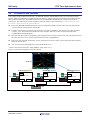
Figure 3.1 shows the configuration using three boards.
Oscilloscope
RX64M RSK board 1
RX64M RSK board 2
SDHI
SDHI
ID = 0
Demo board
Port0
2
3
4
ID = 2
Demo board
Port1
1
SDHI
ID = 1
Demo board
Port0
RX64M RSK board 3
Port1
Port0
Port1
5
Hub
Figure 3.1 Environment (three boards configuration)
R01AN1984EJ0102 Rev. 1.02
December 31, 2014
Page 14 of 21
RX Family
PTP Timer Synchronous Start
Figure 3.2 and Figure 3.3 show the software flow overview and the format example of SD cards respectively. As for
samples of SD card format are equipped with “demo_src/card_sample folder”. Figure 3.4 and Figure 3.5 also show the
examples of the parameter saved file in the 3boards, OC and port0 configuration and the timer start time saved file
respectively.
Start
Initialize RX64M
(Modifies pins, set interrupt, etc)
Read parameter from SD card
Refer to PARAM.txt
Read timer start time from the SD card
Refer to PULSE/TEST_1.txt
Initialize EDMAC, ETHERC
Frame send/receive enable
Set EPTPC depends on the parameter
Start synchronous
HW operation
Time
coincidence?
No
Yes
via ELC
Start timer
Start PWM wave output
Observed by oscilloscope
End
Figure 3.2 Software flow overview
R01AN1984EJ0102 Rev. 1.02
December 31, 2014
Page 15 of 21
RX Family
PTP Timer Synchronous Start
SD card (need the number of boards)
Board 1
Board 2
Board N
PARAM.txt
(save parameter)
SD card contents
[ID] = 1 (or 2, ,,,)
[MAC0] = 021234567800
[MAC1] = 021234567810
[IP0] = 192.168.0.10
[IP1] = 192.168.0.20
[MODE] = OC0 (or OC1, BC, TC)
[MS] = Master (or Slave)
[SYNC0] = E2E (or P2P)
[SYNC1] = E2E (or P2P)
PULSE folder (save timer start time)
PARAM.txt
(save parameter)
[TMR] = MTU (or GPT)
[CH] = 0 (or 1, 2, 3, 4, 5)
[EDGE] = RISE (or FALL)
[ST_1_U] = 23456701
[ST_1_L] = ABCDEF89
TEST_1.txt
TEST_1.txt
Figure 3.3 Format example of SD cards
[ID] = 0
[MAC0] = 000102030405
[MAC1] = 101112131415
[IP0] = 06070809
[IP1] = 16171819
[MODE] = OC0
[MS0] = MASTER
[MS1] = MASTER
[SYNC0] = E2E
[SYNC1] = E2E
[ID] = 1
[MAC0] = 202122232425
[MAC1] = 303132333435
[IP0] = 26272829
[IP1] = 36373839
[MODE] = OC0
[MS0] = SLAVE
[MS1] = SLAVE
[SYNC0] = E2E
[SYNC1] = E2E
[ID] = 2
[MAC0] = 404142434445
[MAC1] = 505152535455
[IP0] = 46474849
[IP1] = 56575859
[MODE] = OC0
[MS0] = SLAVE
[MS1] = SLAVE
[SYNC0] = E2E
[SYNC1] = E2E
PARAM.txt
(ID = 0, OC, Port0)
PARAM.txt
(ID = 1, OC, Port0)
PARAM.txt
(ID = 2, OC, Port0)
Figure 3.4 Example of the parameter saved files
[TMR] = MTU
[CH] = 3
[EDGE] = RISE
[ST_1_U] = 13B5834F
[ST_1_L] = 1A43C200
TEST_1.txt
(MTU3, CH = 3, RISE Edge)
[TMR] = GPT
[CH] = 4
[EDGE] = FALL
[ST_1_U] = 13B58350
[ST_1_L] = BB7F4400
TEST_1.txt
(GPT, CH = 4, FALL Edge)
Figure 3.5 Example of the timer start time saved files
R01AN1984EJ0102 Rev. 1.02
December 31, 2014
Page 16 of 21
RX Family
3.3
PTP Timer Synchronous Start
Board Setting
There are several jumpers and switches changing from the default setting of the RX64M/71M RSK board1 to execute
this example. Figure 3.6 and Figure 3.7 indicate their changing and related functions SD card used case and USB
memory used case respectively.
1
Product number: R0K50564MC001BR/R0K5RX71MC010BR.
Jumper/Switch
J3
J4
J15
SW8-1
SW8-2
SW8-3
SW8-4
SW8-5
SW8-6
SW8-7
SW8-8
SW8-9
SW8-10
SW9-1
SW9-2
SW9-3
SW9-4
SW9-7
SW9-8
Default setting
2-3
2-3
1-2
ON
OFF
ON
OFF
ON
OFF
ON
OFF
ON
OFF
ON
OFF
ON
OFF
ON
OFF
Demo setting
1-2
1-2
2-3
OFF
ON
OFF
ON
OFF
ON
OFF
ON
OFF
ON
OFF
ON
OFF
ON
OFF
ON
Functional use
ETHERC ET0MDIO (CH0)
ETHERC ET0MDC (CH0)
MTU3 MTIOC0C
SDHI SDD2-B
SDHI SDD3-B
SDHI SDCMD-B
SDHI SDCLK-B
SDHI SDD0-B
SDHI SDD1-B
SDHI SDCD-B
SDHI SDWP-B
Figure 3.6 Jumper/Switch setting (SD card used case)
Jumper/Switch
J2
J3
J4
J6
J15
Default setting
2-3
2-3
2-3
1-2
1-2
Demo setting
1-2
1-2
1-2
2-3
2-3
Functional use
USB Enables Host Mode
ETHERC ET0MDIO (CH0)
ETHERC ET0MDC (CH0)
USB USB0VBUSEN
MTU3 MTIOC0C (CH0)
Figure 3.7 Jumper/Switch setting (USB memory used case)
User need to connect the PWM output pin of the RX64M/71M RSK board to the oscilloscope pin. Figure 3.8 indicates
the board pins outputted PWM wave.
Application header
JA2
JA3
Pin
23
18
Header name
IRQ2/M1_EncZ/M1_HSIN2
D1
MCU pin
29
156
PWM output timer
MTU3 MTIOC0C (CH0)
GPT GTIOC1A (CH1)
Figure 3.8 PWM output pins
R01AN1984EJ0102 Rev. 1.02
December 31, 2014
Page 17 of 21
RX Family
3.4
PTP Timer Synchronous Start
Demo Board Setting
There are several resistances changing from the default setting of the demo board to use the 7segment LED. Figure 3.9
indicates their changing from default setting.
Resistance
R387
R433
R464
R348
R404
R429
R445
Default setting
Mount
Mount
Mount
Remove
Remove
Remove
Remove
Demo setting
Remove
Remove
Remove
Mount
Mount
Mount
Mount
Functional use
7segment LED
7segment LED
7segment LED
7segment LED
7segment LED
7segment LED
7segment LED
Figure 3.9 Resistance setting (7segment LED used case)
R01AN1984EJ0102 Rev. 1.02
December 31, 2014
Page 18 of 21
RX Family
3.5
PTP Timer Synchronous Start
Measurement Examples
The measurement results of the three board configuration show followings as the reference data.
Please keep your mind those result are depend on the measurement condition and environment.
3.5.1
Condition
Topology
Using three RX64M/71M RSK boards, OC E2E.
Synchronous mode
The gradient correction, which is the functionality of STCA unit, was applied (=mode2).
PWM output timer
Using MTU3 channel3 and GPT channel4.
PTP commands interval
PTP commands interval was 1sec1.
1
The intervals of Sync and Delay_Req message were 1sec.
3.5.2
Method
We measured the PWM output waves using oscilloscope (Identical configuration of the Figure 3.1) when MTU3 and
GPT applied to PWM output timer.
R01AN1984EJ0102 Rev. 1.02
December 31, 2014
Page 19 of 21
RX Family
3.5.3
PTP Timer Synchronous Start
Result
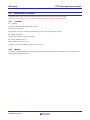
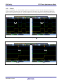
Figure 3.10 and Figure 3.11 show the PWM output waves using MTU3 channel3 and GPT channel4 and those time
scale are 100sec and 100nsec per unit coordinate respectively. The yellow line, green line and blue line indicate the
Master, Slave1 and Slave2 respectively. The phase differences of the output PWM waves were approximately 100nsec.
Yellow line(CH1): Master
Green line(CH2): Slave1
Blue line(CH3): Slave2
100sec
100sec
MTU3
GPT
Figure 3.10 PWM wave example (100sec scale unit)
Yellow line(CH1): Master
100nsec
MTU3
Green line(CH2): Slave1
Blue line(CH3): Slave2
100nsec
GPT
Figure 3.11 PWM wave example (100nsec scale unit)
R01AN1984EJ0102 Rev. 1.02
December 31, 2014
Page 20 of 21
RX Family
PTP Timer Synchronous Start
4. Provided Modules
The module provided can be downloaded from the Renesas Electronics website.
SD driver (r_sdhi_rx) can be provided the customer who licenses HALA1 (Host/Ancillary Product License Agreement)
and SDHI NDA.
To get SDHI driver, please contact following the Inquiries.
Inquiries: http://www.renesas.com/contact/
1
HALA License: Licenses for manufacturing/selling SD host related products.
5. Reference Documents
User’s Manual: Hardware
RX64M Group User’s Manual: Hardware Rev.1.00 (R01UH0377EJ)
The latest version can be downloaded from the Renesas Electronics website.
User’s Manual: Software
RX Family RXv2 Instruction Set Architecture User’s Manual: Hardware Rev.1.00 (R01US0071EJ)
The latest version can be downloaded from the Renesas Electronics website.
Technical Update/Technical News
The latest information can be downloaded from the Renesas Electronics website.
Website and Support
Renesas Electronics website
http://www.renesas.com
Inquiries
http://www.renesas.com/contact/
R01AN1984EJ0102 Rev. 1.02
December 31, 2014
Page 21 of 21
REVISION HISTORY
Rev.
Date
1.00
1.01
1.02
-
Jul 10, 2014
Aug 20, 2014
Dec 31, 2014
-
RX Family Application Note
PTP Timer Synchronous Start Using Firmware Integration
Technology Modules
Page
—
—
—
—
Description
Summary
First edition issued.
Optional 7segment LED function added.
Applied PTP driver Rev.1.02 and changed file structure.
All trademarks and registered trademarks are the property of their respective owners.
A-1
General Precautions in the Handling of MPU/MCU Products
The following usage notes are applicable to all MPU/MCU products from Renesas. For detailed usage notes on the
products covered by this document, refer to the relevant sections of the document as well as any technical updates that
have been issued for the products.
1. Handling of Unused Pins
Handle unused pins in accordance with the directions given under Handling of Unused Pins in the
manual.
The input pins of CMOS products are generally in the high-impedance state. In operation with an
unused pin in the open-circuit state, extra electromagnetic noise is induced in the vicinity of LSI, an
associated shoot-through current flows internally, and malfunctions occur due to the false
recognition of the pin state as an input signal become possible. Unused pins should be handled as
described under Handling of Unused Pins in the manual.
2. Processing at Power-on
The state of the product is undefined at the moment when power is supplied.
The states of internal circuits in the LSI are indeterminate and the states of register settings and
pins are undefined at the moment when power is supplied.
In a finished product where the reset signal is applied to the external reset pin, the states of pins
are not guaranteed from the moment when power is supplied until the reset process is completed.
In a similar way, the states of pins in a product that is reset by an on-chip power-on reset function
are not guaranteed from the moment when power is supplied until the power reaches the level at
which resetting has been specified.
3. Prohibition of Access to Reserved Addresses
Access to reserved addresses is prohibited.
The reserved addresses are provided for the possible future expansion of functions. Do not access
these addresses; the correct operation of LSI is not guaranteed if they are accessed.
4. Clock Signals
After applying a reset, only release the reset line after the operating clock signal has become stable.
When switching the clock signal during program execution, wait until the target clock signal has
stabilized.
When the clock signal is generated with an external resonator (or from an external oscillator)
during a reset, ensure that the reset line is only released after full stabilization of the clock signal.
Moreover, when switching to a clock signal produced with an external resonator (or by an external
oscillator) while program execution is in progress, wait until the target clock signal is stable.
5. Differences between Products
Before changing from one product to another, i.e. to a product with a different part number, confirm
that the change will not lead to problems.
The characteristics of an MPU or MCU in the same group but having a different part number may
differ in terms of the internal memory capacity, layout pattern, and other factors, which can affect
the ranges of electrical characteristics, such as characteristic values, operating margins, immunity
to noise, and amount of radiated noise. When changing to a product with a different part number,
implement a system-evaluation test for the given product.
Notice
1.
Descriptions of circuits, software and other related information in this document are provided only to illustrate the operation of semiconductor products and application examples. You are fully responsible for
the incorporation of these circuits, software, and information in the design of your equipment. Renesas Electronics assumes no responsibility for any losses incurred by you or third parties arising from the
use of these circuits, software, or information.
2.
Renesas Electronics has used reasonable care in preparing the information included in this document, but Renesas Electronics does not warrant that such information is error free. Renesas Electronics
assumes no liability whatsoever for any damages incurred by you resulting from errors in or omissions from the information included herein.
3.
Renesas Electronics does not assume any liability for infringement of patents, copyrights, or other intellectual property rights of third parties by or arising from the use of Renesas Electronics products or
technical information described in this document. No license, express, implied or otherwise, is granted hereby under any patents, copyrights or other intellectual property rights of Renesas Electronics or
others.
4.
You should not alter, modify, copy, or otherwise misappropriate any Renesas Electronics product, whether in whole or in part. Renesas Electronics assumes no responsibility for any losses incurred by you or
third parties arising from such alteration, modification, copy or otherwise misappropriation of Renesas Electronics product.
5.
Renesas Electronics products are classified according to the following two quality grades: "Standard" and "High Quality". The recommended applications for each Renesas Electronics product depends on
the product's quality grade, as indicated below.
"Standard": Computers; office equipment; communications equipment; test and measurement equipment; audio and visual equipment; home electronic appliances; machine tools; personal electronic
equipment; and industrial robots etc.
"High Quality": Transportation equipment (automobiles, trains, ships, etc.); traffic control systems; anti-disaster systems; anti-crime systems; and safety equipment etc.
Renesas Electronics products are neither intended nor authorized for use in products or systems that may pose a direct threat to human life or bodily injury (artificial life support devices or systems, surgical
implantations etc.), or may cause serious property damages (nuclear reactor control systems, military equipment etc.). You must check the quality grade of each Renesas Electronics product before using it
in a particular application. You may not use any Renesas Electronics product for any application for which it is not intended. Renesas Electronics shall not be in any way liable for any damages or losses
incurred by you or third parties arising from the use of any Renesas Electronics product for which the product is not intended by Renesas Electronics.
6.
You should use the Renesas Electronics products described in this document within the range specified by Renesas Electronics, especially with respect to the maximum rating, operating supply voltage
range, movement power voltage range, heat radiation characteristics, installation and other product characteristics. Renesas Electronics shall have no liability for malfunctions or damages arising out of the
use of Renesas Electronics products beyond such specified ranges.
7.
Although Renesas Electronics endeavors to improve the quality and reliability of its products, semiconductor products have specific characteristics such as the occurrence of failure at a certain rate and
malfunctions under certain use conditions. Further, Renesas Electronics products are not subject to radiation resistance design. Please be sure to implement safety measures to guard them against the
possibility of physical injury, and injury or damage caused by fire in the event of the failure of a Renesas Electronics product, such as safety design for hardware and software including but not limited to
redundancy, fire control and malfunction prevention, appropriate treatment for aging degradation or any other appropriate measures. Because the evaluation of microcomputer software alone is very difficult,
please evaluate the safety of the final products or systems manufactured by you.
8.
Please contact a Renesas Electronics sales office for details as to environmental matters such as the environmental compatibility of each Renesas Electronics product. Please use Renesas Electronics
products in compliance with all applicable laws and regulations that regulate the inclusion or use of controlled substances, including without limitation, the EU RoHS Directive. Renesas Electronics assumes
no liability for damages or losses occurring as a result of your noncompliance with applicable laws and regulations.
9.
Renesas Electronics products and technology may not be used for or incorporated into any products or systems whose manufacture, use, or sale is prohibited under any applicable domestic or foreign laws or
regulations. You should not use Renesas Electronics products or technology described in this document for any purpose relating to military applications or use by the military, including but not limited to the
development of weapons of mass destruction. When exporting the Renesas Electronics products or technology described in this document, you should comply with the applicable export control laws and
regulations and follow the procedures required by such laws and regulations.
10. It is the responsibility of the buyer or distributor of Renesas Electronics products, who distributes, disposes of, or otherwise places the product with a third party, to notify such third party in advance of the
contents and conditions set forth in this document, Renesas Electronics assumes no responsibility for any losses incurred by you or third parties as a result of unauthorized use of Renesas Electronics
products.
11. This document may not be reproduced or duplicated in any form, in whole or in part, without prior written consent of Renesas Electronics.
12. Please contact a Renesas Electronics sales office if you have any questions regarding the information contained in this document or Renesas Electronics products, or if you have any other inquiries.
(Note 1)
"Renesas Electronics" as used in this document means Renesas Electronics Corporation and also includes its majority-owned subsidiaries.
(Note 2)
"Renesas Electronics product(s)" means any product developed or manufactured by or for Renesas Electronics.
SALES OFFICES
http://www.renesas.com
Refer to "http://www.renesas.com/" for the latest and detailed information.
Renesas Electronics America Inc.
2801 Scott Boulevard Santa Clara, CA 95050-2549, U.S.A.
Tel: +1-408-588-6000, Fax: +1-408-588-6130
Renesas Electronics Canada Limited
1101 Nicholson Road, Newmarket, Ontario L3Y 9C3, Canada
Tel: +1-905-898-5441, Fax: +1-905-898-3220
Renesas Electronics Europe Limited
Dukes Meadow, Millboard Road, Bourne End, Buckinghamshire, SL8 5FH, U.K
Tel: +44-1628-585-100, Fax: +44-1628-585-900
Renesas Electronics Europe GmbH
Arcadiastrasse 10, 40472 Düsseldorf, Germany
Tel: +49-211-6503-0, Fax: +49-211-6503-1327
Renesas Electronics (China) Co., Ltd.
Room 1709, Quantum Plaza, No.27 ZhiChunLu Haidian District, Beijing 100191, P.R.China
Tel: +86-10-8235-1155, Fax: +86-10-8235-7679
Renesas Electronics (Shanghai) Co., Ltd.
Unit 301, Tower A, Central Towers, 555 Langao Road, Putuo District, Shanghai, P. R. China 200333
Tel: +86-21-2226-0888, Fax: +86-21-2226-0999
Renesas Electronics Hong Kong Limited
Unit 1601-1613, 16/F., Tower 2, Grand Century Place, 193 Prince Edward Road West, Mongkok, Kowloon, Hong Kong
Tel: +852-2265-6688, Fax: +852 2886-9022/9044
Renesas Electronics Taiwan Co., Ltd.
13F, No. 363, Fu Shing North Road, Taipei 10543, Taiwan
Tel: +886-2-8175-9600, Fax: +886 2-8175-9670
Renesas Electronics Singapore Pte. Ltd.
80 Bendemeer Road, Unit #06-02 Hyflux Innovation Centre, Singapore 339949
Tel: +65-6213-0200, Fax: +65-6213-0300
Renesas Electronics Malaysia Sdn.Bhd.
Unit 906, Block B, Menara Amcorp, Amcorp Trade Centre, No. 18, Jln Persiaran Barat, 46050 Petaling Jaya, Selangor Darul Ehsan, Malaysia
Tel: +60-3-7955-9390, Fax: +60-3-7955-9510
Renesas Electronics Korea Co., Ltd.
12F., 234 Teheran-ro, Gangnam-Ku, Seoul, 135-920, Korea
Tel: +82-2-558-3737, Fax: +82-2-558-5141
© 2014 Renesas Electronics Corporation. All rights reserved.
Colophon 4.0