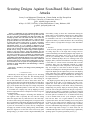
1
Securing Designs Against Scan-Based Side-Channel
Attacks
Jeremy Lee , Mohammad Tehranipoor , Chintan Patel , and Jim Plusquellic
ECE Dept.,
University of Connecticut, Storrs, CT
jslee, tehrani @engr.uconn.edu
Dept. of CSEE, University
of Maryland Baltimore County, Baltimore, MD
cpatel2, plusquel @umbc.edu
Abstract— Traditionally, the only standard method of testing
that has consistently provided high fault coverage has been scan
test due to the high controllability and high observability this
technique provides. The scan chains used in scan test not only
allow test engineers to control and observe a chip, but these
properties also allow the scan architecture to be used as a means
to breach chip security. In this paper, we propose a technique,
called Lock & Key, to neutralize the potential for scan-based
side-channel attacks. It is very difficult to implement an all
inclusive security strategy, but by knowing the attacker, a suitable
strategy can be devised. The Lock & Key technique provides a
flexible security strategy to modern designs without significant
changes to scan test practices. Using this technique, the scan
chains are divided into smaller subchains. With the inclusion of a
test security controller, access to subchains are randomized when
being accessed by an unauthorized user. Random access reduces
repeatability and predictability making reverse engineering more
difficult. Without proper authorization, an attacker would need
to unveil several layers of security before gaining proper access to
the scan chain in order to exploit it. The proposed Lock & Key
technique is design independent while maintaining a relatively
low area overhead.
Index Terms— Lock & key, scan design, security, hacking, sidechannel attacks.
I. I NTRODUCTION
Modern day VLSI designs are placing an ever increasing
number of transistors on a single die. The increasing design
size translates to a higher probability of a fault existing on
the die after fabrication. In order to detect these faults, test
engineers must find a fast and reliable method of testing these
large designs before the chips can be passed on to consumers
[1][2]. If the product does not ship soon enough, competition
may have a comparable product to offer first, but if testing
is not reliable, the company may end up shipping too many
defective chips. Both of these consequences causes a large loss
in potential profit.
Testing of modern designs is becoming more difficult for
test engineers. This is especially the case with SoC testing
where the engineer has very limited access to the entire chip.
In order to make testing more manageable, test engineers must
have a method that would allow them high controllability and
observability over the chip. Controllability allows the engineer
to place the circuit under test (CUT) into any configuration
and apply any stimuli necessary during testing. Observability
allows the engineer to see the state of the circuit at any point
during testing [3]. In order to achieve high controllability and
observability, testing is taken into consideration during the
design phase of development. Design-for-test (DFT) allows
the test engineer access to the chip that would otherwise
be unavailable. Scan test is one method of DFT that gives
engineers the ability to control and observe the CUT allowing
them to achieve very high fault coverage in a fast and reliable
manner.
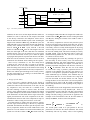
A. Scan Test
Scan has been generally accepted as the standard method
of testing chips due to the high fault coverage and low
overhead. Including scan while designing the chip requires one
additional pin to the primary I/O to serve as the test control
pin (TC) [3]. Internally, there is little impact on the design
since the standard flip-flops (FFs) are exchanged with scan
flip-flops (SFFs), which are then linked to one another creating
a scan chain. TC selects between functional and test mode
operations. SFFs carry the additional overhead of a single
two-to-one multiplexer when compared to the standard flipflop. An example of a scan chain is shown in Figure 1. TC
controls each multiplexer choosing between the normal mode
input of the flip-flop or the output of the previous scan flip-flop
in the chain. Due to the additional multiplexer, normal mode
performance could potentially be hindered since the output of
the combinational logic blocks are not directly connected to
the input of the FFs.
The flip-flop registers make up the I/O to the combinational
logic blocks in the chip, so test engineers are able to manipulate the values that are input (controllability) and view
the output (observability) of each block. This is performed by
multiplexing one primary input pin and one primary output
pin as the scan-in (SI) pin and scan-out (SO) pin, respectively.
Using the SI pin while TC is enabled, a test pattern is scanned
into the scan chain as dictated by the system clock [3]. When
the entire pattern is scanned in, TC is disabled and the chip
is run in normal mode for one cycle storing the responses
back into the SFFs. TC is again enabled to scan out the
response while at the same time scanning in a new test pattern
to check for new faults previous patterns were not able to
detect. Using this method of test, sequential logic essentially
becomes combinational logic during test. Creating test patterns
that achieve high fault coverage is a much easier task for
combinational logic than it is for sequential logic; significantly
speeding up the test pattern generation process [3].
PIs
POs
Combinational Logic
SI
SO
0
1
0
SFF1
1
0
SFF 2
1
0
SFF 3
1
0
SFF 4
1
0
SFF 5
1
0
SFF 6
1
0
SFF 7
1
SFF 8
TC
Clk
Fig. 1.
An example of a scan chain created from SFFs.
B. Chip Security
Security has become a greater concern in the design and
test of chips recently [4][5][6][7][8]. This has become more
apparent with the advent of cryptochips [9]. Cryptochips
perform encryption and decryption algorithms at the circuit
level. Many researchers have been able to show that these
chips are highly vulnerable to side-channel attacks using
power analysis [10], timing analysis [11], and fault-injection
[12][13]. These attacks are considered non-invasive and if not
considered carefully, strong encryption algorithms that would
take years to crack by brute force can otherwise be crippled
in a manner of weeks, days, or even hours without the need
to disassemble the chip packaging.
Recently, a new vulnerability has been shown to compromise on-chip data. Scan test has been proven a security risk to
the intellectual property (IP) on the chip and has become quite
a concern to the design and test communities [14][15][16][17].
Yang et al. [14] were able to simulate an attack on the scan
chain of a DES cryptochip to reveal the secret key with using
only three plaintexts. Although the scan chains have only been
exploited to find the secret key of a cryptochip, it is just
as easy to uncover proprietary intellectual property through
scan chains since vital registers are part of the chains that
are allowing high controllability and observability. Instead of
simply revealing fabrication defects, the scan chains are also
revealing protected IP.
Currently, the main objective in testing has been to control
and observe a chip as much as possible in order to achieve high
fault coverage and diagnosis on the CUT. As useful as these
properties are for testing, they are completely contradictory to
the objectives of security on a chip. In order to protect a chip
from malicious users, a chip must reveal as little as possible
while still considered useful to the end-user, but for reliability,
a test engineer needs as much access to the chip as possible.
C. Contribution and Paper Organization
In order to prevent IP theft, security measures must be
implemented during the design phase. However, similar to
design countermeasures of the more conventional side-channel
attacks, a design countermeasure from scan-based attacks
would prove futile against an invasive attack.
In this paper, we propose the Lock & Key security technique
in order to prevent aggressive users from maliciously attacking
the scan chains to reveal vital information about the chip using
non-invasive methods [18] and extend the work to include the
effect on DFT industrial flows and test applications techniques.
Our relatively low overhead security solution against scanbased side-channel attacks minimizes the controllability and
observability of the scan chain when an unauthorized user
attempts to access them. The Lock & Key technique divides
the scan chain into smaller subchains of equal length. The test
security controller used by this technique switches between
secure and insecure mode for authorized and unauthorized
users, respectively. When in secure mode, subchain operation
is predictable but non-sequential, but when insecure, subchain
operation is entirely random. This prevents malicious users
from predicting where in the scan chain the stimuli on SI
goes and where the response on SO comes from. The reduced
predictability and random access eliminates repeatability and
prevents reverse engineering.
This paper is organized as follows: In Section II, we will
discuss testability and security as it applies to modern designs
and how the two apply to modern day hackers. Section III
will discuss prior work performed in the field of chip test and
security. We will then propose and discuss our method of Lock
& Key security in Section IV. Section V presents an analysis
of our method. Finally, we will wrap up our discussion in
Section VI with the conclusion.
II. OVERVIEW: T ESTABILITY, S ECURITY
AND
H ACKING
Testability and security inherently contradict each other.
The testability of a chip can be defined by the amount of
controllability and observability the test engineer is granted.
The higher degree of controllability and observability allowed,
the easier it is to test the CUT. The test is not only easier to
perform, but the result of the test becomes more reliable due
to a higher fault coverage.
Security ensures that anything in a circuit is safely stored
within itself. The most common manner of providing security
is to hide the information behind some form of recognition that
would be able to tell a valid user from an attacker. Modern
day security in all realms use this method to protect vital
belongings, whether it is a security code for a home, retinal
scanner for a lab, or encryption key for information. Security
relies on making information obscure and difficult to figure
out.
When trying to relate testability and security together in
chip design, security is clearly contradicted by testability. By
designing for testability, a designer is essentially revealing all
information about the chip through the use of scan test. If the
aim of designing a chip is security, it is very difficult to justify
the amount of controllability and observability that testability
aims to provide because of these leaks. It is also necessary,
however, to ensure the chip will function properly through
testing in a fast and reliable manner. The only system secure
from any leaks is one without any controllable inputs nor
observable outputs, but this is absurd from both a testability
and usability standpoint.
Much of this concern over chip security would not be necessary unless the IP needed to be protected from malicious users
and hackers. There are many hackers in the world with many
different motivations. They range from the noble, attempting
to make their fellow developers aware of their pitfalls, the
malicious, stealing information that does not rightfully belong
to them, and simply the curious [19]. No matter their intent,
they are intruders to the system and their access should be
limited.
The skill-set of hackers vary as much as their intentions.
We have categorized hackers into the following classes:
1) The Beginner is as the name suggests. This class is
just getting started, possibly out of curiosity. In general,
beginners rarely put much effort into hacking and unless
they have access to an item that describes step-by-step
how to perform the attack, they are rarely a security risk.
2) The Independent class is more serious about performing
attacks. The amount of knowledge they personally have
may not be extraordinary, but they know where to find
out what they need. Independent hackers are willing to
put time, effort, and money into their endeavor and may
often be underestimated by those implementing security
measures. However, if the costs severely outweigh the
gains, they may decide it is not worth the effort.
3) The Business class hackers are essentially performing
business espionage. They are trying to get a step ahead of
their competition even if it is unethical behavior. Similar
to the independent class, if the costs outweigh the gains,
a business may decide to throw away the project.
4) Government hackers for the most part participate in
these actions out of the security of their nation. National
security is of the utmost importance to governments
within recent years and anything considered a risk must
be exploited.
The different classes of hackers tend to correlate with the
amount of effort they are willing to put into a job and the
amount of effort that is necessary to secure the device under
attack. If the hacker is only a beginner, it can be assumed that
unless the attack is available online or in a book the hacker
will give up with little effort. The chip designer then has little
to worry about when designing a circuit. A simple encoding
scheme may suffice. The next level of the hacker hierarchy
may require much more effort to deter the hacker. A strong
encryption algorithm must be used. Protecting IP from the
business hacker is very difficult since most businesses have
an enormous amount of money and knowledge available, but
do not have much time since they must compete with other
businesses. If a protection scheme proves to take too long to
hack, it is possible a business may simply give up. It is next to
impossible to secure a system against government hacking due
to the almost unlimited resources at their disposal. It can be
seen that the amount of overhead is quite different when trying
to protect a chip from the many hacker classes. With each step
up the hierarchy the cost and amount of overhead continues
to increase just to obscure potential leaks in the system.
We focus our efforts on securing the scan chains from
attacks such methods as described in [14]. This is not an
easy task since the testability of a CUT is dependent on the
amount of controllability and observability allowed through
the scan chains. It is quite likely hackers have a fair amount
of knowledge of the chip they are attacking. It is not difficult
to learn the pin-outs and high level timing of the circuit under
attack since these are often provided in the specifications from
the chip manufacturer [14]. With this information, a hacker is
able to exploit the ability to run a chip in both functional and
test modes.
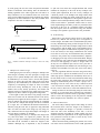
Since a hacker has knowledge of the chip timing, a hacker
also has enough knowledge of the chip to know when data
is being stored in a particular register. By exploiting the
ability to switch between functional and test modes, the hacker
can perform two types of attacks based on the scan design
properties of controllability and observability. The first method
of attack begins with the application of a known value to the
primary input of the chip while in functional mode. The hacker
allows functional mode operation to continue until sensitive
data is loaded into registers accessible through the scan chain,
at which point, test mode is enabled. Test mode stops normal
operation of the chip and creates a snapshot of the current
state of the chip, which can be serially scanned-out with the
help of the scan chain. By repeating this process and analyzing
each response scanned-out, a hacker can target the location of
a register in the scan chain and use this to reverse engineer the
technology used in the design or a vital key in a cryptochip.
This process is summarized in Figure 2(a). Since this attack
is based on the ability of the hacker to observe chip operation
and behavior using the scan chain, we will refer to this as a
scan-based observability attack.
The second method of attack is based on both controllability
and observability properties of scan-based designs. The scan
chain provides an easily accessible entry-point for a faultinjection attack [12][13]. The hacker begins this attack with
the chip in test mode in order to apply a random pattern into
the scan chain. By applying random patterns, random faults are
exposed potentially bypassing security measures and changing
necessary registers. Through the analysis of functional mode
when faults are introduced and when no faults are present,
the hacker is able to deduce various properties about the chip
as was done in [13] to find the secret key of a cryptochip.
A summary of this attack is shown in Figure 2(b). This
method of attack is based on controllability and observability
provided by test and we will refer to this as a scan-based
controllability/observability attack.
Testability and security have what appears to be a mutually
exclusive relationship. It is very difficult to satisfactorily meet
the needs of both specifications. A middle ground must be
met between the fully controllable and observable CUT and a
black box. If one takes into consideration the hacker, a clearer
relationship between testability and security can more easily
be concluded. If the designer can target specifically which
Normal Mode
Operation
Input stimuli
Scan Mode
Operation
Take snapshot
Analyze
Scanned−out
Response
Collected Enough
Data
Steal IP/
Secret Key
Generate
New Input
(a) Scan-based observability attack.
Generate
New Input
Snapshot
Scan Mode
Operation
Input Pattern/
Take Snapshot
Input
Pattern
Analyze
Scanned−out
Response
Normal Mode
Operation
Collected Enough
Data
Steal IP/
Secret Key
(b) Scan-based controllability/observability attack.
Fig. 2.
Summary of the steps necessary to perform a successful scan-based attacks.
class he would like to prevent access to, it may be easier to
make design compromises between testability and security. For
example, knowing that the designer would like to prevent their
IP from being accessed by an independent hacker assuming
they do not have a high powered electron microscope at their
disposal, the designer can make use of built-in self-test (BIST)
on vital sections of the circuit while still using conventional
scan test for the remainder of the design. This method will
still retain high coverage for the scan tested areas, but suffer
slightly in the BIST tested sections [3]. The designer sacrificed
testability for security, but was able to target the design of the
chip by qualitatively defining the importance of testability and
security.
III. P RIOR W ORK
Implementing encryption algorithms in hardware have revealed quite a few methods to discover the secret keys
through side-channels. These side-channel attacks include
differential power analysis [10], timing analysis [11], faultinjection [12][13], and most recently scan chain hijacking as
demonstrated in [14]. It is also possible to reveal proprietary
information through these side-channel attacks making these
a particularly large concern to companies.
Due to the side-channel attacks, a lot of attention has begun
to be paid toward the inclusion of security during design. [4],
[6] and [7] discuss the importance of using tamper resistant
design to prevent such side-channel attacks. A VLSI design
flow was proposed by [8] that included designing tamper
resistant circuits beginning as early as the RTL stage.
Traditional side-channel leaks have often been secured with
the use of additional circuitry. Power analysis attacks can
be prevented with noise inducing circuitry [10] or applying
additional circuitry to hide supply variations [20]. Timing
attacks can be prevented by adding additional gates so all
operations are performed in the same amount of time or to add
random delays to processing time [11]. Finally fault-injection
attacks can be detected with additional logic that performs the
inverse operation of the original logic to check if the result
reproduces the input [21][22].
There has not been much work done that is directly related
to the security of scan chains. A traditional method, which
has become popular in smart card security, has been to blow
polysilicon fuses that interrupt interconnects to the test ports or
directly in the scan paths. However, it has been shown that the
fuses can be reconnected with minimally invasive techniques
[23]. There is also the option to completely cut off the test
interface with a wafer saw [24]. Either option eliminates any
possibility for in-field testing. Most have gotten around the
concern by using BIST. In [9], Hafner et al. used BIST to
test the entire cryptochip they designed. It provided high fault
coverage for both the standard cells and memories, but did not
fair nearly as well on the custom designed portions of the chip.
Both BIST and boundary scan were used in [25]. The fault
coverage still was not nearly as high as what could have been
achieved with automatic test pattern generation (ATPG) for
scan-based design. Any security sensitive I/O were excluded
from the boundary scan and it was not specified how such I/O
were tested.
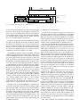
Subchain 1
EN 1
Subchain 2
EN 2
m−to−1
Subchain 3
SO
EN 3
Subchain m
EN
m−bits wide
SI
TC
CLK
Reset
FSM
Test Key
Comparator
m
q−bits wide
Decoder (q−to−m)
LFSR (q−bits wide)
Test Security Controller (TSC)
Fig. 3.
Architecture of Lock & Key security measure.
Recently, work has begun to secure scan designs without
completely destroying access to the test interface. An encoding/decoding security scheme has been presented as a potential
solution in [16] and [17]. More developed solutions have been
published in [15], [26], and [27]. Hély et al. [15] present
a method to prevent invasive and semi-invasive attacks by
modifying the scan chains to internally scramble the values if
the test mode was not properly secured. In order to do so, Hély
proposed splitting up the scan chain into segments that connect
to some other segments in the scan chain. By using a random
number generator, the segments would internally scramble
the contents of the scan chain making the output difficult
to decipher. However, since scan segments are connected
together, as the subchain length decreases, this technique will
create significant logic and routing overhead. Yang et al.
[26] proposed a method that only prevents access to sensitive
registers during test mode. With the use of a mirror key register
(MKR), they were able to remove the encryption key of an
AES hardware implementation from the scan chain while the
chip was set to insecure mode. While this method works
effectively to hide the secret key, it only provides security for
special registers and not the entire scan design. This method
also requires a modification to the JTAG Standard [28] in order
to be effective. Finally, in [27], the authors present a scan
chain content control scheme. The content of the scan chain is
translated into a signature that will be compared to a “golden
signature.” When the two signatures match, the scan chain
functions properly, but if the signatures do not match, a system
wide reset occurs erasing all dynamic memory elements in the
chip.
IV. L OCK & K EY T ECHNIQUE
The Lock & Key security technique can be used to secure
both single and multiple-scan designs. For either case, the scan
chain can be divided into smaller subchains of equal length.
Test vectors are not sequentially shifted into each subchain but
rather a linear feedback shift register (LFSR) performs pseudorandom selection of a subchain to be filled. Figure 3 shows
a general architecture for the Lock & Key method for single-
scan design. This technique proposes a compromise between
testability and security since the LFSR during insecure mode
will protect the scan chain, but also requires an non-sequential
scan chain access when the user has also been verified.
This method prevents correct scan chain manipulation without the presence of a valid test key. This is ensured by
the test security controller (TSC), which consists of four
main components: a finite state machine (FSM), test key
comparator, LFSR, and decoder. There are two states the TSC
can be in: secure and insecure modes. Secure mode signifies
that a trusted user is accessing the scan chain, so the TSC
will select subchains in a predictable, non-sequential order.
Insecure mode signifies a state where the user attempting to
access the scan chain is considered untrustworthy until deemed
otherwise with a correct test key. Unless the test key is entered
and confirmed to be correct, the TSC will unpredictably select
subchains, using the LFSR, to scan in and out; presenting the
user with false information about the scan chain.
A test engineer must perform two steps before entering a
test vector into the scan chain for the first time. After enabling
TC for the first time after a system reset occurs, the TSC
controls all function of the subchains until an authorized or
unauthorized party is detected. A test key must be the first
pattern fed into the TSC. During the first cycles after TC
has been enabled, the first -bits applied to SI will be serially
passed to the test key comparator and checked. After the cycles, the FSM will receive the result. If the key matches
the test key stored in a small secure register, the secure signal
will be raised allowing the TSC to begin operation in secure
mode, which it will remain in until the CUT is reset. If the
secure signal remains low, operation in insecure mode will
resume. If the test key passes and the TSC enters secure mode,
the test engineer then has the ability to seed the LFSR with
a known seed in order to predict the order the LFSR will
select the subchains. Otherwise, the LFSR will work with the
unpredictable random seed created in the LFSR right after a
system reset.
With the LFSR seeded, operation of the scan chain can
begin. Using a decoder to interface between the LFSR and the
EN1
To SI of subchains
EN2
ENm
TSC
SI
secure
TC
Clk
tkc_clk
Decoder (q−to−m bits)
FSM
Reset
Fig. 4.
Test Key
Comparator
Select (q−bits)
test_key/seed
secure
lfsr_clk
LFSR (q+r bits)
Test security controller (TSC) design scheme.
subchains, the TSC uses a one-hot output method to enable one
subchain at a time to read from SI. The output of the LFSR
is also directly connected to the multiplexer selector bits to
allow the data from the subchain to pass to SO. Assuming the
length of each subchain is -bits long, after clock cycles, the
LFSR will shift to a new value and the decoder will disable the
currently active subchain and select a new subchain to read
from SI. After cycles, where is the total
number of subchains and is the total length of the scan
chain, the full length of the scan chain has been initialized
with the first test vector. TC can again be set to zero to place
the CUT into normal mode for one cycle to allow the pattern
to propagate and capture the response back into the scan chain.
When the CUT has returned to test mode, a new test vector is
scanned into the subchains while scanning out the response.
Since test key verification is a one time startup check,
a failed test key causes the TSC to remain in an insecure
mode until the CUT is reset. This essentially locks the scan
chain from being used correctly for the duration of the testing
process. This locking mechanism is also fairly transparent to a
hacker since without prior knowledge of the security scheme,
the chip would appear to be working as it should while still
giving the hacker false data.
A. Design of Lock & Key
The Lock & Key technique depends on the design of
the TSC, which is composed of four components. The FSM
controls the behavior and current mode of the TSC; the test
key comparator is only used when TC is enabled for the
first time returning a secure or insecure result; the LFSR
selects a single subchain during scan operation and controls
the output multiplexer; and the decoder translates the output
of the LFSR into a one-hot enable scheme. Figure 4 shows the
signals passed between each of the components of the TSC.
Communication between each of the components is kept to a
minimum to reduce routing and overall size of the TSC.
The FSM consists of simple state logic and two counters.
The state logic sends control logic to the test key comparator
and LFSR. The FSM also determines, upon the response of the
test key comparator, whether to seed the LFSR with a vector
from SI or to use the random seed created in the LFSR by the
system reset. The first counter is a "! counter used only
for seeding the LFSR, where is the length of the LFSR. The
second counter is a #$ ! counter used for clocking the LFSR
after cycles, shifting the contents of the LFSR to enable a
new subchain.
The test key comparator is used once only after the system
has been reset and put into test mode for the first time. In order
to keep the comparator small and since the test key from SI is
read serially, each bit is serially checked against the key being
stored on chip in a secure register. As each bit is compared, a
FF stores the running result, which will eventually be read by
the FSM. After cycles, the final result will be read by the
FSM determining whether the TSC will run in secure mode
or continue in insecure mode.
When designing the Lock & Key technique, the goal is to
have the ability to ensure security of the scan chains while
maintaining simplicity and design independence. To prevent
the decoder from becoming too complex, an LFSR with a
primitive polynomial configuration will allow the selection of
%'&(*),+ subchains, where is the size of the LFSR
in secure mode. Using a primitive polynomial allows the
selection of all subchains once and only once during a test
round. If a non-primitive polynomial configuration is used,
unless additional logic is included, some subchains may be
selected more than once or never selected at all. Using the bits from the LFSR, the decoder enables one of outputs
leaving the others at zero. Since there is at least one primitive
polynomial for all values of , the LFSR is guaranteed to
choose each subchain once before repeating for any length of
the LFSR [3].
The number of FFs in the design before scan insertion does
not necessarily need to be evenly divisible by . There are
two possibilities to resolve this issue. The first is the inclusion
of dummy FFs, which has become a common practice when
dealing with delay testing [3] and can also be applied to this
technique. If the total number of FFs, , the total number of
dummy FFs, -/.
. , needed is noted in Equation 1.
-/.
. 021
2):;467<=!
, when 3546$768!9
, otherwise
1
(1)
The second option would be to pad portions of the test
pattern that are related to the shorter subchains. This would
immediately shift out any dummy values at the beginning
EN1
KL MN OP
EN2
ENm−1 ENm
Decoder (q−to−m bits)
LFSR (q + r bits)
Insecure Mode Bits
(r−bits)
U
secure
(from FSM)
U
U0
1
TCS TS
R
Q
R
Q
R
Q
EF GH ICIJ
LFSR Used in Insecure Mode
Primitive Polynomial (q−bits)
>? @A BCBD
LFSR Used for Secure Mode
Fig. 5.
Modifiable LFSR determined by security mode of TSC.
of the pattern and would have no effect on the functional
operation of the CUT. This option requires less design effort
since it does not use additional logic but does add overhead to
the test pattern. However, due to test compression techniques,
the overhead would be minimal since the dummy values can
be set to values that maximize compression.
The choice of a primitive polynomial significantly simplifies
the design of the decoder. The decoder can directly translate
the output of the LFSR into a run of zeros and single one to
directly control each subchain. This method not only shortens
design time, but also reduces the area overhead of the TSC
as a whole since additional logic is not needed to ensure all
subchains are selected once during a test round.
The problem with using a primitive polynomial configured
LFSR is the predictability of its behavior. If the LFSR were to
remain unchanged for insecure mode operation, determining
the order would not take long since the order is always the
same, only the start and end points would differ. To avoid this
predictability, the LFSR configuration must be altered when
set to insecure mode. By modifying the LFSR to incorporate
an additional V -bits for insecure mode operation, the primitive
polynomial LFSR becomes a non-primitive polynomial LFSR.
As can be seen in Figure 5, the additional bits are hidden
behind a multiplexer and only become active for insecure
mode operation. The interface between the LFSR and the
decoder is not affected. Since the original LFSR only makes
up a smaller part of the insecure mode LFSR, repetitively
selecting the same subchain multiple times during one test
cycle becomes possible, which results in a more complex
output. A shorter periodicity is not a concern as it was in
secure mode since all subchains do not need to be accessed,
but the facade of a fully functional scan chain still exists.
Algorithms such as the Berlekamp-Massey algorithm [29]
also raises security and complexity concerns of using an LFSR.
The algorithm requires knowledge of the output bit-stream
from the LFSR. However, both the specific values of the
bit-stream (LFSR polynomial) and length of the LFSR are
not directly accessible through I/O pins and contribute to the
complexity as addressed in Section V. If LFSR linearity is still
a security concern, due to the modular nature of the TSC, the
LFSR could be replaced with a non-linear solution at the cost
of additional overhead.
B. Modification to Scan Subchains
In order for the Lock & Key technique to be effective, an
enable signal must be used for each subchain. We cannot treat
the enable signal as TC since that would place one subchain
into test mode while the remaining subchains are in normal
mode, potentially changing all registers that have already been
loaded with a new test vector. We introduce two potential
solutions that avoid modification of the standard scan cell.
The Clock Gating method has been proposed for low power
testing in the past [30][31]. We would like to apply the same
principle to halt normal operation of the subchains when the
enable signal from the TSC is low. In order to do so, this
method adds an additional gate that combines the system clock
and the enable signals from the TSC to the subchain clock.
When the enable signal is high for a particular subchain, the
subchain will behave as a normal scan chain with respect to the
system clock. When the enable signal is low, the subchain will
ignore the system clock and not shift when TC is high. Figure
6(a) shows a gating technique that uses the system clock and
the TSC enable signal. By adding the AND gate as shown in
Figure 6(a), when the respective EN signal for the subchain
is low, the clock signal for each of the SFFs in the subchain
will continue to see a steady-state low and will not register
new values into the FFs.
Since this is a small addition, chip area is not severely
impacted. It does however affect clock skew and chip performance. This solution is not suited for high performance
applications, but does provide the opportunity for low power
testing since at most scan cells would be in transition at any
time as opposed to the full length of the scan chain 3= ! .
Subchain Feedback is the second technique that can be
used to avoid simultaneous normal and test mode subchain
operation. Figure 6(b) shows an example of the subchain
feedback loop. Unlike clock gating, each subchain still shifts
the SFF registers regardless of whether enable is high. By
adding a multiplexer to the input of the subchain, the next
value to be scanned in can either be from the new test vector
if enable is high or from the last register of the subchain
when enable is low. Since we assume that the length of each
subchain is the same in the Lock & Key technique, the data
in each subchain will be maintained after all other subchains
have been scanned.
This option eliminates the performance problem created
by clock gating, but does not reduce the potential maximum
number of transitions when shifting. Since all subchains are
shifting regardless of the enable signal, there will still be as
many transitions as if one continuous chain were used. There
is the need for additional routing for the feedback loop and the
multiplexer, but these additions are still fairly minimal when
compared to the scale of modern designs.
SI
Subchain
SO
TC
clk
EN
(from TSC)
D. In-Field Testing
(a) Clock gating modification
0
SI
Subchain
1
EN
TC
(from TSC)
to split each scan chain into enough subchains that would
maintain the complexity of the Lock & Key technique. The
second option implements the Lock & Key technique on
a different portion of the multiple-scan design. Rather than
affecting the scan chains, the enable signals from the TSC are
used to affect the configuration of the signature register. The
signature mask would unpredictably change while in insecure
mode but still follow a predictable manner when in secure
mode. Implementing Lock & Key in this way would not affect
the design of the TSC in a significant manner and rather
than the response from the scan chains being more difficult
to interpret, the signature register becomes less predictable.
SO
clk
(b) Subchain feedback modification
Fig. 6. Subchain modification techniques necessary to allow Lock & Key
control.
C. Multiple-Scan Chains Design
When applying our Lock & Key technique to multiple-scan
chain designs, essentially the same principles as single scan
designs can be upheld. Multiple-scan chain design provides
an additional layer of security since a decoder and signature
analyzer are used at the input and output of the scan chain,
respectively. This additional layers of hardware increases the
complexity of interpreting the output for those not familiar
with VLSI testing. Including the Lock & Key technique
enhances the security already provided by the decoder and
signature analyzer to further alter the output from being easily
interpreted by those without an appropriate background.
If the length of each scan chain is long enough, each scan
chain can be broken into subchains and the Lock & Key
technique can be applied as shown in Figure 7. Since each scan
chain in multiple-scan designs would normally be controlled
by the same TC, multiple-scan designs can still be controlled
by a single TSC. No additional side-channel information is
leaked by using the same TSC as opposed to using individual
TSCs for each scan chain in the design. By only using one
TSC, differences between single and multiple-scan designs on
the Lock & Key technique are minimal.
When applying Lock & Key to multiple-scan designs with
very short scan chains, two options are possible. The first
option is to apply the technique as normal and break up each
scan chain into subchains no matter the length of each
subchain. Although easy to implement, it may be difficult
Being able to test mission critical devices in the field has
become very difficult with the high level of integration in
modern designs. The IEEE 1149.1 JTAG Standard [28] allows
not only manufacturing testing of these designs, but also infield testing. The Lock & Key technique adapts well to in-field
testing practices and the IEEE 1149.1 JTAG Standard. Since
our technique requires an authorization step before proper use
of the scan chain(s) in the design, unauthorized users would
not be able to access any vital information easily and authorized users can perform any needed maintenance, diagnosis,
or debugging of the chip with conventional methods. Designs
with Lock & Key only require the same modifications needed
of scan test when applying it to JTAG. A design with Lock
& Key have no additional pins and no fewer pins than a
design implemented with standard scan test allowing an easy
transition from standard scan to the more secure Lock & Key
scan test.
The only significant difference between using Lock & Key
for in-field test as opposed to standard scan test is the scan
chain setup process. Standard scan immediately allows use of
the scan chains in the CUT after test initialization. When using
the Lock & Key technique, after initialization, the CUT must
undergo an authorization process to ensure a proper user is
attempting to test the CUT. If the test key is authorized, then
a test seed must be inserted. Only after these two steps can
the test vector be inserted as it would with standard scan test.
Design overhead for in-field testing using the Lock & Key
technique is no more than that of standard scan techniques.
Also, the additional overhead created by appending a test key
and test seed to the beginning of the test pattern is minimal
when compared to the cumulative size of the test pattern.
E. Industrial DFT Flows
The Lock & Key technique requires little change to current
DFT insertion flows. Since the design of the subchains is
similar to multiple-scan design, it is possible to follow the
same flow. Due to the modularity of the TSC, it can be
designed separately and added as another module after scan
insertion and layout optimization on the targeted design has
been performed. Overall, the affect of Lock & Key on the
design aspect is fairly minimal.
When concerned about generating test patterns, the correct
scan order must be defined based on the LFSR polynomial
SI1
SI2
]/^/] ^/] ^/] ^/] ^]
Decoder
SIi
SO 2
W/Y/WXYZ
/[ [\
Signature Analyzer
SO 1
SO
SO i
TC
Clk
Reset
Fig. 7.
TSC
Application of Lock & Key to a multiple-scan chain design.
and the initial seed. This information can be defined in the
test protocol file, which is needed by the ATPG tool for scan
chain information. From the perspective of the ATPG tool, it is
a single scan chain since the order can be arbitrarily assigned
based on a number of design factors. So, industrial ATPG tools
like TetraMax [32] are unaffected by this change.
Although the ATPG tool is not affected by Lock & Key, not
all pattern application techniques are unaffected. Since there
are different methods of performing delay fault testing such
as launch-off-shift (LOS) [33], launch-off-capture (LOC) [34],
and enhanced scan [35], we acknowledge that Lock & Key
does not successfully work with LOS. However, this is not
a major concern since the more widely practiced method of
delay test in industry, LOC, can be successfully applied to our
technique. With that in mind, Lock & Key can be considered
the same as applying scan to a design. All of the same signals
as scan design are used without any change to their function.
V. A NALYSIS
OF
L OCK & K EY
Overall, the Lock & Key technique significantly increases
the amount of work necessary to mount an attack on the
scan chains. A hacker must perform the following tasks to
successfully complete the attack and steal the chip IP:
1) Hackers must first learn of what security strategy is being
used.
2) If they figure out the strategy used, then they must find
the secret test key for operation of the chains to be
predictable. The complexity of the key is completely
dependent on the length, so with a sufficiently long key,
stumbling across the correct key out of &$_ possibilities
becomes quite unlikely.
3) Even if hackers were to be able to discover the test key,
hackers must also determine the pseudo-random order
that patterns will be scanned in and out by determining
the configuration of the LFSR. The number of configurations the LFSR can potentially be placed in for secure
mode is &( and for insecure mode is &`(a
b .
4) In cases where multiple-scan designs are used, hackers
must also account for the additional layers of security
provided by the decoder and signature register.
5) If hackers are able to find all this information, an attack
can finally be mounted against the CUT while still
having to manage with the pseudo-random selection of
the subchains.
A. Complexity Analysis
The number of subchains needed completely depends upon
the amount of complexity required to deter hackers. If there are
subchains in the design, the response scanned out on SO can
be one of dc possible combinations when in secure mode or at
most one of 8e combinations when in insecure mode. With
as few as 15 subchains, an untrusted user that does not have
knowledge of the LFSR configuration nor the seed would have
more than one trillion unique combinations to choose from
in secure mode and more than +gf$hCi possible combinations
to choose from in insecure mode. A brute force attempt at
resolving the pattern to the location in the chain becomes
extremely difficult and continues to increase in difficulty as
increases.
As discussed in Section II, it is easier to design a chip when
a specific hacker class is targeted. The benefit of Lock & Key
security is that it scales easily to the amount of security the
designer would like to include. A small TSC with a 4-bit LFSR
would be more than suitable to stop a beginner, but increasing
the LFSR to 8-bits would potentially be sufficient to prevent
some independent hackers from intrusion. As the granularity
of each subchain becomes smaller and the number of bits in
the LFSR becomes greater, the amount of security and number
of subchain permutations become greater. Table I shows how
well we expect the Lock & Key technique to hold up against
a scan-based attack from the four hacker classes we presented
in Section II. Any minimal implementation should be able
to stop a beginner due to their lack of knowledge. As the
hacker’s knowledge increases, the amount of complexity must
also increase, however, no matter the complexity, government
hackers can only be slowed down and never completely
stopped.
B. Timing Overhead
Considering the size of test patterns for modern designs,
the additional time inserting a test key and test seed do not
TABLE I
L OCK & K EY AGAINST HACKER CLASSES .
Beginner
Independent
Business
Government
Low
X
Complexity
Med
High
X
X
X
X
X
prolong test time by an exorbitant amount. Only the initial
setup placing the TSC into secure mode affects test time. After
test mode has been properly secured and setup, testing the
CUT is no different from standard scan test. The total test
time (j ) would take
(2)
jkml#3=onk+g!pq
rts eutv nk:w= !xnyzn{$|
where is the number of subchains, is the length of each
subchain, rts
eu is the number of combinational vectors, is
the size of the test key, and is the size of the LFSR. The
significance of and decreases as }d and the number
of test rounds increase. With insignificant and values, the
test time becomes solely dependent upon }~ and rts .
eu
Since ' is the total length of the scan chain, we can
replace it with simplifying the equation further making
the total test time no different for the Lock & Key technique
from traditional scan test.
jkm:=on+!pq
rts eu k
n :w= !
jkm: nk+g!p
rts eu
n (3)
(4)
C. Area Overhead
We synthesized our Lock & Key technique in Verilog using
Synopsys’ Design Analyzer tool [32]. Table II shows the
number of equivalent gates returned by Design Analyzer for
the FSM, test key comparator, primitive polynomial configured
LFSR, and decoder with 4-bit, 8-bit, and 12-bit LFSRs. The
total size of the Lock & Key method along with overhead
percentages for ISCAS’89 benchmarks s38417 and s38584.
The Lock & Key test security controller grows fairly slowly
for a large increase in the number of subchains. The FSM
and test key comparator remain a fairly constant size. FSM
operation is mostly independent of size of the LFSR. The test
key comparator is only dependent upon the size of the test key.
1
For a minimally secure test key length, a length of
bits should be used. For our implementation, we used a " -bit
test key. The size of the test key comparator in Table II does
not include the additional overhead for on-chip key storage,
but we did include it in the final size of the TSC. Only the
growth of the LFSR and decoder significantly affect the size,
but the number of subchains that can be used exponentially
increases with each additional bit. The total size of each LFSR
includes the V -bits used for insecure mode operation. We chose
to use a constant V value of for all implementations and the
primitive polynomials used were from [3]. A fair comparison
to other works [15][26][27] cannot be made due to the authors
not providing overhead information of their techniques or
performing their analysis different benchmark designs.
A -bit LFSR can control 15 subchains placing any one of
+gf`hi different subchain combinations on SO while insecure.
Without prior knowledge, a beginner would have little chance
of hacking any vital information from the chip using the
scan chain alone. By doubling the size of the LFSR to bits, most independent hackers and small businesses should
be deterred with the exponential increase in the number of
subchains and security. Increasing the LFSR size again will
greatly increase the amount of security, but at the cost of a
much larger area overhead due to the exponential
growth of the
1
decoder. Increasing the size beyond + -bits risks producing a
fairly large overhead for a level of security that an -bit LFSR
may adequately provide.
Regardless of the size of the LFSR, if business or government hackers have enough resources to open the package
and reverse engineer the layout, any effort to secure the scan
chain is inadequate, which is common for any individual
side-channel countermeasure. However, we suggest that design
engineers use multiple design security techniques to force both
business and government hackers to spend more time, money,
and other resources to eventually make the costs outweigh any
gains.
The components for the TSC are fairly standard and testing
it with BIST can provide a fairly high coverage. Using scanbased testing would result in the side-channel exposure that
the Lock & Key technique tries to protect since it could be
used to expose either the test key or random seed. The other
option would be to simply not test the TSC logic at all since it
is part of the testing logic for the CUT. This option is similar
in nature to the choice of ignoring to test BIST logic due to
the fact that if the CUT returns an incorrect result, the chip is
faulty regardless of whether the CUT is faulty or the TSC is
faulty [3].
VI. C ONCLUSION
Scan-based designs have been proven to be a significant
security risk to the contents of a chip. Without proper security
in place, encryption algorithms can be weakened and IP can
be stolen. We have proposed the Lock & Key technique as a
countermeasure to the method that has been used to expose
vital information through the scan chain. Unless the user is
trusted, our technique will cause the scan chain to operate
unpredictably and make exploitation very difficult. Design of
the technique is flexible and straight forward to implement for
varying degrees of security. Until another method of testing
a chip can yield the similar coverage as scan based designs
with better security, flexible, low-overhead solutions must be
included in the design of scan.
R EFERENCES
[1] Y. Zorian, E. J. Marinissen, and S. Dey, “Testing Embedded-Core Based
System Chips,” in Proc. of Intl. Test Conf., 1998, pp. 130–143.
[2] Y. Zorian, S. Dey, and M. Rodgers, “Test of Future System-on-Chips,”
in Proc. of Intl. Test Conf., 2000, pp. 392–398.
[3] M. L. Bushnell and V. D. Agrawal, Essentials of Electronic Testing.
Kluwer Academic Publishers, 2000.
TABLE II
N UMBER OF GATES IN TSC FOR 4- BIT, 8- BIT, AND 12- BIT.
Number of
LFSR Bits :"!
4-bit LFSR
8-bit LFSR
12-bit LFSR
Size of
FSM
113
133
153
Size of Test
Key Comparator
54
54
54
Size of LFSR
nV"!
48
71
91
[4] R. Anderson and M. Kuhn, “Tamper Resistance - A Cautionary Note,”
in Proc. of The Second USENIX Workshop on Electronic Commerce,
Nov. 1996, pp. 1–11.
[5] ISO/IEC 15408, “Common Criteria for Information Technology
Security Evaluation v2.2,” Jan. 2004. [Online]. Available:
http://www.commoncriteria.org
[6] S. Ravi, A. Raghunathan, and S. Chakradhar, “Tamper Resistance
Mechanisms for Secure Embedded Systems,” in Proc. of the 17th Intl.
Conf. on VLSI Design, 2004, pp. 605–611.
[7] P. Kocher, R. Lee, G. McGraw, A. Raghunathan, and S. Ravi, “Security
as a New Dimension in Embedded System Design,” in Proc. of the 41st
Annual Conference on Design Automation, June 2004, pp. 753–760.
[8] K. Tiri and I. Verbauwhede, “A VLSI Design Flow for Secure SideChannel Attack Resistant ICs,” in Proc. of Design, Automation and Test
in Europe, Mar. 2005, pp. 58–63.
[9] K. Hafner, H. C. Ritter, T. M. Schwair, S. Wallstab, M. Deppermann,
J. Gessner, S. Koesters, W.-D. Moeller, and G. Sandweg, “Design and
Test of an Integrated Cryptochip,” IEEE Design and Test of Computers,
pp. 6–17, Dec. 1991.
[10] P. Kocher, J. Jaffe, and B. Jun, “Differential Power Analysis,” in Proc.
of the 19th Annual Intl. Cryptology Conf. on Advances in Cryptology,
1999, pp. 388–397.
[11] P. C. Kocher, “Timing Attacks on Implementations of Diffie-Hellman,
RSA, DSS, and Other Systems,” in Proc of the 16th Annual Intl.
Cryptology Conf. on Advances in Cryptology, 1996, pp. 104–113.
[12] D. Boneh, R. A. Demillo, and R. J. Lipton, “On the Importance of
Checking Cryptographic Protocols for Faults,” Proc. of Eurocrypt ’97,
pp. 37–51, 1997.
[13] E. Biham and A. Shamir, “Differential Fault Analysis of Secret Key
Cryptosystems,” in Proc. of the 17th Annual Intl. Crytology Conf. on
Advances in Cryptology, 1997, pp. 513–527.
[14] B. Yang, K. Wu, and R. Karri, “Scan Based Side Channel Attack on
Dedicated Hardware Implementations of Data Encryption Standard,” in
Proc. of the IEEE Int. Test Conf. (ITC), 2004, pp. 339–344.
[15] D. Hély, M.-L. Flottes, F. Bancel, B. Rouzeyre, N. Bérard, and M. Renovell, “Scan Design and Secure Chip,” in Proc. of the 10th IEEE Intl.
On-Line Testing Symposium, 2004, pp. 219–224.
[16] R. Goering, “Scan Design Called Portal for Hackers,” Oct.
2004. [Online]. Available: http://www.eetimes.com/news/design/showArticle.jhtml?articleID=51200154
[17] S. Scheiber, “The Best-Laid Boards,” Apr. 2005. [Online]. Available:
http://www.reed-electronics.com/tmworld/article-/CA513261.html
[18] J. Lee, M. Tehranipoor, C. Patel, and J. Plusquellic, “Securing Scan
Design Using Lock & Key Technique,” in IEEE Intl. Symposium on
Defect and Fault Tolerance (DFT’05), Oct. 2005, pp. 51–62.
[19] P. Ludlow, Ed., High Noon on the Electronic Frontier: Conceptual Issues
in Cyberspace, 1st ed. MIT Press, 1996.
[20] G. B. Ratanpal, R. D. Williams, and T. N. Blalock, “An On-Chip
Signal Suppression Countermeasure to Power Analysis Attacks,” IEEE
Transactions on Dependable and Secure Computing, vol. 1, no. 3, pp.
179–188, 2004.
[21] R. Karri, K. Wu, and P. Mishra, “Fault-Based Side-Channel Cryptanalysis Tolerant Architecture for Rijndael Symmetric Block Cipher,” in IEEE
Intl. Symposium on Defect and Fault Tolerance in VLSI Systems, 2001,
pp. 427–435.
[22] R. Karri, K. Wu, P. Mishra, and Y. Kim, “Concurrent Error Detection
Schemes for Fault-Based Side-Channel Cryptanalysis of Symmetric
Block Ciphers,” IEEE Transactions on Computer-Aided Design of Integrated Circuits and Systems, vol. 21, no. 12, pp. 1509–1517, Dec.
2002.
[23] S. P. Skorobogatov, “Semi-invasive Attacks - A New Approach to Hardware Security Analysis,” Ph.D. dissertation, University of Cambridge,
Apr. 2005.
Size of
Decoder
25
307
5432
Total Size
of TSC
327
652
5817
% Overhead
s38417
2.9
5.7
50.8
% Overhead
s38584
3.8
7.5
66.8
[24] O. Kömmerling and M. G. Kuhn, “Design Principles for TamperResistant Smartcard Processors,” in USENIX Workshop on Smartcard
Technology, 1999, pp. 9–20.
[25] R. Zimmermann, A. Curiger, H. Bonnenberg, H. Kaeslin, N. Felber, and
W. Fichtner, “A 177 Mbit/s VLSI Implementation of the International
Data Encryption Algorithm,” IEEE Journal of Solid-State Circuits,
vol. 29, no. 3, pp. 303–307, Mar. 1994.
[26] B. Yang, K. Wu, and R. Karri, “Secure Scan: A Design-for-Test
Architecture for Crypto Chips,” in Proc. of 42nd Annual Conference
on Design Automation, June 2005, pp. 135–140.
[27] D. Hély, F. Bancel, M.-L. Flottes, and B. Rouzeyre, “Test Control for
Secure Scan Designs,” in Proc. of European Test Symposium, 2005, pp.
190–195.
[28] IEEE Standard 1149.1-2001, “Standard Test Access Port and BoundaryScan Architecture,” IEEE Standards Board, Tech. Rep., 2001.
[29] A. Menezes, P. van Oorschot, and S. Vanstone, Handbook of Applied
Cryptography. CRC Press, 1996.
[30] R. Sanakaralingam, B. Pouya, and N. A. Touba, “Reducing Power
Dissipation During Test Using Scan Chain Disable,” in Proc. of VLSI
Test Symposium, 2001, pp. 319–234.
[31] J. Saxena, K. M. Butler, and L. Whetsel, “An Analysis of Power
Reduction Techniques in Scan Testing,” in Proc. Intl. Test Conf., 2001,
pp. 670–677.
[32] Synopsys DFT Compiler, User Manual for Synopsys Toolset Version
2004.06, Synopsys Inc., 2004.
[33] J. Savir, “Skewed-Load Transition Test: Part I, Calculus,” in Proc. of
Intl. Test Conference, 1992, pp. 705–713.
[34] J. Savir and S. Patil, “On Broad-Side Delay Test,” in Proc. of VLSI Test
Symposium, 1994, pp. 284–290.
[35] B. Dervisoglu and G. Stong, “Design for Testability: Using Scanpath
Techniques for Path-Delay Test and Measurement,” in Proc. of Intl. Test
Conference, 1991, pp. 365–374.