1
PIs
POs
Combinational Logic
SI
SO
0
1
0
SFF1
1
0
SFF 2
1
0
SFF 3
1
0
SFF 4
1
0
SFF 5
1
0
SFF 6
1
0
SFF 7
1
SFF 8
TC
Clk
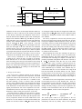
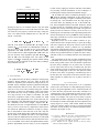
Fig. 1.
An example of a scan chain created from SFFs.
B. Chip Security
Security has become a greater concern in the design and
test of chips recently [4][5][6][7][8]. This has become more
apparent with the advent of cryptochips [9]. Cryptochips
perform encryption and decryption algorithms at the circuit
level. Many researchers have been able to show that these
chips are highly vulnerable to side-channel attacks using
power analysis [10], timing analysis [11], and fault-injection
[12][13]. These attacks are considered non-invasive and if not
considered carefully, strong encryption algorithms that would
take years to crack by brute force can otherwise be crippled
in a manner of weeks, days, or even hours without the need
to disassemble the chip packaging.
Recently, a new vulnerability has been shown to compromise on-chip data. Scan test has been proven a security risk to
the intellectual property (IP) on the chip and has become quite
a concern to the design and test communities [14][15][16][17].
Yang et al. [14] were able to simulate an attack on the scan
chain of a DES cryptochip to reveal the secret key with using
only three plaintexts. Although the scan chains have only been
exploited to find the secret key of a cryptochip, it is just
as easy to uncover proprietary intellectual property through
scan chains since vital registers are part of the chains that
are allowing high controllability and observability. Instead of
simply revealing fabrication defects, the scan chains are also
revealing protected IP.
Currently, the main objective in testing has been to control
and observe a chip as much as possible in order to achieve high
fault coverage and diagnosis on the CUT. As useful as these
properties are for testing, they are completely contradictory to
the objectives of security on a chip. In order to protect a chip
from malicious users, a chip must reveal as little as possible
while still considered useful to the end-user, but for reliability,
a test engineer needs as much access to the chip as possible.
C. Contribution and Paper Organization
In order to prevent IP theft, security measures must be
implemented during the design phase. However, similar to
design countermeasures of the more conventional side-channel
attacks, a design countermeasure from scan-based attacks
would prove futile against an invasive attack.
In this paper, we propose the Lock & Key security technique
in order to prevent aggressive users from maliciously attacking
the scan chains to reveal vital information about the chip using
non-invasive methods [18] and extend the work to include the
effect on DFT industrial flows and test applications techniques.
Our relatively low overhead security solution against scanbased side-channel attacks minimizes the controllability and
observability of the scan chain when an unauthorized user
attempts to access them. The Lock & Key technique divides
the scan chain into smaller subchains of equal length. The test
security controller used by this technique switches between
secure and insecure mode for authorized and unauthorized
users, respectively. When in secure mode, subchain operation
is predictable but non-sequential, but when insecure, subchain
operation is entirely random. This prevents malicious users
from predicting where in the scan chain the stimuli on SI
goes and where the response on SO comes from. The reduced
predictability and random access eliminates repeatability and
prevents reverse engineering.
This paper is organized as follows: In Section II, we will
discuss testability and security as it applies to modern designs
and how the two apply to modern day hackers. Section III
will discuss prior work performed in the field of chip test and
security. We will then propose and discuss our method of Lock
& Key security in Section IV. Section V presents an analysis
of our method. Finally, we will wrap up our discussion in
Section VI with the conclusion.
II. OVERVIEW: T ESTABILITY, S ECURITY
AND
H ACKING
Testability and security inherently contradict each other.
The testability of a chip can be defined by the amount of
controllability and observability the test engineer is granted.
The higher degree of controllability and observability allowed,
the easier it is to test the CUT. The test is not only easier to
perform, but the result of the test becomes more reliable due
to a higher fault coverage.
Security ensures that anything in a circuit is safely stored
within itself. The most common manner of providing security
is to hide the information behind some form of recognition that
would be able to tell a valid user from an attacker. Modern
day security in all realms use this method to protect vital
belongings, whether it is a security code for a home, retinal
scanner for a lab, or encryption key for information. Security
relies on making information obscure and difficult to figure
out.
When trying to relate testability and security together in
chip design, security is clearly contradicted by testability. By
designing for testability, a designer is essentially revealing all
information about the chip through the use of scan test. If the
aim of designing a chip is security, it is very difficult to justify
the amount of controllability and observability that testability