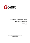
1
LandTiger v2.0
LandTiger V2.0
LPC17XX Development Board
User Manual
Version V1.1
www.PowerMCU.com, www.PowerAVR.com
Copyright © 2009, PowerMCU; Copyright © 2012, WH
LandTiger V2.0 User Manual
2
Table of Content
Table of Content.....................................................................................................................2
1 Overview.............................................................................................................................3
2 Circuit and interface description ..........................................................................................5
2.1 Power supply ................................................................................................................5
2.2 Clock source .................................................................................................................6
2.3 Reset Mode...................................................................................................................7
2.4 Analog Input (ADC) .....................................................................................................7
2.5 Digital Analog Conversion Output (DAC)..................................................................8
2.6 USB-Host .....................................................................................................................8
2.7 USB-Device................................................................................................................10
2.8 Databus Interface ........................................................................................................12
2.8.1 LED Interface ..........................................................................................................12
2.8.2 Conversion Circuit 8bit-16bit ...................................................................................13
2.8.3 Display Interface......................................................................................................14
2.9 EEPROM....................................................................................................................16
2.10 DataFlash..................................................................................................................16
2.11 CAN .........................................................................................................................17
2.12 RS-232......................................................................................................................18
2.13 RS-485......................................................................................................................19
2.14 SD card.....................................................................................................................20
2.15 Ethernet ....................................................................................................................22
2.16 Joystick.....................................................................................................................23
2.17 Switches ...................................................................................................................24
2.18 Reset and Booting .....................................................................................................25
2.19 JTAG Debug Function and JLINK emulator .............................................................27
2.20 External Connector ...................................................................................................29
3 LCD HY-32C, 3.2”, 320x240, 65K colours .......................................................................31
4 Downloading Application Software ...................................................................................34
4.1 In System Programming (ISP) using FlashMagic ........................................................34
4.2 In System Programming (ISP) using the onboard JLink device ...................................35
4.3 In System Programming (ISP) using external JLink devices........................................36
5 Portpin Usage on LandTiger vs mbed ................................................................................38
6 Software compatibility.......................................................................................................42
6.1 Compatibility with Keil ..............................................................................................42
6.2 Compatibility with mbed.............................................................................................42
6.2.1 Hardware .................................................................................................................42
6.2.2 Downloading new application software....................................................................45
6.3 Compatibility with CooCox CoIDE for ARM .............................................................45
7 JTAG Interface Description ...............................................................................................46
7.1 JTAG standard connector for ISP and Debugging .......................................................46
7.2 SWD and SWO/SWV (also called SWV) compatibility ..............................................50
7.3.1 Serial Wire Output (SWO) compatibility..................................................................52
7.3.2 Serial Wire Viewer (SWV) compatibility.................................................................52
7.3.3 Cortex 10 Pin Debug compatibility ..........................................................................52
7.3.4 Cortex 20 Pin Debug compatibility ..........................................................................53
7.3.5 ARM ETM 'Mictor' Connector (38-pin) ...................................................................53
8 References.........................................................................................................................55
LandTiger V2.0 User Manual
3
1 Overview
The LandTiger V2.0 NXP LPC1768 ARM development board is based on a secondgeneration ARM Cortex-M3 microcontroller, a high-performance, low-power 32-bit
microprocessor designed for embedded system applications, suitable for instrumentation,
industrial communications, motor control, lighting control, alarm systems, and other fields.
The board supports USB2.0 Device and Host, dual CAN interfaces, RS-485 interface and an
on-board USB emulator for JLINK. The development board is supported by a rich set of
example software and detailed information to facilitate the users to quickly project
development. A short feature overview:
Powerful LPC1768 MCU Cortex-M3 core:
Clock frequency up to 100MHz.
Includes support of eight areas of memory protection unit (MPU).
Built-in Nested Vectored Interrupt Controller (NVIC).
512KB on-chip Flash program memory, supports in-system programming (ISP) and In
Application Programming (IAP).
64KB SRAM for high-performance CPU access through the instruction bus, system
bus, data bus access.
AHB multi-layer matrix with 8-channel general-purpose DMA controller (GPDMA).
Supports SSP, UART, I2C, I2S, ADC, DAC, Timer, PWM, GPIO, etc., can be used
for memory-to-memory transfer.
Standard JTAG test / debug interface and a serial wire debugging and serial wire
tracking port option.
Simulation trace module supports real-time tracking.
4 low-power modes: sleep, deep sleep, power-down, deep power-down.
Single 3.3V power supply (2.4V - 3.6V).
Operating temperature: -40° C - 85° C.
Non-maskable interrupt (NMI) input.
On-chip integrated power-on reset circuit.
Built-in systems timer (SysTick), to facilitate operating system migration.
Onboard resources:
2 RS232 serial interfaces (using straight-through serial cable), (RS232 Transceiver:
SP3232). One serial port supports ISP download of programs.
2 CAN bus communication interfaces (CAN Transceiver: SN65VHD230).
RS485 communication interface (485 Transceiver: SP3485).
RJ45-10/100M Ethernet network interface (Ethernet PHY: DP83848).
DAC output interface, on-board speaker and speaker output driver (LM386).
ADC input interface, on-board adjustable potentiometer input.
Color LCD display interface (supports 2.8-inch or 3.2-inch color TFT 320X240).
Touchscreen supported through SPI interface.
USB2.0 Interface, USB host and USB Device interface.
SD/MMC card (SPI) interface.
I2C Interface, connected to onboard 2Kbit EEPROM (24LC02).
SPI serial interface connected to onboard 16Mbit Flash (AT45DB161D).
2 user keys, 2 function keys (INT0 and Reset button).
8 LED lights (Digital outputs).
Five-way joystick button (Digital Inputs).
LandTiger V2.0 User Manual
Serial ISP download support (COM0).
Standard JTAG download, simulation debugging interface.
Integrated JLINK compatible emulator (USB): support online simulation and debug
capabilities, support KEIL, IAR and other mainstream development environments.
Optional external 5V power supply or USB input to provide 5V power supply.
Breakout available for all the IOs, user-friendly connection of external application
development circuits.
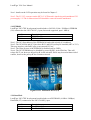
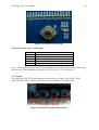
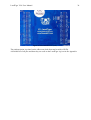
Figure 1 Board Overview (Note: Picture shows version 1.0 of the board)
4
LandTiger V2.0 User Manual
5
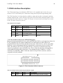
2 Circuit and interface description
Due to the limited space in this manual, please use the circuit schematic reference for
additional details on ICs and specific functions.
2.1 Power supply
The LandTiger development board may be powered by an external 5V power input or by the
USB debug interface 5V power input.
5V DC power adapter connected to CN9, power select jumper JP3 plugged into 1-2
selects the external 5V power supply.
Connecting the PC USB cable to the USB debug port CN4 and power select jumper J3
plugged into 2-3 will choose USB 5V supply. The board will be powered by the PC
USB port (maximum current of 500mA limit).
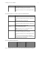
Tabel 1 Jumper settings for powersupply select
Jumper
JP3
Description
JP3 is used to select the external 5V power supply or
USB powersupply.
External 5V power supply: Jumper short1-2
USB-powered: Jumper short 2-3
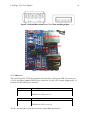
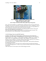
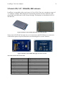
Figuur 2 Powersupply Jumper JP3, connector CN9 and main powerswitch
Main powersupply switch SW6 is provided to switch the board on or off. LED LD11
indicates when the board is powered.
LandTiger V2.0 User Manual
6
Note1: CN9 powerconnector inner pin is positive, outer ring is negative. The input voltage
must not exceed 5V ± 5%. Plug dimensions: 5mm outside, 2.5mm inside.
Figuur 3 External 5V powersupply connector CN 9
Note2: The USB Device port (CN12) can not be used to power the LandTiger board.
Note3: Insert JP1 jumper to connect the onboard battery to the RTC when the board is
disconnected from the external powersupply, when JP1 is open the RTC will only run as long
as power is supplied and not maintain time when switched off.
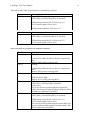
Tabel 2 Jumper settings for RTC powersupply
Jumper
JP1
Description
JP1 is used to connect onboard backup battery to the
RTC.
Battery backup: Jumper inserted
No battery backup: Jumper removed
Figuur 4 RTC Battery Jumper JP1 and batteryholder BT1
Note1: The RTC backup battery type is CR1225 (Lithium, 3V).
2.2 Clock source
The development board has four different clock sources: System clock, Realtime Clock (RTC
clock), Ethernet clock and Debugger interface clock.
Y1, 12 MHz crystal, is the main system clock source, the internal RC oscillator of the
CPU can not be used.
Y2, 32.768 kHz crystal, is the clock source for the RTC.
U4, 50MHZ crystal, is the Ethernet PHY chip DP83848 clock.
LandTiger V2.0 User Manual
7
Y3, 8 MHz is the clock for the JLink Debugger interface
Note 1: See section 2.1 on powersupply and onboard battery backup for the RTC.
2.3 Reset Mode
The reset signal in the Land Tiger LPC17XX development board is active low reset. The reset
modes include the following:
Press Reset button Reset (SW1)
Reset signal is input through the JTAG emulator download.
Reset signal is input through the ISP COM1 port (DTR control).
2.4 Analog Input (ADC)
Adjustable potentiometer VR1 is connected to analog channel P1.31 (AD0.5). JP12 jumper is
used to enable the potmeter input. VR1 setting provides input voltages between 0V and 3V3
to the ADC.
Tabel 3 Jumper setting for Analog Input
Jumper
JP12
Description
JP12 is used to enable the VR1 connection to ADC
input (P1.31 AD0.5).
VR1 Connected to AD0.5: Jumper short
No ADC input: Jumper removed
Figuur 5 ADC Potmeter and Jumper JP12
LandTiger V2.0 User Manual
8
2.5 Digital Analog Conversion Output (DAC)
External speaker circuit is connected to DAC output pin P0.26. The DAC output is enabled by
JP2 jumper. The speaker is driven by an onboard audio amplifier U2 (LM386).
Tabel 4 Jumper setting for DAC output
Jumper
JP2
Description
JP2 is used to enable the external speaker.
Speaker connected to P0.26: Jumper short
No Speaker output: Jumper removed
Figuur 6 Loudspeaker and Jumper J2
2.6 USB-Host
LandTiger LPC17XX development board provides a full-speed USB 2.0 Host port (CN11),
through a standard USB-A Type connector. The USB host port may be used to connect USB
peripherals, such as: USB disk, USB mouse, USB keyboard and other equipment.
Set JP9, JP11 jumpers into 3-4 position for the USB Host interface.
Jumper
JP9
Description
Select USB-D +.
USB host: JP9 set to 3-4
Jumper
JP11
Description
Select USB-D -.
USB host: JP11 set to 3-4
Connected devices should be provided with 5V power. This power is activated under control
of the user program. Note that maximum current is limited.
LandTiger V2.0 User Manual
IO Pin
P1.19
9
Description
Activate USB Host power.
LED LD15 is lit when power is activated.
USB power control by P1.19: control signal is active
low.
Tabel 5 The LPC1768 reserves a number of pins for the USB Host functions.
IO Pin
P0.29
Description
USB_D+
P0.30
Connected to either the Host or Device connector by
JP9
Release P0.29 pin by removing JP9
USB D-
P1.22
Connected to either the Host or Device connector by
JP11
Release P0.30 pin by removing JP11
Sense USB Host power state.
P1.19
USB powersense by P1.22: input signal is active
high.
Release P1.22 pin by removing R78
Activate USB Host power.
LED LD15 is lit when power is activated.
USB power control by P1.19: control signal is active
low.
P1.19 may be used a general purpose output and
LD15 may be used as general purpose indicator when
USB Host functions are disabled.
Tabel 6 CN11 USB AB-type pin functions
Pin
1
2
3
4
Description
VBUS (5V)
DD+
GND
Typical wire colour
Red
White
Green
Black
Note1: The figure shows a front view of the socket (left) and the plug is facing you.
LandTiger V2.0 User Manual
Figuur 7 USB AB Host Connector CN11 (left) and Plug (right)
Figuur 8 USB Jumpers and LEDs
2.7 USB-Device
The Land Tiger LPC17XX development board provides a full-speed USB 2.0 device port
(CN12), through a standard USB-B Type connector. Set JP9, JP11 jumper Plugged into 1-2
position for the USB Device interface.
Jumper
JP9
Description
Select USB-D +.
USB device: JP9 set to 1-2
Jumper
JP11
Description
Select USB-D -.
USB device: JP11 set to 1-2
The D+ line may have a pull-up activated to signal high-speed mode.
10
LandTiger V2.0 User Manual
This pull-up may either be permanent or controlled by software.
Jumper
JP10
Description
Select USB-D + signal pull-up resistor mode.
LED LD14 is lit when the pull-up is activated.
USB pull-up control by P2.9: JP10 set to 1-2
(P2.9 control signal is active low).
USB permanent pull-up: JP10 set to 2-3
IO Pin
P2.9
Description
Activate USB Device pull-up.
LED LD14 is lit when the pull-up is activated.
USB pull-up control by P2.9: JP10 set to 1-2
(P2.9 control signal is active low).
Tabel 7 LPC1768 reserved pins for the USB Device functions.
IO Pin
P0.29
Description
USB_D+
P0.30
Connected to either the Host or Device connector by
JP9
Release P0.29 pin by removing JP9
USB D-
P1.30
Connected to either the Host or Device connector by
JP11
Release P0.30 pin by removing JP11
Sense VBUS from host in USB- Device mode.
P1.18
P2.9
VBUS is active high.
Release P1.30 pin by removing R123.
USB Device is up indicator.
LED LD13 is lit when USB is activated.
(active low)
P1.18 may be used a general purpose output and
LD13 may be used as general purpose indicator when
USB Device functions are disabled.
Activate USB Device pull-up.
LED LD14 is lit when the pull-up is activated.
USB pull-up control by P2.9: JP10 set to 1-2
(P2.9 control signal is active low).
P2.9 may be used a general purpose output and LD14
may be used as general purpose indicator when USB
Device functions are disabled.
11
LandTiger V2.0 User Manual
12
Tabel 8 CN12 USB B-type pin functions
Pin
1
2
3
4
Description
VBUS (5V)
DD+
GND
Typical wire color
Red
White
Green
Black
The figure below shows a front view of the socket (left), the plug (right) is facing you.
Figuur 9 USB B Device Connector CN12 (left) and Plug (right)
Note1: The USB Device port (CN12) can not be used to power the LandTiger board. Power
must be supplied either by the external power connector or by the USB debug port (CN4).
2.8 Databus Interface
The ARM LPC1768 does not have a separate data, address and controlbus. The LandTiger
board is designed to emulate a simple processorbus by using some of the regular port pins.
Port pins P2.0 ... P2.7 represent an 8 bit databus. The datalines are connected to an 8bit - 16bit
conversion circuitry provided by U8 and U9. A number of controllines are also available that
provide /RD, /WR, /CS and /RS. The LPC1768 Resetline is also available.
The main use for the bus is to control an LCD display. However, the design is generic and
may be used to control other peripheral hardware also.
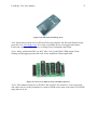
2.8.1 LED Interface
The 8 data lines P2.0-P2.7 are directly connected to a 74LV244 driver (U11) followed by 8
red LEDs (LD4 ... LD11). The LEDs display the current bitpattern on the databus. The LEDs
may be disabled by removing JP8.
Jumper
JP8
Description
Enable databus LEDs.
LEDs enabled: JP8 inserted
LEDs disabled: JP8 removed
Note1: the datalines are shared with the LCD and the LEDs will show any databus activity to
the LCD.
Note2: P2.7 corresponds to LD4 (leftmost), P2.0 corresponds to LD11 (rightmost)
LandTiger V2.0 User Manual
13
Figuur 10 LEDs and Enable Jumper J8
2.8.2 Conversion Circuit 8bit-16bit
The datalines are connected to an 8bit - 16bit conversion circuitry provided by U8 (16bit
bidirectional buffer, 74ALVC164245) and U9 (8bit latch, 74LV573). The tables below show
the steps needed to use the 8-16 bit conversion circuitry for Read and Write operations. There
are 3 specific controllines required for the 8-16 bit conversion unit: LCD_DIR, LCD_EN,
LCD_LE.
Tabel 9 Write operation sequence for 16 bit Databus
Steps
Set P2.0-P2.7 as Output
Set Buffer Direction
to WR
Enable buffer outputs
Latch D00-D07 Transparant
Setup D00-D07
Latch D00-D07
Setup D08-D15
Select Device
Select Data/Control Reg
Write Data (Start)
Write Data (End)
Deselect Device
…
Control/datapin
IO Pin
LCD_DIR=1
P0.21
LCD_EN=0
LCD_LE=1
Write LSBs
LCD_LE=0
Write MSBs
LCD_CS=0
LCD_RS=X
LCD_WR=0
LCD_WR=1
LCD_CS=1
P019
P0.20
P2.0-P2.7
P0.20
P2.0-P2.7
P0.22
P0.23
P0.24
P0.24
P0.22
Tabel 10 Read operation sequence for 16 bit Databus
Steps
Set P2.0-P2.7 as Input
Set Buffer Direction
to RD
Enable MSB buffer outputs
Select Device
Select Data/Control Reg
Read Data (Start)
Control/datapin
IO Pin
LCD_DIR=0
P0.21
LCD_EN=0
LCD_CS=0
LCD_RS=X
LCD_RD=0
P019
P0.22
P0.23
P0.25
LandTiger V2.0 User Manual
Read D08-D15
Enable LSB buffer outputs
Read D00-D07
Read Data (End)
Deselect Device
…
14
Read MSBs
LCD_EN=1
Read LSBs
LCD_RD=1
LCD_CS=1
P2.0-P2.7
P019
P2.0-P2.7
P0.25
P0.22
Tabel 11 Databus interface description
Description
DB00
DB01
DB02
DB03
DB04
DB05
DB06
DB07
DB08
DB09
DB10
DB11
DB12
DB13
DB14
DB15
/CS
RS
/WR
/RD
RESET
IO Pin
P2.0 (latched)
P2.1 (latched)
P2.2 (latched)
P2.3 (latched)
P2.4 (latched)
P2.5 (latched)
P2.6 (latched)
P2.7 (latched)
P2.0 (buffered)
P2.1 (buffered)
P2.2 (buffered)
P2.3 (buffered)
P2.4 (buffered)
P2.5 (buffered)
P2.6 (buffered)
P2.7 (buffered)
P0.22
P0.23
P0.24
P0.25
RESET
2.8.3 Display Interface
The CN7 Databus interface of the Land Tiger LPC17XX development board can be
connected to a 2.8 or 3.2 inch 320X240 TFT color LCD. The datalines are connected to P2.0
... P2.7 and by 8bit - 16bit conversion circuit connected to the LCD.
In addition to the 16 bit databus, the LCD interface also supports a touchschreen controller.
This interface is provided as an SPI bus.
Depending on the LCD board the LCD backlight may be controlled either as on/off or with
variable brightness (PWM control).
The databus/LCD connector pinout is defined in the table below:
LandTiger V2.0 User Manual
15
Tabel 12 CN7 Databus/Color TFT LCD interface description
Pin
1
2
3
4
5
6
7
8
9
10
11
12
13
14
15
16
17
18
19
20
Description
5V
GND
DB00
DB01
DB02
DB03
DB04
DB05
DB06
DB07
DB08
DB09
DB10
DB110
DB12
DB13
DB14
DB15
/CS
RS
IO Pin
Power supply
Ground
P2.0 (latched)
P2.1 (latched)
P2.2 (latched)
P2.3 (latched)
P2.4 (latched)
P2.5 (latched)
P2.6 (latched)
P2.7 (latched)
P2.0 (buffered)
P2.1 (buffered)
P2.2 (buffered)
P2.3 (buffered)
P2.4 (buffered)
P2.5 (buffered)
P2.6 (buffered)
P2.7 (buffered)
P0.22
P0.23
21
22
23
24
25
26
27
/WR
/RD
RESET
NC
BLVCC
BLGND
BLCNT (Brightn.
PWM)
P0.24
P0.25
RESET
NC
5V
GND
NC
28
TP_INT Touchscreen
P2.13
29
30
/TP_CS Touchscreen
TP_SCK
Touchscreen
TP_MOSI
Touchscreen
TP_MISO
Touchscreen
3V3
GND
P0.6
P0.7
31
32
33
34
P0.9
P0.8
3V3
GND
Comment
See Note2
Databus
Low active
RS = 1:
Instruction
Register
RS = 0: Data
Register
Low active WR
Low active RD
Low active
Do not connect
Backlight VCC
Backlight GND
Control of the
backlight
brightness via
PWM
Low level while
the touch screen
detects pressing
Low active
Connects to SPI
SCK
Connects to SPI
MOSI
Connects to SPI
MISO
See Note2
LandTiger V2.0 User Manual
16
Note1: details on the LCD operation may be found in Chapter 3.
Note2: The 5V-3V3 converter on the HY32-C LCD board is interfering with mainboard 3V3
powersupply !!!!! The 0-Ohm resistor R58 should be removed from the mainboard.
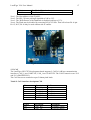
2.9 EEPROM
LandTiger LPC17XX development board includes a 24LC02 (2 kbit / 256kByte) EEPROM
(U6) connected to the LPC1768 I2C_0 port (fast mode supported, upto 1 Mbit/s).
IO Pin
P0.27
P0.28
Description
EEPROM SDA
EEPROM SCL
Note1: The I2C Slaveaddress of the EEPROM is hardcoded at 0xA0 (8 bit address)
Note2: The I2C0 SDA and SCL lines have R121 and R122 pull-up Rs installed (4K7 to 3V3).
This may interfere with Pull-Up Rs on an external I2C bus.
Note3: The Write Protect of the EEPROM is disabled (pull to GND).
Note4: The I2C EEPROM may be disabled by removing R53 in the SDA line. That will
release P0.27 pin, however the pull-up R is still activated. P0.28 may be used without risk of
conflict, however the pull-up R also remains activated.
Figuur 11 I2C EEPROM 24C02 (U6)
2.10 DataFlash
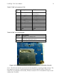
LandTiger LPC17XX development board includes an AT45DB16D (16 Mbit / 2MByte)
DataFlash (U7) connected to the LPC1768 SPI_0 port.
IO Pin
P0.18
P0.17
Description
DataFlash MOSI
DataFlash MISO
LandTiger V2.0 User Manual
P0.16
P0.15
17
DataFlash /CS (active low)
DataFlash SCK
Note1: The Slaveaddress of the FLASH …
Note2: The SPI_CS has a pull-up R installed of 10K to 3V3.
Note3: The /WriteProtect of the DataFlash is disabled (pull-up to 3V3).
Note4: The Flash may be disabled by removing R59 in /CS line. That will release P0.16 pin.
P0.15, P017, P0.18 may be used without risk of conflict.
Figuur 12 SPI Flash 45DB16D (U7)
2.11 CAN
The LandTiger LPC17XX development board supports 2 CAN2.0 A/B bus communication
interfaces. CAN_1 uses UART XX, CAN_1 uses UART XX. The CAN Transceivers are U12
and U13 (SN65HVD230).
The CAN bus screw terminal accepts 5.08mm pitch leads.
Tabel 13 CAN interface description CN8
Pin
1
2
3
4
5
6
IO Pin
P0.0
P0.1
Description
5V
CAN_1 H
CAN_1 L
CAN_2 H
CAN_2 L
GND
Description
CAN1_RX
CAN1_TX
IO Pin
P0.0/P0.1
P0.0/P0.1
P0.4/P0.5
P0.4/P0.5
Comment
CANRX1/TXD3
CANTX1/RXD3
LandTiger V2.0 User Manual
P0.4
P0.5
18
CAN2_RX
CAN2_TX
CANRX2
CANTX2
Figuur 13 CAN1 and CAN2 connector CN8; RS485 Connector CN10
Note1: The CAN1 and CAN2 inputs/outputs are terminated by R129 and R128 (120 ohm).
This means the LandTiger should be located on either end of the CAN bus rather than
somewhere in the middle.
Note2: The CAN1 may be disabled by removing R74 in CAN1_RX line. That will release
P0.0 pin. P0.1 may be used without risk of conflict.
Note3: The CAN2 may be disabled by removing R72 in CAN2_RX line. That will release
P0.4 pin. P0.5 may be used without risk of conflict.
2.12 RS-232
The Land Tiger LPC17XX development board supports two bi-directional RS-232
Communication interfaces COM1, COM2 connected to LPC1768 UART0 and UART2. The
RS232 Transceivers is U10 (SP3232).
The COM1 RS-232 interface may also be used for automatic ISP programming (serial
download program). The port provides two control signals for RESET and ISP activation. The
circuitry is compatible with the ISP standard as defined by NXP. Note: JP6, JP7 jumpers must
be installed to use serial programming procedures.
Tabel 14 COM1 interface description
Pin
1
2
3
4
5
6
7
8
Description
TXD
RXD
DTR
GND
RTS
IO Pin
NC
UART0_TX (P0.2)
UART0_RX (P0.3)
DTR (Control RESET)
GND
NC
RTS
(Control ISP, P2.10)
NC
LandTiger V2.0 User Manual
9
Shield
19
Shield
NC
GND
Tabel 15 COM2 interface description
Pin
1
2
3
4
5
6
7
8
9
Shield
Jumper
JP6
Description
TXD
RXD
DTR
GND
RTS
Shield
IO Pin
NC
UART2_TX (P0.10)
UART2_RX (P0.11)
NC
GND
NC
NC
NC
NC
GND
Description
Enable ISP Select.
Enable ISP Select: JP6 inserted
Disable ISP Select: JP6 removed
Jumper
JP7
Description
Enable ISP Reset.
Enable ISP Reset: JP7 inserted
Disable ISP Reset: JP7 removed
Figuur 14 RS232 connector COM1, COM2 (female, front view)
Note1: The COM1/UART0 may be disabled by removing R70 in UART0_RX line. That will
release P0.3 pin. P0.2 may be used without risk of conflict.
Note2: The COM2/UART1 may be disabled by removing R71 in UART1_RX line. That will
release P0.11 pin. P0.10 may be used without risk of conflict.
2.13 RS-485
The LandTiger LPC17XX development board supports a bi-directional RS-485
communication interface via CN10 to UART3. The 485 Transceiver is U14 (SP3485).
LandTiger V2.0 User Manual
20
Tabel 16 RS485 interface description CN10
Pin
1
2
IO Pin
P4.28
P4.29
P2.8
Description
485A
485B
Description
485_TX
485_RX
485_DIR
IO Pin
UART3_TX (P4.28)
UART3_RX (P4.29)
Comment
TX/RX Direction
(RX is active low,
TX is active high)
Note1: The 458A and 458B inputs/outputs are terminated by R84 (120 ohm). This means the
LandTiger should be located on either end of the RS485 bus rather than somewhere in the
middle.
Note2: The 458A and 458B inputs/outputs do not have pull-up/pull-down resistors to provide
a defined bias idle voltage. These resistors may have to be added externally.
Note3: The 485 interface may be disabled by removing R77 in 485_RX line, that will release
P4.29 pin. Also remove R76 in 485_DIR line to release P2.8. P4.29 may be used without risk
of conflict.
Figuur 15 CAN1 and CAN2 connector CN8; RS485 Connector CN10
2.14 SD card
The Land Tiger LPC17XX development board supports an SD card interface (CN6). The SD
card is accessed through the LPC1768's SSP0 port. A card detection signal is available. The
power supply to the SD card is under control of the LPC17XX.
LandTiger V2.0 User Manual
21
Tabel 17 SD Card connector CN9
SD
Pin
1
Description
IO Pin
/SDcard_CS
2
3
4
5
6
7
8
9
10
11
12
SDcard_DIN
Vss/GND
+3V3
SDcard_CLK
Vss/GND
SDcard_DOUT
NC
NC
/SDcard_detect
GND
NC
P1.21 (SSEL0)
Active Low
P1.24 (MOSI0)
Vss/GND
+3V3 (P3.26 controlled)
P1.20 (SCK0)
Vss/GND
P1.23 (MISO0)
NC
NC
P3.25, Active Low
GND
NC
Tabel 18 SD Card controlsignals
IO Pin
P1.21
P3.26
P3.25
Description
/SDcard_CS, Active Low
SD Power, Active Low
LD3 is lit when power in on
/SDcard_detect, Active Low
Figuur 16 SD card socket (Power on LED LD3 is located on frontside of board)
Note1: The SD card interface may be not be fully disabled by removing 0-Ohm resistors. The
best option is to prevent a card from being inserted. Removing R52 in SD_CS line will
release P1.21 pin. Remove R54 in SD_CD line to release P3.25. P3.26 and LD3 may be used
without risk of conflict.
LandTiger V2.0 User Manual
22
2.15 Ethernet
The LandTiger LPC17XX development board has onboard support for 10/100 Mbit/s
Ethernet communication. The LPC1768 chip supports the RMII interface and links to the
DP83848 (U5) Ethernet PHY chip. This device interfaces out via the RJ45 connector (CN5)
which has internal magnetics and network filters. The RJ45 connector has integrated LEDs to
indicate link connectivity and collisions. A separate LED indicates 10/100 Mbit/s linkspeed
(LD2).
Figuur 17 Ethernet PHY and RJ45 connector
Tabel 19 Ethernet controlsignals
IO Pin
P1.4
P1.0
P1.1
P1.9
P1.10
P1.14
P1.8
P1.16
P1.17
P1.15
Description
ENET_TX_EN
ENET_TX_D0
ENET_TX_D1
ENET_RX_D0
ENET_RX_D1
ENET_RX_ER
ENET_CRS
ENET_MDC
ENET_MDIO
ENET_REF_CLK
LandTiger V2.0 User Manual
23
Figuur 18 RJ45 connector CN5 (frontview)
Tabel 20 RJ45 interface description
Pin
1
2
3
4
5
6
7
8
Shield
Description
TxData+
TxDataRxData+
Shield
Shield
RxDataShield
Shield
Shield
Note1: The Ethernet interface may be not be fully disabled by removing 0-Ohm resistors.
Removing R49, R50 and R51 will release P1.15, P1.16 and P1.17.
2.16 Joystick
The LandTiger LPC17XX board features a 5 way digital joystick (SW5). The joystick may be
used for example to select options in a menu shown on the LCD. Each direction (up, down,
left, right) and the Select function are connected to a dedicated digital inputpin on the
LPC17XX. Multiple keys can be pressed at the same time (e.g. up and right). Inputpins are
active low when a key is pressed. The inputpins are hardware debounced.
LandTiger V2.0 User Manual
24
Figuur 19 Joystick 5-Way Switch
Tabel 21 Joystick 5-way switchsignals
IO Pin
P1.25
P1.26
P1.27
P1.28
P1.29
Description
Select (Active Low)
Down (Active Low)
Left (Active Low)
Right (Active Low)
Up (Active Low)
Note1: The Joystick interface may be fully disabled by removing 0-Ohm resistors. Removing
R65, R66, R67, R68 and R69 will release P1.29, P1.28, P1.27, P1.26 and P1.25.
2.17 Switches
The LandTiger LPC17XX board features 4 switches: Key1 (SW4), Key2 (SW3), INT0
(SW2), RESET (SW1). These switches have several functions. See table below.
Figuur 20 Switches and Alternate functions
LandTiger V2.0 User Manual
25
Tabel 22 Switch Description
Key type
Key1
Key2
INT0
Reset
Description
Connected to INT1 (P2.11),
Active Low, Pull-Up R of 10K
installed.
Connected to INT2 (P2.12),
Active Low, Pull-Up R of 10K
installed.
Connected to INT0 (P2.10)
when JP5 is inserted.
Active Low, Pull-Up R of 10K
installed.
Manual Reset
Comment
SW4
SW3,
Secondary function to enter
the USB ISP mode.
SW2,
Secondary function to enter
the COM1 ISP mode.
SW1
Note1: Key1 may be disabled by removing R64, this will release P2.11.
Note2: Key2 may be disabled by removing R63, this will release P2.12.
2.18 Reset and Booting
The LandTiger LPC17XX development board has several options for Reset and booting.
Tabel 23 Reset and Boot options
Reset type
Power On
Description
The board will reset when
power is applied. The
LPC17XX will boot by
starting the user program
stored in internal Flash (512
KBytes).
Manual Reset The board will reset whenever
the user presses the Reset key.
(SW1) and then behaves just as
after Power-On reset.
Manual Reset The device will enter the ISP
and enter ISP programming mode when
mode
INT0 (SW2) is pressed and
held before applying a Reset.
The device is then ready to
accept and store new user-code
in the internal Flash.
External
Reset
External
The board will reset whenever
DTR is activated on COM1
and then behaves just as after
Power-On reset.
The board will reset and enter
Comment
SW2 is only connected to
INT0 (P2.10) when JP5 is
inserted.
New program download
through COM1 (UART0).
On completion of download,
Reset again to activate the
new code.
DTR is only connected to
Reset when JP7 is inserted.
DTR is only connected to
LandTiger V2.0 User Manual
Reset and
enter ISP
mode
26
the ISP programming mode
whenever DTR is activated
(Reset) and RTS is activated
(ISP) on COM1. The board
then behaves just as like
manually entering the ISP
mode and it is ready to accept
and store new user-code in the
internal Flash.
External
Reset and
enter ISP
mode
Manual Reset
and enter ISP
mode
The device may be Reset and
brought in ISP mode through
the JTAG port.
The device will enter the USB
Secondary bootloader
programming mode when
Key2 (SW3) is pressed and
held before applying a Reset.
The device is then ready to
accept and store new user-code
through the USB device port.
Reset when JP7 is inserted.
RTS is only connected to
INT0 (P2.10) when JP6 is
inserted.
New program download
through COM1 (UART0).
On completion of download,
Reset again to activate the
new code.
New program download
through JTAG.
Key2 is connected to INT2
(P2.12).
The USB Host will detect the
LPC17XX as a mass storage
device holding one binary
file (the current program).
Delete that file and download
a new one through USB.
Reset again to activate the
new code.
Note: a special USB
bootloader must be stored in
Flash first. See NXP
documentation.
Tabel 24 Reset and Boot Jumper settings
Jumper
JP5
Description
INT0 (P2.10)
connected to Key2
JP7
Reset
activated by DTR
JP6
INT0 (P2.10)
activated by RTS
Comment
Insert Jumper to
enable manual
entering ISP mode
Insert Jumper to
enable external
Reset
Insert Jumper to
enable external
entering ISP mode
LandTiger V2.0 User Manual
27
Figuur 21 Jumper settings to enable serial port COM1 ISP
Jumper JP6 ISP mode enable by RTS
Jumper JP7 Reset enable by DTR
(Note: Jumper JP5 manual ISP mode enabled by pressing Key2)
Note1: The serial bootloader is a standard feature of NXP processors. Free PC software like
FlashMagic may be used to download a compiled application program. FlashMagic is able to
control Reset and INT0 to initiate the ISP without need for the user to press any buttons on
the board itself. The appropriate jumpers JP6, JP7 must be installed.
Note2: SW2/INT0 may be used as normal IO pin during program execution. The special
function to enter ISP is only used during reset.
Note3: SW3/Key2/INT2 may be used as normal IO pin during program execution. The
special function to enter USB bootloader is only used during reset.
2.19 JTAG Debug Function and JLINK emulator
LandTiger LPC17XX development board has onboard support for JTAG debugging,
downloads and other features. The debugging port (CN4) provides access to the on-board
JLINK emulator (U3). JLINK is a JTAG emulator designed for ARM cores. It connects via
USB (CN4) to a PC running Microsoft Windows 2000, Windows XP, Windows 2003,
Windows Vista or Windows 7. JLink has a built-in 20-pin JTAG connector (CN1), which is
compatible with the standard 20-pin connector defined by ARM.
The JTAG/SWD interface and JLINK emulator supports KEIL, IAR and other mainstream
development environments.
The JTAG/SWD interface (CN1) may also be connected to any external general purpose
JTAG/SWD debugging device. In this case the on-board JLINK emulator must be disabled by
inserting JP4.
LED LD1 shows the current status of the JLINK debugger interface.
LandTiger V2.0 User Manual
28
Figuur 22 JTAG Connector CN1 for External JTAG device
Tabel 25 JTAG Connector CN1
Pin
1
2
3
4
5
6
7
8
9
10
11
12
13
14
15
16
17
18
19
20
Description
VRef
VSupply
TRST/
GND
TDI
GND
TMS/SWDIO
GND
TCK/SWDCLK
GND
RTCK
GND
TDO/SWO
GND
SRST/
GND
DBGRQ
GND
DBGACK
GND
Comment
3.3V power
3.3V power
NC
NC
Tabel 26 SWD CN3 Connector
Pin
1
2
3
4
5
6
Description
Power
GND
SWDIO
GND
SWDCLK
GND
Comment
3.3V power
LandTiger V2.0 User Manual
29
Tabel 27 JTAG Mode Settings
Jumper
JP4
Description
JTAG_SEL
Comment
Insert Jumper to
enable external
JTAG device.
Remove Jumper to
enable onboard
JLINK emulator
Tabel 28 JLINK Interface Status
LED LD1
Flash 10Hz
Flash 1 Hz
Solid on
Short Flash
Description
Un-Initialized
Error
Initialized/Ready
Communication
Comment
Note1: The board may be powered by the USB JLINK debugging port CN4. Set Jumper JP3
to position 2-3.
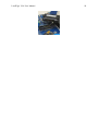
2.20 External Connector
The LandTiger LPC17XX development board has soldering connectors to provide access to
all processor I/O pins, powersupply and GND.
Figuur 23 External Connector (front)
LandTiger V2.0 User Manual
30
Figuur 24 External Connector (rear)
The pindescription is printed on the silkscreen (both front and rearside of PCB).
A detailed list of all pins and how they are used on the LandTiger is given in the Appendix.
LandTiger V2.0 User Manual
31
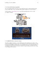
3 Color LCD, 3.2”, 320x240, 65K colours
LandTiger is compatible with several types of Color LCDs. There are currently two types of
3.2” displays available. Both displays are functionally identical, but have different LCD
panels and some differences in the electrical design. The displays are identified as HY32C
and HY32D.
Figuur 25 HY32C (left) and HY32D (right) seen from frontside
Notice that LCD HY32C has only one row of connectors and HY32D has two connectors
with identical pinout. Physical dimensions and mounting holes are also identical.
Figuur 26 HY32C (left) and HY32D (right) seen from rearside
Tabel 29 Characteristics of the LCDs
Characteristic
LCD Controller
Touch Screen Controller
LCD Type
LCD Interface
Touch Screen Interface
Backlight
Colors
Resolution
Backpanel illumination
Backlight voltage generator
Type
SSD1289 (Chip on Glass)
XPT2046
TFT
16-bit parallel
SPI
LED
65536
320 * 240 DOTS
LED
RT9293 (HY32C only)
LandTiger V2.0 User Manual
32
The main difference in the electrical design is that the HY32C has a different LCD panel
which also needs a voltage up converter to drive the backpanel LEDs. The converter device is
the RT9293.
Note1: The schematic of HY32C is not available.
Note2: The schematic of HY32D is available as part of the LandTiger documentation.
Tabel 30 Pinout Description of LCDs
Pin
Name
Description
Comment
1
5V
5V power supply
2
3
4
5
6
7
8
9
10
11
12
13
14
15
16
17
18
19
20
GND
D0
D1
D2
D3
D4
D5
D6
D7
D8
D9
D10
D11
D12
D13
D14
D15
/CS
RS
Ground
Data Lines
When powered from 5V supply:
Pin 1 & Pin 2 as power input,
Pin 33 & Pin 34 provide 3.3V output.
GND
D0-D15
21
22
23
24
25
26
27
/WR
/RD
/RESET
NC
BLVCC
BLGND
BLCNT
28
TP_IRQ
LCD chip select
Instruction / Data register
selection
Write
Read
Reset the controller chip
Do not connect
5 V or 3.3V
Ground
Backlight brightness
adjustment
Interrupt Touch screen
29
30
31
32
33
/TP_CS
TP_SCK
TP_SI
TP_SO
3.3V
Touch screen chip select
Touch screen SPI clock
Touch screen input date
Touch screen output data
3.3V power supply
Low active
RS = 1: Instruction Register
RS = 0: The Data Register
WR = 0, RD = 1
WR = 1, RD = 0
Low active
Do not connect
Backlight VCC
Backlight GND
Control of the backlight brightness
via PWM
Low level while the touch screen
detects pressing
Low active
Connects to SPI SCK
Connects to SPI MOSI
Connects to SPI MISO
When powered from 3.3V supply:
Pin 33 & Pin 34 as power input,
Pin 1 & Pin 2 keep NC.
LandTiger V2.0 User Manual
34
GND
Ground
Note1: The 5V-3V3 converter on the HY32C LCD board is interfering with LandTiger
mainboard 3V3 powersupply !!!!! The 0-Ohm resistor R58 should be removed from the
LandTiger mainboard.
33
LandTiger V2.0 User Manual
34
4 Downloading Application Software
4.1 In System Programming (ISP) using FlashMagic
Flashing a new program in the LandTiger LPC17xx may be done by entering the ISP
bootloader mode and downloading the new code through UART 0. A free PC software
application named FlashMagic may be used for this purpose (www.flashmagictool.com). All you
need is a serial cable (fully wired) between the PC and LandTiger COM0. Set JP6 and JP7 to
enable ISP mode via COM0. Select the LPC1768 device and the correct PC Com port in
FlashMagic, select the desired .hex file and press ‘Start’. Then press the Reset button on the
LandTiger to execute the new program.
Figuur 27 Flashmagic
Some compilers (e.g. mbed cloud compiler) produce a .bin file. FlashMagic needs a .hex file.
Convert the compiler .bin file with a modern bin2hex utility and use the /4 option for either 24
or 32 bit addressing range, not the standard 16 bit range. Example:
bin2hex /4 test.bin test.hex
An alternative bin2hex tool is part of the GNU toolsuite:
arm-none-eabi-objcopy -I binary -O ihex test.bin test.hex
Download the Bin2Hex from http://www.hex2bin.com/bin2hex, or if your running a 64-bit
system use this instead http://www.ht-lab.com/freeutils/bin2hex/bin2hex.zip)
Download the GNU tools from https://sourcery.mentor.com/sgpp/lite/arm/portal/release1802
Download the Keil bin2hex utility http://www.keil.com/download/docs/113.asp
LandTiger V2.0 User Manual
35
Download FlashMagic from www.flashmagictool.com
4.2 In System Programming (ISP) using the onboard JLink device
LandTiger LPC17XX development board has onboard support for JTAG debugging,
downloads and other features. The debugging port (CN4) provides access to the on-board
JLINK emulator (U3). JLINK is a JTAG emulator designed for ARM cores. It connects via
USB (CN4) to a PC running Microsoft Windows 2000, Windows XP, Windows 2003,
Windows Vista or Windows 7. The JTAG/SWD interface and JLINK emulator supports
KEIL, IAR and other mainstream development environments.
A PC application program such as JFlash will accept compiled .bin files and flash the target
processor. See www.segger.com for supported features.
Download JFlash software from www.segger.com. Install the software and run the JLink
commander application. J-Link commander (JLink.exe) is a command line based utility that
can be used for verifying proper functionality of J-Link as well as for simple analysis of the
target system. It supports some simple commands, such as memory dump, halt, step, go etc. to
verify the target connection.
Figuur 28 JLink Commader (Jlink.exe)
J-Flash is PC software running on Windows (Windows 2000 and later) systems, which
enables you to program the internal and external flash of your microcontroller via J-Link.
LandTiger V2.0 User Manual
36
Figuur 29 JFlash
In JFlash you first need to select the proper device (LPC1768) from the device database, then
select the .bin file and flash that into the target processor. Detailed instructions are given in
the JLink and JFlash manuals. See www.segger.com.
Note1: Many well known IDEs (eg Keil, IAR, CooCox and GNU GDB) support JLink
flashing and debugging without the need for the standalone JFlash application.
4.3 In System Programming (ISP) using external JLink devices
The JTAG/SWD interface (CN1) may also be connected to any external general purpose
JTAG/SWD debugging device. In this case the on-board JLINK emulator must be disabled by
inserting JP4.
External JLINK devices may be used for programming and debugging the ARM LPC1768 on
LandTiger. The JLLINK device is connected to a USB port on your PC and connects to the
targetboard using a JTAG connector (CN1).
Figuur 30 JLINK Setup
LandTiger V2.0 User Manual
37
Figuur 31 JLINK Flash and Debug device
A PC application program such as JFlash will accept compiled .bin files and flash the target
processor. See www.segger.com for a range of available devices and supported features.
Follow the explanations given above on using JLink Commander and JFlash.
Note1: Many well known IDEs (eg Keil, IAR, CooCox and GNU GDB) support JLink
flashing and debugging without the need for the standalone JFlash application.
Figuur 32 Converter for different JTAG and SWD connectors.
Note2: The standard connector on JLINK is the 20 pin JTAG connector. Converter boards
and cables may be needed sometimes to connect JLINK to the some of the other JTAG/SWD
plugs that are in use.
LandTiger V2.0 User Manual
38
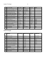
5 Portpin Usage on LandTiger vs mbed
Tabel 31 Port 0 description
IO
Pin
P0.0
P0.1
P0.2
P0.3
P0.4
P0.5
P0.6
P0.7
P0.8
P0.9
P0.10
P0.11
P0.12
P0.13
P0.14
P0.15
P0.16
P0.17
P0.18
P0.19
P0.20
P0.21
P0.22
P0.23
Description
Usage LandTiger
Comment LandTiger
Usage mbed
Comment mbed
P0.0/RD1/TXD3/SDA1
P0.1/TD1/RXD3/SCL1
P0.2/TXD0/AD0.7
P0.3/RXD0/AD0.6
P0.4/I2SRX_CLK/RD2/CAP2.0
P0.5/I2SRX_WS/TD2/CAP2.1
P0.6/I2SRX_SDA/SSEL1/MAT2.0
P0.7/I2STX_CLK/SCK1/MAT2.1
P0.8/I2STX_WS/MISO1/MAT2.2
P0.9/I2STX_SDA/MOSI1/MAT2.3
P0.10/TXD2/SDA2/MAT3.0
P0.11/RXD2/SCL2/MAT3.1
NA
NA
NA
P0.15/TXD1/SCK0/SCK
P0.16/RXD1/SSEL0/SSEL
P0.17/CTS1/MISO0/MISO
P0.18/DCD1/MOSI0/MOSI
P0.19/DSR1/SDA1
P0.20/DTR1/SCL1
P0.21/RI1/RD1
P0.22/RTS1/TD1
P0.23/AD0.0/I2SRX_CLK/CAP3.0
CAN1_RX
CAN1_TX
UART0_TX
UART0_RX
CAN2_RX
CAN2_TX
TP_CS
SCK1
MISO1
MOSI1
UART2_TX
UART2_RX
CAN1
CAN1
COM1
COM1
CAN2
CAN2
Touchscreen
Touchscreen
Touchscreen
Touchscreen
COM2
COM2
P9
P10
TXD0
RXD0
P30
P29
P8
P7
P6
P5
P28
P27
SDA1/TXD3
SCL1/RXD3
I/F MagicChip
I/F MagicChip
CAN_RD2
CAN_TD2
SSEL1
SCK1
MISO1
MOSI1
SDA2/TXD2
SCL2/RXD2
SCK
DF_CS
MISO
MOSI
LCD_EN
LCD_LE
LCD_DIR
LCD_CS
LCD_RS
SPI_Flash
SPI_Flash
SPI_Flash
SPI_Flash
LCD_8_16
LCD_8_16
LCD_8_16
LCD
LCD
P13
P14
P12
P11
NC
NC
NC
NC
P15
SCK0/TXD1
SSEL0/RXD1
MISO0
MOSI0
AD0.0
LandTiger V2.0 User Manual
P0.24
P0.25
P0.26
P0.27
P0.28
P0.29
P0.30
P0.31
P0.24/AD0.1/I2SRX_WS/CAP3.1
P0.25/AD0.2/I2SRX_SDA/TXD3
P0.26/AD0.3/AOUT/RXD3
P0.27/SDA0/USB_SDA
P0.28/SCL0/USB_SCL
P0.29/USB_D+
P0.30/USB_DNA
39
LCD_WR
LCD_RD
AOUT
SDA
SCL
USB_D+
USB_D-
LCD
LCD
Speaker
EEPROM
EEPROM
USB Host/Device
USB Host/Device
P16
P17
P18
NC
NC
P31
P32
AD0.1
AD0.2
AD0.3/AOUT
USB_D+
USB_D-
Tabel 32 Port 1 description
IO
Pin
P1.0
P1.1
P1.2
P1.3
P1.4
P1.5
P1.6
P1.7
P1.8
P1.9
P1.10
P1.11
P1.12
P1.13
P1.14
P1.15
P1.16
Description
Usage LandTiger Comment LandTiger
Usage mbed
Comment mbed
P1.0/ENET_TXD0
P1.1/ENET_TXD1
NA
NA
P1.4/ENET_TX_EN
NA
NA
NA
P1.8/ENET_CRS
P1.9/ENET_RXD0
P1.10/ENET_RXD1
NA
NA
NA
P1.14/ENET_RX_ER
P1.15/ENET_REF_CLK
P1.16/ENET_MDC
ENET_TXD0
ENET_TXD1
Ethernet
Ethernet
EN_TXD0
EN_TXD1
Ethernet
Ethernet
ENET_TX_EN
Ethernet
EN_TX_EN
Ethernet
ENET_CRS
ENET_RXD0
ENET_RXD1
Ethernet
Ethernet
Ethernet
EN_CRS
EN_RXD0
EN_RXD1
Ethernet
Ethernet
Ethernet
ENET_RX_ER
ENET_REF_CLK
ENET_MDC
Ethernet
Ethernet
Ethernet
EN_RX_ER
EN_RX_CK
EN_MDC
Ethernet
Ethernet
Ethernet
LandTiger V2.0 User Manual
P1.17
P1.18
P1.19
P1.20
P1.21
P1.22
P1.23
P1.24
P1.25
P1.26
P1.27
P1.28
P1.29
P1.30
P1.31
P1.17/ENET_MDIO
P1.18/USB_UP_LED/PWM1.1/CAP1.0
P1.19/MC0A/USB_PPWR/CAP1.1
P1.20/MCFB0/PWM1.2/SCK0
P1.21/MCABORT/PWM1.3/SSEL0
P1.22/MC0B/USB_PWRD/MAT1.0
P1.23/MCFB1/PWM1.4/MISO0
P1.24/MCFB2/PWM1.5/MOSI0
P1.25/MC1A/MAT1.1
P1.26/MC1B/PWM1.6/CAP0.0
P1.27/CLKOUT/USB_OVRCR/CAP0.1
P1.28/MC2A1.0/MAT0.0
P1.29/MC2B/PCAP1.1/MAT0.1
P1.30/VBUS/AD0.4
P1.31/SCK1/AD0.5
40
ENET_MDIO
USB_UP_LED
USB_PPWR
SCK0
SD_CS
USB_PWRD
MISO0
MOSI0
JOY_SEL
JOY_DOWN
JOY_LEFT
JOY_RIGHT
JOY_UP
VBUS
ADC_IN
Ethernet
USB Host/Device
USB Host/Device
SD_Card
SD_Card
USB Host/Device
SD_Card
SD_Card
Joystick
Joystick
Joystick
Joystick
Joystick
USB Host/Device
Potmeter
EN_MDIO
LED1
NC
LED2
LED3
NC
LED4
NC
LED_LNK
LED_SPD
EN_OS_EN
EN_RST
NC
P19
P20
Ethernet
Description
Usage LandTiger
Comment LandTiger
Usage mbed
Comment mbed
P2.0/PWM1.1/TXD1
P2.1/PWM1.2/RXD1
P2.2/PWM1.3/CTS1/TRACEDATA3
P2.3/PWM1.4/DCD1/TRACEDATA2
P2.4/PWM1.5/DSR1/TRACEDATA1
P2.5/PWM1.6/DTR1/TRACEDATA0
P2.6/PCAP1.0/RI1/TRACECLK
P2.7/RD2/RTS1
P2.8/TD2/TXD2
P2.9/USB_CONNECT/RXD2
P2.10/EINT0/NMI
DB00
DB01
DB02
DB03
DB04
DB05
DB06
DB07
485_DIR
USB_CONNECT
ISP
LCD_Bus
LCD_Bus
LCD_Bus
LCD_Bus
LCD_Bus
LCD_Bus
LCD_Bus
LCD_Bus
RS485
USB Host/Device
SW2,JP5/RTS,JP6
P26
P25
P24
P23
P22
P21
NC
NC
NC
USB_CON
TGT_SBL_ISP
PWM1.1/TXD1
PWM1.2/RXD1
PWM1.3
PWM1.4
PWM1.5
PWM1.6
Ethernet
Ethernet
Ethernet
Ethernet
AD0.4
AD0.5
Tabel 33 Port 2 description
IO
Pin
P2.0
P2.1
P2.2
P2.3
P2.4
P2.5
P2.6
P2.7
P2.8
P2.9
P2.10
LandTiger V2.0 User Manual
P2.11
P2.12
P2.13
P2.11/EINT1/I2STX_CLK
P2.12/EINT2/I2STX_WS
P2.13/EINT3/I2STX_SDA
41
KEY1
KEY2
TP_INT
SW4
SW3
Touchscreen
NC
NC
EINT3
JTAG_IRQ on mbed
Description
Usage LandTiger
Comment LandTiger
Usage mbed
Comment mbed
P3.25/MAT0.0/PWM1.2
P3.26/STCLK/MAT0.1/PWM1.3
SD_CD
SD_PWR
SD_Card
SD_Card
NC
NC
Description
Usage LandTiger
Comment LandTiger
Usage mbed
P4.28/RX_MCLK/MAT2.0/TXD3
P4.29/TX_MCLK/MAT2.1/RXD3
485_TX
485_RX
RS485
RS485
NC
NC
Tabel 34 Port 3 description
IO
Pin
P3.25
P3.26
Tabel 35 Port 4 description
IO
Pin
P4.28
P4.29
Comment mbed
LandTiger V2.0 User Manual
42
6 Software compatibility
6.1 Compatibility with Keil
See http://blog.tkjelectronics.dk/2011/09/review-poweravr-nxp-lpc1768-board/
The board has basically the same features and connections as the Keil MCB1700. This made
it possible to use the examples located in the Keil examples folder, for that specific board. It
just required some minor changes:
1. The LCD files should be replaced by the one from a WayEngineer example
(GLCD_SPI_LPC1700.c etc.)
2. The LED initializing and controlling part should be changed, as the LEDs are not
connected in the same way
3. If Analog inputs are used in the example this has to be fixed too, as in the Keil
examples, the used Analog inputs are on one of the same pins as the LCD data bus.
4. Unfortunately as all of the examples are using the Keil uVision compiler, you have to
download a use the evaluation period to test some of the examples (as they exceed the
Lite version limit).
It would have been good if they had made a couple of demonstrations for the free
GNU GCC compiler.
The WayEngineer website has many application examples (download the ZIP-file). Not all of
the demonstrations may compile with the latest Keil uVision, Most of the times this just
required the removal of the chip/system files, as these had to be loaded from the compiler
directory instead.
Regarding the Keil uVision everything was reported to works great. The On-board
programmer and debugger integrate nicely with the Keil environment – so it is very easy to
program and debug your application.
Some problems were noticed getting Keil to recognize and program the board, without giving
some kind of error. This was fixed by the following steps in each project:
1.
2.
3.
4.
5.
6.
7.
8.
Go to “Option for Target ‘…’” or press Alt+F7
Go to ‘Utilities’
Set programmer to “Cortex-M/R J-Link/J-Trace”
Click ‘Settings’ and then click ‘Add’
Find “LPC17xx IAP 512KB Flash”
Click ‘Add’ to confirm the selection
Finally tick ‘Program’, ‘Verify’ and “Reset and run”
And check “Erase full chip”
6.2 Compatibility with mbed
6.2.1 Hardware
LEDs
Pins
COM0
LandTiger V2.0 User Manual
43
PWM
Ethernet
mbed microcontroller boards have a built-in interface to provide functionality such as drag-ndrop download, reset, serial-over-usb, and access to the mbed local file system. These
functions provide means to control the interface using semihost calls it supports. The mbed
Ethernet library for example sets the MAC address by calling a weak function extern "C" void
mbed_mac_address(char * mac) to copy in a 6 Byte (12 character) MAC address. This
function performs a semihosting request to the mbed interface to get the serial number, which
contains a MAC address unique to every mbed device. If you are using the eth library on your
own board (i.e. not an mbed board like the LandTiger), you should implement your own
extern "C" void mbed_mac_address(char * mac) function to overwrite the existing one and
avoid a call to the interface (which doesn’t exist).
extern "C" void mbed_mac_address(char * mac) {
//MAC address may for example be cloned from scrapped modem box
mac[0]
mac[1]
mac[2]
mac[3]
mac[4]
mac[5]
};
=
=
=
=
=
=
0x00;
0x01;
0x02;
0x03;
0x04;
0x05;
Note1: the mbed has the ability to power down the PHY by disabling its oscillator (P1.27).
The mbed is also able to reset the PHY through P1.28. Both features are not supported on the
LandTiger. The PHY is always enabled and the reset occurs with the reset the LandTiger
board.
Probably best to avoid using P1.27 and P1.28 in your software to prevent interference with
the Ethernet library.
Note2: mbed uses the PHY LED_LINK and LED_SPEED outputs as digital inputs on P1.25
and P1.26. This allows mbed software to test the status and perhaps activate some other LED.
The LandTiger PHY has LEDs connected directly to its Link, Speed and Traffic outputs. The
processor pins P1.25 and P1.26 may be used for other purposes.
USB Device: Set jumpers JP9,JP11 to 1-2, Set jumper JP10 to 1-2 (Enable USB_CONNECT
P2_9), VBUS P1_30 not used, USB_UP_LED P1_18 not used.
USB Host: Set jumpers JP9,JP11 to 3-4, Enable USB_PPWR (P1_19 low), USB_PWRD
P1_19 not used,
The mbed interface functions that are define in ‘mbed_interface.h’ and which should be
overriden by user provide code are:
/* Function: mbed_interface_connected
* Determine whether the mbed interface is connected,
based on whether debug is enabled
*
LandTiger V2.0 User Manual
44
* Variables:
* returns - 1 if interface is connected, else 0
int mbed_interface_connected(void);
/* Function: mbed_interface_reset
* Instruct the mbed interface to reset, as if the
reset button had been pressed
*
* Variables:
* returns - 1 if successful, else 0 (e.g. interface not present)
*/
int mbed_interface_reset(void);
/* Function: mbed_interface_disconnect
* This will disconnect the debug aspect of the interface,
so semihosting will be disabled.
* The interface will still support the USB serial aspect
*
* Variables:
* returns - 0 if successful, else -1 (e.g. interface not present)
*/
int mbed_interface_disconnect(void);
/* Function: mbed_interface_powerdown
* This will disconnect the debug aspect of the interface, and if the
USB cable is not connected, also power down the interface. If the
USB cable is connected, the interface will remain powered up and
visible to the host
*
* Variables:
* returns - 0 if successful, else -1 (e.g. interface not present)
*/
int mbed_interface_powerdown(void);
/* Function: mbed_interface_uid
* This returns a string containing the 32-character UID of the mbed
interface
*
* This is a weak function that can be overwritten if required
*
* Variables:
* uid - A 33-byte array to write the null terminated 32-byte string
* returns - 0 if successful, else -1 (e.g. interface not present)
*/
int mbed_interface_uid(char *uid);
/* Function: mbed_mac_address
* This returns a unique 6-byte MAC address, based on
the interface UID
*
* If the interface is not present, it returns a default
fixed MAC address (00:02:F7:F0:00:00)
*
* This is a weak function that can be overwritten if you want to
provide your own mechanism to provide a MAC address.
LandTiger V2.0 User Manual
45
*
* Variables:
* mac - A 6-byte array to write the MAC address
*/
void mbed_mac_address(char *mac);
/* Function: mbed_die
* Cause the mbed to flash the BLOD LED sequence
*/
void mbed_die(void);
6.2.2 Downloading new application software
The mbed cloud compiler produces a .bin file. Convert the compiler .bin file with a modern
bin2hex utility to prepare the software for Flashmagic. JLINK will accept the .bin files
directly and flash the processor.
6.3 Compatibility with CooCox CoIDE for ARM
CooCox CoIDE for ARM is a free Eclipse based IDE for ARM Cores, using the GNU
Compiler (GCC). It supports ARM7/9 targets as well as Cortex-M0/M3/M4 targets. More
information about CoIDE and the installation process can be found here
http://www.coocox.org.
Please note that when using CoIDE for the first time, some additional setup is required to
enable GCC in CoIDE.
For more information, please refer to http://www.coocox.org/CoIDE/Compiler_Settings.html
In the following, a short step-by-step tutorial how to get up and running with CoIDE and JLink in general is given. For this tutorial, the sample project generator that is integrated into
CoIDE was used. Used components:
IDE
CoIDE V1.4.0
Emulator
J-Link
J-Link SW Version V4.40c
Evalboard
STM32F103ZE-EVAL (STM32F103ZG)
Additional SW
GCC Toolchain
Start CoIDE and click New Project button from the status bar.
Enter a Project Name and click Finish
Zie screendumps
Zie http://www.segger.com/cms/IDE_Integration_coocox.html
Copy ook de screenshots !!!
LandTiger V2.0 User Manual
46
7 JTAG Interface Description
The JTAG technology was defined by IEEE Std.-1149.1 standard and it exists for over a
decade. JTAG is used mostly for Connection testing and In System Programming (ISP).
The JTAG interface is 4/5-pin interface added to a chip, the interface is designed such that
multiple chips having a JTAG interface have their JTAG lines daisy-chained together, and a
test probe need only connect to a single “JTAG port” to have access to all chips on a circuit
board. The basic connector pins are:
Tabel 36 Basic JTAG Signals
Pin
Signal
Description
Comment
1
TDI
Test Data In
2
TDO
Test Data Out
3
TCK
Test Clock
4
TMS
Test Mode Select
5
TRST
Test Reset
optional.
7.1 JTAG standard connector for ISP and Debugging
Many modern programmable devices, such as FPGAs and CPLDs, are designed not only to be
JTAG compliant, but also support additional JTAG functionality to allow them to be
programmed after they have been attached to the circuit. Other devices, such as some flash
memories, can be programmed indirectly through their connection to devices in the JTAG
chain. The ability to use JTAG to program devices ‘in system’ avoids the need to buy
expensive programmers and socketed devices. There is also the advantage of being able to
easily update the image held on the device. The standard 20 pin 2.54mm (0.1”) JTAG
connector was defined by ARM. J-Link has a built-in 20-pin JTAG connector, which is
compatible with this standard.
Figuur 33 JTAG Standard 20 Pin Connector
Tabel 37 Standard JTAG interface 20 pin connector signals
Pin
1
Signal
VTref
Type
Input
Description
This is the target reference voltage.
LandTiger V2.0 User Manual
47
2
Vsupply
NC
3
nTRST
Output
5
TDI
Output
7
TMS
Output
9
TCK
Output
11
RTCK
Input
13
TDO
Input
15
RESET
I/O
It is used to check if the target has
power, to create the logic-level
reference for the input comparators
and to control the output logic levels
to the target. It is normally fed from
Vdd of the target board and must not
have a series resistor.
This pin is not connected in J-Link.
It is reserved for compatibility with
other equipment.
Connect to Vdd or leave open in target
system.
JTAG Reset.
Output from J-Link to the Reset signal
of the target JTAG port. Typically
connected to nTRST of the target
CPU. This pin is normally pulled
HIGH on the target to avoid unin
tentional resets when there is no
connection.
JTAG data input of target CPU.
It is recommended that this pin is
pulled to a defined state on the target
board. Typically connected to TDI of
target CPU.
JTAG mode set input of target CPU.
This pin should be pulled up on the
target. Typically connected to TMS of
target CPU.
JTAG clock signal to target CPU.
It is recommended that this pin is
pulled to a defined state of the target
board. Typically connected to TCK of
target CPU.
Return test clock signal from the
target.
Some targets must synchronize the
JTAG inputs to internal clocks. To
assist in meeting this requirement, you
can use a returned, and retimed, TCK
to dynamically control the TCK rate.
J-Link supports adaptive clocking,
which waits for TCK changes to be
echoed correctly before making
further changes. Connect to RTCK if
available, otherwise to GND.
JTAG data output from target CPU.
Typically connected to TDO of target
CPU.
Target CPU reset signal.
LandTiger V2.0 User Manual
48
17
DBGRQ
NC
19
5V-Target
supply
Output
Typically connected to the RESET pin
of the target CPU, which is typically
called "nRST", "nRESET" or
"RESET".
This pin is not connected in J-Link.
It is reserved for compatibility with
other equipment to be used as a debug
request signal to the target system.
Typically connected to DBGRQ if
available, otherwise left open.
This pin can be used to supply power
to the target hardware.
Note1: All pins marked NC are not connected inside J-Link. Any signal can be applied here;
J-Link will simply ignore such a signal.
Note2: Pins 4, 6, 8, 10, 12, 14, 16, 18, 20 are GND pins connected to GND in J-Link. They
should also be connected to GND in the target system.
Note3: Pin 2 is not connected inside J-Link. A lot of targets have pin 1 and pin 2 connected.
Some targets use pin 2 instead of pin 1 to supply VCC. These targets will not work with JLink, unless Pin 1 and Pin 2 are connected on the target's JTAG connector.
Note4: Pin 3 (TRST) should be connected to target CPUs TRST pin (sometimes called
NTRST). J-Link will also work if this pin is not connected, but you may experience some
limitations when debugging. TRST should be separate from the CPU Reset (pin 15)
Note5: Pin 11 (RTCK) should be connected to RTCK if available, otherwise to GND.
Note6: Pin 19 (5V-Target supply) of the connector can be used to supply power to the target
hardware. Supply voltage is 5V, max. current is 300mA. The output current is monitored and
protected againts overload and short-circuit.
There are also other JTAG connectors in use. This includes:
20 pin JTAG version with 2mm pin pitch and the same pinout as standard JTAG
14 pin JTAG version with 2.54mm pin pitch
10 pin JTAG version with 2.54mm (0.1”) pin pitch
10 pin JTAG version with 2.00mm pin pitch.
9 pin JTAG version with 1.27mm (0.05”) pin pitch
19 pin JTAG version with 1.27mm (0.05”) pin pitch
6 pin 2.54mm pin pitch socket - SWD Interface for Cortex Core
4 pin 2.54mm pin pitch socket - SWD Interface-Cortex Core
Tabel 38 JTAG interface 14 pin connector signals
Pin
1
Signal
VTref
Type
Input
Description
This is the target reference voltage.
It is used to check if the target has
LandTiger V2.0 User Manual
49
power, to create the logic-level
reference for the input comparators
and to control the output logic levels
to the target. It is normally fed from
Vdd of the target board and must not
have a series resistor.
2
3
GND
nTRST
I/O
Target CPU reset signal.
Typically connected to the RESET pin
of the target CPU, which is typically
called "nRST", "nRESET" or
"RESET".
4
5
GND
TDI
Output
JTAG data input of target CPU.
It is recommended that this pin is
pulled to a defined state on the target
board. Typically connected to TDI of
target CPU.
6
7
GND
TMS
Output
JTAG mode set input of target CPU.
This pin should be pulled up on the
target. Typically connected to TMS of
target CPU.
8
9
GND
TCK
Output
JTAG clock signal to target CPU.
It is recommended that this pin is
pulled to a defined state of the target
board. Typically connected to TCK of
target CPU.
10
11
GND
TDO
Input
JTAG data output from target CPU.
Typically connected to TDO of target
CPU.
12
13
nSRST
Vsupply
NC
This pin is not connected in J-Link.
It is reserved for compatibility with
other equipment.
Connect to Vdd or leave open in target
system.
14
GND
Tabel 39 JTAG interface 10 pin connector signals
Pin
1
Signal
VTref
Type
Input
Description
This is the target reference voltage.
It is used to check if the target has
power, to create the logic-level
reference for the input comparators
and to control the output logic levels
to the target. It is normally fed from
LandTiger V2.0 User Manual
50
2
Vsupply
NC
3
RESET
I/O
4
RESET
I/O
5
TDI
Output
6
NC/TDO
NC/Input
7
TMS
Output
8
9
GND
TCK
Output
10
GND
Vdd of the target board and must not
have a series resistor.
This pin is not connected in J-Link.
It is reserved for compatibility with
other equipment.
Connect to Vdd or leave open in target
system.
Target CPU reset signal.
Typically connected to the RESET pin
of the target CPU, which is typically
called "nRST", "nRESET" or
"RESET".
Target CPU reset signal.
Typically connected to the RESET pin
of the target CPU, which is typically
called "nRST", "nRESET" or
"RESET".
JTAG data input of target CPU.
It is recommended that this pin is
pulled to a defined state on the target
board. Typically connected to TDI of
target CPU.
JTAG data output from target CPU.
Typically connected to TDO of target
CPU.
JTAG mode set input of target CPU.
This pin should be pulled up on the
target. Typically connected to TMS of
target CPU.
JTAG clock signal to target CPU.
It is recommended that this pin is
pulled to a defined state of the target
board. Typically connected to TCK of
target CPU.
7.2 SWD and SWO/SWV (also called SWV) compatibility
The J-Link and J-Trace support ARMs Serial Wire Debug (SWD). The SWD replaces the
standard JTAG port with a clock (SWDCLK) and a single bi-directional data pin (SWDIO),
providing all the normal JTAG debug and test functionality. SWDIO and SWCLK are
overlaid on the TMS and TCK pins. In order to communicate with a SWD device, J-Link
sends out data on SWDIO, synchronous to the SWCLK. With every rising edge of SWCLK,
one bit of data is trans- mitted or received on the SWDIO. The data read from SWDIO can
than be retrieved from the input buffer.
LandTiger V2.0 User Manual
51
Tabel 40 SWD pinout on 20 pin connector
Pin
1
Signal
VTref
Type
Input
2
Vsupply
NC
3
Not used
NC
5
Not used
NC
7
9
SWDIO
SWCLK
I/O
Output
11
Not used
NC
13
SWO
Output
15
RESET
I/O
17
19
Not used
5V-Supply
NC
Output
Description
This is the target reference voltage. It
is used to check if the target has
power, to create the logic-level
reference for the input comparators
and to control the output logic levels
to the target. It is normally fed from
Vdd of the target board and must not
have a series resistor.
This pin is not connected in J-Link. It
is reserved for compatibility with
other equipment. Connect to Vdd or
leave open in target system.
This pin is not used by J-Link. If the
device may also be accessed via
JTAG, this pin may be connected to
nTRST, otherwise leave open.
This pin is not used by J-Link. If the
device may also be accessed via
JTAG, this pin may be connected to
TDI, otherwise leave open.
Single bi-directional data pin.
Clock signal to target CPU. It is
recommended that this pin is pulled to
a defined state of the target board.
Typically connected to TCK of target
CPU.
This pin is not used by J-Link. This
pin is not used by J-Link when
operating in SWD mode. If the device
may also be accessed via JTAG, this
pin may be connected to RTCK,
otherwise leave open.
Serial Wire Output trace port.
(Optional, not required for SWD
communication.)
Target CPU reset signal. Typically
connected to the RESET pin of the
target CPU, which is typically called
"nRST", "nRESET" or "RESET".
This pin is not connected in J-Link.
This pin is used to supply power to
some eval boards. Not all JLinks
supply power on this pin, only the KS
(Kickstart) versions. Typically left
open on target hardware.
LandTiger V2.0 User Manual
52
Note1: Pins 4, 6, 8, 10, 12, 14, 16, 18, 20 are GND pins connected to GND in J-Link. They
should also be connected to GND in the target system.
7.3.1 Serial Wire Output (SWO) compatibility
J-Link can be used with devices that support Serial Wire Output (SWO). Serial Wire Output
(SWO) support means support for a single pin output signal from the core. It is currently
tested with Cortex-M3 only.
The supported SWO speeds depend on the connected emulator. They can be retrieved from
the emulator. Currently, the following are supported:
Emulator
J-Link V6
J-Link V7
Speed, formula
6MHz/n, n >= 12
6MHz/n, n >= 1
Resulting max. speed
500kHz
6MHz
7.3.2 Serial Wire Viewer (SWV) compatibility
The Instrumentation Trace Macrocell (ITM) and Serial Wire Output (SWO) can be used to
form a Serial Wire Viewer (SWV). The Serial Wire Viewer provides a low cost method of
obtaining information from inside the MCU. The SWO can output trace data in two output
formats, but only one output mechanism is valid at any one time. The two defined encodings
are UART and Manchester. The current J-Link implementation supports only UART
encoding. Serial Wire Viewer uses the SWO pin to transmit different packets for different
types of information. The three sources in the Cortex-M3 core which can output information
via this pin are:
Instrumentation Trace Macrocell (ITM) for application-driven trace source that
supports printf-style debugging. It supports 32 different channels, which allow it to be
used for other purposes such as real-time kernel information as well.
Data Watchpoint and Trace (DWT) for real-time variable monitoring and PCsampling, which can in turn be used to periodically output the PC or various CPUinternal counters, which can be used to obtain profiling information from the target.
Timestamping. Timestamps are emitted relative to packets.
7.3.3 Cortex 10 Pin Debug compatibility
The Cortex Debug Connector provides support for Serial Wire and JTAG interface modes in a
very small, low cost 10-pin (0.05") connector. This new style connector provides access to all
SWD, SWV, and JTAG signals available on a Cortex-Mx device.
A 10-pin header (Samtec FTSH-105-01) is specified with dimensions: 0.25" x 0.188"
(6.35mm x 4.78mm).
LandTiger V2.0 User Manual
53
7.3.4 Cortex 20 Pin Debug compatibility
The Cortex Debug+ETM Connector is a new small 20-pin (0.05") connector that provides
access to SWD, SWV, JTAG, and ETM (4-bit) signals available on a Cortex-M3 device.
A 20-pin header (Samtec FTSH-110-01) is specified with dimensions: 0.50" x 0.188"
(12.70mm x 4.78mm).
Figuur 34 Standard and smaller new connectors
7.3.5 ARM ETM 'Mictor' Connector (38-pin)
The Mictor (Matched Impedance ConnecTOR) has been the standard way to connect a trace
probe to an ARM target. It supports up to 32-bit ETM trace and is really intended for use with
very high-speed ARM processors such as Cortex-R4 and Cortex-A9. As Cortex-M3 ETM
only supports 4-bit trace, the best connector solution to support debug and ETM is the 20-pin
Cortex Debug+ETM connector.
LandTiger V2.0 User Manual
54
LandTiger V2.0 User Manual
8 References
PowerMCU: www.PowerMCU.com
LandTiger Schematic: LandTiger V2.0 Schematic.pdf
HY32D Schematic: HY32D_SCH.pdf
HY32C Schematic http://propix.com.pl/pl/p/LCD-3.2-TFT-SSD1289-HY-32C/194
ARM: www.arm.com
NXP: www.nxp.com
LPC1768 Datasheets and Documentation: www.nxp.com
Keil Compilers and IDE: www.keil.com
JLINK: www.segger.com.
GNU tools: https://sourcery.mentor.com/sgpp/lite/arm/portal/release1802
Flashmagic: http://www.flashmagictool.com/
Mbed: www.mbed.org
Bin2Hex: http://www.hex2bin.com/bin2hex
(or if your running a 64-bit system use this instead
http://www.ht-lab.com/freeutils/bin2hex/bin2hex.zip )
CooCox IDE: http://www.coocox.org
55