1
EEL 4514L
COMMUNICATION LABORATORY
Laboratory Manual
G.K. Heitman
Electrical and Computer Engineering
University of Florida
Spring 2007
TABLE OF CONTENTS
Laboratory
–
1
2
3
4
5
6
7
8
9
10
Appendix
A
B
C
D
E
Title
Introduction To the Communication Laboratory
The Digital Storage Oscilloscope, the Function Generator, and Measurements
The Spectrum Analyzer and Measurements
Frequency Response of Systems and Distortion
Sinusoidal Oscillators
Amplitude Modulated Signals and Envelope Detection
AM Modulators
The Phase-Locked Loop and Frequency Modulation and Demodulation
More Frequency Modulation/Demodulation
Sampling and Pulse Amplitude Modulation
ISI and Eye Diagrams
Title
Basics of the Digital Storage Oscilloscope
Basics of the Spectrum Analyzer
Some Background on Oscillators
Amplitude Modulators, Mixers, and Frequency Conversion
The Phase-Locked Loop
INTRODUCTION TO THE
COMMUNICATION LABORATORY
1
Purpose of the Laboratory Course
The goals of the communication laboratory are:
1. to allow you to perform experiments that demonstrate the theory of
signals and communication systems that will be discussed in the lecture
course,
2. to introduce you to some of the electronic components that make up
communication systems (which are not discussed in the lecture course
because of time limitations), and
3. to familiarize you with proper laboratory procedure; this includes precise record-keeping, logical troubleshooting, safety, and learning the
capabilities as well as the limitations of your measurement equipment.
2
General Laboratory Procedure
The most important rule to follow in any laboratory is: think before
you do anything. If you follow this one rule you will avoid injury to
yourself, damage to the system you are testing, damage to your measurement
equipment, and you will not waste time going down dead-end streets.
Safety In general you will not be using voltage levels high enough to cause
injury; nevertheless, you should always pay attention to what you are
doing.
Circuit Damage Your voltage levels can cause damage to the circuit under test if you are not careful. Make sure that your circuit diagram
is correct, and be careful to build the circuit correctly on the protoboard. If you need to make changes to the circuit, disconnect the
power supply and the input signal.
1
Introduction
2
Equipment Each lab station has the following permanent equipment that
you will use for most labs:
Spectrum Analyzer Agilent E4411B Spectrum Analyzer
Oscilloscope Agilent 54622D Mixed Signal Oscilloscope
Signal Generator Agilent 33120A Arbitrary Function Generator (2
per station)
Multimeter Agilent 34401A Digital Multimeter
Power Supply Agilent E3631A Triple-Output DC Power Supply
Before you use any measurement equipment, know the maximum input signal level it can withstand, and make sure that the signal you are
trying to measure does not exceed it. (All good measurement equipment has overload protection, but it is still possible to do damage; do
not rely on the equipment to protect you from your own mistakes.)
In general, the signals in this laboratory course will not cause damage
to the oscilloscope. (You can find the maximum voltage ratings on
the front panel, next to the connectors.) The same is not true of the
spectrum analyzer; you must be very careful what signal you apply to
it. (Again, the maximum signal that can be applied is printed on the
front panel.)
A big part of this laboratory course is learning how to use measurement
equipment; you learn how to make good measurements by actually
using the instruments to measure things. The lab experiments in this
manual will not be a step-by-step procedural list—you will not be
told which button to push, which menu to bring up in order to make
the instrument do something. Rather, you will be told things such
as “display the output signal on the oscilloscope and determine its
frequency components”. You will have to learn how to accomplish
this. To help you, the complete User’s Guide for each instrument is on
the PC at each station. On the PC desktop you will find a shortcut to
a folder called Equipment Manuals; all of the User’s Guide are there
in PDF format. Double-click the one you want to open in the Acrobat
Reader.
Troubleshooting Things will not always go as expected; that is the nature
of the learning process. When you are testing a circuit, especially one
that you have built, if the output signal is not what you expect do
not go in and randomly replace chips and other components. The
Introduction
3
key is to be logical and systematic; don’t just try things at random
hoping to get lucky. First, look for obvious errors that are easy to fix.
Is your measuring device correctly set and connected? Is the power
supply set for the correct voltage and is it connected correctly? Is the
signal generator correctly set and connected? Next, check for obvious
misconnections or broken connections, at least in simple circuits. If
the problem is not one of these trivial ones, then you need to get to
work. As you work through your circuit, use your notebook to record
tests that you make and changes that you make as you go along; don’t
rely on your memory for what you have tried. Identify some test points
in the circuit at which you know what the signal should be, and work
your way backwards from the output through the test points until you
find a good signal. Now you have a section of the circuit to focus
your efforts on. (Here is where a little thought about laying out your
board before connecting it up will pay off; if your board looks like a
bird’s nest, it is going to be very hard to troubleshoot, but if it is well
organized and if the wires are short, it is going to make your job a lot
easier.) Final remark: if you do discover a bad component or wire, do
not just throw it back in the box.
Neatness When you have finished for the day, return all components to
their proper storage bins, return all test leads and probes to their
storage racks or pouches, return all equipment to its correct location,
and clean up the lab station.
Computers On occasion you will find that measurements made in lab do
not check with your prelab calculations or simulations; the PC’s at
each station have Mathcad and (Microsim) PSpice on them so that you
can check your prelabs. The PC’s are not conncected to the campus
network. The PC’s are also used to give you access to a printer so you
can print out oscilloscope and spectrum analyzer displays. Do not
install other software on the computers, change the system settings
(such as the display), change the desktop, install your own wallpaper
or screen saver, etc. You may temporarily save your own files on the
hard disk; you will find a shortcut to the My Documents directory on
the desktop. You may create your own folders under My Documents to
store files in. Do not, however, expect those files to be there next time
you use the computer; the computers will be cleaned up periodically
to provide disk space. Always copy any files you need to save
onto your own floppy before you leave the lab.
Introduction
4
Final note: when you start the PC, do not logon. When the logon
screen comes up, just hit the Esc key.
3
Record-Keeping
You will be working in groups of 2 at the lab stations, but each student
will maintain a standard laboratory notebook into which all calculations,
measurements, prelabs, answers to questions, etc. are entered. Your notebook will be checked each week for adequate progress during the course.
The laboratory notebook is a record of your lab activity, not a series of formal lab reports. You should try to keep the notebook neat and organized,
but perfection is not expected. Occasionally you will make an entry that
is simply wrong; do not erase or tear out the page, but merely cross out
the entry. (In industry you will be required to keep a patent notebook in
ink—no erasures at all are allowed. We shall be more relaxed—small errors
may be erased, but do not waste time erasing a half-page, just cross it out.)
Most of the lab experiments have prelabs, involving PSpice, Mathcad,
or Matlab, as well as derivations or calculations to do by hand. All of the
prelabs must be entered into your notebook; any printouts they include
should be securely pasted or taped into your notebook. The same is true
of any printouts you make of the oscilloscope and spectrum analyzer displays. (You may also paste the experiments from this lab manual into your
notebook, but that is not required, nor is it recommended.)
Each student is expected to participate in the lab and to maintain a
notebook; remember, your notebook will be checked each week, and there
will be a final practical exam—if you have not kept up with the labs, you
will not do well on the final.
4
Prelabs
Most of the experiments have prelabs. You will be expected to have the
prelab completed before the lab period— you will not be permitted
to do the in-lab part of the experiment without a complete prelab.
You are encouraged to use any computer tool that you consider appropriate
to help you complete the prelab. The tools available in the ECE computer
lab (NEB 288) that you will find most useful are PSpice, Mathcad, and
Matlab. The computers at each station in the lab also have Microsim PSpice
and Mathcad installed. If you use one of these tools to produce a circuit
diagram, a graph, or a table, then you must secure that page in your lab
Introduction
5
notebook; your graphs must have titles and axis labels, and if you have more
than one trace on a graph the traces must be labeled. Circuit diagrams
drawn by hand should be entered directly into your notebook, as neatly
as possible, with all components clearly labeled. If you choose to draw a
graph by hand, then you must do it on appropriate graph paper, using a
straightedge to draw axes. You are an engineer—you are expected to
present data and calculations clearly and precisely.
LABORATORY 1
THE DIGITAL STORAGE
OSCILLOSCOPE, THE FUNCTION
GENERATOR, AND MEASUREMENTS
OBJECTIVES
1. To become familiar with the features and basic operation of the Agilent
54622D oscilloscope and the Agilent 33120A function generator.
2. To investigate signals in the time and frequency domains.
PRELAB
1. Review Appendix A of this manual; it contains basic information on
how a digital storage oscilloscope works in general, with some specific
information on the Agilent 54622D DSO.
2. Calculate and plot1 the exponential Fourier series coefficients for a
sinusoidal voltage of amplitude A, frequency f0 , phase angle θ, and dc
value (i.e. average value) of K.
3. Calculate and plot the exponential Fourier series coefficients of a square
wave of amplitude A, frequency f0 , duty cycle 50%, and dc value K.
(Use an odd square wave.)
4. Calculate and plot the transfer function of an RC lowpass filter for a
given time constant τ = RC. Indicate the 3-dB bandwidth on your
plot.
5. For your RC lowpass filter, calculate and plot the output spectrum and
the output time signal for a sinusoidal input and for a square input.
1
Be sure to heed the advice in the Introduction about plots and graphs.
1
Lab 1
2
6. Design an RC lowpass filter having time constant τ = 10 µs. What is
the 3-dB break frequency?
IN LAB
1. On the desktop of the computer at your station you will find a shortcut to a folder called “Equipment Manuals”. This folder contains, in
PDF format, the complete User’s Guides to the oscilloscope, function
generator, multimeter, DC power supply, and spectrum analyzer. (In
addition there is a Quick Reference Guide and a Front Panel Guide for
the function generator.) Locate these manuals and be ready to open
them as needed. (Double-click on the name to open the manual with
the Acrobat reader.)
2. Use the function generator to produce a sine wave of frequency 2.5 kHz
and peak-to-peak amplitude 200 mV, with zero dc offset. Use a coaxial cable with BNC connectors on the ends to connect the output of
the signal generator to one of the analog inputs on the oscilloscope.
Display the sine wave on the oscilloscope and measure the frequency
and amplitude in two ways: (1) By counting divisions on the screen
to determine the amplitude and the period. (Use the cursors to help
you make the measurements—see the oscilloscope manual for information on using cursors.) (2) By having the oscilloscope automatically
make the measurements. (Manual again.) Always pay attention to
the information on the status line (above the waveform display) and
on the measurement line (below the waveform display); see p.2-11 in
the manual.
Is there a discrepancy between your measured amplitude and the amplitude you entered into the function generator? Explain. (Hint:
check the output impedance of the function generator and the input
impedance of the oscilloscope. Take a look at the Function Generator
Front Panel guide in the Equipment Manuals folder.)
3. Take a few minutes to become familiar with the front panel controls
of the two devices.
On the function generator, learn how to select waveshapes, amplitudes and frequencies using the keypad and the control knob. What
is the maximum frequency and maximum amplitude sine wave that
the function generator can produce? What is the minimum frequency
Lab 1
3
and minimum amplitude that it can produce? (Make sure that the
maximum amplitude does not exceed the maximum input rating of
the oscilloscope.)
On the oscilloscope, learn how to select channels to display, and how
to get a good display without using the Autoscale button. (Autoscale
does not do anything you cannot do with the controls, and there is no
guarantee that it will give the display settings you need.) Spend some
minutes investigating the following features (you do not need to record
this in your notebook, unless you want to for your own reference):
(a) What does the Delayed Sweep feature do?
(b) What are the three triggering modes that this oscilloscope provides?
(c) What are the trigger coupling modes?
(d) The signal must also be coupled to the input of the oscilloscope—
what is the difference bewtween AC and DC input coupling?
(e) What are the different acquisition modes that this oscilloscope has?
(f) What do the RUN/STOP and SINGLE buttons do?
You must learn to become familiar with these features and to pay
attention to them. Every time you make a measurement with an oscilloscope, you must know how the input is coupled, how the waveform
is acquired, how the oscilloscope is triggered, and the sampling rate
being used. If you do not pay attention, you could end up displaying
on the screen a waveform that in no way represents the signal you are
trying to measure.
4. Reset the function generator to produce the 2.5 kHz sine wave from
Step 2.
(a) Find out how to save the trace and the oscilloscope settings to one
of the three internal memories, and do so. Disconnect the signal generator. Recall the saved trace from the internal memory location and
display it. (This is useful when you want to compare a measurement
to a known good measurement that has been stored.)
(b) Clear the recalled trace from the screen. Reconnect the signal
generator and redisplay the “live” sine wave. Now save the trace and
oscilloscope settings to a floppy disk, and recall the saved trace from
the floppy. Saving the trace and settings on a disk allows you to
transfer them to another oscilloscope (the same or compatible model,
Lab 1
4
of course). Note that you can also save the screen in other formats,
such as Windows bitmap (*.bmp).
5. Display the amplitude spectrum of the sine wave on the oscilloscope.
Remember that the oscilloscope does this by calculating the FFT of
the samples of the signal it has acquired. You will need to adjust the
sampling rate (through the horizontal sweep control), the center frequency, and the frequency span to get a good display. Compare with
your prelab calculations. Why is the spectrum as shown by the oscilloscope not a pure line spectrum as in your prelab plot? In particular,
address these two points:
(a) Why is there more than one line? (Hint: measure the amplitude
level, in dB, of the higher order lines relative to the fundamental line.
How much power is contained in the higher order lines? Is the signal
generator producing a perfect sine wave?)
(b) Why are the lines not truly lines? That is, they have non-zero
width. (Hint: In order to calculate the FFT, the oscilloscope can only
use a finite number of samples; i.e., the signal is windowed to have
a finite time duration. What is the Fourier transform of a sinusoidal
pulse?)
6. Save the display of the spectrum on a floppy as a bitmap, print it out
and include it in your notebook.
7. Use the HP function generator to produce a 10 kHz square wave with
peak-to-peak value 200 mV, 50% duty cycle, and zero dc offset. Display it on the oscilloscope, and display its FFT. Include a printout
of the square wave and its FFT in your lab notebook. Compare its
amplitude spectrum, out to the first five peaks, with your prelab calculations.
8. Build the RC lowpass filter having time constant τ = 10 µs from your
prelab. Use the square wave from Step 7 as the input to the RC
filter. Display the output signal and its FFT; insert a printout in your
notebook. Compare the output to your prelab calculations.
9. Measure the time constant τ of the RC circuit and compare with the
designed value. Hint: use a square wave test input, and measure the
rise time of the output. Calculate τ from the measured rise time. The
Delayed Sweep feature of the oscilloscope will be helpful here—you
Lab 1
5
can use it to “zoom-in” on the rising edge of the output waveform and
get a more accurate measurement of the rise time.
LABORATORY 2
THE SPECTRUM ANALYZER AND
MEASUREMENTS
OBJECTIVES
1. To become familiar with the features and basic operation of the Agilent
E4411B spectrum analyzer.
2. To investigate signals in the frequency domain.
PRELAB
1. Review Appendix B on the basic operation of the spectrum analyzer.
2. You will need your Prelab calculations from Laboratory 1: Fourier
series for sine and square waves, transfer function for an RC lowpass
filter, and the outputs of an RC filter for sine and square inputs.
3. Design an RC lowpass filter with a 3 dB break frequency of 120 kHz
(or as near as you can get with the available resistors and capacitors).
4. Review Section 2-1 in [Couch] about normalized signal power, signal
power into a load, and signal power in units of dBm.
IN LAB
1. As discussed in Appendix B, you need to let the spectrum analyzer
warm up for 5 minutes, and go through its internal alignment procedure.
2. Record the answers to the following questions in your lab notebook:
1
Lab 2
2
• What is the frequency range that this spectrum analyzer will
measure?
• What is the maximum DC level that can be applied to the RF
input?
• What is the input impedance of the RF input?
• What is the maximum signal power, in dBm and in Watts, that
can be applied to the RF input?
Before you connect any signal to the RF input, be sure that its amplitude or power does not exceed the maximum rated input. If you are
unsure, measure the signal with the oscilloscope.
3. Given your answers to the questions in Item 2, calculate
• the maximum amplitude sine wave (with zero DC offset) that can
be applied to the RF input,
• the maximum amplitude square wave (with zero DC offset) having 50% duty cycle that can be applied to the RF input.
(When doing these calculations, don’t forget what the input impedance
of the analyzer is.)
• What is the center frequency and the frequency span on powerup?
• What is the resolution bandwidth on power-up?
• What is the reference level and the amplitude scale in dB/division?
• What is the attenuation? What is the purpose of the internal
attenuator?
4. With no signal applied and with the analyzer in its default configuration (if you changed any of the settings you can get back to the
default state by pressing the PRESET button), you will see the display
of the noise floor. This noise is approximately white noise, meaning its power spectral density (which is what you are looking at on
the screen) is approximately constant for all frequencies. Measure the
power level in dBm and in W of this noise.
5. Use the 33120A function generator to produce a 1 MHz sine wave of
amplitude 200 mVp-p . (Remember that you can set the function generator output impedance to high or to 50 Ω—make sure you have it set
Lab 2
3
appropriately.) Get a good display of the spectrum on the analyzer.
Measure the input power in dBm (don’t forget that you are not measuring normalized power) of the lines and compare with theory. Make
sure that you look for lines other than the ones you expect to see, and
that you record their frequencies and amplitudes.
6. Change the vertical unit from dBm to mV and repeat item 5.
7. Adjust the resolution bandwidth (RBW) up and down and observe
the effect on the displayed spectrum. Explain the appearance of the
spectrum as you change the RBW, especially when you set the RBW
to 1 MHz and 3 MHz
8. Use the Sweep control to obtain a single sweep and a continuous sweep
(the default). What is the purpose of single sweep?
9. With the sine wave spectrum displayed, become familiar with using
the FREQUENCY, SPAN, AMPLITUDE, and Res BW controls. Become familiar with the Marker controls for frequency and amplitude
measurements, including the difference markers and the Peak Search
control. What is the function of the Signal Track control?
10. Investigate the effect of the Video BW (video filter bandwidth) button
on the display of the calibration signal. The video filter is a postdetection filter used to reduce noise in the displayed spectrum to its
average value, making low-level signals easier to detect. Note: you
should use the reduced VF bandwidth with care—it will reduce the
indicated amplitudes of wideband signals, such as video modulation
and short duration pulses. When you have finished this item, put the
spectrum analyzer back in its default configuration with the PRESET
button.
11. Use the function generator to produce a 100 kHz square wave of amplitude 200 mVp-p , with 50% duty cycle and zero dc offset. Get a good
display of the fundamental and the first several (at least out to the
5th ) harmonics. Which harmonics do you expect to see, and what
do you observe? Explain. Measure how far below the fundamental
the harmonics are, in dBm. Comment on the difference in amplitude
between the even and odd harmonics. Compare with the theoretical
values.
12. Get the display of the square wave spectrum the way you want it; print
it and include it in your notebook. Explore the File control menus.
Lab 2
4
Note that, as with the oscilloscope, you can save the screen or the
instrument configuration internally or on a floppy, you can organize
the file structure (create directories, rename files), etc.
13. Build an RC lowpass filter having 3 dB bandwidth 120 kHz. Use the
square wave from Item 11 as the input to the RC filter, and observe
the spectrum of the output on the analyzer. Measure the fundamental
and at least out to the 5th harmonic of the output. Compare with
theory.
Also print out the filter output and include in your notebook.
Note: depending on how you connect the function generator to your
circuit, and how you connect the output of the circuit to the RF input
of the analyzer (you will probably use the cables that have a BNC
connector on one end and alligator clips on the other), your amplitude
measurements may not be accurate due to impedance mis-matches.
But your relative amplitude measurements will be accurate—i.e., the
amplitude values of the lines in dBm may not agree with theory, but
the differences between the lines in dB should.
Remarks : In this lab we of course have not used the spectrum analyzer
to its full advantage—we did nothing here that could not have been done
with the FFT feature of the oscilloscope. The purpose of this lab was simply
to introduce you to the spectrum analyzer and its basic operation. In future
you will be expected to be able to set the analyzer controls to get a good
display of the spectrum of any signal, and to be able to read the frequencies
and amplitudes of the spectral components from the display and convert the
amplitudes into voltage levels or normalized powers.
References
[Couch] Leon W. Couch, II, Digital and Analog Communication Systems, 6th ed., Prentice-Hall (2001)
LABORATORY 3
FREQUENCY RESPONSE OF
SYSTEMS AND DISTORTION
OBJECTIVE
To measure the frequency response of a linear filter and to investigate linear
and nonlinear distortion.
PRELAB
1. Read the following: in [Couch], Section 2-6, subsection on distortionless transmission, and Section 4-9 on nonlinear distortion; or in
[Carlson], Section 3.2.
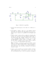
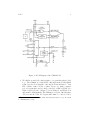
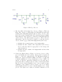
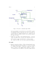
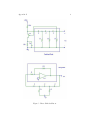
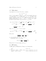
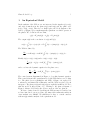
2. A popular type of Butterworth second-order lowpass filter is the SallenKey circuit shown in Figure 1.1 Assuming an ideal op-amp, show that
the transfer function of this linear system is
H(s) =
1
Vout (s)
=
.
Vin (s)
R1 R2 C1 C2 s2 + (R1 + R2 )C2 s + 1
(1)
A useful assumption for design is R1 = R2 = R and C1 = C2 = C;
under this assumption obtain an expression, in terms of R and C,
for the 6 dB break frequency. (The 6 dB frequency is simply more
convenient to deal with than the usual 3 dB frequency.)
1
You will learn about Butterworth filters in Electronics 2. The Sallen-Key circuit
was invented around 1955 (by Sallen and Key, surprisingly), and it is popular because it
requires only one op-amp, hence it is inexpensive and does not consume much power. Its
Q factor is, however, more sensitive to component tolerances than other configurations,
especially for large Q. But in lowpass filters, Q is not large and the sensitivity problem is
not a concern. See Sec. 11.8 in [Sedra/Smith]
1
Lab 3
2
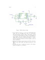
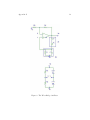
Figure 1: Sallen-Key Lowpass Filter
3. Find the 6 dB break frequency for the values R = 8.2 kΩ and C =
0.01 µF.
4. Using Mathcad or Matlab, obtain a plot of the amplitude gain and
phase shift of the Sallen-Key filter using Equation (1). It is best to
make Bode plots—frequency on a logarithmic scale and amplitude gain
in dB.
5. Using the R and C values from Item 3, simulate the Sallen-Key filter
in PSpice and obtain a Bode plot of the amplitude gain (in dB) over
the frequency range 1 Hz to 100 kHz. Determine the slope, in dB per
decade, of the high frequency asymptote. Be sure to choose Vcc and
the input ampltitude so that the op-amp does not saturate—i.e., make
sure the circuit is operating as a linear system. In lab you will use
Vcc = 5 V, so choose the input amplitude appropriately.
Hint: Recall that to get a frequency response plot in PSpice, use the
VAC source for the input and in the simulation setup set the paramters
under AC Sweep. It is convenient to use a voltage dB marker or
phase marker at the ouput, depending on which part of the frequency
response you want.
6. Compare your theoretical Bode plot from Item 4 with the circuit simulation result from Item 5. They should of course be close. Your
theoretical anlaysis was based on an ideal op-amp and your simulation
Lab 3
3
uses the Spice model of the op-amp, so supposedly the simulation is
more accurate to some degree. (This should always be your procedure.
You do some analysis and design based on a simplified mathematical
model. Now you have some idea of how the system should behave.
Next you verify your analysis by doing as accurate a simulation as
you can. Now you are pretty sure how the system should behave,
and you are ready to build the prototype in the lab and make some
measurements. Here is where you will discover effects that your modeling did not accurately take into account, and the loop returns to the
beginning—you try to model these effects, then run a simulation, and
so forth.)
7. Our theoretical analysis of the filter assumes a linear model—the system from input to output is assumed to be a linear system. But as
you know, there is really no such thing as a perfectly linear system.
As you know from the reading you did for Item 1, one way to measure how close a system is to being truly linear is to apply a sinusoid
and look for harmonics in the output. If the system is truly linear it
cannot introduce any harmonics in the output signal. But a nonlinear
system does introduce harmonics of the input frequency—in fact, we
could take this as the definition for nonlinear system. If the added
harmonic components are small in amplitude, or in other words if the
total harmonic distortion is small, then to that extent the system is
“close” to linear, at least for that test frequency.
For the Sallen-Key circuit, use the R and C values from Item 3 and
set Vcc = 5 V. Do a PSpice simulation to see if there is any harmonic
distortion. You need do this at only one test frequency; try one well
below the 6 dB break frequency, say 500 Hz. Apply a sinusoid of this
frequency to the input, keeping its amplitude small enough so that the
op-amp does not saturate, and observe the output voltage. Observing
the output waveform is not good enough—just because it “looks”
like a sine wave does not make it a sine wave. You have to look at
its spectrum. Make a Probe plot of the output waveform, then use
the FFT tool in Probe to get the spectrum of the output. Measure
the amplitudes of any harmonics and calculate the total harmonic
distortion (THD).
8. You should have found from your simulation in Item 7 that, provided
you do not saturate the op-amp, the system is indeed linear—there is
zero THD.
Lab 3
4
As you know, it is possible to operate the system non-linearly by applying a large enough input signal to cause the op-amp to saturate.
An input amplitude of 6 V should do. (Since the gain at 500 Hz is approximately 1, an input amplitude of slightly more than Vcc will cause
saturation, and the larger the input is, the further into saturation the
op-amp will go—i.e., the more nonlinear the circuit becomes.) You
will now find the output to be distorted. Use the FFT in Probe to
display the output spectrum and calculate the THD.
IN LAB
1. Build the Sallen-Key filter using the values of R and C that you used
for the prelab calculations and simulations: R = 8.2 kΩ and C =
0.01 µF. Set Vcc = 5 V. By applying test input sinusoids at properly
chosen frequencies, verify the prelab calculations and simulations for
the frequency response (amplitude and phase) of the filter.
Hint. The frequency response of a linear filter can be expressed as
H(f ) = |H(f )|ejθ(f ) ,
where |H(f )| is the magnitude response and θ(f ) is the phase response.
If a sinusoid, say
x(t) = A cos 2πf0 t,
is the input, then the output will be the sinusoid
y(t) = A|H(f0 )| cos(2πf0 t + θ(f0 ))
θ(f0 )
.
= A|H(f0 )| cos 2πf0 t +
2πf0
Hence, by observing the input and output sinusoids simultaneously
(remember that your oscilloscope has two analog channels) we can
measure the amplitude gain |H(f0 )| of the filter at frequency f0 , and
the time shift between input and output at f0 from which we can
calculate the phase shift θ(f0 ). Take a sufficient number of data points
so that you can produce plots of the amplitude and phase responses.
You may produce the plots on graph paper, or you may read the data
into Mathcad or Matlab to make the plots. (If you make the plots
by hand I suggest you make Bode plots since the amplitude Bode plot
should consist, except near the break points, of straight line segments.)
Be sure that the theoretical 6 dB frequency is one of your test signals.
Lab 3
5
Remark. You will probably want to set the function generator to high
impedance output termination, but do not rely on the function generator readout for an accurate value of amplitude. Instead, measure
the function generator amplitude with the oscilloscope.
2. Verify your calculation of THD in the linear system from the Prelab.
Apply a sine wave of frequency 500 Hz and small amplitude. Observe
the output of the circuit on the oscilloscope and display its FFT. Calculate the THD.
Caution: Your input in the simulation was a pure sine wave, and
that should be your test signal in this Item. If your function generator
contains spurious frequencies (record its FFT) you will need to account
for them.
3. You have now verified that the Sallen-Key circuit does in fact behave as
the linear model predicts. But, as you know from the lecture class and
from your reading in Item 1 of the Prelab, a linear system can distort
a signal—it causes linear distortion if |H(f )| is not constant or if
θ(f ) is not linear. Does the Sallen-Key circuit satisfy the conditions
for distortionless transmission? Does it satisfy the conditions over a
small range of f ? Perform the following two tests:
• Apply a 100 Hz square wave (without causing saturation) and
observe the input and output on the oscilloscope.
• Apply a 1000 Hz square wave and observe the input and the output.
Explain the differences in the two outputs in reference to linear distortion caused by the circuit.
4. Now drive the circuit with a large enough sine wave (6 V amplitude at
500 Hz) so that it operates non-linearly. Verify your THD calculation
from Prelab.
References
[Carlson]
A. Bruce Carlson, Paul B. Crilly, and Janet C. Rutledge,
Communication Systems: An Introduction to Signals &
Noise in Electrical Communication, 4th ed., McGraw-Hill
(2002)
Lab 3
[Couch]
6
Leon W. Couch, II, Digital and Analog Communication
Systems, 6th ed., Prentice-Hall (2001)
[Sedra/Smith] Adel S. Sedra and Kenneth C. Smith, Microelectronic Circuits, 4th ed., Oxford University Press (1998)
LABORATORY 4
SINUSOIDAL OSCILLATORS
OBJECTIVES
To become familiar with two kinds of feedback oscillators used to produce
sinusoidal signals: the Wien bridge oscillator and a phase shift oscillator.
PRELAB
1. Read Appendix C of this manual and Sections 12.1–12.3 of [Sedra/Smith].
2. Design a Wien bridge circuit having an oscillation frequency of 10 kHz
with amplitude stabilization; use the circuit in Figure 12.6 in [Sedra/Smith]
as your template. What value of resistance (from the tap to point b)
of the potentiometer P will just sustain oscillations?
3. Verify your design in PSpice; look at the output at both points a and b.
(Use a 741 op amp. You may use the generic breakout diode, Dbreak.
There is a POT part in the Spice library.) Make sure to run your
simulation for a long enough time that you can verify that oscillation
is sustained, and that the amplitude is stabilized.
4. Verify the purity of the ouput waveform by looking at its FFT. Calculate the THD if there are measureable harmonics present.
5. For the basic Wien bridge oscillator without the amplitude stabilization circuit (i.e., Figure 8 in Appendix C), calculate the frequency
stability factor SF . Comment.
IN LAB
1. Build the Wien bridge with amplitude stabilization that you designed
in Prelab.
1
Lab 4
2
• Record the oscilloscope display of the output (point b). Measure
the oscillation frequency.
• Measure the potentiometer resistance required to sustain oscillation, and compare with your Prelab calculation.
• Record the FFT of the output on the oscilloscope. Compare with
Prelab.
2. Vary the potentiometer resistance up and down and record your observations. What should happen to the output as you increase and
decrease the resistance and what do you observe?
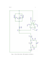
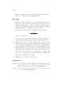
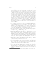
3. Build the op amp phase shift oscillator shown in Figure 1. This is just
the phase shift oscillator of Figure 5 in Appendix C with the same
simple amplitude stabilization used in the Wien bridge. The left-hand
resistance of the POT (between the tap and C3 ) is R in Figure 5 of
Appendix C, and the right-hand resistance plus R2 is the same as the
feedback resistor R1 in Figure 5 of Appendix C.
• Adjust the potentiometer until oscillation is sustained. Record
the oscilloscope display of the output. Measure the oscillation
frequency.
• Measure the potentiometer resistance required to sustain oscillation. Compare with the theoretical values calculated in Appendix C: if Rl is the resistance between C3 and the tap and
Rr is the resistance to the right of the tap, then Rl should be
10 kΩ, (Rr + R2 )/Rl should be greater than 29, and under
√ these
conditions the frequency of oscillation is f0 = 1/(2πRC 6).
• Record the FFT of the output on the oscilloscope.
References
[Sedra/Smith] Adel S. Sedra and Kenneth C. Smith, Microelectronic Circuits, 4th ed., Oxford (1998)
Lab 4
3
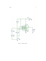
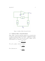
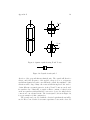
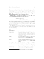
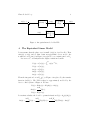
Figure 1: Phase Shift Oscillator With Amplitude Stabilization
LABORATORY 5
AMPLITUDE MODULATED SIGNALS
AND ENVELOPE DETECTION
OBJECTIVES
To take measurements of AM signals in the time and frequency domains,
and to investigate envelope detection of AM signals.
PRELAB
1. Read Section 5-1 (Amplitude Modulation) and Section 4-13 (Detector
Circuits; read “Envelope Detector” subsection) in [Couch], or Section 4.2 (Double-Sideband Amplitude Modulation) and Section 4.5
(especially the subsection on Envelope Detection) in [Carlson].
2. An AM signal is written as
xc (t) = Ac (1 + µx(t)) cos 2πfc t,
where fc is the carrier frequency, Ac is the carrier amplitude, µ is the
modulation index, and x(t) is the baseband message signal. We assume
that x(t) has absolute bandwidth W ¼ fc , and that its amplitude has
been normalized so that |x(t)| ≤ 1.
If x(t) is a cosine of amplitude 1 and frequency fm ¼ fc :
• Obtain an expression for the amplitude spectrum Xc (f ) of the
AM signal xc (t).
• Determine the power in the carrier and in the sidebands. Express
the powers in units of dBm into a 50 Ω load. (Remember that
the spectrum analyzer input impedance is 50 Ω.)
1
Lab 5
2
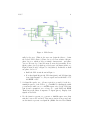
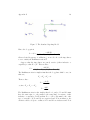
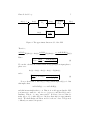
Figure 1: Simple Envelope Detector
• Determine the ratio of the power in the sidebands to the power
in the carrier.
3. Obtain numerical values in Item 2 if fm = 15 kHz, µ = 1/2, and the
carrier amplitude and frequency are Ac = 1 and fc = 300 kHz. Also,
use Mathcad or Matlab to plot the AM signal xc (t).
4. Repeat Item 2 for a message x(t) which is a square wave of amplitude
1, zero dc level, 50% duty cycle, and fundamental frequency fm .
5. Obtain numerical values in Item 4 if fm = 15 kHz, µ = 1/2, and the
carrier amplitude and frequency are Ac = 1 and fc = 300 kHz. Also,
use Mathcad or Matlab to plot the AM signal xc (t).
6. In lab you will display the AM signal on the oscilloscope. Devise a way
to measure the modulation index µ from the plot of the AM signal.
(Hint: consider the maximum and minimum peak-to-peak swings of
the AM signal—look at Figure 5-1(b) in [Couch] or Figure 4.2-1(b) in
[Carlson].)
7. As explained in Section 4-13 of [Couch] or Section 4.5 of [Carlson], an
AM signal with less than 100% modulation (i.e., with µ < 1) can be
easily demodulated using an envelope detector, shown in Figure 1. In
fact, this is the reason for AM—we transmit a large amount of wasted
power in the carrier, but we can use a non-synchronous detector. In
practice, the situation is more complicated: the envelope detector has
very low input impedance, so we need a large resistor at the input; then
voltage division between the input resistor and the envelope detector
causes the output signal level to be unacceptably small, and so we
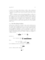
need to amplify it. The envelope detector circuit you will use in lab
is shown in Figure 2. The resistor R1 raises the input impedance to
Lab 5
3
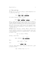
Figure 2: Envelope Detector To Be Used In Lab
Lab 5
4
Figure 3: Using the MULT Part to Generate an AM Signal in PSpice
at least R1 . The envelope detector consists of D1 , R2 , and C2 . The
amplifier is required to overcome voltage division between R1 and the
envelope detector. The R3 -C1 circuit is a high-pass filter to block any
dc in the signal coming from the envelope detector. Suppose that the
AM input signal to the demodulator of Figure 2 is the signal from
Items 2 and 3, in which the message is a cosine wave.
• Show that the bandwidth of the R2 -C2 lowpass filter is appropriate for this AM signal.
• Show that the bandwidth of the R3 -C1 highpass filter is appropriate.
• Calculate the gain of the op amp stage.
• Simulate the demodulator circuit in PSpice. (Hint: You can
generate an AM signal by using the MULT part in the evaluation
library. See Figure 3.)
IN LAB
1. Set the HP/Agilent function generator to produce the AM signal of
Items 2 and 3 in the Prelab. Display the AM signal on the oscilloscope
(watch your impedances).
Lab 5
5
Notes: (1) In AM mode the carrier amplitude is reduced to half the
set value, so you will need to set the carrier amplitude to 4 Vp-p .
(2) You may find it useful to use the SYNC output of the function
generator as a trigger source. The SYNC output is a TTL high pulse
(look at it on the oscilloscope) produced at each zero crossing of the
modulating signal. See the 33120A User’s Guide for more information
about the SYNC output.
2. Measure the modulation index (Item 6 in the Prelab) and check against
the set value on the function generator.
3. Display the spectrum of the AM signal on the spectrum analyzer, in
units of dBm into 50 Ω. Measure the power level of the carrier and
of the sideband line. How many dB below the carrier is the sideband
line? Compare your measurements to your Prelab calculations.
4. Investigate the effect on the AM spectrum of varying the modulating frequency (i.e., message frequency) and the modulation index. In
particular, investigate the effect on the sideband power of varying the
modulation index.
5. Set the function generator so that the message is the square wave of
Items 4 and 5 from the Prelab. Display the AM signal on the DSO
and measure the modulation index.
6. Display the AM signal on the spectrum analyzer. Measure the carrier
and at least five sideband pairs. How many dB below the carrier
are the sideband lines? Compare your measurements to your Prelab
calculations.
7. Build the envelope detector of Figure 2. Apply the AM signal of Item 1
(sinusoidal message) and display the demodulated output on the DSO.
Compare the demodulated signal to the message signal, and comment
on any discrepancies. Investigate the effect of varying the message
frequency and the modulation index.
8. Repeat for the AM signal of Item 5 (square wave message).
Lab 5
6
References
[Carlson] A. Bruce Carlson, Paul B. Crilly, and Janet C. Rutledge, Communication Systems: An Introduction to Signals & Noise in
Electrical Communication, 4th ed., McGraw-Hill (2002)
[Couch]
Leon W. Couch, II, Digital and Analog Communication Systems, 6th ed., Prentice-Hall (2001)
LABORATORY 6
AM MODULATORS
OBJECTIVES
To simulate, build, and test an unbalanced AM modulator, and to simulate
one kind of doubly balanced modulator.
PRELAB
1. Read Section 4.3 in [Carlson] (especially Square Law and Balanced
Modulators), Section 4.11 in [Couch], and Appendix D of this lab
manual.
2. You are going to build and test the very simple unbalanced diode AM
modulator shown in Figure 1. In this circuit, the message is a 30 kHz
sinusoid and the carrier is a 200 kHz sinusoid. The R1 -R2 -R3 network
adds the carrier and the modulating signal, the square-law device is
the 1N4148 diode, and the L1 -C1 -R4 network is the bandpass filter.
The output is the voltage across L1 -R4 to ground, as indicated.
3. Verify that the filter is a bandpass filter (the input is the current into
the filter and the output is the voltage across it), and that its resonant
frequency is the carrier frequency.
4. Simulate the circuit of Figure 1. Run the simulation for a long enough
time that the FFT of the output voltage will be accurate. Reasonable
values for the amplitudes of the sinusoids are 0.8 V for the message
and 1.0 V for the carrier.
5. Display the FFT of the output voltage; include the printout in your
notebook.
1
Lab 6
2
Figure 1: AM Modulator
Lab 6
3
6. Your FFT should show an AM signal at 200 kHz with the sideband
lines 30 kHz above and below. But you will also see other smaller
components. What is their origin? (Two hints: What is the frequency
response of your bandpass filter? Is the diode exactly a square-law
device?)
7. Calculate how many dB below the carrier line (200 kHz) the spurious
lines in the spectrum are.
8. In Item 4 of the In Lab portion you will simulate a doubly-balanced
modulator. You should have time to do that part in lab, but you may
do it as a prelab if you wish.
IN LAB
1. Build the AM modulator of Figure 1. Note. The 2.2 mH inductors
are available, but you cannot get exactly the 287 pF capacitors. But
you can get close by using series or parallel combinations of capacitors
that are available. The resonant frequency of the bandpass filter will
be slightly off. (You may adjust the carrier frequency to match the
resonant frequency of your filter if you like.)
2. Display the output voltage signal on the oscilloscope, and display its
FFT on the oscilloscope.
3. Display the output spectrum on the spectrum analyzer. Compare the
frequencies of the lines you observe with your prelab simulation, and
compare the differences (in dB) of the line amplitudes from the carrier
with your prelab simulation.
4. In this part you will simulate, but not build, one type of doubly
balanced mixer for generation of DSB. Layout the circuit of Figure 2
in Schematics. (This type of doubly-balanced mixer is discussed in
Section 4.11 of [Couch].) The message and the carrier are the same as
in the preceding parts.
5. Run the simulation for what you think would be a good time to get
an accurate FFT. Display the FFT.
6. You should see a prominent carrier line. But isn’t this circuit supposed to produce DSB? This simulation demonstrates a phenomenon
apparent only in the simulation. PSpice starts the simulation at t = 0,
Lab 6
4
Figure 2: DSB Modulator
Lab 6
5
and so the circuit experiences a transient. In this circuit, the BPF resonates at fc = 200 kHz and it is seeing Ac sin(2πfc t)u(t) at the start
of the simulation. As a result, the filter “rings” for a short time and
so a significant line at 200 kHz is seen.
7. You can run a more accurate simulation as follows. (1) From your
simulation, estimate how long the transient lasts. (In my simulation it
lasts about 150–200 µs.) Run the simulation for much longer so that
the output is mostly steady-state. Now look at the FFT. (2) Better
still, in the simulation setup enter a no-print delay large enough so
that the the initial transient data is not collected. Display the output
voltage and its FFT. You should find that the carrier line is suppressed.
8. The moral of this little exercise is that you have to pay attention
to transients in simulations. Sometimes you want to see the transient. But sometimes it is unimportant, and if you don’t set up your
simulation appropriately, you may be misled when you go to make
steady-state measurements on the circuit.
9. One final point. Why did you not build this circuit? (It seems to be
simple enough.) Answer: look at how the carrier must be connected.
Can you connect the function generator this way? The answer is no.
The function generator produces a single-ended output, meaning that
it must be connected between a node and ground. The carrier generator called for in Figure 2 must have a differential output. (It’s
the same sort of reason that you cannot use the oscilloscope probe
to measure the voltage across two nodes—you must always measure
from a node to ground. To measure across nodes you need a differential probe—they are available, but expensive. A 20 MHz differential
probe for our oscilloscopes costs around $500.)
References
[Carlson] A. Bruce Carlson, Paul B. Crilly, and Janet C. Rutledge, Communication Systems: An Introduction to Signals & Noise in
Electrical Communication, 4th ed., McGraw-Hill (2002)
[Couch]
Leon W. Couch, II, Digital and Analog Communication Systems, 6th ed., Prentice-Hall (2001)
LABORATORY 7
THE PHASE-LOCKED LOOP AND
FREQUENCY MODULATION AND
DEMODULATION
OBJECTIVES
To investigate FM signals in the time and frequency domains; to measure
the characteristics of a phase-locked loop (PLL); to use a PLL for frequency
modulation and demodulation.
PRELAB
Prelab
1. Read Section 5-6 (Phase Modulation and Frequency Modulation) and
Section 4-14 (Phase-Locked Loops and Frequency Synthesizers) in
[Couch], or Sections 5.1 (Phase and Frequency Modulation) and 5.2
(Transmission Bandwidth and Distortion) and Section 7.3 (Phase-Lock
Loops) in [Carlson], and Appendix E (The Phase-Locked Loop) in this
manual.
2. Obtain an expression for the spectrum of an FM signal with single-tone
modulation, where the carrier amplitude is Ac , the carrier frequency
is fc , the message frequency is fm , and the modulation index is β.
• For such an FM signal, what is the smallest value of β for which
the carrier spectral component is zero?
• Plot the FM spectrum for the following values: Ac = 100 mV,
fc = 100 kHz, fm = 10 kHz, and β = 1. Express the amplitudes
of the lines in units of dBm into 50 Ω.
• For these values, use Carson’s rule to estimate the FM bandwidth.
1
Lab 7
2
• Determine the 99% power bandwidth of the FM signal. (That is,
the frequency band containing 99% of the total power.)
• Finally, plot the FM signal in the time domain. Hint: In Mathcad, use the following to calculate the Bessel functions: J0(x)
returns J0 (x), J1(x) returns J1 (x), and Jn(m,x) returns Jm (x)
for 0 ≤ m ≤ 100. In Matlab, use BESSELJ.
• Repeat for β = 3.25.
3. Design an RC lowpass filter having half-power bandwidth between
1.5 kHz and 2.5 kHz (the lower the cutoff frequency the better), and
having R ≥ 10 kΩ. You will use this filter in the PLL demodulator
part of the lab.
IN LAB
1. Use the function generator to produce a tone-modulated FM signal
with a sine wave carrier having the following parameters: carrier frequency fc = 100 kHz, carrier amplitude Ac = 100 mV, message frequency fm = 10 kHz, and modulation index β = 1. (You set β by
setting the peak frequency deviation on the function generator.)
2. Display the FM signal on the DSO.
3. Display the FM signal on the spectrum analyzer.
• Measure the frequencies and power levels (in dBm) of the carrier
and the first five lines above the carrier. Compare with your
prelab.
• Use the spectrum analyzer to measure the 99% power bandwidth
of the FM signal. Compare with your prelab bandwidth calculations and with the Carson’s rule bandwidth.
4. Repeat items 1, 2, and 3 with an FM signal having modulation index
β = 3.25.
5. Keeping the carrier frequency and the message frequency fixed, investigate the effect on the FM spectrum of changing the modulation index.
Determine the smallest frequency deviation for which the carrier power
is zero and compare to your prelab.
Lab 7
3
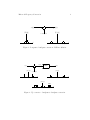
Figure 1: Block Diagram of the CD4046 PLL
6. We shall now study the characteristics of a particular phase-locked
loop. The CD4046 is a digital PLL chip implemented with CMOS
technology; the block diagram of the chip is shown in Figure 1.1 Any
PLL consists of three blocks: a phase detector (or phase comparator), a low-pass filter, and a voltage-controlled oscillator (VCO). (See
Figure 4-19 in [Couch] or Figure 7.3-2 in [Carlson], and Figure 2 in
Appendix E of this manual.) The CD4046 provides two different phase
detectors and the VCO; the lowpass filter must be connected exter1
Specification data for the CD4046 PLL, National Semiconductor Corp., Document
no. RRD-B30M115, (1995).
Lab 7
4
Figure 2: PLL Circuit
nally by the user. (That is, the user can design the filter to obtain
the desired PLL behavior.) Phase detector I is an exclusive OR gate
phase detector, which provides a triangle characteristic , and phase
detector II is an edge controlled memory network (essentially, it is a
flip-flop phase detector) which provides a sawtooth characterisitic; see
Figure 4-20 in [Couch] or Figure 7.3-1 in [Carlson]. In this lab we shall
use phase detector I.
• Build the PLL circuit shown in Figure 2.
• Note that Signal In (pin 14), VCO Out (pin 4), and PC1 Out (pin
2) are digital signals—i.e., they are square waves with LOW = 0 V
and HIGH = 10 V.
7. Set Signal In equal to zero. (Connect pin 14 to ground.) Set the freerunning frequency of the VCO to f0 = 100 kHz by adjusting the 20 kΩ
potentiometer until you see a 100 kHz square wave at the VCO Out
(pin 4) and a symmetric error voltage (i.e. equal LOW and HIGH
durations) at the Phase Comparator I output (pin 2). Display both
signals on the DSO.
8. Use the function generator to generate a 100 kHz square wave that
switches between 0 V and 10 V. Disconnect pin 14 from ground, and
use the function generator as Signal In. (Note: Pin 14 of the CD4046
Lab 7
5
Figure 3: Typical PLL Waveforms in Locked Condition
is a high impedance input.) Display and print the signals at PC1 Out
(pin 2), Comparator In (pin 3), VCO In (pin 9), and Signal In (pin 14).
(Typical waveforms that you should see are shown in Figure 3.) Be
sure to record the voltage levels and frequencies of the signals. Note:
You may use the Signal In to trigger the DSO.
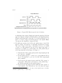
9. We shall next measure the hold-in and pull-in ranges of the PLL.
(Refer to Figure 4-23 and the accompanying discussion in [Couch].)
The hold-in range is the range of frequencies about f0 over which
a locked loop will remain in lock; the pull-in range is the range of
frequencies over which a loop will acquire lock.2 The pull-in range is
never larger than the hold-in range; see Figure 4.
• Verify that the VCO output (pin 4) and the input signal (pin 14)
are both at f0 = 100 kHz.
• Set the input frequency to a value below f0 such that the PLL is
out of lock; when the loop is out of lock the VCO output signal
will be unstable.
• Slowly increase the input frequency until the VCO output becomes stable. This is the lower frequency of the pull-in range—
the PLL has just pulled-in the input frequency.
• Slowly increase the input frequency until the VCO output becomes unstable. The PLL has now lost lock; this is the upper
2
The hold-in range is also called the lock range, and the pull-in range is sometimes
called the acquisition range or capture range.
Lab 7
6
∆fh
∆fh
-
∆fp
-
∆fp
-
-
fin
f0
Figure 4: Pull-in and Hold-in Ranges: Pull-in = 2∆fp , Hold-in = 2∆fh
frequency of the hold-in range.
• Slowly decrease the input frequency until the PLL again acquires
lock—this is the upper frequency of the pull-in range.
• Continue decreasing the input frequency until the PLL loses lock—
this is the lower end of the hold-in range.
• The device manufacturer gives the following approximate relationship between the hold-in and pull-in ranges3 :
r
2∆fh
2∆fp ≈
.
πR3 C2
Compare your measured values to this formula.
10. We shall now use the PLL as an FM modulator; build the circuit
of Figure 5. Set the free-running frequency of the VCO (pin 4) to
100 kHz; see item 7.
• Use one function generator to produce a 100 kHz square wave
that switches between 0 V and 10 V. Use this for the Carrier In
signal (pin 14).
• Use your second function generator to produce a 1 kHz, 5 Vp-p
sine wave. Use this for the Message Signal.
• Display the FM signal (the VCO output at pin 4) on the DSO.
• Systematically investigate the effect on the FM signal of varying
the amplitude and frequency of the message signal. Explain your
observations.
11. We shall now use the PLL as an FM demodulator; build the circuit of
Figure 6. Set the free-running frequency of the VCO to 100 kHz.
3
Specification data for the CD4046, op. cit., p.11
Lab 7
7
Figure 5: FM Modulator Circuit
• Use the function generator to produce the following FM signal.
Carrier: sine wave at 100 kHz, 10 Vp-p with 5 V dc offset; this is
the Carrier In signal on pin 14. (The dc offset must be present
because the pin 14 signal must have LOW level 0 and HIGH level
10 V.) Message: sine wave at 1 kHz. Peak frequency deviation:
1 kHz. This is the Message Signal input in Figure 6. Connect
the RC lowpass filter from the second week prelab to pin 2 as
indicated in Figure 6.
• Display the demodulated signal (output of the LPF) on the DSO.
Hint: Use the SYNC output of the function generator for your
trigger.
• Investigate the effect of varying the frequency of the message
signal, and explain your observations.
Lab 7
8
Figure 6: FM Demodulator Circuit
References
[Carlson] A. Bruce Carlson, Paul B. Crilly, and Janet C. Rutledge, Communication Systems: An Introduction to Signals & Noise in
Electrical Communication, 4th ed., McGraw-Hill (2002)
[Couch] Leon W. Couch, II, Digital and Analog Communication Systems, 6th ed., Prentice-Hall (2001)
LABORATORY 8
MORE FREQUENCY
MODULATION/DEMODULATION
OBJECTIVES
To investigate direct FM using a VCO and slope detection of FM.
PRELAB
1. Read Sections 4-13 and 5-6 in [Couch], or Section 5.3 in [Carlson] on
direct generation of FM, and slope detection of FM.
2. There are many ways of generating and detecting FM; we saw one in
Laboratory 7 using a PLL. In this lab we shall consider one method
of direct FM using a voltage-controlled oscillator (VCO). A VCO is
also an integral part of the PLL. We shall use the popular 555 timer
IC as the VCO in this lab. The 555 is basically a multivibrator; it can
be operated in monostable mode (i.e., as a “one-shot”) or in astable
mode as an oscillator. When used as an oscillator it of course provides
a square wave output.1
The FM modulator is shown in Figure 1. The message is the sinusoidal
source labeled VMod; it has an amplitude of 1 V and a frequency of
5 kHz. The DC offset Voff must be present because the 555 control
input must always be positive. (You may of course set the offset in
the sinusoidal source.) Simulate the modulator and display the output
and its spectrum. (Remember that you are looking at tone modulation
of a square carrier.) Is the spectrum what you expect?
1
See the 555 data sheet for further details: LM555 Timer Specifications, National
Semiconductor Corp., February 2000.
1
Lab 8
2
Figure 1: FM Modulator
Lab 8
3
Figure 2: FM Slope Detector
3. The demodulator is the simple slope detector of Figure 2. This is an
FM-to-AM converter—it differentiates the FM signal and passes the
resulting mixed FM/AM signal through an envelope detector. The
front end is a tuned bandpass filter; its resonant frequency is slightly
higher than the carrier frequency so that the incoming FM signal lies
on the left side of the filter frequency response so that it acts as a
differentiator. The diode and R4 -C3 circuit is of course the envelope
detector, and the C4 -R5 circuit is the highpass filter (DC block).
• Calculate the resonant frequency of the bandpass filter.
• Calculate the time constant of the lowapss filter in the envelope
detector and show that it is appropriate for the message and
carrier frequencies.
• Calculate the time constant of the highpass filter and show that
it is appropriate.
4. Connect the FM modulator of Figure 1 to the slope detector of Figure 2 and simulate the whole system. (Remove the load resistor in
Figure 1—connect the output directly to the FM Input in Figure 2.)
Display the output and its FFT. (Note: As always, you will want
to run the simulation for a long enough time to get good FFT; you
will also see that the output has a transient before it settles into a
steady-state that you will probably not want to include in the FFT.
But, if you try to run the simulation for too long, you will encounter
a limitation of the evaluation version of PSpice—the 555 is a mixed
analog/digital part and if you try to run the simuation for too many
periods of the square wave output you will find a limitation on the
Lab 8
4
number of transitions allowed in the digital circuit. You will have to
find a good compromise for the simulation time.)
IN LAB
1. Build the circuit of Figure 1 without the modulating signal and its
DC offset—replace them with a small capacitor. This is the freerunning astable circuit; the output across the load resistor will be a
square wave. Display the output and its spectrum and measure its
fundamental frequency. This square wave is the carrier.
2. Compare the measured frequency against the theoretical value
fc =
1.44
.
(R1 + 2R2 )C1
(See the 555 data sheet.)
3. Now connect the message (with DC offset) as in Figure 1. Display the
output and its spectrum; compare with your prelab simulation.
4. Build the slope detector of Figure 2. Test the slope detector by using
the function generator to provide an FM signal of the same carrier
frequency and tone modulating frequency as your 555 FM modulator.
Choose the frequency deviation to give you approximately the same
FM bandwidth as your 555 modulator. You can test with sinusoidal
and square carriers. Display the demodulated output and its spectrum.
5. Now connect the output of the 555 modulator to the input of the
slope detector. (Remove the load resistor in Figure 1.) Display the
demodulated output and its spectrum.
6. Explain sources of distortion in the detector.
References
[Carlson] A. Bruce Carlson, Paul B. Crilly, and Janet C. Rutledge, Communication Systems: An Introduction to Signals & Noise in
Electrical Communication, 4th ed., McGraw-Hill (2002)
[Couch]
Leon W. Couch, II, Digital and Analog Communication Systems, 6th ed., Prentice-Hall (2001)
LABORATORY 9
SAMPLING AND PULSE AMPLITUDE
MODULATION
OBJECTIVES
To investigate the time- and frequency-domain properties of PAM signals
with natural sampling.
PRELAB
1. Review the discussion of the sampling theorem in Section 2-7 of [Couch]
and Section 6.1 of [Carlson].
2. Read Section 3-2 in [Couch] about flat-top sampled PAM and naturally
sampled PAM. (Section 6.2 in [Carlson] discusses only flat-top PAM,
but naturally sampled PAM was discussed in lecture.)
3. Consider a sinusoidal message signal
x(t) = A0 cos(2πf0 t).
Suppose we create a naturally sampled PAM waveform, xs (t), using
a sampling waveform having sampling frequency fs and duty cycle
d = τ /Ts . (See Figure 3-1 in [Couch].) Assume that fs exceeds the
Nyquist rate for x(t).
If f0 = 500 Hz, fs = 5 kHz, τ = 40 µs, and A0 = 1 V:
• Calculate and plot the PAM signal xs (t),
• Calculate and plot the magnitude spectrum |Xs (f )|.
1
Lab 9
2
You may of course make the plots carefully and to scale by hand on
graph paper, but it will be much easier and more efficient to use Mathcad or Matlab. You should use the FFT function in these programs
to obtain the plot of |Xs (f )|.
4. In lab you will implement naturally-sampled PAM using an electronic
switch. Specifically, you will use the CD4016 CMOS quad bilateral switch. Simulate the circuit of Figure 1 in PSpice. The part
CD4016BD is available in the EVAL library of Microsim PSpice—the
message is applied to pin 1, the sampling waveform is applied to pin
13, +Vcc is applied to pin 14, −Vcc is applied to pin 7, and the PAM
output is on pin 2. Use a sinusoidal message and a sampling waveform
as in Item 3. Set the amplitude of the sampling waveform for a ±Vcc
swing. Plot the PAM output signal and its spectrum using the FFT
in Probe.
Hint: I suggest using the VPULSE part in PSpice to generate the
sampling waveform. You need to specify the rise time and fall time of
this square wave. You can also specify a maximum time step in the
Analysis Setup. Your PAM signal will probably look “spikey”. This is
caused partly by how you adjust the rise and fall times relative to the
maximum step size. You can reduce this effect (but you may not be
able to eliminate it) by making the maximum step size small relative
to the rise and fall times of the sampling waveform. Of course, the
smaller you make the step size the longer the simulation will take.
As the engineer on this project, you will have to reach a reasonable
compromise.
5. The message x(t) can be recovered from the PAM signal by ideal lowpass filtering. (This is explained in [Couch] and in lecture.)
Of course we do not have an ideal LPF. Suppose that we recover the
sinusoidal signal from the PAM signal in Item 3 by means of a nonideal low-pass filter. To be exact, we shall use the Sallen-Key circuit
from Laboratory 3 with R = 30 kΩ and C = 0.01 µF (which result in
6 dB break frequency of 530 Hz). Calculate and plot the signal and
its amplitude spectrum at the filter output. (Again, you should use
Mathcad or Matlab.)
The demodulated output of the filter will not be precisely the sinusoidal message that you started with—there will be some other frequency components present. In other words, the demodulated output
signal will be distorted. This distortion is not nonlinear distortion,
Lab 9
3
Figure 1: Generation of naturally sampled PAM
but is present simply because the filter is not an ideal LPF—it passes
some unwanted frequency components. As we have seen (in Lab 3),
one fairly quick way to quantify the distortion is to calculate the total
harmonic distortion. Calculate the THD of the demodulated signal at
the output of the filter.
6. Simulate the demodulation of the PAM signal in PSpice: connect the
output of the PAM circuit to the input of the Sallen-Key circuit. Plot
the demodulated output of the filter in Probe and its spectrum.
Also calculate the THD of the demodulated signal in this simulation.
IN LAB
1. Build the circuit shown in Figure 1. This circuit implements the naturally sampled PAM system shown in Figure 3-2 of [Couch]—the signal
to be sampled is the input to a switch, the opening and closing of
which is controlled by the sampling signal consisting of a sequence
of rectangular pulses. The CD4016 is a quad analog CMOS bilateral
Lab 9
4
switch. (That is, there are four switches on the chip, and on each
switch the signal flow can be in either direction.) Pins 1, 2, and 13
constitute one switch: pins 1 and 2 are the input and output, and pin
13 is the on/off control signal. The other pins that are tied low (pin 7
is ground) are the inputs and controls of the other three switches; the
open pins are the outputs of the other three switches. These pins must
be connected as indicated to prevent crosstalk. You should understand
that the device is a switch, but it is not an ideal switch. In particular,
it has a non-zero propagation delay from input to output (approximately 15 ns), non-zero “on” resistance (approximately 215 Ω), and
its frequency response is not flat (it has a 3 dB break frequency of
about 150 MHz).1
2. Set one function generator to produce the rectangular sampling waveform with parameters fs and τ from item 3 of the Prelab. Set the
amplitude of the sampling signal for ±Vcc swing. Pay attention to
how you connect the function generator to the circuit—what should
you set the output impedance of the function generator to?
3. Use the other function generator for the sinusoidal message signal to
be sampled—set f0 = 500 Hz and A0 = 1 V.
4. Display the PAM signal on the oscilloscope. (It may help to get your
trigger off the message signal.) Is its amplitude what you expect?
Explain. (Remember: the switch is not ideal.) To make measurements
easier, adjust the message signal amplitude so that the PAM signal has
swing 2 Vp-p . Include a printout of the PAM signal in your notebook.
5. Display the spectrum of the PAM signal on the oscilloscope. Include
a printout of the spectrum in your notebook.
6. Record the magnitudes of the spectral components of the PAM signal,
and record the ratios (or differences in dB) between adjacent peaks.
Compare with your prelab item 3 PAM spectrum.
7. Now connect the PAM output signal to the input of the Sallen-Key
filter with cutoff fc = 530 Hz. Display the demodulated signal on the
oscilloscope, and include a printout in your notebook. Is it what you
expect?
1
“Motorola Semiconductor Technical Data: MC54/74HC4016, Motorola, Inc., 1995.
Lab 9
5
8. Display the spectrum of the demodulated signal on the oscilloscope
and include a printout in your notebook. Measure the magnitudes,
and differences in magnitudes, of any spectral peaks, and compare
with your calculations from item 5 of the prelab.
9. Calculate the THD of the demodulated signal and compare with your
prelab.
10. Investigate systematically the effect of sampling pulse duration τ (or
duty cycle d) and sampling rate fs on the PAM signal and on the
demodulated signal. Record your observations systematically and
quantitatively. Compare your observations to what you should expect
the effects to be in theory. Be sure to decrease fs below the Nyquist
rate so that you can observe aliasing.
References
[Carlson] A. Bruce Carlson, Paul B. Crilly, and Janet C. Rutledge, Communication Systems: An Introduction to Signals & Noise in
Electrical Communication, 4th ed., McGraw-Hill (2002)
[Couch]
Leon W. Couch, II, Digital and Analog Communication Systems, 6th ed., Prentice-Hall (2001)
LABORATORY 10
ISI and Eye Patterns
Overview
Prelab
•
The goal of the prelab will be to use simulation to generate an eye pattern
for a binary or 4-ary PAM signal. The eye pattern will be observed for
several different roll-off factor values. This will be a multi-step problem:
1. Generate a random PAM signal
2. Generate a Raised Cosine filter (pulse)
3. Run the PAM signal through the Raised Cosine filter
4. Plot the Eye Pattern
5. Display the Fourier transform of the output
In-Lab
•
The goal of the in-lab portion of the experiment is to observe an eye
pattern on the oscilloscope that is formed by running a PAM signal
through a low-pass filter. This is also a multi-step problem:
1. Generate a pseudo-random PAM signal using the arbitrary function
generator
2. Build an RC filter
3. Run the PAM signal through the RC filter
4. Plot the output eye pattern onto the oscilloscope
5. Display the PSD of the output.
Prelab
1.
Read the section in the book pertaining to ISI and eye pattern diagrams.
(Carlson/Crilly/Rutledge Secs. 11.1 and 11.3, Couch Sec. 3-6)
2.
Generate a random 4-ary PAM signal (at least 100 symbols). Display the
random PAM sequence on a stemplot.
• The following Matlab code will do this, or you can write your own to
achieve the same result:
a=[-3 -1 1 3];
%Create the 4-ary constellation
ind=floor(4*rand(100,1))+1;
%Create a Random bit Sequence
PAM=a(ind);
%Random 4-PAM sequence
stem(PAM);
%Plot Sequence
3.
Generate a raised cosine filter impulse response. The bandwidth is 6kHz.
What condition must we impose on the sampling frequency and why?
We will use a sampling frequency of 27kHz. Assume that we use a
symbol rate of 9000symbols/s. What is the rolloff factor (α)? Consider
the raised cosine from -5T to 5T where T is the symbol period. Plot the
raised cosine filter. Note: the rolloff factor α is a parameter between 0 and 1.
Carlson, et. al., (Sec. 11.3) use parameters β and r to define the raised cosine
filter: the relationship is α=2βT, and r =1/T is the rate. Couch (Sec. 3-6) uses
a parameter fΔ in the raised cosine definition; his fΔ is the same as Carlson’s β,
or α=2fΔT.
Matlab code:
Fs = 27000;
%Sampling frequency is 27kHz
T = 1/9000;
%Symbol period
t=-5*T:1/Fs:5*T;
%Set time scale
t=t+1e-10;
%So that t=0 is not included
alpha=0.5;
%Set roll-off factor
p=(sin(pi*t/T)./(pi*t/T).*cos(alpha*pi*t/T)./(1-(2*alpha*t/T).^2));
%p is the raised cosine pulse
clf;
plot(t,p);
%plot the filter
hold on;
stem(t,p); xlabel(‘Time [s]’); ylabel(‘Amplitude’);
hold off;
4.
Run the PAM sequence through the raised cosine filter. Remember that
to use the ‘filter’ function in Matlab, the two vectors must have the same
sampling frequency, so it will be necessary to upsample the PAM vector
(i.e., [a1 a2 a3] becomes [a1 0 0 a2 0 0 a3 0 0]).
N=length(PAM);
r=Fs*T;
pams=zeros(size(1:r*N));
pams(1:r:r*N) = PAM;
% upsampled version of PAM
xn=filter(p,1,pams);
%runs vector pams through filter p
figure; plot(xn(1:200));
%plots a portion of the filter output
clf;
hold on;
5.
Generate the eye pattern. Remember that eye patterns are typically
shown over a time period of 2T. Is there a delay to the signal? If so,
why? Now change α (rolloff) to various values between 0 and 1. Make
eye diagrams for several different rolloff factors. How does the rolloff
factor affect the ISI as seen through the eye diagram? How does the eye
diagram show the effect of ISI on sensitivity to timing error and the noise
margin? What is the primary negative effect of high ISI?
d=5*T*Fs+1;
%calculating delay
for i=d:6:300-6
%start from point 16 (delay)
plot(xn(i:i+6))
end
6.
%plot the first 7 samples (2T)
%the loop will plot on top of itself
Experiment with the spectral characteristics of the system. Using 2048
samples, generate frequency spectrum plots for both the filter and the
output signal. Print out both the Signal spectrum of the output and the
filter (in amplitude and dB). How does changing the roll-off factor of the
pulse-shaping filter affect the signal spectrum of the output and the
filter? Make printouts to substantiate your assertions.
Nfft=2048;
P=fftshift(fft(p,Nfft));
%Displays the fft of p
X=fftshift(fft(xn,Nfft));
%Displays the fft of xn
f=-Fs/2:Fs/(Nfft-1):Fs/2;
%Frequency axis scale
figure;
subplot(211);plot(f,abs(P));grid;title('Signal Spectrum of P');
xlabel('Frequency [Hz]');
subplot(212);plot(f,20*log10(abs(P)));grid;title('Signal Spectrum in dB');
xlabel('Frequency [Hz]');
figure;
subplot(211);plot(f,abs(X));grid;title('Signal Spectrum of X');
xlabel('Frequency [Hz]');
subplot(212);plot(f,20*log10(abs(X)));grid;title('Signal Spectrum in dB');
xlabel('Frequency [Hz]');
In-Lab
1. Using Matlab, generate a random binary bit pattern with length 15.
2. Use the function generator to create and store this signal. Because we can
not create a truly random signal, the idea is that we will create a ‘pseudorandom’ signal. By using 15 random bit values repeated at the proper
frequency, we will be able to control the symbol rate. Instructions on
how to create an arbitrary function can be found in the instruction
manual.
3. Design and build an RC filter with the same bandwidth as the raised
cosine filter of the prelab, 6kHz. Record the values of your Resistor and
Capacitor.
4. The symbol frequency is still 9kHz. Set the output of the function
generator accordingly and attach the signal to the filter.
5. Display the eye pattern on the oscilloscope. What effect does changing
the symbol rate have on ISI? Demonstrate your results with
experimentation and commentary.
APPENDIX A
BASICS OF THE DIGITAL STORAGE
OSCILLOSCOPE
1
Introduction
This appendix contains basic information about digital storage oscilloscopes
in general, and some specific information about the Agilent 54622D oscilloscope that you will use in the communication laboratory.
The function of any oscilloscope of course is to provide a visual display
of a time-varying signal (i.e. voltage). In an analog oscilloscope the signal
is directly displayed on a cathode ray tube—an internally generated ramp
causes the electron beam to scan horizontally across the CRT, and the signal
being measured is applied across the vertical deflection plates. In a digital
storage oscilloscope (DSO), the signal is acquired in an entirely different way.
In order to understand the advantages and limitations of a DSO, we must
begin with an understanding of the way in which the oscilloscope acquires
the signal.
2
Signal Acquisition in a DSO
In broad terms, a DSO first samples the input signal and then displays the
waveform that is reconstructed from the samples. This analog-to-digital
conversion performed by the DSO results in several advantages over an analog oscilloscope. The major advantage is that we can perform signal processing operations on the sampled signal, such as differentiation, integration,
addition of signals, calculation of Fourier transforms, as well as storage of
the waveform in memory. At the same time, the digital-to-analog conversion
has its limitations, and you must be aware of these as you make measurements; if you are not careful, the signal you display (i.e. the reconstructed
signal) may not bear any resemblance to the true signal.
1
Appendix A
2.1
2
Sampling
The idea of sampling is simple: take samples of a signal at discrete time
instants, and if the samples are “close enough” in time the signal can be
reconstructed (at least approximately) by interpolating between the samples.
The famous sampling theorem1 tells us precisely how close is “close enough”:
if the samples occur at a rate at least twice the highest frequency contained in
the signal, then the signal can be exactly reconstructed from its samples by
passing the sampled signal through an ideal lowpass filter whose bandwidth
is equal to the highest frequency contained in the signal.
The sampling theorem implies the trade-off that we always face in analogto-digital conversion: we want closely spaced samples, but the more closely
they are spaced, the more samples we need, and hence the more memory
we need to hold them. In most practical problems, memory is the critical
limitation. Hence, we usually start not by specifying the sampling rate,
but by specifying the total number of samples that we will take; this is the
record length. We then select (or more accurately, the oscilloscope selects)
the appropriate sampling rate for the signal. Note how the sampling tradeoff appears now: with a fixed record length, we will only acquire a short time
duration of a rapidly varying signal, while we will acquire a longer duration
of a slowly varying signal.
The Agilent 54622D has a maximum sampling rate of 200 Msamples/sec
for one channel and 100 Msamples/sec for two channels, and a maximum
memory of 4 Mbytes. When you set the horizontal time base, the oscilloscope chooses the sampling rate and the record length (hence the memory
depth). There are some complications in the relationship—under some circumstances the sampling rate can be faster than the rate at which samples
are stored. This is handled internally by a smoothing operation. The signal
frequencies used in this lab should not cause any difficulties. But you should
always be aware of the sampling rate that the instrument is using. (Press
the Main/Delayed button to see it.)
2.2
Acquisition Modes
Now you have the basic idea of the operation of a DSO: take a finite record
length of samples of a signal, and display the time signal reconstructed from
the samples.
There are many aspects of the signal acquisition that you can control,
the main being the choice of acquisition mode. See the manual for more
1
The sampling theorem is discussed in detail in the lecture course, EEL 4514.
Appendix A
3
information.
• Normal Mode. This is the default. The oscilloscope creates a record
by saving the first sample (of perhaps several) during each acquisition
interval.
• Peak Detect Mode. Any signal wider than 5 ns will be displayed
regardless of sweep speed.
• Average Mode. The DSO acquires data after each trigger using
Normal mode, and then averages the record point from the current
acquisition with those stored from previous acquisitions. This mode
helps reduce random noise.
• Real Time Mode. The oscilloscope produces the waveform from
samples collected during one trigger. It should only be necessary at
sweep speeds of 200 ns/div or faster.
You also control signal acquisition with the RUN/STOP and SINGLE
buttons.
3
Triggering
Another important function that you need to learn how to control is triggering; basically, triggers determine when the DSO will start acquiring and
displaying a waveform. That is, the trigger determines the time-zero point.
Once a trigger occurs, the DSO acquires samples to construct the posttrigger (to the right, or after in time) part of the waveform. (The DSO
automatically acquires enough samples to fill in the pre-trigger part of the
waveform.) The oscilloscope will not recognize another trigger until the
acquisition is complete.
3.1
Trigger Source
You can obtain your trigger from one of the input channels, from the AC
power line (useful for testing signals related to the power line frequency,
such as when you are testing a power supply), or from an externally supplied
source (for example, you can use the SYNC signal produced by the function
generator as the trigger source).
Appendix A
3.2
4
Trigger Types
The DSO has several types of triggers that you can use. The default type,
and the only type you will need in this course, is the Edge type. An edge
trigger occurs when the trigger source passes through a specified voltage
level in a specified direction (i.e. slope).
The other trigger types available are pulse, pattern, CAN, duration, I2 C,
sequence, SPI, TV, and USB. You can find details in the DSO user manual.
3.3
Trigger Modes
The mode determines what the DSO will do in the absence of a trigger.
There are three modes.
• Normal. In this mode the DSO will acquire a waveform only when
the trigger conditions are met.
• Auto. This mode will allow the DSO to acquire a waveform even if
a trigger does not occur. In auto mode, a timer starts after a trigger
occurs; if another trigger is not detected before the timer runs out,
the oscilloscope forces a trigger. The duration of the timer depends on
the time base setting. Note that if triggers are being forced, successive
acquisitions will not be triggered at the same point on the waveform,
and so the waveform will not be synchronized on the screen—it will
roll across.
• Auto Level. Works only when edge triggering on analog channels or
external trigger. The oscilloscope first tries to Normal trigger. If no
trigger is found, it searches for a signal at least 10% of full scale on the
trigger source and sets the trigger level to the 50% amplitude point.
If there is still no signal present,the oscilloscope auto triggers. This
mode is useful when moving a probe from point to point on a circuit
board.
3.4
Other Aspects of Triggering
Holdoff When the DSO sees a trigger, it disables the trigger system until
the acquisition is complete. Some repetitive signals, especially digital pulses,
contain many valid trigger points; a simple trigger might result in a series
of waveforms on the screen. You can set the holdoff time to be longer than
the acquisition interval to get a stable display.
Appendix A
5
Coupling Coupling determines what part of the trigger signal is passed
to the trigger circuit. Your choices are DC (all of the signal), AC (the dc part
is blocked), low frequency rejection (frequencies below 50 kHz are blocked),
TV, high frequency rejection (frequencies above 50 kHz are blocked), and
noise rejection (makes the trigger circuit less sensitive to noise, but may
require a higher amplitude signal to trigger).
4
Signal Spectra on the DSO
As we have said, one very useful feature of the DSO is its ability to display
the results of mathematical operations on the signals. Your Agilent 54622D
can display the product of the two channels, the difference between the
channels, the derivative of a signal, the integral of a signal, and the amplitude
spectrum of a signal. Here we shall discuss the display of the spectrum.
The DSO calculates the spectrum by calculating the discrete Fourier
transform (DFT) of the signal.2 To be precise, the oscilloscope calculates
the fast Fourier transform (FFT), which is just an efficient algorithm for the
DFT. It is important that you have a basic understanding of how the DSO
calculates the FFT, because it is possible that it will display utter gibberish
(as any computer will) if you do not understand its limitations. The basic
idea is this3 : we wish to calculate the Fourier transform of a continuous-time
signal on a digital computer, so we first truncate the signal to a finite-time
duration by multiplying it by a “window” function, and then we sample
the windowed time function at an appropriate rate to create a finite-length
record of samples. Suppose that x(t) is the waveform, and after windowing
and sampling we have N samples, say x0 , x1 , . . . , xN −1 . The DFT of the
samples is defined by the equation
X(k) =
N −1
1 X
xn e−j2πnk/N ,
N
k = 0, 1, . . . , N − 1,
n=0
and the inverse DFT is
xn =
N
−1
X
X(k)ej2πkn/N ,
n = 0, 1, . . . , N − 1.
k=0
2
The DFT is similar, but not identical, to the discrete-time Fourier transform for
discrete-time signals that you learned about in EEL 3135.
3
See Section 2–8 of Couch’s book.
Appendix A
6
Note that the DFT X(k) is a discrete-frequency function; if we select the
windowing function correctly and if we sample at the appropriate rate, X(k)
will be a good approximation to the Fourier transform X(f ).
We shall not go into details about the DFT here; for now we shall merely
state some of the limitations about using the DFT as an approximation to
the continuous Fourier transform that you should keep in mind. These limitations are summarized in the conditional statement we made earlier: if we
select the windowing function correctly and if we sample at the appropriate
rate, X(k) will be a good approximation to the Fourier transform X(f ).
• Regardless of the number of points in the waveform record, the Agilent
DSO uses 2048 points for the FFT.
• Three windows are available: Hanning, rectangular, and flat-top. See
the User’s Guide for advice on using windows.
• Note that the vertical units for the FFT display are dBV.
• It would be to your benefit to read “FFT Measurement Hints” on pages
5-29–5-30 in the User’s Guide, especially the discussion of frequency
resolution.
Always remember: Every time you make a measurement with
an oscilloscope, you must know how the input is coupled, how the
waveform is acquired, how the oscilloscope is triggered, and the
sampling rate being used.
APPENDIX B
BASICS OF THE SPECTRUM
ANALYZER
1
Introduction
This appendix contains some general information about spectrum analyzers,
and some specfic information about the Agilent E4411B spectrum analyzer
that you will use in the communication laboratory. Remember that the
spectrum analyzer User’s Guide is included in the “Equipment Manuals”
folder on the PC desktop at your lab station.
Like an oscilloscope, a spectrum analyzer produces a visible display on a
screen; the Agilent spectrum analyzer has a VGA screen rather than a CRT
screen. Unlike an oscilloscope, however, the spectrum analyzer has only
one function—to produce a display of the frequency content of an input
signal. (But it is possible to display the waveform on the spectrum analyzer
screen with the proper settings.) And also like an oscilloscope, the spectrum
analyzer will always produce a picture on the screen; but if you do not know
how to properly use the spectrum analyzer, that picture may be complete
gibberish.
CAUTION: The input of the spectrum analyzer cannot tolerate
large signals; before you connect a signal to the input, be sure you
know that the signal will not exceed the maximum allowable input
rating of the spectrum analyzer. (The maximum signal input is
printed right on the front panel, near the input connector.)
2
Signal Acquisition in a Spectrum Analyzer
Most spectrum analyzers (including the Agilent models in the communication lab) are heterodyne 1 spectrum analyzers (also called scanning spec1
Heterodyne is derived from the Greek, meaning mixing different frequencies
1
Appendix B
x(t)
2
- ×
6
Fixed
- Narrowband
-
Filter
*
∼
cos 2πf0 t
Figure 1: Frequency Mixing, or Heterodyning
trum analyzers). A heterodyne analyzer is essentially a radio receiver (a
very sensitive and selective reciever). Radio receivers, including those based
on the heterodyne principle, are covered in some detail in the lecture course
(see Section 4–16 in [Couch] or Section 7.1 in [Carlson]); for now we shall
content ourselves with a simple description of the basic ideas.
Given a voltage signal x(t), how do we resolve it into its frequency components for display on a screen? As we know, one solution is provided by
the digital storage oscilloscope—calculate the FFT of the signal from its
internally stored samples. Another solution would be to pass x(t) through a
bank of very narrow bandpass filters, having adjacent passbands, and then
plot the amplitudes of the filter outputs. That is, if filter 1 has passband
f1 −B/2 ≤ f ≤ f1 +B/2, and filter 2 has passband f2 −B/2 ≤ f ≤ f2 +B/2,
where f1 + B/2 = f2 − B/2, and so on, and if B is small enough, then the
filter outputs give us the frequency components X(f1 ), X(f2 ), . . .. This is, of
course, not a practical solution. A better solution is suggested by a simple
property of Fourier transforms: recall that if we multiply (in the time domain) a signal by a sinusoid the spectrum of the signal is shifted in frequency
by an amount equal to the frequency of the sinusoid. That is,
F
x(t) cos 2πf0 t ←→
1
1
X(f − f0 ) + X(f + f0 ).
2
2
Now instead of a bank of narrow filters, we shall have one narrow filter
centered at a fixed frequency, say fI , and we shall scan the signal spectrum across this filter by multiplying x(t) by a sinusoid of varying frequency
f0 . See Figure 1. The filter is a narrow bandpass filter at a fixed center
frequency, fI , (called the intermediate frequency); in a spectrum analyzer,
its bandwidth is selected by the user. The oscillator frequency, f0 , is adjustable, as indicated in Figure 1. In an ordinary AM or FM radio, when
Appendix B
3
you tune the receiver you are selecting this frequency so that the desired
signal will pass through the filter; in a spectrum analyzer, this frequency is
automatically scanned (repeatedly) over a range, which must be selected so
that the frequency component X(f ) is shifted to fI and passed by the filter.
For example, if we want to view the frequency content of x(t) from f1 to f2 ,
then we must select f0 to scan from f1 + fI to f2 + fI .
Of course, much more signal conditioning is going on inside the spectrum
analyzer than is indicated in Figure 1; but the frequency mixing is the
fundamental step. In particular, the signal first is passed through a lowpass
filter whose bandwidth is chosen to eliminate image frequencies. (Once
again, see the section on the superhet in [Couch] or in [Carlson].) Also, most
scanning spectrum analyzers are multiple conversion analyzers—they have
two to four intermediate frequency stages, at successively lower frequencies.
The reason is that we have two conflicting goals to achieve; we would like
to have the filter bandwidth as small as feasible, and we would like to be
able to scan over large frequency ranges. It is hard to build sharp narrow
filters at high frequencies, but it is also hard to build multipliers that will
work over large frequency ranges. Therefore, we achieve narrow filters at
low intermediate frequencies by shifting the frequency down in several steps.
You may naturally ask why we have a spectrum analyzer if the oscilloscope will display an FFT of a signal. The DSO’s display of the FFT has
the advantage of capturing one-shot events, as well as being able to store the
FFT in memory or on a floppy. But the scanning spectrum analyzer usually holds the advantage over the FFT in frequency range, sensitivity, and
dynamic range. If you find yourself working in communications, especially
in RF and microwave communications, you will probably find that you will
frequently be using a spectrum analyzer for spectral measurements.
3
Spectrum Analyzer Controls
In this section we shall describe some of the basic controls on the spectrum
analyzer that you will frequently use. More details on these, and descriptions
of the more obscure controls, can be found in the user manual. Mainly,
you will use the three large buttons labeled FREQUENCY, SPAN, and
AMPLITUDE, the various MARKER buttons for making measurements,
and the BW/Avg button for selecting the resolution bandwidth. In addition,
you will use the control knob, the up and down buttons labelled with large
arrows (above the control knob), and the numerical keypad for entering
values that will control the display.
Appendix B
4
When you use the spectrum analyzer, always pay attention to the information about the instrument state given in the top, left, and bottom
margins of the screen.
Calibration. The manufacturer recommends a 5 minute warm-up for
the analyzer.
When the spectrum analyzer is turned on, it goes through an internal
alignment, or calibration, procedure. You will hear clicking and see the
alignment screens flash by. This procedure only takes a couple of minutes.
The analyzer then continuously runs its alignment check—you will hear
occasional noises as this goes on, but it will not interrupt your measurements.
You can also manually run the alignment, but this should never be necessary.
FREQUENCY control. In normal operation the frequency control
selects the range that the variable oscillator in Figure 1 sweeps through.
Pressing the FREQUENCY button causes the frequency menu to appear at
the right side of the screen. You can select the center frequency (CF) and
the start and stop frequencies. You select the numerical values by turning
the control knob, pressing the up/down arrows (the step size is controlled by
the CF Step entry in the menu), or by entering the value with the numerical
keypad.
SPAN Control. Pressing the SPAN button brings up the frequency
span menu. Here you select the frequency span displayed on the screen (as
opposed to selecting start and stop frequencies), and you can select span
zoom, zero span, and full span.
AMPLITUDE control. Pressing this button displays the amplitude
menu. Here you select the reference level, whether the amplitude units
are power (dBm) or linear (mV), and the scale in dB/division (when using
the logarithmic scale). Here is where the spectrum analyzer seems strange
compared to an oscilloscope: you measure signal levels from the top of the
screen, or down from the reference level. For example, on power-up, the
reference level is 0 dBm, meaning that the top line on the screen is at 0 dBm
and you measure the amplitudes of lines in the spectrum down from that
level.
Once again, you are cautioned to be careful about applying signals to
the spectrum analyzer; it is easy to cause extensive and expensive damage.
Resolution Bandwidth control. The resolution bandwidth is essentially the bandwidth of the fixed narrowband filter in Figure 1. (In reality,
there are several stages of filtering.) Pressing the BW/Avg button displays
the menu from which you can select the resolution bandwidth, the video
bandwidth, and associated controls. Note that you cannot select a continuous range of RBW—there is only a finite selection available.
Appendix B
5
The resolution bandwidth determines how close frequency components
in the signal spectrum can be and still be displayed as distinct components
on the screen.
Sweep control The sweep time determines how often the input signal
is scanned through the analyzer. Note that you can select continuous sweep
and single shots, just as you can with the oscilloscope.
Markers. Just as the oscilloscope has markers, the spectrum analyzer
has four markers to help you make measurements. You select markers,
difference markers, or no markers with the MARKER control buttons and
their menus.
File control Like the oscilloscope, this spectrum analyzer has the capability of storing screen captures and instrument states internally or on an
external floppy disk. You access this through the file menus.
References
[Carlson] A. Bruce Carlson, Paul B. Crilly, and Janet C. Rutledge, Communication Systems: An Introduction to Signals & Noise in
Electrical Communication, 4th ed., McGraw-Hill (2002)
[Couch]
Leon W. Couch, II, Digital and Analog Communication Systems, 6th ed., Prentice-Hall (2001)
APPENDIX C
SOME BACKGROUND ON
OSCILLATORS
1
Introduction
In this appendix we present a brief background on sinusoidal oscillator circuits, which you will investigate in Laboratory 4. Oscillators are ubiquitous
in communications—we need to generate carrier signals, normally sinusoids,
in both the transmitter and receiver. We shall discuss only sinusoidal oscillators. One way to obtain a sinusoid is to produce some easily generated
periodic waveshape, such as a square wave by means of a multivibrator
circuit, and then to filter out all of the frequency components except the
fundamental. Another way is to generate a triangle wave (again with a multivibrator) and to use a waveshaping circuit to produce a sine wave. (This
is the way in which many function generators work since they are designed
to produce several types of waveforms.) But in communications circuits we
need just a sine wave, not a function generator.
There are many factors that need to be taken into account when designing an oscillator, such as its physical size, power consumption, fabrication
cost and complexity, and so on, but every oscillator is meant to provide
a sine wave at a fixed frequency and with a fixed amplitude. That is,
whatever else the design engineer needs to worry about, there are three
fundamental measures of merit for any oscillator:
• The purity of the sine wave—its spectrum should consist of one line.
Every circuit is going to produce some harmonics, of course, but the
power contained in the harmonics should be small relative to the fundamental. (One way to quantify this is with the THD.)
• The frequency stability of the oscillator should be good. That is, the
frequency of the sine wave should not drift, both in the short term and
the long term.
1
Appendix C
2
Figure 1: Parallel Resonant Circuit
• The amplitude stability of the sine wave should also be good.
The subject of oscillators is quite large, and no single reference covers
everything. The main reason is the huge range of operating frequencies—
oscillators find application in circuits operating over the whole of the electromagnetic spectrum, from tens of Hz (the low end of the audio range) up
to around 300 GHz (the upper end of the microwave range). The devices
and circuit design techniques become quite different as we move into higher
and higher frequencies. Nevertheless, some general classifications of oscillator types can be made and the aim of this appendix is to outline these for
you. The References list contains some titles that will help you pursue your
own research into this area.
2
The Negative Resistance Oscillator
As you know from your basic circuits course, the voltage across a parallel
resonant LC circuit with no resistance will oscillate sinusoidally when an
initial condition is applied. To review quickly, consider the LC circuit in
Figure 1, without the load resistor connected. Suppose that the initial voltage across the capacitor is V0 and the initial current through the inductor
is 0. Then the initial-value problem describing this circuit is
v̈(t) + ωn2 v(t) = 0
√
with initial conditions v(0) = V0 and v̇(0) = 0, and where ωn = 1/ LC.
The solution for the voltage is
v(t) = V0 cos(ωn t),
t ≥ 0.
Appendix C
3
Voilà! A sinusoidal oscillator. But there is a problem—this circuit cannot
deliver power to an external circuit, which an oscillator must do of course.
Suppose that the external circuit has equivalent resistance RL ; i.e., consider
the circuit in Figure 1 with the load resistor connected and with the same
initial conditions. Now we have the differential equation
v̈(t) + 2ζωn v̇(t) + ωn2 v(t) = 0,
with v(0) = V0 and v̇(0) = −V0 /RL C, and where
r
L
1
ζ=
2RL C
is the damping ratio. The differential equation is also written in terms of
the Q factor of the circuit:
v̈(t) +
ωn
v̇(t) + ωn2 v(t) = 0,
Q
where Q = 1/2ζ. If ζ ≥ 1, the voltage response is critically damped or
overdamped and there is no oscillation. If 0 < ζ < 1, the voltage response
is underdamped—it tries to oscillate, but the power consumption of the
resistor causes the oscillations to be exponentially damped:
´
²
³
µ
σ
1
σt
v(t) = V0 e cos ωt −
sin ωt ,
+
ω RL Cω
where
σ = −ζωn
and ω = ωn
p
1 − ζ 2.
(σ and ω are just the real and imaginary parts of the characteristic roots of
the differential equation.)
The idea of the negative resistance oscillator is very simple: design the
resonant circuit with a negative resistance of value Rneg = −RL so that
when the load is connected to the oscillator the LC circuit sees an equivalent resistance of infinity, and so the output voltage will be sinusoidal.1
See Figure 2. The question arises: where do we get a negative resistance?
Certain semiconductor devices, such as tunnel diodes, Gunn diodes, and
IMPATT diodes have i–v characteristics that have negative slope (hence
negative resistance) over part of the curve; see Figure 3. These devices can
1
It is probably better to say that we design the circuit with a negative conductance
Gneg = −GL so that the conductance seen by the LC circuit is zero, and to call it a
negative conductance oscillator.
Appendix C
4
Figure 2: Negative Resistance Oscillator
provide oscillation frequencies in the range from 1 GHz up to 100 GHz. Note
that a DC voltage must be supplied—the semiconductor device must be biased so as to operate on the negative resistance part of its characteristic. It
should be pointed out that at microwave frequencies the resonator is not a
simple lumped parallel LC circuit. The resonator may consist of waveguide
cavities, microstrip transmission lines, and dielectric resonators.
We shall not be using these oscillators in lab and so we shall not pursue
the analysis of them further.
3
Feedback Oscillators
The basic idea in generating sinusoidal oscillations electronically is that positive feedback around a linear amplifier, when chosen with appropriate gain,
will cause the amplifier output to oscillate sinusoidally.2 Remember that if
the input to a linear circuit is a sinusoid, then the output is also a sinusoid; hence if a linear feedback amplifier (without input-signal excitation)
oscillates, the output waveform must be sinusoidal. Consider Figure 4. The
output of the amplifier is X0 (s) = A(s)Xi (s), and the output of the feedback
network is
Xf (s) = β(s)X0 (s) = A(s)β(s)Xi (s).
Hence the open loop gain is
L(s) =
Xf (s)
= A(s)β(s).
Xi (s)
2
In amplifier design we usually try to avoid oscillation. There is an old saw in electronic
design that says an oscillator is just a badly designed feedback amplifier.
Appendix C
5
i
Negative resistance region
v
Figure 3: i–v characteristic of a negative resistance device
xi
1
Amplifier
A(s)
x0
2
xf
Feedback
β(s)
Figure 4: An amplifier and feedback network not yet connected to form a
closed loop
Appendix C
6
Suppose that we could have xi (t) ≡ xf (t) (i.e., the instantaneous values
are equal for all t). Since the amplifier cannot distinguish the source of
the input signal applied to it, it would appear that if we connect points 1
and 2 the amplifier would continue to provide the same output signal x0 (t).
Since xi (t) = xf (t) is equivalent to A(s)β(s) = 1, we come to the following
conclusion.
The Barkhausen Criterion. A feedback amplifier with no
external input signal will oscillate at frequency f0 if the loop gain
at f0 is unity: A(f0 )β(f0 ) = 1.
Note that the Barkhausen criterion really implies two conditions for oscillation: (1) the magnitude of the loop gain must be 1, and (2) the phase of
the loop gain must be 0 (or an integral multiple of 2π).
Remarks. (1) The Barkhausen criterion requires that the closed loop
phase shift be zero at the frequency of oscillation f0 . Hence the frequency
stability of the oscillator is determined by the slope of the phase of L(f ) near
f0 . Component characteristics (especially those of the transistors making
up amplifiers) drift with temperature, age, voltage level, etc. A large slope
in the phase of L(f ) at f0 implies a more stable frequency of oscillation
because any change in phase from 0 due to drift in amplifier parameters
results in a small change in frequency; see Figure 12.2 in [Sedra/Smith]. We
shall consider frequency stability in Section 5.
(2) The Barkhausen criterion also requires that |A(f0 )β(f0 )| be exactly
1. If |Aβ| < 1, then oscillations will be damped out; if |Aβ| > 1, then the
amplitude of the oscillations will continue to increase. Of course, such an
increase can continue only until it is limited by the onset of nonlinearity in
the active devices constituting the amplifier. In fact, this onset of nonlinearity is an essential feature of practical oscillators. Suppose that we initially
have |A(f0 )β(f0 )| = 1. As the circuit characteristics drift, we soon have
|A(f0 )β(f0 )| either smaller or bigger than 1; in the former case the oscillation stops, in the latter it increases until limited by the onset of nonlinearity.
Hence, in order to make sure that oscillations are sustained, we always design a practical oscillator to have |A(f0 )β(f0 )| slightly greater than 1 (say
by 5%), and let nonlinearity limit the amplitude of the oscillations. In fact,
most practical oscillators are designed with a limiting circuit of some kind
on the output; see Section 12.1 in [Sedra/Smith], especially Figure 12.3.
As a result, we have to accept a small amount of distortion in the output
sinusoid.
In practical feedback oscillator circuits, the amplifier A(s) is an active
device, such as an op amp or an FET, with high input impedance; some-
Appendix C
7
times, at least at low frequencies, a BJT amplifier is used. The feedback
system β(s) is usually a passive resonant network. In principle, any network
can be used as the feedback as long as the Barkhausen criterion is satisfied.
In the following subsections we discuss some commonly used configurations.
3.1
The Phase Shift Oscillator
A simple example of the ideas we have discussed is the phase shift oscillator
shown in Figure 5 in both FET and op amp versions. (For simplicity the
amplitude limiting circuit is not shown.) The phase shift oscillator consists
of an inverting amplifier with a three section RC ladder network as feedback.
The amplifier causes a 180◦ phase shift (it has negative gain), so in order
to satisfy the Barkhausen criterion the feedback must provide another 180◦
shift; three RC sections is the minimum number that will work at a finite
frequency.
Consider the FET version shown in Figure 5. The transfer function of
the RC network from Vd (the voltage from drain to ground) to Vo , which is
the negative of the feedback factor, is
−β(s) =
(RC)3 s3
Vo (s)
=
.
Vd (s)
(RC)3 s3 + 6(RC)2 s2 + 5RCs + 1
Hence
−β(ω) =
−j(RC)3 ω 3
−j(RC)3 ω 3
1
=
,
2
2
2
− 6(RC) ω + j5RCω + 1
1 − 5γ + j(γ 3 − 6γ)
where γ = 1/(RCω). The phase shift of Vo /Vd is 180◦ when γ 2 = 6, or when
f=
1
√ .
2πRC 6
At this frequency of oscillation β = 1/29. Hence, in order to satisfy the
amplitude half of the Barkhausen criterion |A| must be 29. (|A| must be a
little larger than 29 in practice.)
In the op amp version, the virtual ground between the + and − terminals
means that the phase shift network is the same as the one in the FET
oscillator, and so the frequency of oscillation is the same. Since the op amp
gain is −R1 /R, we require R1 /R to be slightly greater than 29.
This oscillator is usually used in the range from several Hz to several
hundred kHz, and so includes the range of audio frequencies.
Appendix C
8
Figure 5: Phase Shift Oscillators
Appendix C
9
Figure 6: Oscillator With π Network Feedback
3.2
Oscillators With π Network Feedback
Many oscillator circuits use impedances arranged in a π network as the
feedback; the op amp version is shown in Figure 6. Assuming the standard
op amp model shown in Figure 7, it is easy to calculate the loop gain.
Without feedback we have a load ZL on the output consisting of Z2 in
parallel with the series combination of Z1 and Z3 :
ZL =
Z2 (Z1 + Z3 )
.
Z1 + Z2 + Z3
The open loop gain (i.e., without feedback) is
A=
−Av ZL
.
ZL + Ro
β=
Z1
.
Z1 + Z3
The feedback factor is
Appendix C
10
Figure 7: The Standard Op Amp Model
Hence the loop gain is
L = Aβ =
−Av Z1 Z2
.
Z2 (Z1 + Z3 ) + Ro (Z1 + Z2 + Z3 )
Given a desired frequency of oscillation f0 , we need to choose the impedances
so as to satisfy the Barkhausen criterion.
Suppose that the impedances are purely reactive (either inductive or
capacitive) so that Z = jX. Then we have
L=
Av X1 X2
.
−X2 (X1 + X3 ) + jRo (X1 + X2 + X3 )
The Barkhausen criterion implies first that the loop phase shift be zero; in
this case,
X1 + X2 + X3 = 0.
Then we have
L=
−Av X1
,
X1 + X3
or, since X1 + X3 = −X2 ,
Av X1
.
X2
The Barkhausen criterion also implies that L = 1, and so X1 and X2 must
have the same sign; i.e., they must be the same kind of reactance, either
inductive or capacitive. It follows that X3 = −(X1 + X2 ) must be the other
type of reactance. If X1 and X2 are capacitors and X3 is an inductor, the
circuit is called a Colpitts oscillator; if X1 and X2 are inductors and X3 is
L=
Appendix C
11
a capacitor, the circuit is called a Hartley oscillator. Other combinations
are also used. For example, if Z1 and Z2 are capacitors and Z3 is a series
combination of an inductor and a capacitor, then the circuit is called a Clapp
oscillator.
Remark. Transistor versions of the Colpitts and Hartley oscillators are
possible; see Section 12.3 in [Sedra/Smith]. Qualitatively, the operation of
the circuits is the same as the op amp versions, but the detailed analysis is
more difficult, for two reasons. First, the low input impedance of the transistor shunts Z1 , and so the equation for the loop gain is more complicated.
Second, if the frequency of oscillation is beyond the audio range, the simple
h-parameter model is not valid, and the hybrid-π model of the transistor
must be used.
3.3
The Wien Bridge Oscillator
A Wien bridge oscillator uses a balanced bridge as the feedback network.
The circuit is shown in Figure 8 at the top; below it the feedback network
is redrawn to show explicitly that it is indeed a bridge. (Again the limiter
used for amplitude stabilization is omitted; see Figures 12.5 and 12.6 in
[Sedra/Smith].) Note that there are two feedback paths—a positive feedback through Z1 and Z2 which determines the frequency of oscillation, and
negative feedback through R1 and R2 which determines the amplitude of
oscillation. We have
β=
Z2
Z1 + Z2
and A = 1 +
R1
,
R2
and therefore
L(s) = A(s)β(s) =
Hence
L(ω) =
²
²
R1
1+
R2
R1
1+
R2
³
³
RCs
.
(RC)2 s2 + 3RCs + 1
1
3 + j(RCω −
1
RCω )
By the Barkhausen criterion, the frequency of oscillation is
f0 =
1
2πRC
and the oscillations will be sustained if
R1
= 2.
R2
Appendix C
12
Figure 8: The Wien Bridge Oscillator
Appendix C
4
13
Crystal Controlled Oscillators
We have already alluded to the major concern with electronic oscillator
circuits—frequency stability. As component characteristics change with age,
temperature, signal level, etc., the oscillation frequency drifts. A crystal
oscillator is often used in those cases in which the frequency drift must be
kept small.
The crystals used in oscillators are usually quartz, although other materials can be used in specialized applications. The property that quartz
possesses that we use is the piezoelectric effect 3 : electrical stresses (i.e.,
voltages) applied across the crystal in certain directions produce mechanical stresses (i.e., deflections) in other directions, and conversely, mechanical
stresses produce voltages. We take advantage of the back-and-forth transfer
of electrical and mechanical energy to produce very stable oscillations.
Piezoelectric quartz crystals are grown in the form of a rod having a
hexagonal cross section. (See Figure 9.) The longitudinal Z axis is called
the optical axis; electrical stresses applied in this direction produce no piezoelectric effect. Consider now a slice of the crystal perpendicular to the optical axis. Axes passing through the corners of the hexagon (such as the
X axis in Figure 9) are called the electrical axes, and axes perpendicular
to the faces of the hexagon (such as the Y axis in Figure 9) are called the
mechanical axes. A flat section cut from the crystal in such a way that
the flat sides are perpendicular to an electrical (X) axis is called an X cut;
see Figure 9. Likewise a section cut with the flat sides perpendicular to a
mechanical (Y) axis is called a Y cut. A mechanical stress in the direction
of a Y axis produces an electrical stress in the direction of the X axis that
is perpendicular to that Y axis, and conversely an electrical stress in the
direction of an X axis produces a mechanical stress in the direction of the
perpendicular Y axis. For example, in the X cut crystal shown in Figure 9,
a mechanical stress along the Y axis causes charges to accumulate on the
flat sides of the crystal, positive charges on one face and negative on the
other (and so a voltage is developed across the faces). If the direction of the
mechanical stress is reversed from tension to compression, or vice versa, the
polarity of the charges (and hence the polarity of the voltage) on the faces
reverses. Conversely, a voltage applied across the faces causes a mechanical
stress along the Y axis.
When an alternating voltage is applied across the crystal in the direction
of an electrical axis, alternating mechanical stresses will be produced in the
3
Piezo comes from the Greek; it means “to pressÔ.
Appendix C
14
z
y
Y cut
x
y
X cut
x
Figure 9: Quartz crystal showing X and Y cuts
Figure 10: Crystal circuit symbol
direction of the perpendicular mechanical axis. The crystal will therefore
vibrate, and if the frequency of the applied voltage is close to a frequency
at which mechanical resonance can exist in the crystal, the amplitude of the
vibrations will be large. Many other cuts at different angles are also used to
obtain different resonant frequencies; in fact, X and Y cuts are rarely used
in crystals today. Physically, a crystal oscillator consists of a flat section
cut from a quartz crystal sandwiched between two electrodes, with leads for
connection to an external circuit. The circuit symbol, shown in Figure 10,
is a representation of this construction.
The crystal can be modeled with the electrical equivalent shown in Figure 11. Here C1 models the electrostatic capacitance between the electrodes
Appendix C
15
Figure 11: Equivalent circuit model of a crystal
when the crystal is not vibrating, and the series LCR circuit represents the
electrical equivalent of the vibrational characteristics. The inductance L
models the crystal mass, C models the mechanical compliance, and R models the mechanical friction. Typical values for a quartz crystal are listed in
Table 1.4
It is a simple matter to calculate the impedance of the crystal modeled
by the equivalent circuit of Figure 11:
1
R
s2 + s +
L
LC
²
³,
Z(s) =
R
C1 + C
2
C1 s s + s +
L
LCC1
or
(1)
R
1
ω 2 − jω −
L
LC
²
³.
Z(jω) =
R
C1 + C
2
C1 jω ω − jω −
L
LCC1
Note that Z(s) has a pole at ω = 0—at dc the crystal is just a piece of rock,
4
From [Terman].
Appendix C
16
Mechanical characteristics
Length
2.75 cm
Width
3.33 cm
Thickness
0.636 cm
Resonant frequencies:
Series
427.50 kHz
Parallel
429.05 kHz
Electrical characteristics
L = 3.3 H
C = 0.042 pF
C1 = 5.8 pF
R = 4518 Ω
Table 1: Characteristics of a typical quartz crystal
and its impedance is infinite. We shall not concern ourselves further with
the dc pole.
In Equation (1), the numerator of Z(s) is just the impedance of the series
RLC branch. The zeros are
s² ³
R 2
1
R
−
s1 , s2 = −
±
,
2L
2L
LC
or, defining the natural frequency ω1 and damping ratio ζ of the series circuit
in the usual way,
r
1
R C
ω1 = √
, ζ=
,
2 L
LC
the zeros of the numerator of Z(s) are
s1 , s2 = −ζω1 ± ω1
p
ζ 2 − 1.
Likewise, the second degree polynomial in the denominator of Z(s) has
zeros which (along with s = 0) are the poles of Z(s):
s² ³
²
³
1
R
R 2 1 1
−
s1 , s2 = −
±
+
,
2L
2L
L C
C1
or, if we define
ω2 =
s
1
L
²
³
1
1
+
,
C
C1
then the denominator zeros are
R
s1 , s2 = −
±
2L
s²
R
2L
³2
− ω22 .
Appendix C
17
Figure 12: Impedance magnitude near the two resonant frequencies
We have two resonant frequencies, namely ω1 (the series resonance) and
ω2 (the parallel resonance). At ω1 the series LCR circuit is in resonance
and its impedance is R, which is small compared to the impedance of C1 .
(Look at Table 1.) At ω2 , we have parallel resonance—both branches have
high impedance and so |Z(jω2 )| is high. A typical plot of the magnitude
of the equivalent impedance for a quartz crystal is shown in Figure 12. See
also Figure 12.15 in [Sedra/Smith]. Note from the equations defining the
two resonant frequencies that ω2 > ω1 , but usually C1 ½ C, and so the
parallel resonant frequency is only slightly greater than the series resonant
frequency; look at Table 1 again. Note that the damping ratio is very small,
or in other words the Q factor of the parallel resonance is very high; this is
reflected in the very narrow peak at f2 in Figure 12.
The high Q of the parallel resonance peak means that the parallel resonant frequency of the crystal is very stable. We take advantage of this by
using the crystal in the feedback section of an oscillator circuit. For example,
a crystal can replace the inductor in a Colpitts oscillator; an example of this
kind of crystal oscillator is shown in Figure 12.16 in [Sedra/Smith]. As another example, consider our general oscillator configuration, Figure 6, with
the op amp replaced by a FET (which also has a high input impedance).
We can use a crystal for Z1 , a tuned LC tank for Z2 , and the capacitance,
Cdg between drain and gate for Z3 .
We conclude with two remarks. (1) The oscillation frequency of a crystal is very stable, but remember that it is also fixed —you have to change
the crystal to change the frequency. (2) The oscillation in a crystal is due
Appendix C
18
to mechanical vibrations, which can be longitudinal, flexural, or shear. As
with all mechanical vibrations, there is a fundamental frequency, and its
harmonics; the word “overtones” is preferred instead of harmonics because
the overtone frequencies are usually not exact integer multiples of the fundamental. Hence, we can have oscillations at overtone frequencies. The Q at
the overtones can be as high as it is at the fundamental, but the magnitude
of the piezoelectric effect gets progressively smaller at the overtones.
5
Frequency Stability
As we have said, frequency stability is of prime importance in oscillator
design. We are not using “stability” in the control theory sense of location
of poles of a transfer function. Rather, a better term would be “frequency
sensitivity” to changes in circuit parameters.
The study of frequency stability can get quite complicated, and each
oscillator presents its own problems, but we can say something useful by
considering a very simple example. The (feedback) oscillators that we considered involved an active amplifier with a passive resonant feedback network; the frequency of oscillation ω0 is determined by the feedback network.
Suppose that the phase changes by ∆φ; then the frequency of oscillation
must change by a ∆ω to cause a phase shift of −∆φ to maintain zero phase
shift around the closed loop. (Remember that the phase of L(s) must be
zero.) Thus the greater the magnitude of the phase change ∆φ for a change
∆ω from ω0 , the greater the frequency stability. (I.e., a smaller ∆ω will
be required to bring the loop back to zero phase.) Hence, we define the
frequency stability as
¬
dφ ¬¬
∆φ
→ ω0 ¬
.
SF =
∆ω/ω0
dω ω=ω0
For a simple example, consider a parallel RLC circuit. The impedance
is
Z(s) =
s2 +
1
Cs
ωn
Qs
+ ωn2
p
√
where ωn = 1/ LC and Q = R C/L as usual. Then
Z(jω) =
ωn2 −
1
C jω
ω2 +
j ωQn ω
.
Appendix C
19
The phase angle of the impedance as a function of frequency is
ωn
π
Qω
φ(ω) = arg Z(jω) = − arctan 2
.
2
ωn − ω 2
The derivative of the phase is
dφ
−Qωn (ωn2 + ω 2 )
(ω) =
.
dω
(ωn ω)2 + Q2 (ωn2 − ω 2 )
At the resonant frequency, this becomes
dφ
2Q
(ωn ) = −
.
dω
ωn
Hence, the frequency stability is
SF = ω n
dφ
(ωn ) = −2Q.
dω
(The negative sign merely means that ∆φ < 0 for ∆ω > 0.)
This result should not be surprising—it simply says that the higher the
Q of the resonant circuit, the higher the frequency stability of the oscillator.
Although the details differ for each oscillator, the general conclusion is the
same. This is why we want the resonators in oscillator circuits to have a
high Q. (Another reason is that a high Q circuit will do a better job of
filtering out harmonics and noise.)
6
Variable Frequency Oscillators
As you know from the lecture course, it is often necessary to have a variable
frequency oscillator. For example, in the superheterodyne receiver, the local
oscillator must tune over an appropriate range so that the mixer will shift
the incoming RF signal down to the intermediate frequency. In this section
we shall only comment on some of the ways of obtaining a VFO; you are
left to pursue the references for details.
There are several ways of varying the frequency of an oscillator; which to
use depends on the application. One obvious way is to simply use a variable
capacitor or inductor in the resonant circuit, and to manually adjust it.
This is in fact how all AM and FM radios used to work—when you turned
the tuning knob you were actually turning the adjustment on a variable
capacitor and thereby adjusting the frequency of the local oscillator.
Appendix C
20
At microwave frequencies, the mechanically tunable elements are YIG5
elements, dielectric resonators, and waveguide cavities.
In many applications, such as direct FM or in phase locked loops, we
need the tuning of the oscillator to be automatic. One way to achieve this
is with a voltage-controlled oscillator (VCO). A device that can be used
in a VCO is the varactor diode. Any diode is a PN junction, and so has
a junction capacitance. A varactor diode is designed so that the junction
capacitance can be controlled by the reverse bias voltage across the junction:
C(V ) = C0
²
V
1−
Vd
³− 1
2
,
where V is the reverse bias, C0 is a constant, and Vd is the diffusion barrier
voltage of the junction.
Another technique that is becoming more and more common is direct
digital synthesis. The basic idea is to store samples of the desired waveform
(such as a sinusoid) in a microprocessor memory, produce the PCM data for
these samples, and use a D/A converter to produce the analog waveform.
Most of your radio and TV sets now use this technique, and the tuning is
done by pushing a button. Many arbitrary function generators used in labs
use this technique to produce a variety of waveforms, as well as allowing the
user to enter his own data (samples) and letting the instrument produce the
analog waveform.
References
[Clarke/Hess]
Kenneth K. Clarke and Donald T. Hess, Communication Circuits: Analysis and Design,
Addison-Wesley (1971) (Reprinted by Krieger
Publishing Co., 1994)
[Collin]
Robert E. Collin, Foundations for Microwave
Engineering, 2nd ed., McGraw-Hill (1992)
[Couch]
Leon W. Couch, II, Digital and Analog Communication Systems, 6th ed., Prentice-Hall
(2001)
5
YIG stands for yttrium-iron-garnet, a magnetic crystal material with frequency of
oscillation proportional to an applied bias magnetic field.
Appendix C
[Millman]
21
Jacob Millman, Microelectronics: Digital and
Analog Circuits and Systems, McGraw-Hill
(1979)
[Rohde/Whitaker/Bucher] Ulrich L. Rohde, Jerry C. Whitaker, & T.T.N.
Bucher, Communications Receivers: Priciples and Design, 2nd ed., McGraw-Hill (1997)
[Sedra/Smith]
Adel S. Sedra and Kenneth C. Smith, Microelectronic Circuits, 4th ed., Oxford (1998)
[Smith]
Jack R. Smith, Modern Communication Circuits, 2nd ed., McGraw-Hill (1998)
[Terman]
Frederick Emmons Terman, Electronic and Radio Engineering, McGraw-Hill (1955)
APPENDIX D
AMPLITUDE MODULATORS,
MIXERS, AND FREQUENCY
CONVERSION
1
Introduction
As we know from the communications course, amplitude modulation consists
essentially of frequency translation—a lowpass message spectrum is shifted
up to a high carrier frequency. The frequency translation is accomplished
by multiplying the message signal by a sinusoid at the carrier frequency.
This frequency conversion operation is not limited to AM—there are
many times when we wish to shift a bandpass spectrum, regardless of its
origin, to another frequency. For example, in the superheterodyne receiver
the incoming modulated signal at carrier fc is shifted to the intermediate
carrier frequency fI and then demodulated.1
In principle, the idea of frequency conversion is very simple. It is based
on the Fourier transform property
1
1
x(t) cos 2πf0 t ←→ X(f + f0 ) + X(f − f0 ).
2
2
Hence, if x(t) is a lowpass (or baseband) signal, then v(t) = x(t) cos 2πfc t
is a bandpass signal at fc ; see Figure 1. (This is just double sideband
supressed carrier modulation.) If x(t) is a bandpass signal at fc , then w(t) =
x(t) cos 2πf0 t contains bandpass spectra at fc ± f0 . We then obtain the
desired bandpass signal v(t) by passing w(t) through a bandpass filter. If
the BPF is at fc + f0 , we have an “up converter”, and if the filter is at
fc − f0 , we have a “down converter”. Figure 2 illustrates an up converter.
1
You will learn about the operation of the superheterodyne receiver in the communications class.
1
Mixers & Frequency Conversion
×
x(t)
|X(f )|
0
W
2
v(t)
|V (f )|
cos 2πfc t
f
0
fc fc +W
f
Figure 1: Lowpass-to-bandpass conversion—DSB modulation
w(t)
×
x(t)
|X(f )|
0
v(t)
BPF
|V (f )|
cos 2πf0 t
fc
f
0
fc +f0
|W (f )|
BPF
fc −f0
fc +f0
f
Figure 2: Up converter—bandpass-to-bandpass conversion
f
Mixers & Frequency Conversion
x(t)
+
w(t)
a1 w + a2 w2
3
z(t)
BPF
v(t)
AM
∼
A0 cos 2πfc t
Figure 3: Square law AM modulator
Note that in this communications application, we do not multiply two
arbitrary signals—we multiply a signal by a sinusoid. That is, the multiplier
blocks in Figures 1 and 2 are not general multipliers. In communications,
a device that multiplies by a sinusoid is called a mixer, and the whole
system, consisting of mixer and filter (if the filter is needed), is the up/down
converter.
2
2.1
Amplitude Modulators
Double sideband AM with carrier
Let us begin with the simpler case of amplitude modulation, or up conversion
of a baseband signal. There are several ways to realize the mixer (multiplier)
electronically, but the most common is with a nonlinear device that has a
square law characteristic. Consider the system shown in Figure 3. The
signal x(t) is a baseband message signal having absolute bandwidth W (as
in Figure 1). The local oscillator produces the carrier. Then the sum of
Mixers & Frequency Conversion
4
the message and carrier is the input to the nonlinear device. The output is
2
z(t) = a1 x(t) + A0 cos 2πfc t + a2 x(t) + A0 cos 2πfc t
= a1 x(t) + A0 cos 2πfc t
+ a2 x2 (t) + 2x(t)A0 cos 2πfc t + A20 cos2 2πfc t
a2 A20
2
= a2 x (t) + a1 x(t) +
+ A0 a1 + 2a2 x(t) cos 2πfc t
2
{z
}
|
{z
} |
lowpass
AM at fc
a2 A20
+
cos 4πfc t .
| 2 {z
}
(1)
line at 2fc
The spectrum Z(f ) of z(t) given by Eq. (1) consists of three parts, as indicated:
• The first term has spectrum
a2 (X ? X)(f ) + a1 X(f ) +
a2 A20
δ(f ),
2
which is a lowpass signal with bandwidth 2W .
• The second term,
2a2
A0 a1 1 +
x(t) cos 2πfc t,
a1
is an AM signal at carrier frequency fc with modulation index µ =
(2a2 )/a1 .
• The third term is a line at frequency 2fc .
Hence, if z(t) is passed through a BPF centered at fc and having bandwidth
2W , the output will be the AM signal given by the second term in Eq. (1).
Figure 3 is the basic AM modulator circuit. It is called an unbalanced
modulator or mixer, or a single-ended modulator. In Section 4 we shall see
what kind of electronic devices can be used for the square law device, but
first let us continue investigating frequency conversion systems.
Mixers & Frequency Conversion
+
+
+
w1 (t)
a1 w1 +a2 w12
5
v1 (t)
+
x(t)
∼ A0 cos 2πfc t
+
BPF
v(t)
−
+
−
+
w2 (t)
a1 w2 +a2 w22
v2 (t)
Figure 4: Balanced modulator for DSB
2.2
Double sideband suppressed carrier AM
To suppress the carrier line and thereby generate DSB modulation, we can
use two identical square law devices in a balanced configuration—we generate two AM signals, subtract them, and the carrier line is suppressed. The
block diagram for the balanced modulator (also called a singly balanced
modulator) is shown in Figure 4. We have
2
v1 (t) = a1 x(t) + A0 cos 2πfc t + a2 x(t) + A0 cos 2πfc t
= a1 x(t) + a1 A0 cos 2πfc t + a2 x2 (t) +
a2 A20 a2 A20
+
cos 4πfc t
2
2
+ 2a2 A0 x(t) cos 2πfc t
and
2
v2 (t) = a1 −x(t) + A0 cos 2πfc t + a2 −x(t) + A0 cos 2πfc t
= −a1 x(t) + a1 A0 cos 2πfc t + a2 x2 (t) +
a2 A20 a2 A20
+
cos 4πfc t
2
2
− 2a2 A0 x(t) cos 2πfc t.
The input to the BPF then is
v1 (t) − v2 (t) = 2a1 x(t) + 4a2 A0 x(t) cos 2πfc t.
Mixers & Frequency Conversion
6
|V (f )|
−fc
0
fc
f
Figure 5: A bandpass spectrum at fc to be shifted to fN
Therefore, with a BPF centered at fc and having bandwidth 2W , the output
v(t) is a DSB supressed carrier signal:
v(t) = 4a2 A0 x(t) cos 2πfc t.
3
Frequency Conversion
The same basic systems that we considered in Section 2, the unbalanced
mixer and the singly balanced mixer, can be used to move a bandpass spectrum from one carrier frequency to another, but we have to be careful about
the details of the analysis.2
Suppose that we have a bandpass signal v(t) at some carrier frequency fc ,
and we wish to move this spectrum to a new carrier fc + f0 (up conversion)
or fc − f0 (down conversion). We assume that v(t) is a real signal so that
|V (f )| is an even function of f and arg V (f ) is an odd function, but v(t) can
be any type of modulated signal and so the spectrum need not be symmetric
about fc ; see Figure 5.
3.1
Conversion with an unbalanced mixer
Consider the unbalanced square law mixer of Figure 3 with the following
modifications: the input is the bandpass v(t) at fc (Figure 5) rather than
2
The conversion of a bandpass spectrum to 0 frequency is rarely encountered—that is
after all the function of the demodulator in the receiver. Therefore we shall not discuss
bandpass-to-lowpass conversion.
Mixers & Frequency Conversion
7
a lowpass signal, and the local oscillator produces A0 cos 2πf0 t, where we
shall assume that f0 < fc for now. The output of the square-law device is:
2
z(t) = a1 v(t) + A0 cos 2πf0 t + a2 v(t) + A0 cos 2πf0 t
= a1 v(t) + a1 A0 cos 2πf0 t + a2 v 2 (t) + 2a2 A0 v(t) cos 2πf0 t
{z
} | {z } |
{z
}
| {z } |
II
I
III
IV
+ a2 A20 cos2 2πf0 t .
|
{z
}
(2)
V
If you sketch a picture of the spectrum of the signal in Eq. (2), you will find
the following frequency components:
Term I This is just the input bandpass signal at fc .
Term II This is of course a line at f0 .
Term III We need to do a little work to see what the spectrum of v 2 (t) is.
Since v(t) is a bandpass signal, it has a quadrature-carrier description:
v(t) = vi (t) cos 2πfc t − vq (t) sin 2πfc t,
where vi (t) and vq (t) are lowpass signals. Then
v 2 (t) = vi2 (t) cos2 2πfc t − 2vi (t)vq (t) cos 2πfc t · sin 2πfc t + vq2 (t) sin2 2πfc t
1
1
1
1
= vi2 (t) + vq2 (t) + vi2 (t) cos 4πfc t − vq2 (t) cos 4πfc t
2
2
2
2
+ vi (t)vq (t) sin 4πfc t.
The first two terms are lowpass signals and the last three terms are
bandpass signals all at 2fc .
Term IV This is our desired signal—the bandpass v(t) shifted up to fc +f0
and down to fc − f0 .
Term V This consists of a line at 0 and one at 2f0 .
Hence with the proper choice of fc and f0 , the up and down conversion parts
of the spectrum (Term IV) are isolated and we can select either one with
a BPF at that frequency. That is, if the BPF in Figure 3 is at fc + f0 ,
the system is an up converter, and with the filter at fc − f0 , it is a down
converter.
Mixers & Frequency Conversion
8
Remark. We assumed in this analysis that f0 < fc so that the down
conversion frequency is positive. It is left for you to show that if f0 > fc , the
down conversion part of the spectrum has the upper and lower sidebands
reversed. In normal applications, for down conversion we want f0 < fc . For
up conversion, the down conversion spectrum is irrelevant anyway.
3.2
Conversion with a singly balanced mixer
The unbalanced mixer will in principle work as a bandpass-to-bandpass frequency converter, but as we saw (Eq. (2)), the spectrum is rather crowded.
In particular, the unbalanced mixer has input feedthrough (i.e., the input
v(t) appears at the output), and there are lines at f0 (this could be close to
fc − f0 ) and at 2f0 (this could be close to fc + f0 ), and so heavy filtering
may be required to block these lines.
A singly balanced mixer has the advantage that the output eliminates
all of the output spectral components except the input feedthrough and the
desired up and down conversion terms. Consider the singly balanced mixer
of Figure 4, but again with the modifications that the input is a bandpass
signal at fc and the local oscillator produces f0 . The input z(t) to the BPF
is
z(t) = v1 (t) − v2 (t) = 2a1 v(t) + 4a2 v(t) cos 2πf0 t.
(3)
Compare this with Eq. (2)—now the only undesired term is the input
feedthrough term.
Remarks. (1) The balanced mixer in principle eliminates the other
spectral components. There is of course no such thing as perfectly matched
square law devices. That is, one device will have coefficients a1 and a2 ,
and the other will have a01 and a02 —the coefficients will be close, but not
identically equal. The result is that there will be small unwanted components
in the output.
(2) There is also such a thing as a doubly balanced mixer. This mixer
eliminates the input feedthrough term as well as the local oscillator and its
harmonics. You will simulate, but not build, one kind of doubly balanced
mixer in lab, as a DSB modulator.
4
Square Law Devices
We now come to the question of how to realize a square law nonlinearity.
Several devices can be used, but the most common ones are diodes and
FETs.
Mixers & Frequency Conversion
4.1
9
Diode mixers
A p-n junction diode is modeled by the i-v equation
i(v) = Is (ev/nVT − 1),
where Is is the saturation current, VT = kT /q is the thermal voltage (at
room temperature, VT ≈ 25.2 mV), and 1 ≤ n ≤ 2, depending on the
physical construction of the diode. For example, the PSpice model of the
familiar 1N4148 signal diode uses n = 2 and Is = 2.682 nA. If we expand
the function i(v) in a Taylor series about any v = v0 , we have
1
1
i(v) = i(v0 ) + i0 (v0 )(v − v0 ) + i00 (v0 )(v − v0 )2 + i000 (v0 )(v − v0 )3 + · · ·
2!
3!
1
1
v0 /nVT
−v0 /nVT
= Is e
1−e
(v − v0 ) +
(v − v0 )2
+
nVT
2!(nVT )2
1
3
(v − v0 ) + · · ·
+
3!(nVT )3
Thus, for v near v0 , or |v − v0 | 1, we have
1
1
2
v0 /nVT
−v0 /nVT
(v − v0 ) +
(v − v0 ) .
i(v) ≈ Is e
1−e
+
nVT
2!(nVT )2
(4)
In fact, since
1
1
2!(nVT )2
=
≤
≈ 7,
3
3!(nVT )
3nVT
6VT
we can say that Eq. (4) holds for |v − v0 | 7.
In particular, near v0 = 0, we have
1
1
2
i(v) ≈ Is
v+
v .
nVT
2!(nVT )2
(5)
That is, the diode acts as a square law device.
4.2
FET mixers
A JFET (junction FET) has the following iD -vGS characteristic:
if vGS < Vt
0 2
iD = β 2(vGS − Vt )vDS − vDS (1 + λvDS ) if vGS > Vt and vDS ≤ vGS − Vt
β(vGS − Vt )2 (1 + λvDS )
if vGS > Vt and vDS ≥ vGS − Vt
Mixers & Frequency Conversion
10
The first case is the cutoff region, the second is the triode region, and the
third is the pinch-off or saturation region. (See [Sedra/Smith] for more
details.) Inthese equations, β = IDSS /Vt2 is the transconduction coefficient,
IDSS = iD = βVt2 , Vt is the pinch-off voltage, and λ = 1/VA is the
vGS =0
channel-length modulation, and VA is the Early voltage.3
Assuming that |VA | 1 (the Spice default is VA = −∞) so that λ ≈ 0,
we see that in saturation the FET is a square-law device:
iD (vGS ) ≈ β(vGS − Vt )2
2
= βvGS
− 2βVt vGS + IDSS .
(6)
In real devices we usually cannot say λ ≈ 0; we must modify Eq. (6) slightly
to account for the term 1 + λvDS , and this correction term depends on the
bias point (remember that we are operating in saturation). But the FET
still is a square-law device.
The FET mixer is popular in a balanced configuration because very
closely matched JFET’s are commercially available. (The JFET’s are built
on a single substrate.)
References
[Clarke/Hess]
Kenneth K. Clarke and Donald T. Hess, Communication Circuits: Analysis and Design,
Addison-Wesley (1971) (Reprinted by Krieger
Publishing Co., 1994)
[Collin]
Robert E. Collin, Foundations for Microwave
Engineering, 2nd ed., McGraw-Hill (1992)
[Couch]
Leon W. Couch, II, Digital and Analog Communication Systems, 6th ed., Prentice-Hall
(2001)
[Rohde/Whitaker/Bucher] Ulrich L. Rohde, Jerry C. Whitaker, & T.T.N.
Bucher, Communications Receivers: Priciples and Design, 2nd ed., McGraw-Hill (1997)
[Sedra/Smith]
3
Adel S. Sedra and Kenneth C. Smith, Microelectronic Circuits, 4th ed., Oxford (1998)
I am using the standard Spice notation and terminology for these quantitites.
Mixers & Frequency Conversion
[Smith]
11
Jack R. Smith, Modern Communication Circuits, 2nd ed., McGraw-Hill (1998)
APPENDIX E
THE PHASE-LOCKED LOOP
1
Introduction
A phase-locked loop (PLL) is a feedback control system used to automatically adjust the phase of a locally generated signal to the phase of an incoming signal. The PLL is widely used for carrier synchronization in coherent
demodulation of AM and PM signals, both digital and analog. The PLL is
also widely used in FM demodulation—we can use it to recover the phase
θ(t) in an angle modulated signal. It is probably accurate to say that almost
all synchronous receivers built today—analog or digital, AM or FM—use the
phase-lock principle.
It turns out that the PLL has one other important feature. The feedback
structure of the loop results in improved performance in noise over slope
detection of FM. Unfortunately, we shall be unable to pursue this. We shall
concentrate on how the PLL recovers θ(t).
Historical note: a large part of PLL theory was worked out during the
1960’s and 1970’s, and it is still an active topic of research, but it was only
recently that easy and inexpensive implementations became available.
2
The Basic Loop
Suppose that the incoming signal vi is a narrowband signal with constant
envelope (i.e., an angle modulated wave).
vi (t) = Ai cos 2πfc t + θi (t) ,
where θi (t) is slowly varying with respect to fc :
1 dθi fc .
2π dt 1
Phase-Locked Loop
2
θe (t1 )
ImVi (t1 )
t
V0 (t1 )
Re
Im
Vi (t0 )
θe (t0 )
V0 (t0 )
Re
Figure 1: Phasor diagram
Suppose that we locally generate another signal v0 :
v0 (t) = A0 cos 2πfc t + θ0 (t) .
We want to adjust the local phase, Φ0 (t) = 2πfc t + θ0 (t), to that of the
input, Φi (t) = 2πfc t + θi (t).
Note: we have assumed that vi and v0 have the same nominal carrier
frequency, fc . This entails no loss of generality because any difference in
instantaneous frequency can be included in θ0 (t).
The situation is pictured in Figure 1. The phasor V0 (t) makes an angle
Φ0 (t) with the positive real axis, and Vi (t) makes an angle Φi (t) with the
axis. The two phasors rotate with instantaneous frequencies
1 dΦi
= fc +
2π dt
1 dΦ0
= fc +
2π dt
1 dθi
,
2π dt
1 dθ0
.
2π dt
Ideally the two phasors should coincide at every time t; the misalignment is
described by the phase error
θe (t) = Φi (t) − Φ0 (t)
= θi (t) − θ0 (t).
Phase-Locked Loop
3
We can adjust θe (t) to 0 by an automatic control system if we can generate a control signal as a function of θe (t). One way to do this is to multiply
the two signals:
vi (t)v0 (t) = Ai A0 cos 2πfc t + θi (t) cos 2πfc t + θ0 (t)
Ai A0
Ai A0
=
cos θi (t) − θ0 (t) +
cos 4πfc t + θi (t) + θ0 (t) .
2
2
The first term is what we want—it provides a measure of the phase difference. Since θi and θ0 are slowly varying with respect to fc , the second term
is a narrowband signal at 2fc which can be removed by a low-pass filter.
There is, however, one difficulty. Because cos( · ) is an even function we cannot tell from cos(θe (t)) whether θi (t) is larger than θ0 (t) or the other way
round. We need an error function which is an odd function of θe (t). This
is easily obtained by advancing the locally generated signal by 90◦ . That is,
the locally generated signal should be
v0 (t) = A0 cos 2πfc t + θ0 (t) − π/2 = A0 sin 2πfc t + θ0 (t) .
Then we have
vi (t)v0 (t) =
Ai A0
Ai A0
sin θi (t) − θ0 (t) +
sin 4πfc t + θi (t) + θ0 (t) .
2
2
Again the second term is eliminated by a low-pass filter and we are left with
our desired error signal
Ai A0
Ai A0
sin θe (t) =
sin θi (t) − θ0 (t) .
2
2
If θi (t) − θ0 (t) 6= 0 then an error signal with the same sign as the phase
error is produced. Suppose that this error signal is filtered and applied to
a device that produces a sinusoidal output whose instantaneous frequency
varies according to the voltage applied to it. Such a device is called a voltage
controlled oscillator (VCO). When the control voltage is 0 the VCO runs
at its quiescent frequency fc . A positive [negative] control voltage causes
the VCO to increase [decrease] its instantaneous frequncy, thus forcing the
control voltage to decrease [increase].
The block diagram of the system we have described is in Figure 2. This
is the basic PLL. The input is
vi (t) = Ai cos 2πfc t + θi (t) .
Phase-Locked Loop
vi (t)
4
Low-pass
filter
×
vd (t) Loop filter
H(s)
v2 (t)
Phase detector
v0 (t)
VCO
Figure 2: The basic phase-locked loop
The locally generated reference is the VCO output
v0 (t) = A0 cos 2πfc t + θ0 (t) − π/2 .
The output of the multiplier and LPF is the error signal
vd (t) =
A0 Ai
A0 Ai
Km sin θi (t) − θ0 (t) =
Km sin θe (t).
2
2
The combination of multiplier and LPF is a product phase detector, and
Km is its gain. Phase detectors with non-sinusoidal characteristics are also
available, but all are odd functions of θe ; see Figure 4-20 in [Couch]. Define
Kd =
A0 Ai Km
2
so that we may write
vd (t) = Kd sin θi (t) − θ0 (t) .
The loop filter is a linear system with transfer function H(s) and impulse
response h(t); we shall come back to it later. The output of the PLL, v2 (t),
is fed back into the VCO. As we have said, the VCO produces the reference
v0 (t) = A0 cos 2πfc t + θ0 (t) − π/2
whose instantaneous frequency varies according to v2 (t):
1 dΦ0
1 dθ0
= fc +
= fc + Kv v2 (t),
2π dt
2π dt
where Kv is a constant, representing the VCO gain in units of Hz/V.
Phase-Locked Loop
3
5
An Equivalent Model
In the analysis of the PLL we are not interested in the signals vi (t), v0 (t),
and v2 (t) as much as in the phases θi (t) and θ0 (t) and the phase error
θe (t) = θi (t) − θ0 (t). Therefore we shall replace the block diagram of the
basic loop (Figure 2) by a mathematically equivalent one which operates on
the phases. We do this as follows. First,
vd (t) = Kd sin θi (t) − θ0 (t) = Kd sin θe (t) .
The output v2 (t) is the convolution of vd (t) and h(t):
v2 (t) =
Z
t
h(t − τ )vd (τ )dτ = Kd
t
Z
0
0
h(t − τ ) sin θi (τ ) − θ0 (τ ) dτ .
The VCO is defined by
dθ0
= 2πKv v2 (t) = 2πKv Kd
dt
Z
0
t
h(t − τ ) sin θi (τ ) − θ0 (τ ) dτ .
Finally, θe (t) = θi (t) − θ0 (t) and so θ0 (t) = θi (t) − θe (t):
d
θi (t) − θe (t) = 2πKv Kd
dt
Z
t
h(t − τ ) sin θe (τ )dτ ,
0
and so we have the dynamic equation for the phase error,
Z t
dθe
dθi
=
− 2πKv Kd
h(t − τ ) sin θe (τ )dτ .
dt
dt
0
(1)
The control system diagrammed in Figure 3 obeys this dynamic equation.
This control system is the equivalent model of the PLL that we were looking
for. The phase detector (multiplier and LPF) of Figure 2 is replaced by
a subtractor and sinusoidal nonlinearity, and the VCO is replaced by an
integrator. The phases θi (t) and θ0 (t) appear explicitly in this model. Note
that the model is independent of fc ; referring to the phasor diagram of
Figure 1, this model describes the relative motion of the two phasors.
We have obtained a model describing the PLL in terms of θi and θ0 , but
we have introduced a new problem—the sinusoidal nonlinearity makes an
exact analysis very difficult. We shall therefore have to content ourselves
with an approximate analysis of the equivalent model.
Phase-Locked Loop
θi (t) +
+
−
6
vd (t)
Kd sin( · )
θ0 (t)
2πKv
Z
Loop filter
H(s)
v2 (t)
t
(·)
0
Figure 3: An equivalent model of the PLL
4
The Equivalent Linear Model
Let us assume that the phase error is small: |θe (t)| 1 rad for all t. Then
sin θe (t) ≈ θe (t), and we thus obtain an approximate linear model—the
nonlinear box Kd sin( · ) in Figure 3 is replaced by a constant gain box Kd .
Let us now do our analysis in the Laplace transform domain:
Z ∞
Vd (s) = L[vd ](s) =
vd (t)e−st dt ,
0
V2 (s) = L[v2 ](s) ,
Θi (s) = L[θi ](s) ,
Θ0 (s) = L[θ0 ](s) ,
Θe (s) = L[θe ](s) .
Rt
Then the integration box 2πKv 0 ( · ) of Figure 3 is replaced by the transfer
function (2πKv )/s. The PLL is therefore approximately modeled by the
linear control system of Figure 4. We have
Vd (s) = Kd Θe (s) = Kd Θi (s) − Θ0 (s) ,
2πKv
V2 (s) ,
Θ0 (s) =
s
V2 (s) = H(s)Vd (s) .
Let us first calculate the closed loop transfer function G(s) = Θ0 (s)/Θi (s).
Θ0 (s) =
2πKv
2πKv
2πKv Kd
V2 (s) =
H(s)Vd (s) =
H(s) Θi (s) − Θ0 (s) .
s
s
s
Phase-Locked Loop
Θi (s) +
+
−
7
Θe (s)
Kd
Θ0 (s)
Vd (s)
Loop filter
H(s)
V2 (s)
2πKv
s
Figure 4: The approximate linear model of the PLL
Therefore,
2πKd Kv
s + 2πKv Kd H(s)
2πKv Kd
H(s)Θi (s) = Θ0 (s)+
H(s)Θ0 (s) =
Θ0 (s) .
s
s
s
Hence
G(s) =
2πKv Kd H(s)
Θ0 (s)
=
Θi (s)
s + 2πKv Kd H(s)
(2)
We can also calculate the transfer function Θe (s)/Θi (s) from input phase to
phase error.
Θe (s) = Θi (s) − Θ0 (s) = Θi (s) − G(s)Θi (s) ,
and so
Θe (s)
s
= 1 − G(s) =
Θi (s)
s + 2πKv Kd H(s)
(3)
Now we should like to have Θi (s) = Θ0 (s) which implies G(s) = 1. But
this implies that
2πKv Kd H(s) = s + 2πKv Kd H(s) ,
and this in turn implies that s = 0. That is, it would appear that the PLL
performs as we want it to only for zero frequency, and then H(s) can be
anything. This is, of course, unacceptable. It is true, however, that for
many types of loop filter H(s) we can show that Θ0 (s) is approximately
Θi (s). We shall analyze the linear model for the two cases of H(s) most
commonly encountered in practice.
Phase-Locked Loop
4.1
8
First order loop
The first order loop refers to the case H(s) = 1, which results in the closedloop G(s) being of first order.
G(s) =
Θ0 (s)
V2 (s)
2πKv Kd
=
=
.
Θi (s)
M (s)
s + 2πKv Kd
Or, in terms of frequency f (where s = j2πf ),
G(f ) =
Θ0 (f )
Kv Kd
1
=
=
.
Θi (f )
jf + Kv Kd
1 + jf /fb
(4)
where fb = Kv Kd . Note that G(f ) is just the transfer function of an RC lowpass filter with 3dB bandwidth fb . That is, the first order loop produces an
output θ0 (t) which is essentially θi (t) passed through an RC low-pass filter.
Hence if fb = Kv Kd is large enough (compared to the bandwidth of θi (t)),
we will have θ0 (t) ≈ θi (t). The parameter fb = Kv Kd is called the loop gain
of the first order loop.
Example 1 Suppose that θi (t) = 2πKu(t). (That is, consider the step
response of the first order linear model—if you have taken the controls course
you know that the step response is a standard measure of control system
performance.) Then
vi (t) = Ai cos 2πfc t + 2πKu(t) .
and Θi (s) = 2πK/s. Then
Θ0 (s) = G(s)Θi (s) =
2πKv Kd
2πK
·
.
s
s + 2πKv Kd
Hence
θ0 (t) = 2πK 1 − e−t/τ u(t) ,
where
τ=
1
1
=
2πKv Kd
2πfb
is the time constant. (Draw a sketch of θ0 (t).) Note that as the loop gain
fb is increased we have
θ0 (t) → 2πKu(t) = θi (t) as
fb → ∞.
Phase-Locked Loop
9
Example 2 Let θi (t) = 2πKtu(t) and so Θi (s) = 2πK/s2 . (That is, consider now the ramp response.) Therefore
Θ0 (s) = G(s)Θi (s) =
2πKv Kd
2πK
·
.
2
s
s + 2πKv Kd
Hence
θ0 (t) = 2πK(t + τ e−t/τ )u(t),
where τ = 1/(2πfb ) as before. Again we have θ0 (t) → 2πKtu(t) = θi (t) as
fb → ∞.
4.2
A digression: validity of the linear model
The preceding analysis depends on the validity of the linear approximation
Kd sin θe (t) ≈ Kd θe (t). Before we analyze the second commonly encountered
case of the PLL, let us investigate the validity of the linear model. We shall
show that in the linear model the phase error does indeed tend to drive the
loop into lock.
Consider the first order loop (H(s) = 1), but without the assumption
of linearity. That is,
v2 (t) = Kd sin θi (t) − θ0 (t) .
The frequency deviation of the VCO output is
dθ0
= 2πKv v2 (t) = 2πKv Kd sin θi (t) − θ0 (t) .
dt
Consider a very simple example: suppose that θi (t) = (2πKt)u(t). Then
dθi
= 2πKu(t) .
dt
Now θe (t) = θi (t) − θ0 (t), so
dθ0
dθi dθe
dθe
=
−
= 2πK −
dt
dt
dt
dt
for t ≥ 0.
But also
dθ0
= 2πKv Kd sin θe (t) ,
dt
and so, assuming the ramp θi (t), the phase error must satisfy the first-order
differential equation
dθe
+ 2πKv Kd sin θe (t) = 2πK ,
dt
t ≥ 0.
(5)
Phase-Locked Loop
10
dθe /dt
2π(K + Kv Kd )
1
2πK
2
θe (t)
2π(K − Kv Kd )
θess
Figure 5: The phase-plane plot
A plot of dθe /dt vs. θe (t) is called the phase-plane plot, as shown in Figure 5. The phase error θe (t) and the frequency error dθe /dt must satisfy
the differential equation (5)— i.e. they must both lie on the graph of Figure 5. Suppose that the initial condition in Eq. (5) is 0. Then at t = 0+
the frequency error is dθe /dt = 2πK. So we start at the point labeled 1 in
Figure 5.
Now for dt > 0 if dθe /dt > 0 we have dθe > 0. That is, if dθe /dt > 0 then
the operating point moves to the right because θe must increase. Likewise,
if dθe /dt < 0 then the operating point moves to the left. Therefore, starting
at point 1 we have dθe /dt = 2πK > 0, so we move to the right to point
2 . Point 2 is a stable operating point. If θe tries to decrease from 2 ,
then dθe /dt > 0, and so dθe > 0, forcing the operating point back to 2 .
Likewise, if θe tries to increase, this results in dθe < 0, again forcing the
operating point back to 2 .
Therefore, after a certain time interval the operating point is point 2
and it stays there. At point 2 we have a steady-state frequency error of
dθe /dt = 0, but we have a non-zero steady-state phase error, θess . It is easy
Phase-Locked Loop
11
to see that θess = arcsin(K/Kv Kd ).
Note that we get frequncy lock (dθe /dt = 0) only if the phase-plane plot
crosses the dθe /dt = 0 axis. Hence, to achieve frequency lock we must have
2π(K − Kv Kd ) < 0, or Kv Kd > K. For this reason Kv Kd (in Hz) is called
the lock range or hold-in range.1
Note also that for large loop gain Kv Kd we get a small θess . To see this,
look at the loop transfer function:
2πKv Kd
1
Θ0 (s)
=
=
.
Θi (s)
s + 2πKv Kd
s/(2πKv Kd ) + 1
As Kv Kd → ∞, Θ0 (s)/Θi (s) → 1, so θ0 (t) = θi (t). (This also follows
from θess = arcsin(K/Kv Kd ) → 0 as Kv Kd → ∞.) Keep in mind that the
first order loop behaves as a low-pass filter, so large loop gain implies large
bandwidth.
Thus we have now seen that the phase error tends to drive the loop into
lock, which justifies the linearity assumption Kd sin θe (t) ≈ Kd θe (t). But we
have also seen that the first order loop requires a large loop gain to work
properly, which implies a large loop bandwidth. Furthermore, we have seen
that the first order loop achieves frequency lock, but it has a steady-state
phase error. In some applications the steady-state phase error does not
present a problem, while it other applications it does. If we desire θess = 0
another type of loop filter must be used; we shall now consider a commonly
used filter.
4.3
Second order loop
In the second order loop the loop filter is
H(s) =
s+a
.
s
Then the overall loop transfer function is second order:
2πKv Kd H(s)
2πKv Kd (s + a)
= 2
s + 2πKv Kd H(s)
s + 2πKv Kd s + 2πKv Kd a
2
2ζωn s + ωn
= 2
,
s + 2ζωn s + ωn2
G(s) =
1
See also Equation (4-104) in [Couch]. The analysis we did was for the first order loop,
H(s) = 1, and so the loop filter does not enter. In general, the lock range is Kv Kd H(0),
as shown in Couch’s Equation (4-104).
Phase-Locked Loop
12
Figure 6: Frequency Response of Second Order Loop
where
r
1 2πKv Kd
ζ=
2
a
p
ωn = 2πKv Kd a
is the damping ratio, and
is the natural frequency.
This transfer function is that of a second order lowpass filter; see Figure 6.
Again the loop acts as a low-pass filter with bandwidth
1/2
p
f3dB = fn 2ζ 2 + 1 + (2ζ 2 + 1)2 + 1
.
Also, as with the first order loop, a large loop gain implies a large bandwidth.
Phase-Locked Loop
13
The major advantage of the second order loop is that the steady-state
phase error is 0. To see this consider the transfer function from input phase
to phase error from Equation 3:
s
s2
Θe (s)
=
= 2
Θi (s)
s + 2πKv Kd H(s)
s + 2πKv Kd s + 2πKv Kd a
2
s
= 2
.
s + 2ζωn s + ωn2
Suppose, as before, that θi (t) = (2πKt)u(t) so that Θi (s) = 2πK/s2 . Then
Θe (s) =
s2
2πK
.
+ 2ζωn s + ωn2
If ζ < 1 then we have
θe (t) =
p
2πK
p
e−ζωn t sin ωn 1 − ζ 2 t ,
ωn 1 − ζ 2
and
lim θe (t) = 0 .
t→∞
Hence θess = 0 for the second order loop.
5
The PLL as an FM Demodulator
Suppose that the input vi (t) = Ai cos 2πfc t + θi (t) is an FM signal. We
shall show that the PLL can be used to demodulate this FM signal.
When using the PLL as an FM demodulator, we want v2 (t) = m(t), so
we need to know the transfer function V2 (s)/M (s). For FM
Z t
θi (t) = 2πf∆
m(ξ)dξ ,
−∞
and so
Θi (s) =
s
2πf∆
Θi (s).
M (s) or M (s) =
s
2πf∆
Θ0 (s) =
2πKv
s
V2 (s) or V2 (s) =
Θ0 (s).
s
2πKv
But
Therefore,
V2 (s)
f∆ Θ0 (s)
f∆
=
=
G(s) .
M (s)
Kv Θi (s)
Kv
Phase-Locked Loop
14
Hence, if the VCO gain Kv is equal to the frequency deviation constant f∆
of the FM signal,
V2 (s)
2πKv Kd H(s)
= G(s) =
.
M (s)
s + 2πKv Kd H(s)
(6)
All of our preceding analysis shows us that in both the first and second
order loops, a large loop gain results in θ0 (t) ≈ θi (t) which implies that
v2 (t) ≈ m(t) when the input is an FM signal.
6
Concluding Remarks
• Using the PLL as an FM detector requires a large loop gain, which
implies a large loop bandwidth. This is especially true for the first
order loop. Too large a bandwidth is undesirable because it increases
the output noise power which results in a decreased signal-to-noise
ratio. Hence we always have to design with this trade-off in mind.
• Another drawback of the first order loop is the non-zero θess ; this is
eliminated in the second order loop. For FM demodulation, θess is,
however, of little concern.
• When using the PLL for carrier recovery a small θess is required. Hence
a second order loop would be preferred.
• The PLL can be used to demodulate PM by integrating the VCO
output.
• The PLL can also be used for frequency generation; see Figure 4-25 in
[Couch].
• See Section 5-4 in [Couch] or Section 7.3 in [Carlson] for a special PLL,
called a Costas loop, for coherent demodulation of DSB.
References
[Carlson] A. Bruce Carlson, Paul B. Crilly, and Janet C. Rutledge, Communication Systems: An Introduction to Signals & Noise in
Electrical Communication, 4th ed., McGraw-Hill (2002)
[Couch]
Leon W. Couch, II, Digital and Analog Communication Systems, 6th ed., Prentice-Hall (2001)