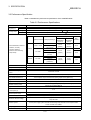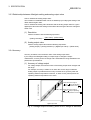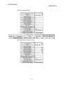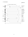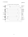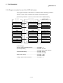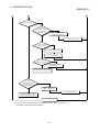
1
Digital-Analog Converter Module type AJ65SBT-62DA , User s Manual Mitsubishi Programmable Logic Controller SAFETY PRECAUTIONS (Always read these precautions before using this equipment.) Before using this product, please read this manual and the relevant manuals introduced in this manual carefully and pay full attention to safety to handle the product correctly. The precautions given in this manual are concerned with this product. Refer to the user's manual of the CPU module to use for a description of the PLC system safety precautions. In this manual, the safety instructions are ranked as "DANGER" and "CAUTION". DANGER Indicates that incorrect handling may cause hazardous conditions, resulting in death or severe injury. ! CAUTION Indicates that incorrect handling may cause hazardous conditions, resulting in medium or slight personal injury or physical damage. ! Note that the ! CAUTION level may lead to a serious consequence according to the circumstances. Always follow the precautions of both levels because they are important to personal safety. Please save this manual to make it accessible when required and always forward it to the end user. [Design Precautions] ! DANGER Configure a safety circuit so that the safety of the overall system is maintained even when an external power error of PLC error occurs. Accident may occur due to output error or malfunctioning. (1) The status of analog output changes depending on the setting of various functions that control the analog output. Take sufficient caution when setting for those functions. For details of analog output status, refer to Section 3.4.1 "Combinations of functions in each part" (2) Normal output may not be obtained due to malfunctions of output elements or the internal circuits. Configure a circuit to monitor signals which may lead to a serious accident. ! CAUTION Do not bunch the control wires or communication cables with the main circuit or power wires, or install them close to each other. They should be installed 100mm (3.9inch) or more from each other. Not doing so could result in noise that would cause erroneous operation. A-1 [Installation Precautions] ! CAUTION Use the PLC in the environment that meets the general specifications contained in this Manual. Using the PLC outside the range of the general specifications may result in electric shock, fire or malfunction, or may damage or degrade the module. Securely fix the module to a DIN rail or with mounting screws, and securely tighten the mounting screws within the specified torque range. Undertightening can cause a drop or malfunction. Overtightening can cause a drop or malfunction due to damage of the screws or module. Do not touch the conducted area or electric parts of the module. Doing so may cause module malfunction or breakdowns. [Wiring Precautions] ! CAUTION Always switch power off externally in all phases before starting installation, wiring and other works. Not doing so can cause the product to be damaged or malfunction. Always earth the FG terminal to the protective earth conductor. Not doing so can cause a malfunction. Wire the module correctly after confirming the rated voltage and terminal layout of the product. Not doing so can cause a fire or failure. Tighten the terminal screws within the specified torque range. Undertightening can cause a short circuit or malfunction. Overtightening can cause a short circuit or malfunction due to damage of the screws or module. Ensure that no foreign matter such as chips and wire-offcuts enter the module. Foreign matter can cause a fire, failure or malfunction. A-2 [Wiring Precautions] ! CAUTION When connecting the communication and power supply cables to the module, always run them in conduits or clamp them. Not doing so can damage the module and cables due to loose, moved or accidentally pulled cables or can cause a malfunction due to a cable connection fault. When disconnecting the communication and power supply cables from the module, do not hold and pull the cable part. Disconnect the cables after loosening the screws in the portions connected to the module. Pulling the cables connected to the module can damage the module and cables or can cause a malfunction due to a cable connection fault. [Starting and Maintenance Precautions] ! CAUTION Do not touch the terminals while the power is on. Doing so may cause malfunction. Always start cleaning or terminal screw retightening after switching power off externally in all phases. Not doing so can cause the module to fail or malfunction. Undertightening can cause a drop, short circuit or malfunction. Overtightening can cause a drop, short circuit or malfunction due to damage of the screws or module. Never disassemble or modify the module. This may cause breakdowns, malfunction, injury and/or fire. Do not drop the module or give it hard impact since its case is made of resin. Doing so can damage the module. Mount or dismount the module to or from an enclosure after switching power off externally in all phases. Not doing so can cause the module to fail or malfunction. [Disposal Precautions] ! CAUTION When disposing of this product, treat it as industrial waste. A-3 REVISIONS * The manual number is given on the bottom left of the back cover. Print Date * Manual Number Oct., 2000 SH (NA) 080107-A First printing Revision Japanese Manual Version SH-080088-A This manual confers no industrial property rights or any rights of any other kind, nor does it confer any patent licenses. Mitsubishi Electric Corporation cannot be held responsible for any problems involving industrial property rights which may occur as a result of using the contents noted in this manual. 2000 MITSUBISHI ELECTRIC CORPORATION A-4 INTRODUCTION Thank you for choosing the Mitsubishi MELSEC-A series general-purpose programmable controller. Before using the product, please read this manual carefully to use it to its optimum. CONTENTS SAFETY PRECAUTIONS..............................................................................................................................AREVISIONS ....................................................................................................................................................AAbout Manuals ...............................................................................................................................................AConformation to the EMC Directive and Low Voltage Instruction ................................................................AAbout the Generic Terms and Abbreviations ................................................................................................AProduct Components .....................................................................................................................................A1. OVERVIEW 1 4 7 7 8 9 1- 1 to 1- 2 1.1 Features ................................................................................................................................................... 1- 1 2. SYSTEM CONFIGURATION 2- 1 to 2- 2 2.1 Overall Configuration ............................................................................................................................... 2- 1 2.2 Applicable System.................................................................................................................................... 2- 2 3 SPECIFICATION 3- 1 to 3- 16 3.1 General Specification............................................................................................................................... 3- 1 3.2 Performance Specification....................................................................................................................... 3- 2 3.3 I/O Conversion Characteristics................................................................................................................ 3- 3 3.3.1 Voltage output characteristics........................................................................................................... 3- 4 3.3.2 Current output characteristics ........................................................................................................... 3- 5 3.3.3 Relationship between offset/gain setting and analog output value ................................................. 3- 6 3.3.4 Accuracy............................................................................................................................................ 3- 6 3.3.5 Conversion speed ............................................................................................................................. 3- 7 3.4 Function.................................................................................................................................................... 3- 8 3.4.1 Combinations of various functions.................................................................................................... 3- 9 3.5 Remote I/O Signals ................................................................................................................................. 3- 10 3.5.1 Remote I/O signal list ....................................................................................................................... 3- 10 3.5.2 Functions of the remote I/O signals................................................................................................. 3- 11 3.6 Remote Register ..................................................................................................................................... 3- 13 3.6.1 Allocation of the remote register ...................................................................................................... 3- 13 3.6.2 CH. digital value setting (Addresses RWwm, RWwm+1) ......................................................... 3- 14 3.6.3 Analog output enable/disable setting (Address RWwm+2) ............................................................ 3- 14 3.6.4 Output range/HOLD/CLEAR setting (Address RWwm+3) ............................................................. 3- 15 3.6.5 CH. check code (Addresses RWrn, RWrn+1) ............................................................................ 3- 16 3.6.6 Error code (Address RWrn+2) ......................................................................................................... 3- 16 4 SETUP AND PREPARATION BEFORE OPERATION 4- 1 to 4- 10 4.1 Pre-Operation Procedure......................................................................................................................... 4- 1 A-5 4.2 Precautions When Handling .................................................................................................................... 44.3 Name of Each Part................................................................................................................................... 44.4 Offset/Gain Setting................................................................................................................................... 44.5 Section Number Setting........................................................................................................................... 44.6 Facing Direction of the Module Installation ............................................................................................. 44.7 Data Link Cable Wiring ............................................................................................................................ 44.7.1 Instructions for handling the CC-Link dedicated cables................................................................... 44.7.2 Connection of the CC-Link dedicated cables ................................................................................... 44.8 Wiring........................................................................................................................................................ 44.8.1 Wiring precautions............................................................................................................................. 44.8.2 Wiring of module with external equipment ....................................................................................... 44.9 Maintenance and Inspection.................................................................................................................... 45 PROGRAMMING 1 3 5 7 7 8 8 8 8 8 9 9 5- 1 to 5- 20 5.1 Programming Procedure.......................................................................................................................... 5- 1 5.2 Program Examples .................................................................................................................................. 5- 2 5.2.1 Program examples for use of the ACPU/QCPU (A mode) (FROM/TO instructions)...................... 5- 2 5.2.2 Program examples for use of the ACPU/QCPU (A mode) (dedicated instructions)....................... 5- 7 5.2.3 Program examples for use of the QnACPU .................................................................................... 5- 12 5.2.4 Program examples for use of the QCPU (Q mode) ........................................................................ 5- 16 6 TROUBLESHOOTING 6- 1 to 6- 6 6.1 Error Code List ......................................................................................................................................... 6- 1 6.2 Using the LED Indications to Check Errors............................................................................................. 6- 2 6.3 Troubleshooting for the Case where the “ERR.” LED of the Master Station Flickers ........................... 6- 4 APPENDIX Appendix- 1 to Appendix- 4 Appendix1 Comparison between This Product and Conventional Product ....................................Appendix- 1 Appendix2 External dimension diagram...........................................................................................Appendix- 3 A-6 About Manuals The following manuals are also related to this product. In necessary, order them by quoting the details in the tables below. Related Manuals Manual Number Manual Name (Model Code) CC-Link System Master/Local Module User's Manual type AJ61BT11/A1SJ61BT11 Describes the system configuration, performance specifications, functions, handling, wiring and troubleshooting of the AJ61BT11 and A1SJ61BT11. (Optionally available) IB-66721 (13J872) CC-Link System Master/Local Module User's Manual type AJ61QBT11/A1SJ61QBT11 Describes the system configuration, performance specifications, functions, handling, wiring and troubleshooting of the AJ61QBT11 and A1SJ61QBT11. (Optionally available) IB-66722 (13J873) CC-Link System Master/Local Module User's Manual type QJ61BT11 Describes the system configuration, performance specifications, functions, handling, wiring and troubleshooting of the QJ61BT11. (Optionally available) type AnSHCPU/AnACPU/AnUCPU/QCPU-A (A mode) Programming Manual (Dedicated Instructions) Explains the instructions extended for the AnSHCPU/AnACPU/AnUCPU/ QCPU-A (A mode). IB-080016 (13JL91) IB-66251 (13J742) (Optionally available) Conformation to the EMC Directive and Low Voltage Instruction When complying with EMC Directives and Low-Voltage Directives by assembling a Mitsubishi PLC compatible with EMC Directive and Low-Voltage Directives into the user product, refer to Chapter 3 "EMC Directives and Low-Voltage Directives" in the User's Manual (Hardware) for the CPU module being used. The CE logo is printed on the rating plate on the main body of the PLC that conforms to the EMC directive and low voltage instruction. A-7 About the Generic Terms and Abbreviations Unless otherwise specified, the following generic terms and abbreviations are used in this manual to describe Type AJ65SBT-62DA digital-analog conrerter module. Generic Term/Abbreviation GPPW ACPU QnACPU QCPU (A mode) QCPU (Q mode) Master station Local station Remote I/O station Remote device station Remote station Intelligent device station Master module SB SW RX RY RWw RWr Description Abbreviation for the SW4D5C-GPPW-E or later GPP function software. Generic term for A0J2CPU, A0J2HCPU, A1CPU, A2CPU, A2CPU-S1, A3CPU, A1SCPU, A1SCPU-S1, A1SCPUC-24-R2, A1SHCPU, A1SJCPU, A1SJCPU-S3, A1SJHCPU, A1NCPU, A2NCPU, A2NCPU-S1, A3NCPU, A3MCPU, A3HCPU, A2SCPU, A2SCPU-S1, A2SHCPU, A2ACPU, A2ACPU-S1, A3ACPU, A2UCPU, A2UCPU-S1, A2ASCPU, A2ASCPU-S1, A2ASCPU-S30, A2USHCPU-S1, A3UCPU, A4UCPU Generic term for Q2ACPU, Q2ACPU-S1, Q2ASCPU, Q2ASCPU-S1, Q2ASHCPU, Q2ASHCPU-S1, Q3ACPU, Q4ACPU, Q4ARCPU Generic term for Q02CPU-A, Q02HCPU-A, Q06HCPU-A Generic term for Q02CPU, Q02HCPU, Q06HCPU, Q12HCPU, Q25HCPU Station that controls the data link system. One master station is required for each system. Station having a PLC CPU and the ability to communicate with the master and other local stations. Remote station that handles bit unit data only. (Performs input and output with external devices.) (AJ65BTB1-16D, AJ65SBTB1-16D) Remote station that handles bit unit and word unit data only. (Performs input and output with external devices, and analog data exchange.) Generic term for remote I/O station and remote device station. (Controlled by the master station) Station that can perform transient transmission, such as the AJ65BT-R2 (including local stations). Generic term for QJ61BT11, AJ61BT11, A1SJ61BT11, AJ61QBT11, and A1SJ61QBT11 when they are used as master stations. Link special relay (for CC-Link) Bit unit information that indicates the module operating status and data link status of the master station/local station. (Expressed as SB for convenience) Link special register (for CC-Link) 16 bit unit information that indicates the module operating status and data link status of the master station/local station. (Expressed as SW for convenience) Remote input (for CC-Link) Information entered in bit units from the remote station to the master station. (Expressed as RX for convenience) Remote output (for CC-Link) Information output in bit units from the remote station to the master station. (Expressed as RY for convenience) Remote register (Write area for CC-Link) Information output in 16-bit units from the master station to the remote device station. (Expressed as RWw for convenience) Remote register (Read area for CC-Link) Information entered in 16-bit units from the master station to the remote device station. (Expressed as RWr for convenience) A-8 Product Components This product consists of the following. Product Name Type AJ65SBT-62DA digital - analog converter module Type AJ65SBT-62DA digital - analog converter module user's manual (hardware) A-9 Quantity 1 1 MEMO A - 10 1 OVERVIEW MELSEC-A 1 OVERVIEW 1 This user's manual explains the specifications, handling, programming methods and others of Type AJ65SBT-62DA digital-analog converter module (hereafter abbreviated to the "AJ65SBT-62DA") which is used as a remote device station of a Control & Communication Link (hereafter abbreviated to "CC-Link") system. The AJ65SBT-62DA is a module designed to convert digital values (16-bit signed BIN data) from outside the PLC into analog values (voltages or currents). 1.1 Features This section gives the features of the AJ65SBT-62DA. (1) High accuracy This module performs D/A conversion at the accuracy of ±0.4% relative to the maximum value of the analog output value at the operating ambient temperature of 0 to 55°C, or at ±0.2% relative to the maximum value of the analog output value at the operating ambient temperature of 25±5°C. (2) Output range selectable per channel You can choose the analog output range per channel to change the I/O conversion characteristics. (3) High resolution of 1/±4000 By changing the output range, you can choose and set the resolution to either 1/4000 or 1/±4000 (when the -10 to +10V range or user range setting 1 is selected) to provide high-resolution analog values. (4) Setting of analog output hold or clear at STOP of PLC CPU You can specify whether to hold or clear the analog value which is being output from each channel of the unit when the PLC CPU has entered the STOP mode or the AJ65SBT-62DA has stopped D/A conversion due to error occurrence. (5) Smaller than the conventional D/A converter module This module is 60% smaller in installation area and 38% less in volume than the conventional CC-Link D/A converter module (AJ65BT-64DAV/DAI). (6) Up to 42 modules connectable You can connect up to 42 AJ65SBT-62DA modules to one master station. 1-1 1 OVERVIEW MELSEC-A MEMO 1-2 2 SYSTEM CONFIGURATION MELSEC-A 2 SYSTEM CONFIGURATION This chapter describes the system configuration for use of the AJ65SBT-62DA. 2.1 Overall Configuration 2 The overall configuration for use of the AJ65SBT-62DA is shown below. CC-Link master/local module (master station) (AJ61BT11, A1SJ61BT11, AJ61QBT11, A1SJ61QBT11, QJ61BT11) CC-Link master/local module (local station) (AJ61BT11, A1SJ61BT11, AJ61QBT11, A1SJ61QBT11, QJ61BT11) Terminal resistor CC-Link dedicated cable (Intelligent device station) (Remote I/O station) Terminal resistor AJ65SBT-62DA (Remote device station) (Remote device station) 1 station occupied RX/RY: 32 points each RWr/RWw: 4 points each Object to which voltage/current will be output 2-1 2 SYSTEM CONFIGURATION MELSEC-A 2.2 Applicable System This section explains the applicable system. (1) Applicable master modules The following master modules can be used with the AJ65SBT-62DA. AJ61BT11 A1SJ61BT11 AJ61QBT11 A1SJ61QBT11 QJ61BT11 (2) Restrictions on use of CC-Link dedicated instructions The CC-Link dedicated instructions may not be used depending on the PLC CPU or master module used For details of the restrictions, refer to the A series master module user's manual. 2-2 3 SPECIFICATION MELSEC-A 3 SPECIFICATION This chapter provides the specifications of the AJ65SBT-62DA. 3.1 General Specification Table 3.1 indicates the general specifications of the AJ65SBT-62DA. Table 3.1 General specification Item 3 Specification Usage ambient temperature 0 to 55°C Storage ambient temperature -20 to 75°C Usage ambient humidity 10 to 90%RH, no condensation Storage ambient humidity 10 to 90%RH, no condensation When there is intermittent vibration Conforming to JIS B 3501, IEC 1131-2 Vibration durability Shock durability Frequency Acceleration Amplitude 10 to 57Hz — 0.075mm (0.0030inch) 57 to 150Hz 9.8m/s2 — When there is continuous vibration Frequency Acceleration Amplitude 10 to 57Hz — 0.035mm (0.0013inch) 57 to 150Hz 4.9m/s2 — Sweep count 10 times in each direction X, Y, Z (80 minutes) Conforming to JIS B 3501, IEC1131-2 (147m/s2, 3 times each in 3 directions) Usage environment Usage height No corrosive gas Less than 2000 m (less than 6562 ft.) Installation area Within the control board Over-voltage category *1 Less than II 2 Pollution level * Less than 2 *1 Indicates the location where the device is connected from the public cable network to the device structure wiring area. Category II applies to the devices to which the power is supplied from a fixed equipment. Surge withstand voltage for devices with up to 300V of rated voltage is 2500V. *2 This is an index which indicates the degree of conductive object generation in the environment Pollution level 2 is when only non-conductive pollution occurs. A temporary conductivity caused by condensation must be expected occasionally. 3-1 3 SPECIFICATION MELSEC-A 3.2 Performance Specification Table 3.2 indicates the performance specifications of the AJ65SBT-62DA. Table 3.2 Performance Specifications Item Digital input Analog output AJ65SBT-62DA Voltage 16-bit signed binary (-4096 to +4095) Current 16-bit signed binary (0 to 4095) Voltage -10 to +10VDC (external load resistance: 2k Current to 1M 0 to 20mADC (external load resistance: 0 to 600 ) ) Accuracy Digital Input Value Analog Input Range -4000 to +4000 User range setting 1 (-10 to +10V) Ambient temperature 0 to 55°C Ambient temperature 25±5°C ±0.4% (±40mV) ±0.2% (±20mV) ±0.4% (±20mV) ±0.2% (±10mV) ±0.4% (±80µA) ±0.2% (±40µA) -10 to +10V I/O characteristics, maximum resolution, accuracy (accuracy relative to maximum value of analog output value) Voltage Max. Resolution 0 to 5V 0 to 4000 1.25mV 1 to 5V User range setting 2 (0 to 5V) 0 to 20mA Current 1.0mV 5µA 4 to 20mA 0 to 4000 2.5mV User range setting 3 (0 to 20mA) 4µA Factory setting is -10 to +10V. Maximum conversion speed 1ms/1 channel Output short-circuit protection Yes Absolute maximum output Voltage: ±12V, Current +21mA Number of analog output points 2 channels/1 module Number of occupied stations Connected terminal block 1 station (RX/RY: 32 points each, RWr/RWw: 4 points each) 7-point, 2-piece terminal block (transmission, power supply) Direct-coupled, 18-point terminal block (analog output section) (M3 screw) 0.3 to 0.75mm2 Applicable wire size Applicable crimping terminal Module mounting screw Applicable DIN rail RAV1.25-3.5 (conforming to JIS C2805) M4 screw × 0.7mm × 16mm or more (tightening torque range: 78 to 108N cm) Can also be mounted to DIN rail TH35-7.5Fe, TH35-7.5Al (conforming to JIS-C2B12) 24VDC internal current consumption (A) External power supply Noise immunity Dielectric withstand voltage Isolation system 0.16 DC24V (DC20.4V to DC26.4V) Inrush current: 8.2A, within 2.1ms By noise simulator of 500Vp-p noise voltage, 1µs noise width and 25 to 60Hz noise frequency 500VAC for 1 minute across all power supply and communication system terminals and all analog output terminals Across communication system terminals and all analog output terminals: Photocoupler isolated Across power supply system terminals and all analog output terminals: Photocoupler isolated Across channels: Non-isolated Weight (kg) 0.20 Outline dimensions (mm) 118 (W) × 50 (H) × 40 (D) 3-2 3 SPECIFICATION MELSEC-A 3.3 I/O Conversion Characteristics An I/O conversion characteristic indicates an inclination of a straight line which connects an offset value and a gain value at the time when a digital value set from the PLC CPU is converted into an analog value (voltage or current output). The offset value is an analog value (voltage or current) output when the digital value set from the PLC CPU is 0. The gain value is an analog value (voltage or current) output when the digital value set from the PLC CPU is 4000. 3-3 3 SPECIFICATION MELSEC-A 3.3.1 Voltage output characteristics The voltage output characteristic graph is shown below. 1 5 Practical analog output scope Analog output voltage (V) 10 3 1 2 0 -5 -10 -4096 -4000 -2000 0 2000 4000 4095 Digital input value Number Analog Output Range Setting Offset Value Gain Value Digital Input Value Maximum Resolution 1) -10 to +10v 0V 10V -4000 to +4000 2.5mV 2) 0 to 5V 0V 5V 3) 1 to 5V 1V 5V — User range setting 1 (-10 to +10v) 0V 10V -4000 to +4000 2.5mV — User range setting 2 (0 to 5v) 0V 5V 0 to 4000 1.0mV 0 to 4000 1.25mV 1.0mV Fig. 3.1 Voltage Output Characteristic POINT (1) Within the digital input and analog output scopes of each output range, the maximum resolution and accuracy are within the performance specification range. Outside those scopes, however, they may not fall within the performance specification range. (Avoid using the dotted line part in Fig. 3.1.) (2) Set the offset and gain values of the user range setting within the range satisfying the following conditions. (a) Setting range when user range setting 1 is selected: -10 to +10V (b) Setting range when user range setting 2 is selected: 0 to 5V (c) (Gain value) > (Offset value) If you attempt to make setting outside the setting range of (a) or (b), the "RUN" LED flickers at 0.5s intervals. Set the values within the setting range. If you attempt to make setting outside the setting range of (c), the "RUN" LED flickers at 0.5s intervals. Make setting again. 3-4 3 SPECIFICATION MELSEC-A 3.3.2 Current output characteristics The current output characteristic graph is shown below. Practical analog output scope Analog output voltage (mA) 20 15 10 2 1 5 4 0 0 2000 4000 4095 Digital input value Number Analog Output Range Setting Offset Value Gain Value 1) 0 to 20mA 0mA 20mA 2) 4 to 20mA 4mA 20mA — User range setting 3 (0 to 20mA) 0mA 20mA Digital Input Value Maximum Resolution 5µA 0 to 4000 4µA Fig. 3.2 Current Output Characteristic POINT (1) Within the digital input and analog output scopes of each output range, the maximum resolution and accuracy are within the performance specification range. Outside those scopes, however, they may not fall within the performance specification range. (Avoid using the dotted line part in Fig. 3.2.) (2) Set the offset and gain values of the user range setting within the range satisfying the following conditions. (a) Setting range when user range setting 3 is selected: 0 to 20mA (b) (Gain value) > (Offset value) If you attempt to make setting outside the setting range of (a), the "RUN" LED flickers at 0.5s intervals. Set the values within the setting range. If you attempt to make setting outside the setting range of (b), the "RUN" LED flickers at 0.5s intervals. Make setting again. 3-5 3 SPECIFICATION MELSEC-A 3.3.3 Relationship between offset/gain setting and analog output value How to calculate the analog output value: The resolution of AJ65SBT-62DA can be set arbitrarily by modifying the setting of the offset value and gain value. How to calculate the analog value resolution and the analog output value for a given digital input value when the settings of the offset value and gain value are changed is shown next. (1) Resolution Find the resolution with the following expression. (Gain value) - (Offset value) 4000 (Analog resolution) = (2) Analog output value Find the analog output value with the following expression. (Analog output) = (Analog resolution) × (Digital input value) + (Offset value) 3.3.4 Accuracy Accuracy is relative to the maximum value of the analog output value. If you change the offset/gain setting or output range to change the output characteristic, accuracy does not change and is held within the range indicated in the performance specifications. (1) Accuracy of voltage output For voltage output, the maximum value of the analog output value changes with the range. For example, accuracy is relative to 5V when the 0 to 5V range is selected. Analog output is provided at the accuracy of within ±0.2% (±10mV) when the operating ambient temperature is 25±5°C, or within ±0.4% (±20mA) when the operating ambient temperature is 0 to 55°C. 5V Analog output voltage Varies within the range of 0.2% ( 10mV) at operating ambient temperature of 25 5 . Varies within the range of 0.4% ( 20mV) at operating ambient temperature of 0 to 55 . 0V 0 4000 Digital input value Fig. 3.3 Voltage Output Accuracy (When 0 to 5V Range Is Selected) 3-6 3 SPECIFICATION MELSEC-A (2) Accuracy of current output For current output, accuracy is relative to 20mA. Analog output is provided at the accuracy of within ±0.2% (±40µA) when the operating ambient temperature is 25±5°C, or within ±0.4% (±80µA) when the operating ambient temperature is 0 to 55°C. 20mA Analog output value Varies within the range of 0.2% ( 40 A) at operating ambient temperature of 25 5 . Varies within the range of 0.4% ( 80 A) at operating ambient temperature of 0 to 55 . 0mA 0 4000 Digital input value Fig. 3.4 Current Output Accuracy 3.3.5 Conversion speed Conversion speed indicates time required to read the digital output value written to the buffer memory, perform D/A conversion, and then output the specified analog value. Conversion speed per channel of the AJ65SBT-62DA is 1ms. Due to the data link processing time of the CC-Link system, there is a transmission delay until the D/A conversion value is read actually. For the data link processing time, refer to the user's manual of the master module used. Example) Data link processing time taken when the master module is the AJ61BT11 or A1SJ61BT11 [Calculation expression] SM+LS×2+remote device station processing time SM: Scan time of master station sequence program LS : Link scan time Remote device station processing time: (Number of channels used+1*) × 1ms *: Internal processing time of AJ65SBT-62DA 3-7 3 SPECIFICATION MELSEC-A 3.4 Function Table 3.3 lists the functions of the AJ65SBT-62DA. Table 3.3 AJ65SBT-62DA Function List Item Description Refer to D/A output enable/disable function Specify whether the D/A conversion value is output or the offset value is output per channel. Note that the conversion speed is constant independently of the output enable/disable setting. Section 3.5.2 D/A conversion enable/disable function Specify whether D/A conversion is enabled or disabled per channel. The sampling cycle can be shortened by setting the unused channel to D/A conversion disable. Section 3.6.3 You can set the analog output range per channel to change the I/O conversion characteristics. Select the output range setting from among the following 8 types. Output range changing function Output Range Set Value -10 to +10V 0H 0 to 5V 1H 1 to 5V 2H 0 to 20mA 3H 4 to 20mA 4H User range setting 1 (-10 to +10V) 5H User range setting 2 (0 to 5V) 6H User range setting 3 (0 to 20mA) 7H Section 3.6.4 Function to specify hold or clear of the analog output when the PLC CPU is in the STOP status (HOLD/CLEAR setting) Specify per channel whether to hold or clear (output the offset value) the analog value which is being output from each channel when the PLC CPU has entered the STOP status or the AJ65SBT-62DA has stopped D/A conversion due to error occurrence. Section 3.6.4 Offset/gain setting You can make offset/gain setting per channel without potentiometers to change the I/O conversion characteristics freely. Section 4.4 3-8 3 SPECIFICATION MELSEC-A 3.4.1 Combinations of various functions You can set the analog output as indicated in Table 3.4 by combining the HOLD/CLEAR setting, CH. analog output enable/disable flag and Analog output enable/disable setting. Make setting according to your system application. Table 3.4 Analog output status combination list Setting combination Execution status Analog output enable/disable setting Enable (1) CH. analog output enable/disable flag HOLD/CLEAR setting Enable (ON) Enable or disable HOLD or CLEAR HOLD or CLEAR Output of the analog value after D/A conversion from the digital value specified by the PLC CPU Offset value 0V/0mA Analog output status when the PLC CPU is in the STOP status Analog value before the PLC CPU stop is retained Offset value Offset value 0V/0mA Analog output status at PLC CPU stop error Analog value before the PLC CPU stop is retained Offset value Offset value 0V/0mA Offset value 0V/0mA Offset value 0V/0mA Analog output status when the "L RUN" LED turns off/"L.ERR" LED turns on CLEAR Prohibit (OFF) Analog output status when the PLC CPU is in the RUN status Analog output status at occurrence of AJ65SBT-62DA digital value setting error HOLD Prohibit (0) Output of the maximum or minimum analog value The analog value before the "L RUN" LED turns off is retained. Offset value Analog output status when the "L ERR." LED flickers Output of the analog value after D/A conversion from the digital value specified by the PLC CPU Offset value 0V/0mA Analog output status in initial processing completion status after power-reset Output of the analog value after D/A conversion from the digital value specified by the PLC CPU Offset value 0V/0mA Analog output status at occurrence of AJ65SBT-62DA output range setting error 0V/0mA 0V/0mA 0V/0mA 0V/0mA Analog output status at occurrence of AJ65SBT-62DA watchdog timer error 0V/0mA 0V/0mA 0V/0mA 0V/0mA 3-9 3 SPECIFICATION MELSEC-A 3.5 Remote I/O Signals This section describes the assignment and functions of the remote I/O signals. 3.5.1 Remote I/O signal list Remote inputs (RX) mean the input signals from the AJ65SBT-62DA to the master module, and remote outputs (RY) mean the output signals from the master module to the AJ65SBT-62DA. In communications with the master station, the AJ65SBT-62DA uses 32 points of the remote inputs (RX) and 32 points of the remote outputs (RY). Table 3.5 indicates the assignment and names of the remote I/O signals. Table 3.5 Remote I/O Signals List Signal Direction: AJ65SBT-62DA Master Module Remote input (RX) Name RXn0 to RXnB Reserved RXnC E PROM write error flag RXnD RXnE RXnF Signal Direction: Master Module AJ65SBT-62DA Remote output (RY) Name RYn0 CH.1 analog output enable/disable flag 2 Reserved Test mode flag RYn1 CH.2 analog output enable/disable flag RX (n+1) 0 to RX (n+1) 7 Reserved RYn2 to RY (n+1) 7 Reserved RX (n+1) 8 Initial data processing request flag RY (n+1) 8 Initial data processing complete flag RX (n+1) 9 Initial data setting complete flag RY (n+1) 9 Initial data setting request flag RX (n+1) A Error status flag RY (n+1) A Error reset request flag RX (n+1) B Remote READY RX (n+1) C to RX (n+1) F Reserved RY (n+1) B to RY (n+1) F Reserved POINT The reserved devices given in Table 3.5 are used by the system and cannot be used by the user. If the user has used (turned on/off) any of them, we cannot guarantee the functions of the AJ65SBT-62DA. 3 - 10 3 SPECIFICATION MELSEC-A 3.5.2 Functions of the remote I/O signals Table 3.6 explains the functions of the remote I/O signals of the AJ65SBT-62DA. Table 3.6 Remote I/O Signal Details (1/2) Device No. Signal Name Description 2 Turns on the number of E PROM write times exceeds its limit (1000,000 times per 2 RXnC E PROM write error flag RXnF Test mode flag channel). If this flag has turned on, this module itself has failed (hardware fault) and therefore this flag cannot be reset (turned off) by the error reset request flag. Turns on in the test mode. (Used for interlock to prevent wrong output during offset/gain setting.) After power-on, the initial data processing request flag is turned on by the AJ65SBT-62DA to request the initial data to be set. Also, after the initial data processing is complete (initial data processing complete flag RY (n+1) 8 ON), the flag is turned off. RX(n+1)8 Initial data processing request flag RY(n+1)8 Initial data processing complete flag RX (n+1) 8 Initial data processing request flag RX(n+1)9 Initial data setting complete flag RY(n+1)9 Initial data setting request flag RX(n+1)B Remote ready : Performed by sequence ladder : Performed by AJ65SBT-62DA RX (n+1) 9 Initial data setting complete flag When the initial data setting request (RY (n+1) 9 ON) is made, the flag turns on after the initial data setting completion is done. Also, after the initial data setting is complete, the initial setting complete flag turns off when the initial data setting request flag turns off. Turns on at occurrence of the output range setting error, digital value setting error 2 or E PROM write error (RXnC). Does not turn on at occurrence of the watchdog timer error. (The "RUN" LED goes off.) RX(n+1)A Error status flag RY(n+1)A Error reset request flag RX (n+1) A Error status flag RWrn+2 Error code 0 Error code 0 RWrn, RWrn+1 CH. check code 0 Check code 0 : Performed by sequence ladder : Performed by AJ65SBT-62DA RX (n+1) B Remote READY Turns on when initial data setting is completed after power-on or at termination of the test mode. (Used for interlocking read/write from/to the master module.) n: Address allocated to the master module by station number setting. 3 - 11 3 SPECIFICATION MELSEC-A Table 3.6 Remote I/O Signal Details (2/2) Device No. Signal Name Description CH. analog output enable/disable flag D/A conversion value output enable flag for channel 1 or 2. Turn on this flag to enable the D/A conversion value of the corresponding channel to be output. Turn off when you want to disable the output of the D/A conversion value. Processed on the leading edge of ON/OFF. RY (n+1) 8 Initial data processing complete flag Turns on after initial data processing completion when initial data processing is requested after power-on or test mode operation. RY (n+1) 9 Initial data setting request flag RYn0 to RYn1 RY (n+1) A Error reset request flag Turns on at the time of initial data setting or changing. Turning on this flag resets (turns off) the error status flag (RX(n+1)A) and also check code (RWrn, clears (to 0000H) the error code (RWrn+2) and CH. 2 RWrn+1) in the remote register. However, since the E PROM write error flag (RXnC) cannot be reset, the error status flag remains on, too. n: Address allocated to the master module by station number setting. 3 - 12 3 SPECIFICATION MELSEC-A 3.6 Remote Register The AJ65SBT-62DA has a remote resister for data communication with the master module. The remote register allocation and data structures are described below. 3.6.1 Allocation of the remote register The allocation of the remote register is shown in Table 3.7. Table 3.7 Allocation of the remote register Transfer Direction Master Remote Remote Master Address Description Default Value RWwm CH. 1 digital value setting 0 Refer to RWwm+1 CH. 2 digital value setting 0 RWwm+2 Analog output enable/disable setting 0 Section 3.6.3 RWwm+3 Output range/HOLD/CLEAR setting 0 Section 3.6.4 RWrn CH. 1 check code 0 RWrn+1 CH. 2 check code 0 RWrn+2 Error code 0 RWrn+3 Reserved 0 Section 3.6.2 Section 3.6.5 Section 3.6.6 m, n: The address set for the master station in the station number setting. POINT Do not execute read or write to the remote register that is not allowed to use. When a read or write is executed, the functions of the AJ65SBT-62DA is not guaranteed. 3 - 13 3 SPECIFICATION 3.6.2 CH. MELSEC-A digital value setting (Addresses RWwm, RWwm+1) (1) This area is used to write the digital value for the D/A conversion from the PLC CPU. (2) The digital value at all channels become “0” in the following conditions: (a) After the power is turned on, when the remote READY (RX(n+1)B) is turned on. (3) The digital value that may be set is a 16-bit signed binary within the setting range which matches the output range setting. If a value beyond the range of the digital value resolution is set, the data in Table 3.8 is applied for the D/A conversion. In addition, the checking code is stored in the check code storage area (addresses RWrn, RWrn+1). Table 3.8 Available setting range of the digital value Output Range Available setting range Digital value for the D/A conversion when the value beyond the range is set -10 to +10V User range setting 1 -4096 to +4095 (Practical scope: -4000 to +4000) 4096 or more: 4095 -4097 or less: -4096 0 to 5V 1 to 5V User range setting 2 0 to 20mA 4 to 20mA User range setting 3 -96 to 4095 (Practical scope: 0 to 4000) 4096 or more: 4095 -97 or less: -96 3.6.3 Analog output enable/disable setting (Address RWwm+2) (1) Set whether D/A conversion is enabled or disabled per channel. (2) The default setting is conversion disable for all channels. b15 b14 b13 b12 b11 b10 b9 b8 b7 b6 b5 b4 b3 b2 b1 b0 CH.2 CH.1 Ignored 3 - 14 0: Conversion disable 1: Conversion enable 3 SPECIFICATION MELSEC-A 3.6.4 Output range/HOLD/CLEAR setting (Address RWwm+3) (1) Make output range setting using the 8 upper bits (b8 to b15) of address RWwm+3. Make HOLD/CLEAR setting using the 8 lower bits (b0 to b7) of address RWwm+3. (2) The default settings are -10 to +10V and CLEAR. b15 to b12 b11 b8 to CH.2 b7 b4 to CH.1 b3 to CH.2 Output range setting b0 CH.1 HOLD/CLEAR setting : CLEAR 0H 1 to FH: HOLD 0H: -10 to +10V 1H: 0 to 5V 2H: 1 to 5V 3H: 0 to 20mA 4H: 4 to 20mA 5H: User range setting 1 (-10 to +10V) 6H: User range setting 2 (0 to 5V) 7H: User range setting 3 (0 to 20mA) Example Set 5101H when setting channel 1 to "0 to 5V" and "HOLD" and channel 2 to "User range setting 1" and "CLEAR". b15 b14 b13 b12 b11 b10 0 1 0 1 0 0 b9 0 b8 1 b7 0 b6 0 b5 0 b4 0 b3 0 b2 0 b1 0 CH.2 CH.1 CH.2 CH.1 5 1 0 1 3 - 15 b0 1 5101H 3 SPECIFICATION 3.6.5 CH. MELSEC-A check code (Addresses RWrn, RWrn+1) (1) This area is used to check if the digital value is within or out of the setting range. One of the following checking codes is stored when the digital value lower or higher than the setting range is set. Check code Description 000FH A digital value which exceeds the setting range was set. 00F0H A digital value which is below the setting range was set. 00FFH The digital value less than the setting range and the digital value more than the setting range were set before the error reset request. (2) The check code once stored is not reset even if the set value is set to within the valid setting allowed range. (3) The storage area or the check code is reset by turning on the error reset request flag (RY (n+1)A). 3.6.6 Error code (Address RWrn+2) If an error occurs (the RUN LED flickers) when data is written to the AJ65SBT-62DA, the corresponding error code is stored into the remote register (address RWrn+2) of the AJ65SBT-62DA. Refer to Section 6.1 for details of the error codes. 3 - 16 4 SETUP AND PREPARATION BEFORE OPERATION MELSEC-A 4 SETUP AND PREPARATION BEFORE OPERATION 4.1 Pre-Operation Procedure This section explains the preparatory procedure for operating the AJ65SBT-62DA. START Create a program. (When making offset/gain setting, set all channels to any of user range settings 1 to 3 in the sequence program.) .......Refer to Chapter 5. 4 No Make offset/gain setting? Yes Start data link. Offset/gain setting (Refer to Section 4.4.) END 4.2 Precautions When Handling The precautions when handling the AJ65SBT-62DA are described below: CAUTION Do not touch the terminals while power is on. Doing so can cause a malfunction. Ensure that no foreign matter such as chips and wire-offcuts enter the module. Foreign matter can cause a fire, failure or malfunction. Do not disassemble or modify the module. Doing so can cause a failure, malfunction, injury or fire. Do not touch the conductive and electronic parts of the module directly. Doing so can cause the module to malfunction or fail. Do not drop the module or give it hard impact since its case is made of resin. Doing so can damage the module. Do not touch the conductive parts of the module directly. Doing so can cause the module to malfunction or fail. Tighten the terminal screws within the specified torque range. Undertightening can cause a short circuit or malfunction. Overtightening can cause a short circuit or malfunction due to damage of the screws or module. 4-1 4 SETUP AND PREPARATION BEFORE OPERAATION CAUTION MELSEC-A Dispose of the product as industrial waste. Use the module in the environment indicated in the general specifications given in this manual. Not doing so can cause an electric shock, fire, malfunction, product damage or deterioration. Securely fix the module to a DIN rail or with mounting screws, and securely tighten the mounting screws within the specified torque range. Undertightening can cause a drop or malfunction. Overtightening can cause a drop or malfunction due to damage of the screws or module. Mount or dismount the module to or from an enclosure after switching power off externally in all phases. Not doing so can cause the module to fail or malfunction. (1) Tighten the screws such as module installation screws and terminal screws with the following torque: Screw location Tightening torque range Module installation screw (M4 screw) 78 to 108N cm Terminal block terminal screw (M3 screw) 59 to 88N cm Terminal block installation screw (M3.5 screw) 68 to 98N cm (2) When using the DIN rail adapter, install the DIN rail by making sure of the following: (a) Applicable DIN rail models (conforming to the JIS-C2B12) TH35-7.5Fe TH35-7.5Al (b) DIN rail installation screw interval When installing the DIN rail, tighten the screws with less than 200mm (7.87 inch) pitches. (3) When mounting the AJ65SBT-62DA to the DIN rail, press with your finger the centerline of the DIN rail hook at the bottom of the module until it clicks. DIN rail DIN rail hook (4) Refer to the Master Module user's manual for the name, specification, and manufacturers of supported cables for the use with AJ65SBT-62DA. 4-2 4 SETUP AND PREPARATION BEFORE OPERAATION MELSEC-A 4.3 Name of Each Part The name of each part in the AJ65SBT-62DA is shown. 1) PW 3) 4) 2) CH1 2 RUN L RUN L ERR. 6) 5) OFFSET GAIN SELECT UP STATION NO. B RATE 40 20 10 8 4 2 1 4 2 1 ON MITSUBISHI DA DG +24V DB SLD MELSEC 24G (FG) SET DOWN AJ65SBT-62DA CH1 CH2 V+ I+ I+ NC V+ NC NC TEST NC TEST NC COM NC NC COM NC NC NC 2-piece (CC-Link communication section) 1 3 DG 2 4 DB Number 5 DA 7 +24V 8 24G 6 SLD 12 NC TEST 14 V+ 11 13 NC 16 I+ COM 15 17 NC Operation status display LED L RUN LED L ERR. LED Offset/gain adjusting LEDs 3) SELECT/SET switch 20 V+ 19 NC 22 I+ COM 24 NC 21 NC 23 NC 25 NC NC Description RUN LED 2) 18 NC Name and appearance PW LED 1) 10 TEST 9 (FG) 8) 7) Terminal numbers and signal names Direct-coupled (Analog I/O section) CH OFFSET GAIN ON: Power supply on OFF: Power supply off On Flashing Normal mode Off : Normal operation : 0.1s intervals indicate an output range setting error. 0.5s intervals indicate a digital value setting error. : 24VDC power supply shutoff or watchdog timer error occurred. On : Indicates that the SELECT/SET switch is in the SET position. Flashing : 0.1s intervals indicate that the output range setting is not any of "user range settings 1 to 3". Test mode 0.5s intervals indicate that you attempted to make offset/gain setting outside the setting range. Off : Indicates that the SELECT/SET switch is in the SELECT or center position. On : Normal communication Off : Communication cutoff (time expiration error) On : Indicates that transmission speed setting or station number setting is outside the range. Flicker at fixed intervals : Indicates that transmission speed setting or station number setting was changed from that at power-on. Flicker at unfixed intervals : Indicates that you forgot fitting the termination resistor or the module or CC-Link dedicated cable is affected by noise. Off : Indicates normal communications. Normal mode Normally OFF. The LEDs lit change every time the SELECT/SET switch is moved Test mode to SELECT. (Refer to Section 4.4.) Used to make offset/gain setting in the test mode. 4-3 4 SETUP AND PREPARATION BEFORE OPERAATION Number Name and appearance 4) UP/DOWN switch MELSEC-A Description Used to adjust the offset value and gain value of the channel specified by the SELECT/SET switch. Use the switches in STATION NO. "10", "20" and "40" to set the tens of the station number. Use the switches in STATION NO. "1", "2", "4" and "8" to set the units of the station number. The switches are all factory-set to OFF. Always set the station number within the range 1 to 64. You cannot set the same station number to two or more stations. Setting any other number than 1 to 64 will result in an error, flickering the "L ERR." LED. 5) Station number setting switches Station Number 40 Tens 1 OFF OFF OFF 2 OFF OFF OFF 3 OFF OFF OFF OFF OFF ON ON 4 OFF OFF OFF OFF ON OFF OFF 20 Units 10 8 4 2 1 OFF OFF OFF ON OFF OFF ON OFF 10 OFF OFF ON OFF OFF OFF OFF 11 OFF OFF ON OFF OFF OFF ON 64 ON ON OFF OFF ON OFF OFF (Example) To set the station number to "32", set the switches as indicated below. Station Number 40 20 10 8 4 2 1 32 OFF ON ON OFF OFF ON OFF 6) Units Setting Switches 4 2 1 Transmission Speed 0 OFF OFF OFF 156kbps 1 OFF OFF ON 625kbps 2 OFF ON OFF 2.5Mbps 3 OFF ON ON 5.0Mbps 4 ON OFF OFF 10Mbps Set Value Transmission speed setting switches Tens Always set the transmission speed within the above range. The switches are all factory-set to OFF. Making any other setting than the above will result in an error, flickering the "L ERR." LED. 7) Terminal block Used to connect the module power supply, transmission and I/O signals. 8) DIN rail hook Used to mount the module to the DIN rail. 4-4 4 SETUP AND PREPARATION BEFORE OPERAATION MELSEC-A 4.4 Offset/Gain Setting When changing the I/O conversion characteristics, follow the procedure below. START Move the SELECT/SET switch to "SET". Confirm that the "RUN" LED is lit* and release your hand. Set all channels to any of "user range settings 1 to 3" in the sequence program. RUN SELECT Lit SET Short the TEST terminals (across 8-9) to enter the test mode. TEST TEST Change the lit offset/gain adjusting LEDs with the SELECT/SET switch, and make sure that the LED of the channel whose offset/gain will be set and the "GAIN" LED are lit. CH1 2 OFFSET GAIN Power ON Lit Lit Start data link. Using the "UP/DOWN switch", set to the voltage or current which will be the gain value. Make sure that the "RUN" LED is off. + A For voltage 2 COM - Every time the SELECT/SET switch is moved to "SELECT", the offset/gain adjusting LEDs lit change as shown below. CH1 V+ V - OFFSET GAIN CH1 offset value setting For current V+ COM A I+ + CH1 gain value setting CH2 offset value setting Move the SELECT/SET switch to "SET". Confirm that the "RUN" LED is lit* and release your hand. CH2 gain value setting Change the lit offset/gain adjusting LEDs with the SELECT/SET switch, and make sure that the LED of the channel whose offset/gain will be set and the "OFFSET" LED are lit. CH1 2 RUN SELECT Lit SET OFFSET GAIN Adjust other channels? Lit Lit NO Open the TEST terminals (across 8-9). The "RUN" LED is lit. Using the "UP/DOWN switch", set to the voltage or current which will be the offset value. TEST + For voltage V V+ TEST V+ Power OFF COM For current A COM I+ + END *: If the "RUN" LED is not lit, E2 PROM may have failed. For details, refer to Section 3.5.2 4-5 YES A 4 SETUP AND PREPARATION BEFORE OPERAATION MELSEC-A POINT (1) Set the offset and gain values in the actual usage state. (2) The offset and gain values are stored on E2PROM in the AJ65SBT-62DA and are not cleared at power-off. (3) Shorting the TEST terminals to enter the test mode and executing initial settings will start D/A conversion on all channels. To judge the test mode, use the test mode flag as an interlock. (4) Make offset/gain setting within the range indicated in POINT of Section 3.3.1 and Section 3.3.2. If setting is made outside this range, the maximum resolution/accuracy may not fall within the performance specifications range. (5) When making offset/gain setting (in the test mode), set all channels to any of "user range settings 1 to 3". Setting any other range will result in an error and flicker the "RUN" LED at 0.1s intervals. Refer to Section 3.6.4 for output range setting. 4-6 4 SETUP AND PREPARATION BEFORE OPERAATION MELSEC-A 4.5 Section Number Setting The station number setting of the AJ65SBT-62DA determines the buffer memory addresses of the master module where the remote I/O signals and read/write data are stored. For details, refer to the user's manual of the master module used. 4.6 Facing Direction of the Module Installation The AJ65SBT-62DA module may be installed in any of six directions. (There are no restrictions on the facing directions.) Also, a DIN rail may be used for installation. Ceiling installation DIN rail Front installation Flat installation 4-7 4 SETUP AND PREPARATION BEFORE OPERAATION MELSEC-A 4.7 Data Link Cable Wiring This section explains the wiring of the CC-Link dedicated cable used for connection of the AJ65SBT-62DA and master module. 4.7.1 Instructions for handling the CC-Link dedicated cables Do not handle the CC-Link dedicated cables roughly as described below. Doing so can damage the cables. Compact with a sharp object. Twist the cable excessively. Pull the cable hard. (more than the permitted elasticity.) Step on the cable. Place an object on the top. Scratch the cable's protective layer. 4.7.2 Connection of the CC-Link dedicated cables Connect the CC-Link dedicated cable between the AJ65SBT-62DA and master module as shown below. Master module side AJ65SBT-62DA I/O module or like DA DB DG SLD FG DA DB DG SLD FG DA DB DG SLD FG Termination resistor CC-Link dedicated cable CC-Link dedicated cable Termination resistor 4.8 Wiring This section provides the instructions for wiring the AJ65SBT-62DA and its wiring with external equipment. 4.8.1 Wiring precautions To obtain maximum performance from the functions of AJ65SBT-62DA and improve the system reliability, an external wiring with high durability against noise is required. The precautions when performing external wiring are as follows: (1) Use separate cables for the AC and AJ65SBT-62DA external input signals, in order not to be affected by the AC side surge or conductivity. (2) Do not bundle or place with load carrying wires other than the main circuit line, high voltage line or PLC. Noises, surges, or conductivity may affect the system. (3) Place a one-point grounding on the PLC side for the shielded line or shielded cable. 4-8 4 SETUP AND PREPARATION BEFORE OPERAATION MELSEC-A 4.8.2 Wiring of module with external equipment (1) For voltage output *1 *2 CH1 D/A conversion Motor drive unit or like 2k to 1M GND V+ COM Motor drive unit or like CH2 2k to 1M GND V+ COM *1 .....Use a two-core twist shielded line for the wiring. *2 .....If noise or ripples occur in the external wiring, connect a 0.1 to 0.47µF capacitor (25V or higher voltage-resistant product) to the input terminals of the external device. (2) For current output *1 CH1 D/A conversion I+ COM *2 Motor drive unit or like 0 to 600 GND Motor drive unit or like CH2 I+ COM 0 to 600 GND *1 .....Use a two-core twist shielded line for the wiring. *2 .....If noise or ripples occur in the external wiring, connect a 0.1 to 0.47µF capacitor (25V or higher voltage-resistant product) to the input terminals of the external device. POINT D/A conversion values are fluctuated by self-heating within approx. 30 minutes after power is turned ON. 4.9 Maintenance and Inspection There are no special inspection items for the AJ65SBT-62DA module, but follow the inspections items describes in the PLC CPU User's Manual so that the system can always be used in the best condition. 4-9 4 SETUP AND PREPARATION BEFORE OPERAATION MEMO 4 - 10 MELSEC-A 5 PROGRAMMING MELSEC-A 5 PROGRAMMING The programming procedure, basic read/write programs, and program examples for the AJ65SBT-62DA are described. Refer to Section 3.6 for the remote registers and to the AnSHCPU/AnACPU/AnUCPU programming manual (dedicated instructions) for details of the dedicated instructions. 5.1 Programming Procedure Create programs for executing the digital-analog conversion of the AJ65SBT-62DA in the following procedure. START Analog output enable/disable setting (D/A conversion enable/disable setting) Output range/HOLD/CLEAR setting Digital value setting Analog output enable/disable specification COMPLETION 5-1 5 5 PROGRAMMING MELSEC-A 5.2 Program Examples This section provides the program examples of the AJ65SBT-62DA. 5.2.1 Program examples for use of the ACPU/QCPU (A mode) (FROM/TO instructions) The program examples in this section are created under the following conditions. Network parameter setting is made in the sequence program. [Relationships between PLC CPU, master module and AJ65SBT-62DA] Master module PLC CPU Remote input (RX) AJ65SBT-62DA (Station number 1) Remote input (RX) Device X X100 to X10F Address E0H X110 to X11F E1H Device Y Y100 to Y10F 160H Y110 to Y11F 161H Device D D200 1E0H RWw0 RWw (CH.1 digital value setting) D201 1E1H RWw1 RWw1 (CH.2 digital value setting) D202 1E2H RWw2 D203 1E3H Device D RX00 to RX0F RX00 to RX0F RX10 to RX1F RX10 to RX1F Remote output (RY) Remote output (RY) RY00 to RY0F RY00 to RY0F RY10 to RY1F RY10 to RY1F Remote register (RWw) Remote register (RWw) RWw3 RWw2 (Analog output enable/disable setting) RWw3 (Output range/HOLD/CLEAR setting) Remote register (RWr) Remote register (RWr) D300 2E0H RWr0 RWr (CH.1 check code) D301 2E1H RWr1 RWr1 (CH.2 check code) D302 2E2H RWr2 RWr2 (Error code) D303 2E3H RWr3 RWr3 (Reserved) [Initial settings] D/A conversion enabled channels .................Channels 1, 2 Input range setting .........................................Channel 1: 0 to 5V Channel 2: User range setting 1 HOLD/CLEAR setting ....................................Channel 1: HOLD Channel 2: CLEAR Digital value setting ........................................Channel 1: 1000 Channel 2: 2000 Analog output enable channel .......................Channels 1, 2 5-2 5 PROGRAMMING MELSEC-A (1) Program example for power-on Number of connected modules: 1 Writes to master station AJ65SBT-62DA station information (remote device station, 1 station occupied, station No. 1) Writes to master station Initial settings of master station Refresh directive Data link started by buffer memory Turns off start request signal at normal completion of start. Reads parameter status at abnormal completion of start. Turns off start request signal at abnormal completion of start. Read of remote input signals RXn0 to RX(n +1)F are read to X100 to X11F. Reads data link status. Checking of AJ65SBT -62DA status AJ65SBT-62DA data link normal Error LED AJ65SBT-62DA data link abnormal CH.1, CH.2: D/A conversion enabled CH.1: 0 to 5V,HOLD CH.2: User range setting 1, CLEAR Writes to master station. Initial settings Turns on initial data processing complete flag. Turns on initial data setting request flag. Turns off initial data processing complete flag. Turns off initial data setting request flag. CH.1digital value:1000 Read of digital values CH.2digital value:2000 Writes to master station. Setting of analog output enable/ disable Turns on CH.1 analog output enable flag. Turns on CH.2 analog output enable flag. 5-3 5 PROGRAMMING MELSEC-A Reads check code. Processing at error occurrence Reads error code. User designation Turns on error reset request flag. Turns off error reset request flag. Masks RY100 to RY10F disabled devices. Masks disabled devices. Masks RY110 to RY11F disabled devices. Write of remote output signals Y100 to Y11F are written into RYn0 to RY(n+1)F. 5-4 5 PROGRAMMING MELSEC-A (2) Program example for initial data changing Number of connected modules: 1 Writes to master station AJ65SBT-62DA station information (remote device station, 1 station occupied, station No. 1) Writes to master station Initial settings of master station Refresh directive Data link started by buffer memory Turns off start request signal at normal completion of start. Reads parameter status at abnormal completion of start. Turns off start request signal . Read of remote input signals RXn0 to RX(n +1)F are read to X100 to X11F. Reads data link status (SW0080). Checking of AJ65SBT -62DA status AJ65SBT-62DA data link normal Error LED AJ65SBT-62DA data link abnormal User designation CH.1, CH.2: D/A conversion enabled CH.1: 0 to 5V,HOLD CH.2: User range setting 1, CLEAR Initial settings Writes to master station. Turns on initial data setting request flag. Turns off initial data setting request flag. CH.1digital value:1000 Read of digital values CH.2digital value:2000 Writes to master station. Setting of analog output enable/ disable Turns on CH.1 analog output enable flag. Turns on CH.2 analog output enable flag. 5-5 5 PROGRAMMING MELSEC-A Reads check code. Processing at error occurrence Reads error code. User designation Turns on error reset request flag. Turns off error reset request flag. Masks RY100 to RY10F disabled devices. Masks disabled devices. Masks RY110 to RY11F disabled devices. Write of remote output signals Y100 to Y11F are written into RYn0 to RY(n+1)F. 5-6 5 PROGRAMMING MELSEC-A 5.2.2 Program examples for use of the ACPU/QCPU (A mode) (dedicated instructions) The program examples in this section are created under the following conditions. A sequence program is used to set the network and automatic refresh parameters. [Relationships between PLC CPU, master module and AJ65SBT-62DA] Master module PLC CPU Remote input (RX) AJ65SBT-62DA (Station number 1) Remote input (RX) Device X X100 to X10F Address E0H X110 to X11F E1H Device Y Y100 to Y10F 160H Y110 to Y11F 161H Device D D200 1E0H RWw0 RWw (CH.1 digital value setting) D201 1E1H RWw1 RWw1 (CH.2 digital value setting) D202 1E2H RWw2 D203 1E3H Device D D456 2E0H RX00 to RX0F RX00 to RX0F RX10 to RX1F RX10 to RX1F Remote output (RY) Remote output (RY) RY00 to RY0F RY00 to RY0F RY10 to RY1F RY10 to RY1F Remote register (RWw) Remote register (RWw) RWw3 RWw2 (Analog output enable/disable setting) RWw3 (Output range/HOLD/CLEAR setting) Remote register (RWr) Remote register (RWr) RWr0 RWr (CH.1 check code) D457 2E1H RWr1 RWr1 (CH.2 check code) D458 2E2H RWr2 RWr2 (Error code) D459 2E3H RWr3 RWr3 (Reserved) [Initial settings] D/A conversion enabled channels .................Channels 1, 2 Input range setting .........................................Channel 1: 0 to 5V Channel 2: User range setting 1 HOLD/CLEAR setting ....................................Channel 1: HOLD Channel 2: CLEAR Digital value setting ........................................Channel 1: 1000 Channel 2: 2000 Analog output enable channel .......................Channels 1, 2 5-7 5 PROGRAMMING MELSEC-A (1) Program example for power-on Synchronization mode: invalid Number of connected modules:1 AJ65SBT-62DA station information (remote device station, 1 station occupied, station No. 1) Dedicated instruction (RLPA) Setting of network parameters Starting I/O number of master module Parameter storage starting device Device which turns on 1 scan at completion Reads parameter status at abnormal completion. Sets RX starting number. Sets "X". Sets X100. Sets 32 points. Sets RY starting number. Sets "Y". Sets Y100. Sets 32 points. Sets RW starting number Setting of automatic refresh parameters Sets "D". Sets D200. Sets 260 points. Sets SB starting number. Sets "B". Sets B0. Sets 512 points. Sets SW starting number. Sets "W". Sets W0. 5-8 5 PROGRAMMING MELSEC-A Sets 256 points. Dedicated instruction (RRPA) Setting of automatic refresh parameters Starting I/O number of master module Parameter storage starting device Reads data link status. Checking of AJ65SBT -62DA status AJ65SBT-62DA data link normal Error LED AJ65SBT-62DA data link abnormal CH.1, CH.2: D/A conversion enabled CH.1: 0 to 5V,HOLD CH.2: User range setting 1,CLEAR Turns on initial data processing complete flag. Turns on initial data setting request flag. Turns off initial data processing complete flag. Turns off initial data setting request flag. Initial settings CH.1 digital value: 1000 Read of digital values CH.2 digital value: 2000 Turns on CH.1 analog output enable flag. Turns on CH.2 analog output enable flag. Setting of analog output enable/ disable Reads check code. Processing at error occurrence Reads error code. User designation Turns on error reset request flag. Turns off error reset request flag. Masks RY100 to RY10F disabled devices. Masks disabled devices. Masks RY110 to RY11F disabled devices. 5-9 5 PROGRAMMING MELSEC-A (2) Program example for initial data changing Synchronization mode invalid Number of connected modules:1 AJ65SBT-62DA station information (remote device station, 1 station occupied, station No. 1) Dedicated instruction (RLPA) Setting of network parameters Starting I/O number of master module Parameter storage starting device Device which turns on 1 scan at completion Reads parameter status at abnormal completion. Sets RX starting number. Sets "X". Sets X100. Sets 32 points. Sets RY starting number. Sets "Y". Sets Y100. Sets 32 points. Sets RW starting number. Setting of automatic refresh parameters Sets "D". Sets D200. Sets 260 points. Sets SB starting number. Sets "B". Sets B0. Sets 512 points. Sets SW starting number. Sets "W". Sets W0. 5 - 10 5 PROGRAMMING MELSEC-A Sets 256 points. Dedicated instruction (RRPA) Setting of automatic refresh parameters Starting I/O number of master module Parameter storage starting device Reads data link status. AJ65SBT-62DA data link normal Checking of AJ65SBT -62DA status Error LED User designation AJ65SBT-62DA data link abnormal CH.1, CH. 2: D/A conversion enabled CH1.: 0 to 5V, HOLD CH.2: User range setting 1, CLEAR Turns on initial data setting request flag. Initial settings Turns off initial data setting request flag. CH.1 digital value: 1000 CH.2 digital value: 2000 Setting of digital values Turns on CH.1 analog output enable flag. Turns on CH.2 analog output enable flag. Reads check code. Setting of analog output enable/ disable Processing at error occurrence Reads error code. User designation Turns on error reset request flag. Turns off error reset request flag. Masks RY100 to RY10F disabled devices. Masks disabled devices. Masks RY110 to RY11F disabled devices. 5 - 11 5 PROGRAMMING MELSEC-A 5.2.3 Program examples for use of the QnACPU The program examples in this section are created under the following conditions. GPPW is used to set the network and automatic refresh parameters. [Relationships between PLC CPU, master module and AJ65SBT-62DA] Master module PLC CPU Remote input (RX) AJ65SBT-62DA (Station number 1) Remote input (RX) Device X X100 to X10F Address E0H X110 to X11F E1H Device Y Y100 to Y10F 160H Y110 to Y11F 161H Device D D200 1E0H RWw0 RWw (CH.1 digital value setting) D201 1E1H RWw1 RWw1 (CH.2 digital value setting) D202 1E2H RWw2 D203 1E3H Device D RX00 to RX0F RX00 to RX0F RX10 to RX1F RX10 to RX1F Remote output (RY) Remote output (RY) RY00 to RY0F RY00 to RY0F RY10 to RY1F RY10 to RY1F Remote register (RWw) Remote register (RWw) RWw3 RWw2 (Analog output enable/disable setting) RWw3 (Output range/HOLD/CLEAR setting) Remote register (RWr) Remote register (RWr) D300 2E0H RWr0 RWr (CH.1 check code) D301 2E1H RWr1 RWr1 (CH.2 check code) D302 2E2H RWr2 RWr2 (Error code) D303 2E3H RWr3 RWr3 (Reserved) [Initial settings] D/A conversion enabled channels .................Channels 1, 2 Input range setting .........................................Channel 1: 0 to 5V Channel 2: User range setting 1 HOLD/CLEAR setting ....................................Channel 1: HOLD Channel 2: CLEAR Digital value setting ........................................Channel 1: 1000 Channel 2: 2000 Analog output enable channel .......................Channels 1, 2 5 - 12 5 PROGRAMMING MELSEC-A [Network parameter setting] [Automatic refresh parameter setting] 5 - 13 5 PROGRAMMING MELSEC-A (1) Program example for power-on Reads data link status. Checking of AJ65SBT -62DA status AJ65SBT-62DA data link normal Error LED AJ65SBT-62DA data link abnormal CH.1, CH. 2: D/A conversion enabled CH1.: 0 to 5V, HOLD CH.2: User range setting 1, CLEAR Turns on initial data processing complete flag. Initial settings Turns on initial data setting request flag. Turns off initial data processing complete flag. Turns off initial data setting request flag. CH.1 digital value: 1000 Setting of digital values CH.2 digital value: 2000 Turns on CH.1 analog output enable flag. Turns on CH.2 analog output enable flag. Setting of analog output enable/ disable Reads check code. Processing at error occurrence Reads error code. User designation Turns on error reset request flag. Turns off error reset request flag. Masks RY100 to RY10F disabled devices. Masks disabled devices. Masks RY110 to RY11F disabled devices. 5 - 14 5 PROGRAMMING MELSEC-A (2) Program example for initial data changing Reads data link status. Checking of AJ65SBT -62DA status AJ65SBT-62DA data link normal Error LED User designation AJ65SBT-62DA data link abnormal CH.1, CH. 2: D/A conversion enabled CH1.: 0 to 5V, HOLD CH.2: User range setting 1, CLEAR Turns on initial data setting request flag. Initial settings Turns off initial data setting request flag. CH.1 digital value: 1000 Setting of digital values CH.2 digital value: 2000 Turns on CH.1 analog output enable flag. Turns on CH.2 analog output enable flag. Reads check code. Setting of analog output enable/ disable Processing at error occurrence Reads error code. User designation Turns on error reset request flag. Turns off error reset request flag. Masks RY100 to RY10F disabled devices. Masks disabled devices. Masks RY110 to RY11F disabled devices. 5 - 15 5 PROGRAMMING MELSEC-A 5.2.4 Program examples for use of the QCPU (Q mode) The program examples in this section are created under the following conditions. GPPW is used to set the network and automatic refresh parameters. [Relationships between PLC CPU, master module and AJ65SBT-62DA] Master module PLC CPU Remote input (RX) AJ65SBT-62DA (Station number 1) Remote input (RX) Device X X100 to X10F Address E0H X110 to X11F E1H Device Y Y100 to Y10F 160H Y110 to Y11F 161H Device D D200 1E0H RWw0 RWw (CH.1 digital value setting) D201 1E1H RWw1 RWw1 (CH.2 digital value setting) D202 1E2H RWw2 D203 1E3H RWw3 RWw2 (Analog output enable/disable setting) RWw3 (Output range/HOLD/CLEAR setting) Remote register (RWr) Remote register (RWr) Device D RX00 to RX0F RX00 to RX0F RX10 to RX1F RX10 to RX1F Remote output (RY) Remote output (RY) RY00 to RY0F RY00 to RY0F RY10 to RY1F RY10 to RY1F Remote register (RWw) Remote register (RWw) D300 2E0H RWr0 RWr (CH.1 check code) D301 2E1H RWr1 RWr1 (CH.2 check code) D302 2E2H RWr2 RWr2 (Error code) D303 2E3H RWr3 RWr3 (Reserved) [Initial settings] D/A conversion enabled channels .................Channels 1, 2 Input range setting .........................................Channel 1: 0 to 5V Channel 2: User range setting 1 HOLD/CLEAR setting ....................................Channel 1: HOLD Channel 2: CLEAR Digital value setting ........................................Channel 1: 1000 Channel 2: 2000 Analog output enabled channels ...................Channels 1, 2 5 - 16 5 PROGRAMMING MELSEC-A [Network parameter setting] [Automatic refresh parameter setting] 5 - 17 5 PROGRAMMING MELSEC-A (1) Program for power-on At power-on, the initial setting of the AJ65SBT-62DA can be made easily using the remote device station initialization procedure registration function. (a) Setting the target station number Set the station number to which initial setting will be made. Set the target station number to "1". (b) Setting the procedure registration When the initial data processing request flag (RX (n+1) 8) turns on and the remote device station initialization procedure registration (SB0D) is set, the following data are registered to the AJ65SBT-62DA. Procedure Execution Condition Initial data processing request flag (RX(n+1)8) turns on Execution Number Channels 1, 2 are set to D/A conversion enable. 1) Output range setting of channel 1 is set to 0 to 5V. Output range setting of channel 2 is set to user range setting 1. HOLD/CLEAR setting of channel 1 is set to HOLD. HOLD/CLEAR setting of channel 2 is set to CLEAR.. 2) Initial data processing complete flag (RY(n+1)8) is turned on. 3) Initial data setting request flag (RY(n+1)9) is turned on. 4) Initial data processing request flag (RX(n+1)8) turns off Initial data processing complete flag (RY(n+1)8) is turned off. 5) Initial data setting complete flag (RX(n+1)9) turns on Initial data setting request flag (RY(n+1)9) is turned off. 6) (c) Setting results The setting results of 1) to 6) are shown below. 5 - 18 5 PROGRAMMING MELSEC-A (d) Program example Reads data link status. Checking of AJ65SBT -62DA status AJ65SBT-62DA data link normal Error LED Turns on initialization procedure registration directive. Turns off initialization procedure registration directive. CH.1 digital value: 1000 Initialization procedure registration Setting of digital values CH.2 digital value: 2000 Turns on CH.1 analog output enable flag. Turns on CH.2 analog output enable flag. Reads check code. Setting of analog output enable/ disable Processing at error occurrence AJ65SBT-62DA data link abnormal Reads error code. User designation Turns on error reset request flag. Turns off error reset request flag. Masks RY100 to RY10F disabled devices. Masks disabled devices. Masks RY110 to RY11F disabled devices. 5 - 19 5 PROGRAMMING MELSEC-A (2) Program for initial data changing When any initial data (D/A conversion enable/disable channel, output range) is changed, the remote device station initialization procedure registration function is unusable. Using a sequence program, change the initial data. The program example for initial data changing is shown below. Reads data link status. Checking of AJ65SBT -62DA status AJ65SBT-62DA data link normal Error LED User designation AJ65SBT-62DA data link abnormal CH.1, CH. 2: D/A conversion enabled CH1.: 0 to 5V, HOLD CH.2: User range setting 1, CLEAR Initial settings Turns on initial data setting request flag. Turns off initial data setting request flag. CH.1 digital value: 1000 Setting of digital values CH.2 digital value: 2000 Turns on CH.1 analog output enable flag. Turns on CH.2 analog output enable flag. Analog output enable/disable specification Reads check code. Reads error code. Processing at error occurrence User designation Turns on error reset request flag. Turns off error reset request flag. Masks RY100 to RY10F disabled devices. Masks disabled devices. Masks RY110 to RY11F disabled devices. 5 - 20 6 TROUBLESHOOTING MELSEC-A 6 TROUBLESHOOTING The details of the errors which may occur when using the AJ65SBT-62DA and troubleshooting are described. 6.1 Error Code List When the data is written from the PLC CPU to the master module, and an error occurs (AJ65SBT-62DA "RUN" LED flashes), the error code is stored to the AJ65SBT-62DA remote register RWrn+2. Table 6.1 Error Code List (Errors Detected by AJ65SBT-62DA) Error Code (Hexadecimal). 110 200 Cause Corrective Action The set digital value is outside the setting range. Correct the digital value to within the setting range. The output range setting is outside the setting range. Correct the output range setting to within the setting range. All channels are not set to any of "user range settings 1 to 3" at offset/gain setting (in the test mode). When making offset/gain setting (in the test mode), set all channels to any of "user range settings 1 to 3". The indicates the channel number where the error occurred. (1) For the digital value setting error, the "RUN" LED flickers at intervals of 0.5s and D/A conversion is performed using the upper or lower limit value. For the output range setting error, the "RUN" LED flickers at intervals of 0.1s and D/A conversion is not performed on all channels. (2) When multiple errors occurred, the error code of the first error is stored, but the other errors are not stored. (3) The error code reset is performed by turning on the error reset request flag (RY (n+1) A). 6-1 6 6 TROUBLESHOOTING MELSEC-A 6.2 Using the LED Indications to Check Errors This section explains how to check errors using the LED indications of the AJ65SBT62DA. Refer to the PLC CPU and master module user's manual for issues regarding the PLC CPU and master module. (1) When the AJ65SBT-62DA "PW" LED is off Check Item Corrective Action Is 24VDC power on? Check the external power supply. Is the voltage of the 24VDC power supply within the specified value? Set the voltage value to within the range 20.4 to 26.4V. (2) When the AJ65SBT-62DA "RUN" LED flickers Check item Corrective action Is the LED flickering at 0.1s intervals in the normal mode? 1. Using the error code (RWrn+2), check the channel at which the output range setting error has occurred. 2. Make correction to the sequence program or GPPW setting. Is the LED flickering at 0.5s intervals in the normal mode? 1. Using the error code (RWrn+2), check the channel at which the digital value setting error has occurred. 2. Check the check code (RWrn, RWrn+1) of the channel at which the error has occurred. 3. Make correction to the sequence program. Is the LED flickering at 0.1s intervals in the test mode? Set all channels to any of "user range settings 1 to 3" in output range setting. Is the LED flickering at 0.5s intervals in the test mode? Change the offset/gain adjustment to within the available setting range. (3) When the AJ65SBT-62DA "RUN" LED is off Check item Corrective action Has the watchdog timer error occurred? Using the link special registers (SW0084 to SW0087) of the master module, check the watchdog timer error and power on the AJ65SBT62DA again. If the "RUN" LED is not lit after power is switched on again, the possible cause is a hardware fault. Contact your nearest Mitsubishi representative. Has the TEST terminals (across 8-9) been shorted to enter the test mode? After making offset/gain adjustment, open the TEST terminals (across 8-9). (4) When the AJ65SBT-62DA "L RUN" LED is off Communications are broken. For details, refer to troubleshooting in the user's manual of the master module used. 6-2 6 TROUBLESHOOTING MELSEC-A (5) When the AJ65SBT-62DA "L ERR." LED flickers at fixed intervals Check item Corrective action Has the station number or transmission speed setting switch position been changed during normal operation? After correcting the setting switch setting, switch power on again. Is the station number or transmission speed setting switch faulty? If the "L ERR." LED has begun flickering though switch setting change was not made during operation, the possible cause is a hardware fault. Contact your nearest Mitsubishi representative. (6) When the AJ65SBT-62DA "L ERR." LED flickers at unfixed intervals Check item Corrective action Have you forgotten fitting the terminal resistor? Check whether the termination resistor is fitted. If it is not connected, connect it and switch power on again. Is the module or CC-Link dedicated cable affected by noise? Earth both ends of the shield wire of the CC-Link dedicated cable to the protective earth conductor via SLD and FG of the corresponding module. Earth the FG terminal of the module without fail. When carrying out wiring in piping, earth the pipe without fail. (7) When the AJ65SBT-62DA "L ERR." LED is on Check item Corrective action Are the station number and transmission speed correct? 6-3 Set the correct station number and transmission speed. 6 TROUBLESHOOTING MELSEC-A 6.3 Troubleshooting for the Case where the "ERR." LED of the Master Station Flickers The "ERR"LED on the master station is flashing Do the parameter setting and the installed system configuration match properly? N Revise the parameter settings or installed system configuration Y Are the master station link special registers SW0080 to SW0083 (other station date link status) turned on? N Master station malfunction Y Are the master station link special registers SW0098 to SW009B (station number overlap status) turned on? N Y Check the module for which SW0098 to SW009B are on Are the station number setting switches set properly? Y Check on master station side Check the module for which SW0080 to SW0083 are on N Is the power on? Set the station number setting swiches properly Check on slave station side N Turn on the power Y Turn on the power again N Is the "POWER" LED lit? Corresponding module malfunction Y Is the supplied power within the specified range Y N Set the supplied voltage to within the specified range Corresponding module malfunction 1 2 6-4 3 6 TROUBLESHOOTING 1 MELSEC-A 2 3 N Is the "L RUN" LED lit? Y Are the station number setting switches properly (not overlapping with other stations)? N Set the station number setting switches properly Y Turn on the power again N Is the transmission speed setting correct? Y Set the correct transmission speed Turn on the power again N Is the communication cable wired properlly *1 Y Wire the communication cable properly Corresponding module malfunction ( Transmission speed setting switch ) Are the station number setting switches properly (not overlapping with other stations)? Y N Set the station number setting switches properly Turn on the power again Corresponding module malfunction ( station number setting switch ) End *1Check for a short, reversed connection, wire breakage, terminal resistor, FG connection, overall distance and station-to-station distance. 6-5 6 TROUBLESHOOTING MELSEC-A MEMO 6-6 APPENDIX MELSEC-A APPENDIX Appendix1 Comparison between This Product and Conventional Product (1) Comparison in performance between this product and conventional product The following table gives performance comparison between the AJ65SBT-62DA and conventional product (AJ65BT-64DAV/DAI). Performance Comparison between AJ65SBT-62DA and Conventional Product Specifications AJ65SBT-62DA Item Voltage output Digital input Analog output AJ65BT-64DAV Current output -4096 to +4095 0 to 4095 Voltage: -10 to +10VDC (external load resistance: 2k to 1M ) Digital Input Value -2048 to +2047 Current: 0 to 20mADC (external load resistance: 0 to 600 ) Output Range I/O characteristics Maximum resolution Connected terminal block Applicable wire size Applicable crimping terminal 24VDC internal current consumption (A) Weight (kg) Outline dimensions (mm) Output Range Max. Resolution DAV -2000 to +2000 -10V to +10V 5mA DAI 0 to 4000 4 to 20mA 4µA 0 to 5V 1 to 5V User range setting 2 (0 to 5V) 0 to 20mA 1.25mV Voltage 0 to 4000 Current Output range changing Offset/gain setting Ambient temperature 0 to 55°C Accuracy Ambient temperature 25 ± 5°C Max. conversion speed Output short-circuit protection Number of analog output points Number of occupied I/O points 2.5mV Current: 4 to 20mADC (external load resistance: 0 to 600 ) Digital Input Value Max. Resolution User range setting 1 (-10V to +10V) 0 to 4095 Voltage: -10 to +10VDC (external load resistance: 2k to 1M ) -10V to +10V -4000 to +4000 AJ65BT-64DAI 0 to 4000 1.0mV 5µA 4 to 20mA User range setting 3 (0 to 20mA) 4µA APP Yes No Yes ±0.4% (accuracy relative to maximum value of analog output value) ±1.0% (accuracy relative to maximum value of analog output value) ±0.2% (accuracy relative to maximum value of analog output value) 1ms/1 channel Yes 2 channels/1 module 4 channels/1 module 1 station occupied (RX/RY: 32 points each, RWr/RWw: 4 points each) 7-point, 2-piece terminal block (transmission, power supply) Direct-coupled, 18-point terminal block (analog output section) (M3 screw) 0.3 to 0.75mm2 2 stations occupied (RX/RY: 32 points each, RWr/RWw: 8 points each) RAV1.25-3.5 RAV1.25-3.5, RAV2-3.5 0.16 27-point terminal block (M3.5 screw) 0.75 to 2.00 mm2 0.18 0.20 118(W) × 50(H) × 40(D) Appendix - 1 0.27 0.4 151.9(W) × 65(H) × 63(D) APPENDIX MELSEC-A (2) Precautions for replacing the conventional product (AJ65BT64DAV/DAI) with the AJ65SBT-62DA In the existing system using the conventional product (AJ65BT-64DAV/DAI), the following instructions must be noted when changing the AJ65BT-64DAV/DAI for the AJ65SBT-62DA. (a) Since the AJ65SBT-62DA occupies one station (the AJ65BT-64DAV/DAI occupies two stations), the station information setting in the network parameters must be changed. (b) As the remote I/O signals and remote register settings are different between the two models, the program of the conventional model cannot be utilized. (c) Because of the differences in shape and layout between the terminal blocks, you cannot use the terminal block of the conventional module as it is. (d) The offset/gain setting method differs. For details, refer to Section 4.4. (e) The ways to set the station number and transmission speed setting switches are different. For details, refer to Section 4.3. Appendix - 2 APPENDIX MELSEC-A Appendix2 External dimension diagram 40 (1.57) The outline dimension drawing of the AJ65SBT-62DA is shown below. NP 118 (4.65) [4.5] (0.18) [4.5] (0.18) 109 (4.29) MITSUBISHI DA DG +24V DB SLD OFFSET GAIN AJ65SBT-62DA 24G (FG) SELECT UP STATION NO. B RATE 40 20 10 8 4 2 1 4 2 1 ON SET DOWN CH1 CH2 V+ I+ NC V+ I+ NC NC TEST NC TEST NC COM NC NC COM NC NC NC 50 (1.97) RUN L RUN L ERR. CH1 2 4 (0.16) PW 16.5 (0.65) 2-4. 5 5.1. installation hole Unit : mm(inch) Appendix - 3 APPENDIX MELSEC-A MEMO Appendix - 4 INDEX [A] Absolute maximum output .............................. 3-2 Accuracy.................................................... 3-2,3-6 Allocation of the remote register ................... 3-13 Analog output .................................................. 3-2 Analog output enable/disable setting............ 3-14 Analog output status combination list............. 3-9 Analog output value ........................................ 3-6 Applicable master module............................... 2-2 [C] CC-Link dedicated cable................................. 4-8 CC-Link dedicated instruction......................... 2-2 CH. analog output enable/disable flag .... 3-12 check code........................................ 3-16 CH. CH. digital value setting ........................... 3-14 Comparison in performance between this product and conventional product ..............App-1 Conversion speed ........................................... 3-7 Current output characteristic........................... 3-5 General specification .......................................3-1 [I] I/O conversion characteristic ...........................3-3 Initial data processing complete flag .............3-12 Initial data processing request flag................3-11 Initial data setting complete flag ....................3-11 Initial data setting request flag.......................3-12 Internal current consumption...........................3-2 [M] Maintenance and inspection............................4-9 Maximum resolution.........................................3-2 [N] Name of each part ...........................................4-3 Number of analog output points ......................3-2 Number of occupied stations...........................3-2 [O] Offset value ......................................................3-3 Offset/gain adjusting LED................................4-3 Offset/gain setting ............................................4-5 Operation status display LED..........................4-3 Output range changing function ......................3-8 Output range/HOLD/CLEAR setting .............3-15 Output short-circuit protection .........................3-2 [D] D/A conversion enable/disable function ......... 3-8 D/A output enable/disable function................. 3-8 Data link cable wiring ...................................... 4-8 Digital input...................................................... 3-2 DIN rail.................................................3-2,4-2,4-4 [E] [P] E2PROM write error flag ............................... 3-11 Error code................................................ 3-16,6-1 Error reset request flag ................................. 3-12 Error status flag ............................................. 3-11 External dimension diagram .......................App-3 External power supply..................................... 3-2 Performance specification ...............................3-2 Pre-Operation procedure.................................4-1 Precautions for replacing the conventional product (AJ65BT-64DAV/DAI) with the AJ65SBT-62DA........................................... App-2 Precautions when handling .............................4-1 Program examples for use of the ACPU/QCPU (A mode)(dedicated instructions) ....................5-7 Program examples for use of the ACPU/QCPU (A mode)(FROM/TO instructions) ...................5-2 Program examples for use of the QCPU(Q mode) ........................................................................5-16 Program examples for use of the QnACPU..5-12 Programming procedure..................................5-1 [F] Facing direction of the module installation ..... 4-7 Function list...................................................... 3-8 Function to specify hold or clear of the analog output when the PLC CPU is in the STOP status .................................................... 3-8 [G] Gain value........................................................ 3-3 Index - 1 [R] Remote I/O signal list .................................... 3-10 Remote READY ............................................ 3-11 Resolution........................................................ 3-6 [S] SELECT/SET switch ....................................... 4-3 Station number setting .................................... 4-7 Station number setting switch......................... 4-4 [T] Terminal block ........................................... 3-2,4-4 Terminal number ............................................. 4-3 Test mode flag............................................... 3-11 Tightening torque range.................................. 4-2 Transmission speed setting switch................. 4-4 Troubleshooting............................................... 6-1 Troubleshooting for the case where the "ERR." LED of the master station flickers ...... 6-4 [U] UP/DOWN switch............................................ 4-4 User range setting ..................................... 3-4,3-5 [V] Voltage output characteristic........................... 3-4 [W] Weight.............................................................. 3-2 Wiring............................................................... 4-8 Wiring of module with external equipment ..... 4-9 Index - 2 MEMO Index - 3 WARRANTY Please confirm the following product warranty details before starting use. 1. Gratis Warranty Term and Gratis Warranty Range If any faults or defects (hereinafter "Failure") found to be the responsibility of Mitsubishi occurs during use of the product within the gratis warranty term, the product shall be repaired at no cost via the dealer or Mitsubishi Service Company. Note that if repairs are required at a site overseas, on a detached island or remote place, expenses to dispatch an engineer shall be charged for. [Gratis Warranty Term] The gratis warranty term of the product shall be for one year after the date of purchase or delivery to a designated place. Note that after manufacture and shipment from Mitsubishi, the maximum distribution period shall be six (6) months, and the longest gratis warranty term after manufacturing shall be eighteen (18) months. The gratis warranty term of repair parts shall not exceed the gratis warranty term before repairs. [Gratis Warranty Range] (1) The range shall be limited to normal use within the usage state, usage methods and usage environment, etc., which follow the conditions and precautions, etc., given in the instruction manual, user's manual and caution labels on the product. (2) Even within the gratis warranty term, repairs shall be charged for in the following cases. 1. Failure occurring from inappropriate storage or handling, carelessness or negligence by the user. Failure caused by the user's hardware or software design. 2. Failure caused by unapproved modifications, etc., to the product by the user. 3. When the Mitsubishi product is assembled into a user's device, Failure that could have been avoided if functions or structures, judged as necessary in the legal safety measures the user's device is subject to or as necessary by industry standards, had been provided. 4. Failure that could have been avoided if consumable parts (battery, backlight, fuse, etc.) designated in the instruction manual had been correctly serviced or replaced. 5. Failure caused by external irresistible forces such as fires or abnormal voltages, and Failure caused by force majeure such as earthquakes, lightning, wind and water damage. 6. Failure caused by reasons unpredictable by scientific technology standards at time of shipment from Mitsubishi. 7. Any other failure found not to be the responsibility of Mitsubishi or the user. 2. Onerous repair term after discontinuation of production (1) Mitsubishi shall accept onerous product repairs for seven (7) years after production of the product is discontinued. Discontinuation of production shall be notified with Mitsubishi Technical Bulletins, etc. (2) Product supply (including repair parts) is not possible after production is discontinued. 3. Overseas service Overseas, repairs shall be accepted by Mitsubishi's local overseas FA Center. Note that the repair conditions at each FA Center may differ. 4. Exclusion of chance loss and secondary loss from warranty liability Regardless of the gratis warranty term, Mitsubishi shall not be liable for compensation to damages caused by any cause found not to be the responsibility of Mitsubishi, chance losses, lost profits incurred to the user by Failures of Mitsubishi products, damages and secondary damages caused from special reasons regardless of Mitsubishi's expectations, compensation for accidents, and compensation for damages to products other than Mitsubishi products and other duties. 5. Changes in product specifications The specifications given in the catalogs, manuals or technical documents are subject to change without prior notice. 6. Product application (1) In using the Mitsubishi MELSEC programmable logic controller, the usage conditions shall be that the application will not lead to a major accident even if any problem or fault should occur in the programmable logic controller device, and that backup and fail-safe functions are systematically provided outside of the device for any problem or fault. (2) The Mitsubishi general-purpose programmable logic controller has been designed and manufactured for applications in general industries, etc. Thus, applications in which the public could be affected such as in nuclear power plants and other power plants operated by respective power companies, and applications in which a special quality assurance system is required, such as for Railway companies or National Defense purposes shall be excluded from the programmable logic controller applications. Note that even with these applications, if the user approves that the application is to be limited and a special quality is not required, application shall be possible. When considering use in aircraft, medical applications, railways, incineration and fuel devices, manned transport devices, equipment for recreation and amusement, and safety devices, in which human life or assets could be greatly affected and for which a particularly high reliability is required in terms of safety and control system, please consult with Mitsubishi and discuss the required specifications. Digital-Analog Converter Module type AJ65SBT-62DA , User s Manual MODEL AJ65S-62DA-U-S-E MODEL CODE 13JR19 SH(NA)-080107-A(0010)MEE HEAD OFFICE : MITSUBISHI DENKI BLDG MARUNOUCHI TOKYO 100-8310 TELEX : J24532 CABLE MELCO TOKYO NAGOYA WORKS : 1-14 , YADA-MINAMI 5 , HIGASHI-KU, NAGOYA , JAPAN When exported from Japan, this manual does not require application to the Ministry of International Trade and Industry for service transaction permission. Specifications subject to change without notice.