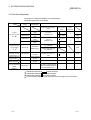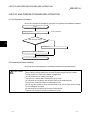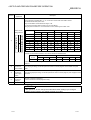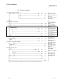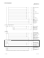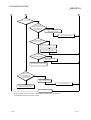
1
U Digital-Analog Converter Module type AJ65VBTCU-68DAV , User s Manual Digital-Analog Converter Module type AJ65VBTCU-68DAV , User s Manual , Digital-Analog Converter Module type A64DAVC/A64DAIC User s Manual MODEL AJ65V-68DA-U-SY-E MODEL CODE 13JR42 SH(NA)-080182-A(0107)MEE HEAD OFFICE : 1-8-12, OFFICE TOWER Z 14F HARUMI CHUO-KU 104-6212,JAPAN NAGOYA WORKS : 1-14 , YADA-MINAMI 5 , HIGASHI-KU, NAGOYA , JAPAN When exported from Japan, this manual does not require application to the Ministry of Economy, Trade and Industry for service transaction permission. Specifications subject to change without notice. Mitsubishi Programmable Controller SAFETY PRECAUTIONS (Always read these precautions before using this equipment.) Before using this product, please read this manual and the relevant manuals introduced in this manual carefully and pay full attention to safety to handle the product correctly. The precautions given in this manual are concerned with this product. Refer to the user's manual of the CPU module to use for a description of the PLC system safety precautions. In this manual, the safety instructions are ranked as "DANGER" and "CAUTION". DANGER Indicates that incorrect handling may cause hazardous conditions, resulting in death or severe injury. ! CAUTION Indicates that incorrect handling may cause hazardous conditions, resulting in medium or slight personal injury or physical damage. ! Note that the ! CAUTION level may lead to a serious consequence according to the circumstances. Always follow the precautions of both levels because they are important to personal safety. Please save this manual to make it accessible when required and always forward it to the end user. [Design Precautions] ! DANGER Configure a safety circuit so that the safety of the overall system is maintained even when an external power error of PLC error occurs. Accident may occur due to output error or malfunctioning. (1) The status of analog output changes depending on the setting of various functions that control the analog output. Take sufficient caution when setting for those functions. For details of analog output status, refer to Section 3.4.1 "Combinations of functions in each part" (2) Normal output may not be obtained due to malfunctions of output elements or the internal circuits. Configure a circuit to monitor signals which may lead to a serious accident. ! CAUTION Do not bunch the control wires or communication cables with the main circuit or power wires, or install them close to each other. They should be installed 100mm (3.9inch) or more from each other. Not doing so could result in noise that would cause erroneous operation. A-1 A-1 [Installation Precautions] ! CAUTION Use the PLC in the environment that meets the general specifications contained in this Manual. Using the PLC outside the range of the general specifications may result in electric shock, fire or malfunction, or may damage or degrade the module. Securely fix the module to a DIN rail or securely fix it with the CC-Link connector type metal installation fitting. Not doing so can cause a drop or malfunction. Do not touch the conducted area or electric parts of the module. Doing so may cause module malfunction or breakdowns. [Wiring Precautions] ! CAUTION Always switch power off externally in all phases before starting installation, wiring and other works. Not doing so can cause the product to be damaged or malfunction. Always ground the FG pin to the protective ground conductor. Not doing so can cause a malfunction. Wire the module correctly after confirming the rated voltage and pin layout of the product. Not doing so can cause a fire or failure. Ensure that no foreign matter such as chips and wire-offcuts enter the module. Foreign matter can cause a fire, failure or malfunction. Do not insert the one-touch connector plug for I/O of the one-touch connector type/connector type compact remote I/O unit into the one-touch connector for analog I/O accidentally. Doing so can cause the module to be damaged. Always fit a non-wired, one-touch connector plug to the open one-touch connector for power supply/FG. Not doing so can cause a failure or malfunction. When connecting the communication and power supply cables to the module, always run them in conduits or clamp them. Not doing so can damage the module and cables due to loose, moved or accidentally pulled cables or can cause a malfunction due to a cable connection fault. When disconnecting the communication and power supply cables from the module, do not hold and pull the cable part. Disconnect the cables after loosening the screws in the portions connected to the module. Pulling the cables connected to the module can damage the module and cables or can cause a malfunction due to a cable connection fault. A-2 A-2 [Starting and Maintenance Precautions] ! CAUTION Do not touch the pin while the power is on. Doing so may cause malfunction. Always start cleaning after switching power off externally in all phases. Not doing so can cause the module to fail or malfunction. Never disassemble or modify the module. This may cause breakdowns, malfunctioning, injury and/or fire. Do not drop the module or give it hard impact since its case is made of resin. Doing so can damage the module. Mount or dismount the module to or from an enclosure after switching power off externally in all phases. Not doing so can cause the module to fail or malfunction. [Disposal Precautions] ! CAUTION When disposing of this product, treat it as industrial waste. A-3 A-3 REVISIONS * The manual number is given on the bottom left of the back cover. Print Date Jul., 2001 Oct., 2001 * Manual Number Revision SH (NA)-080182-A First Printing SH (NA)-080182-B Correction Section 2.3, Section 3.2, Appendix 2 Japanese Manual Version SH-080184-A This manual confers no industrial property rights or any rights of any other kind, nor does it confer any patent licenses. Mitsubishi Electric Corporation cannot be held responsible for any problems involving industrial property rights which may occur as a result of using the contents noted in this manual. 2001 MITSUBISHI ELECTRIC CORPORATION A-4 A-4 INTRODUCTION Thank you for choosing a Mitsubishi MELSEC-A Series General Purpose Programmable Controller. Before using your new PLC, please read this manual thoroughly to gain an understanding of its functions so you can use it properly. CONTENTS SAFETY PRECAUTIONS..............................................................................................................................AREVISIONS ....................................................................................................................................................AAbout Manuals ...............................................................................................................................................AConformation to the EMC Directive and Low Voltage Instruction ................................................................AAbout the Generic Terms and Abbreviations ................................................................................................AProduct Components .....................................................................................................................................A1. OVERVIEW 1 4 7 7 8 9 1- 1 to 1- 3 1.1 Features ................................................................................................................................................... 1- 1 2. SYSTEM CONFIGURATION 2- 1 to 2- 4 2.1 Overall Configuration ............................................................................................................................... 22.2 Applicable System.................................................................................................................................... 22.3 Precautions for System Configuration..................................................................................................... 22.4 Parts Sold Separately .............................................................................................................................. 23. SPECIFICATION 1 2 2 3 3- 1 to 3- 15 3.1 General Specification............................................................................................................................... 3- 1 3.2 Performance Specification....................................................................................................................... 3- 2 3.3 I/O Conversion Characteristics................................................................................................................ 3- 3 3.3.1 Voltage output characteristics........................................................................................................... 3- 4 3.3.2 Relationship between offset/gain setting and analog output value ................................................. 3- 5 3.3.3 Accuracy............................................................................................................................................ 3- 5 3.3.4 Conversion speed ............................................................................................................................. 3- 6 3.4 Function.................................................................................................................................................... 3- 7 3.4.1 Combinations of various functions.................................................................................................... 3- 8 3.5 Remote I/O Signals .................................................................................................................................. 3- 9 3.5.1 Remote I/O signal list ........................................................................................................................ 3- 9 3.5.2 Functions of the remote I/O signals.................................................................................................. 3-10 3.6 Remote Register ...................................................................................................................................... 3-12 3.6.1 Allocation of the remote register ....................................................................................................... 3-12 3.6.2 CH. digital value setting (Addresses RWwm to RWwm+7) ........................................................ 3-13 3.6.3 Analog output enable/disable setting (Address RWwm+8) ............................................................. 3-13 3.6.4 CH. output range setting (Address RWwm+9, RWwm+A) ......................................................... 3-14 3.6.5 HOLD/CLEAR setting (Address RWwm+9, RWwm+B) .................................................................. 3-14 3.6.6 CH. check code (Addresses RWrn to RWrn+7).......................................................................... 3-15 3.6.7 Error code (Address RWrn+8) .......................................................................................................... 3-15 A-5 A-5 4. SETUP AND PREPARATION BEFORE OPERATION 4- 1 to 4- 15 4.1 Pre-Operation Procedure......................................................................................................................... 4- 1 4.2 Precautions When Handling .................................................................................................................... 4- 1 4.3 Name of Each Part................................................................................................................................... 4- 3 4.4 Offset/Gain Setting................................................................................................................................... 4- 6 4.5 Section Number Setting........................................................................................................................... 4- 8 4.6 Facing Direction of the Module Installation ............................................................................................. 4- 8 4.7 Data Link Cable Wiring ............................................................................................................................ 4- 9 4.7.1 Instructions for handling the CC-Link dedicated cables................................................................... 4- 9 4.7.2 Connection of the CC-Link dedicated cables ................................................................................... 4-10 4.8 Wiring........................................................................................................................................................ 4-11 4.8.1 Wiring precautions............................................................................................................................. 4-11 4.8.2 Wiring of module with external equipment ....................................................................................... 4-12 4.9 How to Wire the One-Touch Connector Plug.......................................................................................... 4-13 4.10 Maintenance and Inspection.................................................................................................................. 4-15 5. PROGRAMMING 5- 1 to 5- 13 5.1 Programming Procedure.......................................................................................................................... 5- 1 5.2 Conditions of Program Example.............................................................................................................. 5- 2 5.3 Program Example for Use of the QCPU (Q mode)................................................................................. 5- 4 5.4 Program Example for Use of the QnACPU............................................................................................. 5- 7 5.5 Program Example for Use of the ACPU/QCPU (A mode) (dedicated instructions) .............................. 5- 9 5.6 Program Example for Use of the ACPU/QCPU (A mode) (FROM/TO instructions) ............................. 5-12 6. TROUBLESHOOTING 6- 1 to 6- 5 6.1 Error Code List ......................................................................................................................................... 6- 1 6.2 Using the LED Indications to Check Errors............................................................................................. 6- 2 6.3 Troubleshooting for the Case where the "ERR." LED of the Master Station Flickers ........................... 6- 4 APPENDIX Appendix- 1 to Appendix- 3 Appendix1 Comparison between This Product and AJ65SBT-62DA .............................................Appendix- 1 Appendix2 External dimension diagram...........................................................................................Appendix- 3 INDEX A-6 Index- 1 to Index- 2 A-6 About Manuals The following manuals are also related to this product. In necessary, order them by quoting the details in the tables below. Related Manuals Manual Number (Model Code) Manual Name Control & Communication System Master/Local Module User's Manual type AJ61BT11/A1SJ61BT11 Describes the system configuration, performance specifications, functions, handling, wiring and troubleshooting of the AJ61BT11 and A1SJ61BT11. (Optionally available) Control & Communication System Master/Local Module User's Manual type AJ61QBT11/A1SJ61QBT11 Describes the system configuration, performance specifications, functions, handling, wiring and troubleshooting of the AJ61QBT11 and A1SJ61QBT11. IB-66721 (13J872) IB-66722 (13J873) (Optionally available) Control & Communication System Master/Local Module User's Manual type QJ61BT11 Describes the system configuration, performance specifications, functions, handling, wiring and troubleshooting of the QJ61BT11. SH-080016 (13JL91) (Optionally available) Programming Manual type AnSHCPU/AnACPU/AnUCPU/QCPU-A (A Mode) (Dedicated Instructions) Explains the instructions extended for the AnSHCPU/AnACPU/AnUCPU/QCPU-A (A Mode). IB-66251 (13J742) (Optionally available) Conformation to the EMC Directive and Low Voltage Instruction When complying with EMC Directives and Low-Voltage Directives by assembling a Mitsubishi PLC compatible with EMC Directive and Low-Voltage Directives into the user product, refer to Chapter 3 "EMC Directives and Low-Voltage Directives" in the User’s Manual (Hardware) for the CPU module being used. The CE logo is printed on the rating plate on the main body of the PLC that conforms to the EMC directive and low voltage instruction. To conform this product to the EMC Directive and Low Voltage Directive, refer to the Section of "CC-Link Modules" in Chapter 3 "EMC Directive and Low Voltage Directive" of the User's Manual (Hardware) of the CPU module used. A-7 A-7 About the Generic Terms and Abbreviations Unless otherwise specified, the following generic terms and abbreviations are used in this manual to describe Type AJ65VBTCU-68DAV analog-digital converter module. Generic Term/Abbreviation GX Developer ACPU QnACPU QCPU (A mode) QCPU (Q mode) Master station Local station Remote I/O station Remote device station Remote station Intelligent device station Master module SB SW RX RY RWw RWr A-8 Description Generic product name of the product types SWnD5C-GPPW-E, SWnD5C-GPPW-EA ,SWnD5C-GPPW-EV and SWnD5C-GPPW-EVA (n in the type indicates 4 or more.) Generic term for A0J2CPU, A0J2HCPU, A2CPU, A2CPU-S1, A3CPU, A1SCPU, A1SCPU-S1, A1SCPUC-24-R2, A1SHCPU, A1SJCPU, A1SJCPU-S3, A1SJHCPU, A1NCPU, A2NCPU, A2NCPU-S1, A3NCPU, A3MCPU, A3HCPU, A2SCPU, A2SCPU-S1, A2SHCPU, A2SHCPU-S1, A2ACPU, A2ACPU-S1, A3ACPU, A2UCPU, A2UCPU-S1, A2ASCPU, A2ASCPU-S1, A2ASCPU-S30, A2USHCPU-S1, A3UCPU, A4UCPU Generic term for Q2ACPU, Q2ACPU-S1, Q2ASCPU, Q2ASCPU-S1, Q2ASHCPU, Q2ASHCPU-S1, Q3ACPU, Q4ACPU, Q4ARCPU Generic term for Q02CPU-A, Q02HCPU-A, Q06HCPU-A Generic term for Q00JCPU, Q00CPU, Q01CPU, Q02CPU, Q02HCPU, Q06HCPU, Q12HCPU, Q25HCPU Station that controls the data link system. One master station is required for each system. Station having a PLC CPU and the ability to communicate with the master and other local stations. Remote station that handles bit unit data only. (Performs input and output with external devices.) (AJ65BTB1-16D, AJ65SBTB1-16D) Remote station that handles bit unit and word unit data only. (Performs input and output with external devices, and analog data exchange.) Generic term for remote I/O station and remote device station. (Controlled by the master station) Station that can perform transient transmission, such as the AJ65BT-R2 (including local stations). Generic term for QJ61BT11, AJ61BT11, A1SJ61BT11, AJ61QBT11, and A1SJ61QBT11 when they are used as master stations. Link special relay (for CC-Link) Bit unit information that indicates the module operating status and data link status of the master station/local station. (Expressed as SB for convenience) Link special register (for CC-Link) 16 bit unit information that indicates the module operating status and data link status of the master station/local station. (Expressed as SW for convenience) Remote input (for CC-Link) Information entered in bit units from the remote station to the master station. (Expressed as RX for convenience) Remote output (for CC-Link) Information output in bit units from the master station to the remote station. (Expressed as RY for convenience) Remote register (Write area for CC-Link) Information output in 16-bit units from the master station to the remote device station. (Expressed as RWw for convenience) Remote register (Read area for CC-Link) Information entered in 16-bit units from the remote device station to the master station. (Expressed as RWr for convenience) A-8 Product components This product consists of the following. Product Name Type AJ65VBTCU-68DAV digital-analog converter module Type AJ65VBTCU-68DAV digital-analog converter module user's manual (hardware) A-9 Quantity 1 1 A-9 1 OVERVIEW MELSEC-A 1 OVERVIEW 1 This user's manual explains the specifications, handling, programming methods and others of Type AJ65VBTCU-68DAV digital-analog converter module (hereafter abbreviated to the " AJ65VBTCU-68DAV ") which is used as a remote device station of a Control & Communication Link (hereafter abbreviated to "CC-Link") system. The AJ65VBTCU-68DAV is a module designed to convert digital values (16-bit signed BIN data) from outside the PLC into analog values (voltages or currents). This module is a voltage output-dedicated model. 1.1 Features This section gives the features of the AJ65VBTCU-68DAV. (1) High accuracy This module performs D/A conversion at the accuracy of ±0.3% relative to the maximum value of the analog output value at the operating ambient temperature of 0 to 55°C, or at ±0.2% relative to the maximum value of the analog output value at the operating ambient temperature of 25±5°C. (2) Output range selectable per channel You can choose the analog output range per channel to change the I/O conversion characteristics. (3) High resolution of 1/±4000 By changing the output range, you can choose and set the resolution to either 1/4000 or 1/±4000 (when the -10 to +10V range or user range setting 1 is selected) to provide high-resolution analog values. (4) Setting of analog output hold or clear at STOP of PLC CPU You can specify whether to hold or clear the analog value which is being output from each channel of the unit when the PLC CPU has entered the STOP mode or the AJ65VBTCU-68DAV has stopped D/A conversion due to error occurrence. (5) More channels than those of the conventional D/A converter modules The number of channels is four times greater than that of the conventional CCLink A/D converter module (AJ65SBT-62DA). 1-1 1-1 1 OVERVIEW MELSEC-A (6) Sharply reducible wiring man-hours Wiring man-hours can be reduced sharply by adopting individual wire insulation displacement termination type one-touch connectors (no need for soldering, shield peeling and screwing) to connect the communication and power supply cables. Connector Soldering, peeling of the shield and screwing are unnecessary. Push in Each of the individual wires can be securely connected simply by pressing the side surface of the connector plug after the wires are inserted into the connector. (7) Significant improvement of wiring performance The above one-touch connectors for IN and OUT sides are plugged individually, greatly improving the performance of jumper wiring especially in an enclosure. (Mixed jumper wiring of the power supply cables with the I/O modules is not allowed.) 1-2 1-2 1 1 OVERVIEW MELSEC-A (8) Replacement of module without stopping CC-Link system The use of the online connectors (for communication, for power supply) allows the module to be changed without the CC-Link system being stopped. Online connector for communication (A6CON-LJ5P) One-touch connector plug for communication (A6CON-L5P) Online connector for power supply/FG (A6CON-PWJ5P) One-touch connector plug for power supply/FG (A6CON-PW5P) (9) Improved wiring workability The connectors and setting switches are all front-mounted. This enables connections to be made only by front wiring, improving wiring workability. It also allows setting to be made after installation to an enclosure. 1-3 1-3 2 SYSTEM CONFIGURATION MELSEC-A 2 SYSTEM CONFIGURATION This chapter describes the system configuration for use of the AJ65VBTCU-68DAV. 2.1 Overall Configuration 2 The overall configuration for use of the AJ65VBTCU-68DAV is shown below. CC-Link master/local module (master station) (AJ61BT11, A1SJ61BT11, AJ61QBT11, A1SJ61QBT11, QJ61BT11) CC-Link master/local module (local station) (AJ61BT11, A1SJ61BT11, AJ61QBT11, A1SJ61QBT11, QJ61BT11) Ver.1.10 compatible CC-Link dedicated cable (Intelligent device station) AJ65VBTCU-68DAV (Remote device station) (Remote I/O station) (Remote device station) 3 station occupied RX/RY: 32 points each RWr/RWw: 12 points each Object whose voltage will be detected 2-1 2-1 2 SYSTEM CONFIGURATION MELSEC-A 2.2 Applicable System This section explains the applicable system. (1) Applicable master modules The following master modules can be used with the AJ65VBTCU-68DAV. AJ61BT11 A1SJ61BT11 AJ61QBT11 A1SJ61QBT11 QJ61BT11 2 (2) Restrictions on use of CC-Link dedicated instructions (RLPA, RRPA) The CC-Link dedicated instructions may not be used depending on the PLC CPU and master module used. For details of the restrictions, refer to the A series master module user's manual, and the Programing Manual type AnSHCPU/AnACPU/AnUCPU/QCPU (A mode) (Dedicated Instructions). This module does not allow the use of the dedicated instructions other than RLPA and RRPA. Refer to Section 5.5 for a program example using the dedicated instructions (RLPA, RRPA). 2.3 Precautions for System Configuration Before powering off or changing this module, stop the control of the mating equipment. 2-2 2-2 2 SYSTEM CONFIGURATION MELSEC-A 2.4 Parts Sold Separately The plugs for AJ65VBTCU-68DAV are sold separately. Please purchase them as necessary. Mitsubishi model name Part model name (manufacturer) Applicable cable core size (mm2) Plug for one-touch connector 1, 4 A6CON-P214 A6CON-P220 A6CON-P514 A6CON-P520 One-touch connector plug for communication 2, 4 A6CON-L5P 33104-6000FL (3M) 33104-6100FL (3M) 33104-6200FL (3M) 33104-6300FL (3M) 35505-6000BOM GF (3M) 0.14 to 0.2 (AWG#26 to 24) 0.3 to 0.5 (AWG#22 to 20) communication line 0.5 (AWG#20) 2-3 Applicable cable outer diameter (mm) Maximum rated current (A) 1.0 to 1.4 Transparent 2 1.4 to 2.0 Yellow 1.0 to 1.4 Red 3 1.4 to 2.0 Blue 2.2 to 3.0 Red shielded cable (drain wire) 0.5 (AWG#20) 0.75 (0.66 to 0.98) (AWG#18) One-touch 35505-6080-A00 wire diameter 0.16 mm or connector for power A6CON-PW5P GF (3M) more supply/FG 2, 4 Online connector for 35720-L200-B00 A6CON-LJ5P communication 3 AK (3M) 35720-L200-A00 Online connector for A6CON-PWJ5P AK (3M) power supply/FG 3 One-touch connector One-touch connector plug with plug with terminating A6CON-TR11 terminating resister attached resistor for communication (110Ω) (including 1) 1 2 3 4 Color of the cover Specifications 2.2 to 3.0 7 Gray Mitsubishi's A6CON-P includes 20 plugs. Mitsubishi's A6CON- 5P includes 10 plugs. Mitsubishi's A6CON- J5P includes 5 plugs. Once insulation-displaced, the one-touch connector plugs cannot be reused. 2-3 2 SYSTEM CONFIGURATION MELSEC-A REMARK The following table indicates the connectors of this module with which the above plugs/connectors are compatible. Connector of This Module One-touch connector for communication One-touch connector for power 2-4 Compatible Optional Parts • One-touch connector plug for communication • Online connector for communication • One-touch connector plug with terminating resistor • One-touch connector plug for power supply/FG supply/FG • Online connector for power supply/FG One-touch connector for analog I/O • Plug for one-touch connector 2-4 3 SPECIFICATION MELSEC-A 3 SPECIFICATION This chapter provides the specifications of the AJ65VBTCU-68DAV. 3.1 General Specification Table 3.1 indicates the general specifications of the AJ65VBTCU-68DAV. Table 3.1 General specification Item Specification Usage ambient temperature 3 0 to 55°C Storage ambient temperature -20 to 75°C Usage ambient humidity 10 to 90%RH, no condensation Storage ambient humidity 10 to 90%RH, no condensation When there is intermittent vibration Conforming to JIS B 3501, IEC 61131-2 Vibration durability Shock durability Frequency Acceleration Amplitude 10 to 57Hz — 0.075mm (0.0030inch) 57 to 150Hz 9.8m/s2 — When there is continuous vibration Frequency Acceleration Amplitude 10 to 57Hz — 0.035mm (0.0013inch) 57 to 150Hz 4.9m/s2 — Sweep count 10 times in each direction X, Y, Z (80 minutes) Conforming to JIS B 3501, IEC61131-2 (147m/s2, 3 times each in 3 directions) Usage environment Usage height No corrosive gas Less than 2000 m (less than 6562 ft.) Installation area Within the control board Over-voltage category *1 2 Pollution level * Less than II Less than 2 *1 Indicates the location where the device is connected from the public cable network to the device structure wiring area. Category II applies to the devices to which the power is supplied from a fixed equipment. Surge withstand voltage for devices with up to 300V of rated voltage is 2500V. *2 This is an index which indicates the degree of conductive object generation in the environment Pollution level 2 is when only non-conductive pollution occurs. A temporary conductivity caused by condensation must be expected occasionally. 3-1 3-1 3 SPECIFICATION MELSEC-A 3.2 Performance Specification Table 3.2 indicates the performance specifications of the AJ65VBTCU-68DAV. Table 3.2 Performance Specifications Item AJ65VBTCU-68DAV IP1XB Protection class 16-bit signed binary (-4096 to +4095) Digital input Analog output 3 I/O characteristics, maximum resolution, accuracy (accuracy relative to maximum value of analog output value) Maximum conversion speed Output short-circuit protection Absolute maximum output Number of analog output points CC-Link station type Number of occupied stations Communication cable Dielectric withstand voltage Insulation method Noise durability External wiring system One-touch connector for communication One-touch Applicable connector for power supply/FG wire size One-touch connector for analog I/O Applicable DIN rail External supply power Weight 3-2 -10 to +10VDC (external load resistance: 2k to 1M ) Voltage Accuracy Digital Input Max. Analog Output Range Ambient temperature Ambient temperature Value Resolution 0 to 55°C 25±5°C -10 to +10V -4000 to ±0.3% ±0.2% 2.5mV User range setting 1 +4000 (±30mV) (±20mV) (-10 to +10V) 0 to 5V 1.25mV ±0.3% ±0.2% 1 to 5V 0 to 4000 (±15mV) (±10mV) 1.0mV User range setting 2 (0 to 5V) 1ms/1 channel Provided ±12V 8 channels/1 module Remote device station 3 station (RX/RY: 32 points each, RWr/RWw: 12 points each) Ver. 1.10 compatible CC-Link dedicated cable FANC-110SBH, FA-CBL200PSBH, CS-110 500VAC for 1 minute across all power supply and communication system terminals and all analog output terminals Across communication system terminals and all analog output terminals: Photocoupler isolated Across power supply system terminals and all analog output terminals: Photocoupler isolated Across channels: Non-isolated By noise simulator of 500Vp-p noise voltage, 1µs noise width and 25 to 60Hz noise frequency One-touch connector for communication [Transmission circuit] (5 pins pressure welding type, the plug for the connector is sold separately) One-touch connector for power supply and FG [Unit power supply and FG] (5 pins pressure welding type, the plug for the connector is sold separately) One-touch connector for analog I/O (4 pins pressure welding type, the plug for the connector is sold separately) <Sold separately> Online connector for communication : A6CON-LJ5P Online connector for power supply : A6CON-PWJ5P Communication line : Ver. 1.10 compatible CC-Link dedicated cable 0.5mm2 (AWG#20) [ 2.2 to 3.0], shielded wire 0.5mm2 (AWG#20) 0.66 to 0.98 mm2 (AWG#18) [ 2.2 to 3.0] Wire diameter 0.08 mm2 or more 1.0 to 1.4 (A6CON-P214), 1.4 to 2.0 (A6CON-P220) [Applicable cable : 0.14 to 0.2 mm2] 1.0 to 1.4 (A6CON-P514), 1.4 to 2.0 (A6CON-P520) [Applicable cable : 0.3 to 0.5 mm2] TH35-7.5Fe, TH35-7.5Al (conforming to JIS C 2812) CC-Link connector type metal installation fitting : A6PLT-J65V1 DC24V (DC20.4V to DC26.4V, ripple factor within 5%) Inrush current : 4.3A, within 1.2ms Current consumption 0.15A 0.16kg 3-2 3 SPECIFICATION MELSEC-A 3.3 I/O Conversion Characteristics An I/O conversion characteristic indicates an inclination of a straight line which connects an offset value and a gain value at the time when a digital value set from the PLC CPU is converted into an analog value (voltage or current output). The offset value is an analog value (voltage) output when the digital value set from the PLC CPU is 0. The gain value is an analog value (voltage) output when the digital value set from the PLC CPU is 4000. 3-3 3-3 3 SPECIFICATION MELSEC-A 3.3.1 Voltage output characteristics The voltage output characteristic graph is shown below. 1 5 Practical analog output scope Analog output voltage (V) 10 3 1 2 0 -5 -10 -4096 -4000 -2000 0 2000 4000 4095 Digital input value Number Analog Output Range Setting Offset Value Gain Value Digital Input Value Maximum Resolution 1) -10 to +10v 0V 10V -4000 to +4000 2.5mV 2) 0 to 5V 0V 5V 3) 1 to 5V 1V 5V — User range setting 1 (-10 to +10v) 0V 10V -4000 to +4000 2.5mV — User range setting 2 (0 to 5v) 0V 5V 0 to 4000 1.0mV 0 to 4000 1.25mV 1.0mV Fig. 3.1 Voltage Output Characteristic POINT (1) Within the digital input and analog output scopes of each output range, the maximum resolution and accuracy are within the performance specification range. Outside those scopes, however, they may not fall within the performance specification range. (Avoid using the dotted line part in Fig. 3.1.) (2) Set the offset and gain values of the user range setting within the range satisfying the following conditions. (a) Setting range when user range setting 1 is selected: -10 to +10V (b) Setting range when user range setting 2 is selected: 0 to 5V (c) (Gain value) > (Offset value) If you attempt to make setting outside the setting range of (a) or (b), the "RUN" LED flickers at 0.5s intervals. Set the values within the setting range. If you attempt to make setting outside the setting range of (c), the "RUN" LED flickers at 0.5s intervals. Make setting again. 3-4 3-4 3 SPECIFICATION MELSEC-A 3.3.2 Relationship between offset/gain setting and analog output value How to calculate the analog output value: The resolution of AJ65VBTCU-68DAV can be set arbitrarily by modifying the setting of the offset value and gain value. How to calculate the analog value resolution and the analog output value for a given digital input value when the settings of the offset value and gain value are changed is shown next. (1) Resolution Find the resolution with the following expression. (Analog resolution) = (Gain value) - (Offset value) 4000 (2) Analog output value Find the analog output value with the following expression. (Analog output) = (Analog resolution) × (Digital input value) + (Offset value) 3.3.3 Accuracy Accuracy is relative to the maximum value of the analog output value. If you change the offset/gain setting or output range to change the output characteristic, accuracy does not change and is held within the range indicated in the performance specifications. (1) Accuracy of voltage output For voltage output, the maximum value of the analog output value changes with the range. For example, accuracy is relative to 5V when the 0 to 5V range is selected. Analog output is provided at the accuracy of within ±0.2% (±10mV) when the operating ambient temperature is 25±5°C, or within ±0.3% (±15mA) when the operating ambient temperature is 0 to 55°C. 5V Analog output voltage Varies within the range of 0.2% ( 10mV) at operating ambient temperature of 25 5 . Varies within the range of 0.3% ( 15mV) at operating ambient temperature of 0 to 55 . 0V 0 4000 Digital input value Fig. 3.2 Voltage Output Accuracy (When 0 to 5V Range Is Selected) 3-5 3-5 3 SPECIFICATION MELSEC-A 3.3.4 Conversion speed Conversion speed indicates time required to read the digital output value written to the buffer memory, perform D/A conversion, and then output the specified analog value. Conversion speed per channel of the AJ65VBTCU-68DAV is 1ms. Due to the data link processing time of the CC-Link system, there is a transmission delay until the D/A conversion value is read actually. For the data link processing time, refer to the user's manual of the master module used. Example) Data link processing time taken in the asynchronous mode when the master module is the QJ61BT11 (normal value) [Calculation expression] SM+LS×1+remote device station processing time SM: Scan time of master station sequence program LS : Link scan time Remote device station processing time: (Number of channels used+1 ) × 1ms : Internal processing time of AJ65VBTCU-68DAV 3-6 3-6 3 SPECIFICATION MELSEC-A 3.4 Function Table 3.3 lists the functions of the AJ65VBTCU-68DAV. Table 3.3 AJ65VBTCU-68DAV Function List Item Description Refer to D/A output enable/disable function Specify whether the D/A conversion value is output or the offset value is output per channel. Note that the conversion speed is constant independently of the output enable/disable setting. Section 3.5.2 D/A conversion enable/disable function Specify whether D/A conversion is enabled or disabled per channel. The sampling cycle can be shortened by setting the unused channel to D/A conversion disable. Section 3.6.3 You can set the analog output range per channel to change the I/O conversion characteristics. Select the output range setting from among the following 8 types. Output range changing function Output Range Set Value -10 to +10V 0H 0 to 5V 1H 1 to 5V 2H User range setting 1 (-10 to +10V) 3H User range setting 2 (0 to 5V) 4H Section 3.6.4 Function to specify hold or clear of the analog output when the PLC CPU is in the STOP status (HOLD/CLEAR setting) Specify per channel whether to hold or clear (output the offset value) the analog value which is being output from each channel when the PLC CPU has entered the STOP status or the AJ65VBTCU-68DAV has stopped D/A conversion due to error occurrence. Section 3.6.5 Offset/gain setting You can make offset/gain setting per channel without potentiometers to change the I/O conversion characteristics freely. Section 4.4 3-7 3-7 3 SPECIFICATION MELSEC-A 3.4.1 Combinations of various functions You can set the analog output as indicated in Table 3.4 by combining the Analog output enable/disable setting (RWwm+8), CH. analog output enable/disable flag (RYn0 to RYn7) and HOLD/CLEAR setting (RWwm+B). Make setting according to your system application. Table 3.4 Analog output status combination list Setting Analog output enable/disable combisetting (RWwm+8) nation CH. analog output enable/ Exedisable flag (RYn0 to RYn7) cution status HOLD/CLEAR setting (RWwm+B) Analog output status when the PLC CPU is in the RUN status Enable (1) Enable (ON) HOLD CLEAR Output of the analog value after D/A conversion from the digital value specified by the PLC CPU Prohibit (0) Prohibit (OFF) Enable or disable HOLD or CLEAR HOLD or CLEAR Offset value 0V Analog output status when the PLC CPU is in the STOP status Analog value before the PLC CPU stop is retained Offset value Offset value 0V Analog output status at PLC CPU stop error Analog value before the PLC CPU stop is retained Offset value Offset value 0V Offset value 0V Offset value 0V Analog output status at occurrence of AJ65VBTCU- Output of the maximum or minimum analog 68DAV digital value setting error value Analog output status when the "L RUN" LED turns off/"L.ERR" LED turns on The analog value before the "L RUN" LED turns off is retained. Analog output status when the "L ERR." LED flickers Output of the analog value after D/A conversion from the digital value specified by the PLC CPU Offset value 0V Analog output status in initial processing completion status after power-reset Output of the analog value after D/A conversion from the digital value specified by the PLC CPU Offset value 0V Offset value Analog output status at occurrence of AJ65VBTCU68DAV output range setting error 0V 0V 0V 0V Analog output status at occurrence of AJ65VBTCU68DAV watchdog timer error 0V 0V 0V 0V POINT When the QnACPU is used, using "Y" as the remote output (RY) refresh device of the automatic refresh parameter may not hold the analog value even for the HOLD setting. For the HOLD setting, use "M" or "B" as the remote output (RY) refresh device. 3-8 3-8 3 SPECIFICATION MELSEC-A 3.5 Remote I/O Signals This section describes the assignment and functions of the remote I/O signals. 3.5.1 Remote I/O signal list Remote inputs (RX) mean the input signals from the AJ65VBTCU-68DAV to the master module, and remote outputs (RY) mean the output signals from the master module to the AJ65VBTCU-68DAV. In communications with the master station, the AJ65VBTCU-68DAV uses 32 points of the remote inputs (RX) and 32 points of the remote outputs (RY). This module occupies three stations but do not use the latter 64 points. Table 3.5 indicates the assignment and names of the remote I/O signals. Table 3.5 Remote I/O Signals List Signal Direction: AJ65VBTCU-68DAV Remote input (RX) RXn0 to RXnB Master Module Name Reserved E2PROM write error flag Signal Direction: Master Module AJ65VBTCU-68DAV Remote output (RY) Name RYn0 CH.1 analog output enable/disable flag RYn1 CH.2 analog output enable/disable flag RYn2 CH.3 analog output enable/disable flag RYn3 CH.4 analog output enable/disable flag RYn4 CH.5 analog output enable/disable flag RYn5 CH.6 analog output enable/disable flag RYn6 CH.7 analog output enable/disable flag RYn7 CH.8 analog output enable/disable flag Reserved RXnD to RX (n+1) 7 Reserved RYn8 to RY (n+1) 7 RX (n+1) 8 Initial data processing request flag RY (n+1) 8 Initial data processing complete flag RX (n+1) 9 Initial data setting complete flag RY (n+1) 9 Initial data setting request flag RX (n+1) A Error status flag RY (n+1) A Error reset request flag RX (n+1) B Remote READY RX (n+1) C to RX (n+1) F Reserved RY (n+1) B to RY (n+1) F Reserved RXnC POINT The reserved devices given in Table 3.5 are used by the system and cannot be used by the user. If the user has used (turned on/off) any of them, we cannot guarantee the functions of the AJ65VBTCU-68DAV. 3-9 3-9 3 SPECIFICATION MELSEC-A 3.5.2 Functions of the remote I/O signals Table 3.6 explains the functions of the remote I/O signals of the AJ65VBTCU-68DAV. Table 3.6 Remote I/O Signal Details (1/2) Device No. Signal Name Description Turns on the number of E2PROM write times exceeds its limit (1000,000 times per RXnC 2 E PROM write error flag channel). If this flag has turned on, this module itself has failed (hardware fault) and therefore this flag cannot be reset (turned off) by the error reset request flag. At occurrence of this error, power on the AJ65VBTCU-68DAV again. If this flag turns on after the power is switched on again, it is a hardware fault. Contact your nearest Mitsubishi representative. After power-on, the initial data processing request flag is turned on by the AJ65VBTCU68DAV to request the initial data to be set. Also, after the initial data processing is complete (initial data processing complete flag RY (n+1) 8 ON), the flag is turned off. RX(n+1)8 Initial data processing request flag RY(n+1)8 Initial data processing complete flag RX (n+1) 8 Initial data processing request flag RX(n+1)9 Initial data setting complete flag RY(n+1)9 Initial data setting request flag RX(n+1)B Remote ready : Performed by sequence ladder : Performed by AJ65VBTCU-68DAV RX (n+1) 9 Initial data setting complete flag When the initial data setting request (RY (n+1) 9 ON) is made, the flag turns on after the initial data setting completion is done. Also, after the initial data setting is complete, the initial setting complete flag turns off when the initial data setting request flag turns off. Turns on at occurrence of the output range setting error, digital value setting error or E2PROM write error (RXnC). Does not turn on at occurrence of the watchdog timer error. (The "RUN" LED goes off.) RX (n+1) A Error status flag RX(n+1)A Error status flag RY(n+1)A Error reset request flag RWrn+8 Error code 0 Error code 0 RWrn to RWrn+7 CH. check code 0 Check code 0 : Performed by sequence ladder : Performed by AJ65VBTCU-68DAV RX (n+1) B Remote READY Turns on when initial data setting is completed after power-on or at termination of the test mode. (Used for interlocking read/write from/to the master module.) n: Address allocated to the master module by station number setting. 3 - 10 3 - 10 3 SPECIFICATION MELSEC-A Table 3.6 Remote I/O Signal Details (2/2) Device No. Signal Name Description CH. analog output enable/disable flag D/A conversion value output enable flag for channel 1 to 8. Turn on this flag to enable the D/A conversion value of the corresponding channel to be output. Turn off when you want to disable the output of the D/A conversion value. Processed on the leading edge of ON/OFF. RY (n+1) 8 Initial data processing complete flag Turns on after initial data processing completion when initial data processing is requested after power-on or test mode operation. RY (n+1) 9 Initial data setting request flag RYn0 to RYn7 RY (n+1) A Error reset request flag Turns on at the time of initial data setting or changing. Turning on this flag resets (turns off) the error status flag (RX(n+1)A) and also clears (to check code (RWrn to RWrn+7) in the 0000H) the error code (RWrn+8) and CH. remote register. However, since the E2PROM write error flag (RXnC) cannot be reset, the error status flag remains on, too. n: Address allocated to the master module by station number setting. 3 - 11 3 - 11 3 SPECIFICATION MELSEC-A 3.6 Remote Register The AJ65VBTCU-68DAV has a remote resister for data communication with the master module. The remote register allocation and data structures are described below. 3.6.1 Allocation of the remote register The allocation of the remote register is shown in Table 3.7. Table 3.7 Allocation of the remote register Transfer Direction Master Remote Remote Master Address Description Default Value RWwm CH. 1 digital value setting 0 RWwm+1 CH. 2 digital value setting 0 RWwm+2 CH. 3 digital value setting 0 RWwm+3 CH. 4 digital value setting 0 RWwm+4 CH. 5 digital value setting 0 RWwm+5 CH. 6 digital value setting 0 RWwm+6 CH. 7 digital value setting 0 RWwm+7 CH. 8 digital value setting 0 RWwm+8 Analog output enable/disable setting 0 RWwm+9 CH. 1 to 4 output range setting 0 RWwm+A CH. 5 to 8 output range setting 0 RWwm+B HOLD/CLEAR setting 0 RWrn CH. 1 check code 0 RWrn+1 CH. 2 check code 0 RWrn+2 CH. 3 check code 0 RWrn+3 CH. 4 check code 0 RWrn+4 CH. 5 check code 0 RWrn+5 CH. 6 check code 0 RWrn+6 CH. 7 check code 0 RWrn+7 CH. 8 check code 0 RWrn+8 Error code 0 RWrn+9 to RWrn+B Reserved 0 Refer to Section 3.6.2 Section 3.6.3 Section 3.6.4 Section 3.6.5 Section 3.6.5 Section 3.6.7 m, n: The address set for the master station in the station number setting. POINT Do not execute read or write to the remote register that is not allowed to use. When a read or write is executed, the functions of the AJ65VBTCU-68DAV is not guaranteed. 3 - 12 3 - 12 3 SPECIFICATION 3.6.2 CH. MELSEC-A digital value setting (Addresses RWwm to RWwm+7) (1) This area is used to write the digital value for the D/A conversion from the PLC CPU. (2) The digital value at all channels become “0” in the following conditions: (a) After the power is turned on, when the remote READY (RX(n+1)B) is turned on. (3) The digital value that may be set is a 16-bit signed binary within the setting range which matches the output range setting. If a value beyond the range of the digital value resolution is set, the data in Table 3.8 is applied for the D/A conversion. In addition, the checking code is stored in the check code storage area (addresses RWrn to RWrn+7). Table 3.8 Available setting range of the digital value Output Range Available setting range Digital value for the D/A conversion when the value beyond the range is set -10 to +10V User range setting 1 -4096 to +4095 (Practical scope: -4000 to +4000) 4096 or more: 4095 -4097 or less: -4096 0 to 5V 1 to 5V User range setting 2 -96 to 4095 (Practical scope: 0 to 4000) 4096 or more: 4095 -97 or less: -96 3.6.3 Analog output enable/disable setting (Address RWwm+8) (1) Set whether D/A conversion is enabled or disabled per channel. (2) Operation is performed according to the setting made for the leading edges of initial data setting request flag (RY(n+9)). (3) The default setting is conversion enable for all channels. b15 b14 b13 b12 b11 b10 b9 b8 b7 b6 b5 b4 b3 b2 b1 b0 CH.8 CH.7 CH.6 CH.5 CH.4 CH.3 CH.2 CH.1 Ignored 3 - 13 0: Conversion disable 1: Conversion enable 3 - 13 3 SPECIFICATION 3.6.4 CH. MELSEC-A output range setting (Address RWwm+9, RWwm+A) (1) Set the analog output range per channel. (2) Operation is performed according to the setting made for the leading edges of initial data setting request flag (RY(n+9)). (3) The default settings are -10 to +10V for all channels. b15 RWwm+9 to b12 b11 to b15 RWwm+A b12 to b8 b7 to CH.3 CH.4 b11 to CH.8 b4 b3 CH.2 b8 b7 to CH.7 b4 b3 CH.6 Output range Seting value -10 to +10V 0H 0 to 5V 1H 1 to 5V 2H User range setting 1 (-10 to +10V) 3H User range setting 2 (0 to 5V) 4H to b0 CH.1 to b0 CH.5 POINT If the set value is outside the setting range, error "20 " occurs, the "RUN" LED flickers at intervals of 0.1s, and all channels do not make D/A conversion. indicates the channel No. where the error occurred. 3.6.5 HOLD/CLEAR setting (Address RWwm+9, RWwm+B) (1) Set HOLD/CLEAR to each channel. (2) Operation is performed according to the setting made for the leading edges of initial data setting request flag (RY(n+9)). (3) The default settings are CLERA for all channels. b15 b14 b13 b12 b11 b10 b9 b8 b7 b6 b5 b4 b3 b2 b1 b0 CH.8 CH.7 CH.6 CH.5 CH.4 CH.3 CH.2 CH.1 Ignored 3 - 14 0: CLEAR 1: HOLD 3 - 14 3 SPECIFICATION 3.6.6 CH. MELSEC-A check code (Addresses RWrn to RWrn+7) (1) This area is used to check if the digital value is within or out of the setting range. One of the following checking codes is stored when the digital value lower or higher than the setting range is set. Check code Description 000FH A digital value which exceeds the setting range was set. 00F0H A digital value which is below the setting range was set. 00FFH The digital value less than the setting range and the digital value more than the setting range were set before the error reset request. (2) The check code once stored is not reset even if the set value is set to within the valid setting allowed range. (3) The storage area or the check code is reset by turning on the error reset request flag (RY (n+1)A). 3.6.7 Error code (Address RWrn+8) If an error occurs (the RUN LED flickers) when data is written to the AJ65VBTCU68DAV, the corresponding error code is stored into the remote register (address RWrn+8) of the AJ65VBTCU-68DAV. Refer to Section 6.1 for details of the error codes. 3 - 15 3 - 15 4 SETUP AND PREPARATION BEFORE OPERATION MELSEC-A 4 SETUP AND PREPARATION BEFORE OPERATION 4.1 Pre-Operation Procedure This section explains the preparatory procedure for operating the AJ65VBTCU-68DAV. START Create Create a a program. program. .......Refer to Chapter 5. Make offset/gain setting? 4 No Yes Start data link. Offset/gain setting (Refer to Section 4.4.) END 4.2 Precautions When Handling The precautions when handling the AJ65VBTCU-68DAV are described below: CAUTION 4-1 Do not touch the pins while power is on. Doing so can cause a malfunction. Ensure that no foreign matter such as chips and wire-offcuts enter the module. Foreign matter can cause a fire, failure or malfunction. Do not disassemble or modify the module. Doing so can cause a failure, malfunction, injury or fire. Do not touch the conductive and electronic parts of the module directly. Doing so can cause the module to malfunction or fail. Do not drop the module or give it hard impact since its case is made of resin. Doing so can damage the module. Do not touch the conductive parts of the module directly. Doing so can cause the module to malfunction or fail. 4-1 4 SETUP AND PREPARATION BEFORE OPERATION CAUTION MELSEC-A Dispose of the product as industrial waste. Use the module in the environment indicated in the general specifications given in this manual. Not doing so can cause an electric shock, fire, malfunction, product damage or deterioration. Securely fix the module to a DIN rail or securely fix it with the CC-Link connector type fitting. Not doing so can cause a drop or malfunction. Mount or dismount the module to or from an enclosure after switching power off externally in all phases. Not doing so can cause the module to fail or malfunction. (1) When using the DIN rail adapter, install the DIN rail by making sure of the following: (a) Applicable DIN rail models (conforming to the JIS C 2812) TH35-7.5Fe TH35-7.5Al 4 (b) DIN rail installation screw interval When installing the DIN rail, tighten the screws with less than 200mm (7.87 inch) pitches. (2) As the CC-Link connector type metal installation fitting, use the narrow-width type (width 41)-dedicated fitting. (a) CC-Link connector type metal installation fitting model A6PLT-J65V1 (3) Refer to the Master Module user's manual for the name, specification, and manufacturers of supported cables for the use with AJ65VBTCU-68DAV. 4-2 4-2 4 SETUP AND PREPARATION BEFORE OPERATION MELSEC-A 4.3 Name of Each Part The name of each part in the AJ65VBTCU-68DAV is shown. [Pin layout and signals name] Pin arrangement Pin No. 1 AJ65VBTCU-68DAV CON A L I N CON K B 8) C H 1 2 CONA, B 3) SEL CON1 2 NC 3 CH1 COM NC 3 CH2 COM 5 4 3 2 1 CON2 CONA CONB 4) 4321 CON1 CON3 CON2 2) CON3 CON4 CON4 CON5 7 6), 7) 8 CON6 CON5 CON7 MODE 5) CON P C O W E CON R D CON8 5 4 3 21 CON6 CONC COND A module view from the top CON7 11) CON8 CONC, D 4-3 CH1 V+ 2 1) GAIN 9) 1 RUN OFFSET 6 NC SLD NC 1 2 4 8 5 4 5 CH2 V+ TEST 10) DG 4 DOWN L ERR SW1 4 DB 3 1 L RUN 3 DA 2 POWER SET UP Signal name 4 NC 1 CH3 V+ 2 NC 3 CH3 COM 4 NC 1 CH4 V+ 2 NC 3 CH4 COM 4 NC 1 CH5 V+ 2 NC 3 CH5 COM 4 NC 1 CH6 V+ 2 NC 3 CH6 COM 4 NC 1 CH7 V+ 2 NC 3 CH7 COM 4 NC 1 CH8 V+ 2 NC 3 CH8 COM 4 NC 1 FG 2 +24V(UNIT) 3 24G(UNIT) 4 NC 5 NC 4-3 4 SETUP AND PREPARATION BEFORE OPERATION Name and appearance Number Description POWER LED ON : Power supply on OFF : Power supply off Normal mode On : Normal operation Flashing : 0.1s intervals indicate an output range setting error, mode select switch setting error. 0.5s intervals indicate a digital value setting error. Off :24VDC power supply shutoff or watchdog timer error occurred. Test mode On : Indicate that the SELECT/SET switch is in the SET position. Flashing : 0.5s intervals: An attempt was made to make setting outside the setting range at the time of offset/gain setting. Off : Indicates that the SELECT/SET switch is in the SELECT or center position. RUN LED 1) 2) Operation status display LED Offset/gain adjusting LEDs MELSEC-A L RUN LED On : Normal communication Off : Communication cutoff (time expiration error) L ERR. LED On : Indicates that transmission speed setting or station number setting is outside the range. Flicker at fixed intervals : Indicates that transmission speed setting or station number setting was changed from that at power-on. Flicker at unfixed intervals : Indicates that you forgot fitting the terminating resistor or the module or CC-Link dedicated cable is affected by noise. Off : Indicates normal communications. TEST CH Normal mode Normally OFF. OFFSET GAIN Test mode TEST : ON The OFFSET/GAIN/ CH LEDs lit change every time the SELECT/SET switch is moved to SELECT. (Refer to section 4.4) 3) SELECT/SET switch Used to make offset/gain setting in the test mode. 4) UP/DOWN switch Used to adjust the offset value and gain value of the channel specified by the SELECT/SET switch. 5) Mode select switch 0: Normal mode 1: Test mode (user range setting 1) 2: Test mode (user range setting 2) 3 to 7: Must not be used Setting Switches Set Value 6) 4-4 B RATE 1 2 4 Transmission speed setting switches Transmission Speed 4 2 1 0 OFF OFF OFF 156kbps 1 OFF OFF ON 625kbps 2 OFF ON OFF 2.5Mbps 3 OFF ON ON 5.0Mbps 4 ON OFF OFF 10Mbps Always set the transmission speed within the above range. The switches are all factory-set to OFF. Making any other setting than the above will result in an error flickering the "L ERR." LED. Confirm the transmission speed setting switch numbers on the seal located on the side face of the connector for analog I/O. 4-4 4 SETUP AND PREPARATION BEFORE OPERATION Name and appearance Number MELSEC-A Description Use the switches in STATION NO. "10", "20" and "40" to set the tens of the station number. Use the switches in STATION NO. "1", "2", "4" and "8" to set the units of the station number. The switches are all factory-set to OFF. Always set the station number within the range 1 to 64. You cannot set the same station number to two or more stations. Setting any other number than 1 to 64 will result in an error, flickering the "L ERR." LED. STATION NO. 1 2 4 8 10 20 40 Station number setting switches 7) Station Number Tens 40 Units 20 10 8 4 2 1 1 OFF OFF OFF OFF OFF OFF ON 2 OFF OFF OFF OFF OFF ON OFF 3 OFF OFF OFF OFF OFF ON ON 4 OFF OFF OFF OFF ON OFF OFF 10 OFF OFF ON OFF OFF OFF OFF 11 OFF OFF ON OFF OFF OFF ON 64 ON ON OFF OFF ON OFF OFF (Example) To set the station number to "32", set the switches as indicated below. Station Number Tens Units 40 20 10 8 4 2 1 32 OFF ON ON OFF OFF ON OFF Confirm the station number setting switch numbers on the seal located on the side face of the connector for analog I/O. 8) One-touch connector for communication A one-touch connector for connection of the communication line When carrying out wiring, connect two optional one-touch connector plugs for communication at top and bottom. 9) One-touch connector for power supply and FG A one-touch connector for connection of the module power supply line and FG When carrying out jumper wiring, connect two optional one-touch connector plugs for power supply/FG at top and bottom. 10) One-touch connector for analog I/O One-touch connector for analog I/O Connect a one-touch connector plug when wiring. 11) DIN rail hook Used to mount the module to the DIN rail. POINT After power-on, do not change the mode select switch setting.If you change it midway during operation, the setting at power-on is valid. 4-5 4-5 4 SETUP AND PREPARATION BEFORE OPERATION MELSEC-A 4.4 Offset/Gain Setting When changing the I/O conversion characteristics, follow the procedure below. START Move the SELECT/SET switch to "SET". Release your hand after making sure that the "RUN" LED has turned on . Set the mode select switch to "1" or "2". RUN SELECT On SET Power ON Does the "RUN" LED flicker at intervals of 0.5s? A YES Make sure that the "RUN" LED is off. NO Every time the SELECT/SET switch is moved to "SELECT", the offset/gain adjusting LEDs lit change as shown below. 1 2 4 8 Correct the offset value to a normal value. Change the lit offset/gain adjusting LEDs with the SELECT/SET switch, and make sure that the LED of the channel whose offset/gain will be set and the "GAIN" LED are lit. OFFSET GAIN B CH1 offset value setting C CH1 gain value setting Using the "UP/DOWN switch", set to the voltage which will be the gain value. CH2 offset value setting CH2 gain value setting CH3 offset value setting Move the SELECT/SET switch to "SET". Release your hand after making sure that the "RUN" LED has turned on . CH3 gain value setting CH4 offset value setting RUN SELECT CH4 gain value setting On CH5 offset value setting SET CH5 gain value setting CH6 offset value setting Does the "RUN" LED flicker at intervals of 0.5s? CH6 gain value setting YES CH7 offset value setting NO CH7 gain value setting Correct the gain value to a normal value. CH8 offset value setting CH8 gain value setting Off C On Adjust other channels? Using the "UP/DOWN switch", set to the voltage which will be the offset value. B NO A Power OFF END 2 If the "RUN" LED is not lit, E PRON may have failed. For details, refer to Section 3.5.2. 4-6 4-6 4 SETUP AND PREPARATION BEFORE OPERATION MELSEC-A POINT (1) Set the offset and gain values in the actual usage state. (2) The offset and gain values are stored on E2PROM in the AJ65VBTCU-68DAV and are not cleared at power-off. (3) Make offset/gain setting within the range indicated in POINT of Section 3.3.1 and Section 3.3.2. If setting is made outside this range, the maximum resolution/accuracy may not fall within the performance specifications range. (4) When making offset/gain setting (in the test mode), set the mode select switch to ”1” or ”2”. If the switch has been set to any unusable number, an error occurs and the "RUN" LED flickers at intervals of 0.1s. 4-7 4-7 4 SETUP AND PREPARATION BEFORE OPERATION MELSEC-A 4.5 Section Number Setting The station number setting of the AJ65VBTCU-68DAV determines the buffer memory addresses of the master module where the remote I/O signals and read/write data are stored. For details, refer to the user's manual of the master module used. 4.6 Facing Direction of the Module Installation The AJ65VBTCU-68DAV module may be installed in any of six orientations using a DIN rail or CC-Link connector type fitting. (There are no restrictions on the facing directions.) Ceilling installation DIN rail Front installation Flat installation 4-8 4-8 4 SETUP AND PREPARATION BEFORE OPERATION MELSEC-A 4.7 Data Link Cable Wiring This section explains the wiring of the CC-Link dedicated cable used for connection of the AJ65VBTCU-68DAV and master module. 4.7.1 Instructions for handling the CC-Link dedicated cables Do not handle the CC-Link dedicated cables roughly as described below. Doing so can damage the cables. Compact with a sharp object. Twist the cable excessively. Pull the cable hard. (more than the permitted elasticity.) Step on the cable. Place an object on the top. Scratch the cable's protective layer. 4-9 4-9 4 SETUP AND PREPARATION BEFORE OPERATION MELSEC-A 4.7.2 Connection of the CC-Link dedicated cables Connect the CC-Link dedicated cable between the AJ65VBTCU-68DAV and master module as shown below. One-touch connector plug for communication Online connector for communication 5 4 3 2 1 54 32 1 One-touch connector plug with terminating resistor A6CON-TR11 Always fit a non-wired connector to the open connector for power supply/FG. DC24V Online connector for power supply/FG One-touch connector plug for power supply/FG [Power supply/FG cable wiring diagram] External supply power cable (IN) Online connector for power supply/FG 1 2 3 4 5 External supply power cable (OUT) 1 2 3 4 5 1 2 3 4 5 CONC FG +24V (UNIT) 24G (UNIT) NC NC COND 1 FG 2 3 4 5 +24V (UNIT) 24G (UNIT) NC NC The power cables cannot be conected with the other remote I/O module having the one-touch connector for power supply. [CC-Link dedicated cable wiring diagram] Terminating resistor Master station NC DA (Blue) NC DB (White) Online connector for communication 1 2 3 4 5 CONA 1 DA 2 DB 3 DG 4 NC 5 SLD 1 2 3 4 5 CONB 1 DA 2 DB 3 DG 4 NC 5 SLD NC DG (Yellow) NC SLD NC FG Online connector for communication Terminating resistor (A6CON-TR11) 1 2 3 4 5 CONA 1 DA 2 DB 3 DG 4 NC 5 SLD 1 2 3 4 5 CONB 1 DA 2 DB 3 DG 4 NC 5 SLD Ver.1.10 Compatible CC-Link dedicated cable (FANC-110SBH, CS-100, FA-CBL200PSBH) 4 - 10 4 - 10 4 SETUP AND PREPARATION BEFORE OPERATION MELSEC-A POINT • On this unit, use the Ver. 1.10-compatible CC-Link dedicated cable (FANC110SBH, CS-110, FA-CBL200PSBH). You cannot use the Ver. 1.10-compatible CC-Link dedicated cables of other than the above types, CC-Link dedicated cables and CC-Link dedicated, highperformance cables. • The shield cable of the CC-Link dedicated cable should be connected to "SLD" in each module, and both ends should be grounded through "FG". SLD and FG are connected inside the module. 4.8 Wiring This section provides the instructions for wiring the AJ65VBTCU-68DAV and its wiring with external equipment. 4.8.1 Wiring precautions To obtain maximum performance from the functions of AJ65VBTCU-68DAV and improve the system reliability, an external wiring with high durability against noise is required. The precautions when performing external wiring are as follows: (1) Use separate cables for the AC and AJ65VBTCU-68DAV external input signals, in order not to be affected by the AC side surge or conductivity. (2) Do not bundle or place with load carrying wires other than the main circuit line, high voltage line or PLC. Noises, surges, or conductivity may affect the system. (3) Place a one-point grounding on the PLC side for the shielded line or shielded cable. 4 - 11 4 - 11 4 SETUP AND PREPARATION BEFORE OPERATION MELSEC-A 4.8.2 Wiring of module with external equipment 1 D/A conversion 2 Motor drive unit or like CH.1 CON1 CH.1 V+ NC CH.1 COM NC 1 2 3 4 2k to 1M GND Motor drive unit or like CH.8 CON8 CH.8 V+ NC CH.8 COM NC 1 2 3 4 2k to 1M GND 1 Use a two-core twist shielded line for the wiring. 2 If noise or ripples occur in the external wiring, connect a 0.1 to 0.47µF capacitor (25V or higher voltage-resistant product) to the input terminals of the external device. POINT • D/A conversion values are fluctuated by self-heating within approx. 30 minutes after power is turned ON. • Do not insert the one-touch connector plug for I/O of the one-touch connector type/connector type compact remote I/O unit into the one-touch connector for analog I/O accidentally. Doing so can cause the module to be damaged. 4 - 12 4 - 12 4 SETUP AND PREPARATION BEFORE OPERATION MELSEC-A 4.9 How to Wire the One-Touch Connector Plug This section describes the way to wire the one-touch connector plug. Refer to section 2.4 for more information on the types and specifications of the onetouch connector plugs which conform to the AJ65VBTCU-68DAV. (1) Cable termination work Do the following work on the cable terminations of the communication and analog input cables that are inserted into the one-touch connector plugs. Communication Cable Termination Work 1. Cut the sheath. 2. Separate the shield and drain wire and cut the shield. Drain wire Shield wire 3. Cut the aluminum tape and intervening cord. 4. Straighten out the drain wire and twist it from the root. (3cm seven or more times) DA (Blue) DB (White) DG (Yellow) Drain wire 3cm DA (Blue) DB (White) DG (Yellow) Drain wire (AWG20) POINT • Where possible, round the tip that was cut with nippers or like. If the section of the cable to be inserted is not round, the cable may be caught at any point and not go far enough. • Do insulation work as necessary on the area of the shield that will not be inserted into the one-touch connector plug. 4 - 13 4 - 13 4 SETUP AND PREPARATION BEFORE OPERATION MELSEC-A (2) Checking the plug cover Check whether the plug cover is installed in the plug. Plug Plug cover Caution: Before inserting the cable, do not push the plug cover into the plug. Once insulation-displaced, the plug cannot be reused. (3) Inserting the cable Lift the back of the plug cover and insert the cable until it makes contact with the plug. Insert the signal cables into the one-touch connector plug as shown below. <For communication> <For power supply/FG> <For analog input> 4 3 2 1 5 4 3 2 1 5 4 3 2 1 Signal name DA (Blue) DB (White) DG (Yellow) NC SLD Signal name FG +24V (UNIT) 24G(UNIT) NC NC Signal name V+ NC COM NC POINT • Insert the cables far enough. Not doing so can cause an insulation displacement fault. • The cable inserted may come out of the cover front. At this time, pull it back until the cable tip goes back into the plug cover. 4 - 14 4 - 14 4 SETUP AND PREPARATION BEFORE OPERATION MELSEC-A (4) Insulation displacement of plug cover Using pliers or like, push the plug cover into the plug to insulation-displace it. After insulation displacement, make sure that the plug cover is securely installed in the plug as shown below. POINT • The plug cover and plug latches may not engage at the time of insulation displacement, raising the cover. Since the plug cover has not been insulation-displaced sufficiently in this state, push the cover into the plug until it is installed securely. 4.10 Maintenance and Inspection There are no special inspection items for the AJ65VBTCU-68DAV module, but follow the inspections items describes in the PLC CPU User's Manual so that the system can always be used in the best condition. 4 - 15 4 - 15 5 PROGRAMMING MELSEC-A 5 PROGRAMMING The programming procedure, basic read/write programs, and program examples for the AJ65VBTCU-68DAV are described. When utilizing the program example introduced in this chapter for an actual system, fully verify that there are no problems in controllability in the target system. Refer to the user's manual of the master module used for the master module, to Section 3.6 for the remote registers, and to the AnSHCPU/AnACPU/AnUCPU Programming Manual (Dedicated Instructions) for details of the dedicated instructions. 5.1 Programming Procedure Create programs for executing the digital-analog conversion of the AJ65VBTCU68DAV in the following procedure. START Analog output enable/disable setting (D/A conversion enable/disable setting) Output range setting 5 Initial settings 1 HOLD/CLEAR setting Digital value setting 2 Analog output enable/disable specification 2 COMPLETION 1 When using the QCPU (Q mode), you can use the remote device station initialization procedure registration function to make settings. When using the ACPU, QCPU (A mode) or QnACPU, use the sequence program to make settings. 2 The remote device station initialization procedure registration function cannot be used to make settings. Use the sequence program to make settings. 5-1 5-1 5 PROGRAMMING MELSEC-A 5.2 Conditions of Program Example The program examples in this chapter are created under the following conditions. (1) System configuration PLC CPU Master station (X0 to X1F/Y0 to Y1F) I/O (Input 64 points) (X20 to X5F) I/O (Output 64 points) (Y60 to Y9F) AJ65VBTCU-68DAV (Station number 1) (2) Relationships between PLC CPU, master module and AJ65VBTCU-68DAV PLC CPU Device X X400 to X40F 5 Master module Remote input (RX) Address RX00 to RX0F E0H AJ65VBTCU-68DAV (Station number 1) Remote input (RX) RX00 to RX0F X410 to X41F E1H RX10 to RX1F RX10 to RX1F Device Y Y400 to Y40F Remote output (RY) RY00 to RY0F Remote output (RY) 160H Y410 to Y41F 161H RY10 to RY1F RY10 to RY1F Remote register (RWw) Device D D200 Remote register (RWw) 1E0H RWw0 RY00 to RY0F RWw0 CH.1 digital value setting D201 1E1H RWw1 RWw1 CH.2 digital value setting D202 1E2H RWw2 RWw2 CH.3 digital value setting D203 1E3H RWw3 RWw3 CH.4 digital value setting D204 1E4H RWw4 RWw4 CH.5 digital value setting D205 1E5H RWw5 RWw5 CH.6 digital value setting D206 1E6H RWw6 RWw6 CH.7 digital value setting D207 1E7H RWw7 RWw7 CH.8 digital value setting D208 1E8H RWw8 D209 1E9H RWw9 D210 1EAH RWwA RWw8 Analog output enable/disable setting RWw9 CH.1 to CH.4 output range setting RWwA CH.5 to CH.8 output range setting D211 1EBH RWwB RWwB HOLD/CLEAR setting Device D D300 2E0H Remote register (RWr) RWr0 Remote register(RWr) RWr0 CH.1 check code D301 2E1H RWr1 RWr1 CH.2 check code D302 2E2H RWr2 RWr2 CH.3 check code D303 2E3H RWr3 D304 2E4H RWr4 RWr3 CH.4 check code RWr4 CH.5 check code D305 2E5H RWr5 RWr5 CH.6 check code D306 2E6H RWr6 RWr6 CH.7 check code D307 2E7H RWr7 RWr7 CH.8 check code D308 2E8H RWr8 RWr8 Error code D309 2E9H RWr9 RWr9 Reserved D310 2EAH RWrA D311 2EBH RWrB RWrA Reserved RWrB Reserved In the program example (refer to Section 5.5) that uses the RRPA instruction (automatic refresh parameter setting) with the ACPU/QCPU (A mode), RWr0 to RWr8 are assigned to D456 to D464. 5-2 5-2 5 PROGRAMMING MELSEC-A POINT Some CPU modules may not accept the devices used in the program example in this chapter. For the setting ranges of the devices, refer to the user's manual of the CPU module used. For the A1SCPU, for example, devices X100, Y100 and later are unusable. Use such devices as B and M. (3) Initial settings Setting Item Analog output enable/disable setting (RWw2) Settings Channels 1, 2: enable CH. 1 to CH. 4 output range Channel 1: 0 to 5V setting (RWw9) Channel 2: user range setting 1 HOLD/CLEAR setting (RWwB) Channels 1, 2: CLEAR (3) Other settings Setting Item CH.1 digital value (RWw0) 500 CH.2 digital value (RWw1) 1000 CH.1 analog output enable/disable frag (RY00) CH.2 analog output enable/disable frag (RY01) 5-3 Settings Enable Enable 5-3 5 PROGRAMMING MELSEC-A 5.3 Program Example for Use of the QCPU (Q mode) The program examples in this section are created under the following conditions. GX Developer is used to set the network and automatic refresh parameters. Using the remote device station initialization procedure registration function facilitates initial settings. (1) Parameter setting (a) Network parameter setting (b) Automatic refresh parameter setting 5-4 5-4 5 PROGRAMMING MELSEC-A (2) Initial setting by remote device station initialization procedure registration (a) Setting the target station number Set the station number to which initial setting will be made. Set the target station number to "1". (b) Setting the procedure registration When the initial data processing request flag (RX18) turns on and the remote device station initialization procedure registration (SB0D) is set, the following data are registered to the AJ65VBTCU-68DAV. Procedure Execution Condition Initial data processing request flag (RX18) turns on Initial data processing request flag (RX18) turns off Initial data setting completion flag (RX19) turns on Execution Analog output enable/disable setting: channenls 1, 2: enable (RWw8 :00FCH) CH.1 to CH.4 output range setting : channel 1: 0 to 5V : channel 2: user range setting 1 (RWw9: 0031H) HOLD/CLEAR setting: channenls 1, 2: CLEAR (RWwB: 0 H) Initial data processing completion flag (RY18) is turned on. Initial data setting request flag (RY19) is turned on. Initial data processing completion flag (RY18) is turned off. Initial data setting request flag (RY19) is turned off. POINT (1) If the remote device station initialization procedure registration directive (SB000D) is turned off after the initial processing, all RY signals that were turned on within the initial procedure registration turn off. Hence, turn on the "CH. analog output enable/disable flag (RYn0 to RYn7)" in the sequence program. (2) When the initial setting (analog output enable/disable setting (RWwm+8), CH. output range setting (RWwm+9, RWwm+A) or HOLD/CLEAR setting (RWwm+B) has been changed, the remote device station initialization procedure registration function cannot be used. Change the initial setting in the sequence program. (c) Setting results The setting results are shown below. 5-5 5-5 5 PROGRAMMING MELSEC-A (3) Program example Checking of AJ65VBTCU-68DAV status Reads data link status. AJ65VBTCU-68DAV data link normal AJ65VBTCU-68DAV data link abnormal Initialization procedure registration Changing of initial settings CInitial ƒ ƒ j ƒ V setting ƒ ƒ ‹ Ý è ’change •Ï X Turns on initialization procedure registration directive. Turns off initialization procedure registration directive. Analog output enable/ disable setting (RWw8) CH.1 to CH.4 output range setting (RWw9) Turns on initial data setting request flag (RY19). Turns off initial data setting request flag (RY19). Setting of digital values Digital value setting Analog output enable/disable specification Analog output enable CH.1 digital value setting (RWw0) : 500 CH.2 digital value setting (RWw1) : 1000 Turns on CH.1 analog output enable/disable flag (RY00). Turns on CH.2 analog output enable/disable flag (RY01). Processing at error occurrence Read CH. check code (RWr0, RWr1). Reads error code (RWr8). Error reset Turns on error reset request flag (RY1A). Turns off error reset request flag (RY1A). The program enclosed by the dotted line is necessary only when the initial settings are changed. 5-6 5-6 5 PROGRAMMING MELSEC-A 5.4 Program Example for Use of the QnACPU GX Developer is used to set the network and automatic refresh parameters. (1) Parameter setting (a) Network parameter setting (b) Automatic refresh parameter setting POINT When the QnACPU is used, using "Y" as the remote output (RY) refresh device of the automatic refresh parameter may not hold the analog value even for the HOLD setting. For the HOLD setting, use "M" or "B" as the remote output (RY) refresh device. 5-7 5-7 5 PROGRAMMING MELSEC-A (2) Program example Checking of AJ65VBTCU-68DAV status Reads data link status. AJ65VBTCU-68DAV data link normal AJ65VBTCU-68DAV data link abnormal Initial settings Analog output enable/ disable setting (RWw8) CH.1 to CH.4 output range setting (RWw9) HOLD/CLEAR setting (RWwB) Turns on initial data processing completion flag (RY18). Turns on initial data setting request flag (RY19). Changing of initial settings Initial setting change Analog output enable/ disable setting (RWw8) CH.1 to CH.4 output range setting (RWw9) Turns on initial data setting request flag (RY19). Processing at initial settings Turns off initial data processing completion flag (RY18). Turns off initial data setting request flag (RY19). Setting of digital values Digital value setting Analog output enable/disable specification Analog output enable Processing at error occurrence CH.1 digital value setting (RWw0) : 500 CH.2 digital value setting (RWw1) : 1000 Turns on CH.1 analog output enable/disable flag (RY00). Turns on CH.2 analog output enable/disable flag (RY01). Read CH. check code (RWr0, RWr1). Reads error code (RWr8). Error reset Turns on error reset request flag (RY1A). Turns off error reset request flag (RY1A). The program enclosed by the dotted line is necessary only when the initial settings are changed. 5-8 5-8 5 PROGRAMMING MELSEC-A 5.5 Program Example for Use of the ACPU/QCPU (A mode) (dedicated instructions) A sequence program is used to set the network and automatic refresh parameters. (1) Program example Setting of network parameters using RLPA dedicated instruction Synchronization mode invalid Number of connected modules:1 AJ65VBTCU-68DAV station information (remote device station, 3 station occupied, station No. 1) Dedicated instruction (RLPA) Starting I/O number of master module Parameter storage starting device Device which turns on 1 scan at completion Reads parameter status at abnormal completion. Setting of automatic refresh parameters using RRPA dedicated instruction Sets RX starting number. Sets "X". Sets X400. Sets 32 points. Sets RY starting number. Sets "Y". Sets Y400. Sets 32 points. Sets RW starting number. Sets "D". Sets D200. Sets 265 points 5-9 5-9 5 PROGRAMMING MELSEC-A Sets SB starting number. Sets "B". Sets B0. Sets 512 points. Sets SW starting number. Sets "W". Sets W0. Sets 256 points. Dedicated instruction (RRPA) Starting I/O number of master module Parameter storage starting device Checking of AJ65VBTCU-68DAV status Reads data link status. AJ65VBTCU-68DAV data link normal AJ65VBTCU-68DAV data link abnormal Initial settings Analog output enable/ disable setting (RWw8) CH.1 to CH.4 output range setting (RWw9) HOLD/CLEAR setting (RWwB) Turns on initial data processing completion flag (RY18). Turns on initial data setting request flag (RY19). Changing of initial settings Initial setting change Analog output enable/ disable setting (RWw8) CH.1 to CH.4 output range setting (RWw9) Turns on initial data setting request flag (RY19). Processing at initial settings Turns off initial data processing completion flag (RY18). Turns off initial data setting request flag (RY19). The program enclosed by the dotted line is necessary only when the initial settings are changed. 5 - 10 5 - 10 5 PROGRAMMING MELSEC-A Setting of digital values Digital value setting Analog output enable/disable specification Analog output enable Processing at error occurrence CH.1 digital value setting (RWw0) : 500 CH.2 digital value setting (RWw1) : 1000 Turns on CH.1 analog output enable/disable flag (RY00). Turns on CH.2 analog output enable/disable flag (RY01). Read CH. check code (RWr0, RWr1). Reads error code (RWr8). Error reset Turns on error reset request flag (RY1A). Turns off error reset request flag (RY1A). 5 - 11 5 - 11 5 PROGRAMMING MELSEC-A 5.6 Program Example for Use of the ACPU/QCPU (A mode) (FROM/TO instructions) A sequence program is used to set the network parameters. (1) Program example Network parameter settings Number of connected modules: 1 Number of retries: 3 Number of automatic return modules: 1 Writes to master station Data link status when the master station PLC CPU: continue Writes to master station AJ65VBTCU-68DAV station information (remote device station, 3 station occupied, station No. 1) Writes to master station Start data link Refresh directive Read of remote input signals Data link started by buffer memory Turns off start request signal at normal completion of start. Reads parameter status at abnormal completionof start. Turns off start request signal at abnormal completion of start. RX00 to RX1F are read to X400 to X41F Checking of AJ65VBTCU-68DAV status Reads data link status. AJ65VBTCU-68DAV data link normal AJ65VBTCU-68DAV data link abnormal 5 - 12 5 - 12 5 PROGRAMMING MELSEC-A Initial settings Analog output enable/ disable setting (RWw8) CH.1 to CH.4 output range setting (RWw9) Writes to master station HOLD/CLEAR setting (RWwB) Writes to master station Turns on initial data processing completion flag (RY18). Turns on initial data setting request flag (RY19). Changing of initial settings Initial setting change Analog output enable/ disable setting (RWw8) CH.1 to CH.4 output range setting (RWw9) Writes to master station Turns on initial data setting request flag (RY19). Processing at initial settings Turns off initial data processing completion flag (RY18). Turns off initial data setting request flag (RY19). Setting of digital values Digital value setting CH.1 digital value setting (RWw0) : 500 CH.2 digital value setting (RWw1) : 1000 Writes to master station Analog output enable/disable specification Analog output enable Processing at error occurrence Turns on CH.1 analog output enable/disable flag (RY00). Turns on CH.2 analog output enable/disable flag (RY01). Read CH. check code (RWr0, RWr1). Reads error code (RWr8). Error reset Turns on error reset request flag (RY1A). Turns off error reset request flag (RY1A). Write of remote output signals Y400 to Y41F are written into RY00 to RY1F. The program enclosed by the dotted line is necessary only when the initial settings are changed. 5 - 13 5 - 13 6 TROUBLESHOOTING MELSEC-A 6 TROUBLESHOOTING The details of the errors which may occur when using the AJ65VBTCU-68DAV and troubleshooting are described. 6.1 Error Code List When the data is written from the PLC CPU to the master module, and an error occurs (AJ65VBTCU-68DAV "RUN" LED flashes), the error code is stored to the AJ65VBTCU-68DAV remote register RWrn+8. Table 6.1 Error Code List (Errors Detected by AJ65VBTCU-68DAV) Error Code (Hexadecimal). Cause Corrective Action 11 The set digital value is outside the setting range. Correct the digital value to within the setting range. 20 The output range setting is outside the setting range. Correct the output range setting to within the setting range. The indicates the channel number where the error occurred. (1) For the digital value setting error, the "RUN" LED flickers at intervals of 0.5s and D/A conversion is performed using the upper or lower limit value. For the output range setting error, the "RUN" LED flickers at intervals of 0.1s and D/A conversion is not performed on all channels. 6 (2) When multiple errors occurred, the error code of the first error is stored, but the other errors are not stored. (3) The error code reset is performed by turning on the error reset request flag (RY (n+1) A). 6-1 6-1 6 TROUBLESHOOTING MELSEC-A 6.2 Using the LED Indications to Check Errors This section explains how to check errors using the LED indications of the AJ65VBTCU-68DAV. Refer to the PLC CPU and master module user's manual for issues regarding the PLC CPU and master module. (1) When the AJ65VBTCU-68DAV "POWER" LED is off Check Item Corrective Action Is 24VDC power on? Check the external power supply. Is the voltage of the 24VDC power supply within the specified value? Set the voltage value to within the range 20.4 to 26.4V. (2) When the AJ65VBTCU-68DAV "RUN" LED flickers Check item Corrective action Is the LED flickering at 0.1s intervals in the normal mode? 1. Check that the mode select switch is in the position other than 0. 2. Using the error code (RWrn+8), check the channel at which the output range setting error has occurred. 3. Make correction to the sequence program or GX Developer setting. Is the LED flickering at 0.5s intervals in the normal mode? 1. Using the error code (RWrn+8), check the channel at which the digital value setting error has occurred. 2. Check the check code (RWrn to RWrn+7) of the channel at which the error has occurred. 3. Make correction to the sequence program. Is the LED flickering at 0.5s intervals in the test mode? Change the offset/gain adjustment to within the available setting range. (3) When the AJ65VBTCU-68DAV "RUN" LED is off Check item Has the watchdog timer error occurred? Corrective action Using the link special registers (SW0084 to SW0087) of the master module, check the watchdog timer error and power on the AJ65VBTCU-68DAV again. If the "RUN" LED is not lit after power is switched on again, the possible cause is a hardware fault. Contact your nearest Mitsubishi representative. (4) When the AJ65VBTCU-68DAV "L RUN" LED is off Communications are broken. For details, refer to troubleshooting in the user's manual of the master module used. 6-2 6-2 6 6 TROUBLESHOOTING MELSEC-A (5) When the AJ65VBTCU-68DAV "L ERR." LED flickers at fixed intervals Check item Corrective action Has the station number or transmission speed setting switch position been changed during normal operation? After correcting the setting switch setting, switch power on again. Is the station number or transmission speed setting switch faulty? If the "L ERR." LED has begun flickering though switch setting change was not made during operation, the possible cause is a hardware fault. Contact your nearest Mitsubishi representative. (6) When the AJ65VBTCU-68DAV "L ERR." LED flickers at unfixed intervals Check item Corrective action Have you forgotten fitting the terminating resistor? Check whether the terminating resistor is fitted. If it is not connected, connect it and switch power on again. Is the module or CC-Link dedicated cable affected by noise? Earth both ends of the shield wire of the CC-Link dedicated cable to the protective earth conductor via SLD and FG of the corresponding module. Earth the FG terminal of the module without fail. When carrying out wiring in piping, earth the pipe without fail. (7) When the AJ65VBTCU-68DAV "L ERR." LED is on Check item Are the station number and transmission speed correct? 6-3 Corrective action Set the correct station number and transmission speed. 6-3 6 TROUBLESHOOTING MELSEC-A 6.3 Troubleshooting for the Case where the "ERR." LED of the Master Station Flickers The "ERR"LED on the master station is flashing Do the parameter setting and the installed system configuration match properly? N Revise the parameter settings or installed system configuration Y Are the master station link special registers SW0080 to SW0083 (other station date link status) turned on? N Master station malfunction Y Are the master station link special registers SW0098 to SW009B (station number overlap status) turned on? N Y Check the module for which SW0098 to SW009B are on Are the station number setting switches set properly? Y Check on master station side Check the module for which SW0080 to SW0083 are on N Is the power on? Set the station number setting swiches properly Check on slave station side N Turn on the power Y Turn on the power again N Is the "POWER" LED lit? Corresponding module malfunction Y Is the supplied power within the specified range Y N Set the supplied voltage to within the specified range Corresponding module malfunction 1 6-4 2 3 6-4 6 TROUBLESHOOTING 1 MELSEC-A 2 3 N Is the "L RUN" LED lit? Y Are the station number setting switches properly (not overlapping with other stations)? N Set the station number setting switches properly Y Turn on the power again N Is the transmission speed setting correct? Y Set the correct transmission speed Turn on the power again N Is the communication cable wired properlly *1 Y Wire the communication cable properly Corresponding module malfunction ( Transmission speed setting switch ) Are the station number setting switches properly (not overlapping with other stations)? Y N Set the station number setting switches properly Turn on the power again Corresponding module malfunction ( station number setting switch ) End *1Check for a short, reversed connection, wire breakage, terminal resistor, FG connection, overall distance and station-to-station distance. 6-5 6-5 APPENDIX MELSEC-A APPENDIX Appendix1 Comparison between This Product and AJ65SBT-62DA (1) Comparison in performance between this product and conventional product The following table gives performance comparison between the AJ65VBTCU68DAV and AJ65SBT-62DA. Performance Comparison between AJ65VBTCU-68DAV and AJ65SBT-62DA Specifications Item Digital input Analog output I/O characteristics Maximum resolution AJ65SBT-62DA AJ65VBTCU-68DAV Voltage output -4096 to +4095 -4096 to +4095 Voltage: -10 to +10VDC (external load resistance: 2k to 1M ) Voltage: -10 to +10VDC (external load resistance: 2k to 1M ) Digital Input Value Output Range -4000 to +4000 -10V to +10V User range setting 1 (-10V to +10V) 0 to 4000 0 to 5V 1 to 5V User range setting 2 (0 to 5V) Voltage Max. Resolution Digital Input Value 2.5mV -4000 to +4000 App - 1 0 to 4095 Current: 0 to 20mADC (external load resistance: 0 to 600 ) Output Range Max. Resolution -10V to +10V Voltage 1.25mV 1.0mV Current Output range changing Offset/gain setting Ambient temperature 0 to 55°C Accuracy Ambient temperature 25 ± 5°C Max. conversion speed Output short-circuit protection Number of analog output points Number of occupied I/O points External wiring system 24VDC internal current consumption (A) Weight (kg) Outline dimensions (mm) Current output User range setting 1 (-10V to +10V) 2.5mV 0 to 5V 1 to 5V User range setting 2 (0 to 5V) 1.25mV 0 to 4000 0 to 20mA 4 to 20mA User range setting 3 (0 to 20mA) 5µA 0 to 4000 1.0mV 4µA Yes Yes ±0.3% (accuracy relative to maximum value of analog output value) ±0.2% (accuracy relative to maximum value of analog output value) App ±0.4% (accuracy relative to maximum value of analog output value) ±0.2% (accuracy relative to maximum value of analog output value) 1ms/1 channel Yes 8 channels/1 module 2 channels/1 module 3 station occupied (RX/RY: 32 points each, RWr/RWw: 12 points each) Dedicated one-touch connector 1 station occupied (RX/RY: 32 points each, RWr/RWw: 4 points each) Terminal block 0.15 0.16 0.16 41(W) × 115(H) × 63(D) 0.20 118(W) × 50(H) × 40(D) App - 1 APPENDIX MELSEC-A (2) Differences between AJ65VBTCU-68DAV and AJ65SBT-62DA • Since the remote I/O signals, remote registers and so on differ, replacement cannot be made. • The AJ65VBTCU-68DAV is a voltage output-dedicated model and cannot provide current outputs. App App - 2 App - 2 APPENDIX MELSEC-A Appendix2 External dimension diagram The outline dimension drawing of the AJ65VBTCU-68DAV is shown below. 31 (1.22)* 41 (1.61) 3.5 (0.14) 67 (2.44) 16.5 (0.65) AJ65VBTCU-68DAV CON A L I N CON K B 1 2 SEL 57.5 (2.26) C H POWER SET RUN UP DOWN L ERR SW1 TEST 4 1 2 4 8 5 6 OFFSET 115 (4.53) 3 DIN rail L RUN GAIN 7 MODE CON P C O W E CON R D 57.5 (2.26) 8 * :This section should be 14.5mm (0.57inch) when an online connector is not installed. Unit : mm (inch) App - 3 App - 3 INDEX Ind [A] Absolute maximum output .............................. 3-2 Accuracy.................................................... 3-2,3-5 Allocation of the remote register ................... 3-12 Analog output .................................................. 3-2 Analog output enable/disable flag ................ 3-11 Analog output enable/disable setting............ 3-13 Analog output status combination list............. 3-8 Analog output value ........................................ 3-5 Applicable master module............................... 2-2 [C] CC-Link dedicated cable......................... 4-9,4-10 CC-Link dedicated instruction......................... 2-2 Check code.................................................... 3-15 Comparison in performance between this product and conventional product ..............App-1 Conversion speed ........................................... 3-6 Current consumption....................................... 3-2 [D] D/A conversion enable/disable function ......... 3-7 D/A output enable/disable function................. 3-7 Data link cable wiring ...................................... 4-9 Differences between AJ65VBTCU-68DAV and AJ65SBT-62DA....................................App-2 Digital input...................................................... 3-2 Digital value setting ....................................... 3-13 DIN rail.................................................3-2,4-2,4-5 [E] E2PROM write error flag ............................... 3-10 Error code................................................ 3-15,6-1 Error reset request flag ................................. 3-11 Error status flag ............................................. 3-10 External dimension diagram .......................App-3 External supply power..................................... 3-2 [F] Facing direction of the module installation ..... 4-8 Function list...................................................... 3-7 Function to specify hold or clear of the analog output when the PLC CPU is in the STOP status.....................................................3-8 [G] Gain value ........................................................3-3 General specification .......................................3-1 [H] HOLD/CLEAR setting ....................................3-14 [I] I/O conversion characteristic ...........................3-3 Initial data processing complete flag .............3-11 Initial data processing request flag................3-10 Initial data setting complete flag ....................3-10 Initial data setting request flag.......................3-11 [M] Maintenance and inspection..........................4-15 Maximum resolution.........................................3-2 Mode select switch...........................................4-4 [N] Name of each part ...........................................4-3 Number of analog output points ......................3-2 Number of occupied stations...........................3-2 [O] Offset value ......................................................3-3 Offset/gain adjusting LED................................4-4 Offset/gain setting ............................................4-6 One-touch connector for analog I/O................4-5 One-touch connector for communication........4-5 One-touch connector for power supply/FG.....4-5 Operation status display LED..........................4-4 Output range changing function ......................3-7 Output range setting ......................................3-14 Output short-circuit protection .........................3-2 [P] Performance specification ...............................3-2 Pre-Operation procedure.................................4-1 Precautions when handling .............................4-1 Index - 1 Index - 1 Program Example for Use of the ACPU/QCPU (A mode)(dedicated instructions).................... 5-9 Program Example for Use of the ACPU/QCPU (A mode)(FROM/TO instructions)................. 5-12 Program Example for Use of the QCPU(Q mode) ......................................................................... 5-4 Program Example for Use of the QnACPU.... 5-7 Programming procedure ................................. 5-1 Ind [R] Remote I/O signal list ...................................... 3-9 Remote READY ............................................ 3-10 Resolution........................................................ 3-5 [S] SELECT/SET switch ....................................... 4-4 Station number setting .................................... 4-8 Station number setting switch......................... 4-5 [T] Transmission speed setting switch................. 4-4 Troubleshooting............................................... 6-1 Troubleshooting for the case where the "ERR." LED of the master station flickers ...... 6-4 [U] UP/DOWN switch............................................ 4-4 User range setting ........................................... 3-4 [V] Voltage output characteristic........................... 3-4 [W] Weight.............................................................. 3-2 Wiring............................................................. 4-11 Wiring of module with external equipment ... 4-12 Index - 2 Index - 2 WARRANTY Please confirm the following product warranty details before starting use. 1. Gratis Warranty Term and Gratis Warranty Range If any faults or defects (hereinafter "Failure") found to be the responsibility of Mitsubishi occurs during use of the product within the gratis warranty term, the product shall be repaired at no cost via the dealer or Mitsubishi Service Company. Note that if repairs are required at a site overseas, on a detached island or remote place, expenses to dispatch an engineer shall be charged for. [Gratis Warranty Term] The gratis warranty term of the product shall be for one year after the date of purchase or delivery to a designated place. Note that after manufacture and shipment from Mitsubishi, the maximum distribution period shall be six (6) months, and the longest gratis warranty term after manufacturing shall be eighteen (18) months. The gratis warranty term of repair parts shall not exceed the gratis warranty term before repairs. [Gratis Warranty Range] (1) The range shall be limited to normal use within the usage state, usage methods and usage environment, etc., which follow the conditions and precautions, etc., given in the instruction manual, user's manual and caution labels on the product. (2) Even within the gratis warranty term, repairs shall be charged for in the following cases. 1. Failure occurring from inappropriate storage or handling, carelessness or negligence by the user. Failure caused by the user's hardware or software design. 2. Failure caused by unapproved modifications, etc., to the product by the user. 3. When the Mitsubishi product is assembled into a user's device, Failure that could have been avoided if functions or structures, judged as necessary in the legal safety measures the user's device is subject to or as necessary by industry standards, had been provided. 4. Failure that could have been avoided if consumable parts (battery, backlight, fuse, etc.) designated in the instruction manual had been correctly serviced or replaced. 5. Failure caused by external irresistible forces such as fires or abnormal voltages, and Failure caused by force majeure such as earthquakes, lightning, wind and water damage. 6. Failure caused by reasons unpredictable by scientific technology standards at time of shipment from Mitsubishi. 7. Any other failure found not to be the responsibility of Mitsubishi or the user. 2. Onerous repair term after discontinuation of production (1) Mitsubishi shall accept onerous product repairs for seven (7) years after production of the product is discontinued. Discontinuation of production shall be notified with Mitsubishi Technical Bulletins, etc. (2) Product supply (including repair parts) is not possible after production is discontinued. 3. Overseas service Overseas, repairs shall be accepted by Mitsubishi's local overseas FA Center. Note that the repair conditions at each FA Center may differ. 4. Exclusion of chance loss and secondary loss from warranty liability Regardless of the gratis warranty term, Mitsubishi shall not be liable for compensation to damages caused by any cause found not to be the responsibility of Mitsubishi, chance losses, lost profits incurred to the user by Failures of Mitsubishi products, damages and secondary damages caused from special reasons regardless of Mitsubishi's expectations, compensation for accidents, and compensation for damages to products other than Mitsubishi products and other duties. 5. Changes in product specifications The specifications given in the catalogs, manuals or technical documents are subject to change without prior notice. 6. Product application (1) In using the Mitsubishi MELSEC programmable logic controller, the usage conditions shall be that the application will not lead to a major accident even if any problem or fault should occur in the programmable logic controller device, and that backup and fail-safe functions are systematically provided outside of the device for any problem or fault. (2) The Mitsubishi general-purpose programmable logic controller has been designed and manufactured for applications in general industries, etc. Thus, applications in which the public could be affected such as in nuclear power plants and other power plants operated by respective power companies, and applications in which a special quality assurance system is required, such as for Railway companies or National Defense purposes shall be excluded from the programmable logic controller applications. Note that even with these applications, if the user approves that the application is to be limited and a special quality is not required, application shall be possible. When considering use in aircraft, medical applications, railways, incineration and fuel devices, manned transport devices, equipment for recreation and amusement, and safety devices, in which human life or assets could be greatly affected and for which a particularly high reliability is required in terms of safety and control system, please consult with Mitsubishi and discuss the required specifications. U Digital-Analog Converter Module type AJ65VBTCU-68DAV , User s Manual Digital-Analog Converter Module type AJ65VBTCU-68DAV , User s Manual , Digital-Analog Converter Module type AJ65VBTCU-68DAV User s Manual MODEL AJ65V-68DA-U-SY-E MODEL CODE 13JR42 SH(NA)-080182-B(0110)MEE HEAD OFFICE : 1-8-12, OFFICE TOWER Z 14F HARUMI CHUO-KU 104-6212,JAPAN NAGOYA WORKS : 1-14 , YADA-MINAMI 5 , HIGASHI-KU, NAGOYA , JAPAN When exported from Japan, this manual does not require application to the Ministry of Economy, Trade and Industry for service transaction permission. Specifications subject to change without notice. Mitsubishi Programmable Controller