1
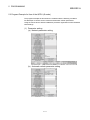
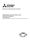
Analog-Digital Converter Module Type AJ65SBT-64AD
,
User s Manual
Mitsubishi Programmable Controller
SAFETY PRECAUTIONS
(Always read these precautions before using this equipment.)
Before using this product, please read this manual and the relevant manuals introduced in this manual
carefully and pay full attention to safety to handle the product correctly.
The precautions given in this manual are concerned with this product. Refer to the user’s manual of the
CPU module to use for a description of the PLC system safety precautions.
In this manual, the safety precautions are ranked as "DANGER" and "CAUTION".
DANGER
Indicates that incorrect handling may cause hazardous conditions,
resulting in death or severe injury.
! CAUTION
Indicates that incorrect handling may cause hazardous conditions,
resulting in medium or slight personal injury or physical damage.
!
Note that the ! CAUTION level may lead to a serious consequence according to the circumstances.
Always follow the precautions of both levels because they are important to personal safety.
Please save this manual to make it accessible when required and always forward it to the end user.
[Design Precautions]
!
DANGER
When there are communication problems with the data link, the data for the master module will
be held.
Configure an interlocking circuit in a sequence program so that the safety of the overall system
is always maintained.
!
CAUTION
Do not bunch the control wires or communication cables with the main circuit or power wires, or
install them close to each other.
They should be installed 100mm (3.9inch) or more from each other.
Not doing so could result in noise that would cause erroneous operation.
A-1
[Installation Precautions]
!
CAUTION
Use the Module in the environment that meets the general specifications contained in this
Manual.
Using the Module outside the range of the general specifications may result in electric shock,
fire or malfunction, or may damage or degrade the module.
Securely fix the module to a DIN rail or with mounting screws, and securely tighten the mounting
screws within the specified torque range.
Undertightening can cause a drop or malfunction.
Overtightening can cause a drop or malfunction due to damage of the screws or module.
Do not touch the conducted area or electric parts of the module.
Doing so may cause module malfunctioning or breakdowns.
[Wiring Precautions]
!
CAUTION
Be sure to shut off all phases of the external power supply used by the system before installation
or wiring.
Not doing so can cause the product to be damaged or malfunction.
Always earth the FG and FG1 terminals to the protective earth conductor.
Not doing so can cause a malfunction.
Be sure to tighten any unused terminal screws within a tightening torque range (42 to 50N.cm).
Failure to do so may cause a short circuit due to contact with a solderless terminal.
Use applicable solderless terminals and tighten them with the specified torque.
If any solderless spade terminal is used, it may be disconnected when the terminal screw comes
loose, resulting in failure.
Wire the module correctly after confirming the rated voltage and terminal layout of the product.
Not doing so can cause a fire or failure.
Tighten the terminal screws within the specified torque range.
Undertightening can cause a short circuit or malfunction.
Overtightening can cause a short circuit or malfunction due to damage of the screws or module.
Ensure that no foreign matter such as chips and wire-offcuts enter the module.
Foreign matter can cause a fire, failure or malfunction.
A-2
[Wiring Precautions]
!
CAUTION
Be sure to fix the wires or cables by ducts or clamps when connecting them to the module.
Failure to do so may cause damage of the module or the cables due to accidental pull or
unintentional shifting of the cables, or malfunctions due to poor contact of the cable.
Do not install the control lines together with the communication cables, or bring them close to
each other. Failure to do so may cause malfunctions due to noise.
When disconnecting the cables from the module, do not hold and pull the cable part.
Disconnect the cables after loosening the screws in the portions connected to the module.
Pulling the cables connected to the module can damage the module and cables or can cause a
malfunction due to a cable connection fault.
[Starting and Maintenance Precautions]
!
CAUTION
Do not touch the terminals while the power is on. Doing so may cause malfunctioning.
Be sure to shut off all phases of the external power supply used by the system before cleaning
or retightening the terminal screws.
Not doing so can cause the module to fail or malfunction.
Undertightening can cause a drop, short circuit or malfunction.
Overtightening can cause a drop, short circuit or malfunction due to damage of the screws or
module.
Never disassemble or modify the module.
This may cause breakdowns, malfunctioning, injury and/or fire.
Do not drop or apply any strong impact to the module. Doing so may damage the module.
Be sure to shut off all phases of the external power supply used by the system before mounting
or dismounting the module to or from the panel.
Not doing so can cause the module to fail or malfunction.
Do not mount/remove the module to/from the base unit or the terminal block more than 50 times
(IEC61131-2-compliant), after the first use of the product.
Before handling the module, always touch grounded metal, etc. to discharge static electricity
from the human body.
Failure to do so may cause the module to fail or malfunction.
[Disposal Precautions]
!
CAUTION
When disposing of this product, treat it as industrial waste.
A-3
REVISIONS
* The manual number is given on the bottom left of the back cover.
Print Date
* Manual Number
Revision
Oct., 2000 SH (NA)-080106-A First printing
Jun., 2003 SH (NA)-080106-B Program example correction
Correction
SAFETY PRECAUTIONS, About Manuals, Conformation to the EMC
Directive and Low Voltage Instruction, About the Generic Terms and
Abbreviations, Chapter 1, Section 2.1, 2.2, 3.1, 3.2, 3.3.5, 3.5.2, 4.1,
4.7.2, Appendix 1
Mar., 2005 SH (NA)-080106-C Addition
Section 2.3
Correction
SAFETY PRECAUTIONS, About Manuals, Section 3.1, 4.2, Appendix 2
Mar., 2006 SH (NA)-080106-D Correction
REVISIONS, Section 2.3
Jan., 2007 SH (NA)-080106-E Correction
SAFETY PRECAUTIONS, Section 4.3, 5.3, Appendix 2
Japanese Manual Version SH-080087-F
This manual confers no industrial property rights or any rights of any other kind, nor does it confer any patent
licenses. Mitsubishi Electric Corporation cannot be held responsible for any problems involving industrial property
rights which may occur as a result of using the contents noted in this manual.
© 2000 MITSUBISHI ELECTRIC CORPORATION
A-4
INTRODUCTION
Thank you for choosing a Mitsubishi MELSEC-A Series General Purpose Programmable Controller.
Before using your new PLC, please read this manual thoroughly to gain an understanding of its functions so
you can use it properly.
CONTENTS
SAFETY PRECAUTIONS..............................................................................................................................AREVISIONS ....................................................................................................................................................AINTRODUCTION............................................................................................................................................AAbout Manuals................................................................................................................................................AConformation to the EMC Directive and Low Voltage Instruction ................................................................AAbout the Generic Terms and Abbreviations ................................................................................................AProduct components ......................................................................................................................................A1. OVERVIEW
1
4
5
7
7
8
9
1- 1 to 1- 2
1.1 Features.................................................................................................................................................... 1- 1
2. SYSTEM CONFIGURATION
2- 1 to 2- 2
2.1 Overall Configuration ............................................................................................................................... 2- 1
2.2 Applicable System.................................................................................................................................... 2- 2
2.3 Checking Hardware Versions .................................................................................................................. 2- 2
3 SPECIFICATION
3- 1 to 3- 16
3.1 General Specification ............................................................................................................................... 3- 1
3.2 Performance Specification ....................................................................................................................... 3- 2
3.3 I/O Conversion Characteristics ................................................................................................................ 3- 3
3.3.1 Voltage input characteristics ............................................................................................................. 3- 4
3.3.2 Current input characteristics ............................................................................................................. 3- 5
3.3.3 Relationship between the offset/gain setting and digital output value............................................. 3- 6
3.3.4 Accuracy ............................................................................................................................................ 3- 6
3.3.5 Conversion speed ............................................................................................................................. 3- 7
3.4 Function List ............................................................................................................................................. 3- 8
3.4.1 Sampling processing......................................................................................................................... 3- 9
3.4.2 Moving average processing .............................................................................................................. 3- 9
3.5 Remote I/O Signals ................................................................................................................................. 3- 10
3.5.1 Remote I/O signal list ....................................................................................................................... 3- 10
3.5.2 Functions of the remote I/O signals ................................................................................................. 3- 11
3.6 Remote Register ..................................................................................................................................... 3- 13
3.6.1 Remote register allocation ............................................................................................................... 3- 13
3.6.2 A/D conversion enable/prohibit specification (Address RWwm) .................................................... 3- 14
3.6.3 Input range setting (Address RWwm+1) ......................................................................................... 3- 15
3.6.4 Moving average processing count setting (Address RWwm+2)..................................................... 3- 16
3.6.5 CH. Digital output value (Address RWrn to RWrn+3)................................................................. 3- 16
A-5
4 SETUP AND PREPARATION BEFORE OPERATION
4- 1 to 4- 10
4.1 Pre-Operation Procedure......................................................................................................................... 4- 1
4.2 Precautions When Handling .................................................................................................................... 4- 1
4.3 Name of Each Part................................................................................................................................... 4- 3
4.4 Offset/Gain Setting................................................................................................................................... 4- 5
4.5 Station Number Setting............................................................................................................................ 4- 7
4.6 Facing Direction of the Module Installation ............................................................................................. 4- 7
4.7 Data Link Cable Wiring ............................................................................................................................ 4- 8
4.7.1 Instructions for handling the CC-Link dedicated cables................................................................... 4- 8
4.7.2 Connection of the CC-Link dedicated cables ................................................................................... 4- 8
4.8 Wiring........................................................................................................................................................ 4- 9
4.8.1 Wiring precautions............................................................................................................................. 4- 9
4.8.2 Module connection example ............................................................................................................. 4- 9
4.9 Maintenance and Inspection.................................................................................................................... 4-10
5 PROGRAMMING
5- 1 to 5- 15
5.1 Programming Procedure.......................................................................................................................... 5- 1
5.2 Conditions of Program Example.............................................................................................................. 5- 2
5.3 Program Example for Use of the QCPU (Q mode)................................................................................. 5- 4
5.4 Program Example for Use of the QnACPU............................................................................................. 5- 8
5.5 Program Example for Use of the ACPU/QCPU (A mode) (dedicated instructions) ............................. 5- 11
5.6 Program Example for Use of the ACPU/QCPU (A mode) (FROM/TO instructions) ............................ 5- 14
6 TROUBLESHOOTING
6- 1 to 6- 6
6.1 Using the Remote Input Signals to Check Errors ................................................................................... 66.2 Using the LED Indications to Check Errors............................................................................................. 66.3 When the digital output value cannot be read......................................................................................... 66.4 Troubleshooting for the Case where the "ERR." LED of the Master Station Flickers ........................... 6APPENDIX
1
2
4
5
Appendix- 1 to Appendix- 4
Appendix 1 Comparison between This Product and Conventional Product ...................................Appendix- 1
Appendix 2 External Dimensions......................................................................................................Appendix- 3
INDEX
Index- 1 to Index- 3
A-6
About Manuals
The following manuals are also related to this product.
In necessary, order them by quoting the details in the tables below.
Related Manuals
Manual Number
(Model Code)
Manual Name
CC-Link System Master/Local Module User's Manual Type AJ61BT11/A1SJ61BT11
Describes the system configuration, performance specifications, functions, handling, wiring and
troubleshooting of the AJ61BT11 and A1SJ61BT11.
(Optionally available)
CC-Link System Master/Local Module User's Manual Type AJ61QBT11/A1SJ61QBT11
Describes the system configuration, performance specifications, functions, handling, wiring and
troubleshooting of the AJ61QBT11 and A1SJ61QBT11.
(Optionally available)
CC-Link System Master/Local Module User's Manual QJ61BT11N
Describes the system configuration, performance specifications, functions, handling, wiring and
troubleshooting of the QJ61BT11N.
(Optionally available)
type AnSHCPU/AnACPU/AnUCPU/QCPU-A (A Mode) (Dedicated Instructions)
Programming Manual
Explains the instructions extended for the AnSHCPU/AnACPU/AnUCPU/QCPU-A (A Mode).
(Optionally available)
IB-66721
(13J872)
IB-66722
(13J873)
SH-080394E
(13JR64)
IB-66251
(13J742)
Conformation to the EMC Directive and Low Voltage Instruction
When complying with EMC Directives and Low-Voltage Directives by assembling a
Mitsubishi PLC compatible with EMC Directive and Low-Voltage Directives into the
user product, refer to Chapter 3 "EMC Directives and Low-Voltage Directives" in the
User’s Manual (Hardware) for the CPU module being used.
The CE logo is printed on the rating plate on the main body of the PLC that conforms
to the EMC directive and low voltage instruction.
To conform this product to the EMC Directive and Low Voltage Directive, refer to the
Section of "CC-Link Modules" in Chapter 3 "EMC Directive and Low Voltage
Directive" of the User's Manual (Hardware) of the CPU module used.
A-7
About the Generic Terms and Abbreviations
Unless otherwise specified, the following generic terms and abbreviations are used
in this manual to describe Type AJ65SBT-64AD analog-digital converter module.
Generic Term/Abbreviation
GX Developer
ACPU
QnACPU
QCPU (A mode)
QCPU (Q mode)
Master station
Local station
Remote I/O station
Remote device station
Remote station
Intelligent device station
Master module
SB
SW
RX
RY
RWw
RWr
Description
Generic product name of the product types SWnD5C-GPPW-E, SWnD5C-GPPW-EA,
SWnD5C-GPPW-EV and SWnD5C-GPPW-EVA
(n in the type indicates 4 or more.)
Generic term for A0J2CPU, A0J2HCPU, A2CPU, A2CPU-S1, A3CPU, A1SCPU,
A1SCPU-S1, A1SCPUC-24-R2, A1SHCPU, A1SJCPU, A1SJCPU-S3, A1SJHCPU,
A1NCPU, A2NCPU, A2NCPU-S1, A3NCPU, A3MCPU, A3HCPU, A2SCPU,
A2SCPU-S1, A2SHCPU, A2SHCPU-S1, A2ACPU, A2ACPU-S1, A3ACPU, A2UCPU,
A2UCPU-S1, A2ASCPU, A2ASCPU-S1, A2ASCPU-S30, A2USHCPU-S1, A3UCPU,
A4UCPU
Generic term for Q2ACPU, Q2ACPU-S1, Q2ASCPU, Q2ASCPU-S1, Q2ASHCPU,
Q2ASHCPU-S1, Q3ACPU, Q4ACPU, Q4ARCPU
Generic term for Q02CPU-A, Q02HCPU-A, Q06HCPU-A
Generic term for Q00JCPU, Q00CPU, Q01CPU, Q02CPU, Q02HCPU, Q06HCPU,
Q12HCPU, Q25HCPU, Q12PHCPU, Q25PHCPU
Station that controls the data link system.
One master station is required for each system.
Station having a PLC CPU and the ability to communicate with the master and other
local stations.
Remote station that handles bit unit data only. (Performs input and output with
external devices.) (AJ65BTB1-16D, AJ65SBTB1-16D)
Remote station that handles bit unit and word unit data only. (Performs input and
output with external devices, and analog data exchange.)
Generic term for remote I/O station and remote device station.
(Controlled by the master station)
Station that can perform transient transmission, such as the AJ65BT-R2 (including
local stations).
Generic term for QJ61BT11N, QJ61BT11, AJ61BT11, A1SJ61BT11, AJ61QBT11,
and A1SJ61QBT11 when they are used as master stations.
Link special relay (for CC-Link)
Bit unit information that indicates the module operating status and data link status of
the master station/local station. (Expressed as SB for convenience)
Link special register (for CC-Link)
16 bit unit information that indicates the module operating status and data link status
of the master station/local station. (Expressed as SW for convenience)
Remote input (for CC-Link)
Information entered in bit units from the remote station to the master station.
(Expressed as RX for convenience)
Remote output (for CC-Link)
Information output in bit units from the master station to the remote station.
(Expressed as RY for convenience)
Remote register (Write area for CC-Link)
Information output in 16-bit units from the master station to the remote device station.
(Expressed as RWw for convenience)
Remote register (Read area for CC-Link)
Information entered in 16-bit units from the remote device station to the master
station.
(Expressed as RWr for convenience)
A-8
Product components
This product consists of the following.
Product Name
Quantity
Type AJ65SBT-64AD analog-digital converter module
Type AJ65SBT-64AD analog-digital converter module user's manual (hardware)
A-9
1
1
1 OVERVIEW
MELSEC-A
1 OVERVIEW
1
This user's manual explains the specifications, handling, programming methods and
others of Type AJ65SBT-64AD analog-digital converter module (hereafter abbreviated
to the "AJ65SBT-64AD") which is used as a remote device station of a CC-Link system.
The AJ65SBT-64AD converts the analog signals (voltage or current input) from the
PLC's external source to a 16-bit encoded binary data digital value.
1.1 Features
This section gives the features of the AJ65SBT-64AD.
(1) High accuracy
This module performs A/D conversion at the accuracy of ±0.4% relative to the
maximum value of the digital output value at the operating ambient temperature
of 0 to 55°C, or at ±0.2% relative to the maximum value of the digital output value
at the operating ambient temperature of 25±5°C.
(2) Input range selectable per channel
You can choose the analog input range per channel to change the I/O conversion
characteristics.
(3) High resolution of 1/±4000
By changing the input range, you can choose and set the digital value resolution
to either 1/4000 or 1/±4000 (when the -10 to +10V range or user range setting 1
is selected) to provide high-resolution digital values.
(4) Designation of sampling processing or moving average processing
As a conversion method, you can specify sampling processing or moving
average processing per channel.
(5) Smaller than the conventional A/D converter module
This module is 60% smaller in installation area and 38% less in volume than the
conventional CC-Link A/D converter module (AJ65BT-64AD).
(6) Up to 42 modules connectable
You can connect up to 42 AJ65SBT-64AD modules to one master station.
1-1
1 OVERVIEW
MELSEC-A
MEMO
1
1-2
2 SYSTEM CONFIGURATION
MELSEC-A
2 SYSTEM CONFIGURATION
This chapter describes the system configuration for use of the AJ65SBT-64AD.
2.1 Overall Configuration
2
The overall configuration for use of the AJ65SBT-64AD is shown below.
CC-Link master/local module (master station)
(AJ61BT11, A1SJ61BT11, AJ61QBT11,
A1SJ61QBT11, QJ61BT11, QJ61BT11N)
CC-Link master/local module (local station)
(AJ61BT11, A1SJ61BT11, AJ61QBT11, A1SJ61QBT11,
QJ61BT11, QJ61BT11N)
CC-Link dedicated cable
(Intelligent device station)
AJ65SBT-64AD
(Remote device station)
(Remote I/O station)
(Remote device station)
1 station occupied
RX/RY: 32 points each
RWr/RWw: 4 points each
Object whose
voltage/current
will be detected
2-1
2 SYSTEM CONFIGURATION
MELSEC-A
2.2 Applicable System
This section explains the applicable system.
(1) Applicable master modules
The following master modules can be used with the AJ65SBT-64AD.
AJ61BT11
A1SJ61BT11
AJ61QBT11
A1SJ61QBT11
QJ61BT11
QJ61BT11N
(2) Restrictions on use of CC-Link dedicated instructions (RLPA,
RRPA)
The CC-Link dedicated instructions may not be used depending on the PLC CPU
and master module used.
For details of the restrictions, refer to the A series master module user's manual,
and the Programing Manual type AnSHCPU/AnACPU/AnUCPU/QCPU (A mode)
(Dedicated Instructions).
This module does not allow the use of the dedicated instructions other than
RLPA and RRPA.
Refer to Section 5.5 for a program example using the dedicated instructions
(RLPA, RRPA).
2.3 Checking Hardware Versions
The hardware versions of the AJ65SBT-64AD can be checked on the DATE section on
the rating plate, which is situated on the side of the module.
Year and month of manufacture
MODEL
Hardware version
Software version
POWER
DATE
Conformed standard
yymm A B
MADE IN JAPAN
BD992C154H06
2-2
2
3 SPECIFICATION
MELSEC-A
3 SPECIFICATION
This chapter provides the specifications of the AJ65SBT-64AD.
3.1 General Specification
Table 3.1 indicates the general specifications of the AJ65SBT-64AD.
Table 3.1 General specification
3
Item
Specification
Usage ambient temperature
0 to 55°C
Storage ambient temperature
-20 to 75°C
Usage ambient humidity
10 to 90%RH, no condensation
Storage ambient humidity
10 to 90%RH, no condensation
When there is intermittent vibration
Conforming to JIS B
3502, IEC 61131-2
Vibration durability
Frequency
Acceleration
Amplitude
10 to 57Hz
—
0.075mm (0.0030inch)
57 to 150Hz
9.8m/s2
—
When there is continuous vibration
Frequency
Acceleration
Amplitude
10 to 57Hz
—
0.035mm (0.0014inch)
57 to 150Hz
4.9m/s2
Sweep count
10 times in each
direction X, Y, Z
(80 minutes)
—
2
Shock durability
Conforming to JIS B 3502, IEC 61131-2 (147m/s , 3 times each in 3 directions)
Usage environment
No corrosive gas
3
Usage height *
Less than 2000m (less than 6562ft.)
Installation area
Within the control board
1
Over-voltage category *
Less than II
Pollution level *2
Less than 2
*1 Indicates the location where the device is connected from the public cable network to the device structure wiring
area.
Category II applies to the devices to which the power is supplied from a fixed equipment.
Surge withstand voltage for devices with up to 300V of rated voltage is 2500V.
*2 This is an index which indicates the degree of conductive object generation in the environment Pollution level 2 is
when only non-conductive pollution occurs.
A temporary conductivity caused by condensation must be expected occasionally.
*3 Do not operate or store the PLC in the environment where the pressure applied is equal to greater than the
atmospheric pressure at the altitude of 0m.
Doing so may cause a malfunction. Please consult our branch office when the PLC is to be operated under pressure.
3-1
3 SPECIFICATION
MELSEC-A
3.2 Performance Specification
Table 3.2 indicates the performance specifications of the AJ65SBT-64AD.
Table 3.2 Performance specification
Item
Analog input
Specification
Voltage
-10 to +10V DC (input resistance 1M )
Current
0 to +20mA DC (input resistance 250 )
Digital output
16-bit signed binary (-4096 to +4095)
Accuracy
Analog input range
Voltage
I/O characteristics, maximum
resolution, accuracy (accuracy
relative to maximum value of digital
output value)
Current
Digital output
-10 to +10V
User range setting 1 -4000 to +4000
(-10 to +10V)
0 to 5V
1 to 5V
0 to 4000
User range setting 2
(0 to 5V)
0 to 20mA
4 to 20mA
User range setting 3
(0 to 20mA)
0 to 4000
Ambient
temperature
0 to 55°C
Max.
Ambient
temperature Resolution
25±5°C
2.5mV
1.25mV
±0.4%
(±16 digit*)
±0.2%
(±8 digit*)
1.0mV
5µA
4µA
* : digit indicates digital value.
Factory setting is -10 to +10V.
Maximum conversion speed
Absolute maximum input
Analog input points
CC-Link station type
Number of occupied stations
Communication cable
Dielectric withstand voltage
Isolation system
Noise immunity
External
connection
Communication area,
module power supply
I/O area
Applicable wire size
Applicable solderless terminals
Module mounting screw
Supported DIN rail
External supply power
Weight
1ms/channel
Voltage ±15 V, current ±30mA
4 channels/1module
Remote device station
1 station (RX/RY: 32 points each, RWr/RWw: 4 points each)
CC-Link dedicated cable
Between power supply/communication system batch and analog input batch: 500VAC, 1 minute
Across communication system terminals and all analog input terminals: Photocoupler isolated
Across power supply system terminals and all analog input terminals: Photocoupler isolated
Across channels: Non-isolated
By noise simulator of 500Vp-p noise voltage, 1µs noise width and 25 to 60Hz noise frequency
7-point 2-piece terminal block [transmission circuit, module power supply, FG]
M3 5.2 Tightening torque: 59 to 88N·cm
Applicable solderless terminals: 2 max.
Direct-coupled, 18-point terminal block [analog input area]
M3 5.2 Tightening torque: 59 to 88N·cm
Applicable solderless terminals: 2 max.
0.3 to 0.75mm2
RAV1.25-3 (conforming to JIS C 2805)
[Applicable wire size: 0.3 to 1.25mm2]
V2-MS3, RAP2-3SL, TGV2-3N
[Applicable wire size: 1.25 to 2.0mm2]
M4 screw
0.7mm
16mm or more (tightening torque range: 78 to 108N cm)
Can also be mounted to DIN rail
TH35-7.5Fe, TH35-7.5Al (conforming to IEC 60715)
24V DC (20.4 to 26.4V DC)
Inrush current: 8.5A, within 2.3ms
Current consumption: 0.090A
0.20kg
3-2
3
3 SPECIFICATION
MELSEC-A
3.3 I/O Conversion Characteristics
The I/O characteristics is the slope created by connecting the offset and gain values,
with a straight line when converting the analog signals (voltage or current input) from
an external source of the PLC to digital values.
The offset value is an analog input value (voltage or current) at which the digital output
value is 0.
The gain value is an analog input value (voltage or current) at which the digital output
value is 4000.
3-3
3 SPECIFICATION
MELSEC-A
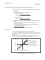
3.3.1 Voltage input characteristics
The voltage input characteristic graph is shown below.
Analog input parcitcal value
4095
4000
Digital output value
1
2000
2
3
0
-96
1
-2000
-4000
-4096
-15
-10
-5
0
5
Analog input voltage (V)
Number
Analog Input Range Setting
1)
2)
3)
—
—
-10 to +10V
0 to 5V
1 to 5V
User range setting 1 (-10 to +10V)
User range setting 2 (0 to 5V)
Offset
Value
0V
0V
1V
0V
0V
Gain
Value
10V
5V
5V
10V
5V
10
15
Digital Output
Value*
-4000 to +4000
0 to 4000
-4000 to +4000
0 to 4000
Maximum
Resolution
2.5mV
1.25mV
1.0mV
2.5mV
1.0mV
Fig. 3.1 Voltage Input Characteristic
POINT
(1) Do not input more than ±15V. The element may be damaged.
(2) If the analog input provided corresponds to the digital output value* beyond its
range, the digital output value is fixed to the maximum or minimum.
For 0 to 4000, the digital output value is within the range -96 to 4095.
For -4000 to +4000, the digital output value is within the range -4096 to +4095.
(3) Within the analog input and digital output scopes of each input range, the
maximum resolution and accuracy are within the performance specification
range. Outside those scopes, however, they may not fall within the performance
specification range. (Avoid using the dotted line part in Fig. 3.1.)
(4) Set the offset and gain values of the user range setting within the range
satisfying the following conditions.
(a) Setting range when user range setting 1 is selected: -10 to +10V
(b) Setting range when user range setting 2 is selected: 0 to 5V
(c) (Gain value) > (Offset value)
If you attempt to make setting outside the setting range of (a) or (b), the "RUN"
LED flickers at 0.5s intervals.
Set the values within the setting range.
If you attempt to make setting outside the setting range of (c), the "RUN" LED
flickers at 0.5s intervals.
Make setting again.
3-4
3 SPECIFICATION
MELSEC-A
3.3.2 Current input characteristics
The current input characteristic graph is shown below.
Analog input
parcitcal value
4095
4000
Digital output value
2
2000
1
0
-96
4
-2000
-4000
-30
-20
-10
0
10
Analog input current (mA)
Number
Analog Input Range Setting
1)
2)
—
0 to 20mA
4 to 20mA
User range setting 3 (0 to 20mA)
Offset
Value
0mA
4mA
0mA
Gain
Value
20mA
20mA
20mA
20
30
Digital Output
Value*
0 to 4000
Maximum
Resolution
5µA
4µA
Fig. 3.2 Current Input Characteristic
POINT
(1) Do not input more than ±30mA. A breakdown may result due to heat increase.
(2) If the analog input provided corresponds to the digital output value* beyond its
range, the digital output value is fixed to the maximum or minimum.
For 0 to 4000, the digital output value is within the range -96 to 4095.
(3) Within the analog input and digital output scopes of each input range, the
maximum resolution and accuracy are within the performance specification
range. Outside those scopes, however, they may not fall within the performance
specification range. (Avoid using the dotted line part in Fig. 3.2.)
(4) Set the offset and gain values of the user range setting within the range
satisfying the following conditions.
(a) Setting range when user range setting 3 is selected: 0 to 20mA
(b) (Gain value) > (Offset value)
If you attempt to make setting outside the setting range of (a), the "RUN" LED
flickers at 0.5s intervals.
Set the values within the setting range.
If you attempt to make setting outside the setting range of (b), the "RUN" LED
flickers at 0.5s intervals.
Make setting again.
3-5
3 SPECIFICATION
MELSEC-A
3.3.3 Relationship between the offset/gain setting and digital output value
The relationship between the offset/gain setting and digital output value is described.
(1) Resolution
The resolution is obtained by the following formula:
(a) For the voltage input:
Resolution =
(Gain value) - (Offset value)
4000
(b) For the current input:
Resolution =
(Gain value) - (Offset value)
4000
(2) Relationship between the maximum resolution and digital output
value
The maximum resolution of the AJ65SBT-64AD is as indicated in the
performance specification.
If the following is satisfied from the offset/gain setting, the digital output value
does not increases /decreases by one.
(Gain value) - (Offset value)
4000
< Maximum resolution
3.3.4 Accuracy
Accuracy is relative to the maximum value of the digital output value.
If you change the offset/gain setting or input range to change the input characteristic,
accuracy does not change and is held within the range indicated in the performance
specifications.
Accuracy is within ±0.2% (±8 digit) at the operating ambient temperature of 25±5°C or
within ±0.4% (±16 digit) at the operating ambient temperature of 0 to 55°C.
Digital output value
4000
Varies within the range of
±0.2% (±8 digit) at operating
ambient temperature of 25±5
Varies within the range of
±0.4% (±16 digit) at operating
ambient temperature of 0 to 55
0
-4000
-10V
0V
Analog input value
10V
Fig. 3.3 Voltage Input Characteristic Accuracy
3-6
.
.
3 SPECIFICATION
MELSEC-A
4000
Digital output value
Varies within the range of
±0.2% (±8 digit) at operating
ambient temperature of 25±5
Varies within the range of
±0.4% (±16 digit) at operating
ambient temperature of 0 to 55
.
.
0
0
20mA
Analog input value
Fig. 3.4 Current Input Characteristic Accuracy
3.3.5 Conversion speed
Conversion speed indicates time from channel changing to A/D conversion completion.
Conversion speed per channel of the AJ65SBT-64AD is 1ms.
Due to the data link processing time of the CC-Link system, there is a transmission
delay until the A/D conversion value is read actually.
For the data link processing time, refer to the user's manual of the master module used.
Example) Data link processing time taken in the asynchronous mode when the master
module is the QJ61BT11 (normal value)
[Calculation expression]
SM+LS×1+remote device station processing time
SM: Scan time of master station sequence program
LS : Link scan time
Remote device station processing time: (Number of channels used+1*) × 1ms
*: Internal processing time of AJ65SBT-64AD
3-7
3 SPECIFICATION
MELSEC-A
3.4 Function List
The AJ65SBT-64AD function list is shown in table 3.3.
Table 3.3 AJ65SBT-64AD function list
Item
Description
Reference section
Sampling processing
Perform A/D conversion of an analog input value one by one and store the result into the
remote register each time.
Section 3.4.1
Section 3.5.2
Moving average
processing
Average the digital output values of the specified count measured per sampling time.
Section 3.4.2
Section 3.5.2
Section 3.6.4
A/D conversion
enable/prohibit
specification
Specify whether A/D conversion is enabled or disabled per channel.
By prohibiting the conversion for the channels which are not used, the sampling time can
be shortened.
Section 3.6.2
Can set the analog input range per channel to change the I/O conversion characteristics.
Select the input range setting from among the following 8 types.
Input range changing
function
Offset/gain setting
Input Range
Set Value
-10 to +10V
0H
0 to 5V
1H
1 to 5V
2H
0 to 20mA
3H
4 to 20mA
4H
User range setting 1 (-10 to +10V)
5H
User range setting 2 (0 to 5V)
6H
User range setting 3 (0 to 20mA)
7H
The offset/gain setting can be performed volumeless for each channel, and the I/O
conversion characteristics can be changed.
3-8
Section 3.6.3
Section 4.4
3 SPECIFICATION
MELSEC-A
3.4.1 Sampling processing
The A/D conversion is performed successively for the analog input, and the converted
digital output values are stored in the remote register.
The processing time to store the digital output value into the remote register after the
sampling processing differs depending on the number of A/D conversion enabled
channels.
(Processing time)
Number of A/D conversion enabled channels) 1 (ms)
Maximum conversion speed
[Example] When three channels, channels 1, 2, and 3 are enabled for conversion:
3×1 = 3 (ms)
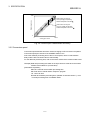
3.4.2 Moving average processing
The specified count of digital output values imported per sampling time are averaged to
find a value, which is then stored into the remote register.
Since average processing is performed with data shifted per sampling, the most recent
digital output value is available.
Average processing can be performed without changing the conversion speed.
Use moving average processing count setting (address RWwm+2) to set the number
of moving average processings.
The count can be selected from among four types: 4, 8, 16 and 32 times.
Moving average processing at the count setting of 4 times
Sampling time
A/D conversion value
4000
3
2
4
5
6
1
7
8
9
12
10
11
Remote register
2000
Stored first time
Stored second time
Stored third time
0
A/D conversion completion flag ON
Time [ms]
Data transition inside remote register
Stored first time
Stored second time
Stored third time
1+2+3+4
2+3+4+5
3+4+5+6
4
4
4
3-9
Digital output value
3 SPECIFICATION
MELSEC-A
3.5 Remote I/O Signals
This section describes the assignment and functions of the remote I/O signals.
3.5.1 Remote I/O signal list
Remote inputs (RX) mean the input signals from the AJ65SBT-64AD to the master
module, and remote outputs (RY) mean the output signals from the master module to
the AJ65SBT-64AD.
In communications with the master station, the AJ65SBT-64AD uses 32 points of the
remote inputs (RX) and 32 points of the remote outputs (RY). Table 3.4 indicates the
assignment and names of the remote I/O signals.
Table 3.4 Remote I/O Signals List
Signal direction: AJ65SBT-64AD
Master Module
Signal direction: Master Module
AJ65SBT-64AD
Remote input (RX)
Signal name
Remote output (RY)
Signal name
RXn0
CH.1 A/D conversion completion flag
RYn0
CH.1 moving average processing specifying flag
RXn1
CH.2 A/D conversion completion flag
RYn1
CH.2 moving average processing specifying flag
RXn2
CH.3 A/D conversion completion flag
RYn2
CH.3 moving average processing specifying flag
RXn3
CH.4 A/D conversion completion flag
RYn3
CH.4 moving average processing specifying flag
RXn4
CH.1 range error flag
RXn5
CH.2 range error flag
RXn6
CH.3 range error flag
RXn7
CH.4 range error flag
RXn8
to
RXnB
Reserved
RXnC
E PROM write error flag
RYn4
to
RY(n+1)7
Reserved
RY(n+1)8
Initial data processing completion flag
RXnD
RXnE
2
Reserved
RXnF
Test mode flag
RX(n+1)0
to
RX(n+1)7
Reserved
RX(n+1)8
Initial data processing request flag
RX(n+1)9
Initial data setting completion flag
RY(n+1)9
Initial data setting request flag
RX(n+1)A
Error status flag
RY(n+1)A
Error reset request flag
RX(n+1)B
Remote READY
RX(n+1)C
to
RX(n+1)F
Reserved
RY(n+1)B
to
RY(n+1)F
Reserved
POINT
The reserved devices given in Table 3.4 are used by the system and cannot be
used by the user.
If the user has used (turned on/off) any of them, we cannot guarantee the functions
of the AJ65SBT-64AD.
3 - 10
3 SPECIFICATION
MELSEC-A
3.5.2 Functions of the remote I/O signals
Table 3.5 explains the functions of the remote I/O signals of the AJ65SBT-64AD.
Table 3.5 Remote I/O Signal Details (1/2)
Device No.
Signal Name
Description
RXn0
to
RXn3
CH. A/D Conversion
completion flag
The A/D conversion completion flag turns on at completion of the A/D conversion of
the corresponding channel when the initial data setting request flag (RY(n+1)9) turns
from off to on after power-on.
The A/D conversion completion flag processing is processed only once when the A/D
conversion enable/prohibit specification is changed.
When changing the A/D conversion from prohibit to enable:
When the average processing is specified, the flag turns on after completing the
average processing of the number of times or time, and storing the A/D conversion
digital value in the remote register.
When changing the A/D conversion from enable to prohibit:
The corresponding channel's A/D conversion completion flag turns off.
RXn4
to
RXn7
CH.
Turns on when the value set for input range setting is outside the setting range.
Turns on if all channels are not set to any of "user range settings 1 to 3" at offset/gain
setting (in the test mode).
range error flag
2
RXnC
E PROM write error flag
RXnF
Test mode flag
Turns on if the number of E2PROM write times exceeds its limit (100,000 times per
channel). If this flag has turned on, this module itself has failed (hardware fault) and
therefore this flag cannot be reset (turned off) by the error reset request flag.
Turns on in the test mode.
(Used for interlock to prevent wrong output during offset/gain setting.)
After power-on, the initial data processing request flag is turned on by the AJ65SBT64AD to request the initial data to be set.
Also, after the initial data processing is complete (initial data processing completion
flag RY(n+1)8 ON), the flag is turned off.
RX(n+1)8
Initial data processing request flag
RY(n+1)8
Initial data processing completion flag
RX(n+1)8
Initial data processing
request flag
RX(n+1)9
Initial data setting completion flag
RY(n+1)9
Initial data setting request flag
RX(n+1)B
Remote ready
CH.
RXn0 to RXn3
A/D conversion completion flag
: Performed by sequence ladder
: Performed by AJ65SBT-64AD
RX(n+1)9
Initial data setting completion
flag
When the initial data setting request (RY(n+1)9 ON) is made, the flag turns on after
the initial data setting completion is done.
Also, after the initial data setting is complete, the initial data setting completion flag
turns off when the initial data setting request flag turns off.
n: Address allocated to the master module by the station number setting.
3 - 11
3 SPECIFICATION
MELSEC-A
Table 3.5 Remote I/O Signal Details (2/2)
Device No.
Signal Name
Description
Turns on when CH.
range error flag (RXn4 to RXn7) or E2PROM write error flag
(RXnC) has turned on.
Does not turn on at occurrence of the watchdog timer error. ("RUN" LED goes off.)
RX(n+1)A
Error status flag
RX(n+1)A
Error status flag
RXn4 to RXn7
CH. range error flag
RY(n+1)A
Error reset request flag
: Performed by sequence ladder
: Performed by AJ65SBT-64AD
Remote READY
Turns on when initial data setting is completed after power-on or at termination of the
test mode.
(Used for interlocking read/write from/to the master module.)
CH. moving average
processing specifying flag
Set the A/D conversion system to sampling processing or moving average
processing per channel.
Made valid on the leading edge of the initial data setting request flag (RY(n+1)9).
OFF: Sampling processing
ON: Moving average processing
RY(n+1)8
Initial data processing
completion flag
Turns on after initial data processing completion when initial data processing is
requested after power-on or test mode operation.
RY(n+1)9
Initial data setting request
flag
Turns on at the time of initial data setting or changing.
RY(n+1)A
Error reset request flag
RX(n+1)B
RYn0
to
RYn3
When this flag turns on, the CH. range error flag (RXn4 to RXn7) is reset (turned
off) and the error status flag (RX(n+1)A) is also reset, but the E2PROM write error
flag (RXnC) cannot be rest and therefore the error status flag remains on.
n: Address allocated to the master module by the station number setting.
3 - 12
3 SPECIFICATION
MELSEC-A
3.6 Remote Register
The AJ65SBT-64AD has a remote resister for data communication with the master
module. The remote register allocation and data structures are described.
3.6.1 Remote register allocation
The remote register allocation is shown in Table 3.6.
Table 3.6 Remote register allocation
Communication direction
Master
Remote
Remote
Master
Address
Description
Default value
Reference section
RWwm
A/D conversion enable/prohibit specification
0
Section 3.6.2
RWwm+1
Input range setting
0
Section 3.6.3
RWwm+2
Moving average processing count setting
0
Section 3.6.4
RWwm+3
Reserved
0
——
RWrn
CH.1 digital output value
0
RWrn+1
CH.2 digital output value
0
RWrn+2
CH.3 digital output value
0
RWrn+3
CH.4 digital output value
0
Section 3.6.5
m, n: Address allocated to the master module by the station number setting.
POINT
Do not read or write data from or to the reserved area of the remote register. If data
is read or written, we cannot guarantee the functions of the AJ65SBT-64AD.
3 - 13
3 SPECIFICATION
MELSEC-A
3.6.2 A/D conversion enable/prohibit specification (Address RWwm)
(1) Set whether A/D conversion is enabled or disabled per channel.
(2) By setting the unused channels to conversion prohibit, the sampling cycle can be
shortened.
Example) The sampling cycle when only channels 1 and 3 are set to A/D
conversion enabled:
2 (Number of channels enabled) × 1ms (Conversion speed at one channel) = 2ms
(3) Operation is performed according to the setting made for the leading edges of
initial data setting request flag (RY(n+1)9).
(4) The default setting is A/D conversion disable for all channels.
b15
b14
b13
b12
b11
b10
b9
b8
b7
b6
b5
b4
b3
b2
b1
b0
CH.4 CH.3 CH.2 CH.1
Ignored
3 - 14
1: Enable A/D conversion
0: Prohibit A/D conversion
3 SPECIFICATION
MELSEC-A
3.6.3 Input range setting (Address RWwm+1)
(1) Set the analog input range per channel.
(2) Operation is performed according to the setting made for the leading edges of the
initial data setting request flag (RY(n+1)9).
(3) The default setting is -10 to +10V for all channels.
b15
to
b12
b11
to
CH.4
CH.3
b8
b7
to
b4
b3
CH.2
to
b0
CH.1
Input Range
Set Value
-10 to +10V
0H
0 to 5V
1H
1 to 5V
2H
0 to 20mA
3H
4 to 20mA
4H
User range setting 1 (-10 to +10V)
5H
User range setting 2 (0 to 5V)
6H
User range setting 3 (0 to 20mA)
7H
(4) When making offset/gain setting, set all channels to any of "user range settings 1
to 3".
Setting any other range will result in an error and flicker the "RUN" LED at 0.1s
intervals.
3 - 15
3 SPECIFICATION
MELSEC-A
3.6.4 Moving average processing count setting (Address RWwm+2)
(1) Set the average processing count of the channel for which moving average
processing has been specified in the CH.
moving average processing
specifying flag (RYn0 to RYn3).
(2) Sampling processing is performed for the channel whose CH.
moving average
processing specifying flag (RYn0 to RYn3) was not turned on, independently of
the moving average processing count setting.
(3) Operation is performed according to the setting made for the leading edges of the
initial data setting request flag (RY(n+1)9).
(4) The default setting is 4 times for all channels.
Bits b2, b3, b6, b7, b10, b11, b14 and b15 are ignored.
b15
b14 b13
b12
b11
b10 b9
CH.4
b6
CH.3
Ignored
3.6.5 CH.
b8 b7
Ignored
b5
b4
b3
b2
CH.2
b1
b0
CH.1
Ignored
Ignored
Set Count
Set Value
4 times
0H
8 times
1H
16 times
2H
32 times
3H
Digital output value (Address RWrn to RWrn+3)
(1) The digital value after the A/D conversion is stored in the remote register address
from RWrn to RWrn+3 for each channel.
(2) The digital output value is expressed in a 16-bit encoded binary.
b15 b14 b13 b12 b11 b10 b9 b8 b7 b6 b5 b4 b3 b2 b1 b0
Date section
b12 to b14 change to 1 when the sign is negative
(1 at b15) and to 0 when it is positive (0 at b15).
(A negative digital value is expressed in 2's complement.)
Sign bit
1: Negative
0: Positive
3 - 16
4 SETUP AND PREPARATION BEFORE OPERATION
MELSEC-A
4 SETUP AND PREPARATION BEFORE OPERATION
4.1 Pre-Operation Procedure
This section explains the preparatory procedure for operating the AJ65SBT-64AD.
START
Create a program.
(When making offset/gain setting, set all
channels to any of user range settings 1 to 3
in the sequence program.)
4
.......Refer to Chapter 5.
No
Make offset/gain setting?
Yes
Start data link.
Offset/gain setting (Refer to Section 4.4.)
END
4.2 Precautions When Handling
The precautions when handling the AJ65SBT-64AD are described below:
CAUTION
Do not touch the terminals while power is on. Doing so can cause a malfunction.
Ensure that no foreign matter such as chips and wire-offcuts enter the module.
Foreign matter can cause a fire, failure or malfunction.
Do not disassemble or modify the module.
Doing so can cause a failure, malfunction, injury or fire.
Do not touch the conductive and electronic parts of the module directly.
Doing so can cause the module to malfunction or fail.
Do not drop or apply any strong impact to the module.
Doing so may damage the module.
Do not touch the conductive parts of the module directly.
Doing so can cause the module to malfunction or fail.
Tighten the terminal screws within the specified torque range.
Undertightening can cause a short circuit or malfunction.
Overtightening can cause a short circuit or malfunction due to damage of the
screws or module.
Dispose of the product as industrial waste.
4-1
4 SETUP AND PREPARATION BEFORE OPERATION
CAUTION
MELSEC-A
Use the module in the environment indicated in the general specifications given in
this manual.
Not doing so can cause an electric shock, fire, malfunction, product damage or
deterioration.
Securely fix the module to a DIN rail or with mounting screws, and securely tighten
the mounting screws within the specified torque range.
Undertightening can cause a drop or malfunction.
Overtightening can cause a drop or malfunction due to damage of the screws or
module.
Be sure to shut off all phases of the external power supply used by the system
before mounting or dismounting the module to or from the panel.
Not doing so can cause the module to fail or malfunction.
Mounting/removing the terminal block is limited to 50 times after using a product.
(IEC 61131-2-compliant)
Before handling the module, always touch grounded metal, etc. to discharge static
electricity from the human body.
Failure to do so may cause the module to fail or malfunction.
(1) Perform the tightening of the module installation screws and terminal screws in the
following range.
Screw Location
Tightening Torque Range
Module mounting screw (M4 screw)
78 to 108N cm
Terminal block terminal screw (M3 screw)
59 to 88N cm
Terminal block mounting screw (M3.5 screw)
68 to 98N cm
(2) A protective film is attached on the module’s surface for the purpose of scratch
prevention during transportation.
Prior to use, be sure to remove it.
(3) When using the DIN rail adapter, install the DIN rail by making sure of the
following:
(a) Applicable DIN rail models (conforming to the IEC 60715)
TH35-7.5Fe
TH35-7.5Al
(b) DIN rail installation screw interval
When installing the DIN rail, tighten the screws with less than 200mm (7.87
inch) pitches.
(4) When mounting the AJ65SBT-64AD to the DIN rail, press with your finger the
centerline of the DIN rail hook at the bottom of the module until it clicks.
DIN rail
DIN rail hook
(5) Refer to the Master Module user's manual for the name, specification, and
manufacturers of supported cables for the use with AJ65SBT-64AD.
4-2
4
4 SETUP AND PREPARATION BEFORE OPERATION
MELSEC-A
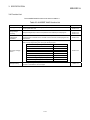
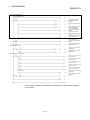
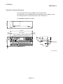
4.3 Name of Each Part
The name of each part in the AJ65SBT-64AD is shown.
1)
PW
2)
RUN L RUN L ERR. CH1 2
3
4
MITSUBISHI
4)
3)
OFFSET GAIN
STATION NO.
B RATE
40 20 10 8 4 2 1 4 2 1
SELECT
AJ65SBT-64AD
DA DG +24V 24G
DB SLD
(FG)
5)
ON
SET
CH1
CH2
CH3
CH4
TEST V+
I+
V+
I+
COM SLD COM AG
(FG1)
TEST COM SLD COM V+
V+
I+
I+
2-piece
(CC-Link
communication
section)
Direct-coupled
(Analog I/O section)
6)
7)
[Terminal numbers and signal names]
1
3
DG
2
4
DB
Number
5
DA
7
+24V
8
24G
6
SLD
10
TEST
12
V+
9
(FG)
11
TEST
13
COM
16
V+
SLD
18
I+
15
COM
Name and
appearance
17
V+
20
22
24
COM
SLD
COM
19
21
23
I+
V+
AG
25
I+
FG1
Description
PW LED
ON : Power supply on
OFF: Power supply off
Normal mode
On
: Normal operation
Flashing : 0.1s intervals indicate an input range error.
Off
: 24VDC power supply shutoff or watchdog timer error occurred.
Test mode
On
: Indicates that the SELECT/SET switch is in the SET position.
Flashing : 0.1s intervals indicate that the input range setting is not any of
"user range settings 1 to 3".
0.5s intervals indicate that you attempted to make offset/gain
setting outside the setting range.
Off
: Indicates that the SELECT/SET switch is in the SELECT or
center position.
RUN LED
1)
14
I+
Operation status
display LED
L RUN LED
On
Off
: Normal communication
: Communication cutoff (time expiration error)
On
: Indicates that transmission speed setting or station number setting is outside
the range.
Flicker at fixed intervals
: Indicates that transmission speed setting or station number
setting was changed from that at power-on.
L ERR. LED
Flicker at unfixed intervals : Indicates that you forgot fitting the termination resistor or the
module or CC-Link dedicated cable is affected by noise.
Off
: Indicates normal communications.
Normal mode
Normally OFF.
Test mode
The LEDs lit change every time the SELECT/SET switch is moved to
SELECT. (Refer to Section 4.4.)
2)
Offset/gain adjusting
LEDs
CH
OFFSET
GAIN
3)
SELECT/SET switch
Used to make offset/gain setting in the test mode.
4-3
4 SETUP AND PREPARATION BEFORE OPERATION
Number
Name and
appearance
MELSEC-A
Description
Use the switches in STATION NO. "10", "20" and "40" to set the tens of the station number.
Use the switches in STATION NO. "1", "2", "4" and "8" to set the units of the station number.
The switches are all factory-set to OFF.
Always set the station number within the range 1 to 64.
Setting any other number than 1 to 64 will result in an error, flickering the "L ERR." LED.
You cannot set the same station number to two or more stations.
4)
Station number
setting switches
Tens
Units
Station
Number
40
20
10
8
4
2
1
1
2
3
4
OFF
OFF
OFF
OFF
OFF
OFF
OFF
OFF
OFF
OFF
OFF
OFF
OFF
OFF
OFF
OFF
OFF
OFF
OFF
ON
OFF
ON
ON
OFF
ON
OFF
ON
OFF
10
11
OFF
OFF
OFF
OFF
ON
ON
OFF
OFF
OFF
OFF
OFF
OFF
OFF
ON
64
ON
ON
OFF
OFF
ON
OFF
OFF
(Example) To set the station number to "32", set the switches as indicated below.
Station
Number
40
Tens
20
10
8
4
2
1
32
OFF
ON
ON
OFF
OFF
ON
OFF
Set Value
5)
6)
7)
Transmission speed
setting switches
Terminal block
DIN rail hook
0
1
2
3
4
Units
4
Setting Switches
2
1
OFF
OFF
OFF
OFF
ON
OFF
OFF
ON
ON
OFF
OFF
ON
OFF
ON
OFF
Transmission Speed
156kbps
625kbps
2.5Mbps
5.0Mbps
10Mbps
Always set the transmission speed within the above range.
The switches are all factory-set to OFF.
Making any other setting than the above will result in an error, flickering the "L ERR." LED.
Used to connect the module power supply, transmission and I/O signals.
Used to mount the module to the DIN rail.
4-4
4 SETUP AND PREPARATION BEFORE OPERATION
MELSEC-A
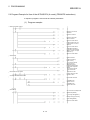
4.4 Offset/Gain Setting
When changing the I/O conversion characteristics, follow the procedure below.
START
Move the SELECT/SET switch to "SET". Confirm that
the "RUN" LED is lit* and release your hand.
Set all channels to any of "user range settings 1 to 3"
in the sequence program.
RUN
SELECT
Lit
SET
Short the TEST terminals (across 8-9) to enter the
test mode.
TEST
Change the lit offset/gain adjusting LEDs with the
SELECT/SET switch, and make sure that the LED of
the channel whose offset/gain will be set and the
"GAIN" LED are lit.
TEST
CH.1
2
3
OFFSET GAIN
4
Power ON
Lit
Lit
Start data link.
Add the voltage or current that will be the gain value.
Make sure that the "RUN" LED is off.
For voltage
V+
V
COM
A
Every time the SELECT/SET switch is moved to
"SELECT", the offset/gain adjusting LEDs lit change
as shown below.
CH.1
2
3
4
V+
COM
I+
For current
OFFSET GAIN
A
CH1 offset
value setting
CH1 gain
value setting
Move the SELECT/SET switch to "SET". Confirm that
the "RUN" LED is lit* and release your hand.
CH2 offset
value setting
CH2 gain
value setting
RUN
SELECT
Lit
SET
Change the lit offset/gain adjusting LEDs with the
SELECT/SET switch, and make sure that the LED
of the channel whose offset/gain will be set and the
"OFFSET" LED are lit.
CH.1
2
3
Adjust other channels?
OFFSET GAIN
4
Lit
NO
Lit
Open the TEST terminals (across 8-9).
The "RUN" LED is lit.
Add the voltage or current that will be the offset value.
TEST
TEST
For voltage
V+
V
COM
Power OFF
V+
COM
I+
For current
END
A
*: If the "RUN" LED is not lit, E2PROM may have failed. For details, refer to Section 6.1.
4-5
YES
A
4 SETUP AND PREPARATION BEFORE OPERATION
MELSEC-A
POINT
(1) Set the offset and gain values in the actual usage state.
(2) The offset and gain values are stored on E2PROM in the AJ65SBT-64AD and
are not cleared at power-off.
(3) Shorting the TEST terminals to enter the test mode and executing initial settings
will start A/D conversion on all channels. To judge the test mode, use the test
mode flag as an interlock.
(4) Make offset/gain setting within the range indicated in POINT of Section 3.3.1
and Section 3.3.2. If setting is made outside this range, the maximum
resolution/accuracy may not fall within the performance specifications range.
(5) When making offset/gain setting (in the test mode), set all channels to any of
"user range settings 1 to 3".
Setting any other range will result in an error and flicker the "RUN" LED at 0.1s
intervals.
Refer to Section 3.6.3 for input range setting.
(6) When the grounding indicated in Section 4.8.2 *5 is changed (not performed
perform, or performed to removed), repeat the offset/gain setting from the start.
4-6
4 SETUP AND PREPARATION BEFORE OPERATION
MELSEC-A
4.5 Station Number Setting
The station number setting of the AJ65SBT-64AD determines the buffer memory
addresses of the master module where the remote I/O signals and read/write data are
stored.
For details, refer to the user's manual of the master module used.
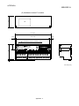
4.6 Facing Direction of the Module Installation
The AJ65SBT-64AD module may be installed in any of six directions.
(There are no restrictions on the facing directions.)
Also, a DIN rail may be used for installation.
Ceiling installation
DIN rail
Front installation
Flat installation
4-7
4 SETUP AND PREPARATION BEFORE OPERATION
MELSEC-A
4.7 Data Link Cable Wiring
This section explains the wiring of the CC-Link dedicated cable used for connection of
the AJ65SBT-64AD and master module.
4.7.1 Instructions for handling the CC-Link dedicated cables
Do not handle the CC-Link dedicated cables roughly as described below. Doing so can
damage the cables.
Compact with a sharp object.
Twist the cable excessively.
Pull the cable hard. (more than the permitted elasticity.)
Step on the cable.
Place an object on the top.
Scratch the cable's protective layer.
4.7.2 Connection of the CC-Link dedicated cables
Connect the CC-Link dedicated cable between the AJ65SBT-64AD and master
module as shown below.
Master module side
(Blue)
DA
(White)
Termination resistor
DB
(Yellow)
DG
SLD
FG
AJ65SBT-64AD
I/O module or like
DA
DB
DG
DA
DB
DG
CC-Link dedicated
cable
SLD
FG
4-8
CC-Link dedicated
cable
SLD
FG
Termination resistor
4 SETUP AND PREPARATION BEFORE OPERATION
MELSEC-A
4.8 Wiring
This section provides the instructions for wiring the AJ65SBT-64AD and its wiring with
external equipment.
4.8.1 Wiring precautions
To obtain maximum performance from the functions of AJ65SBT-64AD and improve
the system reliability, an external wiring with high durability against noise is required.
The precautions when performing external wiring are as follows:
(1) Use separate cables for the AC and AJ65SBT-64AD external input signals, in
order not to be affected by the AC side surge or conductivity.
(2) Do not bundle or place with load carrying wires other than the main circuit line,
high voltage line or PLC. Noises, surges, or conductivity may affect the system.
(3) Place a one-point grounding on the PLC side for the shielded line or shielded
cable. However, depending on the external noise conditions, it may be better have
a grounding externally.
4.8.2 Module connection example
For voltage input
Signal source 0 to ±10 V
*4
CH1
V+
I+
500k
250
500k
COM
SLD
*1 Shield
For current input
*2
Signal source 0 to ±20mA
CH4
*3
500k
V+
I+
COM
250
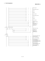
500k
SLD
*1 Shield
*5
AG
FG1
*1
*2
*3
*4
Use a two-core twisted shield line for the power cable.
Indicates the AJ65SBT-64AD input resistor.
For the current input, be sure to connect the (V+) and (I+) terminals.
When noise or ripple occurs with the external cable, connect a condenser with
about 0.1 to 0.47µF (25V or higher voltage-resistant product) between the terminal
V and COM.
*5 Always perform grounding for FG1. When there is a lot of noise, it may be better
ground AG as well.
If the grounding wiring (grounding yes/no) is changed after the offset and gain are
set, perform the setting of the offset/gain values again.
4-9
4 SETUP AND PREPARATION BEFORE OPERATION
MELSEC-A
POINT
• A/D conversion values are fluctuated by self-heating within approx. 30 minutes
after power is turned ON.
• In an unused channel, if terminals remain open, an erratic digital value may be output.
To prevent this, take any of the following measures.
1. Select Prohibit in the A/D conversion enable/prohibit setting for the unused channel.
Note that changing the setting from Enable to Prohibit will reduce the sampling cycle.
2. Short-circuit the input terminals (terminal V+ and COM) of the unused channel.
3. Connect the AG terminal to the GND terminal of the external device.
4.9 Maintenance and Inspection
There are no special inspection items for the AJ65SBT-64AD module, but follow the
inspections items describes in the PLC CPU User's Manual so that the system can
always be used in the best condition.
4 - 10
5 PROGRAMMING
MELSEC-A
5 PROGRAMMING
The programming procedure, basic read/write programs, and program examples for
the AJ65SBT-64AD are described.
When utilizing the program example introduced in this chapter for an actual system,
fully verify that there are no problems in controllability in the target system.
Refer to the user's manual of the master module used for the master module, to
Section 3.6 for the remote registers, and to the AnSHCPU/AnACPU/AnUCPU
Programming Manual (Dedicated Instructions) for details of the dedicated instructions.
5.1 Programming Procedure
Create a program which executes the AJ65SBT-64AD analog/digital conversion by
following the procedure below:
START
5
A/D conversion enable/prohibit specification
Input range setting
Perform moving average processing?
No
Initial settings*
Yes
Moving average processing count setting
Specify the channel for which moving average
processing will be performed.
Read digital output value
END
* When using the QCPU (Q mode), you can use the remote device station initialization
procedure registration function to make settings. When using the ACPU, QCPU (A
mode) or QnACPU, use the sequence program to make settings.
5-1
5 PROGRAMMING
MELSEC-A
5.2 Conditions of Program Example
The program examples in this chapter are created under the following conditions.
(1) System configuration
PLC CPU
Master station
(X0 to X1F/Y0 to Y1F)
I/O (Input 64 points)
(X20 to X5F)
I/O (Output 64 points)
(Y60 to Y9F)
AJ65SBT-64AD
(Station number 1)
(2) Relationships between PLC CPU, master module and AJ65SBT64AD
Master module
PLC CPU
Remote input (RX)
AJ65SBT-64AD
(Station number 1)
Remote input (RX)
Device X
X400 to X40F
Address
E0H
X410 to X41F
E1H
Device Y
Y400 to Y40F
160H
Y410 to Y41F
161H
Device D
D200
1E0H
RWw0
RWw0 A/D conversion
enable/prohibit specification
D201
1E1H
RWw1
RWw1 Input range setting
D202
1E2H
RWw2
RWw2 Moving average processing
count setting
D203
1E3H
RX00 to RX0F
RX00 to RX0F
RX10 to RX1F
RX10 to RX1F
Remote output (RY)
Remote output (RY)
RY00 to RY0F
RY00 to RY0F
RY10 to RY1F
RY10 to RY1F
Remote register (RWw)
Remote register (RWw)
RWw3
Remote register (RWr)
Device D*
RWw3 Reserved
Remote register (RWr)
D300
2E0H
RWr0
RWr0 CH.1 digital output value
D301
2E1H
RWr1
RWr1 CH.2 digital output value
D302
2E2H
RWr2
RWr2 CH.3 digital output value
D303
2E3H
RWr3
RWr3 CH.4 digital output value
* In the program example (refer to Section 5.5) that uses the RRPA instruction
(automatic refresh parameter setting) with the ACPU/QCPU (A mode), RWr0 to
RWr3 are assigned to D456 to D459.
POINT
Some CPU modules may not accept the devices used in the program example in
this chapter. For the setting ranges of the devices, refer to the user's manual of the
CPU module used.
For the A1SCPU, for example, devices X100, Y100 and later are unusable. Use
such devices as B and M.
5-2
5
5 PROGRAMMING
MELSEC-A
(3) Initial settings
Setting Item
Settings
A/D conversion enable/prohibit
specification (RWw0)
A/D conversion enabled channel: Channel 1, 2
Input range setting (RWw1)
Channel 1: 0 to 5V
Channel 2: User range setting 1
Moving average processing count setting
(RWw2)
Number of moving average processing times of
channel 2: 16times
CH.1 moving average processing
specifying flag (RY00)
Channel 1: Sampling processing
CH.2 moving average processing
specifying (RY01)
Channel 2: Moving average processing
5-3
5 PROGRAMMING
MELSEC-A
5.3 Program Example for Use of the QCPU (Q mode)
The program examples in this section are created under the following conditions.
GX Developer is used to set the network and automatic refresh parameters.
Using the remote device station initialization procedure registration function facilitates
initial settings.
(1) Parameter setting
(a) Network parameter setting
(b) Automatic refresh parameter setting
5-4
5 PROGRAMMING
MELSEC-A
(2) Initial setting by remote device station initialization procedure
registration
(a) Setting the target station number
Set the station number to which initial setting will be made.
Set the target station number to "1".
(b) Setting the procedure registration
When the initial data processing request flag (RX18) turns on and the
remote device station initialization procedure registration (SB0D) is set, the
following data are registered to the AJ65SBT-64AD.
Procedure Execution Condition
Execution
A/D conversion enable/prohibit specification: channels 1, 2: enable
(RWw0: 0003H)
Input range setting : channel 1: 0 to 5V
: channel 2: user range setting 1
(RWw1: 51H)
Initial data processing request flag (RX18) turns on
Moving average processing count setting: channel 2: 16 times
(RWw5: 10H)
CH.1 moving average processing specifying flag: sampling processing
(RY00:OFF)
CH.2 moving average processing specifying flag: moving average processing
(RY01:ON)
Initial data processing completion flag (RY18) is turned on.
Initial data setting request flag (RY19) is turned on.
Initial data processing request flag (RX18) turns off
Initial data processing completion flag (RY18) is turned off.
Initial data setting completion flag (RX19) turns on
Initial data setting request flag (RY19) is turned off.
(c) Setting results
The setting results are shown below.
5-5
5 PROGRAMMING
MELSEC-A
(3) Program example
Checking of AJ65SBT-64AD status
Reads data link status
AJ65SBT-64AD
data link normal
AJ65SBT-64AD
data link abnormal
Initialization procedure registration
1
1)
Turns off initialization procedure
registration
Turns on initialization procedure
registration
2
2)
Changing of initial settings
Initial setting change
A/D conversion enable/prohibit
specification(RWw0)
Input range setting(RWw1)
Moving average processing count
setting(RWw2)
CH.1 moving average processing
specifying flag(RY00)
CH.2 moving average processing
specifying flag(RY01)
Turns on initial data setting
request flag(RY19)
Turns off initial data setting
request flag(RY19)
Read of digital values
Reads CH.1 digital output value
(RWr0)
Reads CH.2 digital output value
(RWr1)
Processing at error occurrence
Turns on Y91 at CH.1 range error
occurrence
Turns on Y92 at CH.2 range error
occurrence
Turns on Y93 at CH.3 range error
occurrence
Turns on Y94 at CH.4 range error
occurrence
Turns on Y95 at E2PROM write
error occurrence
Error reset
Turns on error reset request flag
(RY1A)
Turns off error reset request flag
(RY1A)
5-6
5 PROGRAMMING
MELSEC-A
*1 When making remote device station initialization procedure registration to multiple
stations, correct the program within the dotted line 1) as shown below.
RX(m+1)B and RX(n+1)B are remote READY.
RX(m+1)8 and RX(n+1)8 are initial data processing request flags.
The device numbers change depending on the station number. Insert the remote
READY and initial data processing request flags for all the stations, to which the
remote device station initialization procedure registration has been made, into the
program.
SB5F
RX(m+1)B RX(n+1)B
RX(m+1)8
RX(n+1)8
*2 The program enclosed by the dotted line 2) is necessary only when the initial
settings are changed.
5-7
5 PROGRAMMING
MELSEC-A
5.4 Program Example for Use of the QnACPU
GX Developer is used to set the network and automatic refresh parameters.
(1) Parameter setting
(a) Network parameter setting
(b) Automatic refresh parameter setting
5-8
5 PROGRAMMING
MELSEC-A
(2) Program example
Checking of AJ65SBT-64AD status
Reads data link status
AJ65SBT-64AD
data link normal
AJ65SBT-64AD
data link abnormal
Initial settings
A/D conversion enable/prohibit
specification(RWw0)
Input range setting(RWw1)
Moving average processing
count setting(RWw2)
CH.1 moving average processing
specifying flag(RY00)
CH.2 moving average processing
specifying flag(RY01)
Turns on initial data processing
completion flag(RY18)
Turns on initial data setting
request flag(RY19)
Changing of initial settings
Initial setting change
A/D conversion enable/prohibit
specification(RWw0)
Input range setting(RWw1)
Moving average processing
count setting(RWw2)
CH.1 moving average processing
specifying flag(RY00)
CH.2 moving average processing
specifying flag(RY01)
Turns on initial data setting
request flag(RY19)
Processing at initial settings
Turns off initial data processing
completion flag(RY18)
Turns off initial data setting
request flag(RY19)
Read of digital values
Reads CH.1 digital output value
(RWr0)
Reads CH.2 digital output value
(RWr1)
* The program enclosed by the dotted line is necessary only when the initial settings
are changed.
5-9
5 PROGRAMMING
MELSEC-A
Processing at error occurrence
Turns on Y91 at CH.1 range
error occurrence
Turns on Y92 at CH.2 range
error occurrence
Turns on Y93 at CH.3 range
error occurrence
Turns on Y94 at CH.4 range
error occurrence
Turns on Y95 at E2PROM write
error occurrence
Error reset
Turns on error reset request flag
(RY1A)
Turns off error reset request flag
(RY1A)
5 - 10
5 PROGRAMMING
MELSEC-A
5.5 Program Example for Use of the ACPU/QCPU (A mode) (dedicated instructions)
A sequence program is used to set the network and automatic refresh parameters.
(1) Program example
Setting of network parameters using RLPA dedicated instruction
Synchronization mode invalid
Number of connected
modules:1
AJ65SBT-64AD station
information (remote device
station, 1 station occupied,
station No. 1)
Dedicated instruction (RLPA)
Starting I/O number of master
module
Parameter storage starting
device
Device which turns on 1 scan
at completion
Reads parameter status at
abnormal completion.
Setting of automatic refresh parameters using RRPA dedicated instruction
Sets RX starting number.
Sets "X".
Sets X400.
Sets 32 points.
Sets RY starting number.
Sets "Y".
Sets Y400.
Sets 32 points.
Sets RW starting number.
Sets "D".
Sets D200.
5 - 11
5 PROGRAMMING
MELSEC-A
Sets 261 points.
Sets SB starting number.
Sets "B".
Sets B0.
Sets 512 points.
Sets SW starting number.
Sets "W".
Sets W0.
Sets 256 points.
Dedicated instruction
(RRPA)
Starting I/O number of
master module
Parameter storage
starting device
Checking of AJ65SBT-64AD status
Reads data link status.
AJ65SBT-64AD
data link normal
AJ65SBT-64AD
data link abnormal
Initial settings
A/D conversion enable/prohibit
specification(RWw0)
Input range setting(RWw1)
Moving average processing
count setting(RWw2)
CH.1 moving average processing
specifying flag(RY00)
CH.2 moving average processing
specifying flag(RY01)
Turns on initial data processing
completion flag(RY18)
Turns on initial data setting
request flag(RY19)
5 - 12
5 PROGRAMMING
MELSEC-A
Changing of initial settings
Initial setting change
A/D conversion enable/
prohibit specification
(RWw0)
Input range setting(RWw1)
Moving average processing
count setting(RWw2)
CH.1 moving average
processing specifying flag
(RY00)
CH.2 moving average
processing specifying flag
(RY01)
Turns on initial data setting
request flag(RY19)
Processing at initial settings
Turns off initial data
processing completion flag
(RY18)
Turns off initial data setting
request flag(RY19)
Read of digital values
Reads CH.1 digital output
value(RWr0)
Reads CH.2 digital output
value(RWr1)
Processing at error occurrence
Turns on Y91 at CH.1 range
error occurrence
Turns on Y92 at CH.2 range
error occurrence
Turns on Y93 at CH.3 range
error occurrence
Turns on Y94 at CH.4 range
error occurrence
Turns on Y95 at E2PROM
write error occurrence
Error reset
Turns on error reset request
flag(RY1A)
Turns off error reset request
flag(RY1A)
* The program enclosed by the dotted line is necessary only when the initial settings
are changed.
5 - 13
5 PROGRAMMING
MELSEC-A
5.6 Program Example for Use of the ACPU/QCPU (A mode) (FROM/TO instructions)
A sequence program is used to set the network parameters.
(1) Program example
Network parameter settings
Number of connected
modules: 1
Number of retries: 3
Number of automatic
return modules: 1
Writes to master station
Data link status when the
master station PLC CPU:
continue
Writes to master station
AJ65SBT-64AD station
information (remote device
station, 1 station occupied,
station No. 1)
Writes to master station
Start data link
Refresh directive
Data link started by
buffer memory
Turns off start request
signal at normal
completion of start.
Reads parameter status
at abnormal completion
of start.
Turns off start request
signal at abnormal
completion of start.
Read of remote input signals
RX00 to RX1F are read
to X400 to X41F
Checking of AJ65SBT-64AD status
Reads data link status.
AJ65SBT-64AD
data link normal
AJ65SBT-64AD
data link abnormal
Initial settings
A/D conversion enable/prohibit
specification(RWw0)
Input range setting(RWw1)
Moving average processing
count setting(RWw2)
Writes to master station
5 - 14
5 PROGRAMMING
MELSEC-A
CH.1 moving average
processing specifying flag
(RY00)
CH.2 moving average
processing specifying flag
(RY01)
Turns on initial data
processing completion flag
(RY18)
Turns on initial data setting
request flag(RY19)
Changing of initial settings
Initial setting change
A/D conversion enable/
prohibit specification
(RWw0)
Input range setting(RWw1)
Moving average processing
count setting(RWw2)
Writes to master station
CH.1 moving average
processing specifying flag
(RY00)
CH.2 moving average
processing specifying flag
(RY01)
Turns on initial data setting
request flag(RY19)
Processing at initial settings
Turns off initial data
processing completion flag
(RY18)
Turns off initial data setting
request flag(RY19)
Read of digital values
Reads CH.1 digital output
value(RWr0)
Reads CH.2 digital output
value(RWr1)
Processing at error occurrence
Turns on Y91 at CH.1 range
error occurrence
Turns on Y92 at CH.2 range
error occurrence
Turns on Y93 at CH.3 range
error occurrence
Turns on Y94 at CH.4 range
error occurrence
Turns on Y95 at E2PROM
write error occurrence
Error reset
Turns on error reset request
flag(RY1A)
Turns off error reset request
flag(RY1A)
Write of remote output signals
Y400 to Y41F are written
into RY00 to RYIF
* The program enclosed by the dotted line is necessary only when the initial settings
are changed.
5 - 15
6 TROUBLESHOOTING
MELSEC-A
6 TROUBLESHOOTING
The details of the errors which may occur when using the AJ65SBT-64AD and
troubleshooting are described.
6.1 Using the Remote Input Signals to Check Errors
In the AJ65SBT-64AD, occurrence of a write error turns on any of the following remote
input signals.
Device No.
Signal Name
RXn4
CH.1 range error flag
RXn5
CH.2 range error flag
RXn6
CH.3 range error flag
RXn7
CH.4 range error flag
RXnC
E2PROM write error flag
Description
Turns on when the value set for input range setting is outside the setting range.
Turns on if all channels are not set to any of "user range settings 1 to 3" at offset/gain
setting (in the test mode).
Turns on if value write failed due to excess of the E2PROM write count over its limit at the
time of offset/gain setting.
If this flag has turned on, this module itself has failed (hardware fault) and therefore this flag
cannot be reset (turned off) by the error reset request flag.
Turns on when CH.
RX(n+1)A
Error status flag
range error flag (RXn4 to RXn7) or E2PROM write error flag (RXnC)
has turned on.
This flag can be reset (turned off) by turning on the error reset request flag. However, for
the E2PROM write error which cannot be reset, this flag cannot be reset, either.
(1) For the input range error (RXn4 to RXn7), the "RUN" LED flickers at intervals of
0.1s and A/D conversion is not performed on all channels.
(2) For the E2PROM write error (RXnC), power on the AJ65SBT-64AD again.
If the E2PROM write error (RXnC) turns on after power is switched on again, it
indicates a hardware fault. Contact your nearest Mitsubishi representative.
6-1
6
6 TROUBLESHOOTING
MELSEC-A
6.2 Using the LED Indications to Check Errors
This section explains how to check errors using the LED indications of the AJ65SBT64AD.
Refer to the PLC CPU and master module user's manual for issues regarding the PLC
CPU and master module.
(1) When the AJ65SBT-64AD "PW" LED is off
Check item
Corrective action
Is 24VDC power on?
Check the external power supply.
Is the voltage of the 24VDC power supply within
the specified value?
Set the voltage value to within the range 20.4 to
26.4V.
(2) When the AJ65SBT-64AD "RUN" LED is flashing
Check item
Corrective action
Is the LED flickering at 0.1s intervals in the
normal mode?
6
1. Using the remote input signals (RXn4 to RXn7),
check the channel at which the input range setting
error has occurred.
2. Make correction to the sequence program or
GPPW setting.
Is the LED flickering at 0.1s intervals in the test
mode?
Set all channels to any of "user range settings 1 to 3"
in input range setting.
Is the LED flickering at 0.5s intervals in the test
mode?
Change the offset/gain adjustment to within the
available setting range.
(3) When the AJ65SBT-64AD "RUN" LED is off
Check item
Corrective action
Has the watchdog timer error occurred?
Has the TEST terminals (across 8-9) been
shorted to enter the test mode?
Using the link special registers (SW0084 to SW0087)
of the master module, check the watchdog timer error
and power on the AJ65SBT-64AD again.
If the "RUN" LED is not lit after power is switched on
again, the possible cause is a hardware fault. Contact
your nearest Mitsubishi representative.
After making offset/gain adjustment, open the TEST
terminals (across 8-9).
(4) When the AJ65SBT-64AD "L RUN" LED is off
Communications are broken.
For details, refer to troubleshooting in the user's manual of the master module
used.
6-2
6 TROUBLESHOOTING
MELSEC-A
(5) When the AJ65SBT-64AD "L ERR." LED flickers at fixed intervals
Check item
Corrective action
Has the station number or transmission speed
setting switch position been changed during
normal operation?
After correcting the setting switch setting, switch
power on again.
Is the station number or transmission speed
setting switch faulty?
If the "L ERR." LED has begun flickering though
switch setting change was not made during operation,
the possible cause is a hardware fault. Contact your
nearest Mitsubishi representative.
(6) When the AJ65SBT-64AD "L ERR." LED flickers at unfixed intervals
Check item
Corrective action
Have you forgotten fitting the terminal resistor?
Is the module or CC-Link dedicated cable
affected by noise?
Check whether the terminal resistor is fitted. If it is not
connected, connect it and switch power on again.
Earth both ends of the shield wire of the CC-Link
dedicated cable to the protective earth conductor via
SLD and FG of the corresponding module.
Earth the FG terminal of the module without fail.
When carrying out wiring in piping, earth the pipe
without fail.
(7) When the AJ65SBT-64AD "L ERR." LED is on
Check item
Corrective action
Are the station number and transmission speed
correct?
6-3
Set the correct station number and transmission
speed.
6 TROUBLESHOOTING
MELSEC-A
6.3 When the digital output value cannot be read
Check item
Corrective action
Is the "PW" LED off?
Take action as described in Section 6.2 (1).
Is the "RUN" LED flashing or off?
Take action as described in Section 6.2 (2), (3).
Is the "L RUN" LED off?
Take action as described in Section 6.2 (4).
Is the "L ERR." LED on?
Take action as described in Section 6.2 (7).
Check the error details according to the master
module user's manual.
Is the PLC CPU "RUN" LED flashing or off?
Check the error details according to the PLC CPU
user's manual.
Is the master module "RUN" LED off?
Check the error details according to the master
module user's manual.
Is the master module [RD] [SD] LED on?
Check the error details according to the master
module user's manual.
Is the analog input signal line disconnected, cut
off, or any errors?
Check the error area by checking the signal line
visually or by conductive check.
Remove the AJ65SBT-64AD analog input cable.
Apply the test voltage (stable power supply or
battery) to this module's terminal, and measure the
digital output value.
If he AJ65SBT-64AD module digital output value is
normal, the effects are being received by noise from
an external wiring. So check the wiring and
grounding method.
Lift the AJ65SBT-64AD from the system, and
remove the grounding circuit. (install to the DIN rail.)
6-4
6 TROUBLESHOOTING
MELSEC-A
6.4 Troubleshooting for the Case where the "ERR." LED of the Master Station Flickers
The "ERR."LED on the
master station is flashing
Do the parameter
setting and the installed system
configuration match
properly?
N
Revise the parameter settings
or installed system configuration
Y
Are the master
station link special registers
SW0080 to SW0083 (other station
date link status)
turned on?
N
Master station malfunction
Y
Are the master
station link special registers
SW0098 to SW009B (station
number overlap status)
turned on?
N
Y
Check the module for which
SW0098 to SW009B are on
Are the
station number setting
switches set
properly?
Y
Check on master station side
Check the module for which
SW0080 to SW0083 are on
N
Is the power on?
Set the station number setting
swiches properly
Check on slave station side
N
Turn on the power
Y
Turn on the power again
Is the "POWER" LED lit?
N
Corresponding module
malfunction
Y
Is the supplied
power within the specified
range
Y
N
Set the supplied voltage to
within the specified range
Corresponding module
malfunction
1
2
6-5
3
6 TROUBLESHOOTING
1
MELSEC-A
2
3
N
Is the "L RUN" LED lit?
Y
Are the
station number
setting switches properly
(not overlapping with
other stations)?
N
Set the station number
setting switches properly
Y
Turn on the power again
Is the transmission speed
setting correct?
Y
N
Set the correct transmission speed
Turn on the power again
N
Is the communication
cable wired properlly ?
*1
Y
Wire the communication
cable properly
Corresponding module malfunction
( Transmission speed setting switch )
Are the
station number
setting switches properly
(not overlapping with
other stations)?
Y
N
Set the station number
setting switches properly
Turn on the power again
Corresponding module malfunction
( station number setting switch )
End
*1 Check for a short, reversed connection, wire breakage, terminal resistor, FG connection,
overall distance and station-to-station distance.
6-6
APPENDIX
MELSEC-A
APPENDIX
Appendix 1 Comparison between This Product and Conventional Product
(1) Comparison in performance between this product and conventional
product
The following table gives performance comparison between the AJ65SBT-64AD
and conventional product (AJ65BT-64AD).
Performance Comparison between AJ65SBT-64AD and Conventional Product
Specifications
Item
Analog input
AJ65SBT-64AD
AJ65BT-64AD
Voltage
-10 to +10VDC (input resistance: 1M )
-10 to +10VDC (input resistance: 1M )
Current
0 to 20mADC (input resistance: 250 )
-20 to +20mADC (input resistance: 250 )
-4096 to +4095
-4000 to +4000
Digital output
Digital
Output
Input Range
Max.
Resolution
-10 to +10V
User range
setting 1
(-10 to +10V)
Voltage
I/O characteristics
Maximum resolution
-10 to +10V
-4000 to
+4000
2.5mV
Voltage
0 to 10V
0 to 5V
0 to 4000 or
-2000 to
+2000
1 to 5V
0 to 5V
1.25mV
0 to 4000
0 to 20mA
Max.
Resolution
5mV
2.5mV
1.25mV
1.0mV
-20 to +20mA
1 to 5V
User range
setting 2
(0 to 5V)
Digital
Output
Input Range
Current
1.0mV
0 to 20mA
0 to 20mA
20µA
0 to 4000 or
-2000 to
+2000
10µA
4 to 20mA
5µA
4µA
5µA
4 to 20mA
Current
Input range changing
User range
setting 3
(0 to 20mA)
0 to 4000
4µA
Per channel
All channels in batch
Offset/gain setting
Accuracy
Yes
Ambient
temperature
0 to 55°C
±0.4%
(accuracy relative to maximum value of digital output value)
±1.0%
(accuracy relative to maximum value of digital output value)
Ambient
temperature
25±5°C
±0.2% (accuracy relative to maximum value of digital output
value)
————
Max. conversion speed
Absolute max. input
1ms/channel
Voltage ±15V, current ±30mA
Number of analog input
points
Number of occupied I/O
points
Voltage ±15V, current ±30mA
4 channels/module
1 station occupied
(RX/RY: 32 points each, RWr/RWw: 4 points each)
2 stations occupied
(RX/RY: 32 points each, RWr/RWw: 8 points each)
7-point, 2-piece terminal block (transmission, power supply)
Direct-coupled,
18-point terminal block (analog input section) (M3 screw)
27-point terminal block (M3.5 screw)
Applicable wire size
0.3 to 0.75mm2
0.75 to 2.00mm2
Applicable crimping
terminal
RAV1.25-3
RAV1.25-3.5, RAV2-3.5
0.090A
0.12A
Connected terminal block
24VDC internal current
consumption
Weight
Outline dimensions
0.20kg
0.35 kg
118mm(W) × 50mm(H) × 40mm(D)
151.9mm(W) × 65mm(H) × 63mm(D)
Appendix - 1
APP
APPENDIX
MELSEC-A
(2) Precautions for replacing the conventional product (AJ65BT-64AD)
with the AJ65SBT-64AD
In the existing system using the conventional product (AJ65BT-64AD), the
following instructions must be noted when changing the AJ65BT-64AD for the
AJ65SBT-64AD.
(a) Since the AJ65SBT-64AD occupies one station (the AJ65BT-64AD occupies
two stations), the station information setting in the network parameters must
be changed.
(b) As the remote I/O signals and remote register settings are different between
the two models, the program of the conventional model cannot be utilized.
(c) Because of the differences in shape and layout between the terminal blocks,
you cannot use the terminal block of the conventional module as it is.
(d) The offset/gain setting method differs. For details, refer to Section 4.4.
(e) The ways to set the station number and transmission speed setting switches
are different. For details, refer to Section 4.3.
APP
Appendix - 2
APPENDIX
MELSEC-A
Appendix 2 External Dimensions
The external dimensions of the AJ65SBT-64AD is shown below.
The appearance of the AJ65SBT-64AD varies depending on the hardware version.
For checking method of the hardware version, refer to Section 2.3.
40 (1.57)
(1) Hardware version F or later
118 (4.65)
109
[4.5]
(0.18)
+1
0
(4.29)
[4.5]
(0.18)
OFFSETGAIN
SELECT
AJ65SBT-64AD
DA DG +24V
DB SLD
24G
(FG)
CH1
STATION NO.
B RATE
40 20 10 8 4 2 1 4 2 1
ON
SET
CH2
CH3
CH4
TEST
COM SLD COM AG
V+
I+
V+
I+
TEST COM SLD
COM
V+
I+
V+
I+
(FG1)
7.5
(0.30)
RUN L RUN L ERR. CH12 3 4
DIN rail center
7.9
(0.31)
4
(0.16)
50 (1.97)
PW
05
t1
ou
Ab
16.5
(0.65)
2-4.5 5.1 installation hole (M4 installation screw)
Unit: mm (inch)
Appendix - 3
APPENDIX
MELSEC-A
40
(1.57)
(2) Hardware version E or earlier
NP
118 (4.65)
[4.5]
109 (4.29)
[4.5]
(0.18)
(0.18)
16.5
(0.65)
2-4.5 5.1 installation hole (M4 installation screw)
PW
RUN L RUN L ERR. CH1 2
4
OFFSET GAIN
AJ65SBT-64AD
SELECT
STATION NO.
B RATE
40 20 10 8 4 2 1 4 2 1
ON
SET
CH1
CH2
CH3
CH4
TEST V+
V+
I+
COM SLD COM AG
I+
(FG1)
TEST COM SLD COM V+
V+
I+
I+
4
(0.16)
50
(1.97)
MITSUBISHI
DA DG +24V 24G
DB SLD
(FG)
3
Unit: mm (inch)
Appendix - 4
INDEX
Ind
[A]
A/D conversion completion flag .................... 3-11
A/D conversion enable/prohibit specification
....................................................................... 3-14
Absolute maximum input................................. 3-2
Accuracy.................................................... 3-2,3-6
Analog input..................................................... 3-2
Analog input points.......................................... 3-2
Applicable master modules............................. 2-2
Input range setting .........................................3-15
Input range setting error ..................................6-1
[M]
Maintenance and inspection..........................4-10
Maximum resolution.................................. 3-2,3-6
Module connection example............................4-9
Moving average processing ............................3-9
Moving average processing count setting ....3-16
Moving average processing specifying flag ..3-12
[C]
CC-Link dedicated cable................................. 4-8
CC-Link dedicated instruction......................... 2-2
Conversion speed ........................................... 3-7
Current consumption....................................... 3-2
Current input characteristics ........................... 3-5
[N]
Name of each part ...........................................4-3
Number of occupied stations...........................3-2
[O]
Offset value ......................................................3-3
Offset/gain adjusting LED................................4-3
Offset/Gain Setting...........................................4-5
Operation status display LED..........................4-3
[D]
Data link cable wiring ...................................... 4-8
Digital output.................................................... 3-2
Digital output value........................................ 3-16
DIN rail.................................................3-2,4-2,4-4
[P]
Performance comparison between AJ65SBT64AD and conventional product ................. App-1
Performance specification ...............................3-2
Pre-Operation procedure.................................4-1
Precautions for replacing the conventional
product (AJ65BT-64AD) with the AJ65SBT-64AD
..................................................................... App-2
Precautions when handling .............................4-1
Program example for use of the QCPU (Q mode)
..........................................................................5-4
Program example for use of the QnACPU .....5-8
Program example for use of the ACPU/QCPU
(A mode) (dedicated instructions) .................5-11
Program example for use of the ACPU/QCPU
(A mode) (FROM/TO instructions) ...............5-14
Programming procedure..................................5-1
[E]
E2PROM write error flag ............................... 3-11
Error reset request flag ................................. 3-12
Error status flag ............................................. 3-12
External dimensions....................................App-3
External power supply..................................... 3-2
[F]
Facing direction of the module installation ..... 4-7
Function list ..................................................... 3-8
[G]
Gain value ....................................................... 3-3
General specification....................................... 3-1
[I]
I/O Conversion Characteristics ....................... 3-3
Initial data processing completion flag ......... 3-12
Initial data processing request flag ............... 3-11
Initial data setting completion flag................. 3-11
Initial data setting request flag ...................... 3-12
Input range changing function ........................ 3-8
[R]
Range error flag ...................................... 3-11,6-1
Remote I/O signal list.....................................3-10
Remote READY.............................................3-12
Remote register allocation.............................3-13
Resolution ........................................................3-6
Index - 1
[S]
Ind
Sampling processing....................................... 3-9
SELECT/SET switch ....................................... 4-3
Station number setting switch......................... 4-4
[T]
Terminal block ........................................... 3-2,4-4
Terminal number ............................................. 4-3
Test mode flag............................................... 3-11
Tightening torque range.................................. 4-2
Troubleshooting............................................... 6-1
Troubleshooting for the case where the
"ERR."LED of the master station flickers ....... 6-5
[U]
User range setting ..................................... 3-4,3-5
[V]
Voltage input characteristics ........................... 3-4
[W]
Weight.............................................................. 3-2
Wiring............................................................... 4-9
Index - 2
MEMO
Index - 3
WARRANTY
Please confirm the following product warranty details before using this product.
1. Gratis Warranty Term and Gratis Warranty Range
If any faults or defects (hereinafter "Failure") found to be the responsibility of Mitsubishi occurs during use of the product
within the gratis warranty term, the product shall be repaired at no cost via the sales representative or Mitsubishi Service
Company.
However, if repairs are required onsite at domestic or overseas location, expenses to send an engineer will be solely at
the customer’s discretion. Mitsubishi shall not be held responsible for any re-commissioning, maintenance, or testing onsite that involves replacement of the failed module.
[Gratis Warranty Term]
The gratis warranty term of the product shall be for one year after the date of purchase or delivery to a designated
place.
Note that after manufacture and shipment from Mitsubishi, the maximum distribution period shall be six (6) months, and
the longest gratis warranty term after manufacturing shall be eighteen (18) months. The gratis warranty term of repair
parts shall not exceed the gratis warranty term before repairs.
[Gratis Warranty Range]
(1) The range shall be limited to normal use within the usage state, usage methods and usage environment, etc.,
which follow the conditions and precautions, etc., given in the instruction manual, user's manual and caution labels
on the product.
(2) Even within the gratis warranty term, repairs shall be charged for in the following cases.
1. Failure occurring from inappropriate storage or handling, carelessness or negligence by the user. Failure caused
by the user's hardware or software design.
2. Failure caused by unapproved modifications, etc., to the product by the user.
3. When the Mitsubishi product is assembled into a user's device, Failure that could have been avoided if functions
or structures, judged as necessary in the legal safety measures the user's device is subject to or as necessary
by industry standards, had been provided.
4. Failure that could have been avoided if consumable parts (battery, backlight, fuse, etc.) designated in the
instruction manual had been correctly serviced or replaced.
5. Failure caused by external irresistible forces such as fires or abnormal voltages, and Failure caused by force
majeure such as earthquakes, lightning, wind and water damage.
6. Failure caused by reasons unpredictable by scientific technology standards at time of shipment from Mitsubishi.
7. Any other failure found not to be the responsibility of Mitsubishi or that admitted not to be so by the user.
2. Onerous repair term after discontinuation of production
(1) Mitsubishi shall accept onerous product repairs for seven (7) years after production of the product is discontinued.
Discontinuation of production shall be notified with Mitsubishi Technical Bulletins, etc.
(2) Product supply (including repair parts) is not available after production is discontinued.
3. Overseas service
Overseas, repairs shall be accepted by Mitsubishi's local overseas FA Center. Note that the repair conditions at each FA
Center may differ.
4. Exclusion of loss in opportunity and secondary loss from warranty liability
Regardless of the gratis warranty term, Mitsubishi shall not be liable for compensation of damages caused by any cause
found not to be the responsibility of Mitsubishi, loss in opportunity, lost profits incurred to the user by Failures of Mitsubishi
products, special damages and secondary damages whether foreseeable or not , compensation for accidents, and
compensation for damages to products other than Mitsubishi products, replacement by the user, maintenance of on-site
equipment, start-up test run and other tasks.
5. Changes in product specifications
The specifications given in the catalogs, manuals or technical documents are subject to change without prior notice.
6. Product application
(1) In using the Mitsubishi MELSEC programmable controller, the usage conditions shall be that the application will not
lead to a major accident even if any problem or fault should occur in the programmable controller device, and that
backup and fail-safe functions are systematically provided outside of the device for any problem or fault.
(2) The Mitsubishi programmable controller has been designed and manufactured for applications in general industries,
etc. Thus, applications in which the public could be affected such as in nuclear power plants and other power plants
operated by respective power companies, and applications in which a special quality assurance system is required,
such as for Railway companies or Public service purposes shall be excluded from the programmable controller
applications.
In addition, applications in which human life or property that could be greatly affected, such as in aircraft, medical
applications, incineration and fuel devices, manned transportation, equipment for recreation and amusement, and
safety devices, shall also be excluded from the programmable controller range of applications.
However, in certain cases, some applications may be possible, providing the user consults their local Mitsubishi
representative outlining the special requirements of the project, and providing that all parties concerned agree to the
special circumstances, solely at the users discretion.
Analog-Digital Converter Module Type AJ65SBT-64AD
,
User s Manual
MODEL
AJ65S-64AD-U-S-E
MODEL
CODE
13JR18
SH(NA)-080106-E(0701)MEE
HEAD OFFICE : TOKYO BUILDING, 2-7-3 MARUNOUCHI, CHIYODA-KU, TOKYO 100-8310, JAPAN
NAGOYA WORKS : 1-14 , YADA-MINAMI 5-CHOME , HIGASHI-KU, NAGOYA , JAPAN
When exported from Japan, this manual does not require application to the
Ministry of Economy, Trade and Industry for service transaction permission.
Specifications subject to change without notice.