1
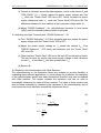
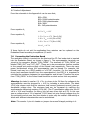
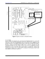
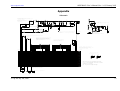
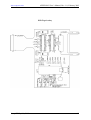
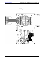
www.cap-xx.com
APPEB1004 User’s Manual, Rev. 1.0, March 2003
cap-XX
Compact Flash™ Extender
and Supercapacitor
Evaluation Board
Part No. APPEB1004
User’s Manual
Revision 1.0
March, 2003
Evaluation Board
Features
•
•
•
•
•
CF Extender
Supercapacitor (two form factors)
Adjustable current limit circuit with Supercapacitor charge enable
3.3V and 5V input LEDs
Supercapacitor voltage comparator with adjustable
threshold, adjustable hysteresis and Power Good LED
• Card Detect switches to simulate card removal and insertion
• Sub-circuits can be disconnected to reduce the load
• Test points, jumpers and I/O connectors
Typical Supercapacitor
Applications
•
•
•
•
•
•
•
Compact Flash
PC card
PDA
Smartphone
GPRS
Handheld Equipment
Load Leveling
© cap-XX Pty Ltd, 2003
1
www.cap-xx.com
APPEB1004 User’s Manual, Rev. 1.0, March 2003
Contents
1.0
Introduction
3
2.0
Input Voltage
3
2.1 Charge Time
3
3.0
Current Limit
4
4.0
Enable
4
5.0
Power Good
4
6.0
Adjusting the Circuit
5
6.1 Adjusting the Current Limit with “Current Limit” - R2
6.2 Adjusting Hysterisis Width with “PGOOD Feedback” - R23
6.3 Adjusting the High Threshold with “PGOOD Reference” - R15
6.4 Replacing the Potentiometers with Fixed Resistors
6.5 Limits of Adjustment
6
6
7
7
8
Connecting the Evaluation Board
8
7.1 VCC Modes
7.2 Current Measurement
7.3 Card Detect
7.4 Voltage Select
9
10
11
11
Disconnecting Circuits for Reduced Load
11
7.0
8.0
Appendix
Schematic
PCB Top Overlay
PCB Top Layer
PCB 2nd Layer
PCB 3rd Layer
PCB Bottom Layer
© cap-XX Pty Ltd, 2003
12
12
13
14
15
16
17
2
www.cap-xx.com
APPEB1004 User’s Manual, Rev. 1.0, March 2003
1.0 Introduction
This User’s Manual is for the cap-XX Compact Flash™ (CF) Extender and
Supercapacitor Evaluation Board (Part No. APPEB1004). This board was designed for
the evaluation of a supercapacitor in a CF Card. The application of supercapacitors is
limited only by the user’s imagination. Typical examples are CF, PC Card, PDA,
Smartphone, GPRS and other handheld equipment.
The Evaluation Board is a CF Extender with a supercapacitor, a current limit circuit
and other features.
An excellent source for information on Supercapacitors and free downloads are
available on the cap-XX website at www.cap-xx.com.
In the following description of operation it may be helpful to refer to the Evaluation
Board Schematic in the Appendix.
2.0 Input Voltage
The supercapacitors for the Evaluation Board are rated at 4.5V and therefore it is not
recommended that the input voltage (VCC) be greater than 4.5V. If VCC is 5V then the
Equivalent Series Resistance (ESR) rise rate of the supercapacitor is increased and
the lifetime will be reduced. A red LED is included to indicate that VCC is too high and
it starts to glow when VCC is approximately 4.2V. The red LED is labeled on the
Evaluation Board as “5 Volts”. If VCC is 5V then the voltage can be dropped to < 4.5V
by removing a jumper which introduces a series diode in the voltage supply lines on
the Evaluation Board (see section 7.0). A yellow LED is included to indicate when VCC
is 3.3V or greater. It is labeled on the Evaluation Board as “3.3 Volts”.
If VCC is disconnected (or if the Evaluation Board is removed from the host) and
there is still charge on the supercapacitor then current will flow through the body
diode of M1 and through the yellow LED (also through the red LED if the
supercapacitor is greater than ~ 4.2V). The intensity of the yellow LED then gives an
indication of the voltage remaining on the supercapacitor. If, however, the series
diode has been included to reduce the 5V rail to 4.5V then the LEDs will not be ON
when VCC is disconnected.
2.1 Charge Time
A fully discharged supercapacitor will be charged to VCC after a certain time (tc). This
time will depend on the current limit (IL), VCC and the capacitance (C). The equation
is
tc =
© cap-XX Pty Ltd, 2003
CVCC
IL
(1)
3
www.cap-xx.com
APPEB1004 User’s Manual, Rev. 1.0, March 2003
3.0 Current Limit
Circuits that employ large capacitors generally need a current limiting circuit to
alleviate the current in-rush problem. The CF specification states that the peak
current is 500mA from either the 3.3V or 5V rail. The tolerance on the 3.3V rail is ±
5% and the tolerance on the 5V rail is ± 10%. Therefore the peak power from the
3.3V rail is 1.65W ± 5% and the 5V rail is 2.5W ± 10%.
The Evaluation Board has an adjustable current limit circuit. The current limit can be
adjusted from 0A to ~ 4.5A by using the potentiometer R2. It is labeled on the
Evaluation Board as “Current Limit”. Turning the potentiometer clockwise will
increase the current limit.
The MOSFET (M1) and Sense Resistor (R1) can withstand up to 4.5A whilst the
supercapacitor is being charged. They cannot however withstand the 4.5A into a
short circuit indefinitely. There is no short circuit protection. The MOSFET (M1) has a
maximum continuous power dissipation of 2.5W. Therefore any continuous load
resistance (RL) has a minimum value as given by equation 2.
VCC I L − 2.5
I 2L
RL = 0
RL ≥
[VCC I L > 2.5]
(2)
[VCC I L ≤ 2.5]
RL also has a minimum power rating according to equation 3.
PR L > I 2L R L
PR L
2
VCC
>
RL
[input current = IL]
(3)
[input current < IL]
4.0 Enable
The current limit circuit has an enable feature. Enable is an active low signal and the
two pin jumper is labeled on the Evaluation Board as “J_ENABLE”. It is an input
signal to the Evaluation Board and it can be jumpered to ground, to be permanently
enabled, or it can be externally driven by an open collector or drain. When
“J_ENABLE” is externally driven it allows the supercapacitor to be charged only when
the User’s Card is ready. Pin 2 of “J_ENABLE” is the control input and Pin 1 is
permanently connected to ground.
5.0 Power Good
The Power Good circuit (PGOOD) is included to indicate when the supercapacitor is
charged to the appropriate level. The voltage on the supercapacitor is compared to a
reference using a comparator with adjustable thresholds and hysteresis. The
thresholds need to be adjustable on an Evaluation Board because different
applications will require different load voltages. The hysteresis also needs to be
adjustable because a step in load current will cause a step voltage on the
supercapacitor because of the supercapacitor’s Equivalent Series Resistance (ESR).
© cap-XX Pty Ltd, 2003
4
www.cap-xx.com
APPEB1004 User’s Manual, Rev. 1.0, March 2003
Since this step voltage (part of the ripple) is a normal occurrence, it would not be
desirable for this to indicate that the supercapacitor is undercharged.
Power
Good
LED On
LED Off
VTL
VW
Vcc
VTH
Figure 1 Power Good Hysteresis
As in Figure 1, the high threshold (VTH) is the voltage at which the supercapacitor’s
unloaded voltage becomes acceptable. The hysteresis (VW) is the voltage that when
subtracted from the high threshold gives the low threshold (VTL). It indicates that the
supercapacitor is undercharged. VTH is set by the factory at 3.2V and VW is set at
0.3V, therefore VTL is 2.9V.
PGOOD has a header labeled on the Evaluation Board as “H_PGOOD”. It is an active
high output signal that can be used to signal an external circuit that the
supercapacitor is fully charged. A green LED is also included to indicate this
condition. It is labeled on the Evaluation Board as “Power Good”.
6.0 Adjusting the Circuit
Equipment needed: Adjustable power supply, multi-meter and various power
resistors
Warning: Be careful not to exceed the supercapacitor rated voltage (4.5V) or the
maximum continuous power rating for M1 (2.5W)
(a) Ensure the following jumpers are fitted; “J_RED&YLW”, “J_GREEN”,
“J_PGOOD”, “J_ENABLE”, “J_VCC13_IN” (pins 3 and 4), “J_VCC38_IN”
(pins 3 and 4) and “J_5V”. Remove jumpers on “J_VCC13_OUT” and
“J_VCC38_OUT”. Pin 1 is marked with “∇”.
(b) Turn “Current Limit” - R2 fully anti-clockwise (no current). Set the power
supply voltage to say 3.3VDC. Ensure that the power supply can supply
the desired current. Connect its negative lead to J_GND1 or J_GND2.
Connect the positive lead to pin 1 of “J_VCC13_IN”.
(c) Set the power supply output voltage to a value < 4.5V.
6.1 Adjusting the Current Limit with “Current Limit” - R2
Warning: the maximum average power rating for M1 is 2.5W (see section 3.0)
(a) Connect a load resistor to “CON_CAPXX” (RL) that draws just over the
desired current limit from the CF host (typically 500mA). Note the power
© cap-XX Pty Ltd, 2003
5
www.cap-xx.com
APPEB1004 User’s Manual, Rev. 1.0, March 2003
rating of the resistor is according to equation 3 and RL has a minimum
value according to equation 2. For example, if the supply voltage is 3.3V
and the desired current limit is 500mA then an RL < 6.6Ω would draw
more than 500mA. RL can then be chosen to be the next standard value <
6.6Ω, ie 5.7Ω. From equation 3, the power rating of the 5.7Ω resistor
would have to be > 1.43W. In this particular example, and according to
equation 2, RL can also be a short circuit as this would not overload M1.
(b) Place an ammeter in series with the power supply. Turn on the power
supply and adjust “Current Limit” - R2 slowly clockwise until the desired
current limit is reached.
Warning: Do not increase the current limit above that used in equations 2
and 3 for any longer than a few seconds otherwise M1 or RL may be
destroyed.
(c) Remove RL, turn off the power supply.
6.2 Adjusting Hysteresis Width with “PGOOD Feedback” - R23
NOTE: VW is adjusted before VTH because the VTH adjustment is affected by VW.
Therefore if adjustments are made in this section then section 6.3 should be
checked.
(a) If the CF card is to be driven from the 5V rail, then remove the jumper
across “J_5V”, otherwise, if the PC Card is to be driven from the 3.3V rail,
then fit the jumper across “J_5V”.
(b) Connect a load power resistor (RL) of around 10Ω-47Ω from “VCC_OUT” to
“GND_OUT” on “CON_CAPXX”. This ensures that the supercapacitor
voltage will change in reasonable time when the power supply voltage is
changed. Note the power rating of RL has to be a minimum value
according to equation 3.
(c) Turn the “PGOOD Reference” - R15 to around mid position (about 11 turns
from either limit).
(d) Decide the high threshold voltage VTH , the low threshold voltage VTL and
the hysteresis voltage width VW (Vw = VTH - VTL). VTL has to be greater
than the minimum voltage required by the Pulsed Load. VW has to be
greater than the expected voltage droop due to the ESR and capacitor
discharge etc.
(e) The LED labeled “3.3 Volts” should now be ON and the LED labeled
“Power Good” should also be ON. If “Power Good” is not ON, then turn
“PGOOD Reference” - R15 anticlockwise slowly until the “Power Good” LED
is ON.
© cap-XX Pty Ltd, 2003
6
www.cap-xx.com
APPEB1004 User’s Manual, Rev. 1.0, March 2003
(f) Connect a voltmeter across the supercapacitor, which is also across RL and
“CON_CAPXX” ( VR L ). Slowly reduce the power supply voltage and note
VR L when the “Power Good” LED turns OFF. Slowly increase the power
supply voltage and note VR L when the “Power Good” LED turns ON. The
difference between the two readings is the hysteresis voltage width Vw.
(g) Adjust “PGOOD Feedback” - R23 (anti-clockwise increases Vw) and repeat
(e)&(f) until the desired hysteresis width is achieved.
6.3 Adjusting the High Threshold with “PGOOD Reference” - R15
(a) Turn “PGOOD Reference” - R15 fully clockwise and then reduce the power
supply voltage until the “Power Good” LED is OFF.
(b) Adjust the power supply voltage so VR L equals the desired VTH. Turn
“PGOOD Reference” - R15 slowly anti-clockwise until the “Power Good”
LED turns ON.
(c) Check that the “Power Good” LED turns ON and OFF at the desired levels.
This can be done by varying the power supply voltage in both directions
so that VR L is less than VTL and then greater than VTH.
(d) Remove RL.
6.4 Replacing the Potentiometers with Fixed Resistors
The potentiometers on the Evaluation Board are included to provide flexibility in
evaluating many different applications. In a final design for production the resistance
of the potentiometers would have been decided and therefore they can be replaced
with fixed resistors. This section includes the equations that can be used to
theoretically determine the value of these resistors. The value of these resistors can
also be found practically by measuring the resistance of the potentiometers out of
circuit once the circuit has been successfully adjusted as above.
R 22 + R 23 =
55k
VW
(4)
R15 + R16 =
4k 7VTH
5 + VW − VTH
(5)
R2 =
© cap-XX Pty Ltd, 2003
22k
56
−1
IL
(6)
7
www.cap-xx.com
APPEB1004 User’s Manual, Rev. 1.0, March 2003
6.5 Limits of Adjustment
From the schematic in the Appendix it can be seen that;
R22=47kΩ
R23=500kΩ potentiometer
R15=50kΩ potentiometer
R16=3k9Ω
R2= 2kΩ potentiometer
From equation 4;
From equation 5;
From equation 6;
0.1V ≤ VW ≤ 1.2V
2.3V ≤ VTH ≤ 4.7 V (VW=0.1V)
2.4V ≤ VTH ≤ 4.9V (VW=0.3V)
2.8V ≤ VTH ≤ 5.7 V (VW=1.2V)
0A ≤ I L ≤ 4.7 A
If these limits do not suit the application then resistors can be replaced on the
Evaluation Board according to equations 4,5 and 6.
7.0 Connecting the Evaluation Board
The evaluation board is inserted into the Host and the CF Card under test is inserted
into the Evaluation Board, as shown in figure 2. The supercapacitor terminals are
joined to the connector labeled “CON_CAPXX”. The terminals of “CON_CAPXX” are
labeled “GND_OUT” and “VCC_OUT”. These are to be connected as close as possible
to the ground and positive supply of the Pulsed Load respectively. There are many
power architectures where the supercapacitor may be placed. For example, the
Pulsed Load may be a GPRS module or a DC/DC converter. For the least voltage
droop (and maximum benefit from the supercapacitor’s low ESR) it is important to
minimise the resistance between the supercapacitor and its load. Therefore the wires
from “CON_CAPXX” to the Pulsed Load should be as short and as thick as practical.
Warning: As stated in section 2.0, if VCC is chosen to be 5V then the voltage at the
supercapacitor must be dropped to < 4.5V by including a series diode. The diode
(D10) was chosen such that the minimum load current (quiescent current) gives an
acceptable voltage drop. The minimum load can be increased by reducing the
supercapacitor balancing resistors (R5 & R6). The CF specification states that the 5V
rail is ± 10% and therefore (in theory) the rail may be as high as 5.5V. In this rare
case a voltage drop of 1V is required. If D10 does not give enough voltage drop for
the minimum current case then two diodes in series may be needed. Alternatively a
diode with different characteristics can be substituted.
Note: The number 1 pin of a header or jumper has a small triangle pointing to it.
© cap-XX Pty Ltd, 2003
8
www.cap-xx.com
APPEB1004 User’s Manual, Rev. 1.0, March 2003
CF Card Under Test
H
O
S
T
Pulsed loads
Other
Circuitry
(eg GPRS Module,
DC/DC converter)
V+
GND
Figure 2 Typical connection of Evaluation Board
7.1 VCC Modes
Figure 2 shows the typical way for connecting the Evaluation Board. VCC on the CF
Card Under Test is generally supplied by one of two modes. Mode 1, being the most
common, is when VCC is supplied directly from the host (via “J_CF_HEADER” pins 13
and 38). These VCC rails supply all the circuitry on the CF Card Under Test (“Other
Circuitry”) except for the “Pulsed loads (V+)”, which is supplied by the
supercapacitor with the external wires. In this mode VCC is available to the “Other
Circuitry” as soon as the CF Card Under Test is powered up, whereas the
supercapacitor supply to the “Pulsed loads” is delayed by the charge up time of the
supercapacitor according to equation 1.
© cap-XX Pty Ltd, 2003
9
www.cap-xx.com
APPEB1004 User’s Manual, Rev. 1.0, March 2003
Connections common to both Mode 1 and 2 are;
(a) Connect external wires (thick and short) from “CON_CAPXX” to the
“Pulsed loads” on the CF Card Under Test.
(b) Place jumpers on pins 3 and 4 of “J_VCC13_IN” and “J_VCC38_IN”.
Remember to use the series diode (remove “J_5V”) if using the 5V rail.
(c) Place jumpers
“J_ENABLE”,.
on
“J_RED&YLW”,
“J_GREEN”,
“J_PGOOD”
and
(d) Remove jumpers on “J_VS1”, “J_VS2”.
Mode 1 is accomplished by the following;
(a) Connect jumpers on “J_VCC13” and “J_VCC38”.
(b) Remove jumpers across pins 1-2 of both “JVCC_13_OUT” and
“JVCC_38_OUT”. Make sure that VCC on the CF card under test is not
connected to the Pulsed Load V+. Otherwise VCC will be short circuited by
the supercapacitor when it is discharged and the current limit circuit is not
in this path.
Mode 2 is when the supercapacitor supplies both the VCC for the PC Card Under Test
(“Other Circuitry”) as well as the “Pulsed loads”. In this mode all supplies are
delayed according to equation 1. Any voltage ripple on the supercapacitor due to
large currents will appear on the VCC rail.
Mode 2 is accomplished by the following;
(a) Remove the jumpers on “J_VCC13” and “J_VCC38”.
(b) Either ensure that VCC on the CF card under test is connected to the
Pulsed Load V+ and supply the load via thick wires as per Figure 2 or
place jumpers across pins 1-2 of both “JVCC_13_OUT” and
“JVCC_38_OUT”.
There are many other modes available. The Evaluation board is designed for
flexibility by allowing each section to be isolated or connected to external circuits.
NOTE: Care must be taken, in which ever mode is chosen, so that the charge up
time of the supercapacitor does not affect the operation of any reset or power rail
monitoring circuitry etc. As described in section 4.0 and 5.0, the “J_ENABLE” and
“H_PGOOD” signals may need to be interfaced with the CF Card Under Test for
proper control.
7.2 Current Measurement
Currents can be measured with a current probe or a voltage across a sense resistor.
A jumper can be replaced by an external wire loop which the current probe can
clamp on. If a current probe is not available then a sense resistor can be used in
© cap-XX Pty Ltd, 2003
10
www.cap-xx.com
APPEB1004 User’s Manual, Rev. 1.0, March 2003
place of the jumpers. The voltage dropped across the resistor divided by the value of
the resistor equals the current.
7.3 Card Detect
The correct insertion of a CF Card is detected when both pins 25 and 26 are
grounded. These pins are typically grounded on the CF Card Under Test. However,
the ground signal can also be replicated by jumpering –CD1 and –CD2 to ground on
“J_Test1” and “J_Test2”. The removal and insertion of the card can be simulated by
depressing and releasing either of the two micro-switches “SW_CD1” or “SW_CD2”.
7.4 Voltage Select
The CF Card Under Test chooses the VCC voltage rail using pin 33 (-VS1). If -VS1 is
grounded then a VCC of 3.3V is requested, if it is left floating then 5V is requested.
This signal can be replicated with “J_VS1”. Placing a jumper on “J_VS1” forces the
signal to ground and therefore requests 3.3V. “J_VS2” is undefined and should be
left floating.
8.0 Disconnecting Circuits for Reduced Load
The minimum voltage on some loads may be critical. Any current that the Evaluation
Board uses contributes to the droop on the input voltage. If the droop becomes
excessive then some of the functions on the Evaluation Board can be disconnected
to save current and therefore increase the input voltage. The red and yellow LEDS
can be disconnected by removing the jumper “J_RED&YLW”. The green LED can be
disconnected by removing the jumper “J_GREEN”. The entire PGOOD circuit can be
disconnected by removing the jumper “J_PGOOD”.
© cap-XX Pty Ltd, 2003
11
www.cap-xx.com
APPEB1003 User’s Manual, Rev. 1.0, February 2003
Appendix
Schematic
The supercapacitor and current limit circuit can be isolated
by removing the jumpers on J_VCC13_IN, J_VCC38_IN,
J_VCC13_OUT and J_VCC38_OUT.
1
Remove jumper J_5V if the rail is 5 Volts.
This gives a diode drop to keep the
supercap under 4.5V.
VCC_IN
1
M1
SUD45P03-10
22m
TP7
JUMPER1
J_5V
R3
10k
C2
D1
TP8
1
1
2
C1
47n
R2
2k
LM4041DIM3-1.2
D10
22k
R7
22
TP9
R10
3
M2
-
FDV302P
R5
39k
1
CX1
3
R8
39k
470
3
H_CAPXX
R9
1
+
J_VCC13_IN
CON4
Vcapxx
TS1852
8
2
1
10k
R4
10k
47n
VCC_IN
R6
RS1A
1 2 3 4
CON4
J_VCC38_IN
R13
680
R1
VCC_IN
2
+
The intensity of the Yellow LED gives an indication of the voltage on the
supercap when VCC_IN is disconnected, but only when J_5V is connected.
D8
R11
BAT54J
470
D2
VCC_IN
TP5
1
50k
R15
Vcapxx
FDV301N
C4
47n
TEST POINT
1
TP6
VCC_IN
TS1852
4
6
J_Enable can have its jumper removed and can be driven
by an external open collector if desired.
2
J_ENABLE
-
5
+
JUMPER1
Power Good Circuit.
If H_PGOOD is high then the supercap rail is good.
TP4
R16
3k9
R17
22k
C3
100n
Place cap close to pin 8.
J_RED&Y LW
Y ellow_LED
Schottkys
1
capxx
M3
U1A
Vr
1
4
1 2 3 4
R14
4k7
2
JUMPER1
1
-
D5
ZRC250
2
2
R
8
R20
22k
H_PGOOD
R19
7
1
U1B
VCC_IN
3
TP3
1
R12
BAT54J
220
D3
D4
R23
1
1
1
R21
TP2
1
BZX84C3V3
Q1
BCX20
4k7
TP1
2
R22 + R23 = 22k*2.5/Vw
JUMPER1
3
Red_LED
D6
Green_LED
JUMPER1
2
500k
R22
2
D7
ZRC250
47k
D9
R18
470
2
680
1
1
2
Vw = width of hysteresis
Vh = high threshold
Vr = reference
2
JUMPER1
CON2
J_GREEN
JUMPER1
Vr = Vh/(Vw/2.5+2)
J_PGOOD
CON_CAPXX
CON_CAPXX is to connect low resistance leads from Vcapxx to the
CF card so there is a low resistance path from the supercap
to the load.
1
Linking all POWER GOOD grounds and then jumpering to common ground
allows the POWER GOOD circuit to be disconnected.
SW_CD1
Normally Closed
These spring loaded switches simulate card removal and insertion.
D2FL
Normally Closed
SW_CD2
If VCC_IN is 5V then both the Red and Yellow LEDs will be on.
If VCC_IN is 3.3V then only the Yellow LED will be on.
These LEDs will also be powered by the supercapacitor
through the body diode of the current limiting Mosfet when
VCC_IN is disconnected by the host.
The LEDs can be disconnected so as to not load the circuit.
D2FL
-CD1 and -CD2 can simply be grounded with
jumpers across pins 25&26 on J_Test2 and
pins 25&26 on J_Test1 respectively.
J_VCC13_OUT
CON3
1 2 3
J_Test1
1
3
5
7
9
11
13
15
17
19
21
23
25
J_Test2
2
4
6
8
10
12
14
16
18
20
22
24
26
JUMPER13
1
3
5
7
9
11
13
15
17
19
21
23
25
2
4
6
8
10
12
14
16
18
20
22
24
26
1 2 3
J_VCC38_OUT
CON3
J_VCC13_OUT, J_VCC38_OUT, J_VCC13 and J_VCC38 can
have their jumpers removed and an external supply can be
connected to J_VCC13_OUT (pin 2 or 3) and
J_VCC38_OUT (pin 2 or 3) if desired.
JUMPER13
J_CF_SOCKET
J_CF_HEADER
1
2
3
4
5
6
7
8
9
10
11
12
13
14
15
16
17
18
19
20
21
22
23
24
25
26
27
28
29
30
31
32
33
34
35
36
37
38
39
40
41
42
43
44
45
46
47
48
49
50
GND
D03
D04
D05
D06
D07
-CE1
A10
-OE
A09
A08
A07
VCC13
A06
A05
A04
A03
A02
A01
A00
D00
D01
D02
-IOIS16
-CD2
-CD1
D11
D12
D13
D14
D15
-CE2
-VS1
-IORD
-IOWR
-WE
IREQ
VCC38
-CSEL
-VS2
RESET
-WAIT
-INPACK
-REG
-SPKR
-STSCHG
D08
D09
D10
GND
HEADER 50
Placing jumpers on J_VCC13 and J_VCC38 passes VCC
straight through to the CF card. In this case remove jumpers
from J_VCC13_OUT and J_VCC38_OUT or the
supercapacitor will short circuit the VCC rail.
J_VCC38
JUMPER1
1
2
J_VS1
1
2
JUMPER1
1
J_GND 1&2 are test points to safely
put the CRO ground aligator clip.
J_GND1
1
J_GND2
2
JUMPER1
1
2
JUMPER1
The board can be configured such that
it is a pure extender card with no extra
loading or circuitry
ie, all pins straight through.
CONN SOCKET 50
J_VS2
2
JUMPER1
1
2
3
4
5
6
7
8
9
10
11
12
13
14
15
16
17
18
19
20
21
22
23
24
25
26
27
28
29
30
31
32
33
34
35
36
37
38
39
40
41
42
43
44
45
46
47
48
49
50
1
2
Jumpering J_VS1 to ground ensures 3.3V.
JUMPER1
J_VCC13
© cap-XX Pty Ltd, 2003
12
www.cap-xx.com
APPEB1003 User’s Manual, Rev. 1.0, February 2003
PCB Top Overlay
© cap-XX Pty Ltd, 2003
13
www.cap-xx.com
APPEB1003 User’s Manual, Rev. 1.0, February 2003
PCB Top Layer
© cap-XX Pty Ltd, 2003
14
www.cap-xx.com
APPEB1003 User’s Manual, Rev. 1.0, February 2003
PCB 2nd Layer
© cap-XX Pty Ltd, 2003
15
www.cap-xx.com
APPEB1003 User’s Manual, Rev. 1.0, February 2003
PCB 3rd Layer
© cap-XX Pty Ltd, 2003
16
www.cap-xx.com
APPEB1003 User’s Manual, Rev. 1.0, February 2003
PCB Bottom Layer
© cap-XX Pty Ltd, 2003
17