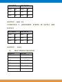
1
Contents
CHAPTER 1: INTRODUCTION ................................................... 4
1.1 INTRODUCTION ................................................................. 4
1.2 PS – 8086 BOARD OVERVIEW ...................................... 5
1.3 PS – 8086 SPECIFICATIONS ......................................... 6
CHAPTER – 2: SYSTEM DESCRIPTION ..................................... 7
2.1 HARDWARE ................................................................... 7
1) 20 PIN EXPANSION CONNECTORS: ............................. 9
The 20 Pin FRC connector is used to interconnect with the
Interface cards like ADC, DAC, SWITCH/LED, RELAY
buzzer Interfaces etc. Pin details are given below ................. 9
2) 50 PIN EXPANSION CONNECTOR: ............................. 10
The 50 Pin FRC connector is used to interconnect with the
Interface cards like 8255, 8279, 8253/8251, 8259, 8257 and
the pin details are given below ............................................ 10
2.4 KEYBOARD DETAILS .................................................. 14
CHAPTER – 3 COMMANDS AND KEYS ................................... 14
3.1 Reset............................................................................. 14
3.2 H (HELP MENU).......................................................... 14
CHAPTER – 4 OPERATING INSTRUCTIONS ......................... 15
4.1 POWER ON ................................................................... 15
4.2 Instruction ................................................................... 16
1) PROGRAM ENTRY USING ASSEMBLER: .................... 16
ENTERING MNEMONICS ................................................... 16
ENTERING ‘G‘EXECUTING COMMAND ............................. 19
4.3 ENTERING RESULT COMMAND: ................................. 19
4.4 DISASSEMBLER ........................................................... 20
4.5 M (Modify External Memory): .................................... 21
4.6 R (Register Display) .................................................... 21
4.7 T (Transfer Command) ............................................... 22
4.8 N (Local Mode) ........................................................... 23
4.9 B (baud rate) ............................................................... 24
4.10 S (Serial Mode Key) .................................................. 24
1) Initially connect the 9V adaptor to J10 connector ............. 25
CHAPTER 6: EXAMPLE PROGRAMS ...................................... 30
6.1 Addition Of Two Bytes Of Data ....................................... 30
6.3 MULTIPLICATION OF TWO BYTE DATA .................. 34
6.4 DIVISION (2 BYTE/ 1 BYTE) ..................................... 36
6.5 BLOCK MOVE FROM ONE LOCATION TO ANOTHER38
6.6 SEARCHING A BYTE ................................................... 41
6.7 GRAY CODE CONVERSION (Look Up Table) ............. 43
6.8 SUM OF N CONSECUTIVE NUMBERS ........................ 45
6.9 ASCII TO HEX CODE CONVERSION ........................... 46
6.10 BCD TO HEXA DECIMAL CONVERSION .................. 48
6.11 HEXA DECIMAL TO ASCII CODE.............................. 50
6.12 MATRIX ADDITION ................................................... 51
6.13 SEPERATING ODD AND EVEN................................. 54
6.14 FIBONACCI SERIES .................................................. 56
6.15 FACTORIAL OF A NUMBER ..................................... 58
6.16 FIND THE LARGEST NUMBER IN AN ARRAY .......... 60
6.17 AVERAGE OF AN ARRAYError!
Bookmark
not
defined.
6.18 GENERATE SQUARE WAVE ..................................... 64
6.19 DESCENDING ORDER .............................................. 65
6.20 ASCENDING ORDER ................................................. 68
CHAPTER 1: INTRODUCTION
1.1 INTRODUCTION
The
PS-8086 board
which
demonstrates
the
capabilities of the 40-pin 8086 (various families) Sample
programs are provided to demonstrate the unique
features of the supported devices.
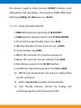
The PS-8086 Kit comes with the following:
1) PS-8086 Board
2) Sample devices (INTEL 8086/NEC 8086)
3) Cross cable (RS232)
4) CD-ROM, which contains:
a) Sample programs
b) PS-8086 Board User manual
5) Keyboard (101 keys)
Note: If you are missing any part of the kit, please
contact our support executive
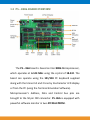
1.2 PS – 8086 BOARD OVERVIEW
The PS – 86A board is based on Intel 8086 Microprocessor,
which operates at 6.144 MHz using the crystal of 18.432. The
board can operate using the 101/104 PC keyboard supplied
along with the trainer kit and 2 Line by 16-character LCD display
or from the PC (using the Terminal Emulation Software).
Microprocessor’s Address, Data and Control bus pins are
brought to the 50 pin FRC connector. PS -86A is equipped with
powerful software monitor in two-27C256 EPROM.
The monitor supports Video terminal RS232C interface, local
101keyboard and LCD display. The board has 64KB CMOS static
RAM (type 62256). PS -86A works on +9V DC.
1.3 PS – 8086 SPECIFICATIONS
1. 8086 Microprocessor operating at 18.432 MHz
2. 16KB powerful software monitor two 27C256 EPROM
3. Three 16-bit programmable timers from 8253
4. 48 programmable I/O lines from two nos. of 8255
5. Serial interface using 8251
6. 50 pin FRC connector for system bus expansion
7. 20 pin FRC connector for user interface from 8255
8. 9 pin D type connectors for RS 232 interface
9. Six different selectable baud rates from 150 to 9600
10. 101 PC type keyboard for entering user address/data
and for commands
11. Built in line-by-line assemble and disassemble
12. User friendly software monitor for loading and
executing programs with break point facility
CHAPTER – 2: SYSTEM DESCRIPTION
2.1 HARDWARE
PROCESSOR CLOCK FREQUNCY:
8086 operates at 18.432 MHz clock.
MEMORY:
Monitor EPROM: 0000 –FFFF (SEGMENT)
System RAM:
0000 –FFFF (SEGMENT)
1000 – 3FFF (Reserved For Monitor program)
User RAM Area:
1100 – 3FFF
ALLOCATION OF EPROM:
START
ADDRESS
0000
END ADDRESS SOCKET
NO
FFFF
U9
U8
IC
USED
27256
27256
TOTAL
CAPACITY
32 K BYTE
32 K BYTE
IC
USED
62256
62256
TOTAL
CAPACITY
32 K BYTE
32 K BYTE
ALLOCATION OF RAM:
START
ADDRESS
0000
END ADDRESS SOCKET
NO
FFFF
U10
U11
PARALLEL INTERFACE:
8255
- Programmable peripheral interface.
SYSTEM MAPPING: I/O mapped I/O.
The following are the I/O addresses for 8255(GPIO I):
SOCKET.NO FUNCTION
U22
CONTL REG
PORT A
PORT B
PORT C
ADDRESS
FF26
FF20
FF22
FF24
CONNECTOR.NO
J8
GPIO I
J9(GPIO
I&GPIOII)
The following are the I/O addresses for 8255(GPIO II):
SOCKET.NO FUNCTION
U16
CONTL REG
PORT A
PORT B
PORT C
ADDRESS
CONNECTOR.NO
FF36
FF30
FF32
FF34
J6
GPIO II
J9(GPI0 I&GPIOII)
TIMER INTERFACE:
8253 - Programmable Interval Timer:
SYSTEM MAPPING: I/O mapped I/O.
CHANNEL 2:
Input clock : 3 MHz
Output clock: Depends on selection of baud
rate.
Used for
: Baud rate generation for 8521
USART.
I/O ADDRESS:
SOCKET.NO FUNCTION
U12
CONTL REG
CHENNAL 0
CHENNAL 1
CHANNEL 2
ADDRESS
CONNECTOR.NO
FF06
FF00
FF02
FF04
J2
2.2 CONNECTOR DETAILS
1) 20 PIN EXPANSION CONNECTORS:
The 20 Pin FRC connector is used to interconnect with the
Interface cards like ADC, DAC, SWITCH/LED, RELAY buzzer
Interfaces etc. Pin details are given below
J6
PA00
PA02
PA04
PA06
PB00
PB02
PB04
PB06
5V
1
3
5
7
9
11
13
15
17
19
J8
2
4
6
8
10
12
14
16
18
20
PA01
PA03
PA05
PA07
PB01
PB03
PB05
PB07
GND
GND
J9
1
3
5
7
9
11
13
15
17
19
PA0
PA2
PA4
PA6
PB0
PB2
PB4
PB6
5V
20-PIN FRC
2
4
6
8
10
12
14
16
18
20
PA1
PA3
PA5
PA7
PB1
PB3
PB5
PB7
GND
GND
PC0
PC2
PC4
PC6
PC00
PC02
PC04
PC06
5V
20-PIN FRC
1
3
5
7
9
11
13
15
17
19
2
4
6
8
10
12
14
16
18
20
PC1
PC3
PC5
PC7
PC01
PC03
PC05
PC07
GND
GND
20-PIN FRC
2) 50 PIN EXPANSION CONNECTOR:
The 50 Pin FRC connector is used to interconnect with the
Interface cards like 8255, 8279, 8253/8251, 8259, 8257 and the
pin details are given below
J7
GND
D0
D2
D4
D6
A0
A2
A4
A6
A8
A10
A12
A14
PCLK
RESET
INTR
NC
HLDA
WR
ALE
NC
NC
CS9
RXD
5V
1
3
5
7
9
11
13
15
17
19
21
23
25
27
29
31
33
35
37
39
41
43
45
47
49
HEADER 25X2
2
4
6
8
10
12
14
16
18
20
22
24
26
28
30
32
34
36
38
40
42
44
46
48
50
D1
D3
D5
D7
A1
A3
A5
A7
A9
A11
A13
A15
BHE
INTA
NMI
HOLD
RD
MIO
NC
NC
CS8
CS10
TXD
GND
5V
3) KEYBOARD CONNECTOR:
2 – PC7 K/B data
4 – GND
1 – PC6 K/B CLK
3 – NC
5 – VCC
4) 9PIN ‘D’ TYPE (FEMALE):
NC
NC
P1
1
6
2
7
3
8
4
9
5
RXD
CTS
TXD
NC
NC
NC
GND
8251 - Universal Synchronous / Asynchronous Receiver /
Transmitter.
RS232 Bridge Converter
BAUD CLOCK:
Baud clock for 8251 is programmable, provided by
Channel 2 of 8253
INPUT CLOCK FOR 8251:
3.072 MHz
DRIVERS USED:
MAX 232 is used for transmitting receiving of characters.
8251 Uart I/O Address:
SOCKET.NO FUNCTION
ADDRESS
8251
CONTL
FF10
U15
REG
FF12
8251 DATA
5) LCD Interface:
LCD
JP1
1
1
2
3
4
5
6
7
8
9
10
11
12
13
14
15
16
2X16 LCD
LCD
RS
RW
E
D0
D1
D2
D3
D4
D5
D6
D7
2
10K
R1
3
LCD
CONNECTOR.NO
D2(SKT)
Device used: 16 × 2 / 20 × 4 LCD module
System Mapping: I/O mapped I/O.
SOCKET.NO FUNCTION
ADDRESS
LCD COMMAND
FF40
---LCD DATA
FF42
CONNECTOR.NO
-----
6) RESET:
This key is located in the main 8086 board. On depressing
this key the program starts executing from the beginning or
reset address 0000. On power on reset it. Display PS - 86 in local
LCD display.
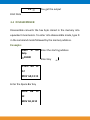
2.3 POWER SUPPLY DETAILS:
PS trainer kit will work at 0 – 5v (1 amp) from the PS power
supply. Provision is made in PS power supply to bring out on
the front panel DC regulated voltage output for interfacing with
add-on cards.
+5V
1 amp
Supply Turned OFF
POWER SWITCH
Supply Turned ON
2.4 KEYBOARD DETAILS
101 PC type keyboard is interfaced to Microcontroller
through its port pin. Communication between keyboard and
Microcontroller takes place using 2 wires – one for serial clock
and serial data (P1.6 and P1.7).
CHAPTER – 3 COMMANDS AND KEYS
3.1 Reset
This key is located in the main PS-86A board .On
depressing this key the programs. Starts executing from the
beginning or reset address 0000. On power on reset it. Displays
PS- 86A in local LCD display
PS -86
!!!!
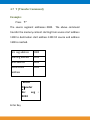
3.2 H (HELP MENU)
This key is used go PS- 86A help menu and it will display
the following commands.
KEY
A <BEG>
B
D <BEG>
E <BEG><END>
G <BEG>
H
I <INSERT>
L <OFFSET>
M <ADDR>
N
Q
R <REG>
S
T
<START><END><DS>
U <BEG><END>
X
?
FUNCTIONS
ASSEMBLE
BAUD RATE
DISASSEMBLE
EXAMINE
EXECUTE
HELP COMMANDS
INTERNAL RAM
DOWN LODE
MODIFY
NORMAL MODE
QUIT
REGISTER DISPLAY
SERIAL TRANSFER
BLOCK TRENSFER
UP LODE
DELETE
BLACK
MEMORY
INSTRUCTIONS
CHAPTER – 4 OPERATING INSTRUCTIONS
4.1 POWER ON
Connect the PS – 8051 board to the power having the
following specifications.
+9V DC 1 Amp
Switch on the power supply after ensuring the correct voltages.
Following message will appear on the LCD display.
PS -- 86
!!!!
On power on or after reset the display shows PS – 86 as a sign
on message. The prompt character – is displayed in the next line
informing the user, that the board is ready to accept the
commands.
4.2 Instruction
1)
PROGRAM ENTRY USING ASSEMBLER:
ENTERING MNEMONICS
Example:
Press H for Enter the starting Address
help
A1100
Enter Key
User program starts from address 1100 and displays the
following and waits for the user data to be typed in the second
line
Example:
0000 : 1100:
MOV AX,1212
Enter the mnemonics
0000 : 1103:
Enter the mnemonics
Enter Key
MOV BX,1212
Enter Key
Program end.
Exit Command: Double Enter you get the main menu
86
▁
PS
2) PROGRAM ENTRY USING OPCODE:
Modify Memory
Press H for Enter the starting Address
help
▁M1100
Enter Key
0000:1100:
18 ▁
0000:1100:
Enter the opcode
18 B8▁
Enter the Space Bar Key
0000:1101:
Enter the opcode
34 12▁
Enter the Space Bar Key
Program end. Exit Command:
Double Enter you get the Main Menu
ENTERING ‘G‘EXECUTING COMMAND
PS
Enter starting address
86
▁G1100
Enter key
After executing display
PS
Executing display
86
▁G1100
To EXIT Execution Mode PRESS ’RESET ‘Switch
4.3 ENTERING RESULT COMMAND:
Press H for Enter the Memory Location
help
▁M
<address>
0000:1200:
Enter Key
24 ▁
You get the output
8-bit Data
4.4 DISASSEMBLER
Disassemble converts the hex byte stored in the memory into
equivalent mnemonics. To enter into disassemble mode, type D
in the command mode followed by the memory address.
Example:
Press H
help
▁D1100
for Enter the starting address
Enter Key
1100: B8 12
12
MOV AX,1212
Enter the Space Bar Key
1103: BB 12
12
MOV AX,1212
Enter the space bar key
4.5 M (Modify External Memory):
Using this command the user can display/modify any external
memory address.
Modify External memory
Press H for Enter the starting Address
help
▁M1100
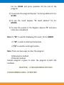
4.6 R (Register Display)
Example:
Press H for Enter the starting Address
help
▁R
Enter Key
AX=1104
Enter the Space Bar Key
BX=1204
Enter the space bar to see the remaining registers
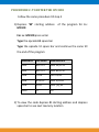
4.7 T (Transfer Command)
Example:
Press ‘T ‘
The source segment addresses 0000. The above command
transfer the memory content starting from source start address
1100 to destination start address 1200 till source end address
1500 is reached.
Src seg address
0000
Starting address
1100
End address
1200
Destination
1500
address
Block
Transfer
Src
0000
Enter Key
seg
:
start : 1100
Enter the 1100 address
end : 1200
Enter the 1200address
Enter Key
for exit command
dest :
0 :
1500
Enter Key
Transfer
Complete
Enter Key
for exit command
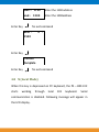
4.8 N (Local Mode)
When this key is depressed on PC keyboard, the PS – 8051 Kit
starts
working
through
local
101
keyboard.
Serial
communication is disabled. Following message will appear in
the LCD display.
!
NORMAL
MODE !
4.9 B (baud rate)
Press the ‘B ‘
Cur
BAUD :
2400
Enter the Space Bar Key
150
Cur BAUD :
2400
9600
Enter Key
SET the 9600 baud rate
Baud rates : 150, 300, 600, 1200, 2400, 4800, 9600
When using the serial Communication.
4.10
S (Serial Mode Key)
When this key is depressed the system start communicating
through connector.
All keys are disabled except reset.
! Serial Mode!
The system displays the message SERIAL MODE. To come back
to LCD mode (Normal Mode) user has to press the ‘N’ key in the
computer keyboard otherwise press the Reset button.
4.11
Programming The 8086 Trainer Kit:
PROCEDURE 1: TO ENTER THE MNEMONICS
1) Initially connect the 9V adaptor to J10 connector
2) Switch ON the PS-8086 kit using slide Switch SW1
3) “PS - 86” will be displayed on the LCD
4) Connect the Keyboard in PS/2 connector
5) Depress “A” starting address of the program for Ex: A1100
For ex: A1100 enter key
Type the mnemonics MOV AX, 1212press Enter key
Type the mnemonics MOV BX, 1212 press Enter key and
continue the same procedure till the end of the program
ADDRESS
OPCODES
MNEMONICS
1100
B8 12 12
MOV AX,1212
1103
BB 12 12
MOV BX,1212
1106
01 D8
ADD AX,BX
1108
BE 00 12
MOV SI,1200
110B
89 04
MOV [SI],AX
110D
F4
HLT
6) To verify the code depress D starting address and depress
space bar to see next memory location
For Ex: D1100 and press spacebar till the end of the
program
7) To execute the program Depress “G staring address for Ex:
G1100.
8) To see the result depress “M result address” for Ex:
M1200.
9) To view the output in the Register depress ‘R’ and press
enter key in keyboard.
PROCEDURE 2: TO ENTER THE OPCODE
Follow the same procedure till step 4
1) Depress “M” starting address
M1100
of the program for Ex:
For ex: M1100 press enter
Type the opcode B8 space bar
Type the opcode 12 space bar and continue the same till
the end of the program
ADDRESS
OPCODES
MNEMONICS
1100
B8 12 12
MOV AX,1212
1103
BB 12 12
MOV BX,1212
1106
01 D8
ADD AX,BX
1108
BE 00 12
MOV SI,1200
110B
89 04
MOV [SI],AX
110D
F4
HLT
2) To view the code depress D starting address and depress
space bar to see next memory location
For Ex: D1100 and press spacebar till the end of the
program
3) To execute the program Depress “G staring address for Ex:
G1100.
4) To see the result depress “M result address” for Ex:
M1200.
5) To view the output in the Register depress ‘R’ and press
enter key in keyboard
Note: 1) “M” is used for displaying the result, for Ex: M8500
2) “M” is used to entering the Opcode.
3) “M” is used for entering the data.
Note: There are two ways to enter the program
1) Mnemonics method
2) Opcode method
Sample program is given to enter the program in both the
methods
CHAPTER – 5 PROGRAMMING DETAILS
PROGRAMMING 8086 OVERVIEW
The 8086 Microprocessor uses a multiplexed 16 bit address
and address bus
During the first clock of machine cycle the 16 bit address s
sent out on address/data bus
These 16 bit addresses may be latched externally by the
address latch enable signals(ALE)
8086 Microprocessor can access 1024kb of external
memory using its 20 bit address and memory read/write
signals
The 8086 provide s0, s1 and s2 signals for bus control.
The 8086 Microprocessor has a 16 bit program counter (IP)
and 16 bit stack pointer (sp)
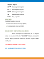
It has following set of 16 bit Registers:
AX –Accumulator
BX, CX, DX
(These four register can be used as two 8 bit
register individually)
Index Register
SI
Source index
DI
Destination index
BP
Base pointer index
Segment Register
CS
Code segment register
DS
Data segment register
ES
Extra segment register
SS
Stack segment register
FL
Flag register
Interrupts:
The 8086 have two interrupt
External mask able interrupt (INTR)
Non mask able interrupt (NMI)
BREAK POINT DISPLAY IN LOCAL MODE:
When break point is encountered, all the register
values are saved and the Acc. “AX=XXXX “Value is displayed in
the LCD display. Now use SPACE key to check register values
one by one
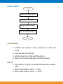
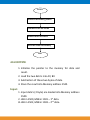
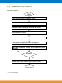
CHAPTER 6: EXAMPLE PROGRAMS
6.1 Addition Of Two Bytes Of Data
FLOW CHART:
START
Initialize the Memory pointer
Load data to AX and BX
Add two data of AX and BX
Store the result into Memory
EXIT
ALGORITHM:
1. Initialize the pointer to the memory for data and
result.
2. Load the data into AX, BX.
3. Add the two data of AX and BX registers.
4. Store the result into Memory from AX registers.
INPUT:
1. Input data’s (2 byte) are loaded into Memory address
1500.
2. LSB in 1500, MSB in 1501 – 1st data.
3. LSB in 1502, MSB in 1503 – 2nd data.
Output:
1. Result stored in Memory address 1520.
2. LSB in 1520, MSB in 1521.
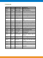
Program
ADDRESS OPCODE MNEMONICS COMMENTS
1100
BE 00 15
MOV
1500
LODSW
MOV
AX
LODSW
SI,
Move 1500 into SI pointer
1103
1104
AD
89 C3
BX,
Load the first data into AX
Move AX value into BX
1106
AD
1107
1109
01 C3
BF 20 15
110C
89 1D
ADD BX, AX
MOV
DI,
1520
MOV [DI], BX
110E
74
HLT
Load the second data into
AX
Add BX and AX registers
Load
1520
address
location into DI
Store BX value into
memory
HALT
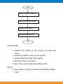
6.2 SUBTRACTION OF TWO BYTES OF DATA
FLOW CHART:
START
Initialize the Memory pointer
Load data’s into AX and BX
Subtract these two data’s
Store the result into Memory
END
ALGORITHM:
1. Initialize the pointer to the memory for data and
result.
2. Load the two data’s into AX, BX.
3. Subtraction of these two bytes of data.
4. Store the result into Memory address 1520.
Input:
1. Input data’s (2 byte) are loaded into Memory address
1500.
2. LSB in 1500, MSB in 1501 – 1st data.
3. LSB in 1502, MSB in 1503 – 2nd data.
OUTPUT:
1. Result stored in Memory address 1520.
2. LSB in 1520, MSB in 1521.
Program:
ADDRESS OPCODE MNEMONICS COMMENTS
1100
BE 00 15
MOV SI,1500
Load 1500 into SI
1103
AD
LODSW
Load the first data
1104
89 C3
MOV BX, AX
Move AX value into BX
1106
AD
LODSW
Load the second data
1107
01 C3
SUB BX, AX
subtract AX from BX
1109
BF 20 15
MOV DI, 1520 Load 1520 address into DI
110C
89 1D
MOV [DI],BX
Load BX value into DI
110E
CC
INT 3
Break point
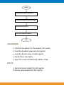
6.3 MULTIPLICATION OF TWO BYTE DATA
FLOW CHART:
START
Initialize the Memory pointer SI
Load the two data’s into AX, BX
Multiply of these two data’s
Store the result into Memory
END
ALGORITHM:
1. Initialize the pointer to the memory for data and
result.
2. Load the multiplier value into AX register.
3. Load multiplicand value in BX register.
4. Multiply of these two data’s.
5. Store the result into Memory address 1520.
INPUT:
4. Input data’s (2 byte) are loaded into Memory address
1500.
5. Load the multiplier value in 1500.
6. Load the multiplicand value in 1502.
OUTPUT:
1. Result stored in Memory address 1520.
Program:
ADDRESS
1100
1103
1104
1106
1107
1109
110C
110E
110F
1110
1112
OPCODE
BE 00 15
AD
89 C3
AD
F7 E3
BF 0 5 15
89 05
47
47
89 15
CC
MNEMONICS
MOV SI,1500
LODSW
MOV BX, AX
LODSW
MUL BX
MOV DI, 1520
MOV [DI], AX
INC DI
INC DI
MOV [DI], BX
INT 3
6.4 DIVISION (2 BYTE/ 1 BYTE)
FLOW CHART:
COMMENTS
Load 1500 into SI
Load the multiplicand value
Load AX value into BX
Load the multiplier value
Multiply two data
Load 1520 address into DI
Store AX value into DI
Increment the DI
Increment the DI
Store BX value into DI
Break point
START
Initialize the Memory pointer SI
Load the dividend and divisor values
Divide these two data’s
Store the result into Memory
EXIT
ALGORITHM:
1. Initialize the pointer to the memory for result.
2. Load the dividend value into AX register.
3. Load the divisor value into BX register.
4. Divide these two data’s.
5. Store the result into Memory address 1520.
INPUT:
1. Dividend value loaded into AX register.
2. Divisor value loaded into BX register.
Output:
1. Result stored into 1520 address.
2. Quotient stored into 1522 address.
3. Remainder stored into 1523 address.
Program:
ADDRESS OPCODE MNEMONICS
COMMENTS
1100
BA 00 00
MOV DX, 0000
Clear DX registers
1103
B8 FD FF
MOV AX, FFFD
Load the dividend in AX
1106
B9 0F 00
MOV BX, 0F
Load the divisor value in BX
1109
F7 F1
DIV BX
Divide the two data’s
110B
BF 00 15
MOV DI, 1520
Load 1520 address into DI
110E
88 05
MOV [DI], AL
Load AL value into DI
1110
47
INC DI
Increment DI
1111
88 25
MOV [DI], AH
Load AH value into DI
1113
1114
47
89 15
INC DI
MOV [DI], DX
Increment DI
Load DX value into DI
1116
CC
INT3
Break point
6.5 BLOCK MOVE FROM ONE LOCATION TO ANOTHER
FLOW CHART:
START
Initialize the memory pointer
CL = No of count loaded into AL
Transfer data to the desired location
CL = CL - 1
Load next data in AL
NO
If
CL=0
YES
Store the result into Memory
EXIT
ALGORITHM:
1. Initialize the pointer to the memory where data to be
transformed.
2. Load the AL register with the data from memory.
3. Initialize destination pointer to the memory where
data to stored.
4. Store data from AL register.
INPUT:
Input data from address 1500 which is pointed SI,
transferred to the desired Location.
Number of byte in CL.
Output:
Output – data in address 1550 is the moved data.
PROGRAM:
ADDRESS OPCODE MNEMONICS
COMMENTS
1100
B1 08
MOV CL, 08
Load 08 value into CL
1102
BE 00 14
MOV SI, 1500
Load 1500 into SI
1105
BF 50 14
MOV DI, 1550
Load 1550 into DI
1108
AC
LODSB
Load the data in AL Register
1109
88 05
MOV [DI], AL
110B
47
INC DI
Store the result in specified
Location
Increment the pointer
110C
FE C9
DEC CL
Decrement the pointer
110E
75 F8
JNZ 1108
1110
CC
INT 3
Loop continues until the counter
is zero
Break point
6.6 SEARCHING A BYTE
Flow Chart:
START
Initialize the memory pointer
CL = Count
DL = search byte
Load the data into AL register
NO
CL = CL - 1
If AL = DL
YES
Store searched byte & location
EXIT
Algorithm:
1. Initialize the pointer to the memory for storing data
and result.
2. Load DL with search byte.
3. Load CL with count.
4. Load AL with data from memory. Compare AL with DL
if its equal store the result else decrement counts go
to step2.
5. Store the result.
INPUT:
1. (Search the byte) A in 50 locations from 1500.
Output:
1. Store the result byte in 1600.
PROGRAM:
ADDRESS
1100
1103
1106
1108
110A
110B
OPCODE
BF 00 13
BE 00 12
B1 50
B2 0A
AC
38 C2
MNEMONICS
MOV DI, 1600
MOV SI, 1500
MOV CL, 50
MOV DL, 0A
LODSW
CMP DL, AL
110D
110F
FE C9
75 05
DEC CL
JZ 1114
1111
75 F7
JNZ 110A
1113
1114
F4
88 05
HLT
MOV [DI], AL
COMMENTS
Load 1600 into DI
Load 1500 into SI
Load 50 into CL
Load 10 into DL
Load CL register with the count
Compare DL and AL register
values
Decrement CL register
If count is zero then jump into
1114
If count is not zero then jump
into 110A
Load AL value into DI
1116
1117
1119
111A
111C
111D
111F
4E
89 F3
47
88 1D
47
88 3D
CC
DEC SI
MOV BX, SI
INC DI
MOV [DI], BL
INC DI
MOV [DI], BH
INT 3
Decrement SI register
Load SI value into BX
Increment DI
Store BL value into DI
Increment DI
Store BH value into DI
Break point
6.7 GRAY CODE CONVERSION (Look Up Table)
Flow Chart:
START
Initialize the memory pointer
Load data into AL register
Convert AL into gray code
Store the result into Memory
EXIT
ALGORITHM:
1. Load the memory with truth table of gray codes.
2. Initialize the pointer to the memory for data and
result.
3. Load AL with the data from memory.
4. Convert gray code for that data.
5. Store the result into Memory.
INPUT
: Data in 1500.
OUTPUT
: Result in 1501.
Lookup Table
: Start from 1600.
The look up table is provided by hex or of two bits in a byte
the value ranges from 00 to 0f. 1600 - 00 01 03 02 06 07 05 04
0c 0d 0f 0e 0a 0b 09 08.
Program:
ADDRE OPCODE
SS
1100
BB 00 12
MNEMONIC COMMENTS
S
MOV
BX, Load 1200 into BX
1600
1103
BE 50 11
MOV SI, 1500 Load 1500 into SI
1106
AC
LODSB
Load the accumulator with the data
1107
D7
XLAT
Check gray code for that data
1108
BF 51 11
110B
88 05
110D
CC
MOV
DI, Load 1501 address into DI
1501
MOV [DI], AL Store the gray code of the given
data
INT3
Break point
6.8 SUM OF N CONSECUTIVE NUMBERS
FLOW CHART:
START
Initialize the memory pointer SI
Load the data as BL = 1, CL = count
T (n) = t (n - 1) + t (n - 2). BL = BL + 1. AL = t (n).
NO
If CL = 0
YES
Store the result into Memory address 1600
EXIT
ALGORITHM:
1. Load the value of n.
2. t (n) = t (n - 1) + t (n - 2).
3. t (n - 1) = t (n - 2) + 1.
4.
5.
6.
7.
n = n - 1.
if n > 0 continue else go to step2.
Initialize the pointer to memory for storing the result.
Store result.
INPUT
: Load the value of n into CL.
OUTPUT : Result is stored in 1600.
PROGRAM:
ADDRESS
1100
1102
1104
1106
1108
110A
110C
OPCODE
B1 O4
B0 00
B3 01
00 D8
FE C3
FE C9
75 F8
110E
1111
1113
BF 00 20
89 05
CC
MNEMONICS
MOV CL,04
MOV AL,00
MOV BL,01
ADD AL,BL
INC BL
DEC CL
JNZ 1106
COMMENTS
Load CL with value 04
Initialize 00 value into AL
Initialize 01 value into BL
Add previous and next value
Increment BL
Decrement CL
Loop executes until the
desired value of n is reached
MOV DI,1600 Store the result in 1600
MOV [DI],AX Load AX value into DI
INT3
Break point
6.9 ASCII TO HEX CODE CONVERSION
FLOW CHART:
START
Load AL with the input data
Subtract AL with 30HEX
NO
If
AL<=10
YES
AL = AL - 7
EXIT
Algorithm:
1. Load the input data in AL register.
2. Subtract 30 from AL register value.
3. If data is less than or equal to 16 terminate the
program.
4. Else subtract 7 from AL register value.
5. Result stored in AL register.
INPUT
:
Data input in AL register.
OUTPUT
:
Data output in AL register.
PROGRAM:
ADDRESS OPCODE MNEMONICS COMMENTS
1100
B0 31
MOV AL,31
Get data 31 into AL
1102
2C 30
SUB AL,30
Subtract 30 with the AL
1104
3C 10
CMP AL,10
1106
72 04
JB 110C
1108
74 02
JZ 110C
If data is less than or equal to 16 go to
110C
If 1st operand is below the 2nd
operand then short jump into 110C
If count zero then jump into to 110C
110A
2C 07
SUB AL,07
Else subtract 7 from AL register value
110C
CC
INT 3
Break point
6.10 BCD TO HEXA DECIMAL CONVERSION
FLOW CHART:
START
Load at with the data mask higher, lower bits
Multiply by 10 and add lower bits to it
Move higher bits into lower bits
EXIT
ALGORITHM:
1. Load the data in AL register.
2. Separate higher nibbles and (in) lower nibbles.
3. Move the higher nibbles (in) to lower nibbles position.
4. Multiply AL by 10.
5. Add lower nibbles.
6. Store the result into Memory.
INPUT:
Data in AL register.
OUTPUT:
Result in AL register.
PROGRAM:
ADDRESS
1100
1102
1104
1107
1109
110B
110D
OPCODE
B0 10
88 C4
80 E4 OF
88 E3
24 F0
B1 O4
D2 C8
MNEMONICS
MOV AL,10
MOV AH,AL
AND AH,0F
MOV BL,AH
AND AL,F0
MOV CL,04
ROR AL,CL
110F
1111
1113
B7 0A
F6 E7
00 D8
MOV BH,0A
MUL BH
ADD AL,BL
1115
CC
INT3
COMMENTS
Load register AL with the data 10
Load AL value into AH
Mask higher bits
Load AH value into BL
Mask lower bits
Load 04 value into CL
Rotate the data from last 4bits
to first 4 bits
Load 10 value into BH
Multiply by 10
Add lower nibble to the
multiplied data
Break point
6.11 HEXA DECIMAL TO ASCII CODE
FLOW CHART:
START
Load AL register with the input data
YES
If AL<=9
AL = AL + 7
NO
Add AL register with 30
Store the result into Memory
EXIT
ALGORITHM:
1. Load AL with the input data.
2. Check If (AL<=9) then add 30 with AL register.
3. Else add 7 with AL register.
4. Result stored into AL register.
INPUT:
Data in AL register.
OUTPUT:
Result in AL register.
PROGRAM:
ADDRESS OPCODE MNEMONICS COMMENTS
1100
B0 0A
MOV AL,0A
1102
3C 09
CMP AL,09
1104
1106
74 04
72 02
JZ 110A
JB 110A
1108
110A
110C
04 07
04 30
CC
ADD AL,07
ADD AL,30
INT3
6.12 MATRIX ADDITION
FLOW CHART:
Load register AL with the data
10
If data less than 9 add 30 to
the data
If count is zero then go to 110A
If 1st operand is below than 2nd
operand then short jump into
110A
Else Add AL with 07
add 30 with AL
Break point
START
Initialize memory pointer for the two matrix SI and DI
Load the input data’s into CL = Count, AL = data
Add AL register with BL register
Store the result into Memory
Decrement the count value in CL register
NO
If CL=0
YES
EXIT
ALGORITHM:
1. Initialize the pointer to memory for data and result.
2. Load CL with count.
3. Add two matrices by each element.
4. Process continues until CL is 0.
5.Store the result into Memory.
INPUT:
Data in 2000 consecutive location as rows and
columns for first matrix.
Data in 3000 consecutive location as rows and
columns for second matrix.
OUTPUT:
Data in 3000 with 9 entries.
PROGRAM:
ADDRESS OPCODE MNEMONICS COMMENTS
1100
B1 09
MOV CL, 09
Initialize 09 into CL register
1102
BE 00 20 MOV SI, 2000 Load 2000 into SI for 1st
matrix
1105
BF 00 30 MOV DI, 3000 Load 3000 into DI for 2nd
matrix
1108
8A 04
MOV AL, [SI] Load AL with data of first
matrix
110A
8A 1D
MOV BL, [DI] Load BL with data of second
matrix
110C
00 D8
ADD AL, BL
Add two data of AL and BL
110E
88 05
MOV [DI], AL Store AL with data into DI
1110
47
INC DI
Increment DI
1111
46
INC SI
Increment SI
1112
FE C9
DEC CL
Decrement CL
1114
75 F2
JNZ 1108
Loop continues until all
elements of
Matrix to added
1116
CC
INT3
Break point
6.13 SEPERATING ODD AND EVEN
FLOW CHART:
START
Initialize the memory pointer
memort
Load the data in AL register
Rotate the data in AL register
YES
If carry set
Store the result
NO
NO
CL = CL - 1
CL = 0?
YES
EXIT
ALGORITHM:
1. Initialize the pointer to memory for data and result.
2. Loaded the data in AL register from memory.
3. Rotate the AL register by one bit.
4. If carry flag is set then go to step2.
5. Store the even number as a result into the Memory.
INPUT:
Data in 2000 (mixer of odd and even numbers).
Count: number of bytes in CL.
OUTPUT:
Even numbers stored in 3000.
PROGRAM:
ADDRESS
1100
1102
1105
1108
1109
110B
OPCODE
B1 08
BE 00 20
BF 00 30
AC
D0 C8
72 FB
110D
D0 C0
110F
1111
1112
1114
88 05
47
FE C9
75 F2
1116
CC
MNEMONICS
MOV CL, 08
MOV SI, 2000
MOV DI, 3000
LODSB
ROR AL,1
JB 1108
COMMENTS
Initialize 08 into CL
Load 2000 address into SI
Load 3000 address into DI
Load the counter value
Rotate AL in one time
If carry occurs go to L1 (odd
Data)
ROL AL, 1
Else rotate by left to get
original data
MOV [D1], AL Store the even data
INC DI
Increment DI
DEC CL
Decrement CL
JNZ 1108
Loop executes until counter is
zero
INT3
Break point
6.14 FIBONACCI SERIES
FLOEW CHART:
START
Initialize the memory pointer SI
Load data in BL = t (n - 1), AL = t (n) CL=count
T (n + 1) = t (n - 1) + t (n)
Decrement the CL register by one time
NO
If CL = 0
YES
Store the result into Memory address 2000
EXIT
ALGORITHM:
1. Initialize the pointer to memory for storing result.
2. Number of the counts loaded into CL register.
3. T (n + 1) = t (n) + t (n - 1).
4. Repeat the above process until count is 0.
INPUT:
Load number of terms in CL.
OUTPUT:
Result in 2000 (clear the memory from 2000 by
00 before executing the program).
PROGRAM:
ADDRESS
1100
1102
1104
1106
1109
110B
110D
110F
1110
1112
1114
1116
OPCODE
B1 10
B3 00
B2 01
BF 00 20
88 D0
00 D8
88 05
47
88 D3
88 C2
FE C9
75 F3
MNEMONICS
MOV CL, 10
MOV BL, 00
MOV DL, 01
MOV DI, 2000
MOV AL, DL
ADD AL, BL
MOV [DI],AL
INC DI
MOV BL, DL
MOV DL, AL
DEC CL
JNZ110B
1118
CC
INT3
COMMENTS
Initialize 10 into CL register
Initialize 00 into BL register
Initialize 01 into DL register
Load 2000 into DI
Move DL value into AL
Add BL value with AL register
Store AL value into DI.
Increment DI
Move DL value BL register
Move AL value DL register
Decrement CL
If count is zero then go to
110B
Breakpoint
6.15 FACTORIAL OF A NUMBER
FLOW CHART:
START
Initialize the memory pointer SI
Load data in BL = l, AL = l, CL = count
T(n - 1) = (n - 1) * t(n). BL = BL + l
Decrement the CL register value
NO
If CL=0
YES
Store the result into Memory address 2000
END
n!=n*(n-1)*(n-2)*…………..*1
ALGORITHM:
1. Load the counter with value of n into CL register.
2. T (n) = t (n - 1) * t (n - 2).
3. Repeat the process until n becomes to store result.
4. Initialize the pointer to memory to store result.
5. Store the result into Memory address 2000.
INPUT:
Load the value of n into CL register.
OUTPUT:
Result stored in Memory address 2000.
PROGRAM:
ADDRESS
1100
1102
1104
1106
OPCODE
B1 04
B0 01
B3 01
F6 E3
MNEMONICS
MOV CL, 04
MOV AL, 01
MOV BL, 01
MUL BL
COMMENTS
Load the value of 04 in CL
Initialize 01 into AL
Initialize 01 into BL
Multiply previous value by next
Value
Increment BL
1108
FE C3
INC BL
110A
110C
FE C9
75 F8
DEC CL
JNZ 1106
110E
BF 00 20
Decrement CL
Loop continues until count is
Zero
MOV DI, 2000 Load 2000 address into DI
1111
1113
89 05
CC
MOV [DI], AX
INT3
Store AX value into DI
Break point
6.16 FIND THE LARGEST NUMBER IN AN ARRAY
START
Move the start address to a memory pointer
Initialize the counter with number of elements in array
Move the data pointed by the memory to register1
Increment the memory pointer SI
Decrement the counter in CL register
Compare reg1 data
with data pointed by
the memory
NO
YES
Is
register1
data greater?
Store the data
NO
Is count=0?
YES
EXIT
e
nd
ALGORITHM:
1. Take the first number of the array.
2. Compare with next number.
3. Take the bigger one of the them.
4. Decrement the count in CL register.
5. If the count is not zero then continue from step 2.
6. Store the result into Memory address 9500.
INPUT:
Enter the size of array (count) in 9000.
Enter the data starting from 9001.
OUTPUT:
Result is stored in 9500.
PROGRAM:
ADDRESS
1100
1103
1105
1106
1108
110A
110B
110D
110F
1111
1113
OPCODE
BE 00 90
8A 0C
46
8A 04
FE C9
46
3A 04
73 02
8A 04
FE C9
75 F5
MNEMONICS
MOV SI,9000
MOV CL,[SI]
INC SI
MOV AL,[SI]
DEC CL
INC SI
CMP AL,[SI]
JNB 1111
MOV AL,[SI]
DEC CL
JNZ 110A
1115
1118
111A
BF 00 95
88 05
CC
MOV DI,9500
MOV [DI],AL
INT3
COMMENTS
Load 9000 address into SI
Load SI value into CL
Increment SI
Move the first data in AL
Reduce the count
Increment SI
if AL> [SI] then go to jump1 (no swap)
If count is zero then jump into 1111
Else store large no in to AL
Decrement the count
If count is not zero then jump into
110A
Else store the biggest number at 9500
Store the AL value into DI
Break point
6.17 AVERAGE OF AN ARRAY
FLOW CHART:
START
Move the start address to a memory pointer
Initialize register1 with zero
Initialize counter with number of elements in an array
Save the count in register3
Move the data from the memory pointer address to register2
Add register1 to register2 and store into register1
Increment the memory pointer & Decrement the counter
ercounter
NO
Is count=0?
YES
Divide register3 from register2 and store into register2
EXIT
ALGORITHM:
1. Add the bytes one by one up to the count (CL).
2. Then divide the total with the count.
INPUT:
Size of array (count) in CL = 6 (see the program).
Enter the data starting from 9000h.
OUTPUT:
Average is stored in AX register.
Quotient in AL and the reminder in AH.
PROGRAM:
ADDRESS OPCODE
MNEMONICS COMMENTS
1100
BB 00 00
MOV BX,0000 Load 0000 into BX
1103
BE 00 90
MOV SI,9000
1106
B8 00 00
MOV AX,0000 Load 0000 into AX
1109
B1 06
MOV CL,06
Initialize 06 into CL register
110B
88 CD
MOV CH,CL
Load the count value into CH
110D
8A 1C
MOV BL,[SI]
Get the data byte
110F
00 D8
ADD AL,BL
Add the data byte
1111
46
INC SI
Increment the SI pointer
1112
FE C9
DEC CL
Check the count
1114
75 F7
JNZ 110D
1116
F6 F5
DIV CH
If count is not zero then go to
110D
Find the average by sum/count
1118
CC
INT3
Break point
Array start address
6.18 GENERATE SQUARE WAVE
I/O ADDRESS FOR 8253 /8254:
Counter 0 FF00
Counter 1 FF02
Counter 2 FF04
Counter reg FF06
FLOW CHART:
START
Initialize 8253 with counter2 in mode 3
Load data ‘FF’ in LSB of counter2
Load data ‘00’ in MSB of counter2
STOP
PROGRAM:
ADDRESS OPCODE MNEMONICS
COMMENTS
1100
B0 B7
MOV AL,36
1102
BA 06 FF
MOV DX,FF06
Load 36 into AL for generating
SQUARE
Load FF06 into DX
1105
EE
OUT DX,AL
Send the data to the timer
1106
B0 02
MOV AL,FF
Load LSB count in the AL
1108
BA 04 FF
MOV DX,FF04
Port address in DX
110B
EE
OUT DX,AL
Output the AL contents to CLK 2
110C
B0 00
MOV AL,00
Load MSB count in the AL
110E
BA 04 FF
MOV DX,FF04
Load FF04 into DX
1111
EE
OUT DX,AL
Output the AL content to CLK 2
1112
CC
INT3
Break point
6.19 DESCENDING ORDER
ALGORITHM:
1. Get the first data and compare with the second data.
2. If the two data are in descending order then no swap.
3. Else swap the data byte by descending order and then
again compare the other data bytes up to the count.
4. Do the above the array is a ranged in descending order.
5. Finally the array is arranged in ascending order.
INPUT:
Enter the count in location 9000.
Enter the data location starting from 9001.
OUTPUT:
Result in descending order in the location 9001.
FLOW CHART:
START
Load the counter with the number of elements in the array
Move the data from the memory pointer to a register 1
Increment the memory pointer SI
Move the subsequent data to register 2
NO
Swap reg1 & reg2
Is
reg1<reg2?
YES
Increment the memory pointer
Store reg1 data to memory pointer address
Increment the memory pointer
Decrement the counter in one time
NO
Is Count = 0?
YES
EXIT
PROGRAM:
ADDRESS
1100
1103
1105
1108
110A
110B
110D
110F
OPCODE
BE 00 90
8A 0C
BE 00 90
8A 14
46
8A 04
FE CA
74 16
MNEMONICS
MOV SI, 9001
MOV CL, [SI]
MOV SI, 9000
MOV DL, [SI]
INC SI
MOV AL, [SI]
DEC DL
JZ 1127
1111
1112
1114
1116
1118
1119
111B
111D
111F
1120
46
8A 1C
3A C3
72 07
4E
88 04
88 D8
EB 03
4E
88 1C
INC SI
MOV BL, [SI]
CMP AL, BL
JB 111F
DEC SI
MOV [SI],AL
MOV AL, BL
JMP 1122
DEC SI
MOV [SI], BL
1122
1123
1125
46
FE CA
75 EA
INC SI
DEC DL
JNZ 1111
1127
1129
112B
88 04
FE C9
75 D8
MOV [SI], AL
DEC CL
JNZ 1105
112D
CC
INT3
COMMENTS
Load 9000 into SI
Load SI value into CL
get the count
Load SI count value into DL
Increment the pointer
first data in AL
Decrement DL
If count is zero then jump into
1127
Increment SI
Load SI count value into BL
if al > bl go to (jump1)
Decrement SI
Load ACC value in SI
Store the greatest data
Jump into 1122
Decrement SI
Store the smallest data in
memory
Increment SI
Decrement DL
If count is not zero then jump
into 1111
Load AL value into SI
Decrement CL
If count is not zero then jump
into 1105
Break point
6.20 ASCENDING ORDER
ALGORITHM:
1. Get the first data and compare with the second data.
2. If the two data are in ascending order then no swap.
3. Else swap the data byte by ascending order and then
again compare the other data bytes up to the count.
4. Do the above the array is arranged in ascending order.
5. Finally the array is arranged in ascending order.
INPUT:
Enter the count in location 9000.
Enter the data location starting from 9001.
OUTPUT:
Result in ascending order in the location 9001.
FLOW CHART:
START
Load the counter with the number of elements in the array
Move the data from the memory pointer to a register 1
Increment the memory pointer SI
Move the subsequent data to register 2
NO
If
reg1>reg2?
Swap reg1 & reg2
YES
Increment the memory pointer SI
Store register1 data to memory pointer address
Increment the memory pointer SI
Decrement the counter value
NO
Is
Count=0?
YES
EXIT
PROGRAM:
ADDRESS
1100
1103
1105
1108
OPCODE
BE 00 90
8A 0C
BE 00 90
8A 14
MNEMONICS
MOV SI, 9000
MOV CL, [SI]
MOV SI, 9000
MOV DL, [SI]
110A
110B
110D
110F
46
8A 04
FE CA
74 16
INC SI
MOV AL, [SI]
DEC DL
JZ 1127
1111
1112
1114
1116
1118
1119
111B
111D
111F
1120
1122
1123
1125
46
8A 1C
38 D8
72 07
4E
88 04
88 D8
EB 03
4E
88 1C
46
FE CA
75 EA
INC SI
MOV BL, [SI]
CMP AL, BL
JNB 111F
DEC SI
MOV [SI],AL
MOV AL, BL
JMP 1122
DEC SI
MOV [SI], BL
INC SI
DEC DL
JNZ 1111
1127
1129
112B
88 04
FE C9
75 D8
MOV [SI], AL
DEC CL
JNZ 1105
112D
CC
INT3
COMMENTS
Load 9000 into SI
Load SI value into CL
Get second data
Load SI second data into
DL
Increment SI
Load SI value into AL
Decrement DL
If count is zero then go
to 1127
Increment SI
Load SI value into BL
if AL > BL go to (jump1)
Decrement SI
Load AL value into SI
Load BL value into AL
Decrement SI
Load BL value into SI
Increment SI
Decrement DL
If count is not zero then
go to 1111
Load AL value into SI
Decrement CL
If count is not zero then
go to 1105
Breakpoint
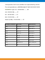
ADDITIONAL PROGRAMS ON 8086
1)
COMPARE STRING
ADDRESS MNEMONICS
1100
LEA SI, [1200]
1104
LEA DI, [1300]
1108
MOV CX, 0003H
110b
CLD
110c
REPE CMPSB
110e
JNZ NOTEQUAL
1110
MOV AL, 01
1112
MOV [1400], AL
1115
HLT
1116
NOTEQUAL:
MOV
AL, 00
1118
MOV [1400], AL
111b
HLT
CONDITION 1: (SAME STRING IN DATA1 AND DATA2)
1ST INPUT
2ND INPUT
1200
11
1300
11
1201
22
1301
22
1202
33
1302
33
OUTPUT: 1400 : 01
CONDITION 2: (DIFFERENT STRING IN DATA1 AND
DATA2)
1ST INPUT
2ND INPUT
1200
11
1300
44
1201
22
1301
55
1202
33
1302
66
OUTPUT:
2)
1400 :
MOV STRING PROGRAM
ADDRESS
1100
OPCODE
MOVCX,[1500]
1104
LEA
SI,[1600]
1108
LEA
DI,[1700]
110c
CLD
110d
REP
110f
HLT
MOVSB
INPUT LOCATION
COUNT INPUT
DATA INPUT
1500
03
1601
22
1601
11
1602
33
OUT LOCATION
OUTPUT
1700
11
1701
22
1703
33
3)
ONE'S COMPLEMENT OF A 16-BIT NUMBER
OBJECTIVE:
To find the one's complement of the data in register pair AX and
store the result at 1400.
THEORY:
In the one's complement of a binary number the ones are
changed to zeros and vice versa. It is one way of representing
negative numbers. All negative numbers start with a 1 at the
MSBit. For instance considering the hex number 5600 For ex:
5600 = 0101 0110 0000 0000
One's complement = 1010 1001 1111 1111
= A9FF
EXAMPLE:
The example given is to find the one's complement of 1234 and
store it in memory location 1400.
Input :
Data: (AX) = 0001 0010 0011 0100 = 1234
Result: [1400] = 1110 1101 1100 1011 = EDCB
MEMORY ADDRESS
OPCODE
MNEMONICS
1100
C7 C0 34 12
MOVAX, 1234
1103
F7 D0
NOT AX
1106
89 06 00 14
MOV [1400],AX
110A
F4
HLT
PROCEDURE
i) Enter the above mnemonics into RAM memory from 1100
using the assembler command.
ii) Using GO command execute the program and enter 1100.
This is the address from where execution of your program
starts.
iii) Press ENTER key to start execution.
iv) Reset the kit using RESET key.
4)
MASKING OFF BITS SELECTIVELY
OBJECTIVE
To clear 8 selected bits, the 2nd HN and the HN in a 16 bit number.
THEORY
The logical AND instruction is used for masking off bits. The bits
which have to be cleared are to be AND with a logical zero and the
other bits are to be high. Hence to achieve the above objective,
AND with 0F0F.
EXAMPLE: The 16 bit number is at location 1200 and the result
is at location 1400.
Input: [1200] = FF
[1201] = FF
Result: [1400] = 0F
[1401] = 0F
MEMORY ADDRESS
OPCODE
MNEMONICS
1100
8B 06 00 12
MOV BX,1200
1104
81 E0 0F0F
AND AX,0F0F
1108
89 06 00 14
MOV [1400],AX
110C
F4
HLT
PROCEDURE
The procedure outlined for previous exercises is to be followed
for this program also.
5)
COMPUTING A BOOLEAN EXPRESSION
OBJECTIVE
To obtain a Boolean expression F which has 4 terms and 8
variables A,B,C,D,E,F,G,H. F = {(AB'CDE' + A'BCD(BCD+EFGH)}
THEORY
Evaluation of Boolean expressions through minimization
procedures is customary. But this example seeks to do the same
using the 8086 registers. The 4 minterms are in FOUR 8 bit
registers. Use of logical instructions to perform this is
consequential. Don't care variables are represented by set bits.
The correspondence is, ABCDEFGH)))) D7 D6 D5 D4 D3 D2 D1 D0
EXAMPLE: Input: AL = 10110111B ------- B7
AH = 01111111B ------ 7F
BL = 11111111B ------ FF
BH = 11111111B ------ FF
Result: [1100] = 11111111B ------ FF
MEMORY ADDRESS
OPCODE
MNEMONICS
1100
C6 C0 B7
MOV AL, B7
1103
C6 C4 7F
MOV AH, 7F
1106
C6 C3 FF
MOV BL, FF
1108
C6 C7 FF
MOV BH, FF
110C
08 FB
OR BL, BH
110E
20 DC
AND AH, BL
1110
08 E0
OR AL, AH
1112
88 06 00 12
MOV [1200], AL
1116
F4
HLT
Did you enjoy the read?
Pantech solutions creates information
packed technical documents like this one every
month. And our website is a rich and trusted
resource used by a vibrant online community of
more than 1,00,000 members from organization of
all shapes and sizes.
What do we sell?
Our
products
range
from
Various
Microcontroller development boards, DSP Boards,
FPGA/CPLD boards, Communication Kits, Power
electronics, Basic electronics, Robotics, Sensors,
Electronic components and much more . Our goal is
to make finding the parts and information you need
easier and affordable so you can create awesome
projects and training from Basic to Cutting edge
technology.