1
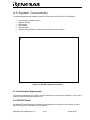
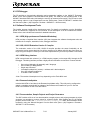
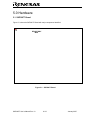
User
Powerful Processors – Easy to Use™
SKP36077
StarterKit Plus
User’s Manual
Rev. 1.0
January 2007
www.renesas.com
Table of Contents
1.0 Introduction ............................................................................................................................................. 3
2.0 Contents of Product Package................................................................................................................. 4
2.1. SKP36077 QuickStart Kit Item List.................................................................................................... 4
2.1.1. CD-ROM...................................................................................................................................... 4
3.0 Limited Guarantee and Support ............................................................................................................. 5
4.0 System Connectivity ............................................................................................................................... 6
4.1. Host Computer Requirements ........................................................................................................... 6
4.2. SKP36077 Board ............................................................................................................................... 6
4.3. E8 Debugger...................................................................................................................................... 7
4.4. Software Development Tools ............................................................................................................ 7
4.4.1. HEW (High-performance Embedded Workshop)........................................................................ 7
4.4.2. H8S, H8/300 Evaluation Version C Compiler............................................................................. 7
4.4.3. HEW Debug Interface ................................................................................................................. 7
4.4.4. Renesas AutoUpdater ................................................................................................................. 7
4.4.5. Documentation, Sample Projects and Project Generators ......................................................... 7
5.0 Hardware ................................................................................................................................................ 8
5.1. SKP36077 Board ............................................................................................................................... 8
5.2. SKP36077 Board Block Diagram ...................................................................................................... 9
5.3. SKP36077 Functional Blocks ............................................................................................................ 9
5.4. H8/36077 Group of MCUs ............................................................................................................... 10
5.5. LEDs ................................................................................................................................................ 10
5.6. SKP36077 Board Jumper Configuration ......................................................................................... 10
5.6.1. J10: LED D2 Drive Select.......................................................................................................... 10
5.6.2. P4: NMI Test............................................................................................................................ 10
5.6.3. Default Jumper Settings ............................................................................................................ 11
6.0 System Operation & Limitations ........................................................................................................... 12
6.1. Kernel (ROM Monitor) Introduction.................................................................................................. 12
6.2. Pin and Peripheral Limitations......................................................................................................... 12
6.3. Memory Map.................................................................................................................................... 12
6.4. Low Power Modes ........................................................................................................................... 13
6.5. Limitations on Interrupts .................................................................................................................. 13
6.6. Sleep Instruction Limitations............................................................................................................ 13
6.7. User Program’s Real-Time Capability ............................................................................................. 13
6.8. Watchdog Timer .............................................................................................................................. 14
7.0 SKP36077 Board Specifications........................................................................................................... 15
7.1. Hardware Specifications.................................................................................................................. 15
7.2. Power Supply Requirements ........................................................................................................... 15
7.3. Operating Environment.................................................................................................................... 15
Appendix A. Troubleshooting Guide........................................................................................................... 16
A.1 USB Driver Problems ....................................................................................................................... 16
A.2 Debugging Problems........................................................................................................................ 16
A.2.1 Erratic Debug Behavior.............................................................................................................. 16
A.2.2 Can’t Connect to Target............................................................................................................. 17
A.2.3 Issues that May Arise During Debug Operations ...................................................................... 17
Appendix B. Reference Manuals ................................................................................................................ 19
Appendix C. Expansion Headers................................................................................................................ 20
Appendix D. Board Schematic & BOM ....................................................................................................... 21
Appendix E. Other Resources .................................................................................................................... 22
SKP36077 User’s Manual Rev 1.0
January 2007
1.0 Introduction
The SKP36077 StarterKit Plus (SKP) is a low-cost development environment for evaluating the H8/300H
High Performance series of microcontrollers using the H8/36077 micro controller unit (MCU) and Renesas
software development tools.
The kit comes with a complete software development tool chain for Renesas MCUs, including Highperformance Embedded Workshop (HEW), which includes Integrated Development Environment (IDE),
Graphical User Interface (GUI) and Software Debugger; H8S-H8/300 C-compiler, assembler and linker;
and the E8 In-Circuit Debugger.
A real-time, source-level debug environment is implemented using the HEW4 software debug interface in
conjunction with the E8 hardware. The E8 also allows for programming H8/300 devices within HEW.
The E8 and firmware provide a convenient USB (Universal Serial Bus) interface between the SKP36077
board and the host PC. This interface reduces resource requirements on the H8/36077 MCU, allows
faster code downloads, and can be used with many other Renesas Flash MCUs, SKPs, and user target
boards.
SKP36077 User’s Manual Rev 1.0
3/ 22
January 2007
2.0 Contents of Product Package
This section describes the contents of the SKP36077 product package. When unpacking your SKP36077,
please check to see that all items listed below are included.
2.1. SKP36077 QuickStart Kit Item List
Table 2-1 lists the items included in the SKP36077.
Table 2-1 SKP36077 Item List
Item Name
SKP36077 Board
E8 Debugger
Quantity
1
1
6’ Mini USB Cable
SKP CD-ROM
1
1
Promotional CD
1
Remarks
US3664NEDK1 board
HEW Debugger/ USB Programmer Interface Device
(includes 14-pin ribbon cable)
Connects E8 Debugger to Host PC
Auto-install program
HEW (IDE & debugger)
H8S, H8/300 C-compiler, assembler, and linker
USB drivers
Manuals
Tutorials
Sample programs
Evaluation versions of third-party tools may be included
with the kit
2.1.1. CD-ROM
The CD-ROM contains the electronic manuals and software necessary for developing programs. Your
computer must have a web browser — like Mozilla Firefox, Netscape® Browser or Microsoft® Internet
Explorer — to view the help files, and Adobe® Acrobat® Reader® to view the manuals.
Insert the enclosed CD into your computer; the installer should auto-start. The installer program will
create C:\Renesas and C:\Workspace folders on your machine. Documentation, sample code,
and other SKP-related files are in the C:\Renesas folder. HEW is installed in the
C:\Program Files\Renesas folder by default.
If the installer program does not start automatically, browse to the CD’s root folder and double-click
on SKP-Installer.exe to start the installation.
SKP36077 User’s Manual Rev 1.0
4/ 22
January 2007
3.0 Limited Guarantee and Support
Renesas Technology America, Inc., warrants the SKP36077 to be free from component or assembly
defects for a period of 90 days from the date of purchase. Settlement is limited to repair or replacement of
the product only. Renesas Technology America, Inc., does not assume any liability arising out of the
application or use of any product, circuit or procedure described herein. No other liability or warranty
applies, expressed or implied. Software warranty is limited to replacement of the CD only. While every
attempt has been made to ensure accurate documentation, Renesas Technology America, Inc., cannot
be held responsible for errors or omissions, and reserves the right to make changes without prior notice.
SKP36077 User’s Manual Rev 1.0
5/ 22
January 2007
4.0 System Connectivity
The following hardware and software products are required to use the SKP36077 QuickStart Kit.
•
•
•
•
•
•
Host Computer (supplied by user)
SKP36077 Board
E8 Debugger
Target Cable
Mini USB cable
Software Tools (HEW IDE, Compiler/Linker) installed on host computer
Figure 4-1: SKP36077 System Connectivity
4.1. Host Computer Requirements
The minimum requirement to be able to use the software that comes with the SKP36077 is a PC with a
USB port and Microsoft Windows 2000, or XP.
4.2. SKP36077 Board
The SKP36077 board provides an evaluation and development environment for the H8/36077 group of
MCUs. See section “5.0 Hardware” for more details.
SKP36077 User’s Manual Rev 1.0
6/ 22
January 2007
4.3. E8 Debugger
The E8 provides a plug-and-play debugging and programming interface to the H8/36077 Evaluation
Board via the host computer’s Universal Serial Bus (USB). The USB port also provides power to the
H8/36077 board and E8 thereby eliminating the need for an external power supply. The E8 can be used
also to debug code on a user’s target board; see the “E8 Emulator…Notes for H8/36077” available from
the Start menu (Start > (All) Programs > Renesas > SKP36077 > All Documents).
4.4. Software Development Tools
The installer program installs all the development tools. For details on installation, see the QuickStart
Guide or instructions in Appendix A of this manual. A brief description of all the included tools follows.
Please refer to the individual tool manuals for detailed information.
4.4.1. HEW (High-performance Embedded Workshop)
HEW provides a Graphical User Interface (GUI) that integrates the software development tools and
includes the C-compiler, assembler, linker, debugger and editor.
4.4.2. H8S, H8/300 Evaluation Version C Compiler
The evaluation version of the H8S, H8/300 C-compiler provides the same functionality as the
commercial version except that link size will be restricted to 64 kBytes after 60 days from when you
begin using the compiler. Contact your local sales representative if you wish to purchase a full license.
4.4.3. HEW Debug Interface
HEW communicates with a kernel (i.e. a ROM monitor program) on the target MCU through the E8
Debugger. This debug interface provides a highly efficient evaluation environment. Features include:
•
•
•
•
•
•
Source-level debugging for assembly and C language
Source editing in debug window
Single-step command
2 hardware breakpoints* (events): 1 address and 1 data breakpoint.
Up to 255 software breakpoints
C variable “watch” window
*Note: The number of breakpoints will vary depending on the Flash MCU used.
4.4.4. Renesas AutoUpdater
Included with HEW 4.0 and later is the Renesas AutoUpdater utility. This utility can be configured to
search our website automatically for updates of the Renesas tools installed on your PC. See the
HEW User’s Manual on how to use this feature.
4.4.5. Documentation, Sample Projects and Project Generators
The SKP includes a full set of user documentation, sample projects, and project generators (a project
generator is a template to create a project for a specific target). After installing the CD, the sample
projects can be found in the C:\Renesas\SKP36077\sample_code folder. Documentation can be
browsed by using the “Manual Navigator” from the Start menu (Start > (All) Programs > Renesas >
SKP36077 > All Documents).
SKP36077 User’s Manual Rev 1.0
7/ 22
January 2007
5.0 Hardware
5.1. SKP36077 Board
Figure 5-1 shows the SKP36077 Board with major components identified.
DF36077GHV
MCU
Figure 5-1: SKP36077 Board
SKP36077 User’s Manual Rev 1.0
8/ 22
January 2007
5.2. SKP36077 Board Block Diagram
The SKP36077 board incorporates an HD64F36077GFZ (H8/36077) in a 64-pin QFP package from the
H8/36077 group of microcontrollers, designated as U1.
Figure 5-2 shows the SKP36077 block diagram.
DF36077GFZV
MCU
Figure 5-2: SKP36077 Block Diagram
5.3. SKP36077 Functional Blocks
The SKP36077 board is composed of an H8/36077 single-chip microcontroller, a Boot/Reset controller
and a serial port.
The Boot/Reset controller IC U2 contains the decoding necessary to place the SKP36077 board into Boot
mode via pushbuttons S2 and S1 for programming the Flash with the Flash Development Toolkit (FDT)
software (not included with this kit). When using the included E8 Debugger to program the Flash, no user
intervention is required to put the MCU into Boot mode. U2 also provides the reset switch S1 input when
not in Boot mode. When the reset button S1 is pressed, a 20ms signal is generated to reset the board.
SKP36077 User’s Manual Rev 1.0
9/ 22
January 2007
The serial RS232 transceiver U4 is connected to the MCU’s on-chip UART. It is used to program the
board’s on-chip Flash memory via a PC’s serial port using the FDT software (not included with this kit). It
can be utilized also by your own code to communicate with a PC or other terminal hardware.
If you reconfigure the SKP36077 I/O ports, pull-up resistors may be required for proper operation in some
configurations. When you connect external analog signals to the SKP36077, make sure that you also
connect the MCU’s analog voltage supply and reference pins.
A 74HC14 buffer IC (U3 on the schematics) drives the LEDs.
5.4. H8/36077 Group of MCUs
The H8/36077 group of 16-bit single-chip Flash microcontrollers (MCU) is part of the H8/Tiny Family. The
hardware and software manuals for the H8/36077 group of microcontrollers can be found in the
C:\Renesas\SKP36077\Docs folder on your PC or from the Start menu (Start > (All) Programs >
Renesas > SKP36077 > All Documents) after SKP software installation.
5.5. LEDs
There are two red LEDs on the SKP36077 that are available to the user. LED D1 is driven by the Port 5
Bit 7 pin of the H8/36077. If the I²C serial interface function is enabled, this pin becomes the I²C serial
clock (SCL). LED D1 will then flash during I²C communication.
LED D2 can be switched between two possible output pins using the 3-way jumper J10. D2 may be
connected either to Port 5 Bit 6 or Port 6 Bit 5.
Port 6 Bit 5 can be multiplexed on the H8/36077 as an output pin for Timer Z1 (FTIOB1). If timer output
mode is enabled, D2 can be driven with the output signal of the timer. Generating a PWM signal with the
timer can be used, for example, to control the brightness of the LED
If Port 5 Bit 6 is used and the I²C function is enabled, this pin becomes I²C serial data (SDA) and LED D2
will flash during I²C communication.
Note that a low output will set the LED ON and a high output will set the LED OFF.
5.6. SKP36077 Board Jumper Configuration
5.6.1. J10: LED D2 Drive Select
Jumper J10 allows you to select which of two MCU outputs should switch the SDA (D2) LED on.
J10 Jumper Position
1-2
2-3 (default)
MCU Pin selected
P5_6/SDA
P6_5/FTIOB1
QFP 64 Pin
26
38
5.6.2. P4: NMI Test
Shorting jumper P4 connects the MCU’s NMI pin to ground. It allows you to test the MCU’s NMI
function by triggering an NMI interrupt.
SKP36077 User’s Manual Rev 1.0
10/ 22
January 2007
5.6.3. Default Jumper Settings
Table 5-1: Default Jumper Settings
Jumper
J10: LED D2 Drive select
P4: NMI Test
SKP36077 User’s Manual Rev 1.0
Default
Setting
2-3
Open
11/ 22
January 2007
6.0 System Operation & Limitations
The SKP36077 provides sophisticated on-board debugging features at a low cost. The SKP36077 does
have some limitations when used with the HEW software and E8 Debugger. Section 6.1 introduces the
kernel (ROM monitor) program and its purpose. The limitations when this kernel is running with the user
program are listed in Table 6-1. For details on debugging H8/36077 MCUs, see the “E8 Emulator User’s
Manual” and “E8 Emulator, Additional Document for User’s Manual, notes on Connecting the H8/36077”
available from the Start menu (Start > (All) Programs > Renesas > SKP36077 > All Documents)”.
Table 6-1: System Limitations when Debugging
Item
Please Refer To
6.2 Pin and Peripheral Limitations
6.3 Memory Map
User Limitations
6.4 Low Power Modes
6.5 Limitations on Interrupts
6.6 Sleep Instruction Limitations
The kernel cannot be run in STOP or WAIT modes. Do not use these
Debugger Limitations
modes when debugging your program
6.7 User Program’s Real-Time Capability
6.1. Kernel (ROM Monitor) Introduction
During debug, a small program called a kernel is uploaded to the H8/36077 MCU. The kernel
communicates with HEW through the E8 Debugger regarding MCU status during user code debugging
operations.
There are no special steps required in the user program to make use of the E8 (you only need to select
the “Download emulator firmware” option when HEW attempts to connect to the MCU). The operation of
the kernel is transparent to the user, but there are some limitations. These are discussed from section 6.2
onward.
After starting a HEW debug session, the E8 uploads the kernel to the H8/36077 if it does not already exist
(e.g. on a blank device). After downloading the kernel, the H8/36077 is ready to download user code.
Connecting the E8 Debugger without starting HEW will not affect the signal lines connected between the
E8 and the H8/36077; the E8 keeps the signal lines in a high-impedance state. The E8 Debugger only
drives the pins after HEW attempts to connect.
After completing program debug and verification with HEW, your code can be programmed into the
H8/36077 by disconnecting the E8
then reconnecting using the “Flash memory writing” option. This
procedure erases the kernel and leaves only the user program.
6.2. Pin and Peripheral Limitations
Pins P8_5 to P8_7 are dedicated to debugging. Do not connect these pins to any other circuit. While the
NMI pin is used for debugging with the E8, it is possible for user’s code to use the NMI pin but
debugging features are restricted. For details, see the “E8 Emulator…. Notes for H8/36077” available
from the Start menu (Start > (All) Programs > Renesas > SKP36077 > All Documents)”.
6.3. Memory Map
The amount and locations of memory used by the kernel on the SKP36077 board’s H8/36077MCU are
shown in Error! Reference source not found.
SKP36077 User’s Manual Rev 1.0
12/ 22
January 2007
Note: E8 uses a two-word stack pointer for values stored on a user program break. Therefore, the stack
area needs to be 4 bytes larger than what the user program requires.
6.4. Low Power Modes
During a user program break, the CPU operating frequency is forced to the system clock (φ) for highspeed operation. It is recommended that for accurate power evaluation, you download your application
code without the debug kernel (use the “Flash memory writing” option) and evaluate it without the
debugger (requires optional 5 Volt DC power supply).
6.5. Limitations on Interrupts
During full-featured debugging, the E8 Debugger uses the NMI interrupt and therefore this interrupt
vector is unavailable. Any attempts to write to the NMI interrupt vector are ignored, and if you select
‘Debug > Verify Memory…’ HEW will report a verify error.
6.6. Sleep Instruction Limitations
When the interrupt mask bit (I) in the condition code register (CCR) is 1, do not perform step execution of
the SLEEP instruction. If step execution of the SLEEP instruction is performed and not finished correctly,
disconnect and restart the E8.
6.7. User Program’s Real-Time Capability
While the kernel is in a “STOP” state, the hardware peripherals will continue to run. Therefore, interrupts
may not be serviced properly. In addition, the kernel turns off the watchdog timer in the “STOP” state.
While the kernel is in a “RUN” state, there is no overhead on the application code unless you initiate the
“Refresh” command in the “Memory” window.
SKP36077 User’s Manual Rev 1.0
13/ 22
January 2007
6.8. Watchdog Timer
User programs can enable the watchdog function, but by default, the E8 Debugger disables the watchdog
timer (after connecting and before downloads).
6.9. E8 Start Up Clock
When the E8 Debugger starts, it uses the on-chip oscillator, which has a nominal value of 10MHz. This is
why when connection the only allowable value for “System Clock” is 10MHz.
SKP36077 User’s Manual Rev 1.0
14/ 22
January 2007
7.0 SKP36077 Board Specifications
7.1. Hardware Specifications
Table 7-1 lists the specifications of the SKP36077 Board.
Table 7-1: SKP36077 Board Specifications
Item
Specification
MCU
DF36077GFZV
Clocks
Main Clock: crystal 9.8304 MHz or on-chip oscillator
Sub Clock: 32.768 kHz crystal
Memory
RAM: 4kB
Flash ROM: 56kB
Connectors
[P1]: Power Supply Connector (optional) 3.3V DC
[P2]: 14-pin connector for E8 Debugger
[P3]: 9-pin Sub-D RS232 connector
[P4]: NMI interrupt test.
[X1,X2]: 32-pin single row headers for user target connection
Jumpers
[J10]: LED D2 drive select, see chapter 5.6.1
Switches
[S1]: Boot/Reset Pushbutton
[S2]: Arm Pushbutton (press prior to S1 to enter Boot Mode)
LEDs
[D1] (Red): User LED connected to P5_7/SCL
[D2] (Red): User LED connected to P5_6/SDA or P6_5/FTIOB1
[D3] (Red): Boot Mode Activated
[D4] (Yellow): Armed for Boot Mode
[D5] (Green): Power
7.2. Power Supply Requirements
The SKP36077 Board requires a 3.0V to 5.0V DC voltage supply and will draw about 35mA . With the E8
Debugger, the current drawn will be about 85mA.
Power to the board can be supplied by the E8 Debugger, which itself is powered via the USB bus. In this
case, no external power supply is required. Using the E8 Debugger to power the board is only
recommended as long as you do not connect any additional circuitry to the board.
7.3. Operating Environment
Table 7-2 lists the environmental conditions for using and storing the SKP36077 board. Store the board in
a conductive bag inside the original factory packaging.
Table 7-2: Operating and Storage Environments
Environmental Condition
Ambient Temperature
Operating
0 to 55°C
(No corrosive gas allowed)
Storage
-30 to 75°C
(No corrosive gas allowed)
SKP36077 User’s Manual Rev 1.0
15/ 22
Ambient Humidity
30 to 80% (non-condensing)
30 to 80% (non-condensing)
January 2007
Appendix A. Troubleshooting Guide
This section discusses possible problems you may encounter while installing the development tool
software, USB drivers, or running the HEW debugger and FoUSB Programmer applications. This section
also discusses the countermeasures and solutions to resolve these problems.
If, for any reason, you cannot resolve the problem, please contact your Renesas representative for
assistance.
A.1 USB Driver Problems
This part discusses how to fix common problems that may occur with USB driver installation. The most
common problem is that Windows did not properly install the USB drivers, so the E8 Debugger is not
recognized. In this case, Windows Device Manager may indicate that the ‘Renesas Emulator’ device is
not working properly.
Before trying the following steps, try restarting your PC to see if this resolves the problem. You can check
the USB Driver status using the Windows Device Manager (Start > Control Panel > System Properties >
Hardware > Device Manager > Universal Serial Bus controllers). Expand the ‘Renesas Emulator’ entry,
and if the ‘Renesas E-Series USB Driver’ appears with no red X or yellow exclamation point, the driver
was installed properly.
NOTE: You will need Administrator privileges to be able to install the drivers.
For cases where “Renesas E-Series USB Driver” appears with a red X or yellow exclamation point in the
Windows Device Manager, please try the following:
1. Open the Windows Device Manager (Start > Control Panel > System Properties > Hardware >
Device Manager > Universal Serial Bus controllers).
2. Click on ‘Renesas Emulator’ and double-click on ‘Renesas E-Series USB Driver’; a properties
dialog box appears.
3. Click on the [Driver] tab and click the <Update Driver> button.
4. Select ‘Display a list…’ and click on the <Have Disk> button.
5. Browse to the C:\Windows\systems32\Drivers directory and install the E1usb.sys driver.
A.2 Debugging Problems
This section discusses the causes of common problems, and countermeasures to resolve them. The
common problems encountered with debugging are:
• Erratic debug behavior
• Can’t connect to target
• Issues that may come up during debug operations
• Can’t debug in HEW
A.2.1 Erratic Debug Behavior
When using hardware breakpoints, program execution stops after executing the (assembler) instruction
on which the breakpoint is set. As a result, C watch variables may not update as expected. If the break
occurs on a branch instruction, program execution may stop far from the location where the actual
breakpoint is set. If this behavior causes you problems, we recommend that you use software breakpoints.
Software breakpoints break before executing the instruction on which the breakpoint is set.
SKP36077 User’s Manual Rev 1.0
16/ 22
January 2007
HEW allows you to launch multiple instances of itself. However, if more than one instance of HEW is open
during a debug session, erratic behavior can result. Running the FDT Programmer software at the same
time as HEW can result in erratic debug behavior also.
A.2.2 Can’t Connect to Target
If the message “Can’t connect with the target” or “Boot failed” is displayed when attempting to connect,
there are several reasons that may have caused the message to appear. Each cause and its
corresponding countermeasure is discussed below.
•
The SKP36077 board is not connected correctly.
Check the connection between the E8 Debugger, the PC, and the SKP36077 board. Please see
section “4.0 System Connectivity”.
•
The E8 Debugger has no power (ACT LED on E8 is off).
Ensure that the Mode switch under the cover on the E8 is in the “1” position.
The E8’s power is supplied via the USB bus. Check that your USB cable is not broken. Check that
your PC’s USB port is working correctly. If you connect the E8 via a USB hub, check the connectivity
between the hub and your PC. If you use a self-powered hub, check the power supply of your hub.
•
The selected MCU kernel image loaded in the E8 Debugger and the actual target MCU
(H8/36077) do not match.
You will get a “boot Failed error if you choose the wrong MCU. Click “OK” in the error window, then
re-connect
to the E8 and enter the proper MCU (H8/36077F).
•
The target MCU is damaged.
Try a different target board and see if HEW will connect. You may have a damaged board or MCU.
•
System Seems to Lock up at “Connecting”.
Occasionally, HEW cannot proceed past the “Connecting” window. This typically is due to a bad
connection to the target, or selecting the wrong target MCU. HEW will time out eventually, but if you
do not wish to wait, try disconnecting the USB cable from the E8 debugger or, hit Ctrl-Alt-Del keys
and cancel HEW.
A.2.3 Issues that May Arise During Debug Operations
While debugging user code, some issues may come up because the limitations discussed in section “6.0
SKP36077 User’s Manual Rev 1.0
17/ 22
January 2007
System Operation & Limitations” were not satisfied. The common issues are listed in Table A.3, including
the countermeasures.
Table A.2
Problem
After
stepping
a
few
instructions, HEW cannot
“stop” or locks up
HEW locks up (cannot stop
program) or Communication
error message is displayed
Download problems
•
•
•
•
Possible Cause(s) and Solution
MCU stack has over-run, or restricted memory areas were
accessed. Check your code.
Ensure no limitations, as discussed in Section 6, were
violated.
Do a hardware reset. User-program runaway may be
corrupting the kernel (RAM, interrupt vectors, flags, etc.).
Close debug session, check your code, then restart.
HEW project was not set up properly (startup files missing,
or sections do not match H8/36077 memory map, files
added to wrong member, etc.). Try creating a new project
and adding your source files to it. For details, please see the
HEW User’s Manual.
Note: Also refer to the E8 user’s manual for troubleshooting problems with the E8 Debugger.
SKP36077 User’s Manual Rev 1.0
18/ 22
January 2007
Appendix B. Reference Manuals
Item
Title
Description
SKP36077 QuickStart Guide
Document that will help you get started on using the
SKP36077 Starter Kit.
SKP36077 User’s Manual
SKP36077 Board Schematic
H8/300H Series Software Manual
H8/36077 Group Hardware Manual
E8 Emulator User’s Manual
E8 Notes for H8/36077
HEW User’s Manual
This document.
Schematic diagram for SKP board.
Instruction set for the H8/300H series CPU cores.
Operation and Specifications for the H8/36077 MCU
E8 Debugger Manual
E8 Debugger information specific to the H8/36077
Document that describes installation and operation
of this Integrated Development Environment for
Renesas’ Tools.
1.
2.
3.
4.
5.
6.
7.
8.
NOTE:
The installer will copy all these manuals during installation to C:\Renesas\SKP36077\docs. They can be
viewed using the Manual Navigator by clicking on Start > (All) Programs > Renesas > SKP36077 > All
Documents.
SKP36077 User’s Manual Rev 1.0
19/ 22
January 2007
Appendix C. Expansion Headers
The HD64F36077GFZ MCU on the SKP36077 target board is housed in a 64-pin QFP package. The
location of Pin 1 is identified by a dot on the chip package.
Connectors X1 and X2 provide access to all of the MCU’s pins. Commonly available 2.54mm (0.100 inch)
pitch male headers with 0.635mm (0.025 inch) square posts are used.
You can use X1 and X2 as test points to check MCU signals or to connect your own expansion board.
The silkscreen identifying the connectors is at the top of the SKP36077 board. The following table shows
the mapping of X1 and X2 pins (as labeled on the silkscreen) to MCU pins and signal names.
57
58
59
64
QFP
MCU
Pin
57
58
59
56
55
54
64
QFP
MCU
Pin
56
55
54
P31
P30
PB3/AN3
P32
P33
P17/ IRQ3 /TRGV
60
60
PB2/AN2
53
53
61
P16/ IRQ2
61
PB1/AN1
52
52
P15/ IRQ1 /TMRB1
62
62
PB0/AN0
51
51
63
64
1
2
3
4
5
6
7
63
64
1
2
3
4
5
6
7
50
49
48
47
46
45
44
43
42
50
49
48
47
46
45
44
43
42
P14/ IRQ0
P72/TXD_2
P71/RXD_2
P70/SCK3_2
P23
P22/TXD
P21/RXD
P20/SCK3
P87
P86
8
9
10
11
12
13
8
9
10
11
12
13
PB4/AN4
PB5/AN6
PB6/AN6
PB7/AN7
AVcc
X2
X1
Vcl
RES
TEST
Vss
PC1/OSC2/CLKOUT
PC0/OSC1
Vcc
P50/ WKP0
41
40
39
38
37
36
41
40
39
38
37
36
P85
P67/FTIOD1
P66/FTIOC1
P65/FTIOB1
P64/FTIOA1
P60/FTIOA0
14
15
16
17
18
19
20
14
15
16
17
18
19
20
P51/ WKP1
P34
P35
P36
P37
P52/ WKP2
P53/ WKP3
35
34
33
32
31
30
29
35
34
33
32
31
30
29
NMI
P61/FTIOB0
P62/FTIOC0
P63/FTIOD0
P24
P76/TMOV
P75/TMCIV
21
22
21
22
28
27
28
27
P74/TMRIV
P57/SCL
23
24
23
24
P54/ WKP4
P55/ WKP5 / ADTRG
P10/TMOW
P11
26
25
26
25
P56/SDA
P12
X1
Pin
MCU Function
SKP36077 User’s Manual Rev 1.0
X2
Pin
20/ 22
MCU Function
January 2007
Appendix D. Board Schematic & BOM
The circuit board schematic and Bill-Of-Materials (BOM) are available as separate PDF documents. They
can be viewed via Start > (All) Programs > Renesas > SKP36077 > All Documents, or by browsing to the
folder C:\Renesas\SKP36077\Docs and opening the files:
sch_US3664NEDK1.pdf
DF36077GFZV
SKP36077 User’s Manual Rev 1.0
21/ 22
January 2007
Appendix E. Other Resources
1.
2.
For updates and other evaluation tools, and sample programs for the SKP36077 Kit, see:
http://www.renesas.com/skp
Renesas microcontroller application notes and sample programs can be viewed at Renesas
Technology America’s website: http://www.renesas.com
SKP36077 User’s Manual Rev 1.0
22/ 22
January 2007