1
Application Note
Develop a Dallas 1-Wire® Master
Using the Z8F1680 Series of
MCUs
AN033101-0412
Abstract
This Application Note describes how to interface the Dallas 1-Wire bus with Zilog’s
Z8F1680 Series of MCUs as master devices. The Z8F0880, Z8F1680 and Z8F2480
devices that comprise Zilog’s Z8F1680 Series features multiple general-purpose input and
output pins which can be easily configured to interface to the Maxim/Dallas Semiconductor 1-Wire device. Because there is no hardware support for the 1-Wire protocol1, the
Z8F1680 MCU can communicate over the 1-Wire bus via software control (i.e., bit banging). For this application, a DS18S20 temperature sensor is used as a demonstration of the
1-Wire protocol through a single slave configuration.
Note: The source code file associated with this application note, AN0331-SC01.zip, is available
free for download from the Zilog website. This source code has been tested with version
5.0.0 of Zilog Developer Studio (ZDS II) for Z8 Encore! XP MCUs. Subsequent releases
of ZDS II may require you to modify the code supplied with this application.
Overview of the 1-Wire Bus
1-Wire products provide a combination of memory, mixed signal and secure authentication functions via a single contact serial interface. With both power and communication
delivered via serial protocol, 1-Wire devices are unmatched in their ability to provide key
functions to systems where interconnects must be minimized.
Note: For more information about the Maxim/Dallas 1-Wire Interface, visit http://www.maximic.com/products/1-wire/.
The 1-Wire bus employs a single wire/data line to receive and transmit data; its architecture requires a pull-up resistor to pull up the voltage on the data line at the Master side.
This pull-up resistor is used to power the 1-Wire device during idle time.
The 1-Wire bus also communicates via half-duplex transmission, in which the Master and
Slave can transmit and receive commands one at a time; the Master initiates and controls
all 1-Wire operations. The 1-Wire bus operates in a three-phase transaction scenario
which includes a reset sequence, an 8-bit ROM command sequence and an 8-bit function
command sequence. Additionally, the 1-Wire bus uses conventional CMOS/TTL logic
and operates at 2.8 V to 6.0 V.
1. The 1-Wire protocol is a registered trademark of Maxim/Dallas Semiconductor.
AN033101-0412
Page 1 of 13
Develop a Dallas 1-Wire Master Using the Z8F1680 Series of MCUs
Application Note
Theory of Operation
The 1-Wire bus protocol is called 1-Wire because it only uses one data line to send and
receive data from the 1-Wire device. Communication between the Z8F1680 MCU and the
1-Wire device is set up in a Master-Slave interface.
The 1-Wire Bus Connection to the Z8F1680 Series MCU
The entire Z8 Encore! XP Family of MCUs can interface as masters with the 1-Wire bus
interface; the 1-Wire device can be connected as a slave to any of the general-purpose
input/output Z8 Encore! XP MCU pins. The DS18S20 temperature sensor can be powered
by an external supply on the VCC pin, or it can operate under parasite power, which
allows the DS18S20 to function without an external supply. However, parasite power is
not recommended for use under extreme high temperatures due to potentially unstable
communications resulting from high leakage currents that could occur.
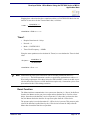
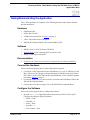
The advantage of a conventional power supply method over the parasite power method is
that an external MOSFET pull-up is not required. As a result, the 1-Wire bus is free from
transaction overhead associated with the use of parasite power. Figure 1 shows a schematic diagram of the 1-Wire bus with an external pull-up resistor that is used to pull the
data line to logic High using an external power supply.
Figure 1. Schematic Diagram of the 1-Wire Interface with a Z8F1680 Series MCU
Discussion: 1-Wire Bus Operation
The 1-Wire bus consists of four basic operations: Reset, Write 0 Bit, Write 1 Bit and Read
Bit. This section discusses these four operations wherein the activity of the 1-Wire protocol occurs.
AN033101-0412
Page 2 of 13
Develop a Dallas 1-Wire Master Using the Z8F1680 Series of MCUs
Application Note
Reset
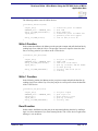
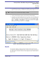
The following events occur when a Reset command is issued over the 1-Wire bus; see Figure 2.
•
The pull-up resistor pulls the data line High at all times.
•
The 1-Wire Master initiates the data line Low for at least 480 µs and not more than
640 µs during its reset sequence, then sets the data line to open drain or high impedance.
•
The 1-Wire Slave sets a presence pulse by triggering the data line to Low after 15–60 µs
from the time the Master sets the data line to open drain.
•
The Master checks the data line for this presence pulse approximately 60–240 µs from
the time the data line is set to open drain.
•
The 1-Wire Slave undergoes a recovery period of at least 1 µs.
Figure 2. Reset Timing Diagram
Write 0
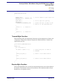
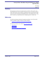
The following sequence of events occurs when a Write0 command is issued over the 1Wire bus; see Figure 3.
1. The Master writes to bit 0 by pulling the data line Low for at least 60 µs, then releasing
the data line as open drain.
2. The Master waits for a minimum recovery period of 1 µs before sending the next bit.
Write 1
The following sequence of events occurs when a Write1 command is issued over the 1Wire bus; see Figure 3.
AN033101-0412
Page 3 of 13
Develop a Dallas 1-Wire Master Using the Z8F1680 Series of MCUs
Application Note
1. The Master writes to bit 1 by pulling the data line Low within 15 µs, then releasing it
by setting the data line to open drain.
2. The Master waits for a minimum recovery period of 1 µs before sending the next bit.
Figure 3. Write Timing Diagram
Read
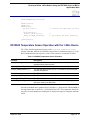
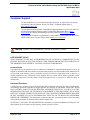
The following sequence of events occurs when a Read command is issued over the 1-Wire
bus:
1. The Master pulls the data line Low for at least 1 µs, then releases the bus.
2. After releasing the data line, the Master waits for a period of 15 µs, then checks the
data line.
3. The Master reads logic 0 if the data line is Low within 15 µs; otherwise, the Master
reads logic 1 if the data line is High.
A read/write timing diagram of these events is shown in Figure 4.
AN033101-0412
Page 4 of 13
Develop a Dallas 1-Wire Master Using the Z8F1680 Series of MCUs
Application Note
Figure 4. Read Timing Diagram
Software Implementation
1-Wire communication consists of a three-phase operation sequence that includes a Reset
sequence, a ROM sequence and a function sequence. The Write 0, Write 1, and Read bits
are the basic building blocks of the ROM and function command sequences. All timing
requirements for the Maxim/Dallas 1-Wire bus are catered by the Z8F1680 MCU’s timers
via interrupts. An API library has been created with the 1-Wire function; this library can
be modified by the user depending on the GPIO pin to be used with the 1-Wire interface.
There are items to consider regarding the usage of Timer0 and Timer1 to meet the timing
requirement range imposed by the Maxim/Dallas 1-Wire protocol, as the following discussion shows.
Timer0
•
Required time interval: 1 ms
•
Prescale = 4
•
Mode = CONTINUOUS
•
Timer Clock Frequency = 20 MHz
The equation below calculates the required CONTINUOUS Mode time-out interval.
CONTINUOUS_Mode_Time-Out_Period(s) =
AN033101-0412
reloadValue * prescale
TimerClockFrequency ( Hz)
Page 5 of 13
Develop a Dallas 1-Wire Master Using the Z8F1680 Series of MCUs
Application Note
Plugging these values into the above equation to achieve a CONTINUOUS Mode time-out
interval of 1 ms solves for the Timer0 reload value, as follows:
1 msec =
reloadValue * 4
20,000,000 Hz
reloadValue = 5000 or 0x1388
Timer1
•
Required time interval: 10.4 µs
•
Prescale = 4
•
Mode = CONTINUOUS
•
Timer Clock Frequency = 20 MHz
Using the same equation used to calculate for Timer0, we can calculate the Timer1 reload
value:
10.4 µsec =
reloadValue * 4
20,000,000 Hz
reloadValue = 52 or 0x34
Note: Additional delay time can be factored in with an assembly instruction called NOP
asm("nop"). The NOP instruction is used as a special delay mechanism to achieve a 1Wire timing requirement of less than 10.4 µs; the Z8F1680 MCU’s timer is not able to provide this delay time. However, a NOP instruction requires only 1 instruction cycle to complete and meets this 1-Wire timing restriction.
Reset Function
The Master initiates communication via a system reset function (i.e., Reset). In this Reset
function, the Master sets the port pin to output and sets the data line to Low for at least
480 µs, then releases the data line, sets it to input and, 15–60 µs after it releases the data
line, the Master checks the data line for a presence pulse from the 1-Wire device.
The presence pulse is used to determine if a 1-Wire device is present. This presence pulse
exists if the data line is pulled down by the 1-Wire device between 60-240 µs after the
Master has released the data line as open drain.
AN033101-0412
Page 6 of 13
Develop a Dallas 1-Wire Master Using the Z8F1680 Series of MCUs
Application Note
The following routine resets all 1-Wire devices.
void Reset_Function(void)
{
output_TX();
ONEWIRE_OUT = ~ONEWIRE_PIN;
delay_us(TIME_480to640 µs);
input_RX();
delay_us(TIME_470 µs);
//
//
//
//
//
//
initialize ports as
Pull LOW
delay 480µs Rx
initialize ports as
presence pulse will
rest of 480 µs slot
OUTPUT
INPUT and
appear
Tx
}
Write 0 Function
In the routine that follows, the Master sets the port pin to output and pulls the data line by
sending logic Low within 60-120 µs. The port pin is next set to input to release the data
line; a recovery period of 1 µs ensues on the 1-Wire device.
void Write_Zero_Bit(void)
{
output_TX();
ONEWIRE_OUT = ~ONEWIRE_PIN;
delay_us(TIME_60to120 µs);
input_RX();
delay_us(TIME_RECOVERY);
//
//
//
//
//
//
//
set port to OUTPUT
LOGIC LOW
time slot at 60-120 µs
pull up (release) SET AS INPUT
to draw pull-up
recovery time from 1 µs to
infinity
}
Write 1 Function
In the following routine, the Master sets the port pin to output and pulls the data line by
sending a logic Low within 15 µs. Next, the port pin is set to input to release the data line
of the 1-Wire device.
void Write_One_Bit(void)
{
output_TX();
ONEWIRE_OUT = ~ONEWIRE_PIN;
asm("nop");
input_RX();
delay_us(TIME_RECOVERY);
}
//
//
//
//
//
set port output
pull logic low
delay within 1-15 µs
pull up (release)
recovery time
Read Function
In this routine, the Master sets the port pin to output and pulls the data line by sending a
logic Low for a minimum of 1 µs, then releasing the bus. The 1-Wire device begins transmitting a 1 or 0 on the bus.
AN033101-0412
Page 7 of 13
Develop a Dallas 1-Wire Master Using the Z8F1680 Series of MCUs
Application Note
UINT8 Read_Bit(void)
{
output_TX();
ONEWIRE_OUT &= ~ONEWIRE_PIN;
asm("nop");
input_RX();
asm("nop");
if(ONEWIRE_IN&ONEWIRE_PIN)
// set as output to pull logic Low
// set as input for pull-up
// checks the bits of data if the
// data is in the specified bus
{
return 1;
}
else
{
return 0;
}
// reads as 1
// reads as 0
}
Transmit Byte Function
In the following routine, the transmit byte function is used to transmit a byte of data to the
1-Wire device. These 8 bits of data are interpreted as Write0 and Write1, with the least
significant bit sent first.
void onewire_CMD(UINT8 data)
{
UINT8 i=0;
for (i=0;i<8;i++)
{
if (data & (0x01 << i))
// check every bit to send to
// DS18S20
{
Write_One_Bit();
}
else
{
Write_Zero_Bit();
}
// write 1 into 1-Wire device
// write 0 into 1-Wire device
}
}
Receive Byte Function
In the routine that follows, the received byte function interprets the received bits of data on
the data line. This function is also used as an indicator of the maximum number of bytes
that the device is expected to receive.
AN033101-0412
Page 8 of 13
Develop a Dallas 1-Wire Master Using the Z8F1680 Series of MCUs
Application Note
UINT8 ONEWIRE_Receive(void)
{
UINT8 value=0;
UINT8 i=0;
UINT8 bit=0;
for(i=0;i<8;i++)
{
bit=read_bit();
if(bit) value|=(1<<i);
delay_us(TIME_50to60 µs);
}
return(value);
}
// receives the data byte (8 bits)
//
// 50 µs delay for data integrity
DS18S20 Temperature Sensor Operation with the 1-Wire Device
The 1-Wire interface application focuses on the void Read_Temperature(void)
function. With this function, the DS18S20 sensor follows a transaction sequence (i.e., the
Reset, ROM and Function sequences) of the 1-Wire interface, as indicated in Table 1.
Table 1. DS18S20 Temperature Sensor Functions
Function
Description
Reset_Function();
The Z8F1680 MCU issues reset pulse and check if DS18S20
responds with a presence pulse.
onewire_CMD(SKIP_ROM);
The Z8F1680 MCU issues Skip ROM command to DS18S20.
onewire_CMD(CONVERT_T);
The Z8F1680 MCU issues Convert T command in which DS18S20
converts temperature.
Reset_Function();
The Z8F1680 MCU issues reset pulse.
onewire_CMD(SKIP_ROM);
The Z8F1680 MCU issues Skip ROM Command.
onewire_CMD(RD_SCRPAD);
The Z8F1680 MCU issues Read Scratchpad to DS18S20.
ONEWIRE_Receive();
The Z8F1680 MCU reads entire scratchpad including the generated
CRC byte made by the DS18S20.
After the scratchpad data is gathered, Byte 0 and Byte 1 – which are the LSB and MSB of
the temperature data, respectively – are fetched by the CPU. This temperature data is factored into an actual temperature reading that is displayed in degrees Centigrade and Fahrenheit.
AN033101-0412
Page 9 of 13
Develop a Dallas 1-Wire Master Using the Z8F1680 Series of MCUs
Application Note
Testing/Demonstrating the Application
This 1-Wire application is comprised of the following hardware and software elements,
plus documentation.
Hardware
•
USB Smart Cable
•
USB to RS-232 cable
•
4.7 KΩ resistor (labeled R1 in Figure 1 on page 2)
•
1-Wire Temperature Sensor (DS18S20)
•
Z8F1680 Development Board with external 20 MHz crystal
Software
•
ZDS II version 5.0.0 for Z8 Encore! XP MCUs
•
AN0331-SC01 zip file containing project and source files
•
BAUD_57600 HyperTerminal file
Documentation
•
Z8 Encore! XP F1680 Series (28-Pin) Development Kit User Manual (UM0203)
Connect the Hardware
Observe the following procedure to connect all hardware elements.
1. Connect the 1-Wire Temperature Sensor (DS18S20) to VCC (pin 3), GND (pin 5) and
DQ (1-Wire bus). The DQ pin is connected through a 4.7 KΩ pull-up resistor to Port C
Pin 7 (Pin 13 of JP2) of the Z8F1680 Development Board; see the schematic diagram
presented in Figure 1 on page 2.
2. Connect the USB to RS-232 cable to the PC, and connect the USB Smart Cable to the
Z8F1680 Development Board.
3. Connect the power cable to apply power to the Z8F1680 Development Board.
Configure the Software
Observe the following procedure to configure the software.
1. Open the BAUD_57600 HyperTerminal file located in the AN0331-SC01.zip file.
Configure the settings in HyperTerminal to:
– Baud = 57600
– Data Bits = 8
– Parity = None
– Stop Bits = 1
– Flow Control = None
AN033101-0412
Page 10 of 13
Develop a Dallas 1-Wire Master Using the Z8F1680 Series of MCUs
Application Note
2. Open ZDS II, then navigate via the File menu in ZDS II to open the project file labeled
AN0331 - Develop 1-Wire interface using Z8F1680.zdsproj.
Note: The project is set to an external clock frequency of 20 MHz.
3. Compile and download the program to the Z8F1680 Development Board.
4. You should see the HyperTerminal display shown in Figure 5; the Serial ID may vary
depending on the type of 1-Wire device you are using. If you do not see this display,
verify your Configure Target settings in the ZDS II project settings (Project → Settings... → Debugger → Setup button) to ensure that Clock Source is set to External and that Clock Frequency (MHz) is set to 20.00000.
Figure 5. 1-Wire Interface Output to HyperTerminal
Results
The temperature readings, as displayed in HyperTerminal, indicate that the firmware
developed for the Z8F1680 and DS18S20 devices satisfies the the timing requirements of
the 1 Wire interface. The Device ID of the 1-Wire temperature sensor is detected and displayed as well.
AN033101-0412
Page 11 of 13
Develop a Dallas 1-Wire Master Using the Z8F1680 Series of MCUs
Application Note
Summary
This application note discusses the implementation of a Dallas 1-Wire interface using
Zilog’s Z8F1680 Series microcontrollers. The application passes the timing requirements
of the 1-Wire interface, and successfully implements the 1-Wire interface with a 1-Wire
temperature sensor. The firmware described herein can be used with other types of 1-Wire
devices, which can be determined by means of identifying a device’s family code.
References
The following document describes the functional specifications of the Z8F1680 MCU,
which is a member of Zilog’s Z8 Encore! XP Series of MCUs.
•
Z8 Encore! XP F1680 Series Product Specification (PS0250)
The following documents can be found on http://www.maxim-ic.com.
•
1-Wire Devices
•
1-Wire Tutorial
•
1-Wire Parasite-Power Digital Thermometer
AN033101-0412
Page 12 of 13
Develop a Dallas 1-Wire Master Using the Z8F1680 Series of MCUs
Application Note
Customer Support
To share comments, get your technical questions answered, or report issues you may be
experiencing with our products, please visit Zilog’s Technical Support page at
http://support.zilog.com.
To learn more about this product, find additional documentation, or to discover other facets about Zilog product offerings, please visit the Zilog Knowledge Base at http://
zilog.com/kb or consider participating in the Zilog Forum at http://zilog.com/forum.
This publication is subject to replacement by a later edition. To determine whether a later
edition exists, please visit the Zilog website at http://www.zilog.com.
Warning: DO NOT USE THIS PRODUCT IN LIFE SUPPORT SYSTEMS.
LIFE SUPPORT POLICY
ZILOG’S PRODUCTS ARE NOT AUTHORIZED FOR USE AS CRITICAL COMPONENTS IN LIFE
SUPPORT DEVICES OR SYSTEMS WITHOUT THE EXPRESS PRIOR WRITTEN APPROVAL OF
THE PRESIDENT AND GENERAL COUNSEL OF ZILOG CORPORATION.
As used herein
Life support devices or systems are devices which (a) are intended for surgical implant into the body, or (b)
support or sustain life and whose failure to perform when properly used in accordance with instructions for
use provided in the labeling can be reasonably expected to result in a significant injury to the user. A
critical component is any component in a life support device or system whose failure to perform can be
reasonably expected to cause the failure of the life support device or system or to affect its safety or
effectiveness.
Document Disclaimer
©2012 Zilog, Inc. All rights reserved. Information in this publication concerning the devices, applications,
or technology described is intended to suggest possible uses and may be superseded. ZILOG, INC. DOES
NOT ASSUME LIABILITY FOR OR PROVIDE A REPRESENTATION OF ACCURACY OF THE
INFORMATION, DEVICES, OR TECHNOLOGY DESCRIBED IN THIS DOCUMENT. ZILOG ALSO
DOES NOT ASSUME LIABILITY FOR INTELLECTUAL PROPERTY INFRINGEMENT RELATED
IN ANY MANNER TO USE OF INFORMATION, DEVICES, OR TECHNOLOGY DESCRIBED
HEREIN OR OTHERWISE. The information contained within this document has been verified according
to the general principles of electrical and mechanical engineering.
Z8, Z8 Encore!, Z8 Encore! XP and ZMOTION are trademarks or registered trademarks of Zilog, Inc. All
other product or service names are the property of their respective owners.
AN033101-0412
Page 13 of 13