1
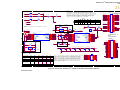
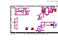
Z8F083A0128ZCOG
Z8 Encore!® F083A Series
Development Kit
User Manual
UM020604-0508
Copyright ©2008 by Zilog®, Inc. All rights reserved.
www.zilog.com
Z8 Encore!® F083A Series Development Kit
User Manual
ii
Revision History
Each instance in Revision History reflects a change to this document from
its previous revision. For more details, refer to the corresponding pages
and appropriate links in the table below.
Date
Revision
Level
Description
Page
No
May 2008
04
Updated Introduction section.
1
March
2008
03
Modified Table 2 in Schematics to
incorporate changes to R15 from 220
Ohm to 0 Ohm. Added Note 3 to the
Schematics.
8, 9
December 02
2007
Updated Zilog logo, Zilog text, Disclaimer All
section, and implemented style guide.
Removed XP from Z8 Encore! XP F0830/
F083A.
July 2006
Original issue.
UM020604-0508
01
All
Revision History
Z8 Encore!® F083A Series Development Kit
User Manual
iii
Table of Contents
Introduction . . . . . . . . . . . . . . . . . . . . . . . . . . . . . . . . . . . . . . . . . . . . . 1
Kit Contents . . . . . . . . . . . . . . . . . . . . . . . . . . . . . . . . . . . . . . . . . . . 2
Installation . . . . . . . . . . . . . . . . . . . . . . . . . . . . . . . . . . . . . . . . . . . . . . 3
Z8 Encore!® F083A Series Development Board . . . . . . . . . . . . . . . .
Introduction . . . . . . . . . . . . . . . . . . . . . . . . . . . . . . . . . . . . . . . . . . .
Features . . . . . . . . . . . . . . . . . . . . . . . . . . . . . . . . . . . . . . . . . . . . . .
MCU . . . . . . . . . . . . . . . . . . . . . . . . . . . . . . . . . . . . . . . . . . . . . . . . .
Jumper Settings . . . . . . . . . . . . . . . . . . . . . . . . . . . . . . . . . . . . . . . .
External Interface Headers JP1 and JP2 . . . . . . . . . . . . . . . . . . . . .
4
4
5
6
6
6
Schematic . . . . . . . . . . . . . . . . . . . . . . . . . . . . . . . . . . . . . . . . . . . . . . 7
Customer Support. . . . . . . . . . . . . . . . . . . . . . . . . . . . . . . . . . . . . . . 10
UM020604-0508
Table of Contents
Z8 Encore!® F083A Series Development Kit
User Manual
1
Introduction
Zilog’s Z8 Encore!® F083A Series MCU is part of the line of Zilog®
microcontroller products. The Z8 Encore! F083A Series MCU Development Kit (Z8F083A0128ZCOG) enables you to become familiar with the
hardware and software tools available with this product. This kit consists
of the 8 KB version of the Z8 Encore! development board that supports
and presents the features of the Z8 Encore! F083A Series. This kit allows
you to write application software and contains all the supporting documents.
The Z8 Encore! F083A Series devices support up to 8 KB Flash Program
Memory and 256 B register RAM that is pin-for-pin compatible with the
award-winning Z8 Encore! XP F0822 Series Flash Microcontrollers
family.
The Z8 Encore! F083A Series device features up to eight channels of fast
analog-to-digital conversion (2.15 µs). The ADC on the Z8 Encore!
F083A is one of the fastest 10-bit ADCs available in a 28-pin or smaller
package. The Z8 Encore! F083A is built for speed to handle rigorous
application requirements for motor control, sensor interfacing, ballast
control, and appliance controls. The single-pin debugger and programming interface simplifies code development and allows easy in-circuit
programming.
This user manual acquaints you with the Z8 Encore! F083A Series MCU
Development Kit, and gives instructions on setting up and using the tools
to start building designs and applications. Z8F083ASJ020 is the silicon
used in the board. For more information, refer to Z8 Encore!® F083A
Series Product Specification (PS0263).
UM020604-0508
Introduction
Z8 Encore!® F083A Series Development Kit
User Manual
2
Kit Contents
For information on kit contents, refer to Z8 Encore! XP®/Z8 Encore!®
(F0822, F082A, F1680, and F083A Series) Development Kits Quick Start
Guide (QS0043).
UM020604-0508
Introduction
Z8 Encore!® F083A Series Development Kit
User Manual
3
Installation
For software installation and setup of the Z8 Encore!® F083A Series
Development Kit, refer to Z8 Encore! XP®/Z8 Encore!® (F0822, F082A,
F1680, and F083A Series) Development Kits Quick Start Guide
(QS0043).
UM020604-0508
Installation
Z8 Encore!® F083A Series Development Kit
User Manual
4
Z8 Encore!® F083A Series
Development Board
Introduction
The Z8 Encore!® F083A Series Development Board is a development and
prototyping board for the Z8 Encore! F083A Series MCU. The board provides a tool to evaluate features of Z8 Encore! F083A Series MCU, and to
start developing an application before building the hardware.
Figure 1. Z8 Encore!® F083A Series Development Board
(see Schematic on page 7 for details on components not installed on this board)
UM020604-0508
Z8 Encore!® F083A Series
Z8 Encore!® F083A Series Development Kit
User Manual
5
Features
The key features of Z8 Encore! F083A Series include:
•
•
•
•
•
•
•
•
20 MHz eZ8 CPU
•
•
•
•
•
•
•
•
•
•
•
Watchdog Timer (WDT) with dedicated internal RC oscillator
UM020604-0508
Up to 8 KB Flash memory with in-circuit programming capability
Up to 256 B register RAM
100 B non-volatile data storage (NVDS)
Up to 23 I/O pins depending upon package
Internal precision oscillator (IPO)
External crystal oscillator
Two enhanced 16-bit timers with capture, compare, and PWM capability
Single-pin, On-Chip Debugger (OCD)
Fast 8-channel, 10-bit analog-to-digital converter (ADC)
On-chip analog comparator
Up to 18 vectored interrupts
Voltage Brownout (VBO) protection
Power-On Reset (POR)
2.7 V to 3.6 V operating voltage
Up to thirteen 5 V tolerant input pins
20- and 28-pin packages
0 °C to +70 °C standard temperature range and -40 °C to +105 °C
extended temperature operating ranges
Z8 Encore!® F083A Series
Z8 Encore!® F083A Series Development Kit
User Manual
6
MCU
The Z8 Encore! F083A Series MCU is member of a family of Zilog®
microcontroller products based upon the 8-bit eZ8 core CPU. The Flash
in-circuit programming capability allows for faster development time and
program changes in the field. The eZ8 core CPU is upward compatible
with existing Z8® instructions. The successive approximation register
(SAR) ADC on the Z8 Encore! F083A is one of the fastest 10-bit ADCs
available in a 28-pin or smaller package. The Z8 Encore! F083A is built
for speed to handle rigorous application requirements for motor control,
sensor interfacing, ballast control, and appliance controls.
The development board contains circuitry to support and present all the
features of the Z8 Encore! F083A Series. For more information on the
Z8 Encore!® family of devices, refer to Z8 Encore!® F083A Series
Product Specification (PS0263) available for download at
www.zilog.com.
Jumper Settings
The only jumper available on the Z8 Encore! F083A development board
is JP5, which affects U5 RESET/PD0. Set JP5 as follows:
•
•
JP5 OUT (default): PD0 (GPIO)
JP5 IN: RESET when SW1 pressed
External Interface Headers JP1 and JP2
Figure 2 on page 8 displays the external interface headers JP1 and JP2.
UM020604-0508
Z8 Encore!® F083A Series
Z8 Encore!® F083A Series Development Kit
User Manual
7
Schematic
This section includes schematics for the Z8 Encore!® F083A Series
Development Board (see Figure 2 and Figure 3 on page 9).
The following components appear in the schematic but are not installed
on the board:
•
•
•
•
•
UM020604-0508
C1, C2, C5, C6, C9, C11 through C18
JP3, JP4
P1
R2 through R5
U1, U3, U4
Schematic
Z8 Encore!® F083A Series Development Kit
User Manual
8
5
4
D2
PA6_nT1OUT
1
2
100
GREEN
R8
D3
PA7_T1OUT
1
R9
SW2
VCC_33V
2
GND
100
YELL
TEST
100K
D
1
R13 R16
R17
R22
OUT
IN
OUT
IN
IN
OUT
OUT
Analog
Supply
IN
OUT
IN
OUT
OUT
optional
IN
PA2
GND
GND
R12
GPIO
10
RED
1
If Module is plugged onto the Dev Platform the local
RS232 interface is disabled by pin 50 of JP2
JP2
U8
C21...C23
PA3_CTS0
PA4_RXD0
GND
NOTE 1:
R12
SW1
0
U8
1
IO
2
PA0_T0IN_JP
PA1_T0OUT_JP
0
R21
0
1
2
3
4
5
6
7
8
9
10
JP5
PB6
3
R22
PB1/ANA1
PB2/ANA2
PB3/CLKIN/ANA3
VDD
PA0/T0IN/T0OUT/XIN/
PA1/T0OUT/XOUT
GND
PA2/DE
PA3/CTS0
PA4/RXD0
PB0_ANA0
PC3_COUT
PC2_ANA6
PC1_ANA5
PC0_ANA4
DBG
PD0
PA7_T1OUT
PA6_nT1OUT
PA5_TXD0
20
19
18
17
16
15
14
13
12
11
C22
VCC_33V
PA0_T0IN
PA1_T0OUT
GND
0.033uF C21 C10
30uF
0.033uF 0.001uF
PA2
PA3_CTS0
PA4_RXD0
PA5_TXD0
PA3_CTS0
PA4_RXD0
PA5_TXD0
Z8F04xA
R14
0
0
PB5_JP
PB2_ANA2
PB4_ANA7
PB5
PB3_ANA3
SENSE
C23
+
1
2
0
U5
PB0/ANA0
PC3/COUT/LED
PC2/ANA6/LED
PC1ANA5/CINN/LED
PC0/ANA4/CINP/LED
DBG
RESET/PD0
PA7/T1OUT
PA6/T1IN/T1OUT
PA5/TXD0
-RESET
VCC_33V
VCC_33V
HEADER 2
EMI Filter
20 pin footprint
U6
PB1_ANA1
PB2_ANA2
PB3_ANA3
VCC_33V
PA0_T0IN
PA1_T0OUT
GND
PA2
PA3_CTS0
PA4_RXD0
IO
1
2
3
4
5
6
7
8
9
10
11
12
13
14
R16 0
PB2/ANA2
PB4/ANA7
PB5/Vref
PB3/ANA3/CLKIN
PB6(AVDD)
VDD
PA0/T0IN/T0OUTXIN
PA1/T0OUT/XOUT
GND
PB7(AGND)
PA2/DE
PA3/CTS0
PA4/RXD0
PA5/TXD0
PB1/ANA1
PB0/ANA0
PC3/COUT/LED
PC2/ANA6/LED
PC1/ANA5/CINN/LED
PC0/ANA4/CINP/LED
DBG
RESET/PD0
PC7/LED
PC6/LED
PA7/T1OUT
PC5/LED
PC4/LED
PA6/T1IN/T1OUT
1
3
5
7
9
11
13
15
17
19
21
23
25
27
29
31
33
35
A21
37
A22
39
-CS0
41
-CS2
43
D1
45
D3
47
D5
49
D7
51
-MREQ 53
GND
55
-WR
57
-BUSACK 59
1
3
3
PB7
PB0_ANA0
2
2
1
PB1_ANA1
PB2_ANA2
PB3_ANA3
PC0_ANA4
PC1_ANA5
PC2_ANA6
PB4_ANA7
C20
C11
0.001uF
20 MHz
C12
0.001uF
C13
0.001uF
C14
0.001uF
C15
0.001uF
C16
0.001uF
C17
0.001uF
C18
0.001uF
NOTE 2
GND
J2
TABLE 2
Clock Mode
Internal Only
A
R14
R15
none
none
Crystal
0 Ohm
0 Ohm
Ceramic Res
0 Ohm
0 Ohm
External CMOS
none
none
R18
none
C19
none
none
Yes
none
none
none
none
C20
Note 2: The XP supports internal, external crystal, external
ceramic resonator, external R/C and external CMOS drive
clock modes. R14, R15, R18, C19, C20 and Y1 are used to
support the clock mode selected. The development board is
shipped configured for external 20MHz ceramic resonator or
internal clock operation. When using Internal oscilator,
pins 7 and 8 could be used as GPIO ports PA0 and PA1. To do
so install R20 and R21.
Table 2 shows the recommended clock mode configurations.
Y1
none
none
Yes
Yes
none
Yes
none
none
PB0_ANA0
PB1_ANA1
PB2_ANA2
PB3_ANA3
PC0_ANA4
PC1_ANA5
PC2_ANA6
PB4_ANA7
1
3
5
7
9
11
13
15
2
4
6
8
10
12
14
16
PA5_TXD0
GND
-DIS_232
-DIS_IRDA
-DIS_IrDA
GND
VCC_33V
A0
A3
VCC_33V
A7
A9
A14
A16
GND
A1
A12
A20
A17
-DIS_FLASH
VCC_33V
A23
-CS1
D0
D2
D4
GND
D6
-IOREQ
-RD
-INSTRD
-BUSREQ
B
HEADER 30x2/SM
A
HEADER 8X2
Title
(Use PA0_T0IN
pin on JP2)
XP 4K MDS Processor Module. Schematic.
Size
B
Date:
5
4
3
2
Figure 2. Schematic, Z8 Encore!® F083A Series MCU Development Board
UM020604-0508
PD0
GND
2
4
6
8
10
12
14
16
18
20
22
24
26
28
30
32
34
36
38
40
42
44
46
48
50
52
54
56
58
60
-TRSTN
-F91_WE
GND
A6
A10
GND
A8
A13
A15
A18
A19
A2
A11
A4
A5
NOTE 1:
C19
D
connector 1
for
reference
onlyJP1
DBG
1M
Y1
PC0_ANA4
PB2_ANA2
PB0_ANA0
GND
PC5
PC6
PB5_JP
PA0_T0IN_JP
PA1_T0OUT_JP
PA2
HEADER 30x2/SM
R18
B
2
4
6
8
10
12
14
16
18
20
22
24
26
28
30
32
34
36
38
40
42
44
46
48
50
52
54
56
58
60
C
PB1_ANA1
PB0_ANA0
PC3_COUT
PC2_ANA6
PC1_ANA5
PC0_ANA4
DBG
PD0
PC7
PC6
PA7_T1OUT
PC5
PC4
PA6_nT1OUT
28
27
26
25
24
23
22
21
20
19
18
17
16
15
R17 0
GND
connector
2
PC2_ANA6
1
3
5
7
9
11
13
15
17
19
21
23
25
27
29
31
33
35
37
39
41
43
45
47
49
51
53
55
57
59
28 pin footprint
Z8F04xA_28
R15
0
PB6
PB7
RESET/TEST2
R13
GND
VCC_33V
R20
R19 10K
GND
NOTE 3:
Resistors R20 and R21 are not populated. See Note 2.
C
PB4_ANA7
PC1_ANA5
PB3_ANA3
PB1_ANA1
VCC_33V
PC4
PC7
PC3_COUT
PA6_nT1OUT
GND
PA7_T1OUT
TABLE 1
100
2
VCC_33V
VCC_33V
2
R11
R10
D4
PC3_COUT
3
Note 1:
PB6 and PB7 are dual function pins (GPIO or Analog supply)
R12, R13, R16, and R17 are zero-ohm resistors used in
conjunction with GPIO Control Registers to select function
desired. C21, C22, and C23 are bypass capacitors that are used
for better noise rejection. U8 is an optional filter that can
be used to improve the quality of the Analog Supply. The
development board is shipped configured for Analog Supply.
Table 1 shows the configurations recommended
R7
Document Number
Rev
96C0941-001
Tuesday, March 18, 2008
D
Sheet
1
2
of
3
Z8 Encore!® F083A Series Development Kit
User Manual
9
5
4
3
2
1
VCC_33V
J1
PWR JACK
VCC
RXE050
+ C3
C4
0.1uF
R23
10K
100/10
-Z_RST
5
VIN
OUT
2
4
SENSE
SHDN
GND
SENSE
LT1129-3.3/DD
VCC_33V
1
VCC_33V
PA5_TXD0
C1+
4
C1-
5
C2+
C6
0.1uF
6
C2-
PA5_TXD0
U7
3
D
2
C1
0.1uF
19
VCC
5V
U1
C2
0.1uF
F1
V+
3
C5
0.1uF
7
13
T1IN
T1OUT
17
GND
12
T2IN
T2OUT
8
PA3_CTS0
15
R1OUT
PA4_RXD0
10
R1
CONSOLE
GND
P1
V-
TXD0
CTS0
RXD0
1
6
2
7
3
8
4
9
5
D
+ C7
C8
680
PA3_CTS0
100/10
PA4_RXD0
2
0.1uF
R24
15K
R2OUT
R1IN
16
R2IN
9
DB9 Female
USER
D1
LED
1
3.3 OK
EN
SHDN
NC
NC
14
11
MAX3222
GND
18
1
20
GND
2
3
1
VCC_33V
GND
R2
10K
C
U3A
14
C
14
74LVC04/SO
U3B
1
-DIS_232
2
7
74LVC04/SO
3
JP3
4
1
2
7
GND
U3C
74LVC04/SO
GND
5
R3
C9
VCC_33V
6
68
330nF
R4
7
B
14
U3D
PA5_TXD0
74LVC04/SO
9
-DIS_IRDA
10
IRDA_SD
8
PA4_RXD0
7
VCC
1
LEDA
2
TXD
4
SD
3
RXD
6
GND
7
JP4
5
1
2
0
14
R5
10K
U3E
74LVC04/SO
11
B
U4
2R7
T
14
DIS RS232
GND
ZHX1810
14
DIS IRDA
GND
U3F
VCC_33V
R6
10K
7
A
12
1
2
3
4
5
13
1
2
3
4
5
74LVC04/SO
TP1
GND
TP2
P2
VCC_33V
GND
1
3
5
DBG
INTERFACE
2
4
6
A
-Z_RST
DBG
DBG
Title
XP 4K MDS Processor Module. Schematic.
Header 3x2
Size
B
Date:
5
4
3
2
Figure 3. Schematic, Z8 Encore!® F083A Series MCU Development Board
UM020604-0508
Document Number
Rev
96C0941-001
Wednesday, March 12, 2008
D
Sheet
1
3
of
3
Z8 Encore!® F083A Series Development Kit
User Manual
10
Customer Support
For answers to technical questions about the product, documentation, or
any other issues with Zilog’s offerings, please visit Zilog’s Knowledge
Base at http://www.zilog.com/kb.
For any comments, detail technical questions, or reporting problems,
please visit Zilog’s Technical Support at http://support.zilog.com.
UM020604-0508
Customer Support
Z8 Encore!® F083A Series Development Kit
User Manual
11
Warning: DO NOT USE IN LIFE SUPPORT
LIFE SUPPORT POLICY
Z IL O G ' S P RO D U C T S A RE N O T A U T H O R IZ E D F O R U SE A S CR IT ICA L
COMPONENTS IN LIFE SUPPORT DEVICES OR SYSTEMS WITHOUT THE
EXPRESS PRIOR WRITTEN APPROVAL OF THE PRESIDENT AND GENERAL
COUNSEL OF ZILOG CORPORATION.
As used herein
Life support devices or systems are devices which (a) are intended for surgical implant
into the body, or (b) support or sustain life and whose failure to perform when properly
used in accordance with instructions for use provided in the labeling can be reasonably
expected to result in a significant injury to the user. A critical component is any
component in a life support device or system whose failure to perform can be reasonably
expected to cause the failure of the life support device or system or to affect its safety or
effectiveness.
Document Disclaimer
©2008 by Zilog, Inc. All rights reserved. Information in this publication concerning the
devices, applications, or technology described is intended to suggest possible uses and
may be superseded. ZILOG, INC. DOES NOT ASSUME LIABILITY FOR OR
PROVIDE A REPRESENTATION OF ACCURACY OF THE INFORMATION,
DEVICES, OR TECHNOLOGY DESCRIBED IN THIS DOCUMENT. ZILOG ALSO
D O E S N O T A S S U M E L I A B I L I T Y F O R I N T E L L E C T U A L P R O P E RT Y
INFRINGEMENT RELATED IN ANY MANNER TO USE OF INFORMATION,
DEVICES, OR TECHNOLOGY DESCRIBED HEREIN OR OTHERWISE. The
information contained within this document has been verified according to the general
principles of electrical and mechanical engineering.
Z8 Encore! and Z8 Encore! XP are registered trademarks of Zilog, Inc. All other product
or service names are the property of their respective owners.
UM020604-0508
Mouser Electronics
Related Product Links
692-Z8F083A0128ZCOG - ZiLOG Z8F083A0128ZCOG