1
Modicon 984
Programmable
Controller
Systems Manual
GM--0984--SYS Rev. B
May, 1991
MODICON, Inc., Industrial Automation Systems
One High Street
North Andover, Massachusetts 01845
DOK-
1
2
DOK-
Table of Contents
Chapter 1 The 984 Programmable Controllers . . . . . . . . . . 1
Modicon’s Family of Programmable Controllers . . . . . . . . . . . . . . . . . . . . . . . 2
The 984 Family
............................................... 2
Controller Compatibility . . . . . . . . . . . . . . . . . . . . . . . . . . . . . . . . . . . . . . . . . . 3
984 Controller Performance and Capacity Characteristics . . . . . . . . . . . . . . 4
How a 984 System Provides Application Control . . . . . . . . . . . . . . . . . . . . . . . 6
The 984 Control Architecture: An Overview . . . . . . . . . . . . . . . . . . . . . . . . . 6
Reliability and Maintainability . . . . . . . . . . . . . . . . . . . . . . . . . . . . . . . . . . . . . 7
P190-Style Panel Software Support . . . . . . . . . . . . . . . . . . . . . . . . . . . . . . . . . 8
Standard Panel Software Editors . . . . . . . . . . . . . . . . . . . . . . . . . . . . . . . . . . 8
Special Loadable Software . . . . . . . . . . . . . . . . . . . . . . . . . . . . . . . . . . . . . . . 9
MODSOFT Panel Software Support . . . . . . . . . . . . . . . . . . . . . . . . . . . . . . . . 10
Sequential Function Charts . . . . . . . . . . . . . . . . . . . . . . . . . . . . . . . . . . . . . . 10
MODSOFT Macros . . . . . . . . . . . . . . . . . . . . . . . . . . . . . . . . . . . . . . . . . . . . . 11
MODSOFT Operating Modes . . . . . . . . . . . . . . . . . . . . . . . . . . . . . . . . . . . . 11
Overview of the 984 Instruction Set . . . . . . . . . . . . . . . . . . . . . . . . . . . . . . . . . 12
Chapter 2 Optional and Peripheral Control Devices . . . 15
Programming Panels . . . . . . . . . . . . . . . . . . . . . . . . . . . . . . . . . . . . . . . . . . . . .
The P230
..............................................
The P190 Panels . . . . . . . . . . . . . . . . . . . . . . . . . . . . . . . . . . . . . . . . . . . . . .
Using Industry-standard PCs as Programming Panels . . . . . . . . . . . . . . .
The P965 Data Access Panel . . . . . . . . . . . . . . . . . . . . . . . . . . . . . . . . . . . . . .
Physical Design . . . . . . . . . . . . . . . . . . . . . . . . . . . . . . . . . . . . . . . . . . . . . .
How the P965 Can Be Used . . . . . . . . . . . . . . . . . . . . . . . . . . . . . . . . . . . . .
The Hot Standby Option Modules . . . . . . . . . . . . . . . . . . . . . . . . . . . . . . . . . .
How a Hot Standby System Functions . . . . . . . . . . . . . . . . . . . . . . . . . . . .
Controller Compatibilities . . . . . . . . . . . . . . . . . . . . . . . . . . . . . . . . . . . . . . . .
The Coprocessing Option Modules . . . . . . . . . . . . . . . . . . . . . . . . . . . . . . . . .
The C986 Copro for Chassis Mount 984s . . . . . . . . . . . . . . . . . . . . . . . . . .
The C996 Copros for Slot Mount 984s . . . . . . . . . . . . . . . . . . . . . . . . . . . .
Enhancing Your Processing Environment with a Copro . . . . . . . . . . . . . . . .
Application Mode . . . . . . . . . . . . . . . . . . . . . . . . . . . . . . . . . . . . . . . . . . . . . .
Immediate DX Processing . . . . . . . . . . . . . . . . . . . . . . . . . . . . . . . . . . . . . . .
Deferred DX Processing . . . . . . . . . . . . . . . . . . . . . . . . . . . . . . . . . . . . . . . .
Optional Communication Modules . . . . . . . . . . . . . . . . . . . . . . . . . . . . . . . . . .
GM--0984--SYS
Table of Contents
16
16
17
17
18
18
19
20
20
20
22
22
23
24
24
24
25
26
v
Modbus Modems . . . . . . . . . . . . . . . . . . . . . . . . . . . . . . . . . . . . . . . . . . . . . .
Modbus II Modules . . . . . . . . . . . . . . . . . . . . . . . . . . . . . . . . . . . . . . . . . . . . .
The Modbus Plus Options . . . . . . . . . . . . . . . . . . . . . . . . . . . . . . . . . . . . . . .
The Distributed Communications Option . . . . . . . . . . . . . . . . . . . . . . . . . . .
26
26
27
27
Chapter 3 984 I/O Subsystems . . . . . . . . . . . . . . . . . . . . . . 29
I/O Subsystems . . . . . . . . . . . . . . . . . . . . . . . . . . . . . . . . . . . . . . . . . . . . . . . .
Input and Output Modules . . . . . . . . . . . . . . . . . . . . . . . . . . . . . . . . . . . . . . .
I/O Module Types . . . . . . . . . . . . . . . . . . . . . . . . . . . . . . . . . . . . . . . . . . . . . .
Local and Remote I/O . . . . . . . . . . . . . . . . . . . . . . . . . . . . . . . . . . . . . . . . . . .
Local I/O
................................................
Remote I/O
................................................
Remote I/O Drop Interfaces . . . . . . . . . . . . . . . . . . . . . . . . . . . . . . . . . . . . . .
ASCII Communication at the Remote I/O Drops . . . . . . . . . . . . . . . . . . . . . .
RIO Interfaces that Support ASCII Communication . . . . . . . . . . . . . . . . . .
ASCII Device Programming . . . . . . . . . . . . . . . . . . . . . . . . . . . . . . . . . . . . . .
The ASCII Operator Keypad . . . . . . . . . . . . . . . . . . . . . . . . . . . . . . . . . . . . .
Overview of I/O Support for 984 Controllers . . . . . . . . . . . . . . . . . . . . . . . . . .
800 Series I/O Modules . . . . . . . . . . . . . . . . . . . . . . . . . . . . . . . . . . . . . . . . . . .
800 Series Discrete Input Modules . . . . . . . . . . . . . . . . . . . . . . . . . . . . . . .
800 Series Discrete Output Modules . . . . . . . . . . . . . . . . . . . . . . . . . . . . . .
800 Series Analog Input Modules . . . . . . . . . . . . . . . . . . . . . . . . . . . . . . . . .
800 Series Analog Output Modules . . . . . . . . . . . . . . . . . . . . . . . . . . . . . . .
800 Series Special Purpose I/O Modules . . . . . . . . . . . . . . . . . . . . . . . . . .
800 Series Intelligent I/O Modules . . . . . . . . . . . . . . . . . . . . . . . . . . . . . . . .
800 Series MMI Operator Panels . . . . . . . . . . . . . . . . . . . . . . . . . . . . . . . . .
Power Supplies for Local and Remote 800 Series I/O Drops . . . . . . . . . . .
200 Series I/O Modules . . . . . . . . . . . . . . . . . . . . . . . . . . . . . . . . . . . . . . . . . . .
200 Series Discrete Input Modules . . . . . . . . . . . . . . . . . . . . . . . . . . . . . . .
200 Series Discrete Output Modules . . . . . . . . . . . . . . . . . . . . . . . . . . . . . .
200 Series Analog Input Modules . . . . . . . . . . . . . . . . . . . . . . . . . . . . . . . . .
200 Series Analog Output Modules . . . . . . . . . . . . . . . . . . . . . . . . . . . . . . .
200 Series Special Purpose I/O Modules . . . . . . . . . . . . . . . . . . . . . . . . . .
500 Series I/O Modules . . . . . . . . . . . . . . . . . . . . . . . . . . . . . . . . . . . . . . . . . . .
500 Series Discrete Input Modules . . . . . . . . . . . . . . . . . . . . . . . . . . . . . . .
500 Series Discrete Output Modules . . . . . . . . . . . . . . . . . . . . . . . . . . . . . .
500 Series Special Purpose I/O Modules . . . . . . . . . . . . . . . . . . . . . . . . . .
A120 Series I/O Modules . . . . . . . . . . . . . . . . . . . . . . . . . . . . . . . . . . . . . . . . . .
A120 Discrete Input Modules . . . . . . . . . . . . . . . . . . . . . . . . . . . . . . . . . . . .
A120 Discrete Output Modules . . . . . . . . . . . . . . . . . . . . . . . . . . . . . . . . . . .
A120 Combo Modules . . . . . . . . . . . . . . . . . . . . . . . . . . . . . . . . . . . . . . . . . .
A120 Analog Input Modules . . . . . . . . . . . . . . . . . . . . . . . . . . . . . . . . . . . . .
A120 Analog Output Module . . . . . . . . . . . . . . . . . . . . . . . . . . . . . . . . . . . . .
vi
Table of Contents
30
30
30
31
32
33
33
34
34
34
35
36
37
37
37
38
38
39
40
40
41
42
42
42
43
43
43
44
44
44
45
46
46
46
46
47
47
GM--0984--SYS
A120 Special Purpose Module . . . . . . . . . . . . . . . . . . . . . . . . . . . . . . . . . . .
300 Series I/O Modules . . . . . . . . . . . . . . . . . . . . . . . . . . . . . . . . . . . . . . . . . . .
300 Series Discrete Input Modules . . . . . . . . . . . . . . . . . . . . . . . . . . . . . . .
300 Series Discrete Output Modules . . . . . . . . . . . . . . . . . . . . . . . . . . . . . .
300 Series Analog I/O Modules . . . . . . . . . . . . . . . . . . . . . . . . . . . . . . . . . .
300 Series BCD Register I/O Modules . . . . . . . . . . . . . . . . . . . . . . . . . . . .
47
48
48
48
49
49
Chapter 4 984 Communications Capabilities . . . . . . . . . 51
Modbus Capabilities . . . . . . . . . . . . . . . . . . . . . . . . . . . . . . . . . . . . . . . . . . . . . .
The Modbus Port Parameters . . . . . . . . . . . . . . . . . . . . . . . . . . . . . . . . . . . .
Modbus Port Pinouts for the P230 Programming Panel . . . . . . . . . . . . . . . .
Modbus Port Pinouts for the P190 Programming Panel . . . . . . . . . . . . . . . .
Modbus Port Pinouts for an IBM-XT . . . . . . . . . . . . . . . . . . . . . . . . . . . . . . . .
Modbus Port Pinouts for a Modicon Comm Modem . . . . . . . . . . . . . . . . . . .
A Modbus Network . . . . . . . . . . . . . . . . . . . . . . . . . . . . . . . . . . . . . . . . . . . . . . .
Network Capacity . . . . . . . . . . . . . . . . . . . . . . . . . . . . . . . . . . . . . . . . . . . . . .
Communication Media . . . . . . . . . . . . . . . . . . . . . . . . . . . . . . . . . . . . . . . . . .
Communication Parameters . . . . . . . . . . . . . . . . . . . . . . . . . . . . . . . . . . . . .
A Modbus Plus Network . . . . . . . . . . . . . . . . . . . . . . . . . . . . . . . . . . . . . . . . . . .
Network Capacity . . . . . . . . . . . . . . . . . . . . . . . . . . . . . . . . . . . . . . . . . . . . . .
The Logical Network . . . . . . . . . . . . . . . . . . . . . . . . . . . . . . . . . . . . . . . . . . . .
The Physical Network . . . . . . . . . . . . . . . . . . . . . . . . . . . . . . . . . . . . . . . . . . .
Adding and Deleting Nodes from the Network . . . . . . . . . . . . . . . . . . . . . .
Joining Modbus Plus Networks . . . . . . . . . . . . . . . . . . . . . . . . . . . . . . . . . . . . .
A Modbus II Network . . . . . . . . . . . . . . . . . . . . . . . . . . . . . . . . . . . . . . . . . . . . .
Modbus II Software . . . . . . . . . . . . . . . . . . . . . . . . . . . . . . . . . . . . . . . . . . . . .
Distributed Control Processing . . . . . . . . . . . . . . . . . . . . . . . . . . . . . . . . . . . . .
Distributed Control Applications . . . . . . . . . . . . . . . . . . . . . . . . . . . . . . . . . .
Network Topology Overview . . . . . . . . . . . . . . . . . . . . . . . . . . . . . . . . . . . . . . .
52
52
54
55
56
57
58
58
58
58
60
60
61
61
61
62
64
64
66
67
68
Chapter 5 984 Memory Allocation . . . . . . . . . . . . . . . . . . . 71
User Memory
................................................
System Overhead . . . . . . . . . . . . . . . . . . . . . . . . . . . . . . . . . . . . . . . . . . . . . .
User Logic
..............................................
User Memory Storage . . . . . . . . . . . . . . . . . . . . . . . . . . . . . . . . . . . . . . . . . .
State RAM Values . . . . . . . . . . . . . . . . . . . . . . . . . . . . . . . . . . . . . . . . . . . . . . . .
A Referencing System for Inputs and Outputs . . . . . . . . . . . . . . . . . . . . . .
How Discrete and Register Data Are Stored in State RAM . . . . . . . . . . .
State RAM Structure . . . . . . . . . . . . . . . . . . . . . . . . . . . . . . . . . . . . . . . . . . . . . .
The Required Minimum State RAM Values . . . . . . . . . . . . . . . . . . . . . . . .
GM--0984--SYS
Table of Contents
72
72
73
73
74
74
75
76
77
vii
Storing History and Disable Bits for Discrete Values . . . . . . . . . . . . . . . . .
The Configuration Table . . . . . . . . . . . . . . . . . . . . . . . . . . . . . . . . . . . . . . . . . . .
Assigning a Battery Coil . . . . . . . . . . . . . . . . . . . . . . . . . . . . . . . . . . . . . . . . .
Assigning a Timer Register . . . . . . . . . . . . . . . . . . . . . . . . . . . . . . . . . . . . . .
The Time of Day Clock . . . . . . . . . . . . . . . . . . . . . . . . . . . . . . . . . . . . . . . . . .
The Traffic Cop Table . . . . . . . . . . . . . . . . . . . . . . . . . . . . . . . . . . . . . . . . . . . . .
Determining the Size of the Traffic Cop Table . . . . . . . . . . . . . . . . . . . . . .
Writing Data to the Traffic Cop Table . . . . . . . . . . . . . . . . . . . . . . . . . . . . . .
77
78
79
79
79
82
82
82
Chapter 6 984 Opcode Assignments . . . . . . . . . . . . . . . . . 83
Translating Ladder Logic Elements in the System Memory Database . . . .
Translating Logic Elements and Non-DX Functions . . . . . . . . . . . . . . . . .
Translating DX Functions in the System Memory Database . . . . . . . . . . . .
How the x and z Bits Are Used in 16 Bit Nodes . . . . . . . . . . . . . . . . . . . . .
How the x and z Bits Are Used in 24 Bit Nodes . . . . . . . . . . . . . . . . . . . . .
How the y Bits are Utilized for DX Functions . . . . . . . . . . . . . . . . . . . . . . .
Opcode Assignments for Other Functions . . . . . . . . . . . . . . . . . . . . . . . . . . .
How to Handle Opcode Conflicts . . . . . . . . . . . . . . . . . . . . . . . . . . . . . . . . .
Extra Opcodes Available in 24 Bit CPUs . . . . . . . . . . . . . . . . . . . . . . . . . . . .
84
84
86
86
87
89
90
91
92
Chapter 7 Ladder Logic Overview . . . . . . . . . . . . . . . . . . . 95
The Structure of Ladder Logic . . . . . . . . . . . . . . . . . . . . . . . . . . . . . . . . . . . . . 96
Ladder Logic Segments . . . . . . . . . . . . . . . . . . . . . . . . . . . . . . . . . . . . . . . . . 96
Ladder Logic Networks . . . . . . . . . . . . . . . . . . . . . . . . . . . . . . . . . . . . . . . . . 96
Ladder Logic Elements and Standard Instructions . . . . . . . . . . . . . . . . . . . . 98
Additional Ladder Logic Instructions . . . . . . . . . . . . . . . . . . . . . . . . . . . . . . . 100
DX MOVE and DX Matrix Functions . . . . . . . . . . . . . . . . . . . . . . . . . . . . . . . 102
MOVE Functions . . . . . . . . . . . . . . . . . . . . . . . . . . . . . . . . . . . . . . . . . . . . . 102
Matrix Functions . . . . . . . . . . . . . . . . . . . . . . . . . . . . . . . . . . . . . . . . . . . . . 102
How Ladder Logic Is Solved . . . . . . . . . . . . . . . . . . . . . . . . . . . . . . . . . . . . . . 103
Scan Time
. . . . . . . . . . . . . . . . . . . . . . . . . . . . . . . . . . . . . . . . . . . . . . . 104
Logic Solve Time . . . . . . . . . . . . . . . . . . . . . . . . . . . . . . . . . . . . . . . . . . . . . 104
I/O Servicing
. . . . . . . . . . . . . . . . . . . . . . . . . . . . . . . . . . . . . . . . . . . . . 104
Overhead
. . . . . . . . . . . . . . . . . . . . . . . . . . . . . . . . . . . . . . . . . . . . . 105
How to Measure Scan Time . . . . . . . . . . . . . . . . . . . . . . . . . . . . . . . . . . . . . . 106
Maximizing Throughput . . . . . . . . . . . . . . . . . . . . . . . . . . . . . . . . . . . . . . . . . . 108
The Ideal Throughput Situation . . . . . . . . . . . . . . . . . . . . . . . . . . . . . . . . . . 108
The Order of Solve . . . . . . . . . . . . . . . . . . . . . . . . . . . . . . . . . . . . . . . . . . . . . . 110
Using the Segment Scheduler to Improve Critical I/O Throughput . . . . . . 112
Using the Segment Scheduler to Improve System Performance . . . . . . . 114
viii
Table of Contents
GM--0984--SYS
Using the Segment Scheduler to Improve Comm Port Servicing . . . . . . .
Sweep Functions . . . . . . . . . . . . . . . . . . . . . . . . . . . . . . . . . . . . . . . . . . . . . . .
Constant Sweep . . . . . . . . . . . . . . . . . . . . . . . . . . . . . . . . . . . . . . . . . . . . .
Single Sweep
.............................................
115
116
116
117
Chapter 8 Contacts, Shorts, and Coils . . . . . . . . . . . . . . 119
Relay Contacts
...............................................
Vertical and Horizontal Shorts . . . . . . . . . . . . . . . . . . . . . . . . . . . . . . . . . . . .
An Either/Or Example . . . . . . . . . . . . . . . . . . . . . . . . . . . . . . . . . . . . . . . . . .
Normal and Latched Coils . . . . . . . . . . . . . . . . . . . . . . . . . . . . . . . . . . . . . . . .
Coils in a Logic Network . . . . . . . . . . . . . . . . . . . . . . . . . . . . . . . . . . . . . . .
Enable/Disable Capabilities for Discrete Values . . . . . . . . . . . . . . . . . . .
Forcing Discretes ON and OFF . . . . . . . . . . . . . . . . . . . . . . . . . . . . . . . . .
120
122
122
124
125
125
125
Chapter 9 Counters and Timers . . . . . . . . . . . . . . . . . . . . 127
Up Counters and Down Counters . . . . . . . . . . . . . . . . . . . . . . . . . . . . . . . . . 128
Three Kinds of Timers . . . . . . . . . . . . . . . . . . . . . . . . . . . . . . . . . . . . . . . . . . . 130
A Real-Time Clock Example . . . . . . . . . . . . . . . . . . . . . . . . . . . . . . . . . . . . . . 132
Chapter 10 Standard Calculate Functions . . . . . . . . . . . 133
ADD
...............................................
SUB
...............................................
MUL
...............................................
DIV
...............................................
A DIV Example
...............................................
A Fahrenheit-to-Centigrade Conversion Example . . . . . . . . . . . . . . . . . . . .
134
135
136
137
138
139
Chapter 11 DX Move Functions . . . . . . . . . . . . . . . . . . . . . 141
Moving Registers and Tables . . . . . . . . . . . . . . . . . . . . . . . . . . . . . . . . . . . . .
Register-to-Table Move . . . . . . . . . . . . . . . . . . . . . . . . . . . . . . . . . . . . . . . .
Table-to-Register Move . . . . . . . . . . . . . . . . . . . . . . . . . . . . . . . . . . . . . . . .
Table-to-Table Move . . . . . . . . . . . . . . . . . . . . . . . . . . . . . . . . . . . . . . . . . . .
Two Functions for Building a FIFO Queue . . . . . . . . . . . . . . . . . . . . . . . . . .
SRCH
...............................................
GM--0984--SYS
Table of Contents
142
142
144
146
148
150
ix
A SRCH Example . . . . . . . . . . . . . . . . . . . . . . . . . . . . . . . . . . . . . . . . . . . . . 151
BLKM
. . . . . . . . . . . . . . . . . . . . . . . . . . . . . . . . . . . . . . . . . . . . . . . 152
A Recipe Storage Example . . . . . . . . . . . . . . . . . . . . . . . . . . . . . . . . . . . . . . . 153
Chapter 12 DX Matrix Functions . . . . . . . . . . . . . . . . . . . . 155
Three Boolean Functions . . . . . . . . . . . . . . . . . . . . . . . . . . . . . . . . . . . . . . . .
Some Boolean Examples . . . . . . . . . . . . . . . . . . . . . . . . . . . . . . . . . . . . . . . .
COMP
...............................................
A COMP Example . . . . . . . . . . . . . . . . . . . . . . . . . . . . . . . . . . . . . . . . . . . . .
CMPR
...............................................
A CMPR Example . . . . . . . . . . . . . . . . . . . . . . . . . . . . . . . . . . . . . . . . . . . . .
Sensing and Modifying Bits in a Matrix . . . . . . . . . . . . . . . . . . . . . . . . . . . . .
Rotating a Bit Pattern . . . . . . . . . . . . . . . . . . . . . . . . . . . . . . . . . . . . . . . . . . . .
How to Report Status Information . . . . . . . . . . . . . . . . . . . . . . . . . . . . . . . . .
A Simple Table Averaging Example . . . . . . . . . . . . . . . . . . . . . . . . . . . . . . . .
156
158
160
161
162
163
164
166
167
168
Chapter 13 ASCII READ/WRITE Functions . . . . . . . . . . 169
READ
...............................................
WRIT
...............................................
ASCII Message Handling . . . . . . . . . . . . . . . . . . . . . . . . . . . . . . . . . . . . . . . . .
How the READ/WRIT Blocks Handle ASCII Messages . . . . . . . . . . . . . . .
ASCII Error Status . . . . . . . . . . . . . . . . . . . . . . . . . . . . . . . . . . . . . . . . . . . . . .
170
172
174
175
176
Chapter 14 Monitoring System Status . . . . . . . . . . . . . . 179
The STAT Function . . . . . . . . . . . . . . . . . . . . . . . . . . . . . . . . . . . . . . . . . . . . . .
The S901 Status Table . . . . . . . . . . . . . . . . . . . . . . . . . . . . . . . . . . . . . . . . . . .
Accessing S901 Status Data with a Programming Panel . . . . . . . . . . . . . .
Accessing S901 Status Data with a P965 DAP . . . . . . . . . . . . . . . . . . . . . .
S901 Controller Status Words . . . . . . . . . . . . . . . . . . . . . . . . . . . . . . . . . . . .
S901 I/O Module Health Status Words . . . . . . . . . . . . . . . . . . . . . . . . . . . . .
S901 RIO Communication Status Words . . . . . . . . . . . . . . . . . . . . . . . . . . .
The S908 Status Table . . . . . . . . . . . . . . . . . . . . . . . . . . . . . . . . . . . . . . . . . . .
Accessing S908 Status Data with a Programming Panel . . . . . . . . . . . . . .
Accessing S908 Status Data with a P965 DAP . . . . . . . . . . . . . . . . . . . . . .
S908 Controller Status Words . . . . . . . . . . . . . . . . . . . . . . . . . . . . . . . . . . . .
S908 I/O Module Health Status Words . . . . . . . . . . . . . . . . . . . . . . . . . . . . .
Converting from Word # to Drop and Rack . . . . . . . . . . . . . . . . . . . . . . . .
x
Table of Contents
180
181
182
183
184
188
190
191
192
193
194
198
199
GM--0984--SYS
Converting from Drop and Rack to Word # . . . . . . . . . . . . . . . . . . . . . . . .
Status Words for the MMI Operator Panels . . . . . . . . . . . . . . . . . . . . . . .
S908 I/O Communication Status Words . . . . . . . . . . . . . . . . . . . . . . . . . . . .
Converting a Word # to a Drop # or Word . . . . . . . . . . . . . . . . . . . . . . . . .
Converting a Drop # or Word to a Word # . . . . . . . . . . . . . . . . . . . . . . . . .
199
199
200
203
203
Chapter 15 Bypassing Networks with SKP . . . . . . . . . . 205
SKP
. . . . . . . . . . . . . . . . . . . . . . . . . . . . . . . . . . . . . . . . . . . . . . . 206
A Simple SKP Example . . . . . . . . . . . . . . . . . . . . . . . . . . . . . . . . . . . . . . . . 207
Chapter 16 Extended Memory Capabilities . . . . . . . . . . 209
Extended Memory File Structure . . . . . . . . . . . . . . . . . . . . . . . . . . . . . . . . . .
How Extended Memory Is Stored in User Memory . . . . . . . . . . . . . . . . . . .
Extended Memory Control Table . . . . . . . . . . . . . . . . . . . . . . . . . . . . . . . . . .
Format of the Extended Memory Status Word . . . . . . . . . . . . . . . . . . . . .
Extended Memory Write Function . . . . . . . . . . . . . . . . . . . . . . . . . . . . . . . . .
Extended Memory Read Function . . . . . . . . . . . . . . . . . . . . . . . . . . . . . . . . .
210
211
212
213
214
215
Chapter 17 Modbus Plus Master Function . . . . . . . . . . . 217
MSTR Block Overview . . . . . . . . . . . . . . . . . . . . . . . . . . . . . . . . . . . . . . . . . . .
MSTR Function Error Codes . . . . . . . . . . . . . . . . . . . . . . . . . . . . . . . . . . . . . .
Read and Write MSTR Functions . . . . . . . . . . . . . . . . . . . . . . . . . . . . . . . . . .
Control Block Utilization . . . . . . . . . . . . . . . . . . . . . . . . . . . . . . . . . . . . . . . .
Get Local Statistics MSTR Function . . . . . . . . . . . . . . . . . . . . . . . . . . . . . . .
Control Block Utilization . . . . . . . . . . . . . . . . . . . . . . . . . . . . . . . . . . . . . . . .
Clear Local Statistics MSTR Function . . . . . . . . . . . . . . . . . . . . . . . . . . . . . .
Control Block Utilization . . . . . . . . . . . . . . . . . . . . . . . . . . . . . . . . . . . . . . . .
Write Global Data MSTR Function . . . . . . . . . . . . . . . . . . . . . . . . . . . . . . . . .
Control Block Utilization . . . . . . . . . . . . . . . . . . . . . . . . . . . . . . . . . . . . . . . .
Read Global Data MSTR Function . . . . . . . . . . . . . . . . . . . . . . . . . . . . . . . . .
Control Block Utilization . . . . . . . . . . . . . . . . . . . . . . . . . . . . . . . . . . . . . . . .
Get Remote Statistics MSTR Function . . . . . . . . . . . . . . . . . . . . . . . . . . . . .
Control Block Utilization . . . . . . . . . . . . . . . . . . . . . . . . . . . . . . . . . . . . . . . .
Clear Remote Statistics MSTR Function . . . . . . . . . . . . . . . . . . . . . . . . . . . .
Control Block Utilization . . . . . . . . . . . . . . . . . . . . . . . . . . . . . . . . . . . . . . . .
Network Statistics . . . . . . . . . . . . . . . . . . . . . . . . . . . . . . . . . . . . . . . . . . . . . . .
GM--0984--SYS
Table of Contents
218
220
222
222
223
223
224
224
225
225
226
226
227
227
228
228
229
xi
Chapter 18 CKSM . . . . . . . . . . . . . . . . . . . . . . . . . . . . . . . . . 233
CKSM
. . . . . . . . . . . . . . . . . . . . . . . . . . . . . . . . . . . . . . . . . . . . . . . 234
Chapter 19 Ladder Logic Subroutines . . . . . . . . . . . . . . 237
Using Ladder Logic Subroutines . . . . . . . . . . . . . . . . . . . . . . . . . . . . . . . . . .
The Value of Subroutines . . . . . . . . . . . . . . . . . . . . . . . . . . . . . . . . . . . . . . .
Where to Store Subroutines in Ladder Logic . . . . . . . . . . . . . . . . . . . . . .
JSR
...............................................
LAB
...............................................
RET
...............................................
A Subroutine Example . . . . . . . . . . . . . . . . . . . . . . . . . . . . . . . . . . . . . . . . . . .
Some Cautionary Notes About Subroutines . . . . . . . . . . . . . . . . . . . . . . . . .
238
238
238
239
240
241
242
244
Chapter 20 984 Enhanced Instructions . . . . . . . . . . . . . . 245
Moving Blocks to Tables and Tables to Blocks . . . . . . . . . . . . . . . . . . . . . . .
Capabilities of the EMTH Block . . . . . . . . . . . . . . . . . . . . . . . . . . . . . . . . . . .
Double Precision Math Functions . . . . . . . . . . . . . . . . . . . . . . . . . . . . . . . . . .
Integer Math Functions . . . . . . . . . . . . . . . . . . . . . . . . . . . . . . . . . . . . . . . . . .
Floating Point Arithmetic Functions . . . . . . . . . . . . . . . . . . . . . . . . . . . . . . . .
The IEEE Floating Point Standard . . . . . . . . . . . . . . . . . . . . . . . . . . . . . . .
Dealing with Negative Floating Point Numbers . . . . . . . . . . . . . . . . . . . .
A Closed Loop Control System . . . . . . . . . . . . . . . . . . . . . . . . . . . . . . . . . . . .
Set Point and Process Variable . . . . . . . . . . . . . . . . . . . . . . . . . . . . . . . . .
Proportional Control . . . . . . . . . . . . . . . . . . . . . . . . . . . . . . . . . . . . . . . . . . .
Proportional-Integral Control . . . . . . . . . . . . . . . . . . . . . . . . . . . . . . . . . . . .
Proportional-Integral-Derivative Control . . . . . . . . . . . . . . . . . . . . . . . . . .
The PID2 Algorithm . . . . . . . . . . . . . . . . . . . . . . . . . . . . . . . . . . . . . . . . . . . . .
PID2
...............................................
A Level Control Example . . . . . . . . . . . . . . . . . . . . . . . . . . . . . . . . . . . . . . . . .
Ladder Logic for the PID2 Example . . . . . . . . . . . . . . . . . . . . . . . . . . . . . . . .
246
247
249
252
255
255
255
276
276
276
277
277
278
280
287
288
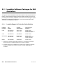
Chapter 21 984 Loadable Instructions . . . . . . . . . . . . . . 291
Loadable Software Packages for 984 Controllers . . . . . . . . . . . . . . . . . . . .
Loadable Support for Controller Option Modules . . . . . . . . . . . . . . . . . . .
Other 984 Loadable Functions . . . . . . . . . . . . . . . . . . . . . . . . . . . . . . . . . .
The 984 Hot Standby Loadable . . . . . . . . . . . . . . . . . . . . . . . . . . . . . . . . . . .
xii
Table of Contents
292
292
293
294
GM--0984--SYS
The HSBY Status Register . . . . . . . . . . . . . . . . . . . . . . . . . . . . . . . . . . . . . . .
An HSBY Reverse Transfer Example . . . . . . . . . . . . . . . . . . . . . . . . . . . . . .
CALL Blocks for the 984 Coprocessors . . . . . . . . . . . . . . . . . . . . . . . . . . . .
MBUS and PEER . . . . . . . . . . . . . . . . . . . . . . . . . . . . . . . . . . . . . . . . . . . . . . .
MBUS
.............................................
PEER
.............................................
The MBUS Get Statistics Function . . . . . . . . . . . . . . . . . . . . . . . . . . . . . . . . .
Designing Custom Loadable Functions . . . . . . . . . . . . . . . . . . . . . . . . . . . . .
Programming Considerations . . . . . . . . . . . . . . . . . . . . . . . . . . . . . . . . . . .
Sequential Control Functions . . . . . . . . . . . . . . . . . . . . . . . . . . . . . . . . . . . . .
DRUM
.............................................
ICMP
.............................................
Cascaded DRUM/ICMP Blocks . . . . . . . . . . . . . . . . . . . . . . . . . . . . . . . . . .
Extended Math Loadables . . . . . . . . . . . . . . . . . . . . . . . . . . . . . . . . . . . . . . . .
MATH
.............................................
DMTH
.............................................
2The EARS Loadable . . . . . . . . . . . . . . . . . . . . . . . . . . . . . . . . . . . . . . . . . . .
984 Functions in an Event/Alarm Recording System . . . . . . . . . . . . . . .
Host↔Controller Interaction . . . . . . . . . . . . . . . . . . . . . . . . . . . . . . . . . . . .
The EARS Block . . . . . . . . . . . . . . . . . . . . . . . . . . . . . . . . . . . . . . . . . . . . .
Index
GM--0984--SYS
296
297
298
300
300
302
304
306
307
308
308
310
311
312
312
313
317
317
317
318
. . . . . . . . . . . . . . . . . . . . . . . . . . . . . . . . . . . . . . 321
Table of Contents
xiii
Preface
The data and illustrations found in this book are not binding. We reserve the
right to modify our products in line with our policy of continuous product
improvement. Information in this document is subject to change without notice
and should not be construed as a commitment by Modicon, Inc., Industrial
Automation Systems. Modicon, Inc. assumes no responsibility for any errors
that may appear in this document.
No part of this document may be reproduced in any form or by any means,
electronic or mechanical, without the express written permission of Modicon,
Inc., Industrial Automation Systems. All rights reserved.
The following are trademarks of Modicon, Inc.:
Modbus
984B
984-680
984-380
Compact 984
P230
Modbus Plus
984X
984-485
Micro-984
AT-984
BP85
Modbus II
984-785
984-480
984-120
MC-984
SM85
984
984-780
984-385
984-130
Q984
SA85
984A
984-685
984-381
984-145
P190
MODSOFT® is a registered trademark of Modicon, Inc.
IBM® is a registered trademark of International Business Machines Corporation.
IBM AT™, IBM XT™, Micro Channel™, Personal System/2™, and NetBIOS™ are
trademarks of International Business Machines Corporation.
Microsoft® and MS-DOS® are registered trademarks of Microsoft Corporation.
Copyright © 1991 by Modicon, Inc. All rights reserved.
Printed in U. S. A.
GM--0984--SYS
Preface
iii
Chapter 1
The 984 Programmable
Controllers
Modicon’s Family of 984 Programmable Controllers
984 Controller Performance and Capacity Characteristics
How a 984 System Provides Application Control
P190-Style Panel Software Support
MODSOFT Panel Software Support
Overview of the 984 Instruction Set
GM--0984--SYS
The 984 Programmable Controllers
1
1.1
Modicon’s Family of Programmable
Controllers
Modicon offers a wide range of compact, midsize, and high-performance CPUs
with its 984 family of programmable controllers. All 984 controllers, regardless of
their particular hardware implementation, use a common processing architecture;
they are all programmed with ladder logic, a powerful and graphical language that
emulates relay-equivalent symbology; and they share common instructions drawn
from a large set of calculation, data transfer (DX), matrix, and special-application
functions. Modicon also provides you with various networking strategies, allowing
you to interconnect multiple controllers—and other devices—for increased application control and data exchange.
1.1.1
The 984 Family
984 controllers are available in four generic hardware classes:
Large, rugged, high-performance chassis mount controllers
Rugged, midrange-performance slot mount controllers, which reside in a
primary housing beside 800 Series I/O modules
Host-based controllers built on various industry-standard computer cards
designed to reside in and execute control logic from a host computer
Low-cost, easy-to-install compact controllers, for applications with less
demanding environmental and performance requirements
The family approach to 984 controller design allows you to make choices based
on controller capacity (the number of discrete and analog/register points available
for application programming, the number of I/O drops it supports), throughput (the
rate at which it solves logic and updates I/O modules), and environmental hardness (the design standards its hardware implementation must meet).
2
The 984 Programmable Controllers
GM--0984--SYS
1.1.2
Controller Compatibility
A major advantage of the family approach to 984 controller design is product
compatibility. Regardless of its computational capacity, performance characteristics, or hardware implementation, each 984 controller is architecturally consistent
with other 984s.
The 984 instruction set (the functional capabilities of the controller, part of the system firmware stored in executive PROM) comprises logic functions common to
other 984s. This means that user logic created on a midrange or high-performance unit such as a 984-685 or a 984B can be relocated to a smaller controller
such as a 984-145 (assuming sufficient memory in the smaller machine) and that
logic created on a smaller controller is upwardly compatible to a larger unit. As
your application requirements increase, it is relatively easy to upgrade your controller hardware without having to rewrite control logic.
Also, training costs and learning curves can be reduced, since users familiar with
one 984 model automatically have a strong understanding of others.
GM--0984--SYS
The 984 Programmable Controllers
3
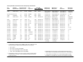
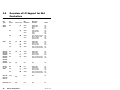
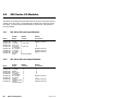
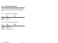
1.2
984 Controller Performance and
Capacity Characteristics
The table on the following page gives you an overview of 984 programmable controller characteristics. The 984 controller models are listed by capacity in descending order, the 24 bit CPUs first, followed by the 16 bit CPUs. The capacity
of a controller is a function of the number of discrete and register points available
in state RAM—a discrete point uses one bit while a register/analog point requires
16 bits.
Notice that the discretes and registers are implemented in two different areas of
system memory—in state RAM and in real-world I/O locations as defined by the
984 traffic cop. The registers and discretes available in state RAM may be used
for programming I/O, internal coils, and data registers; the registers and discretes
available through the traffic cop can be used only for programming local or remote
I/O points. In some of the smaller-cpacity controllers, the traffic cop limits the
maximum number of I/O bits and the total number of discrete I/O points to numbers below what is available in state RAM. The additional discretes and registers
from state RAM may be used in the logic program for internal coils and data storage buffers, but they cannot be mapped to I/O points.
4
The 984 Programmable Controllers
GM--0984--SYS
984 Programmable Controller Performance and Capacity Characteristics
984
Model
Hardware
Logic Solve CPU
Implementation (ms/Kword) Size
User
Logic Size**
State RAM
Regs
Discretes
Maximum I/O
Bits per Drop
Maximum I/O
Bits/System
Total
Discrete I/O
Max. Drops
per System
984B
Chassis mount
0.75
24 bits
32K/64K*
9999
8192***
1024 in/1024 out
256 in/256 out
32768 in/32768 out
4096 in/4096 out
8192 in/8192 out
4096 in/4096 out
32 R (S908)
16 R (S901)
984--780/--785 Slot mount
1.5
24 bits
16K/32K
9999
8192***
512 in/512 out
16384 in/16384 out
8192 in/8192 out
1 L, 31 R
Q984
Host Based
2.0
24 bits
12K
9999
8192***
512 in/512 out
3584 in/3584 out
3584 any mix
7R
984A
Chassis mount
0.75
16 bits
16K/32K
1920
2048 any mix
1024 in/1024 out
256 in/256 out
32768 any mix
4096 in/4096 out
2048 any mix
2048 any mix
32 R (S908)
16 R (S901)
984X
Chassis mount
0.75
16 bits
8K
1920
2048 any mix
512 in/512 out
3584 in/3584 out
2048 any mix
1 L, 6 R
984--685
Slot mount
2.0
16 bits
8K/16K
4096**** 2048 any mix
512 in/512 out
16384 in/16384 out
2048 any mix
1 L, 31 R
984--680
Slot mount
3.0
16 bits
8K/16K
4096**** 2048 any mix
512 in/512 out
16384 in/16384 out
2048 any mix
1 L, 31 R
AT--984
Host Based
1.5
16 bits
8K
1920
2048 any mix
512 in/512 out
3584 in/3584 out
2048 any mix
7R
MC--984
Host Based
1.5
16 bits
8K
1920
2048 any mix
512 in/512 out
3584 in/3584 out
2048 any mix
7R
984--485
Slot mount
3.0
16 bits
4K/8K
1920
2048 any mix
512 in/512 out
3584 in/3584 out
1024 any mix
1 L, 6 R
984--480
Slot mount
5.0
16 bits
4K/8K
1920
2048 any mix
512 in/512 out
3584 in/3584 out
1024 any mix
1 L, 6 R
984--385
Slot mount
3.0
16 bits
4K/6K
1920
2048 any mix
512 in/512 out
512 in/512 out
512 any mix
1L
984--381
Slot mount
5.0
16 bits
1.5K/4K/6K
1920
2048 any mix
512 in/512 out
512 in/512 out
512 any mix
1L
984--380
Slot mount
5.0
16 bits
1.5K/4K/6K
1920
2048 any mix
512 in/512 out
512 in/512 out
256 any mix
1L
984--145
Compact
4.25
16 bits
8K
1920
2048 any mix
512 in/512 out
512 in/512 out
256 any mix
1L
984--130
Compact
4.25
16 bits
4K
1920
2048 any mix
512 in/512 out
512 in/512 out
256 any mix
1L
984--120
Compact
4.25
16 bits
1.5K
1920
2048 any mix
512 in/512 out
512 in/512 out
256 any mix
1L
Micro--984
Micro
5.0
16 bits
4K
1920
2048 any mix
64 in/64 out
(112 total)
64 in/64 out
(112 total)
112 any mix
1L
R = Remote, L = Local
*
The 984B offers extended memory (XMEM) in 32K, 64K, and 96K sizes; total
memory can be up to 128K, with up to 64K devoted to user logic (UL):
•
•
•
•
**
32K = 32K UL
64K = 64K UL or 32K UL/32K XMEM
96K = 32K UL/64K XMEM or 64K UL/32K XMEM
128K = 32K UL/96K XMEM or 64K UL/64K XMEM
Approximately 1K words of user logic are used for system overhead; utilizes
one word/node for user logic—e.g., a normally open contact uses one word
of user logic memory.
4
*** State RAM in these 24 bit CPUs may be allocated as 8192 discrete I/O
+ 9999 registers or as (8192 discrete in/8192 discrete out + 8500 registers).
****
4096 registers are available if you use an Extended Register cartridge
(AS--E685--914 or AS--E680--914); otherwise, 1920 registers are available.
1.3
How a 984 System Provides
Application Control
A 984 programmable controller is a special-purpose computer with digital
processing capabilities, designed for real time control in industrial and manufacturing applications. In essence, a programmable controller monitors the state of field
devices by receiving signals from its input modules, solves a user logic program
via its CPU component, and directs further field device activity by sending control
signals to its output modules.
1.3.1
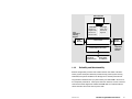
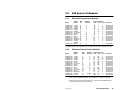
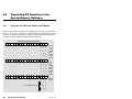
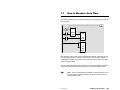
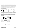
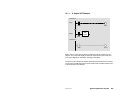
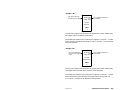
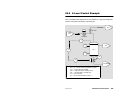
The 984 Control Architecture: An Overview
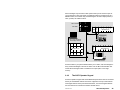
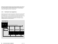
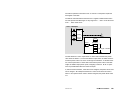
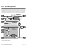
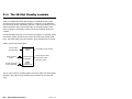
All controllers in the 984 family share a common processing architecture, which
comprises:
A memory section that stores user logic, state RAM, and system overhead in
battery-backed CMOS RAM and holds the system’s Executive firmware in
nonvolatile ROM
A CPU section that solves the user logic program based on the current input
values in state RAM, then updates the output values in state RAM
An I/O processing section that directs the flow of signals from input modules to
state RAM and provides a path over which output signals from the CPU’s logic
solve are sent to the output modules
A communications section that provides one or more port interfaces. These interfaces allow the controller to communicate with programming panels, host
computers, hand-held diagnostic tools, and other peripheral (master) devices
as well as with additional controllers and other nodes on a communications
network
6
The 984 Programmable Controllers
GM--0984--SYS
984 Controller
CPU
Memory
from
Application
Sensing
Devices
Input
Modules
State RAM
Register Ins
Register Outs
Discrete Ins
Discrete Outs
User Logic
Ladder logic
networks &
segments
I/O Processor
Communications Processor
Peripheral
(Host) Devices
1.3.2
Output
Modules
to
Application
Switching
Devices
Other Nodes
on a Network
Reliability and Maintainability
Modicon designs fault protection and isolation features into all 984 controllers.
Orderly system startup and shutdown procedures help protect system memory,
state RAM, and system hardware from damage due to external power failures.
Long-life lithium batteries back up system memory and state RAM in the event of
an unexpected power failure. When power has been restored, a series of internal
controller checksum diagnostics validate that RAM data are consistent with the
values that were active at the time of power-down.
GM--0984--SYS
The 984 Programmable Controllers
7
1.4
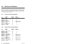
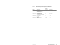
P190-Style Panel Software Support
Modicon provides P190 panel software (SW-CS9T-0TB) on specially constructed
cassette tapes, and P190 emulation software on 5.25 in (SW-CS9D-5DA) and
3.5 in (SW-CS9D-3DA) diskettes for the P230 Programming Panel or for IBM-XT,
-AT, or compatible Personal Computers.
1.4.1
Standard Panel Software Editors
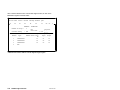
Standard panel software packages contain the following editors:
Software
Editor
3.5 in
Diskette
5.25 in
Diskette
P190
Tape
Editor
Description
Configurator
Defines control and communication parameters, allocates memory, accesses controller operations
Traffic Cop
Links discrete and register reference numbers to locations in the I/O subsystems
Programmer
Generates, edits, monitors ladder logic, and
accesses controller operations
ASCII
Programmer
Generates and edits ASCII-formatted
messages
LRV
Loads programs from disk to controller,
records 984 memory to disk, compares programs on disk and in memory
Tape Loader
Records user logic on tape, loads programs
to 984 memory, compares programs on tape
and in memory
Ladder Lister
Generates hard copy of user logic program
Annotated
Ladder Lister*
Prints user comments along with hard copy
of the user logic program
Utility
Accesses controller memory, prints ladder
listing, accesses controller operations
Executive
Overview menu for PC programming
software
*
8
There is no editor feature comparable to the Annotated Ladder Lister in the P190 Panel
Software package.
The 984 Programmable Controllers
GM--0984--SYS
1.4.2
Special Loadable Software
Additional loadable software is available to support optional controller hardware
and special purpose applications:
Software
Loadable
3.5 in
Diskette
5.25 in
Diskette
P190
Tape
Program
Description
HSBY
Enables switchover of controller functions to
a back-up controller without downtime
CALL
Expands controller’s processing capabilities
by calling C functions from a Coprocessor
library
MBUS/PEER
Enables peer-to-peer communications via
Modbus II
PID2**
Enables configuring, tuning, and monitoring
of closed loop control system
MSTR* **
Provides Modbus Plus capabilities via the
S985 option module
DRUM/ICMP
Simplifies implementation of sequential step
oriented logic
Advanced
Math/DX*
Provides enhanced math and data transfer
capabilities
EARS
Provides an event/alarm reporting system
that detects and time-stamps changes in
events, and places the data in a controller
buffer where it can be accessed by a host
computer or high speed network
*
Advanced math functions include log, antilog, square root, process square root,
and double precision math; advanced DX functions include table-to-block and
block-to-table moves and checksum.
** PID2, MSTR, and the advanced math DX functions are provided as loadables for the
chassis mount controllers only; comparable functionality is provided as standard in
other controllers (see Section 1.6).
For more details on the loadable software packages, see Chapter 21.
GM--0984--SYS
The 984 Programmable Controllers
9
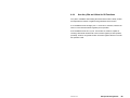
1.5
MODSOFT Panel Software Support
MODSOFT is an integrated software tool for programming, testing, and documenting application logic for 984 controllers that may be used on a P230 Programming Panel or on an IBM-XT, -AT, or compatible Personal Computer. All the
editor functions available in the P190 and P190 emulation packages are combined
in MODSOFT along with enhanced features. MODSOFT comprises a set of
source code editors for programs and for symbolic information. The source programs are subdivided into SFC language and ladder logic.
1.5.1
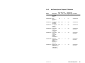
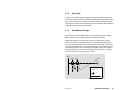
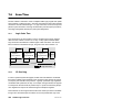
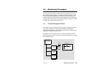
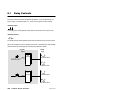
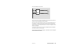
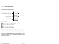
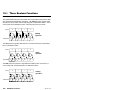
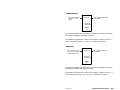
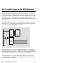
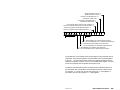
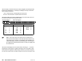
Sequential Function Charts
SFC is an optional feature that allows you to generate new programs arranged in
blocks rather than the linear sequence of straight ladder logic. A sequential function chart can solve multiple networks in a parallel link block or one in a choice of
several networks in a selective link block.
Initial Step
S011
S = Step
T = Transition
1
T
011
Parallel Link
S021
S022
S023
2
T
2
S024
2
021
S031
T
S041
T
031
6
041
T
S042
T
1
032
3
042
S011
10
2
T
033
Selective Link
S043
T
1
043
Reference (goto)
The 984 Programmable Controllers
GM--0984--SYS
Logic is solved within a block until a specified transition event informs the CPU to
move to the next step. SFC allows application software to be created in a format
that more closely emulates an actual machining procedure or process flow; it can
help improve system throughput by solving only those networks specified by transition events rather than moving linearly through each network in the program on
every scan.
1.5.2
MODSOFT Macros
MODSOFT provides a macro feature that can simplify the task of generating and
updating large number of repetitive network structures. Using the macro feature,
you can create the repeating structure once, then specify the node values using
macro parameters rather than standard 984 reference numbers. Each macro can
contain up to 66 macro parameters—by using ∗ wild card characters in your naming scheme, you can actually create thousands of parameters/macro.
1.5.3
MODSOFT Operating Modes
You may operate in three modes in MODSOFT:
Offline, where programming and programming modification can be done without using a 984 controller linked to the programming device
Online, where the application is communicating with the controller and any
changes made to the program are reflected in the controller
Debug, where any changes made to the logic program are saved simultaneously in the 984 controller and in the offline program file and where SFC can
be monitored for power flow
GM--0984--SYS
The 984 Programmable Controllers
11
1.6
Overview of the 984 Instruction Set
The following instructions are standard in all 984 System Executives:
Instruction
Meaning
Normally open contact
Normally closed contact
↑
↓
( )
(L)
Positive transitional contact
Negative transitional contact
Coil
Latch coil
Calculations Functions
ADD
Addition
SUB
Subtraction, greater than, less than, and equal to
MUL
Multiplication
DIV
Division
Counting & Timing Functions
UCTR
Up counter from 0 to a preset
DCTR
Down counter from a preset to 0
T1.0
Timer that increments in seconds
T0.1
Timer that increments in tenths of a second
T.01
Timer that increments in hundredths of a second
Data Transfer (DX) Move Functions
Register-to-table move
R→T
T→ R
Table-to-register move
T→ T
Table-to-table move
BLKM
Block move
FIN
First-in operation to a queue
FOUT
First-out operation from a queue
SRCH
Table search
STAT
Programmable controller health status
DX Matrix Functions
AND
OR
XOR
COMP
CMPR
MBIT
SENS
BROT
SKP
12
Logical AND of two matrices
Logical inclusive OR of two matrices
Logical exclusive OR of two matrices
Logical complement of one matrix
Logical compare of two matrices
Logical bit modify
Logical bit sense
Logical bit rotate
A skip function
The 984 Programmable Controllers
GM--0984--SYS
The following instructions may be available in standard executive, loadable, or
executive upgrade form, depending on controller type:
Instruction
Meaning
TBLK
BLKT
PID2
Moves a block of data from a table to another specified block area
Moves a block of registers to specified locations in a table
Performs proportional-integral-derivative control functions
The following are standard in some Executives and unavailable in others:
Instruction
Meaning
Available with 984s that Support Remote I/O
READ
Reads data from an ASCII device to 984 memory
WRIT
Sends data from a 984 to an ASCII device
Available in 984s with Extended Memory
XMRD
Reads function for 984s with Extended Memory
XMWT
Writes Extended Memory data
Available in 984s with Modbus Plus Capabilities
MSTR
Reads, writes, and gets status of MB+ network operations
Available in 984s with Subroutines Capabilities
JSR
Jumps the CPU from scheduled logic to a ladder logic subroutine
LAB
Labels the entry point for a ladder logic subroutine
RET
Returns the CPU from a subroutine to scheduled ladder logic
Unavailable in Chassis Mount Controllers
EMTH
Performs extended math functions—square root, process square
root, log, antilog, and floating point functions
Unavailable in Controllers that Support Modbus Plus
CKSM
Performs CRC-16, LRC, straight, or binary add checksum functions
The following are available as loadables in some controllers:
Instruction
Meaning
HSBY
MBUS, PEER
CALL
DRUM, ICMP
MATH, DMTH
FNxx
EARS
Supports a Hot Standby control system
Supports Modbus II read/write/status capabilities
Supports C986/C996 Coprocessor capabilities
Support drum sequencer applications
Perform some extende math functions in 984s that don’t use EMTH
Supports a user-developed library of custom loadable functions
Supports an event/alarm reporting system
For more details regarding loadable instructions, see Chapter 21.
GM--0984--SYS
The 984 Programmable Controllers
13
Chapter 2
Optional and Peripheral
Control Devices
Programming Panels
The P965 Data Access Panel
The Hot Standby Option Modules
The Coprocessing Option Modules
Optional Communication Modules
GM--0984--SYS
Optional and Peripheral Control Devices
15
2.1
Programming Panels
Modicon offers two kinds of industrially hardened programming panels—the P230
and the P190. These panels may be used to:
Start and stop the controller
Enter, modify, and archive ladder logic programs
Monitor the register and discrete values in user memory and state RAM
Enable, disable, and force discrete inputs and coils
Display and modify the contents of holding registers
Display and set communication parameters for the communication ports
Provide on-line monitoring of power flow
2.1.1
The P230
The AS-P230-000 is a portable programming panel with a 40 Mbyte hard disk formatted and installed with MS-DOS and GW-BASIC interpreter software. It supports both MODSOFT and P190 emulation software, either of which may be
loaded from the unit’s a 3.5 in disk drive. The P230 power supply is 115/230 VAC
user-selectable.
16
Optional and Peripheral Control Devices
GM--0984--SYS
2.1.2
The P190 Panels
The P190 is a Modicon-proprietary portable programming panel software with a
set of specially designed digital tapes (see section 1.4) for use specifically in this
panel. The P190 does not support the MODSOFT. There are two types of P190
Panels available—the AS-P190-212, which operates on 115 VAC, and the
AS-P190-222, which operates on 220 VDC.
2.1.3
Using Industry-standard PCs as Programming Panels
A set of 5.25 in and 3.5 in disks is available to emulate the P190 software on a
standard DOS-based PC, and the integrated MODSOFT package is also available
on both 5.25 in and 3.5 in distribution disks. These software packages can be run
on any IBM-AT or true AT-compatible PC.
GM--0984--SYS
Optional and Peripheral Control Devices
17
2.2
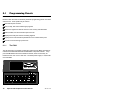
The P965 Data Access Panel
The AS-P965-000 Data Access Panel (DAP) is a hand-held troubleshooting device. It connects to a Modbus port (or ASCII/DAP port on a 984A or 984B) on any
Modicon controller that supports Modbus communication.
2.2.1
Physical Design
The P965 DAP is a lightweight device with a 64-character liquid crystal display
(LCD) screen and a keypad with alphanumeric and function keys.
18
Optional and Peripheral Control Devices
GM--0984--SYS
2.2.2
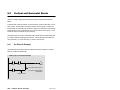
How the P965 Can Be Used
A P965 DAP is a very effective tool for monitoring and troubleshooting the controller. With it, you can
Start and stop the controller
Monitor the register and discrete values in user memory and state RAM
Enable, disable, and force discrete inputs and coils
Display and modify the contents of holding registers
Display and set communication parameters for the Modbus ports
The P965 can be used on the shop floor to monitor the status of a 984 programmable controller by accessing the STAT block. (Procedures for accessing the
STAT block are described in Sections 14.4 and 14.10; the types of statistics available from the STAT block are described in detail in Section 14.5 ... 14.7 for an
S901 RIO network and Sections 14.11 ... 14.13 for other 984 I/O networks.
GM--0984--SYS
Optional and Peripheral Control Devices
19
2.3
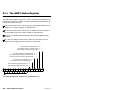
The Hot Standby Option Modules
The Hot Standby capability has been designed for applications that demand
fault-tolerant, high-availability performance. Two identically configured 984 controllers communicate with each other through two Hot Standby option modules,
one in each controller. Each controller has the HSBY loadable software function
block installed in the first segment of ladder logic (described in Chapter 21).
2.3.1
How a Hot Standby System Functions
AM-R911-000 Hot Standby option modules are designed for use in a system involving two identically configured chassis mount controllers. AS-S911-800 Hot
Standby option modules are designed for use in a system involving two identically
configured 984-680, -685, -780, or -785 slot mount controllers.
Upon powering up a 984 Hot Standby system, one of the two identically configured 984 controllers acts as the primary controller—it reads input data from remote I/O drops, executes the stored user programs from memory, and sends appropriate output commands to the drops. The primary controller updates the
standby controller with current system and state RAM status information at the
end of each scan.
The standby controller only reads this information—it does not execute control
functions and does not interfere with primary control operations. It will assume
primary system control in 13 ... 48 ms if the primary controller fails.
2.3.2
Controller Compatibilities
The S911 and R911 Hot Standby modules are devices designed to be installed in
option slots with their host controllers. They work in conjunction with 984 controllers that use S908 Remote I/O Processor modules. The R911 modules work with
the 984A, 984B, and 984X chassis mount Controllers; the S911 modules work
with 984-68x and 984-78x slot mount Controllers. All hardware and firmware in
the primary and standby controllers must be identical.
20
Optional and Peripheral Control Devices
GM--0984--SYS
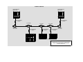
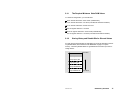
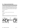
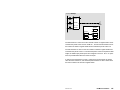
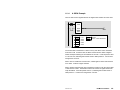
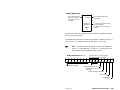
The two Hot Standby modules in a system are interconnected by a AS-W911-0xx
cable, and the coaxial cables running from the two S908 RIO Processors pass
through self-terminating connectors before being joined by an MA-0186-100 line
splitter.
S
9
0
8
984 Controller
(Primary)
S/R
9
1
1
984 Controller
(Standby)
S
9
0
8
S/R
9
1
1
W911
Coax
52-0370-000 75
60-0513 75
TR-75F 75
Ω Self-terminating Connector
Ω Feed-through Terminator
Ω
J
8
9
0
800
Series
I/O
J
8
9
2
800
Series
I/O
Cable Terminator
MA-0186-100 Line Splitter
MA-0185-100 Line Tap
GM--0984--SYS
P
200
4
Series
5
I/O
3
with
J290
Optional and Peripheral Control Devices
21
2.4
The Coprocessing Option Modules
Modicon offers two types of integrated control processors (Copros)—the C986 for
use with chassis mount 984 controllers and the C996 for use with slot mount 984
controllers that support option modules. These option modules extend the processing capabilities of your controller, providing alternative programming solutions
for problems that are difficult or inefficient to handle via ladder logic.
2.4.1
The C986 Copro for Chassis Mount 984s
The AM-C986-004 Copro resides in a single option slot in a 984A, 984B, or 984X
chassis. It uses the flexible, multitasking VRTX Operating System, which allows
it to perform parallel application processing, immediate DX processing, and
deferred DX processing (see Section 2.5). Programs developed in Microsoft C,
either by you or by Modicon, can be downloaded to the Copro and run in parallel
with the 984 CPU.
Green READY LED indicates the system is scanning
Green STATUS 1 LED goes ON when the 984 is communicating
with the C986
Green STATUS 2 LED goes ON when the C986 is under user
software control
Red BATTERY LOW LED indicates that the battery needs replacing
Nine-pin D-shel subminiature receptacles that can be configured
for RS-232C or RS-422
22
Optional and Peripheral Control Devices
GM--0984--SYS
2.4.2
The C996 Copros for Slot Mount 984s
Two coprocessor models are available for use with slot mount controllers—the
AM-C996-802 Copro with two expansion slots and the AM-C996-804 Copro with
four expansion slots. These copros are DOS-based computer systems with a proprietary high speed interface to 984 controller memory. The C996 Copros can
perform parallel application processing and immediate DX processing, but not deferred DX processing (see Section 2.5).
The AM-C996-802 consumes one and a half slots in a slot mount controller housing, and the AM-C996-804 consumes two and a half slots in the housing.
Green READY LED goes ON after power-up to indicate
that the device driver is loaded; other uses of this LED
are application-dependent
Green STATUS LED is application-dependent
Two 9-pin serial ports, fully programmable for
asynchronous communication
A 37-pin floppy drive interface
A keyboard port programmed to support a serial
interface to an AT or AT-compatible keyboard
AM-C996-802
AM-C996-804
The expansion slots can support various commercially available option cards.
The depth dimension of the C996 expansion slots limits your choice of option
cards to half-size IBM-XT cards.
GM--0984--SYS
Optional and Peripheral Control Devices
23
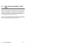
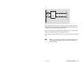
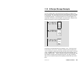
2.5
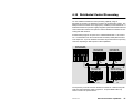
Enhancing Your Processing
Environment with a Copro
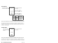
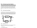
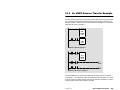
Both the VRTX-based C986 Copro and the DOS-based C996 Copros can communicate with the controller in two different modes—application mode and immediate DX mode. Only the C986 Copro can communicate with the controller in
deferred DX mode.
2.5.1
Application Mode
The C986 and C996 Copros can run programs in application mode in parallel with
the 984 CPU, exchanging data with the controller at the end of scan (EOS):
SCAN 1
SCAN 2
EOS
984 CPU
Interrupt
COPRO
Logic
Scanning
Application
Processing
How a Copro Handles Application Processing in Parallel with the 984 CPU
2.5.2
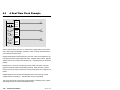
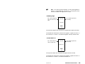
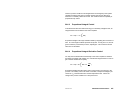
Immediate DX Processing
The C986 and C996 Copros can run standard and customized C routines that are
initiated, or called, by ladder logic—a loadable CALL function block (described in
Chapter 21) is provided for this purpose.
24
Optional and Peripheral Control Devices
GM--0984--SYS
When a Copro suspends application processing for a short interval and dedicates
itself to the solution of a CALL function, it is performing in immediate DX mode. A
typical immediate DX function might be a floating point math calculation.
SCAN 1
CALL
to
IMMDX
SCAN 2
EOS
984
CPU
COPRO
How a Copro Handles Immediate DX Processing
2.5.3
Deferred DX Processing
Because of the multitasking capability inherent of the VRTX Operating System,
the C986 can also call deferred DX functions simultaneously with application and
immediate DX processing. Up to ten tasks can be supported.
In deferred DX mode, DX processing begins with a call and continues until it is finished, even if its processing runs longer than one scan. A typical deferred DX
function might be reading bar code input to a serial port.
SCAN 1
CALL
to
DEFDX
SCAN 2
EOS
984
CPU
COPRO
How the C986 Copro Handles Deferred DX Processing
GM--0984--SYS
Optional and Peripheral Control Devices
25
2.6
Optional Communication Modules
984 Controllers may be interconnected in various kinds of local area (and in some
cases long distance) networks. The following 984 controller option modules that
allow you to establish the network connections are described here; overall networking capabilities are described in more detail in Chapter 4.
2.6.1
Modbus Modems
The AM-S978-000 Dual Modbus Modem is an option module that allows a chassis
mount 984 controller to be used as a slave processor in a Modbus network. The
AS-J878-000 is an option module that provides similar capability in a slot mount
984 controller. These Modbus modems allow you to create Modbus networks up
to 15,000 ft (4572 m) long and comprising up to 247 slave nodes.
These modems are electrically compatible with all Modbus products and are sized
to fit in one slot (in a 984 chassis in the case of the S978 and in an 800 Series I/O
primary housing in the case of the J878). The S978 module contains two modems, which are connected via cable to Modbus ports on the comm processor
module in the controller; the J878 module contains one modem.
An S978 Modem accepts digital data from the slave controller in which it resides
and modulates the data into an FM analog signal—a form of transmission suited
to four-wire cable. It transmits the analog FM signal to the host’s Modbus Master
device, where it is demodulated to digital data. Conversely, the Modbus Master
transmits digital data, which is modulated to an FM analog signal on its way back
to the S978 Modem. The S978 demodulates the analog signal to digital data and
sends the data to the slave controller in which it resides.
For more information about Modbus network capabilities, see Section 4.6.
2.6.2
Modbus II Modules
The S975 Modbus II Interfaces are option modules that allows a 984 controllers to
be used as a processing node in the Modbus II network. The AM-S975-100 mod-
26
Optional and Peripheral Control Devices
GM--0984--SYS
ule may be used with any chassis mount controller, and the AM-S975-820 module
may be used with 984-685, -780, or -785 slot mount controllers.
Modbus II provides peer-to-peer communication capabilities between 984 controllers and other Modbus II devices over a local area network. For more information
about Modbus II networking, see Section 4.9.
Special software must be loaded into the controller to program Modbus II communications in ladder logic. Two loadable function blocks—MBUS and PEER (described in Chapter 21)—are used to initiate communications. MBUS writes information to or reads information from a single controller. PEER writes register
information to up to 16 controllers simultaneously.
2.6.3
The Modbus Plus Options
Several 984 controllers have a Modbus Plus capability built directly into the controller—i.e, the slot mount 984-385, 984-485, 984-685, and 984-785 Controllers,
the Compact 984-145 Controller, and the host based AT-984 and MC-984
Controllers.
For the chassis mount controllers and for the slot mount controllers that accept
option modules (the 984-68x and -78x ), various S985 Modbus Plus Adapter
cards are available as option modules. An S985 comes with a loadable version of
the MSTR function block (described in Chapter 17), which allows you to initiate
Modbus Plus communication functions; in 984 controllers with built-in Modbus
Plus capabilities, the MSTR function is part of the standard executive firmware.
The AM-S985-000 card is used with a 984X Controller, the AM-S985-020 is used
with a 984A Controller (with an S908 RIOP), and the AM-S985-040 is used with
the 984B Controller (with an S908 RIOP).
2.6.4
The Distributed Communications Option
The AS-D908-110 and AS-D908-120 Distributed Control Processors allow you to
extend programmable control capabilities over the S908 remote I/O link. These
option modules allow entire 984 control systems (CPU and I/O) to appear as remote I/O drops on a higher level remote I/O link. The distributed link is described
in Section 4.10.
GM--0984--SYS
Optional and Peripheral Control Devices
27
The D908 modules may be used with a 984-680, -685, 780, and -785 slot mount
controllers installed at remote locations and connected to a higher level 984 controller via the S908 remote I/O cable. The higher level controller sees this distributed controller as a J890 remote I/O drop. The D908-110 option module supports
one cable connection; the D908-120 supports two connections.
28
Optional and Peripheral Control Devices
GM--0984--SYS
Chapter 3
984 I/O Subsystems
I/O Subsystems
Local I/O
Remote I/O
ASCII Communication at Remote I/O Drops
Overview of I/O Support for 984 Controllers
800 Series I/O Modules
Power Supplies for Local and Remote 800 Series I/O Drops
200 Series I/O Modules
500 Series I/O Modules
A120 Series I/O Modules
300 Series I/O Modules
GM--0984--SYS
984 I/O Subsystems
29
3.1
I/O Subsystems
The application logic that is stored in and solved by the controller is implemented
on the factory floor by input and output modules. These I/O modules are fieldwired to sensing or switching devices on the shop floor and linked to the controller
over an I/O bus to create a complete control system. Modicon provides several
series of I/O modules that may be implemented by different 984 controllers.
3.1.1
Input and Output Modules
An input module accepts electrical signals from field sensing devices, isolates
these signals from the controller, and converts them into acceptable voltage levels
that update the controller’s State RAM.
An output module accepts electrical signals from the controller’s state RAM, isolates these signals from the field, and converts them into voltage or current levels
necessary to activate working devices or indicator displays on the factory floor.
3.1.2
I/O Module Types
Input and output modules are wired to industrial field devices that send or receive
application data. When you plan your I/O layout, match the electrical signal used
in the I/O modules with the signal used by the field device to which it is wired.
Modicon offers a wide range of I/O modules:
Discrete in, which convert signals coming from field input devices such as pressure switches, limit and proximity switches, or photo sensors into voltage levels
that can be used by the controller
Discrete out, which convert voltage levels generated by the controller’s logic
solving into output signals used by output field sensing devices such as relays,
lamps, or solenoids
Discrete input and output modules are available to support AC, DC, and TTL
field input devices
Analog in, which convert analog input signals coming from field input devices
such as pressure, level, temperature, or weight sensors into numerical data
30
984 I/O Subsystems
GM--0984--SYS
that can be used by the controller—this numerical data ranges from 0000 to
4095
Analog out, which convert numerical data generated by the controller’s logic
solving into analog output signals to be used by output field devices—such as
heaters or pumps
Special purpose, designed for unique field applications such as multiplexing,
high speed counting, and temperature reading
Intelligent, designed for unique field applications requiring bidirectional (in/out)
capabilities and on-board processing power
3.1.3
Local and Remote I/O
I/O subsystems may be local—located together with or in close proximity to the
controller—or remote—located at distances up to 15,000 ft (4.5 km) from the controller, depending on the cable type.
GM--0984--SYS
984 I/O Subsystems
31
3.2
Local I/O
When local I/O is supported, it consists of one drop only, always designated as
drop #1 in your system configuration. Your controller restricts you to one specific
series of I/O modules at the local drop.
984 Controllers that
Support Local I/O
Local I/O
Supported
I/O-to-Controller
Connectivity
Local Devices
Supported
984X
800 Series I/O
I/O in secondary 800
Series housings* up
to 12 ft from controller, connected by
W929 cable
Up to five housings
supported
984-780, -785
800 Series I/O
In the primary 800
Series I/O housing
with controller
Up to five housings
supported
984-680, -685
800 Series I/O
In the primary 800
Series I/O housing
with controller
Up to five housings
supported
984-480, -485
800 Series I/O
In the primary 800
Series I/O housing
with controller
Up to two housings
supported
984-380, -381, -385
800 Series I/O
In the primary 800
Series I/O housing
with controller
Up to two housings
supported
Micro-984
300 Series I/O
Built-in I/O bus with
side-to-side connec-
Up to 14 I/O
modules supported
tors between controller
and other modules
984-120, -130, -145
*
32
A120 Series I/O
In primary DTA housing with controller
Up to 18 I/O
modules supported
in up to four DTA
housings
Because the I/O modules reside in a separate housing from the 984X Controller, the I/O
modules must receive their power from one or more independent slot mount power supply modules.
984 I/O Subsystems
GM--0984--SYS
3.3
Remote I/O
When remote I/O is supported, the 984 controller may support several drops—in
some cases as many as 32. In a remote I/O configuration, an RIO processor in
the controller is connected via a coaxial cable system to an RIO interface device
at each remote drop.
All 984 controllers that support remote I/O have been designed to drive 800 Series I/O at the remote drops. Several option modules and/or field modification kits
are available that allow you to drive installed bases of 200 and 500 Series I/O at
remote drops as well.
3.3.1
Remote I/O Drop Interfaces
At each remote drop is a remote I/O (RIO) interface device that communicates
over the coaxial cable with the RIO processor in the controller. The RIO interface
passes data to and from the I/O modules in the drop over the I/O housing backplane and passes data to and from the 984 controller over the RIO cable system.
An RIO interface also contains a set of switches that you use to address all the
drops in your system.
There are various kinds of RIO Interfaces you can use, depending on the I/O Series in the drop and the type of RIO processor in the controller. According to your
application requirements, you may select RIO Interfaces that provide the drop with
ASCII device support.
For a detailed discussion of the planning, installing, and testing an RIO cable system, refer to the Modicon Remote I/O Cable System Planning Guide
(GM-0984-RIO).
GM--0984--SYS
984 I/O Subsystems
33
3.4
ASCII Communication at the Remote
I/O Drops
A 984 Controller that communicates with remote I/O allows you to connect ASCII
data entry and data display devices at as many as 16 drop sites. Special types of
remote I/O interface devices must be used at drops when ASCII devices are used.
3.4.1
RIO Interfaces that Support ASCII Communication
The J812 and J892 Remote I/O Interfaces (for 800 Series I/O) and P453 Remote
I/O Interface (for 200 and 500 Series I/O) have 25-pin female ASCII ports; the
P892 RIO Interface (for 800 Series I/O) has 9-pin female ASCII ports:
25-Pin Male
RIO ASCII Port
(J812, J892, P453)
9-Pin Male
RIO ASCII Port
(P892)
SHIELD
1
SHIELD
1
TX
2
RX
2
RX
3
TX
3
RTS
4
DTR
4
CTS
5
GROUND
5
DSR
6
DSR
6
7
RTS
7
20
CTS
8
GROUND
DTR
Each of these RIO Interface devices can support two ASCII devices. As many as
32 ASCII devices can be run from a 984 controller, two/drop from up to 16 drops.
3.4.2
ASCII Device Programming
Two three-node function blocks—READ and WRIT—are provided in the Executive
PROM of all 984 controllers with RIO capabilities. The function blocks are implemented in user logic to handle ASCII message passing between the remote
devices and controller memory.
34
984 I/O Subsystems
GM--0984--SYS
ASCII messages may be written to 984 system memory from an ASCII input device (a keyboard, a bar code reader, a pushbutton panel) at a remote drop via a
READ function; the controller may send messages to an ASCII display device (a
CRT, a printer) via a WRIT function.
984 Controller
with S908
P/S
ASCII Input Keyboard
and Display Terminal
200 Series I/O
J
8
9
2
800 Series I/O
ASCII Keypad
P
8
9
2
800 Series I/O
P453 with J290
ASCII Paper Printer
An ASCII editor in your panel software allows you to create, edit, and manage a library of ASCII messages to be read or written over the RIO communication link.
These ASCII messages reside in a table that occupies space in user logic
memory.
3.4.3
The ASCII Operator Keypad
An ASCII Operator Keypad with an AS-KPPR-000 option board can be connected
directly to an S908 RIO network and can be cofigured as a drop on that network.
This keypad has two ASCII ports associated with it, one as the keypad interface
and one that can be connected to another external device.
GM--0984--SYS
984 I/O Subsystems
35
3.5
Overview of I/O Support for 984
Controllers
984
Type
I/O
Series
984A,
984B
800
Local RIO
RIO
Processor
RIO Drop
Interface
ASCII
S908
J890/P890
J892/P892
J810
J812
P451 & J291
P453 & J290
P451
P453
P451 & J291 w J540
453 & J290 w J540
P451 w J540
P453 w J540
No
Yes
No
Yes
No
Yes
No
Yes
No
Yes
No
Yes
J890/P890
J892/P892
P451 w J291
P453 w J290
P451 w J540 & J291
P453 w J540 & J290
No
Yes
No
Yes
No
Yes
J890/P890
J892/P892
P451 w J291
P453 w J290
P451 w J540 & J291
P453 w J540 & J290
No
Yes
No
Yes
No
Yes
S901
200
S908
S901
500
S908
S901
984X
984-785,
984-780,
984-685,
984-680,
984-485,
984-480
984-385,
984-381,
984-380
AT-984,
MC-984,
Q984
984-120,
984-130,
984-145
800
S929
200
S929
500
S929
800
S908
200
S908
500
S908
800
N/A
N/A
No
800
N/A
200
S908
500
S908
J890/P890
J892/P892
P451 w J291
P453 w J290
P451 w J540 & J291
P453 w J540 & J290
No
Yes
No
Yes
No
Yes
A120
N/A
N/A
No
N/A
N/A
No
Micro-984 300
36
984 I/O Subsystems
GM--0984--SYS
3.6
800 Series I/O Modules
3.6.1
800 Series Discrete Input Modules
Voltage
Range
Model
Disc.
Ins
AS-B803-008
AS-B805-016
AS-B807-032
AS-B809-016
AS-B817-116
AS-B817-216
AS-B821-008
AS-B825-016
AS-B827-032
AS-B829-116
AS-B833-016
AS-B837-016
AS-B849-016
AS-B853-016
115VAC
8
115VAC
16
115VAC
32
230VAC
16
115VAC
16
230VAC
16
10...60VDC 8
24VDC
6
24VDC
32
5V TTL
16
24VDC
16
24VAC/DC 16
48VAC/DC 16
115VAC
16
125VDC
AS-B881-001* 24VDC
16
Number/
Common
Power Draw (mA)
+5.0V +4.3V -5.0V
Connector
1
8
8
8
1
1
2
8
32
16
8
8
8
8
27
40
80
42
25
25
27
27
30
27
27
40
40
40
1
1
2
1
25
25
1
2
1
1
2
1
1
1
2
14
0
15
8
8
0
0
0
0
0
15
15
15
AS-8534-000
AS-8535-000
AS-8535-000
AS-8534-000
AS-8535-000
AS-8535-000
AS-8534-000
AS-8534-000
AS-8535-000
AS-8534-000
AS-8534-000
AS-8534-000
AS-8534-000
As-8534-000
16
30
1
0
As-8534-000
*The B881 Module must be addressed as one register IN (3x) and one register OUT (4x).
3.6.2
800 Series Discrete Output Modules
Model
Voltage
Range
Disc.
Outs
Number/ Power Draw (mA)
Common +5.0V +4.3V -5.0V
Connector
AS-B802-008
AS-B804-016
AS-B806-032
AS-B808-016
AS-B810-008
AS-B814-108
AS-B820-008
AS-B824-016
AS-B826-032
AS-B828-016
AS-B832-016
AS-B836-016
AS-B838-032
AS-B840-108
AS-B881-108
AS-B882-032
115VAC
115VAC
115VAC
230VAC
115VAC
Relay
10...60VDC
24VDC
24VDC
5V TTL
24VDC
12...250VDC
24VDC
Reed Relay
120 VAC
24 VDC
8
16
32
16
8
8
8
16
32
16
16
16
32
8
8
32
2
8
8
8
1
1
2
8
32
16
8
1
8
1
optional
8
AS-8534-000
AS-8534-000
AS-8535-000
AS-8534-000
AS-8534-000
AS-8534-000
AS-8534-000
AS-8534-000
AS-8535-000
AS-8534-000
AS-8534-000
AS-8535-000
AS-8535-000
AS-8534-000
AS-8535-000
AS-8535-000
*
76
76
210
76
50
107
90
32
90
32
32
50
160
67
285*
300**
240
480
1
480
240
800
80
260
1
220
235
603
1
400
240
10
0
0
N/A
0
0
0
0
0
0
0
0
0
0
0
0
0
When all outputs are ON, power draw at +5 V is 285 mA maximum on the
B881-108; when all outputs are OFF, power draw at +5 V is210 mA maximum.
** When all outputs are ON, power draw at +5 V is 300 mA on the B882-032; when
all outputs are OFF, power draw is 200 mA.
GM--0984--SYS
984 I/O Subsystems
37
3.6.3
800 Series Analog Input Modules
Application
Ranges
Analog
Inputs
Power Draw (mA)
+5.0V +4.3V -5.0V
AS-B873-001
4...20mA;
1...5V
4
300
300
0
AS-8533-002
(Included)
AS-B873-002
-1...+10V
4
300
300
0
AS-8533-002
(Included)
AS-B875-002
4...20mA;
1...5V
4
300
300
0
AS-8533-002
(Included)
AS-B875-012
-10...+10V
4
300
300
0
AS-8533-002
(Included)
AS-B875-101
4...20mA;
-10...+10;
-5...+5V;
0...10V;
0...5V; 1...5V
8
650
975
0
AS-8533-004
(Included)
AS-B875-111
0...5V, 1...5V
-5...+5V,
0...10V,
-10...10V,
0...2mA,
0.4...2mA,
-2...+2mA
8 Differential
500
16 Single-ended
900
0
AS-8535-000
(included)
Model
3.6.4
Connectors
800 Series Analog Output Modules
Model
Application
Ranges
AS-B872-100
4...20mA
4
800
5
0
AS-8535-000
(included)
AS-B872-200
0...5V, 0...10V
-5...+5V,
-10...+10V
4
800
5
0
AS-8535-000
(included)
38
Analog
Outputs
984 I/O Subsystems
Power Draw (mA)
+5.0V +4.3V -5.0V
Connectors
GM--0984--SYS
3.6.5
800 Series Special Purpose I/O Modules
Power Draw (mA)
+5.0V +4.3V -5.0V
Addressable
Registers(I/o) Connector
Model
Description
AS-B846-001
MUX:
16 Voltage
Inputs
65
1
0
0/1
AS-8535-000
AS-B846-002
MUX:
16 Current
Inputs
65
1
0
0/1
AS-8535-000
AS-B864-001
TTL Register:
8 outputs;
8/common
220
180
0
0/8
AS-8535-000
AS-B865-001
TTL Register:
8 inputs;
8/common
400
600
0
8/0
AS-8535-000
AS-B882-239
High Speed
Counter:
2 UpCounts
0...30kHz
188
0
0
2/2
AS-8533-005
(Included)
AS-B883-001
High Speed
Counter:
2 Up/Down
Counts:
0...50kHz;
Internal Clock
680
0
0
3/3
52-0325-000
(Included)
AS-B883-200
Reads ten
300
Thermocouple
Inputs:
Types B,E,J,K,
R,S,T,N, or
linear mV
0
0
3/3
52-0325-000
(Included)
AS-B883-201
Reads 8 RTD 400
Inputs: 2 or
3-wire; American
or European
100Ω Platinum
5
0
3/3
52-0325-000
(Included)
GM--0984--SYS
984 I/O Subsystems
39
3.6.6
800 Series Intelligent I/O Modules
Intelligent I/O modules perform tasks that require special on-board processing
capabilities.
Power Draw (mA)
+5.0V +4.3V -5.0V
Addressable
Registers(I/O) Connector
Model
Description
AS-B883-101
CAM Emulator: 1000
Absolute
Encoder Input,
8 Discrete
Outputs
0
0
3/3
52-0325-000
(Included)
AS-B883-111
CAM Emulator 1000
w/ Velocity
Compensation
0
0
3/3
52-0325-000
(Included)
AS-B884-002
PID: 2 Loops,
Cascadable,
Standalone,
11 Total I/O
50
0
0
4/4
AS-8644-000
(Included)
AS-B885-002
ASCII/BASIC:
64K RAM,
2 RS232/422
Ports
500
0
6/6
N/A
AS-B984-100
Discrete High
Speed Logic
Solver
0
0
4/4 or 8/8
3.6.7
1760
0
AS-8533-004
(Included)
800 Series MMI Operator Panels
A variety of prepackaged man-machine interface (MMI) devices may also be
connected to the RIO network.
Two types of 32 Element Pushbutton Panels may be installed and traffic copped
like I/O at remote S908/S929 drops. The MM-32SD-000 Panel is connected via a
W801 cable to an 800 Series I/O drop being driven by an S908-compatible RIO
interface device. By adding an MM-32PR-000 Primary Option board to this operator panel, you create a primary device that can be connected directly to the S908
RIO network.
A PanelMate Plus Video Control Panel may also be installed as a drop on an RIO
network. PanelMate Plus is traffic copped like a D908 Distributed Control Processor (see Section 4.10).
40
984 I/O Subsystems
GM--0984--SYS
3.7
Power Supplies for Local and
Remote 800 Series I/O Drops
To determine the power requirements of a drop, add the individual power draws of
each module in the drop. A primary power supply is required in the first slot of the
primary housing in a remote I/O drop; an auxiliary power supply may be installed
in the first slot of a secondary housing:
Power Supplies for a Remote 800 Series I/O Drop
Model
Description
Voltage
I/O Power (in mA)
+5V
+4.3V
--5V
RIO Interface
Power (@ +5V)
AS-P810-000
primary/aux
120/220VAC
5000* 5000*
7500 mA* **
AS-P802-001
primary/aux
120/220AC
2500*** 10100***
AS-P884-001
primary/aux
120/220VAC
5000
AS-P800-003
primary/aux
120/22VAC
2500*** 10100***
AS-P890-000
AS-P892-000
primary (in an 115/230VAV
RIO interface) 24VDC
3000# 3000#
250
N/A
AS-P830-000
auxiliary only
5000## 6000##
500
N/A
120/240VAC
24VDC
10100
300
500
500
500
9500 mA***
11000 mA
9500 mA***
* Total maximum of +5V I/O, +4.3V I/O, and +5V Interface cannot exceed 13500 mA
** Total maximum of +5V I/O and +4.3V I/O cannot exceed 5000 mA
*** Total maximum of +5V I/O, +4.3V I/O, and +5V Interface cannot exceed 16100 mA
#
Total maximum of +5V I/O and +4.3V I/O cannot exceed 3000 mA
## Total maximum of +5V I/O and +4.3V I/O cannot exceed 6000 mA
A slot mount 984 controller provides the primary power supply for its local I/O
drop; auxiliary power supplies listed above may be used in secondary housings:
Primary Power Supplies for a Local 800 Series I/O Drop
I/O Power (in mA)
+5V
+4.3V
--5V
Total Maximum
Power (in mA)
Model
Voltage
PC-0984-785/
-780/-685/-680
120/220VAC
24VDC
8000
6000
500
8000
PC-0984-485/
-480/-385/-381/-380
120/220VAC
24VDC
3000
3000
250
3000
GM--0984--SYS
984 I/O Subsystems
41
3.8
200 Series I/O Modules
200 Series I/O modules may be used at remote I/O drops in conjunction with any
chassis mount, slot mount, or host based 984 controller; they cannot be used at
local drops. The 200 Series provides discrete in, discrete out, analog in, analog
out, and special purpose I/O modules.
3.8.1
200 Series Discrete Input Modules
Voltage
Range
Model
AS-B225-001
AS-B231-501
AS-B233-501
AS-B235-501
AS-B237-001
AS-B245-001
AS-B247-001
AS-B271-001
AS-B273-001
AS-B275-501
AS-B279-001
3.8.2
16
16
16
16
16
8
8
16
16
16
16
Number
per Common
1
4
4
4
4
Separate Commons
Separate Commons
4
4
4
4
200 Series Discrete Output Modules
Voltage
Range
Model
AS-B224-001
AS-B230-501
AS-B232-501
AS-B234-501
AS-B236-501
AS-B238-001
AS-B244-101
AS-B246-501
AS-B248-501
AS-B266-501
AS-B268-001
AS-B270-001
AS-B274-001
AS-B276-001
AS-B278-001
42
24VDC (True High)
115VAC
24VDC
220VAC
5VDC (TTL)
220VAC (Isolated)
115VAC
36...60VAC
12VDC
(Intrinsically Safe)
10...60VDC
18...30VAC
Number
of Inputs
24VDC (True High)
115VAC
24VDC
220VAC
5VDC (TTL)
24VDC (True Low)
230VAC (Isolated)
115VAV (Isolated)
10...60VDC
115VAC
(Reed Relay, NO)
230VAC
(Reed Relay, NO)
48VAC
115VAV (Relay, NC)
230VAC (Relay, NC)
10..60VAC
984 I/O Subsystems
Number
of Outputs
Number
per Common
16
16
16
16
16
16
8
8
16
8
1
4
4
4
4
4
Separate Commons
Separate Commons
4
Separate Commons
8
Separate Commons
16
8
8
16
4
Separate Commons
Separate Commons
4
GM--0984--SYS
3.8.3
200 Series Analog Input Modules
Model
Application
Range
AS-B243-105
1...5VDC,
4...20MADC,
4
4/0
AS-B243-110
0...10VDC,
-10...+10VDC
4
4/0
3.8.4
Words(I/O)
200 Series Analog Output Modules
Model
Application
Range
AS-B260-005
AS-B260-010
AS-B262-001
1...5VDC
0...10VDC
1...5VDC, 4...20VDC
3.8.5
Number
of Channels
Number
of Channels
Words(I/O)
4
4
4
0/4
0/4
0/4
200 Series Special Purpose I/O Modules
Model
Description
Number
of Inputs
AS-B239-001
Dual High Speed
Counter
2
2/2
AS-B258-101
16-to-1 Analog
MUX (used with a
B243 Module)
16
0/1
AS-B281-001
Thermocouple
Module
10
10/0
AS-B283-001
RTD Input
Module
8
8/0
GM--0984--SYS
Words(I/O)
984 I/O Subsystems
43
3.9
500 Series I/O Modules
500 Series I/O modules may be used at remote I/O drops in conjunction with any
chassis mount, slot mount, or host based 984 controller; they cannot be used at
local drops. The 500 Series provides discrete in, discrete out, and special purpose I/O modules.
3.9.1
500 Series Discrete Input Modules
Model
AS-B531-001
AS-B551-001
AS-B553-001
AS-B557-001
AS-B559-001
AS-B561-001
AS-B565-001
AS-B569-001
AS-B583-001
3.9.2
Number
of Inputs
Number
per Common
5...28VDC
115VAC
9...56VDC
5VDC (TTL)
9...56VDC
(Current Sink)
90...150VDC
18..30VAC
30...60VAC
Proximity
Switch
4 (Latched)
4
4 (True High)
4
4 (True Low)
2
Separate Commons
2
2
2
4
4
4
8
(Intrinsically Safe)
Separate Commons
Separate Commons
Separate Commons
2
500 Series Discrete Output Modules
Voltage
Range
Model
AS-B550-001
AS-B552-001
AS-B554-001
AS-B556-001
AS-B558-001
AS-B560-001
AS-B564-001
AS-B592-001
AS-B596-001
44
Voltage
Range
Number
of Outputs
115VAC
9...56VDC
220VAC
5VDC (TTL)
9...56VDC
(Current Sink)
90...150VDC
20..60VAC
115VAC
(Reed Relay, NO)
115VAC
(Reed Relay, NC)
984 I/O Subsystems
4
4
4
4
4
Number
per Common
2
2
2
2
2
4
4
4
Separate Commons
2
Separate Commons
4
Separate Commons
GM--0984--SYS
3.9.3
500 Series Special Purpose I/O Modules
Number
of Inputs
Words(I/O)
Output Register MUX
(16 three-digit,
Latch-on-High LEDs)
16
0/8 0r 0/16
AS-B571-001
Input Register MUX
(16 three-digit, 9’s
complement Thumbwheels)
16
8/0 or 16/0
AS-B572-001
D/A Converter
0...10V
AS-B581-001
Absolute Encoder
Module
Model
Description
AS-B570-001
GM--0984--SYS
2
12 bits
0/2
1/0
984 I/O Subsystems
45
3.10 A120 Series I/O Modules
A120 Series I/O modules are used as local I/O with the -120, -130, and -145 Compact 984 Controllers; they cannot be used in remote I/O configurations. The A120
Series provides discrete in, discrete out, analog in, analog out, and special purpose I/O modules.
3.10.1
A120 Discrete Input Modules
Model
Voltage
Range
Disc.
Ins
Power Draw
Internal (5 V)
AS-BDEP-208
AS-BDEP-209
AS-BDEP-216
AS-BDEO-216
AS-BDEP-220
230 VAC
120 VAC
120 VAC
24 VDC
24 VDC
8
8
16
16
16
< 50 mA
< 30 mA
< 15 mA
< 15 mA
< 15 mA
3.10.2
Opto-isolation
from I/O Bus
Yes
Yes
Yes
No
Yes
A120 Discrete Output Modules
Model
Voltage
Range
AS-BDAP-204
24 VDC or 4 relays
220 VAC
< 25 mA
< 150 mA
Yes
AS-BDAP-208
24 VDC or 8 relays
220 VAC
< 60 mA
< 150 mA
Yes
AS-BDAP-209
120 VAC
8 disc
< 88 mA
Yes
AS-BDAP-216
24 VDC
16 disc
< 50 mA
Yes
3.10.3
Outs
A120 Combo Modules
Model
Voltage
Range
Ins/
Outs
AS-BDAP-212
24 VDC
8 disc/
4 relays
AS-BDAP-220
24 VDC
8 disc/
8 disc
46
Power Draw
Opto-isolation
Internal (5V) External (24 V)
from I/O Bus
984 I/O Subsystems
Power Draw
Opto-isolation
Internal (5 V) External (24 V) from I/O Bus
< 25 mA
< 150 mA
Yes
< 25 mA
Yes
GM--0984--SYS
3.10.4
Model
A120 Analog Input Modules
Application Range
(Recommended)
Analog
Ins
Power Draw Opto-isolation
Internal (5 V) from I/O Bus
AS-BADU-204 --500 mV ... +500 mV
Pt 100 RTD
4
< 30 mA
No
AS-BADU-205 --10 V ... +10 V or
--20 mA ... +20 mA
4
< 30 mA
No
3.10.5
Model
A120 Analog Output Module
Application Range
(Recommended)
AS-BDAU-202 --10 V ... +10 V or
--20 mA ... +20 mA
3.10.6
Model
2
Power Draw
Internal
External
< 60 mA
< 150 mA
Opto-isolation
from I/O Bus
Yes
A120 Special Purpose Module
Application
AS-BZAE-201 Positioner or
Counter
GM--0984--SYS
Analog
Outs
Voltage
Power Draw
Opto-isolation
Range Internal (5 V) External (24 V)
from I/O Bus
24 VDC <100 mA
< 30 mA
Yes
984 I/O Subsystems
47
3.11 300 Series I/O Modules
300 Series I/O modules are used in conjunction with the Micro-984 Controller.
The 300 Series provides discrete in, discrete out, analog, and BCD register I/O
modules.
3.11.1
300 Series Discrete Input Modules
Model
Voltage
Range
AS-B351-001
AS-B353-001
AS-B355-001
AS-B357-001
AS-B359-001
115VAC
24VDC (True Low)
220VAC
24VDC (True High)
24VAC
3.11.2
8
8
8
8
8
300 Series Discrete Output Modules
Model
Voltage
Range
AS-B350-001
AS-B352-001
AS-B354-001
AS-B356-001
AS-B358-001
AS-B360-001
AS-B360-002
115VAC
24VDC (True Low)
220VAC
24VDC (True High)
24VAC
Dry Contact (Relay, NO)
Dry Contact (Relay, NC)
48
Number
of Inputs
984 I/O Subsystems
Number
of Outputs
8
8
8
8
8
6
6
GM--0984--SYS
3.11.3
300 Series Analog I/O Modules
Model
Application
Range
AS-B373-001
AS-B374-001
AS-B375-001
0...10VDC
1...5VDC/4...20mA
1...5VDC/4...20mA
3.11.4
2/0
0/2
2/0
300 Series BCD Register I/O Modules
Model
Application
Range
AS-B370-001
AS-B371-001
0...5VDC; 3 digits
0...5VDC; 3 digits
GM--0984--SYS
Words(I/O)
Words(I/O)
0/2
2/0
984 I/O Subsystems
49
Chapter 4
984 Communications
Capabilities
Modbus Capabilities
Modbus Port Pinouts for the P230 Programming Panel
Modbus Port Pinouts for the P190 Programming Panel
Modbus Port Pinouts for an IBM-XT
A Modbus Network
A Modbus Plus Network
Bridging Modbus Plus Networks
A Modbus II Network
Distributed Control Processing
Network Topology Overview
GM--0984--SYS
984 Communications Capabilities
51
4.1
Modbus Capabilities
A Modbus communications capability is resident in all chassis mount, slot mount,
and micro 984 controllers. Modbus may be used as the connection for a host device such as a programming panel or data access panel or as the port to a multicontroller master-slave network where a single master device can initiate communications with up to 247 slave nodes.
4.1.1
The Modbus Port Parameters
All chassis mount, slot mount, and micro controllers provide at least one Modbus
port as a serial communications capability. The communication parameters for
your Modbus port(s) may be set by switches on the controller or via the panel software, depending on your controller type. There are three communication parameters:
Communication mode—the protocol, or bit structure, of the message transmissions; either ASCII or RTU (Remote Terminal Unit)
Baud—the data transmission speed, measured in bits/s
Parity—a method of verifying the accuracy of a data transmission, using an additional bit in the message to make the sum of the 1 bits EVEN or ODD
4.1.1.1
Communication Modes
In ASCII mode, a Modbus port handles messages composed of bytes containing
one start bit, seven data bits, one parity bit, and two stop bits:
ASCII Mode
logic 1
logic 0
52
data bits
start
bit
1
2
3
4
5
984 Communications Capabilities
6
7
parity stop stop
bit
1
2
GM--0984--SYS
ASCII mode uses a restricted character set and character-based message framing, and may be used for communicating with computers, operating systems,
packet networks, or other networking devices that may restrict the message content or timing.
In RTU mode, a Modbus port handles messages composed of bytes containing
eight data bits and either one parity bit and one stop bit or no parity bit and two
stop bits:
RTU Mode
logic 1
logic 0
data bits
start
bit
1
2
3
4
5
6
7
8
parity stop
bit
bit
RTU mode packs data bits more compactly in order to increase speed.
GM--0984--SYS
984 Communications Capabilities
53
4.2
Modbus Port Pinouts for the P230
Programming Panel
The chassis mount controllers provide one or more 25-pin Modbus ports, and the
other controllers provide nine-pin ports. Here are the pinouts for for the P230
Panel with these ports. (The same pinouts apply to an IBM-AT Personal
Computer and to a FactoryMate Plus Operator Panel.):
P230 to Modbus Pinouts
9-Pin Female
P230
25-Pin Male
984
CD
1
1
SHIELD
RX
2
2
TX
TX
3
3
RX
DTR
4
4
RTS
GROUND
5
5
CTS
DSR
6
6
DSR
RTS
7
CTS
8
7
8
20
9-Pin Female
P230
GROUND
CD
DTR
9-Pin Male
984
NC
1
1
SHIELD
RX
2
2
RX
TX
3
3
TX
DTR
4
4
DTR
GROUND
5
5
GROUND
DSR
6
6
DSR
RTS
7
CTS
8
7
8
9
RTS
CTS
NC
TX:
RX:
RTS:
transmitted data
received data
request to send
54
984 Communications Capabilities
DSR:
DTR:
CD:
data set ready
data terminal ready
carrier detect
CTS:
NC:
clear to send
no connection
GM--0984--SYS
4.3
Modbus Port Pinouts for the P190
Programming Panel
Here are the Modbus port pinouts for the P190 Programming Panel:
P190 to Modbus Pinouts
25-Pin Male
P190
25-Pin Male
984
SHIELD
1
1
SHIELD
TX
2
2
TX
RX
3
3
RX
RTS
4
4
RTS
CTS
5
5
CTS
DSR
6
6
DSR
GROUND
7
7
8
20
CD
DTR
8
20
25-Pin Male
P190
GROUND
CD
DTR
9-Pin Male
984
SHIELD
1
1
SHIELD
TX
2
2
RX
RX
3
3
TX
RTS
4
4
DTR
CTS
5
5
GROUND
DSR
6
6
DSR
GROUND
7
7
8
9
RTS
CTS
NC
NC
DTR
GM--0984--SYS
8
20
984 Communications Capabilities
55
4.4
Modbus Port Pinouts for an IBM-XT
Here are the Modbus port pinouts for an IBM-XT Personal Computer:
IBM-XT to Modbus Pinouts
25-Pin Female
IBM-XT
SHIELD
1
1
SHIELD
TX
2
2
TX
RX
3
3
RX
RTS
4
4
RTS
CTS
5
5
CTS
DSR
6
6
DSR
GROUND
7
7
8
20
CD
DTR
8
20
GROUND
CD
DTR
25-Pin Female
IBM-XT
9-Pin Male
984
SHIELD
1
1
SHIELD
TX
2
2
RX
RX
3
3
TX
RTS
4
4
DTR
CTS
5
5
GROUND
DSR
6
6
DSR
GROUND
7
7
8
9
RTS
CTS
NC
NC
DTR
56
25-Pin Male
984
8
20
984 Communications Capabilities
GM--0984--SYS
4.5
Modbus Port Pinouts for a Modicon
Comm Modem
Here are the Modbus port pinouts for the J478/S978 Modicon Modems:
Comm Modem to Modbus Pinouts
25-Pin Male
J478/S978
25-Pin Male
984
SHIELD
1
1
SHIELD
TX
2
2
TX
RX
3
3
RX
RTS
4
4
RTS
CTS
5
5
CTS
DSR
6
6
DSR
GROUND
7
7
8
20
CD
DTR
8
20
25-Pin Male
J478/S978
GROUND
CD
DTR
9-Pin Male
984
SHIELD
1
1
SHIELD
TX
2
2
RX
RX
3
3
TX
RTS
4
4
DTR
CTS
5
5
GROUND
DSR
6
6
DSR
GROUND
7
7
8
9
RTS
CTS
NC
NC
DTR
GM--0984--SYS
8
20
984 Communications Capabilities
57
4.6
A Modbus Network
A Modbus network is a master-slave network, and all communications are initiated
by a single Modbus master device. The master device requires a modem such as
the J478—which transforms digital data into an FM analog signal—and the network slave controllers each require a receptor modem such as a J878, a S978, or
another J478 to demodulate FM to digital.
4.6.1
Network Capacity
A Modbus network has one master device that originates all communications to
as many as 247 slave nodes throughout the plant (or in remote locations)—the total number of nodes supported depends on the communications equipment used.
A Modicon J478 master modem, for example, may support up to 32 slaves over a
twisted-pair cable network. Additional J478s may be used as repeaters to extend
the number of slave nodes on the network beyond 32.
4.6.2
Communication Media
Slave nodes may be linked via four-wire twisted-pair cable in a local installation up
to 15,000 ft (4572 m) long. They may also be linked via common carrier (phone
line, radio, microwave) over remote distances or linked locally via other dedicated
lines. A well-defined set of network guidelines is available for systems that use
Modicon modems and Belden 8777 twisted-pair cable (see Modbus System
Planning User’s Manual, ML-MBUS-PLN). The requirements for other arrangements depend on the type of commercial facilities selected.
4.6.3
Communication Parameters
All communications on a Modbus network are initiated by the Modbus master.
The master device may be a host computer, a dedicated programming panel such
as a P190, or a Modicon programmable controller with ASCII (RIO) communication capability. Communications may be of the query↔response type—where the
master addresses only one slave—or of the broadcast↔no response type—
where the master simultaneously addresses all slaves.
58
984 Communications Capabilities
GM--0984--SYS
Commonly used functions over the Modbus network are READ coil status (0x),
READ input status (1x), READ/WRIT holding register (4x), READ input register
(3x), and FORCE coil ON or OFF.
A library of C functions is available from Modicon—Modcom IIC, SW-APPD-IDC.
It allows you to design custom Modbus applications.
The master communicates at a set baud to all slaves on the network. The Modbus ports on all slave devices must be set to a uniform set of communication parameters—this means that if some controllers have a more limited selection of
bauds, the entire network is constrained to those selections.
GM--0984--SYS
984 Communications Capabilities
59
4.7
A Modbus Plus Network
Modbus Plus is a local area network that allows host computers, programmable
controllers, and other data sources to communicate as peers throughout an industrial plant via twisted-pair cable. A Modbus Plus network operates at a data transfer rate of one million bits/s.
Modbus Plus networks may be used for
Data transfer between controllers
Data transfer between controllers and host computers
Programming of controllers
Uploading/downloading and archiving of application programs from a host
4.7.1
Network Capacity
The network comprises one or more communication links; one comm link may
support up to 32 peer devices (nodes); by using an RR85 Repeater, you can join
two links to support up to a maximum of 64 Modbus Plus nodes on a network.
One communication link may be up to 1500 ft (450 m) long. Additional repeaters
(up to three between any two nodes) may be used to extend the network distance—the maximum cable length between any two nodes is 6000 ft (1800 m) in a
linear configuration. (The minimum cable length between nodes is 10 ft.)
32 Nodes
per Link Max.
End
Node
RR85
Repeater
RR85
Repeater
RR85
Repeater
End
Node
6000 ft (1800 m), 64 Nodes per Network Max.
Maximum Linear Configuration in a Modbus Plus Network
60
984 Communications Capabilities
GM--0984--SYS
Each node on the network must be assigned a unique address in the range 1 ...
64; the address is generally set via a special DIP switch located on the controller
(or on the Modbus Plus Adaptor card inserted in a host computer). Repeaters do
not use addresses on the network.
4.7.2
The Logical Network
Nodes on a Modbus Plus network function as peer members of a logical ring,
gaining access to the network upon receipt of a token frame. When a node holds
a token, it can initiate message transactions with selected destinations—messages may be addressed to any node on the network. The vehicle for initiating a
message is the MSTR instruction, an instruction that is standard on 984 controllers that support Modbus Plus. With the MSTR block, you define source and destination routing information for each message.
4.7.3
The Physical Network
The network medium is two-wire twisted-pair shielded cable, laid out in a sequential multidrop path directly between successive nodes. Use Belden type 9841
cable, available from Modicon in rolls of 100 ft (97-9841-100), 500 ft
(97-9841-500), and 1000 ft (97-9841-01K). Taps and splitters are not allowed.
A connector is attached to the cable at each node site and is plugged into a 9-pin
Modbus Plus port on each node. Use AS-MBKT-185 terminating connectors at
the two ends of a link, and AS-MBKT-085 inline connectors at all other node sites.
These connectors are available from Modicon.
4.7.4
Adding and Deleting Nodes from the Network
If your 984 controller is a new or replacement node device on an active Modbus
Plus network, you do not need to disable other devices on the network in order to
install the new device. Simply disconnect the local drop cable and reconnect it—
do not power down the other nodes. The network protocol automatically bypasses a node when it is removed and includes it when it is reconnected. Connectors are built with internal termination resistors and do not have to be
GM--0984--SYS
984 Communications Capabilities
61
connected to a device. You should cover its pins to prevent damage and contamination.
62
984 Communications Capabilities
GM--0984--SYS
4.8
Joining Modbus Plus Networks
For applications requiring a large number of nodes, you can use the BP85 Bridge
Plus device to join multiple Modbus Plus networks. The BP85 has two port connectors and two sets of address switches and is connected as a node on two
Modbus Plus networks. The Bridge operates as an independent node on each
network, receiving and passing tokens according to each network’s address sequence.
Network A (Up to 64 Nodes)
Node 5
Node
Node
Node
Node 15
BP85
Network B (Up to 64 Nodes)
Node 10
Node 20
BP85
Node
Node
= Terminating Connector
= Inline Connector
The illustration on the following page shows an example of a Modbus Plus system
topology.
The Bridge Plus provides the benefit of faster communications on individual networks. Each network maintains faster communication between devices for
time-critical control applications, while the bridge facilitates intercommunication
between two networks.
GM--0984--SYS
984 Communications Capabilities
63
Using Modbus Plus Networks in a Multi--Cell Manufacturing Area
Host Computer
= Terminating Connector
= Inline Connector
FactoryMate Plus
MMI w SA85
Modbus
PS/2 w SM85
IBM--AT w SA85
Bridge
MUX
Modbus Plus
Bridge
Plus
984--385 Controllers at
Individual Cell Stations
Station
#1
Bridge
Plus
984--785 Controller
used
as the Cell Manager
984--385 Controllers at
Individual Cell Stations
Station
#2
Station
#3
Station
#4
Station
#5
984--385 Controllers at
Individual Cell Stations
Station
#1
Station
#3
Station
#5
2
984--785 Controller
used
as the Cell Manager
984--385 Controllers at
Individual Cell Stations
Station
#2
Station
#4
4.9
A Modbus II Network
For communication-intensive and time-critical applications, the Modbus II option
delivers highly reliable real-time response. It operates at 5 Mbits/s and supports
up to 50 nodes. Modbus II is a peer-to-peer network.
A Modbus II network may be used for
Data transfer between controllers
Data transfer between controllers and host computers
Programming of controllers
Uploading/downloading and archiving of application programs from a host
Modbus II communications are conducted over the same type of cable media
used in MAP networks.
4.9.1
Modbus II Software
Modbus II network applications are programmed using two loadable instructions—
MBUS and PEER. MBUS allows your application to read or write registers or discretes across the network. PEER allows you to write registers simultaneously to
as many as 16 nodes on the network, providing rapid updating of common application and process values.
Any node on the network may initiate data transfers across the network using
these two instructions. CRC-32 error checking diagnostics automatically assure
you of reliable data transfer.
GM--0984--SYS
984 Communications Capabilities
65
A Modbus II Network
FactoryMate Plus
MMI w SA75
FactoryMate Plus
MMI w SA75
Self--terminating
F Adapter
Self--terminating
F Adapter
4--port Tap*
Trunk Cable
Terminator
4--port Tap*
Self--terminating
F Adapter
Self--terminating
F Adapter
2--portTap*
Self--terminating
F Adapter
Trunk Cable
Terminator
984--780 Controllers w S975--820 Modules
984B w S975--100 modiule
1
* Multiport taps may be installed at each drop, with
additional ports for future device expansion at the
drops. A tap port terminator is used at each
currently unused port.
4.10 Distributed Control Processing
You can establish a distributed control processing capability using an
AS-D908-1x0 module in an S908 style of remote I/O communication system. The
D908 provides the interface to the high speed (1.5 Mbits/s) communication link. A
distributed architecture provides a tightly integrated system that transfers data and
control information between the supervisor and the distributed controllers for interlocking and data collection.
A D908 module plugs into an option slot in a distributed 984-68x or -78x Controller. It communicates over the coaxial link with an S908 (or S929) RIO Processor
in the supervisor. Up to 32 distributed controllers may be linked to the supervisory
controller, depending on that supervisor’s RIO capabilities.
Supervisory 984
(with S908 RIOP)
Distributed 984
(with D908-120)
Distributed 984
(with D908-120)
800 Series
I/O
800 Series
I/O
Distributed 984
(with D908-120)
800 Series
I/O
Remote I/O Drop
(with P810 & J890)
800 Series
I/O
The supervisory controller sees the distributed controller as a J890 I/O drop with
input and output addresses Traffic Copped to it. A special D908 Traffic Cop
screen is used in the panel software.
GM--0984--SYS
984 Communications Capabilities
67
Distributed processing means that system control development can be broken up
into smaller programs at individual distributed stations while the supervisor controls the interlocking and collects the process information. Smaller programs
mean better throughput and easier troubleshooting.
4.10.1
Distributed Control Applications
Distributed processing systems are well suited to transfer line control and material
handling applications. In certain cell applications, a supervisory 984 controller
with a C986 Coprocessor can act as the cell controller, doing data collection, data
logging, and program uploading/downloading and archiving; when process
changes are required, new data can be downloaded via the D908s to quickly
change parameters and resume production:
Supervisory 984 (with
S908 and C986 Copro)
Program Upload/Download Network
Mass Storage
Device
Distributed 984
(with D908-110)
Distributed 984
(with D908-110)
Distributed 984
(with D908-110)
RIO Network
68
984 Communications Capabilities
GM--0984--SYS
4.11 Network Topology Overview
The illustration on the following page shows, in simplified form, how multiple networks types may be interconnected in a 984 control system. It shows networked
hierarchy for controlling a material handling environment.
A D908-based distributed processing is used to link a string of 984-680 Controllers at pick locations along with a standard drop of 800 Series I/O for high speed
sorting.
Above the distributed network in the control hierarchy is a Modbus Plus network
used for data acquisition and management. It Modbus Plus bridge MUX links the
Modbus Plus network via a Modbus interface to the host computer that resides at
the top of the control hierarchy.
GM--0984--SYS
984 Communications Capabilities
69
Using Multiple Networks In a Material Handling Environment
Host Computer
FactoryMate Plus
MMI w SA85
PS/2 w SM85
IBM--AT w SA85
Modbus
Bridge
MUX
Modbus Plus
Modbus Plus—Used for Data Acquisition and Management
984B with S985 MBPL Adaptor
and S908 Remote I/O Processor
Controlling a High Speed Sorter
D908 Distributed Control—Used for Application Control
J890 Remote I/O
Drop with P810 P/S
and 800 Series I/O for
High Speed Sorting
984--680s with
D908
Distributed Control
Processors at each
Pick Location
3
Pick Location #1
Pick Location #2
Pick Location #3
Chapter 5
984 Memory Allocation
User Memory
State RAM
How the System Protects Volatile Memory
The Configuration Table
The Traffic Cop Table
Loadable Function Storage
User Logic
Executive Firmware
GM--0984--SYS
984 Memory Allocation
71
5.1
User Memory
User memory is the space provided in the controller for your logic program and for
system overhead. Optional user memory sizes varying from 1.5K ... 64K words
are available, depending on controller type and model. Each word in user
memory is stored on page 0 in the controller’s memory structure; words may be
either 16 or 24 bits long, depending on the controller’s CPU size.
page 0
Overhead
User
Logic
5.1.1
CKSM Diagnostics
Configuration Table
Loadables
Traffic Cop
Segment Scheduler
(129 words)
STAT Block Tables
(up to 277 words)
System Diagnostics
Approximately
888 Words
User Application Program
System Overhead
System overhead comprises a set of tables that define the system’s size, structure, and status. Some tables in system overhead have a predetermined amount
of memory space allocated to them—for example, the configuration table always
contains 128 words and the order-of-solve table (or segment scheduler) always
contains 129 words. Other tables, such as the traffic cop, may consume a large
but nonpredetermined amount of memory. Optional pieces of system overhead,
such as a loadables table, may or may not consume memory depending on the
requirements of your application.
72
984 Memory Allocation
GM--0984--SYS
5.1.2
User Logic
The amount of space available for application logic is calculated by subtracting
the amount of space consumed by system overhead from the total amount of user
logic. System overhead in a relatively conservative system configuration can be
expected to consume around 1000 words; system configurations with moderate or
large traffic cops will require more overhead.
5.1.3
User Memory Storage
User memory is stored in CMOS RAM. In the event that power is lost, CMOS
RAM is backed up by a long-life (typically 12-month) lithium battery.
Ladder logic requires one word of either 16 bit or 24 bit memory to uniquely
identify each node in an application program. Contacts and coils each occupy
one node, and therefore one word. Function blocks, which usually comprise two
or three nodes, require two or three words, respectively. Other elements that control program scanning—start of a network (SON), beginning of a column (BOC),
and horizontal shorts—use one word of user logic memory as well. (A vertical
short does not use any user logic memory words.)
SON
BOC
BOC
BOC
SON = 1
BOC = 3
=3
=1
8 words
GM--0984--SYS
984 Memory Allocation
73
5.2
State RAM Values
As part of the 984 configuration process (using the Configurator editor in the panel
software), you will specify a certain number of discrete outputs (or coils), discrete
inputs, input registers, and holding registers available for application control.
These inputs and outputs are placed in a table of 16-bit words in an area of system memory called state RAM.
5.2.1
A Referencing System for Inputs and Outputs
The system displays the various types of inputs and outputs using a reference
numbering system. Each reference number has a leading digit that identifies its
data type followed by a string of digits that defines it unique location in state RAM:
74
0x
A discrete output (or coil). It can be used to drive a real
output through an output module or to set one or more internal coils in State RAM. A specific 0x reference may be
used only once as a coil in a logic program; its status may
be used multiple times to drive contacts.
1x
A discrete input. Its ON/OFF status is controlled by an input module. It can be used to drive contacts in the logic
program.
3x
An input register. This register holds numerical inputs from
an external source—for example, a thumbwheel entry, an
analog signal, or data from a high speed counter. A 3x register can hold 16 consecutive discrete signals, which may
be entered into the register in either binary or binary coded
decimal (BCD) format.
4x
An output (holding) register. It may be used to store numerical (decimal or binary) information in State RAM or to
send the information to an output module.
6x
Used to store binary information in extended memory
area—available only in the 984B Controller (see Chapter 16).
984 Memory Allocation
GM--0984--SYS
5.2.2
How Discrete and Register Data Are Stored in State
RAM
State RAM data are always 16 bit words and are stored on page F in System
Memory. The state RAM table is followed immediately by a discrete history table
that stores the state of the bits at the end of the previous scan, and by a table of
the current ENABLE/DISABLE status of all the discrete (0x and 1x) values in state
RAM.
page F
0000
State RAM
ENABLE/DISABLE Tables
Discrete History Tables
4x History Table
EOL Pointers
Crash Codes
Executive ID
Executive Rev #
16 bits
Each 0x or 1x value implemented in user logic is represented by one bit in a word
in state RAM, by a bit in a word in the history table, and by a bit in a word in the
DISABLE table. In other words, for every discrete word in the state RAM table
there is one corresponding word in the history table and one corresponding word
in the DISABLE table.
Counter input states for the previous scan are represented on page F in an
upcounter/downcounter history table. Each counter register is represented by a
single bit in a word in the table; a value of 1 indicates that the top input was ON in
the last scan, and a value of 0 indicates that the top input was OFF in the last
scan.
GM--0984--SYS
984 Memory Allocation
75
5.3
State RAM Structure
Words are entered into the state RAM table from the top down in the following
order:
0x
..
.
0x + n
Word 0001
1x
...
1x + n
3x
..
.
Always begins on a 16-word
boundary
3x + n
4x
..
.
4x + n
Coil History
..
.
Up/Downcounter
History
..
.
Discrete DISABLE
Always begins on a 16-word
boundary
Word 2048
The discrete words come first in the top-down entry procedure, first the 0x words
followed immediately by the 1x words. The register values follow; the blocks of 3x
and 4x register values must each begin at a word that is a multiple of 16. For example, if you allocate five words for eighty 0x references and five words for eighty
1x references (5 words x 16 bits/word = 80), you have used words 0001 ... 0010.
Words 0011 ... 0016 are then left empty so that the first 3x reference begins at
word 0017.
76
984 Memory Allocation
GM--0984--SYS
5.3.1
The Required Minimum State RAM Values
In a minimum configuration, you must allocate:
48 0x discrete references—three words (in MODSOFT);
16 0x discrete references—one word (in P190/P190 emulation software)
16 1x discrete references—at least one word
One 3x register reference—one word
Three 4x register references—three words (in MODSOFT);
One 4x register reference—one word (in P190/P190 emulation software)
5.3.2
Storing History and Disable Bits for Discrete Values
For each discrete word allocated in state RAM, two words are allocated in the history/disable tables, which follow the state RAM table on page F in system
memory. The history/disable tables are generated from the bottom up in the following manner:
Word 0001
..
.
Output History Bits
..
.
Input History Bits
..
.
Output DISABLE Bits
..
.
Input DISABLE Bits
GM--0984--SYS
Word 2048
984 Memory Allocation
77
5.4
The Configuration Table
The configuration table is one of the key pieces of overhead contained in system
memory. It comprises 128 consecutive words and provides a means of accessing
information defining your control system capabilities and your user logic program.
With your programming panel software, you can access the configurator editor,
which allows you to specify the configuration parameters—such as those shown
on the following page—for your control system.
Caution When you make a change in an existing 984 configuration table and write the change to system memory, you may erase
your ladder logic, traffic cop, and ASCII message table. This may
occur if you change the number of:
•
•
•
•
•
•
•
•
•
•
Discrete inputs
Discrete outputs
Input registers
Holding registers
I/O drops
I/O modules
Logic segments
Modbus ports
ASCII messages
Total ASCII message words
Back up your application program and ASCII messages before
writing the new configuration information. Reenter your traffic
cop, then relocate the backed up logic and ASCII message table
to the newly configured system memory.
When a controller’s memory is empty—in a state called DIM AWARENESS—you
are not able to write a traffic cop or a user logic program. Therefore, the first programming task you must undertake with a new controller is to write a valid configuration table using your configurator editor.
78
984 Memory Allocation
GM--0984--SYS
5.4.1
Assigning a Battery Coil
A 0x coil can be set aside in the configuration to reflect the current status of the
controller’s battery backup system. If this coil has been set and is queried, it displays a discrete value of either 0, indicating that the battery system is healthy, or
1, indicating that the battery system is not healthy.
5.4.2
Assigning a Timer Register
A 4x register can be set aside in the configuration as a synchronization timer. It
stores a count of clock cycles in 10 ms increments. If this register is set and
queried, it displays a free-running value that ranges from 0000 to FFFF hex with
wrap-around to 0000.
Note If you are doing explicit address routing in bridge mode on a
Modbus Plus network, the location of the explicit address table in the
configuration is dependent on the timer register address—i.e., a timer
register must be assigned in order to create the explicit address table.
The explicit address table can consist of from 0 ... 10 blocks, each
block containing five consecutive 4x registers. The address of first
block in the explicit address table begins with the 4x register immediately following the address assigned to the timer register. Therefore,
when you assign the timer register, you must choose a 4x register address that has the next 5 ... 50 registers free for this kind of application.
5.4.3
The Time of Day Clock
When a 4x holding register assignment is made in the configurator for the time of
day (TOD) clock, that register and the next seven consecutive registers (4x ...
4x + 7) are set aside in the configuration to store TOD information. The block of
registers is implemented as follows:
GM--0984--SYS
984 Memory Allocation
79
4x
The control register:
1
2
3
4
5
6
7
8
9
10
11
12 13
1 = error
1 = all clock values have been set
1 = clock values are being read
1 = clock values are being set
4x + 1
4x + 2
4x + 3
4x + 4
4x + 5
4x + 6
4x + 7
14
15 16
Not used
Day of the week (Sunday = 1, Monday = 2, etc.)
Month of the year (Jan. = 1, Feb. = 2, etc.)
Day of the month (1 ... 31)
Year (00 ... 99)
Hour in military time (0 ... 23)
Minute (0 ... 59)
Second (0 ... 59)
For example, if you configured register 40500 for your TOD clock, set the bits appropriately as shown above, then read the clock values at 9:25:30 on Tuesday,
July 16, 1991, the register values displayed in decimal format would read:
40500
40501
40502
50503
40504
40505
40506
40507
80
0110000000000000
3 Dec
7 Dec
16 Dec
91 Dec
9 Dec
25 Dec
30 Dec
984 Memory Allocation
GM--0984--SYS
Configuration Data Overview
Data
Type
Format
Default
Setting
Notes and
Exceptions
Configuration Size
# of coils
# of discrete inputs
# of register outputs
# of register inputs
# of I/O drops
# of I/O modules
Even multiple of 16
Even multiple of 16
Up to 32, depending on controller type
Up to 1024, depending on controller type
16
16
01
01
01
00
# of logic segments
# of I/O channels
Memory size
Generally equal to # of drops
Even number from 02 ... 32
32K or 64K
00
02
32K
ASCII or RTU
50, 75, 110, 134.5, 150, 300, 600,
1200, 1800, 2000, 2400, 3600, 4800,
7200, 9600, 19200
ON/OFF; EVEN/ODD
1 or 2
001--247
01--20 (representing 10--200 ms)
RTU
Used only when I/O is configured in drops.
Not displayed by editor; used by system to
calculate Traffic Cop words.
Add one additional segment for subroutines.
Used only when I/O is configured in channels.
64K can be used only on a 984B Controller.
Modbus (RS--232C) Port Parameters
Communication mode
Baud rate
Parity
Stop bit(s)
Device addresss
Delay time (in ms)
9600
ON/EVEN
2
001
01 (10 ms)
ASCII Message Table
# of messages
Size of message area
# of ASCII ports
ASCII port parameters
Simple ASCII input
Simple ASCII output
Up to 9999
Decimal > 0 < difference between mem-ory size (32K or 64K) and sys. overhead
(1 word = 2 ASCII characters)
Two per drop, up to 32
Baud rate
Parity
# of stop bits
# of data bits per character
Presence of a keyboard
A 4x value representing the first
of 32 registers for simple ASCII input
A 4x value representing the first
of 32 registers for simple ASCII output
00
00
00
1200
ON/EVEN
01
08
NONE
NONE
NONE
If your controller doesn’t support remote I/O,
it cannot support ASCII devices.
Only a 984B Controller supports simple
ASCII input.
Only 984A and 984B Controllers support
simple ASCII output.
Special Functions
SKIP functions allowed
Battery coil
Timer register
TOD clock
YES/NO
A 0x reference reflecting the
status of battery backup system
A 4x register set aside to hold
a number of 10 ms clock cycles
A 4x register, the first of eight
reserved for time--of--day values
NO
00000
Once a battery coils is placed in a Configura-tion Table, it cannot be removed.
NONE
NONE
Loadables Instructions
Install loadable
Delete loadable(s)
PROCEED or CANCEL
DELETE ALL, DELETE ONE, CANCEL
Various 984 controllers support different kinds
of loadable instruction sets. Make sure that
your loadables and controller are compatible.
Writing Configurator Data to System Memory
Write data as specified
PROCEED or CANCEL
NONE
PROCEED will overwrite any previous
Configuration Table data.
5.5
The Traffic Cop Table
Just as a programmable controller needs to be physically linked to I/O modules in
order to become a working control system, the references in user logic need to be
linked in the system architecture to the signals received from the input modules
and sent to the output modules. The traffic cop table provides that link.
5.5.1
Determining the Size of the Traffic Cop Table
The traffic cop directs data flow between the input/output signals and the user logic program; it tells the controller how to implement inputs in user logic and provides a pathway down which to send signals to the output modules. The traffic
cop table, which is stored on page 0 in system memory, consumes a large but not
predetermined amount of system overhead. Its length is a function of the number
of discrete and register I/O points your system has implemented and is defined by
the type of I/O modules you specify in the configuration table. The minimum allowable size of the traffic cop table is nine words.
5.5.2
Writing Data to the Traffic Cop Table
With your programming panel software, you can access a traffic cop editor that allows you to define:
The number of drops in the 984 I/O system
The number of discretes/registers that may be used for input and output
The number, type, and slot location of the I/O modules in the drop
The reference numbers that link the discretes/registers to the I/O modules
Drop hold-up time for each I/O drop
ASCII port addresses (if used) for any drop
82
984 Memory Allocation
GM--0984--SYS
Chapter 6
984 Opcode
Assignments
Translating Ladder Logic Elements in the System Memory
Database
Translating DX Functions in the System Memory Database
Opcode Assignments for Other Functions
Extra Opcodes Available in 24 Bit CPUs
GM--0984--SYS
984 Opcode Assignments
83
6.1
Translating Ladder Logic Elements
in the System Memory Database
A 984 automatically translates symbolic ladder elements and function blocks into
database nodes that are stored on page 0 in system memory. A node in ladder
logic is a 16 or 24 bit word—an element such as a contact translates into one database node, while an instruction such as an ADD block translates into three database nodes.
The database format differs for 16 bit and 24 bit nodes:
x
x x
x x
16 BIT NODE FORMAT
y y y y y y y y
z z
z
24 BIT NODE FORMAT
x
x x
x
x x
x x
y y
y y
y y
y y
y y
y y
y
z z
z
The five most significant bits in a 16 bit node and the eight most significant bits in
a 24 bit node—the x bits—are reserved for opcodes. An opcode defines the type
of functional element associated with the node—for example, the code 01000
specifies that the node is a normally open contact, and the code 11010 specifies
that the node is the third of three nodes in a multiplication function block.
6.1.1
Translating Logic Elements and Non-DX Functions
When the system is translating standard ladder logic elements and non-DX function blocks, it uses the remaining (y and z) bits as pointers to register or bit locations in State RAM associated with the discretes or registers used in your ladder
logic program.
With a 16 bit node, 11 bits are available as state RAM pointers, giving you a total
addressing capability of 2048 words. The maximum number of configurable registers in most 16 bit machines is 1920, with the balance occupied by up to 128
words (2048 bits) of discrete reference, disable, and history bits. An exception is
the 984-680/-685 Controllers, which have an extended registers option that supports 4096 registers in state RAM.
84
984 Opcode Assignments
GM--0984--SYS
With a 24 bit node, 16 bits are available as state RAM pointers. The maximum
number of configurable registers in a 24 bit machine is 9999.
Opcodes are generally expressed by their hex values:
Opcodes for Standard Ladder Logic Elements and Non-DX Instructions
16 Bit Nodes
(Binary)
24 Bit Nodes
(Binary)
(Hex)
Ladder Logic
Element/Instruction
00000
00001
00010
00011
00000000
00000001
00000010
00000011
00
01
02
03
Beginning of a column in a network
Beginning of a column in a network
Beginning of a column in a network
Beginning of a column in a network
00100
00101
00110
00111
00000100
00000101
00000110
00000111
04
05
06
07
Start of a network
I/O exchange/End-of-Logic
Null Element
Horizontal short
01000
01001
01010
01011
00001000
00001001
00001010
00001011
08
09
0A
0B
Normally open contact
Normally closed contact
Positive transitional contact
Negative transitional contact
01100
01101
00001100
00001101
0C
0D
Nonretentive coil
Retentive coil
01110
01111
00001110
00001111
0E
0F
Constant quantity skip function
Register quantity skip function
10000
10001
10010
00010000
00010001
00010010
10
11
12
Constant value storage
Register reference
Discrete group reference
10011
10100
10101
10110
10111
00010011
00010100
00010101
00010110
00010111
13
14
15
16
17
Down counter (DCTR) function
Up counter (UCTR) function
One second timer (T1.0) function
0.1 second timer (T0.1) function
0.01 second timer (T.01) function
11000
11001
11010
11011
00011000
00011001
00011010
00011011
18
19
1A
1B
Add (ADD) math function
Subtract (SUB) math function
Multiply (MULT) math function
Divide (DIV) math function
Note The opcodes for these standard ladder logic elements and instructions are hard-coded in the system firmware, and they cannot be
altered.
GM--0984--SYS
984 Opcode Assignments
85
6.2
Translating DX Functions in the
System Memory Database
6.2.1
How the x and z Bits Are Used in 16 Bit Nodes
When you are using a 16 bit CPU, you are left with only four more x bit combinations—11100, 11101, 11110, and 11111—with which to express opcodes for 18 DX
functions. To gain the necessary bit values, the system uses the three least significant (z) bits along with the x bits to express the opcodes:
16 Bit Node Format for DX Functions
1
1
1
1
1
1
1
1
1
0
0
1
0
1
0
For Loadable Options
86
984 Opcode Assignments
z
z
z
0
0
0
0
1
1
1
1
0
0
1
1
0
0
1
1
0
1
0
1
0
1
0
1
z
z
z
0
0
0
0
1
1
1
1
0
0
1
1
0
0
1
1
0
1
0
1
0
1
0
1
z
z
z
0
0
0
0
1
1
1
1
0
0
1
1
0
0
1
1
0
1
0
1
0
1
0
1
= R→T
= T→ R
= T→ T
= BLKM
= FIN
= FOUT
= SRCH
= STAT
= AND
= OR
= CMPR
= SENS
= MBIT
= COMP
= XOR
= BROT
= READ
= WRIT
GM--0984--SYS
6.2.2
How the x and z Bits Are Used in 24 Bit Nodes
In the 24 bit CPUs, the three most significant x bits are used to indicate the type of
DX function:
24 Bit Node Format for DX Functions
x
x
x
1
1
0
0
0
0
1
1
1
1
0
0
1
1
0
0
1
1
0
1
0
1
0
1
0
1
=
=
=
=
=
=
=
=
R→T
T→ R
T→ T
BLKM
FIN
FOUT
SRCH
STAT
x
x
x
1
0
0
0
0
1
1
1
1
0
0
1
1
0
0
1
1
0
1
0
1
0
1
0
1
=
=
=
=
=
=
=
=
x
x
x
0
0
0
0
1
1
1
1
0
0
1
1
0
0
1
1
0
1
0
1
0
1
0
1
1
1
1
1
0
0
0
1
AND
OR
CMPR
SENS
MBIT
COMP
XOR
BROT
1
1
1
0
= READ
= WRIT
For Loadable Options
z
z
z
0
0
0
0
1
1
1
1
0
0
1
1
0
0
1
1
0
1
0
1
0
1
0
1
z
z
z
0
0
0
0
1
1
1
1
0
0
1
1
0
0
1
1
0
1
0
1
0
1
0
1
z
z
z
0
0
0
0
1
1
1
1
0
0
1
1
0
0
1
1
0
1
0
1
0
1
0
1
The z bits, which simply echo the three most significant x bits, may be ignored in
the 24 bit nodes.
GM--0984--SYS
984 Opcode Assignments
87
Opcode Representations for Standard 984 DX Functions
Binary
Hexadecimal
00011100
00111100
01011100
01111100
10011100
10111100
11011100
11111100
00011101
00111101
01011101
01111101
10011101
10111101
11011101
11111101
00011110
00111110
01111110
10011110
*
1C
3C
5C
7C
9C
BC
DC
FC
1D
3D
5D
7D
9D
BD
DD
FD
1E
3E
7E
9E
DX Instruction
R→T
T→R
T→T
BLKM
FIN
FOUT
SRCH
STAT
AND
OR
CMPR
SENS
MBIT
COMP
XOR
BROT
READ
WRIT
XMWT*
XMRD*
XMWT and XMRD are used for extended memory capabilities available only in the
984B chassis mount Controller. They are not installed in other 24 bit controllers.
Note The opcodes for these standard ladder logic elements and instructions are hard-coded in the system firmware, and they cannot be
altered.
88
984 Opcode Assignments
GM--0984--SYS
6.2.3
How the y Bits are Utilized for DX Functions
The y bits in a database node holding DX function data contain a binary number
that expresses the number of registers being transferred in the function.
A 16 bit database node has eight y bits. A 16 bit CPU is, therefore, machine limited to no more than 255 transfer registers per DX operation.
A 24 bit database node has 13 y bits. A 24 bit CPU is, therefore, capable of
reaching a theoretical machine limit of 8191 transfer registers per DX operation;
practically, however, the greatest number of transfer registers allowed in a 24 bit
DX operation is 999.
GM--0984--SYS
984 Opcode Assignments
89
6.3
Opcode Assignments for Other
Functions
Several 984 controllers have additional instructions in their System Executive.
These instructions use the following opcodes:
Opcode Representations for Other Executive Instructions
Binary
Hexadecimal
01011110
11011110
10111110
11111110
01111111
10011111
10111111
11011111
5E
DE
BE
FE
7F
9F
BF
DF
Instruction
PID2
JSR
LAB
RET
EMTH
BLKT
CKSM or MSTR*
TBLK
*MSTR and CKSM share the same opcode and are mutually exclusive EPROM-based instructions. MSTR is included in the Executive of any 984 controller that employs Modbus
Plus, and the CKSM instruction is not included on these Executives. CKSM is provided in
several 984 controllers that do not implement Modbus Plus.
Note If your controller contains these additional functions in its System Executive, the opcodes are hard-coded in the system firmware,
and they cannot be altered.
The PID2, BLKT, TBLK, MSTR, and CKSM instructions are also available as loadable instructions for some 984 controllers (when a controller does not support these functions in any version of its Executive
firmware). The loadable versions of these instructions are assigned
the same opcodes.
Various ladder logic instructions are available only in loadable software packages.
When instructions are loaded to a controller, they are stored in RAM on page 0 in
system memory. They are not resident on the EPROM. The loadable functions
have the following opcodes:
90
984 Opcode Assignments
GM--0984--SYS
Opcode Representations for 984 Loadable Instructions
Binary
11111111
01011111
00011111
00111111
11011110
10111110
11111110
01111111
Hexadecimal
FF
5F
1F
3F
DE
BE
FE
7F
Loadable Instruction
HSBY
CALL, FNxx, or EARS (non--chassis mount)
MBUS
PEER
DMTH
MATH or EARS (for chassis mount only)
DRUM
ICMP
Note No two instructions with the same opcode can coexist on a
controller. As you can see, several loadables have conflicting opcodes. ICMP is also in conflict with EMTH, DMTH is in conflict with
JSR, DRUM is in conflict with RET, and MATH is also in conflict with
LAB.
6.3.1
How to Handle Opcode Conflicts
The easiest way to stay out of trouble is to never employ two loadables with conflicting opcodes in your user logic. If you are using MODSOFT panel software, it
allows you to change the opcodes for loadable instructions. The lodutil utility in
the Modicon Custom Loadable Software package (SW-AP98-GDA) also allows
you to change loadable opcodes—this software package is not available for all
984 controllers (see Section 21.1).
Caution If you modify any loadables so that their opcodes are
different from the ones shown in this chapter, you must use caution when porting user logic to or from your controller. The opcode conflicts that can result may hang up the target controller or
cause the wrong function blocks to be executed in ladder logic.
Note Remember that no opcodes residing in EPROM firmware can
be modified.
GM--0984--SYS
984 Opcode Assignments
91
6.4
Extra Opcodes Available in 24 Bit
CPUs
Because the 24 bit CPUs provide eight x bits per node, 28 (256) combinations are
available for opcode assignments. The 984B chassis mount Controller is the exception—it is design--limited to the x--bit assignments described in Section 6.2.2 in
order to enforce conformance with the 16 bit CPUs. The other 24 bit CPUs—e.g.,
the 984-780/-785, the Q984—can use all opcodes in the hexadecimal range
00 ... FF for loadables and user-defined function blocks.
The matrix on the following page shows how the opcode assignments, indicating
which codes are reserved, which codes may be flexibly assigned in either 16 bit or
24 bit CPUs, and which are available for 24 bit CPUs only:
92
984 Opcode Assignments
GM--0984--SYS
0
1
2
3
4
5
6
7
8
9
A
B
C
D
E
F
0
1
2
3
4
5
6
7
8
9
A
B
C
D
E
F
= Standard Ladder Logic
and Non--DX Functions
= Combinations Available
Only to 24 Bit CPUs
(exception: 984B)
= DX Move Instructions
= DX Matrix Instructions
= Assigned or Reserved
Codes
Note If you assign an opcode to an instruction and that opcode is a
combination available only to a 24 bit CPU, any programs you create
using that instruction cannot be ported to a 16 bit CPU (or to a 984B
Controller).
GM--0984--SYS
984 Opcode Assignments
93
Chapter 7
Ladder Logic Overview
The Structure of Ladder Logic
Ladder Logic Elements and Standard Instructions
Additional Ladder Logic Instructions
DX MOVE and DX Matrix Functions
How Ladder Logic Is Solved
Scan Time
How to Measure Scan Time
Maximizing Throughput
The Order of Solve
Using the Segment Scheduler to Improve Critical I/O Throughput
Using the Segment Scheduler to Improve System Performance
Using the Segment Scheduler to Improve Comm Port Servicing
Sweep Functions
GM--0984--SYS
Ladder Logic Overview
95
7.1
The Structure of Ladder Logic
Ladder logic is a highly graphical, easy-to-use programming language that uses
relay-equivalent symbology. Its major structural components are segments, networks, and elements.
7.1.1
Ladder Logic Segments
A ladder logic program is a collection of segments. As a rule, the number of segments equals the number of I/O drops being driven by the controller, although in
many cases there may be more segments than drops (never more drops than
segments). A segment is made up of a group of networks. There is no prescribed limit on the number of networks in a segment—the size is limited only by
the amount of User Memory available and by the maximum amount of time available for the CPU to scan the logic (250 ms).
You can modify the order in which logic is solved with the segment scheduler, an
editor available with your panel software that allows you to adjust the order-of-solve table in system memory. With some 984 controllers, you may also
create an unscheduled segment that contains one or more ladder logic subroutines, which can be called from the scheduled segments via the JSR function.
7.1.2
Ladder Logic Networks
The networks that comprise the ladder logic segment(s) have a clearly defined
structure. Each network is a small ladder diagram bounded on the left by a power
rail and on the right by a rail which, by convention, is not displayed. Within the
rails, the network holds seven rungs (or rows) and eleven columns.
The 77 intersections of the rungs and columns are called nodes. Logic elements
—contacts, coils, horizontal and vertical shorts—and function block instructions
are inserted in the nodes of a network. Logic elements and instructions, which
are the fundamental building blocks of ladder logic, can occupy the whole 77-node
network area or just a portion of it.
96
Ladder Logic Overview
GM--0984--SYS
10 Element columns maximum
1
7 Rungs
maximum
2
3
4
5
6
7
Coils
8
9
10
11
Any mix of relays, contacts,
timers, counters, math, or matrix
function blocks
In some panel software programming packages, the seven nodes in the 11th column are reserved for displaying coils. If your software treats coil usage this way,
then no other logic elements may be displayed in the 11th column, and the remaining 70 nodes may not be used for coils.
Although coils may be automatically displayed in the 11th column, they are not always solved there. The column in which coil 00101 is solved is determined by the
position of its controlling logic:
30101
40101
SUB
40102
00200
UCTR
40005
10033
00101
00102
00103
Coil 00103 is solved immediately after the UCTR function block, and coil 00102 is
solved immediately after the normally open contact (10033). Coil 00101 is the last
coil to be solved in this network.
GM--0984--SYS
Ladder Logic Overview
97
7.2
Ladder Logic Elements and
Standard Instructions
There are six standard one-node ladder logic elements (contacts and coils) in all
984 Controller firmware packages:
Standard One-Node Ladder Logic Elements
Symbol
Meaning
-| |-
A normally open contact
-|\|-
A normally closed contact
-|↑|-
A positive transitional contact
-|↓|-
A negative transitional contact
A normal coil
L
98
A latched coil
Ladder Logic Overview
GM--0984--SYS
There are 26 standard (block) instructions available in all 984 Controller firmware
packages:
Standard Instructions for All 984s
Instruction
Meaning
Counter and Timer Instructions (Two-Node Functions)
UCTR
Counts up from 0 to a preset value
DCTR
Counts down from a preset value to 0
T1.0
Timer that increments in seconds
T0.1
Timer that increments in tenths of a second
T.01
Timer that increments in hundredths of a second
Calculation Instructions (Three-Node Functions)
ADD
Adds top node value to middle node value
SUB
Subtracts middle node value from top node value
MUL
Multiplies top node value by middle node value
DIV
Divides top node value by middle node value
DX Move Instructions (Three-Node Functions)
Moves register values to a table
R→T
T→ R
Moves specified table values to a register
T→ T
Moves a specified set of values from one table to another table
BLKM
Moves a specified block of data
FIN
First-in operation to a queue
FOUT
First-out operation from a queue
SRCH
Performs a table search
STAT
Displays status registers from status table in system memory
DX Matrix Instructions (Three-Node Functions)
AND
Logically ANDs two matrices
OR
Does logical inclusive OR of two matrices
XOR
Does logical exclusive OR of two matrices
COMP
Performs the logical complement of values in a matrix
CMPR
Logically compares the values in two matrices
MBIT
Logical bit modify
SENS
Logical bit sense
BROT
Logical bit rotate
Skip-Node Instruction (One-Node Function)
SKP
Skips a specified number of networks in a ladder logic program
GM--0984--SYS
Ladder Logic Overview
99
7.3
Additional Ladder Logic Instructions
Some special instructions are standard in some 984 controllers but are unavailable in others:
Standard Instructions for Select 984s
Instruction
Meaning
ASCII Communication Instructions (Three-Node Functions)
Standard with All 984s that Support Remote I/O Drops
READ
Reads data entered at an ASCII device into 984 Memory
WRIT
Sends a message from the 984 controller to an ASCII device
Ladder Logic Subroutine Instructions (One- and Two-Node Functions)
Standard with Slot Mount and Micro 984s
JSR
Jumps from scheduled logic scan to a ladder logic subroutine
LAB
Labels the entry point of a ladder logic subroutine
RET
Returns from the subroutine to scheduled logic
Checksum Instruction (Three-Node Function)
Standard on Slot Mount and Micro 984s that Don’t Provide Modbus Plus
CKSM
Calculates any of four types of checksum operations (CRC-16,
LRC, straight CKSM, and binary add)
Network Communication Initiation Instruction (Three-Node Function)
Standard with All 984s that Provide Modbus Plus
MSTR*
Specifies a function from a menu of networking operations
*
The MSTR block is available in the 984A/B/X chassis mount controllers only as a loadable function, not in firmware.
All standard elements and instructions are stored in the system Executive
firmware.
100
Ladder Logic Overview
GM--0984--SYS
Additional instructions are available for some 984 controllers on an Enhanced
Executive PROM:
Enhanced Instructions for Select 984 Controllers
Instruction
Meaning
PID Instruction (Three-Node Function)
PID2*
Performs a specified proportional-integral-derivative function
Enhanced Math (Three-Node Function)
EMTH
Performs 38 math operations, including floating point math operations and extra integer math operations such as square root
Enhanced DX Move Instructions (Three-Node Functions)
TBLK*
Moves a block of data from a table to another specified block area
BLKT*
Moves a block of registers to specified locations in a table
*
The PID2, TBLK, and BLKT blocks are available in the 984A/B/X chassis mount controllers only as loadable functions, not in firmware.
In controllers that offer these instructions as standard features, the instructions
are stored in the system Executive firmware.
GM--0984--SYS
Ladder Logic Overview
101
7.4
DX MOVE and DX Matrix Functions
7.4.1
MOVE Functions
DX MOVE functions copy 16 bit words of data from one memory area to another.
The copied data can then be operated on, and the original data remain intact.
A group of consecutive 16 bit registers is called a table. The minimum table
length is 1—i.e., one word or one register. The maximum table length depends on
the DX function and on the type of controller (16 or 24 bit CPU).
Groups of 16 discretes can also be placed in tables. The reference number used
is the first discrete in the group, and the other 15 are implied. The number of the
first discrete must be of the first of 16 type—00001, 10001, 00017, 10017, 00033,
10033, ... , etc.
Some DX move functions use a register to indicate which table position the relevant data has been copied from or moved to. This register is called a pointer.
The pointer value must never exceed the table length. Zero is a valid pointer value, typically indicating that the next operation of the function block will be to copy
data from or read data to the first table position. (See examples in Chapter 11.)
7.4.2
Matrix Functions
A matrix is a sequence of data bits formed by consecutive 16 bit words derived
from tables. DX matrix functions operate on bit patterns within tables.
The minimum table length is 1—i.e., one word or one register. The maximum
table length depends on the DX function and on the type of controller (16 or 24 bit
CPU).
Groups of 16 discretes can also be placed in tables. The reference number used
is the first discrete in the group, and the other 15 are implied. The number of the
first discrete must be of the first of 16 type—00001, 10001, 0017, 10017, 00033,
10033, ... , etc. (See examples in Chapter 12.)
102
Ladder Logic Overview
GM--0984--SYS
7.5
How Ladder Logic Is Solved
The controller’s CPU scans the ladder logic program sequentially in this manner:
Segments are scanned according to their arrangement in the order-of-solve
table—i.e., the segment scheduler—in system memory
Networks 01 through nn within each segment are scanned
Nodes within each network are scanned top to bottom, left to right:, in the
following manner:
NETWORK 1
START
NETWORK 2
NEXT NETWORK
The controller begins solving logic within a network at the top of the leftmost column and proceeds down, then moves to the top of the next column and proceeds
down. Each node is solved in the order it is encountered in the logic scan. Power
flow within the network is always down each column from left to right, never from
bottom to top and never from right to left.
GM--0984--SYS
Ladder Logic Overview
103
7.6
Scan Time
The time it takes a controller to solve a complete ladder logic program and update
all I/O modules is called scan time. Scan time comprises the time it takes the 984
controller to solve all scheduled logic—i.e., logic solve time, service I/O drops, and
perform system overhead—servicing communication ports and option processors,
executing intersegment transfer (IST) and system diagnostics.
Logic Solve Time
7.6.1
Logic solve time is the time it takes to solve a complete logic program, independent of the time it takes to service I/O or carry out any system overhead tasks.
Logic solve times are different in different types of 984 controllers—the various
times, measured in ms/Kwords of logic, are given in the chart in Section 1.2.
Input
Segment 1
Logic Networks
Output
Input
I
S
T
Segment 2
Logic Networks
Input
I
S
T
Output
Segment 3
Logic Networks
I
S OVHD
T
Output
One Scan
= Logic Solve Time
7.6.2
I/O Servicing
In order to optimize system throughput, the 984 control architecture coordinates
the solution of ladder logic segments by the controller’s CPU with the servicing of
I/O drops by the controller’s I/O processor. Typically a particular logic segment is
coordinated with a particular I/O drop—for example, the logic networks in segment
2 correspond to the real-world I/O points at drop 2. Inputs are read during the previous segment and outputs are written during the subsequent segment.
This method of I/O servicing assures that the most recent input status is available
for logic solve and that outputs are written as soon as possible after logic solve.
104
Ladder Logic Overview
GM--0984--SYS
It ensures predictability between the 984 controller and the process it is controlling.
Input
Drop 2
Input
Segment 1
Logic Networks
I
S
T
Output
Segment 2
Logic Networks
Input
I
S
T
Segment 3
Logic Networks
I
S OVHD
T
Drop 2
Output
Output
One Scan
= Time to Service I/O Drop #2
7.6.3
Overhead
An intersegment transfer occurs between each segment, at which time data are
exchanged between the I/O processor and the state RAM—previous inputs are
transferred to state RAM and the next outputs are transferred to the I/O processor.
The logic scan and I/O servicing for each segment are coordinated in this fashion.
Using direct memory access (DMA), ISTs typically take less than 1 ms/segment.
At the end of each scan, input messages to the communication ports (Modbus,
Modbus Plus, Modbus II) are serviced. The maximum time allotted for comm port
servicing is 2.5 ms/scan; typical servicing times are less than 1 ms/scan. If the
controller is using any option processors (C986 Coprocessors or D908 Distributed
Communications Processors), they are also serviced at the end of each scan and
typically require less than 1 ms/scan.
System diagnostics take from 1 ... 2 ms/scan to run, depending on controller type.
GM--0984--SYS
Ladder Logic Overview
105
Drop 3
Input
Drop 2
Input
Segment 1
Logic Networks
Drop 3
Output
I
S
T
Segment 2
Logic Networks
Drop 1
Input
I
S
T
Drop 1
Output
Segment 3
Logic Networks
I
S OVHD
T
Drop 2
Output
One Scan
= Overhead Support Time
106
Ladder Logic Overview
GM--0984--SYS
7.7
How to Measure Scan Time
The following ladder logic circuit may be entered into your program to evalute system scan time:
01000
00500
01000
10001
10001
UCTR
40001
00999
T.01
40003
40002
100
DIV
40005
The upcounter counts 1000 scans as it transitions 500 times. When the counter
has transitioned 500 times, the T.01 timer turns OFF and stores the number of
hundredths of seconds it has taken for the counter to transition 500 times (1000
scans) in register 40003.
The value stored in 40002/40003 in the DIV block is then divided by 100 and the
result—which represents logic solve time in ms—is stored in register 40005.
Note 10001 is controlled via a DISABLE or a hard-wired input; if you
are running the program in optimized mode, a hard-wired input is required to toggle 10001.
GM--0984--SYS
Ladder Logic Overview
107
Note The maximum amount of time allowed for a scan is 250 ms; if
the scan has not completed in that amount of time, a watchdog timer in
the controller’s CPU stops the application and sends a timeout error
message to the programming panel display. The maximum limit on
scan time protects the controller from entering into infinite loops.
108
Ladder Logic Overview
GM--0984--SYS
7.8
Maximizing Throughput
The way that the 984 architecture simultaneously solves logic and services I/O
drops optimizes system throughput. Throughput is the time it takes for a signal
received at a field sensing device to be sent as an input to the controller, processed in ladder logic, and returned as an output signal to a field working device.
Throughput time may be longer or shorter than a single scan; it gives you a realistic measure of the system’s actual performance.
7.8.1
The Ideal Throughput Situation
If the default order-of-solve table is in place, the system automatically solves the
logic starting at segment 01 and moving sequentially through segment nn.
Throughput is optimized when logic referring to real-world I/O is contained in the
segment that corresponds to that I/O drop.
For instance, if you are using I/O in drop 1 of a three-drop system to control a
pushbutton that starts a motor, the ideal condition is for logic segment 1 to contain
all the appropriate logic:
984 Controller
10001
Segment 1
10001
Drop 1
00001
00001
Drop 2
Drop 3
GM--0984--SYS
Ladder Logic Overview
109
When all logic segments are coordinated with all physical I/O drops in such a
manner, the throughput for a given logic segment can be less than one scan:
Scan 1
Drop 3
Input
Drop 2
Input
I
Segment 1
Segment 2
Logic Networks S Logic Networks
T
Drop 3
Output
Scan 2
Drop 1
Input
I
Segment 3
S Logic Networks
T
Drop 1
Output
A
Drop 2
Input
I
S OVHD
T
Segment 1
Logic Networks
Drop 3
Output
Drop 2
Output
B
C
Throughput
D
E
The illustration above shows the throughput for drop 3—the time beginning with
field input data being read by the input modules in drop 3 and ending with the output modules at drop 3 being updated with data from the CPU. Throughput in this
best case example is about 75% of total scan time. Five events are shown as
drop 3 throughput benchmarks:
Event A, where the inputs from drop 3 are available to the I/O processor
Event B, where the I/O processor transfers data to state RAM
Event C, where the segment 3 logic networks (which correspond to drop 3 I/O)
are solved
Event D, where data are transferred from state RAM to the I/O processor
Event E, where the output data are written to the output modules at drop 3
110
Ladder Logic Overview
GM--0984--SYS
7.9
The Order of Solve
You specify the number of segments and I/O drops with the configurator editor in
your panel software package. The default order-of-solve condition is segment 01
through segment nn consecutively and continuously, once per scan, with the corresponding I/O drops serviced in like order. You are able to change the order of
solve using the segment scheduler editor in your panel software package.
There may be times when you can modify the order of solve to improve overall
system performance. The segment scheduler can be used effectively to:
Improve throughput for critical I/O
Improve overall system performance
Optimize the servicing of communication ports
GM--0984--SYS
Ladder Logic Overview
111
Here is what a standard order-of-solve table might look like, as seen in the
MODSOFT segment scheduler editor:
Service Comm
F1
F2
Insert
Delete CnstSwp MinScan
F3
F4
F5
F6
Quit
F7
F8
F9
L
SEGMENT - SCHEDULER
Number of Drops :
Constant Sweep
Number
3
:
Type
OFF
Min
Scan Time
Ref.
SegNumber Sense ment
Nr
Register
:
4---Drop
Drop
Input Output
--- ms
1
CONTINUOUS
01
01
01
2
CONTINUOUS
02
02
02
3
CONTINUOUS
03
03
03
4
EOL
A Default Order-of-Solve Table for a Three-Segment Logic Program
112
Ladder Logic Overview
GM--0984--SYS
7.10 Using the Segment Scheduler to
Improve Critical I/O Throughput
Suppose that your logic program is three segments long and that segment 3 contains logic that is critical to your application—for example, monitoring a proximity
switch to verify part presence. Segments 1 and 2 are running noncritical logic
such as part count analysis and statistic gathering, The program is running in the
standard order-of-solve mode, and you are finding that the controller is not able to
read critical inputs with the frequency desired, thereby causing unexceptable system delay.
Using the segment scheduler editor, you can improve the throughput for the critical I/O at drop 3 by scheduling segment 3 to be solved two (or more) times in the
same scan:
I
Segment 1
Segment 3
Logic Networks S Logic Networks
T
Drop 3
Output
Drop 3
Input
Drop 1
Input
I
Segment 2
S Logic Networks
T
I
Segment 3
S Logic Networks
T
Drop 2
Output
Drop 2
Input
Drop 3
Input
Drop 1
Output
Drop 3
Output
I
S OVHD
T
One Scan
By rescheduling the order-of-solve table, you actually increase the scan time, but
more importantly you improve throughput for the critical I/O supported by logic in
segment 3. Throughput is the better measure of system performance.
GM--0984--SYS
Ladder Logic Overview
113
Here is how the MODSOFT segment scheduler would show the resulting order-of-solve table:
Service Comm
F1
F2
Insert
Delete CnstSwp MinScan
F3
F4
F5
F6
Quit
F7
F8
F9
L
SEGMENT - SCHEDULER
Number of Drops :
Constant Sweep
Number
3
:
Type
OFF
Min
Scan Time
Ref.
SegNumber Sense ment
Nr
Register
:
4---Drop
Drop
Input Output
--- ms
1
CONTINUOUS
01
01
01
2
CONTINUOUS
03
03
03
3
CONTINUOUS
02
02
02
4
CONTINUOUS
03
03
03
5
EOL
An Order-of-Solve Table Rescheduled for Critical I/O
114
Ladder Logic Overview
GM--0984--SYS
7.11 Using the Segment Scheduler to
Improve System Performance
When certain areas of a ladder logic program do not need to be solved continually
on every scan—for example, an alarm handling routine, a data analysis routine,
some diagnostic message routines—they can be designated as controlled segments by the segment scheduler editor. Based on the status of an I/O or internal
reference, a controlled segment may be scheduled to be skipped, thereby reducing scan time and improving overall system throughput.
For example, suppose that you have some alarm handling logic in segment 2 of a
three-segment logic program. You can use the segment scheduler editor to control segment 2 based on the status of a coil 00056—if the coil is ON, segment 2
logic will be activated in the scan, and if the coil is OFF the segment will not be
solved in the scan. I/O servicing is still performed, regardless of the conditional
status.
Here is how the MODSOFT segment scheduler would show the resulting order-of-solve table:
Service Comm
F1
F2
Insert
Delete CnstSwp MinScan
F3
F4
F5
F6
Quit
F7
F8
F9
L
SEGMENT - SCHEDULER
Number of Drops :
Constant Sweep
Number
3
:
Type
OFF
Min
Scan Time
Ref.
SegNumber Sense ment
Nr
Register
:
4---Drop
Drop
Input Output
--- ms
1
CONTINUOUS
01
01
01
2
CONTINUOUS
03
03
03
3
CONTROLLED
02
02
02
4
CONTINUOUS
03
03
03
5
EOL
00056
ON
An Order-of-Solve Table Rescheduled for a Controlled Logic Segment
GM--0984--SYS
Ladder Logic Overview
115
7.12 Using the Segment Scheduler to
Improve Comm Port Servicing
When you find that the frequency of standard end-of-scan servicing of communication ports, option processors, or system diagnostics is inadequate for your
application requirements, you can increase service frequency by inserting one or
more reset watchdog timer routines in the order-of-solve table. Each time this
routine is encountered by the CPU, it causes all communication ports to be serviced and causes the system diagnostics to be run.
Here is how the MODSOFT segment scheduler would show an order-of-solve
table where the comm ports are serviced after each segment in the logic program:
Service Comm
F1
F2
Insert
Delete CnstSwp MinScan
F3
F4
F5
F6
Quit
F7
F8
F9
L
SEGMENT - SCHEDULER
Number of Drops :
Constant Sweep
Number
3
:
Type
1
CONTINUOUS
2
WDT RESET
3
CONTINUOUS
4
WDT RESET
5
CONTINUOUS
6
EOL
OFF
Min
Scan Time
Ref.
SegNumber Sense ment
Nr
Register
:
4---Drop
Drop
Input Output
--- ms
01
01
01
02
02
02
03
03
03
An Order-of-Solve Table Rescheduled for Three Comm Port Servicings per Scan
116
Ladder Logic Overview
GM--0984--SYS
7.13 Sweep Functions
Sweep functions allow you to scan a logic program at fixed intervals. They do not
make the controller solve logic faster or terminate scans prematurely.
7.13.1
Constant Sweep
Constant Sweep allows you to set target scan times from 10 ... 200 ms (in multiples of 10). A target scan time is the time between the start of one scan and the
start of the next; it is not the time between the end of one scan and the beginning
of the next.
Constant Sweep is useful in applications where data must be sampled at constant
time intervals.
If a Constant Sweep is invoked with a time lapse smaller than the actual scan
time, the time lapse is ignored and the system uses its own normal scan rate.
The Constant Sweep target scan time encompasses logic solving, I/O and
Modbus port servicing, and system diagnostics. If you set a target scan of 40 ms
and the logic solving, I/O servicing, and diagnostics require only 30 ms, the controller will wait 10 ms on each scan.
Consult your programming documentation for procedures to invoke a Constant
Sweep function.
GM--0984--SYS
Ladder Logic Overview
117
7.13.2
Single Sweep
The Single Sweep function allows your controller to execute a fixed number of
scans (from 1 ... 15) and then to stop solving logic but continue servicing I/O.
This function is useful for diagnostic work—it allows solved logic, moved data, and
performed calculations to be examined for errors.
Warning The Single Sweep function should not be used to debug controls on machine tools, processes, or material handling
systems when they are active. Once a specified number of scans
has been solved, all outputs are frozen in their last state. Since
no logic solving is taking place, the controller ignores all input information. This can result in unsafe, hazardous, and destructive
operation of the machine or process connected to the controller.
Consult your programming documentation for procedures to invoke Single Sweep
functions.
118
Ladder Logic Overview
GM--0984--SYS
Chapter 8
Contacts, Shorts, and
Coils
Relay Contacts
Vertical and Horizontal Shorts
Normal and Latched Coils
GM--0984--SYS
Contacts, Shorts, and Coils
119
8.1
Relay Contacts
The relay contact is the basic programming element. It can be referenced to a
logic coil (0x) or a discrete input (1x). There are four types of relay contacts:
Normally Open
A normally open contact passes power when its referenced coil or input is ON.
Normally Closed
A normally closed contact passes power when its referenced coil or input is OFF.
Here is an example of how you might use two sets of normally open and normally
closed contacts to create logic for a momentary pushbutton switch:
Physical
Inputs
10001
Ladder
Logic
Input
Module
10001
No Power Flow
Pushbutton Open
10001
Passes Power
10002
Pushbutton Closed
Input
Module
10002
Passes Power
10002
No Power Flow
120
Contacts, Shorts, and Coils
GM--0984--SYS
Positive Transitional
A positive transitional contact passes power for only one scan as the contact or
coil transitions from OFF to ON.
ON
OFF
Controller State
CLOSE
OFF
One
Scan
Power Flow
Negative Transitional
A negative transitional contact passes power for only one scan as the contact or
coil transitions from ON to OFF.
ON
OFF
Controller State
CLOSE
OFF
One
Scan
GM--0984--SYS
Power Flow
Contacts, Shorts, and Coils
121
8.2
Vertical and Horizontal Shorts
Shorts are simply straight-line connections between contacts and/or function
blocks.
A vertical short connects contacts or function blocks one above the other in a network column. Vertical shorts can also be used to connect inputs or outputs in a
function block to create either/or conditions. When two contacts are connected by
vertical shorts, power is passed when one or both contacts receive power. A vertical short does not consume any user memory.
Horizontal shorts are used in combination with vertical shorts to expand logic within a network without breaking the power flow. A horizontal short consumes one
word of memory in a 16 bit CPU and 1.5 words in a 24 bit CPU.
8.2.1
An Either/Or Example
Horizontal and vertical shorts can be combined with relay contacts to create an
either/or condition in ladder logic.
Ladder Logic for an Either/Or Example
10001
10002
00001
The vertical short is part of
the node in which 10002 is
programmed.
10003
Horizontal short
122
Contacts, Shorts, and Coils
GM--0984--SYS
One line of logic contains two contacts (10001 and 10002), and the line below it
contains one contact (10003). A horizontal short is placed beside contact 10003,
and a vertical short connects the second line with the first line.
Power will pass through to energize coil 00001 if either contacts 10001 and 10002
are energized or if contact 10003 is energized.
GM--0984--SYS
Contacts, Shorts, and Coils
123
8.3
Normal and Latched Coils
A coil is a discrete output value represented by a 0x reference number. Because
output values are updated in State RAM by the controller’s CPU, a coil may be
used internally in the logic program or externally via the Traffic Cop to a discrete
output module. Coils are either OFF or ON, depending on power flow in the logic
program. When a coil is ON, it may either pass power to a discrete output circuit
on the shop floor or change the state of an internal relay contact in state RAM.
There are two types of coils:
Normal Coil
A normal coil is turned OFF if power at the controller is removed.
Latched Coil
L
If a latched coil has been energized at the time of a controller power loss, the coil
will come back up in the same state for one scan once power has been restored.
Physical
Input
Ladder
Logic
Physical
Output
Input
10001 Module
Output
Module 00001
10001
Closing the
Pushbutton ...
124
Contacts, Shorts, and Coils
00001
... Turns ON
the Light
GM--0984--SYS
8.3.1
Coils in a Logic Network
Each network can contain a maximum of seven coils. Each 0x reference number
can be used as a coil only once, but it can be referenced to any number of relay
contacts.
8.3.2
Enable/Disable Capabilities for Discrete Values
Via panel software, you may disable a logic coil or a discrete input in your logic
program. A disable condition will cause the input field device to have no control
over its assigned 1x logic and the logic to have no control over the disabled 0x
value.
The MEMORY PROTECT switch on your 984 controller must be OFF before you
disable (or enable) a coil or a discrete input.
Caution There is an important exception you need to be aware
of when disabling coils: data transfer functions that allow coils in
their destination nodes recognize the current ON/OFF state of all
coils, whetheer they are disabled or not, and cause the logic to
respond accordingly. If you are expecting a disabled coil to remain disabled in the DX function, your application may experience unexpected and undesireable effects.
8.3.3
Forcing Discretes ON and OFF
The panel software also provides FORCE ON and FORCE OFF capabilities.
When a coil or discrete input has been disabled, the only way you can change its
state from OFF to ON is with FORCE ON, and the only way to change from ON to
OFF with FORCE OFF.
When a coil or input is enabled, it cannot be forced ON or forced OFF.
GM--0984--SYS
Contacts, Shorts, and Coils
125
Chapter 9
Counters and Timers
Up Counters and Down Counters
Three Kinds of Timers
A Real-Time Clock Example
GM--0984--SYS
Counters and Timers
127
9.1
Up Counters and Down Counters
Two counter instructions are available, UCTR and DCTR, for up counting and
down counting. Both are designed to count control input transitions from OFF to
ON either up to or down from a counter preset value. Each is a two-node function
block structured as follows:
OFF→ON
initiates counter
counter
preset
0 = reset
1 = enabled
DCTR/UCTR
accumulated
count
accumulated count = 0 for DCTR
accumlated count = counter preset for UCTR
accumulated count > 0 for DCTR
accumulated count < counter preset for UCTR
The counter preset in the top node can be
A decimal ranging from 1 ... 999 in 16 bit CPUs and 1 ... 9999 in 24 bit CPUs
An input register (3x)
A holding register (4x)
The bottom node signifies the DCTR or UCTR function and contains a holding
register (4x) that stores the accumulated count.
128
Counters and Timers
GM--0984--SYS
Here is an example of an up counter:
00100
10027
00077
UCTR
40007
00077
00055
When contact 10027 is energized, CONTROL IN receives power, and, since contact 00077 is also receiving power, UCTR is enabled.
Each time contact 10027 transitions from OFF to ON, the accumulated count value increments 1. When the value reaches 100 (when contact 10027 has transitioned 100 times), the top output passes power. Coil 00077 is energized, and coil
00055 is de-energized.
Contact 00077 loses power when coil 00077 is energized, and the accumulated
count value is reset to 0 on the next scan.
On the next scan, coil 00077 is de-energized. Contact 00077 is then re-energized
and the UCTR function is enabled.
GM--0984--SYS
Counters and Timers
129
9.2
Three Kinds of Timers
Three timer instructions are available for timing an event or creating a delay.
They measure time in seconds (T1.0), in tenths of a second (T0.1), and in hundredths of a second (T.01). Each timer is a two-node function block:
Time accumulates when
ON with bottom input
enabled
0 = reset
1 = enabled
timer
preset
When ON,
accumulated time = timer preset
T1.0/T0.1/T.01
accumulated
time
When ON,
accumulated time < timer preset
The timer preset in the top node can be
A decimal ranging from 1 ... 999 in 16 bit CPUs and 1 ... 9999 in 24 bit CPUs
An input register (3x)
A holding register (4x)
The bottom node indicates that the timer is incrementing as a T1.0, T0.1, or T.01
counter and contains a holding register (4x) that stores accumulated time.
Caution If you cascade T1.0 timers with presets of 1, the timers
will time-out together; to avoid this problem, change the presets
to 10 and substitute a T0.1 timer. The same holds true for a T0.1
timer, in which case you can substitute a T.01 timer.
130
Counters and Timers
GM--0984--SYS
00005
10001
00107
T1.0
40040
10002
00108
The example above assumes that 10002 is closed (timer enabled) and that the
value contained in register 40040 is 0. Because 40040 does not equal the timer
preset (5), coil 00107 is OFF and coil 00108 is ON.
When 10001 is closed, 40040 begins to accumulate counts at 1 s intervals until it
reaches 5. At that point, 00107 is ON and 00108 is OFF.
When 10002 is opened, 40040 resets to 0, coil 00107 goes OFF, and 00108 goes
ON.
Note If the accumulated time value is less than the timer preset value, the bottom output will pass power even though no inputs to the
block are present.
GM--0984--SYS
Counters and Timers
131
9.3
A Real-Time Clock Example
00060
00001
00001
00002
T1.0
40053
00001
00060
UCTR
40052
00002
00024
00002
00003
UCTR
40051
00003
The first function block above is a T1.0 instruction programmed as a one minute
timer. When logic solving begins, coil 00001 is OFF—both the top and bottom inputs of the timer receive power.
Register 40053 starts incrementing time in seconds. After 60 increments, the top
output passes power and energizes coil 00001. Register 40053 is reset. Register
40052 in the first up counter block increments by 1, indicating that one minute has
passed.
Because the T1.0 block is no longer equal to the preset, coil 00001 is de-energized and the timer resumes incrementing seconds. When the value in 40052
reaches 60, the top output in the first up counter passes power and energizes coil
00002.
Register 40052 is reset, and the accumulated count in the second up counter
(register 40051) increases by 1, indicating that one hour has passed.
The correct time of day can be read in registers 40051 (indicating hours), 40052
(indicating minutes), and 40053 (indicating seconds).
132
Counters and Timers
GM--0984--SYS
Chapter 10
Standard Calculate
Functions
ADD
SUB
MUL
DIV
A DIV Example
A Fahrenheit-to-Centigrade Conversion Example
GM--0984--SYS
Standard Calculate Functions
133
10.1 ADD
The ADD instruction adds value 1 to value 2 and stores the sum in a holding register. ADD is a three-node function block:
ON = add value
1
and value 2
value 1
OVERFLOW (sum > 9999)
value 2
ADD
sum
The top node and middle node contain value 1 and value 2, respectively—they
can be:
Decimals ranging from 1 ... 999 in a 16 bit CPU and from 1 ... 9999 in a 24 bit
CPU
Input registers (3x)
Holding registers (4x)
The bottom node indicates that this is an ADD function and contains a holding
register (4x) where the sum of the addition is stored.
134
Standard Calculate Functions
GM--0984--SYS
10.2 SUB
The SUB instruction performs an absolute subtraction (without signs) of
value 1 - value 2 and stores the result in a holding register. It can be used as a
comparator, identifying whether value 1 is greater than, equal to, or less than value 2. SUB is a three-node function block:
ON = value 2
subtracted from
value 1
value 1
value 1 > value 2
value 2
value 1 = value 2
SUB
result
value 1 < value 2
The top node and middle node are value 1 and value 2, respectively—they can
be:
Decimals ranging from 1 ... 999 in a 16 bit CPU and from 1 ... 9999 in a 24 bit
CPU
Input registers (3x)
Holding registers (4x)
The bottom node indicates that this is a SUB function and contains a holding register (4x) where the result of the subtraction is stored.
GM--0984--SYS
Standard Calculate Functions
135
10.3 MUL
The MUL instruction multiplies value 1 by value 2 and stores the result in two
holding registers. MUL is a three-node function block:
ON = value 1
value 1
multiplied by
value 2
Top input
is powered
value 2
MUL
result:
high order
low order
The top node and middle node are value 1 and value 2, respectively—they can
be:
A decimal ranging from 1 ... 999 in a 16 bit CPU and from 1 ... 9999 in a 24 bit
CPU
An input register (3x)
A holding register (4x)
The bottom node indicates that this is a MUL function and contains two consecutive a holding registers (4x and 4x + 1) where the result of the multiplication is
stored.
The higher order digits are stored in the register specified in the bottom node, and
the lower order digits are stored in the next sequential register. For example, if
the top node value is 8000 and the middle node value is 2, the result (16,000) is
stored in two sequential registers: 4x contains the higher order digits (0001), and
4x + 1 contains the lower order digits (6000).
136
Standard Calculate Functions
GM--0984--SYS
10.4 DIV
The DIV instruction divides value 1 by value 2 and stores the result and the remainder in two consecutive holding registers. DIV is a three-node function block:
ON = value 1
divided by value 2
value 1:
0 = fractional remainder
1 = decimal remainder
value 2
high order
DIV
result:
division successful
low order
overflow: if the result > 9999
a 0 value is returned
value 2 = 0
remainder
The top node, value 1, can be:
A decimal ranging from 1 ... 999 in a 16 bit CPU and from 1 ... 9999 in a 24 bit
CPU
Two consecutive input registers, 3x for the higher order digits and 3x + 1 for the
lower order digits
Two consecutive holding registers, 4x for the higher order digits and 4x + 1 for
the lower order digits
The middle node, value 2, can be:
A decimal ranging from 1 ... 999 in a 16 bit CPU and from 1 ... 9999 in a 24 bit
CPU
An input register (3x)
A holding register (4x)
The bottom node indicates that this is a DIV function and contains two holding
registers (4x and 4x + 1). The result of the division is stored in the first register,
and the remainder is stored in the second register. The remainder may be expressed as a fraction or a decimal, depending on whether the middle input is a 1
or a 0.
GM--0984--SYS
Standard Calculate Functions
137
10.5 A DIV Example
Here is an example of a DIV operation where value 1 (105) is divided by value 2
(25). The result is stored in register 40270 and the remainder is stored in register
40271.
00105
10001
10002
00025
DIV
40270
The result (4) is stored in register 40270, and the remainder (5) is stored in register 40271.
If 10002 is open, the remainder is expressed as a fraction (0005). If 10002 is
closed, the remainder is expressed as a decimal (2000).
138
Standard Calculate Functions
GM--0984--SYS
10.6 A Fahrenheit-to-Centigrade
Conversion Example
30001
41201
41202
00032
00005
00009
SUB
41201
MUL
41202
DIV
40001
00011
Note The vertical short to coil 00011 must be to the left of the vertical
shorts linking the three SUB block outputs.
We want to implement the formula
°C = (°F -- 32) x 5/9
When the top input of the SUB function block receives power, the number 32 is
subtracted from the value in register 30001, which represents some number of degrees Fahrenheit. The result is placed in register 41201.
The top input to the MUL function block then receives power, whether the SUB result is positive, negative, or 0. If the SUB result is negative, coil 00011 is energized to indicate a negative value.
The value in register 41201 is then multiplied by 5, and the result is placed in register 41202. The top input of the DIV function block is then energized, and the value in register 41202 is divided by 9. The result, which is the temperature conversion in degrees Centigrade, is placed in register 40001.
GM--0984--SYS
Standard Calculate Functions
139
Chapter 11
DX Move Functions
Moving Registers and Tables
Moving Blocks to Tables and Tables to Blocks
Two Functions for Building a FIFO Queue
SRCH
BLKM
A Recipe Storage Example
GM--0984--SYS
DX Move Functions
141
11.1 Moving Registers and Tables
The 984 standard instruction set provides three function blocks for moving register
and table data—one for moving register values to a table (R→T), one for moving
table values to a single register (T→R), and one for moving values from one table
to another (T→T). Each of these register transfer instructions is a three-node
function block, and the system can accommodate the transfer of one register per
scan.
11.1.1
Register-to-Table Move
The R→T instruction copies the bit pattern of a register or of 16 discretes to a
specific register located in a table:
ON = move data and increment pointer;
maximum pointer value = table length
source
register
ON freezes the pointer
pointer to
destination table
ON resets the pointer
R→T
table length
Copies top input
pointer = table length
The top node can be:
The first 0x in a table of coils or discrete outputs
The first 1x in a table of discrete inputs
The first 3x in a table of input registers
The first 4x in a table of holding registers
The value in the middle node is a pointer to the register in the destination table
where data will be moved in this scan. The pointer is a 4x register, and the first
register in the destination table is 4x + 1. The number of registers in the destina-
142
DX Move Functions
GM--0984--SYS
tion table is specified in the bottom node. A value of 0 in the pointer equals the
first register in the table.
The bottom node indicates that the function is a register-to-table transfer instruction and specifies the table length—it may range from 1 ... 255 in 16 bit CPUs and
from 1 ... 999 in 24 bit CPUs.
An R→T Example
10001
30001
40340
10002
00135
R→T
00005
pointer
40340
10003
source
30001
destination
40341
40342
40343
40344
40345
max length = 255/999
The first transition of 10001 copies 30001 to 40341 and increments the pointer
value stored in 40340 to 1; its second transition copies 30001 to 40342 and increments the pointer value to 2; and so on through five transitions. At the fifth transition, which copies 30001 to 40345 and increments the pointer value to the table
length, the middle output passes power, energizing coil 00135. No R→T operations are possible while these two values are equal.
If, after the second transition, 10002 were to be energized, the pointer value could
not be changed. All subsequent transitions of 10001 would cause the value in
30001 to be copied to 40343. When 10003 is energized, the pointer will be reset
to 0.
GM--0984--SYS
DX Move Functions
143
11.1.2
Table-to-Register Move
The T→R instruction copies the bit pattern of a register or 16 discretes located
within a table to a specific holding register:
ON = move data and increment pointer;
maximum pointer value = table length
ON freezes the pointer
ON resets the pointer
source
table
pointer to
source table
Copies top input
pointer = table length
T→ R
table length
The top node can be:
The first 0x in a table of coils or discrete outputs
The first 1x in a table of discrete inputs
The first 3x in a table of input registers
The first 4x in a table of holding registers
The value in the middle node is a pointer to the register in the source table that
will be moved in this scan. The pointer is a 4x register, and the destination register is 4x + 1. A value of 0 in the pointer equals the first register in the table.
The bottom node indicates that the function is one of the three register transfer instructions and specifies the length of the source table—in the range 1 ... 255 in 16
bit CPUs and 1 ... 999 in 24 bit CPUs. The number specifies the total number of
registers to be transferred.
144
DX Move Functions
GM--0984--SYS
A T→R Example
10001
40371
40376
10002
10003
T→ R
00005
00136
pointer
40376
destination
40377
source
40371
40372
40373
40374
40385
The first transition of 10001 copies the contents of 40371 to register 40377 and increments the pointer value stored in 40376 to 1. The second transition of 10001
copies 40372 to 40377 and increments the pointer value to 2; the third transition
copies 40373 to 40377 and increments the pointer value to 3; the fourth transition
copies 40374 to 40377 and increments the pointer value to 4.
The fifth transition of 10001 copies 40375 to 40377 and increments the pointer
value to 5. Because the pointer value now equals the table length, the middle
output passes power, energizing coil 00136. No T→R operations are possible
while these two values are equal.
If, after the second transition of 10001, 10002 were to be energized, the pointer
value could not be changed. All subsequent transitions of 10001 would cause the
value in 40343 to be copied to 40377.
When 10003 is energized, the pointer is reset to 0.
GM--0984--SYS
DX Move Functions
145
11.1.3
Table-to-Table Move
The T→T instruction copies the bit pattern of a register or 16 discretes from a position within one table to the same position in a second table of holding registers:
ON = move data and increment pointer;
maximum pointer value = table length
ON freezes the pointer
ON resets the pointer
source table
pointer to
destination table
Copies top input
pointer = table length
T→ T
table length
The top node can be:
The first 0x in a source table of coils or discrete outputs
The first 1x in a source table of discrete inputs
The first 3x in a source table of input registers
The first 4x in a source table of holding registers
The value in the middle node is a pointer to the register in the source table to be
moved in the scan and to the register in the destination table where the source
register will go. The pointer is a 4x register, and the first register in the destination
table is 4x + 1. The length of the two tables must be equal, and this length is specified in the bottom node. A value of 0 in the pointer equals the first register in the
table.
The bottom node indicates that the function is a table-to-table register transfer instruction and specifies the table length for both the source and destination tables.
The length may range from 1 ... 255 in 16 bit CPUs and 1 ... 999 in 24 bit CPUs.
146
DX Move Functions
GM--0984--SYS
A T→T Example
10001
30001
40380
10002
00137
T→ T
00003
pointer
10003
40380
source
destination
30001
30002
30003
40381
40382
40383
The first transition of 10001 moves the contents of 30001 to register 40381 and increments the pointer value stored in 40380 to 1, and the second transition moves
the contents of 30002 to register 40382 and increments the pointer value to 2.
The third transition of 10001 moves the contents of 30003 to register 40383 and
increments the pointer value to 3. Because the pointer value now equals the table
length, the middle input passes power and energizes coil 00137. No T→T operations are possible while these two values are equal.
If, after the second transition of 10001, 10002 were to be energized, the pointer
value would be locked to 2, and all subsequent transitions of 10001 would cause
the value in 30003 to be moved to register 40383.
GM--0984--SYS
DX Move Functions
147
11.2 Two Functions for Building a FIFO
Queue
The standard 984 instruction set provides two function blocks that are used to produce a first in-first out queue. The FIN instruction copies the bit pattern of any
register or 16 discretes to the first register in a table of holding registers; this register is at the top of the queue:
1111
Source
FIN
1111
2222
Source
Stack
FIN
2222
1111
3333
Source
Stack
FIN
3333
2222
1111
Stack
The FOUT instruction moves the bit pattern of a holding register within a table to a
destination register or to 16 discrete outputs; the oldest data in the queue is
moved first. FOUT should be placed before FIN to ensure that the oldest data are
removed from a full queue before the newest data are entered. If the FIN block
were to appear first, the attempt to enter the new data would be ignored if the
queue were full.
3333
2222 FOUT
1111
1111
Stack
Destination
4444
Source
FIN
4444
3333
2222
Stack
Both instructions are three-node function blocks:
ON = insert bit
pattern in queue
source
Copies current
state
of the top input
pointer
Queue full
FIN
queue length
148
DX Move Functions
Queue empty
GM--0984--SYS
pointer
ON = remove bit
pattern from queue
destination
FOUT
queue length
Copies current
state
of the top input
Queue full
Queue empty
The source, which is specified in the top node of the FIN block, may be:
The first of 16 logic coils (0x)
The first of 16 discrete inputs (1x)
An input register (3x)
A holding register (4x)
The pointer, which is specified in the middle node of the FIN block and the top
node of the FOUT block, is a holding register (4x). A pointer indicates where in
the table the data will be taken from or written to.
The bottom node indicates that the block is either an FIN or FOUT instruction and
specifies the queue length, which may range from 1 ... 100 and which represents
the number of registers in the queue.
Warning FOUT will override any disabled coils within a destination table without enabling them. This can cause injury if a coil
has been disabled for repair or maintenance because the coil’s
state can change as a result of the FOUT operation.
GM--0984--SYS
DX Move Functions
149
11.3 SRCH
The SRCH instruction searches a table of registers for a specific bit pattern.
SRCH is a three-node function block:
ON = initiate
search
0 = search from beginning
1 = search from last match
source
Copies top input
pointer
Match found
SRCH
table length
The top node specifies the source table to be searched; it may be
The first 3x in a table of input references
The first 4x in a table of holding registers
The middle node must be a holding register (4x). It is a pointer to the table being
searched (as specified in the top node). The next consecutive register, 4x + 1,
contains the value or bit pattern being searched for.
The bottom node indicates that this is a SRCH function and specifies a table
length, which may range from 1 ... 100.
150
DX Move Functions
GM--0984--SYS
11.3.1
A SRCH Example
Here we search a five-register table for the register that contains the value 3333.
40421
10001
40430
10002
SRCH
00005
table to be searched
40421 = 1111
40422 = 2222
40423 = 3333
40424 = 4444
40425 = 5555
00142
40430 = pointer
40431 = 3333 = value searched for
The source table is searched for a 3333 on every scan where 10001 transitions
from OFF to ON. If 10002 is OFF, the SRCH function finds a match at register
40423 and stops searching for the remainder of the scan. It sets the pointer value
to 3 for one scan, indicating that a match exists in table position 3. Coil 00142 is
energized for one scan.
When 10001 is transitioned a second time, it starts again at 40421 and searches
for a match. It will find it again at 40423.
When 10002 is energized and 10001 transitions from OFF to ON, the source table
is searched for a 3333. The SRCH function finds a match at register 40423 and
stops the SRCH. It sets the pointer value to 3, indicating that a match exists in
table position 3. Coil 00142 is energized for one scan.
GM--0984--SYS
DX Move Functions
151
11.4 BLKM
BLKM is the block move instruction—in one scan, it copies the entire contents of
one table to another table of outputs or holding registers. BLKM is a three-node
function block:
ON = move
source
initiated
Copies current state
of
the top input
destination
BLKM
table length
The top node—source—may be:
The first 0x in a table of output references
The first 1x in a table of input references
The first 3x in a table of input registers
The first 4x in a table of holding registers
The middle node—destination—may be:
The first 0x in a table of coils or output registers (the one and only time that the
referenced coils may be used)
The first 4x in a table of holding registers
The bottom node indicates that this is a BLKM function and specifies a table size
that can range from 1 ... 100.
Warning BLKM will override any disabled coils within a destination table without enabling them. This can cause injury if a coil
has been disabled for repair or maintenance because the coil’s
state can change as a result of the BLKM instruction.
152
DX Move Functions
GM--0984--SYS
11.5 A Recipe Storage Example
You can use ladder logic to write specific process programs (or recipes), store
each in a unique table, then write a general process program and store it in another working table. The recipe tables must be structured with similar information in
corresponding registers—if a heating temperature is in the third register in one
recipe table, it should be in the third register in all recipe tables. Recipes can be
pulled into the generic process program with BLKM functions:
40101
10101 10102 10103
40201
BLKM
00008
40109
10102 10101 10103
40201
BLKM
00008
40117
10103 10101 10102
40201
BLKM
00008
The process is controlled with three input switches—10101, 10102, and 10103.
To run process A, turn on 10101, and leave 10102 and 10103 off. When input
10101 is energized, it passes power through normally closed contacts 10102 and
10103. A BLKM function moves the recipe for process A from registers 40101 ...
40108 to registers 40201 ... 40208. This table of registers is a working table, with
each register controlling a part of the general process. By using one working
table, you can control the output for three separate processes with only one program.
GM--0984--SYS
DX Move Functions
153
Chapter 12
DX Matrix Functions
Three Boolean Logic Functions
Some Boolean Examples
COMP
CMPR
Sensing and Modifying Bits in a Matrix
Rotating a Bit Pattern
How to Report Status Information
A Simple Table Averaging Example
GM--0984--SYS
DX Matrix Functions
155
12.1 Three Boolean Functions
The standard 984 instruction set provides three function blocks that perform AND,
OR, and Exclusive OR Boolean operations. The AND instruction logically ANDs
each bit in a source matrix with corresponding bits in a destination matrix. The result is placed in the destination matrix, overwriting the previous contents:
source
0
1
1
0
ANDing
Operation
destination
0
0
0
0
1
1
1
0
The OR instruction logically ORs each bit in a source matrix with corresponding
bits in a destination matrix:
source
0
1
1
0
ORing
Operation
destination
0
0
0
1
1
1
1
1
The XOR instruction performs a logical Exclusive OR function on each bit in a
source matrix with corresponding bits in a destination matrix.
source
destination
156
0
0
1
0
0
1
1
DX Matrix Functions
1
0
0
1
XORing
Operation
1
GM--0984--SYS
Each of these instructions is a three-node function block:
ON = initiate
operation
source
Copies current state
of
the top input
destination
AND, OR,
or XOR
matrix length
The top node—source—may be:
The first 0x in a table of output references
The first 1x in a table of input references
The first 3x in a table of input registers
The first 4x in a table of holding registers
The middle node—destination—may be:
The first 0x in a table of output references
The first 4x in a table of holding registers
If you specify a 0x in the middle node, it counts as the one and only time that the
referenced coils may be used.
The bottom node indicates which type of Boolean function to implement and specifies a matrix length that may range from 1 ... 100 words—i.e., a length of 2 indicates 32 bits.
Warning These Boolean functions will override any disabled
coils within the destination group without enabling them. This
can cause personal injury if a coil has disabled an operation for
maintenance or repair because the coil’s state can change as a
result of the Boolean operation.
GM--0984--SYS
DX Matrix Functions
157
12.2 Some Boolean Examples
ANDing Example
40600
source matrix
40600 = 1111111100000000 40601 = 1111111100000000
40604
destination matrix
40604 = 1111111111111111 40605 = 0000000000000000
AND
00002
ANDed destination
40604 = 1111111100000000 40605 = 0000000000000000
10001
When 10001 passes power, the bit matrix formed by registers 40600 and 40601
are ANDed with the bit matrix formed by registers 40604 and 40605. The result is
copied into registers 40604 and 40605, overwriting the previous bit pattern. (If
you want to keep the original bit pattern of registers 40604 and 40605, copy the
information into another table before performing an AND operation using a
BLKM.)
ORing Example
40600
source matrix
40600 = 1111111100000000 40601 = 1111111100000000
40606
destination matrix
40606 = 1111111111111111 40607 = 0000000000000000
OR
00002
ORed destination
40606 =11111111111111111 40607 = 1111111100000000
10001
Whenever 10001 passes power, the bit matrix formed by registers 40600 and
40601 is ORed with the bit matrix formed by 40606 and 40607. The result is copied into registers 40606 and 40607.
Caution Outputs and coils cannot be turned OFF with the OR
instruction.
158
DX Matrix Functions
GM--0984--SYS
XORing Example
40608
source matrix
40600 = 1111111100000000 40601 =
1111111100000000
destination matrix
40608 = 1111111111111111 40609 = 0000000000000000
XOR
00002
XORed destination
40608 = 0000000011111111 40609 = 1111111100000000
40600
10001
When 10001 passes power, the bit matrix formed by registers 40600 and 40601 is
XORed with the bit matrix formed by 40608 and 40609. The result is copied into
registers 40608 and 40609.
GM--0984--SYS
DX Matrix Functions
159
12.3 COMP
The COMP instruction complements the bit pattern of one matrix (changes all 0’s
to 1’s and all 1’s to 0’s), then copies the result into a second matrix, all in the same
scan. COMP is a three-node function block:
ON = complement
the bit values in
the top node
source
Copies current state
of
the top input
destination
COMP
matrix length
The matrix specified in the top node is the data source; it may be:
The first 0x in a table of output references
The first 1x in a table of input references
The first 3x in a table of input registers
The first 4x in a table of holding registers
The matrix specified in the middle node is the destination for the complemented
data; it may be:
The first 0x in a table of output references
The first 4x in a table of holding registers
If the middle node entry is a 0x, it counts as the one and only time that the referenced coils may be used.
The bottom node indicates that this is a COMP function and specifies a matrix
length that can range from 1 ... 100.
160
DX Matrix Functions
GM--0984--SYS
12.3.1
A COMP Example
40600
10001
40602
COMP
00002
matrix a
40600 = 1111111100000000 40601 = 1111111100000000
matrix b (before COMP)
40602 = 1111111111111111 40603 = 0000000000000000
matrix b (after COMP)
40602 =0000000011111111 40603 = 0000000011111111
When 10001 passes power, the bit value complements in the source matrix (registers 40600 and 40601) are copied into the destination matrix (registers 40602 and
40603).
Warning COMP will override any disabled coils within the destination matrix without enabling them. This can cause injury if a
coil has been disabled for repair or maintenance because the
coil’s state can change as a result of the COMP instruction.
GM--0984--SYS
DX Matrix Functions
161
12.4 CMPR
The CMPR instruction compares the bit pattern of one matrix against the bit pattern of a second matrix for discrepancies. CMPR is a three-node function block:
ON = compare bits
in
matrix a
against
bits in
matrix b
0 = start function at last miscompare
1 = start function at the beginning
(reset pointer)
matrix a
pointer
to
matrix b
CMPR
matrix length
Copies current state
of
the top input
Miscompare detected
State of miscompared bit
in matrix a
The matrix in the top node specifies the source data to be compared; it may be:
The first 0x in a table of output references
The first 1x in a table of input references
The first 3x in a table of input registers
The first 4x in a table of holding registers
The middle node must be a holding register (4x); it is the pointer to a particular bit
in the matrix starting with 4x + 1.
The bottom node indicates that this is a CMPR function and specifies a matrix
length that can range from 1 ... 100.
162
DX Matrix Functions
GM--0984--SYS
12.4.1
A CMPR Example
40620
10001
40622
10002
00143
CMPR
00002
00144
matrix a
40620 = 0000000000000000 40621 = 1000000000000001
pointer
40622
matrix b
40623 = 0000000000000000 40624 = 0000000000000000
If 10002 is energized, matrix a is compared against matrix b on every scan that
10001 receives power. Matrix b has all bits cleared to 0. The comparison is done
bit by bit. This finding of a miscompare is accomplished in one scan.
In this example, the comparison continues until bit 17, where matrix a = 1 and matrix b = 0. At this point, when 40622 = 17, the function stops; 00143 and 00144
energize for one scan. On the second transition of 10001, the function starts
again at bit 1 and stops again when 40622 = 17.
If 10002 is de-energized, the first transition of 10001 will stop the function at
40622 = 17; 00143 and 00144 will energize for one scan. On the second transition of 10001, the function will stop at 40622 = 32; 00143 and 00144 will energize
for one scan.
Coil 00144 indicates the sense of the bit in the source matrix when a miscompare
occurs.
GM--0984--SYS
DX Matrix Functions
163
12.5 Sensing and Modifying Bits in a
Matrix
The standard 984 instruction set provides two function blocks that allow you to examine and modify current bit values inside data tables in a matrix. The SENS instruction examines and reports the sense—1 or 0—of specific bits within a matrix.
The MBIT instruction modifies a specific bit within a matrix—a 0 bit is set to 1 or a
1 bit is cleared to 0. One bit may be sensed or modified per scan. Both instructions are three-node function blocks:
ON = report
sense
of bits in matrix
Increment pointer
after bit sensing
Reset pointer to 1
ON = change
sense
of bits in matrix
0 =clear bit
1 = set bit
Increment pointer
after modification
pointer
to
matrix
Copies the current state
of
the top input
data table
Copy of sensed bit
SENS
matrix length
pointer
to
matrix
data table
MBIT
matrix length
pointer > matrix length
Copies the current state of
the top input
Copy of middle input
pointer > matrix length
Note The differences in each of the function blocks are in the way
the middle and bottom inputs are treated; the block nodes themselves
are essentially the same.
The top node is a pointer to a value to be sensed or modified in the data table; it
may be:
164
DX Matrix Functions
GM--0984--SYS
A constant when the value falls in the range 1 ... 999 in 16 bit CPUs or
1 ... 9600 in 24 bit CPUs
An input register (3x) that may hold a value in the range 1 ... 4080 in 16 bit
CPUs or 1 ... 9600 in 24 bit CPUs
A holding register (4x) that may hold a value in the range 1 ... 4080 in 16 bit
CPUs or 1 ... 9600 in 24 bit CPUs
The middle node is the first word or register in the data table; it may be:
The first 0x in a table of output references
The first 4x in a table of holding registers
The bottom node indicates that the function is either a SENS or MBIT operation
and specifies a matrix length that may range from 1 ... 255 in 16 bit CPUs and
from 1 ... 600 in 24 bit CPUs. The number represents registers or groups of 16
discretes—for example, 200 = 3200 bits.
Warning MBIT will override any disabled coils within a destination group without enabling them. This can cause injury if a coil
has been disabled for repair or maintenance because the coil’s
state can change as a result of the MBIT instruction.
GM--0984--SYS
DX Matrix Functions
165
12.6 Rotating a Bit Pattern
The BROT instruction rotates or shifts the bit pattern of a matrix. The bits shift
one position per scan. BROT is a three-node function block:
ON = shift bit position
in source matrix
0 = register starts at the left
1 = register starts at the right
0 = exiting bit falls out of the
register
1 = exiting bit wraps to the start
of the rigister
source
destination
Copies the current state
of the top input
Sense of exiting bit
BROT
matrix length
The top node is the source node, which can be
The first 0x in a matrix of output references
The first 1x in a matrix of input references
The first 3x in a matrix of input registers
The first 4x in a matrix of holding registers
The middle node is the destination, which can be
The first 0x in a matrix of output references
The first 4x in a matrix of holding registers
The bottom node indicates that the function is a BROT operation and specifies a
matrix length that may range from 1 ... 100.
Warning BROT will override any disabled coils within a destination table without enabling them. This can cause injury if a coil
has been disabled for repair or maintenance because the coil’s
state can change as a result of the BROT instruction.
166
DX Matrix Functions
GM--0984--SYS
12.7 How to Report Status Information
A simple ladder logic construction of a STAT block and a SENS block allows you
to report system status information as part of your User Logic program. In this example, bit 12 of register 40201 is being checked. All other bits may be checked
using the same method:
40201
00012
STAT
00043
40201
SENS
00001
00003
The top input to the STAT block receives power on every scan because it is attached to the power rail. Status information is recorded in registers
40201 ... 40243. Register 40201 holds the controller status, which needs to be interpreted.
Since each bit’s state represents different information, you can use a SENS block
to report incoming bit status. Connect the top output of the STAT block to the top
input of the SENS block. This construction lets you check and report the complete bit status on every scan.
GM--0984--SYS
DX Matrix Functions
167
12.8 A Simple Table Averaging Example
40101
40202
40201
40203
40204
00001
T→ R
00084
ADD
40202
ADD
40201
40201
40201
10006
00003
40203
AVERAGE = 40301
. 40302
DIV
40301
40201
XOR
00003
When input 10006 receives power, the top input to the T→R block receives power
and the value in the first register in the table of registers 40101 ... 40184 is copied
into the middle node (40204) of the first ADD block. The middle node (40203) in
the DIV block holds the pointer value. Because the top output of the T→R block
is passing power, the first ADD block receives power, causing the value copied to
40204 to be added to 40202. Register 40202 equals 0 to start.
This routine continues until the pointer value in the T→R block (40203) equals the
table length—84. The middle output in the T→R block then passes power, and
the DIV block receives power. The values in registers 40201 and 40202 are divided by 84 (the value in the middle node of the DIV block). The result is placed
in register 40301, and the remainder is placed in register 40302. Because the
middle input of the DIV block is receiving power, the remainder is expressed as a
decimal.
The top output of the DIV block passes power, and the XOR block receives power.
By using the XOR function to exclusively OR the values in matrix 40201 ... 40203
with themselves, you clear the matrix to 0. The top output of the XOR block
passes power to coil 00003, indicating that the current table averaging operation
is complete and that a new one should start.
168
DX Matrix Functions
GM--0984--SYS
Chapter 13
ASCII READ/WRITE
Functions
ASCII Message Handling
READ
WRIT
ASCII Error Status
How the READ/WRIT Blocks Handle ASCII Messages
The ASCII Character Set
GM--0984--SYS
ASCII READ/WRITE Functions
169
13.1 READ
The READ instruction provides the ability to read data entered at an ASCII device
through the RIO interface and into 984 Memory. READ is a three-node function
block:
Activates READ
Power pauses READ
function
ASCII
control block
destination
Block active
Error condition detected
(for one scan)
Power aborts READ
function
READ
table length
READ complete (for one scan)
Caution Make sure that no two ASCII READ/WRIT function
blocks are active in the same segment at the same time—such a
condition will cause the block to return an error or return bad
data.
The first register in the ASCII control block is specified in the top node. It is the
first of seven consecutive (4x) holding registers:
Register
Definition
4x
4x + 1
4x + 2
4x + 3
4x + 4
4x + 5
4x + 6
bits 0 ... 5 = port number (1 ... 32); bits 6 ... 15 = error code
message number
number of registers required to satisfy format
number of registers transmitted thus far
status of solve
unassigned
checksum of registers 0 ... 5
170
ASCII READ/WRITE Functions
GM--0984--SYS
The destination register in the middle node is the first in a table of (4x) holding
registers whose length is determined by the value in the bottom node. Variable
data in a READ message are written into this table.
Consider this READ message:
please enter password:AAAAAAAAAA
(Embedded Text)
(Variable Data)
Note An ASCII READ message may contain the embedded text—
placed inside quotation marks—as well as the variable data in the format statement—i.e., the ASCII message.
The 10-character ASCII field AAAAAAAAAA is the variable data field; variable
data must be entered via an ASCII input device.
The bottom node indicates that this is an ASCII READ function, and it contains a
number specifying length of the destination table. Table length may range from
1 ... 255 in a 16 bit CPU and from 1 ... 999 in a 24 bit CPU.
GM--0984--SYS
ASCII READ/WRITE Functions
171
13.2 WRIT
The WRIT instruction provides the ability to send a message from the 984 controller over the RIO communications link to an ASCII device. WRIT is a three-node
function block:
Activates WRIT
Power pauses WRIT
function
source
ASCII
control block
Block active
Error condition detected
(for one scan)
Power aborts WRIT
function
WRIT
table length
WRIT complete (for one scan)
Caution Make sure that no two ASCII READ/WRIT function
blocks are active in the same segment at the same time—such a
condition will cause the block to return an error or return bad
data.
The source register in the top node may be either the first (3x) input register or the
first (4x) holding register in a table whose length is specified in the bottom node.
This table will contain the data required to fill the variable field in a message.
Consider the following WRIT message
vessel #1 temperature is:III
The 3-character ASCII field III is the variable data field; variable data are
loaded, typically via DX moves, into a table of variable field data.
172
ASCII READ/WRITE Functions
GM--0984--SYS
The ASCII control block register specified in the middle node is the first of seven
consecutive (4x) holding registers:
Register
Definition
4x
4x + 1
4x + 2
4x + 3
4x + 4
4x + 5
4x + 6
bits 0 ... 5 = port number (1 ... 32); bits 6 ... 15 = error codes
message number
number of registers required to satisfy format
number of registers transmitted thus far
status of solve
unassigned
checksum of registers 0 ... 5
The bottom node indicates that this is an ASCII READ function, and it contains a
number specifying length of the source table. Table length may range from
1 ... 255 in a 16 bit CPU and from 1 ... 999 in a 24 bit CPU.
GM--0984--SYS
ASCII READ/WRITE Functions
173
13.3 ASCII Message Handling
The ASCII READ and WRIT function blocks provide the routines necessary for
communication between the ASCII message table in 984 system memory and an
RIO interface module that supports ASCII at your RIO drops (such as a J812,
J892, P892, or P453). These routines verify correct ASCII parameters—for example, port # and message #—lengths of variable data fields, error detection and recording, and RIO interface status.
Each function requires two tables of registers: one to retrieve and store variable
data and the other to identify which port and message numbers are to be used.
The port and message table contains seven registers, and the size of the variable
data table needs to be specified. The balance of the registers is used for
housekeeping.
The 984 provides support logic to monitor the status of a READ or WRIT function,
detect errors, and enable you to take corrective action. Two basic errors that require action are declared (detected) errors and timeout errors.
174
ASCII READ/WRITE Functions
GM--0984--SYS
13.4 How the READ/WRIT Blocks Handle
ASCII Messages
Once a READ or WRIT block has been activated (power transitioned from low to
high at the top input), you may remove power from the node; the block remains
active for as many scans as are necessary to complete the message transaction.
Power at the middle or bottom input will stop the function.
When the middle input receives power, the READ/WRIT function pauses—i.e., the
middle input deactivates the function. When power is removed from the middle input, the READ/WRIT function continues from where it was interrupted unless
there has been some communication at the port during the pause. If there has
been communication, the message transaction starts at the beginning.
When the bottom input receives power, the READ/WRIT function is aborted. The
middle output (error condition detected) passes power for one scan, then loads
the four most significant bits of the register specified in the top node with error
code 6:
user initiated abort
To restart an ASCII READ/WRIT function after an abort, the top input must be
cycled from low to high.
GM--0984--SYS
ASCII READ/WRITE Functions
175
13.5 ASCII Error Status
When an ASCII message is aborted because of a communication error, an error
code gets stored in the 984. To retrieve the error code for an aborted ASCII block,
use your programming panel or DAP to display the contents of the register holding
the error word. To retrieve an aborted READ block, go to the first register of the
source node; to retrieve an aborted WRIT block, go to the first register of the destination node.
15 14 13
12 11
10
9
8
7
6
J812/J892 Drop Error
Controller Error
Bits 15 ... 12
(HEX)
1
2
3
4
5
6
7
8
9
A
B
C
D
F
176
5
4
3
2
1
0
Port Number assigned
to each ASCII block
(range: 1 ... 32)
Controller Error
An error has been detected in the input to the RIO interface from
the ASCII device.
An exception response from the RIO interface indicates bad data.
A sequenced number from the addressed RIO interface differs from
the expected value.
There is a user register checksum error—often caused by altering
READ/WRIT registers while the block is active.
An invalid port or message number has been detected.
A user-initiated abort is indicated; the bottom input of the READ/
WRIT block is energized.
No response from the drop indicates a communication error.
A node has aborted because of the use of the SKP function.
The ASCII message area has been scrambled. Reload memory.
A port has not been configured in the traffic cop (J892 only).
This error indicates an illegal ASCII request (J892 only).
An unknown response has been received from the ASCII port (J892
only).
An illegal ASCII element has been detected in user logic—
e.g., Duplicate Block.
The (S901 or S908) RIO processor in the 984 is down.
ASCII READ/WRITE Functions
GM--0984--SYS
Bits 11 ... 6
11
10
9
8
7
6
GM--0984--SYS
J812/J892 Drop Error
The input from the ASCII device is not compatible with the specified
format.
There is an input buffer overrun—data are being received too quickly at
the (J812/J892) RIO interface.
A USART error has been detected—a bad byte has been received at the
(J812/J892) RIO interface.
An illegal format has been processed—the format has not been received
properly by the (J812/J892) RIO interface.
The ASCII device is off-line—it has been turned off, disconnected, put
into off-line operation, or has activated normal handshaking. Check the
cabling to the device.
An ASCII message has terminated early (keyboard mode only).
ASCII READ/WRITE Functions
177
ASCII Character Code Chart
Dec
Octal
Hex
Name
Dec
Octal
Hex
Symbol
0
1
2
3
4
5
6
7
8
9
10
11
12
13
14
15
16
17
18
19
20
21
22
23
24
25
26
27
28
29
30
31
32
33
34
35
36
37
38
39
40
41
42
43
44
45
46
47
48
49
50
51
52
53
54
55
56
57
58
59
60
61
62
63
000
001
002
003
004
005
006
007
010
011
012
013
014
015
016
017
020
021
022
023
024
025
026
027
030
031
032
033
034
035
036
037
040
041
042
043
044
045
046
047
050
051
052
053
054
055
056
057
060
061
062
063
064
065
066
067
070
071
072
073
074
075
076
077
00
01
02
03
04
05
06
07
08
09
0A
0B
0C
0D
0E
0F
10
11
12
13
14
15
16
17
18
19
1A
1B
1C
1D
1E
1F
20
21
22
23
24
25
26
27
28
29
2A
2B
2C
2D
2E
2F
30
31
32
33
34
35
36
37
38
39
3A
3B
3C
3D
3E
3F
NUL (null)
SOH (start of heading)
STX (start of text)
ETX (end of text)
EOT (end of transmission)
ENQ (enquiry)
ACK (acknowledge)
BEL (bell or audio tone)
BS (backspace)
HT (horizontal tab)
LF (line feed)
VT (vertical tab)
FF (form feed)
CR (carriage return)
SO (shift out (red ribbon))
SI (shift in (black ribbon))
DLE (data link escape)
DC1 (device control 1 (X--ON))
DC2 (device control 2 (aux--ON))
DC3 (device control 3 (X--OFF))
DC4 (device control 4 (aux--OFF))
NAK (negative acknowledge (error))
SYN (synchronous file)
ETB (end of transmission block)
CAN (cancel)
EM (end of medium)
SUB (substitute)
ESC (escape)
FS (file separator)
GS (group separator)
RS (record separator)
US (unit separator)
SP (space)
!
”
#
$
%
&
’
(
)
*
+
,
-.
/
0
1
2
3
4
5
6
7
8
9
:
;
<
=
>
?
64
65
66
67
68
69
70
71
72
73
74
75
76
77
78
79
80
81
82
83
84
85
86
87
88
89
90
91
92
93
94
95
96
97
98
99
100
101
102
103
104
105
106
107
108
109
110
111
112
113
114
115
116
117
118
119
120
121
122
123
124
125
126
127
100
101
102
103
104
105
106
107
110
111
112
113
114
115
116
117
120
121
122
123
124
125
126
127
130
131
132
133
134
135
136
137
140
141
142
143
144
145
146
147
150
151
152
153
154
155
156
157
160
161
162
163
164
165
166
167
170
171
172
173
174
175
176
177
40
41
42
43
44
45
46
47
48
49
4A
4B
4C
4D
4E
4F
50
51
52
53
54
55
56
57
58
59
5A
5B
5C
5D
5E
5F
60
61
62
63
64
65
66
67
68
69
6A
6B
6C
6D
6E
6F
70
71
72
73
74
75
76
77
78
79
7A
7B
7C
7D
7E
7F
@
A
B
C
D
E
F
G
H
I
J
K
L
M
N
O
P
Q
R
S
T
U
V
W
X
Y
Z
[
\
]
∧
__
‘
a
b
c
d
e
f
g
h
i
j
k
l
m
n
o
p
q
r
s
t
u
v
w
x
y
z
{
|
}
∼
DEL (delete)
Chapter 14
Monitoring System
Status
The STAT Function
Troubleshooting with the STAT Function
Accessing Status Registers from Your Programming Panel
Accessing Status Registers with a DAP
The Status Table
Controller Status
I/O Module Health Status
I/O Communication Status
GM--0984--SYS
Monitoring System Status
179
14.1 The STAT Function
The STAT instruction lets you access the 984 status table in system memory; here
vital system diagnostic information is written into a table of registers or discretes,
as specified in the destination node. This information includes
Controller status
Possible error conditions in the I/O modules
Input-to-controller-to-output communication status
STAT is a two-node function block:
ON = access
status table
destination
Operation completed
STAT
table length
The top destination node, where the first word of system status is written, may be
The first 0x in a table of discrete output references
The first 4x in a table of holding registers
Caution We recommend that you do not use discretes in the
STAT destination node because of the excessive number required
to contain status information.
The bottom node indicates that this is a STAT function and specifies the number
of registers in the table where status information will be written. The table length
ranges from 1 ... 75 for controllers using the S901 RIO protocol and 1 ... 277 for
controllers using the S908 protocol. The table length that can actually be read by
the STAT block depends on the addressing capabilities of the controller—a 16 bit
CPU can access only up to the first 255 words in the STAT table, whereas a 24 bit
CPU can access all 277 words.
180
Monitoring System Status
GM--0984--SYS
14.2 The S901 Status Table
The 75 words in the S901 status table are divided into three sections—the first 11
words for controller status information, the next 32 words for I/O module health information, and the last 32 words for I/O communications information:
DECIMAL
WORD
HEX
WORD
1
2
3
4
5
6
7
8
9
10
11
Controller Status
Unused
Controller Status
S901 Status
Controller Stop State
Number of Segments in User Logic
Address of End-0f-Logic Pointer
RIO Redundancy and Timeout
ASCII Message Status
Run Load Debug Status
Address of Status Word Pointer Table
01
02
03
04
05
06
07
08
09
0A
0B
12
13
14
Channel 1 Input
Channel 3 Input
Channel 5 Input
” ” ” ” ” ” ” ” ”
Channel 29 Input
Channel 31 Input
Channel 2 Input
Channel 4 Input
Channel 6 Input
” ” ” ” ” ” ” ”
Channel 30 Input
Channel 32 Input
0C
0D
0E
”
1B
1C
Channel 1 Output
Channel 3 Output
Channel 5 Output
” ” ” ” ” ” ” ” ”
Channel 29 Output
Channel 31 Output
Channel 2 Output
Channel 4 Output
Channel 6 Output
” ” ” ” ” ” ” ”
Channel 30 Output
Channel 32 Output
1D
1E
1F
”
2A
2B
27
28
29
30
31
42
43
44
45
46
47
70
71
72
73
74
75
GM--0984--SYS
Remote I/O Channels 5 and 6
First Word
Remote I/O Channels 5 and 6 Second Word
Remote I/O Channels 7 and 8
First Word
Remote I/O Channels 7 and 8
Second Word
” ” ” ” ” ” ” ” ” ” ” ” ” ” ” ” ” ” ”
Remote I/O Channels 31 and 32 First Word
Remote I/O Channels 31 and 32 Second Word
Remote I/O Channels 1 and 2 First Word
Remote I/O Channels 1 and 2 Second Word
Remote I/O Channels 3 and 4 First Word
Remote I/O Channels 3 and 4 Second Word
2C
2D
2E
2F
”
46
47
48
49
4A
4B
Monitoring System Status
181
14.3 Accessing S901 Status Data with a
Programming Panel
Status words 1 ... 11 can be found in sequential memory starting at absolute
memory location 65 (hex). The system keeps a status block pointer in absolute
memory location 6F (hex); it points to a table of addresses 76 words long. Addresses 2 ... 76 point to status words 1 ... 75, respectively.
Procedure
182
Locating a Status Word with a Programming
Panel
Step 1
Read the pointer stored in location 6F.
Step 2
Add the status word number to the pointer.
Step 3
If the most significant hex digit of the pointer is > 8, add
E8000 to the pointer as follows:
Pointer
Address
8xxx
9xxx
Axxx
Bxxx
Cxxx
Dxxx
Exxx
Fxxx
F0xxx
F1xxx
F2xxx
F3xxx
F4xxx
F5xxx
F6xxx
F7xxx
xxx =
last three digits of the
pointer become last three
digits of the address
For example, pointer B984 becomes
address F3984.
Step 4
Read the pointer from the pointer table.
Step 5
If the most significant hex digit of the pointer is > 8, convert
the address using the procedure described in Step 3.
Step 6
Read the status word from system memory.
Monitoring System Status
GM--0984--SYS
14.4 Accessing S901 Status Data with a
P965 DAP
Status words 1 ... 11 can be found in sequential memory starting at absolute
memory location 300101 (decimal). The system keeps a status block pointer in
absolute memory location 300111 (decimal); it points to a table of addresses 76
words long. Addresses 2 ... 76 point to status words 1 ... 75.
Procedure
Locating a Status Word with a P965 DAP
Step 1
Read the pointer stored in location 300111.
Step 2
Add the status word number to the pointer.
Step 3
Add 300000 to the pointer as follows:
Pointer
Address
xxxxx
3xxxxxx
where the last five digits (xxxxx) of the pointer become the last five digits of the address. For
example, pointer 00984 becomes address 300984.
GM--0984--SYS
Step 4
Read the pointer from the pointer table.
Step 5
Convert the address using the procedure described in
Step 3.
Step 6
Read the status word from system memory.
Monitoring System Status
183
14.5 S901 Controller Status Words
Words 1 ... 11 display the controller status words:
Displays the following aspects of the controller’s status:
Word 1
If the bit is set to 1, then the condition is TRUE.
1
2
3
4
5
6
7
8
9
10
11
12 13 14
15
16
Not Used
Battery Failed
Memory Protect OFF
Run Light OFF
AC Power ON
Not Used
1 = 16 Bit User Logic
0 = 24 Bit User Logic
Enable Single Sweep Delay
Enable Constant Sweep
Word 2 is not used, and therefore all bit values are 0.
Word 3
Displays the following aspects of the controller’s status:
If the bit is set to 1, then the condition is TRUE.
1
2
3
4
5
6
7
8
9
10
Not Used
Exiting DIM AWARENESS
Constant Sweep Times Exceeded
Start Command Pending
First Scan
184
Monitoring System Status
11
12 13 14
15
16
Single Sweeps
GM--0984--SYS
Displays the status of the S901 Remote I/O Processor:
Word 4
If the bit is set to 1, then the condition is TRUE.
1
2
3
4
5
6
7
8
9
10
11
12 13 14
15
16
RIO Error
Not Used
S901 Memory Failure
(see Legend)
S901 Loopback Failure
RIO ERRORS
S901 Timeout
000 = RIO did not respond
S901 Bad
001 = No response on loopback
010 = Failed loopback data check
011 = Timeout while awaiting a response
100 = RIO did not accept message
Displays the controller’s stop state conditions:
Word 5
If the bit is set to 1, then the condition is TRUE.
1
2
3
4
5
6
7
8
9
10
11
12 13 14
15
16
Bad Config
Coil Disabled
in RUN Mode
Logic chksm
Invalid Node
Invalid Traffic Cop
CPU Failed
Real Time Clock Error
Watchdog Timer Expired
No End-Of-Logic
State RAM Test Failed
Start of Node Did Not Start Segment
Segment Scheduler Invalid
Illegal Peripheral Intervention
Controller in DIM AWARENESS
Extended Memory Parity Error
Peripheral Port Stop
GM--0984--SYS
Monitoring System Status
185
Word 6
1
2
3
4
5
Displays the number of logic segments:
6
7
8
9
10
11
12 13 14
15
16
Number of Segments (expressed as a binary number)
1
2
Word 7
Displays the end-of-logic (EOL) pointer:
3
6
4
5
7
8
9
10
11
12 13 14
15
16
EOL Pointer
Word 8
1
2
3
4
5
Holds a RIO redundancy flag and displays an RIO timeout
constant:
6
7
8
9
10
11
RIO Redundancy Flag
Word 9
12 13 14
15
16
RIO Timeout Constant
Displays the ASCII message status:
If the bit is set to 1, then the condition is TRUE.
1
2
3
4
5
6
7
8
9
10
11
12 13 14
15
16
Mismatch Between Number of Messages and Pointers
Invalid Message Pointer
Invalid Message
Message Chksm Error
186
Monitoring System Status
GM--0984--SYS
Word 10
Uses its two most significant bits to display the RUN load
debug status:
If the bit is set to 1, then the condition is TRUE.
1
2
3
4
5
Word 11
1
2
3
4
5
6
7
8
9
10
11
12 13 14
15
16
Debug = 0
Run = 0
Load = 1
0
1
0
Displays the address of the table of status word pointers:
6
7
8
9
10
11
12 13 14
15
16
Pointer to the Table of Status Word Pointers
GM--0984--SYS
Monitoring System Status
187
14.6 S901 I/O Module Health Status
Words
Words 12 ... 43 display the health of the I/O modules in the odd and even
channels:
12
13
14
26
27
28
29
30
42
43
Channel 1 Input
Channel 3 Input
Channel 5 Input
” ” ” ” ” ” ” ” ”
Channel 29 Input
Channel 31 Input
Channel 2 Input
Channel 4 Input
Channel 6 Input
” ” ” ” ” ” ” ”
Channel 30 Input
Channel 32 Input
0C
0D
0E
”
1B
1C
Channel 1 Output
Channel 3 Output
Channel 5 Output
” ” ” ” ” ” ” ” ”
Channel 29 Output
Channel 31 Output
Channel 2 Output
Channel 4 Output
Channel 6 Output
” ” ” ” ” ” ” ”
Channel 30 Output
Channel 32 Output
1D
1E
1F
”
2A
2B
Each of these 32 status words is organized as follows:
Odd Channels
1
2
3
4
5
Even Channels
6
7
8
9
10
11
12 13 14
15
16
Slot 8
Slot 7
Slot 6
Slot 5
Slot 4
Slot 3
Slot 2
Slot 1
Slot 8
Slot 7
Slot 6
Slot 5
Slot 4
Slot 3
Slot 2
Slot 1
188
Monitoring System Status
GM--0984--SYS
If a specified slot is inhibited in the traffic cop, the bit is 0. If the slot contains an
input module or an input/output module, the bit is 1. If the slot contains an output
module and the module’s COMM ACTIVE LED is ON, the bit is 0; if slot contains
an output module and the module’s COMM ACTIVE LED is OFF, the bit is 1.
Note
GM--0984--SYS
These indicators are valid only when scan time > 30 ms.
Monitoring System Status
189
14.7 S901 RIO Communication Status
Words
RIO system communication status is given in words 44 ... 75. Two words are
used to describe each of up to 16 drops:
If the bit is set to 1, then the condition is TRUE.
1
2
3
4
5
6
7
8
9
10
11
12 13 14
15
16
Busy 1
Send Sequence
Cable B
Receive Sequence
Busy 0
Not Used
Current Message Not Supported
Byte Count Underrun
Sequence Number Invalid
Function Scheduled:
000 = Normal I/O
001 = Restart (Comm Reset)
010 = Restart (Application Reset)
011 is unassigned
100 = Inhibit
101 unassigned
110 unassigned
111 unassigned
If the bit is set to 1, then the condition is TRUE.
1
2
3
4
5
6
7
8
9
10
11
12 13 14
15
16
Retry Counter
Command Not Supported by Drop
Invalid Sequence Number
Drop Just Powered Up
Not Used
Addressed Drop Did Not Respond
CRC Error From Addressed Drop
Character Overrun From the Addressed Drop
Not Used
190
Monitoring System Status
GM--0984--SYS
14.8 The S908 Status Table
The 277 words in the S908 status table are organized in three sections—the first
11 words for controller status, the next 160 words for I/O module health, and the
last 106 words for I/O communication health:
DECIMAL
WORD
HEX
WORD
1
Controller Status
01
2
3
4
5
6
7
8
Hot Standby Status
Controller Status
RIO Status
Controller Stop State
Number of Ladder Logic Segments
End-of-logic Pointer Address
RIO Redundancy and Timeout /
Memory Sizing Word for Panel (in
the 984-145 Compact Controller)
ASCII Message Status
Run/Load/Debug Status
Not used
02
03
04
05
06
07
08
9
10
11
12
13
14
15
16
17
18
170
171
172
173...175
176...178
179...181
182...184
Drop 1, Rack 1
Drop 1, Rack 2
Drop 1, Rack 3
Drop 1, Rack 4
Drop 1, Rack 5
Drop 2, Rack 1
Drop 2, Rack 2
” ” ” ” ”
” ” ” ”
Drop 32, Rack 4
Drop 32, Rack 5
0C
0D
0E
0F
10
11
12
AA
AB
185...187
188...190
S908 Startup Error Code
Cable A Errors
Cable B Errors
Global Communication Errors
Drop 1 Errors /
Health Status and Retry Counters
(in the Compact 984 Controllers)
Drop 2 Errors
Drop 3 Errors
272...274
275...277
Drop 31 Errors
Drop 32 Errors
GM--0984--SYS
09
0A
0B
AC
AD...AF
B0...B2
B3...B5
B6...B8
B9...BB
BC...BE
110...112
113...115
Monitoring System Status
191
14.9 Accessing S908 Status Data with a
Programming Panel
When accessing the status table from your programming panel, words 1 ... 11 are
found in sequential memory locations 65 ... 6F (hex). The I/O health status table
is kept in 160 sequential memory locations; the communication status table is kept
in 106 sequential memory locations. The actual memory locations that hold these
two tables will vary with different 984 mainframe models.
Use pointers to locate the first word in the I/O module health status table and the
communication status table. The pointers are always found at the same locations
in absolute memory:
I/O module health pointer—location 46 (hex)
I/O communication pointer—location 33 (hex)
If the most significant hex digit of the pointer is > 8, add E8000 to the pointer as
follows:
Pointer
Address
8xxx
9xxx
axxx
bxxx
cxxx
dxxx
exxx
fxxx
f0xxx
f1xxx
f2xxx
f3xxx
f4xxx
f5xxx
f6xxx
f7xxx
xxx = last three digits of the
pointer become the last three
digits of the address
For example, pointer B984 becomes
address F3984
To find the address of an I/O health status word, subtract 0C (hex) from the status
word number, then add the result to the I/O health pointer.
To find the address of a communication status word, subtract 0AC (hex) from the
status word number, then add the result to the I/O communication pointer.
192
Monitoring System Status
GM--0984--SYS
14.10 Accessing S908 Status Data with a
P965 DAP
If you are accessing the status table with a P965 DAP, words 1 ... 11 can be found
in absolute memory locations 300101 ... 300111 (decimal). The I/O health status
table is kept in 160 sequential memory locations; the communication status table
is kept in 106 sequential memory locations. The actual memory locations that
hold these two tables will vary with different 984 controllers.
Use pointers to locate the first word in the I/O module health status table and the
communication status table. The pointers are always found at the same locations
in absolute memory:
I/O module health pointer—location 300070
I/O communication pointer—location 300051
Add 300000 to the pointer as follows:
Pointer
Address
xxxxx
3xxxxxx
where the last five digits (xxxxx) of the pointer become the last five digits of the address. For
example, pointer 00984 becomes address 300984.
To find the address of an I/O health status word, subtract 12 from the status word
number, then add the result to the I/O health status pointer.
To find the address of a communication status word, subtract 172 from the status
word number, then add the result to the I/O communication pointer.
GM--0984--SYS
Monitoring System Status
193
14.11 S908 Controller Status Words
Words 1 ... 11 display the controller status words.
Word 1
Displays the following aspects of the controller’s status:
If the bit is set to 1, then the condition is TRUE.
1
2
3
4
5
6
7
8
9
10
11
12 13 14 15 16
Not Used
Battery Failed
Memory Protect OFF
Run Light OFF
AC Power ON
1 = 16 Bit User Logic
0 =Single
24 Bit Sweep
User LogEnable
Delay
ic
Enable Constant Sweep
Not Used
Word 2
Displays the Hot Standby status for 984 controllers that
use S911/R911 Modules:
If the bit is set to 1, then the condition is TRUE.
1
2
3
4
5
6
7
8
9
10 11
11
12 13 14
15
16
Not Used
S911/R911 Present and Healthy
0 = Controller Toggle Set to A
1 = Controller Toggle Set to B
0 = Controllers have Matching Logic
1 = Controllers do not have Matching Logic
Remote System State
(see Legend)
00 = Not Used
01 = Off Line
10 = Primary
11 = Standby
194
Monitoring System Status
Local System State
(see Legend)
GM--0984--SYS
Word 3
Displays more aspects of the controller status:
If the bit is set to 1, then the condition is TRUE.
1
2
3
4
5
6
7
8
9
10
11
12 13 14 15 16
Single Sweeps
Not Used
Exiting DIM AWARENESS
Constant Sweep Times Exceeded
Start Command Pending
First Scan
Word 4
Displays the status of the I/O processor in the 984
controller:
If the bit is set to 1, then the condition is TRUE.
1
2
3
4
5
6
7
8
Not Used
IOP Memory Failure
IOP Loopback Failure
IOP Timeout
IOP Bad
GM--0984--SYS
9
10
11
12 13 14
15
16
I/O Error
000 = I/O did not respond
001 = No response on loopback
010 = Failed loopback data check
011 = Timeout while awaiting a
response
100 = I/O did not accept message
Monitoring System Status
195
Displays the controller’s stop state conditions:
Word 5
If the bit is set to 1, then the condition is TRUE.
CPU Logic Solver Failed (for chassis mount
IOP Failure
controllers) or Coil Use Table (for other
controllers)
If the bit = 1 in a chassis mount controller, the
internal diagnostics have detected a CPU failure. If the bit = 1 in any controller other than a
chassis mount, then the Coil Use table does
not match the coils in user logic.
1
2
3
4
5
6
7
8
9
10
11
Invalid Node
Logic chksm
Coil Disabled in
RUN
Mode
Bad Config
12 13 14
15
16
Real Time Clock Error
Watchdog Timer Expired
Invalid Traffic Cop
State RAM Test Failed
Start of Node Did Not Start Segment
Segment Scheduler Invalid
Illegal Peripheral Intervention
Controller in DIM AWARENESS
Extended Memory Parity Error (for chassis mount controllers) or Traffic Cop/S908
Error (for other controllers)
If the bit = 1 in a 984B Controller, an error has been detected in extended
memory; the controller will run, but the error output will be ON for XMRD/XMWT
functions. If the bit = 1 for any controller other than a chassis mount, then either a
traffic cop error has been detected or the S908 is missing from a multi-drop
configuration.
Peripheral Port Stop
Word 6
1
2
3
4
5
Displays the number of segments in ladder logic; a binary
number is shown:
6
7
8
9
10
11
12 13 14
15
16
Number of Segments (expressed as a binary number)
1
2
Word 7
Displays the address of the end-of-logic (EOL) pointer:
3
6
4
5
7
8
9
10
11
12 13 14
15
16
EOL Pointer Address
196
Monitoring System Status
GM--0984--SYS
Word 8
1
2
3
4
5
In controllers that support remote I/O, word 8 uses its most
significant bit to display whether or not redundant coaxial
cables are run to the remote I/O drops, and it uses its four
least significant bits to display the remote I/O timeout
constant:
6
7
8
9
10
11
RIO Redundant Cables? 0 = NO 1 = YES
12 13 14
15
16
RIO Timeout Constant
In the Compact 984--145 Controller, word 8 is used to store
a numerical value that defines the upper limit of memory locations on page 0 where user logic can be placed. This
value is not user-configurable and is used only by the programming panel.
Word 9
Uses its four least significant bits to display ASCII message
status:
If the bit is set to 1, then the condition is TRUE.
1
2
3
4
5
6
7
8
9
10
11
12 13 14
15
16
Mismatch Between Number of Messages and Pointers
Invalid Message Pointer
Invalid Message
Message cksm Error
Word 10
Uses its two least significant bits to display
RUN/LOAD/DEBUG status:
If the bit is set to 1, then the condition is TRUE.
1
2
3
4
5
6
7
8
9
10
11
12 13 14
15
Debug = 0
Run = 0
Load = 1
16
0
1
0
Word 11 is not used.
GM--0984--SYS
Monitoring System Status
197
14.12 S908 I/O Module Health Status
Words
Status words 12 ... 171 display I/O module health status:
12
13
14
15
16
Drop
Drop
Drop
Drop
Drop
17
18
Drop 2 Rack 1
Drop 2 Rack 2
” ” ” ” ” ” ”
Drop 32 Rack 4
Drop 32 Rack 5
170
171
1 Rack 1
1 Rack 2
1 Rack 3
1 Rack 4
1 Rack 5
Five words are reserved for each of up to 32 drops, one word for each of up to
five possible racks (I/O housings) in each drop. Each rack may contain up to 11 I/
O modules; bits 1 ... 11 in each word represent the health of the associated I/O
module in each rack.
If the bit is set to 1, then the condition is TRUE.
1
2
3
4
5
6
7
8
9
10
11
12 13 14
Slot 11
Slot 10
Slot 9
Slot 8
Slot 7
Slot 6
Slot 5
Slot 4
Slot 3
Slot 2
Slot 1
198
Monitoring System Status
15
16
Not Used
GM--0984--SYS
Four conditions must be met before an I/O module can indicate good health:
The slot must be traffic copped
The slot must contain a module with the correct personality
Valid communications must exist between the module and the RIO interface at
remote drops
Valid communications must exist between the RIO interface at each remote
drop and the I/O processor in the controller
14.12.1 Converting from Word # to Drop and Rack
Word # --12
5
= Quotient + Remainder
where
Drop # = Quotient + 1
Rack # = Remainder + 1
14.12.2 Converting from Drop and Rack to Word #
Word # = (Drop # x 5) + Rack # + 6
14.12.3 Status Words for the MMI Operator Panels
The status of the 32 Element Pushbutton Panels and PanelMate units on an RIO
network can also be monitored with an I/O health status word. The Pushbutton
Panels occupy slot 4 in an I/O rack and can be monitored at bit 4 of the appropriate status word. A PanelMate on RIO occupies slot 1 in rack 1 of the drop and
can be monitored at bit 1 of the first status word for the drop.
Note The ASCII Keypad’s communication status can be monitored
with the error codes in the ASCII READ/WRIT blocks (see
Section 13.5).
GM--0984--SYS
Monitoring System Status
199
14.13 S908 I/O Communication Status
Words
Status words 172 ... 277 contain the I/O system communication status. Words
172 ... 181 are global status words. Among the remaining 96 words, three words
are dedicated to each of up to 32 drops, depending on the type of 984 controller
you are using.
Word 172
S908 Startup Error Code. This word is always 0 when the
system is running. If an error occurs, the controller does
not start—it generates a stop state code of 10 (word 5):
Traffic Cop Validation Soft Error Codes
01
02
03
04
10
11
12
13
14
15
16
17
18
20
21
22
23
25
26
27
28
30
31
32
33
34
35
36
40
41
42
43
BADTCLEN
BADLNKNUM
BADNUMDPS
BADTCSUM
BADDDLEN
BADDRPNUM
BADHUPTIM
BADASCNUM
BADNUMODS
PRECONDRP
PRECONPRT
TOOMNYOUT
TOOMNYINS
BADSLTNUM
BADRCKNUM
BADOUTBC
BADINBC
BADRF1MAP
BADRF2MAP
NOBYTES
BADDISMAP
BADODDOUT
BADODDIN
BADODDREF
BAD3X1XRF
BADDMYMOD
NOT3XDMY
NOT4XDMY
DMYREAL1X
REALDMY1X
DMYREAL3X
REALDMY3X
Traffic Cop length
Remote I/O link number
Number of drops in Traffic Cop
Traffic Cop checksum
Drop descriptor length
I/O drop number
Drop holdup time
ASCII port number
Number of modules in drop
Drop already configured
Port already configured
More than 1024 output points
More than 1024 input points
Module slot address
Module rack address
Number of output bytes
Number of input bytes
First reference number
Second reference number
No input or output bytes
Discrete not on 16-bit boundary
Unpaired odd output module
Unpaired odd input module
Unmatched odd module reference
1x reference after 3x register
Dummy module reference already used
3x module not a dummy
4x module not a dummy
Dummy, then real 1x module
Real, then dummy 1x module
Dummy, then real 3x module
Real, then dummy 3x module
Words 173 ... 175 are Cable A error words:
200
Monitoring System Status
GM--0984--SYS
Word 173
High byte (bits 1 ... 8): Framing error count.
Low byte (bits 9 ... 16): DMA receiver overrun count.
Word 174
High byte: Receiver error count.
Low byte: Bad drop reception count.
Word 175
Displays the last received LAN error code:
If the bit is set to 1, then the condition is TRUE.
1
2
3
4
5
6
7
8
9
10
11
12 13 14
15
16
CRC Error
Alignment Error
Overrun Error
Not Used
No End-Of-Frame
Short Frame
Words 176 ... 178 are Cable B error words:
Word 176
High byte: Framing error count.
Low byte (bits 9 ... 16): DMA receiver overrun count.
Word 177
High byte: Receiver error count.
Low byte: Bad drop reception count.
Word 178
Last Received LAN Error Code: see Word 175 above.
Word 179
Displays global communication status:
If the bit is set to 1, then the condition is TRUE.
1
2
3
4
5
6
7
8
9
10
11
12 13 14
15
16
Cumulative Retry Counter
Lost Communication Counter
Not Used
Cable B Status
Cable A Status
Comm Health
GM--0984--SYS
Monitoring System Status
201
Word 180
Global Cumulative Error Counter (Cable A):
High byte (bits 1 ... 8): Detected error count.
Low byte (bits 9 ... 16): No response count.
Word 181
Global Cumulative Error Counter (Cable B):
High byte: Detected error count.
Low byte: No response count.
For controllers that support remote I/O, words 182 ... 277 are used to describe remote I/O drop status; three status words are used for each drop:
Words 182 ... 184 Assigned to drop 1
Words 185 ... 187 Assigned to drop 2
etc.
Words 275 ... 277 Assigned to drop 32
Each group of RIO drop status word is organized as follows:
First Word
Displays communication status:
If the bit is set to 1, then the condition is TRUE.
1
2
3
4
5
6
7
8
9
10
11
12 13 14
15
16
Cumulative Retry Counter
Lost Communications Counter
Not Used
Cable B Status
Cable A Status
Communication Health
202
Monitoring System Status
GM--0984--SYS
Second Word
Third Word
Drop Cumulative Error Counter (Cable A)
High byte (bits 1 ... 8): At least one error has occurred in
words 173 ... 175
Low byte (bits 9 ... 16): No response count
Drop Cumulative Error Counter (Cable B)
High byte: At least one error has occurred in words
176 ... 178
Low byte: No response count
For any 984 controller where drop 1 is reserved for local I/O, status words
182 ... 184 are used as follows:
Word 182
1
2
3
4
5
Displays local drop status:
6
7
8
9
Always 0
All Modules Healthy
10
11
12 13 14
15
16
Number of times a Module has
been seen as Unhealthy
Counter Rolls Over at 255
Word 183
Used as a 16 bit I/O bus error counter
Word 184
Used as a 16 bit I/O bus retry counter
14.13.1 Converting a Word # to a Drop # or Word
word # -- 182
= quotient and remainder
3
quotient + 1 = drop #
remainder + 1 = word
14.13.2 Converting a Drop # or Word to a Word #
(drop # x 3) + word + 178 = word #
GM--0984--SYS
Monitoring System Status
203
Chapter 15
Bypassing Networks
with SKP
Warning SKP is the most dangerous instruction in the 984
instruction set, and it should be used carefully. If inputs and
outputs that normally effect control are unintentionally skipped
(or not skipped), the result can create hazardous conditions for
personnel and application equipment.
GM--0984--SYS
Bypassing Networks with SKP
205
15.1 SKP
With the SKP instruction, you can bypass networks in your ladder logic program
and not solve the skipped logic. SKP functions allow you to reduce scan time
and, in effect, establish subroutines in the logic. The SKP instruction is a
one-node function block:
ON = activate
skip function
SKP
number of blocks
to be skipped
The node indicates that this is a SKP function and specifies the number of networks to be skipped—this number must include the network that contains the SKP
instruction. The number can be
A decimal ranging from 1 ... 999
An input register (3x)
A holding register (4x)
When the node is powered, SKP is performed on every scan. This causes the
rest of the network containing the SKP block to be skipped (this counts as one
network skipped); the CPU continues to skip networks until the total number of
networks skipped equals the value specified in the function block.
A SKP operation cannot pass the boundary of a segment. No matter how many
extra networks you schedule to be skipped, the instruction will stop if it reaches
the end of a segment.
Note A SKP instruction can be activated only if you specify in the
configurator editor that skips are allowed.
206
Bypassing Networks with SKP
GM--0984--SYS
15.1.1
A Simple SKP Example
Network 42
Rung 1
00193
10003
SKP
Rung 7
00002
10001
Network 43
10002
00116
When 10001 is closed, the remainder of network 42 and all of network 43 are
skipped. The power flow display for these two networks becomes invalid, and
your system displays an information message to that effect.
Coil 00193 is still controlled by contact 10003 because the solution of coil 00193
occurs before the SKP instruction.Coil 00116 will remain in whatever state it was
in when network 43 was skipped.
GM--0984--SYS
Bypassing Networks with SKP
207
Chapter 16
Extended Memory
Capabilities
Extended Memory File Structure
How Extended Memory Is Stored in System Memory
Extended Memory Control Table
Extended Memory Write Function
Extended Memory Read Function
GM----0984--SYS
Extended Memory Capabilities
209
16.1 Extended Memory File Structure
The 984B chassis mount Controller provides an optional capability for supporting
extended memory. Extended memory is used for massive data storage in a group
of files made up of storage registers. These extended memory storage registers
use 6x reference numbers on pages 1 ... 3 in system memory.
Extended memory provides up to ten files, and each file can contain as many as
10,000 registers ranging from 60000 ... 69999:
File 1
File 2
File 10
60000
60001
60002
60000
60001
60002
60000
60001
60002
•
•
•
•
•
•
69999
69999
• • •
•
•
•
69999
Extended Memory File Structure
Three optional sizes of extended memory are available: 32K words, 64K words,
and 96K words. Each 6x register uses one word of extended memory. The total
memory available may be up to 128K words, with either 32K words or 64K words
allocated for user logic memory so that:
A 984B with 32K words of memory has no extended memory
A 984B with 64K words of memory may use all 64K for user logic or 32K of
user logic and 32K words of extended memory
A 984B with 96K words of memory may use 32K for user logic and 64K for extended memory or 64K for user logic and 32K for extended memory
A 984 with 128K words of memory may use 32K for user logic and 96K for extended memory or 64K for user logic and 64K for extended memory
210
Extended Memory Capabilities
GM----0984--SYS
16.2 How Extended Memory Is Stored in
User Memory
Extended Memory consists of a bank of memory registers located on pages 1 ... 3
in system memory; these registers may be used as mass storage area for 984
holding registers or as a buffer for input registers. You can store additional state
RAM data not being used in a particular application here.
16 bits
page 3
Extended Memory
page 2
page F
Executive PROM
IOP Address Space
Extended Memory
page 1
Optional User Logic or
Extended Memory
State RAM
page 0
User Logic
ASCII Message Table
Loadable Instructions
Traffic Cop Table
Segment Scheduler
Status Tables
Other Diagnostics
Executive Scratchpad
16 bits
Configuration Table
Data Exchange Code
24 bits
The 984B can be configured for either 32K or 64K words of user logic using the
configurator editor in your panel software. If you use 64K, pages 0 and 1 (which
contain 24 bit words) are used; if you choose 32K, only page 0 is used. If page 1
is not used for optional user logic in a 984B, it may be used for Extended Memory,
along with pages 2 and 3.
Note Pages 2 and 3 contain 16 bit words, as do all pages except
pages 0 and 1 in a 24 bit machine.
GM----0984--SYS
Extended Memory Capabilities
211
16.3 Extended Memory Control Table
Two additional three-node instructions are included in the 984B executive firmware to be used for manipulating extended memory files—XMWT for writing data
into extended memory files and XMRD for reading data from extended memory to
state RAM. Both these instructions use a table of six 4x holding registers called
the extended memory control table.
Reference
Register Name
Description
4x
status word
Contains diagnostic information about extended
memory (see illustration on next page)
4x + 1
file number
Specifies which of the extended memory files is
currently in use (range: 1 ... 10)
4x + 2
start address
Specifies which 6x storage register in the current
file is the starting address; 0 = 60000, 9999 = 69999
4x + 3
count
Specifies the number of registers to be read or written in a scan when the appropriate function block is
powered; range: 0 ... 9999, not to exceed number
specified in maximum registers (4x + 5)
4x + 4
offset
Keeps a running total of the number of registers
transferred thus far
4x + 5
maximum registers
Specifies the maximum number of registers that
may be transferred when the function block is powered (range: 0 ... 9999)
212
Extended Memory Capabilities
GM----0984--SYS
16.3.1
Format of the Extended Memory Status Word
The 16 bit values in the first word in the control table provide you with diagnostic
information regarding extended memory:
0 = No power-up error found
1 = Power-up diagnostic error
0 = No parity error found
1 = Parity error in extended memory
0 = Extended memory exists
1 = Nonexistent extended memory
0 = Transfer not running
1 = Busy
0 = Transfer in progress
1 = Transfer completed
0 = File boundary maintained
1 = File boundary crossed
0 = offset parameter OK
1 = offset parameter too large
1
2
3
4
5
6
7
8
9
10 11
12 13 14
15
16
Not used
0 = State RAM OK
1 = Nonexistent state RAM
0 = No maximum registers parameter errors found
1 = maximum registers parameter error
0 = No offset parameter errors found
1 = offset parameter error
0 = No count parameter errors found
1 = count parameter error
0 = No starting address parameter errors found
1 = starting address parameter error
0 = No file number errors parameter found
1 = file number parameter error
GM----0984--SYS
Extended Memory Capabilities
213
16.4 Extended Memory Write Function
The XMWT instruction is used to write data from a block of input registers or holding registers in state RAM to a block of 6x registers in an extended memory file. It
is a three-node function block:
Activates write
operation
0 clears offset to 0
1 does not clear offset
0 = abort on error
1 = do not abort on
error
source
control block
XMWT
1
XMWT transfer active
Error condition detected
Passes power when XMWT complete
The top node may be a 3x input register or 4x holding register that specifies the
first register in the block of registers to be written to extended memory.
The middle node is the first of six consecutive 4x registers to be used as the extended memory control block (as described in Section 16.3). If you are in
multi-scan mode, these six registers should be unique to this function block.
The bottom node identifies the function as an extended memory write and always
contains the constant value 1, which cannot be changed.
214
Extended Memory Capabilities
GM----0984--SYS
16.5 Extended Memory Read Function
The XMRD instruction is used to copy a table of 6x extended memory registers to
a table of 4x holding registers in state RAM. XMRD is a three-node function
block:
Activates read
operation
control block
0 clears offset to 0
1 does not clear offset
destination
0 = abort on error
1 = do not abort on
error
XMRD
1
XMRD transfer active
Error condition detected
Passes power when XMRD complete
The top node is the first of six consecutive 4x registers to be used as the extended memory control block (as described in Section 16.3). If you are in
multi-scan mode, these six registers should be unique to this function block.
The middle node is the first 4x holding register in a table of registers that receive
the transferred data from the 6x extended memory storage registers.
The bottom node identifies the function as an extended memory read and always
contains the constant value 1, which cannot be changed.
GM----0984--SYS
Extended Memory Capabilities
215
Chapter 17
Modbus Plus Master
Function
MSTR Block Overview
MSTR Function Error Codes
Read and Write MSTR Functions
Get Local Statistics MSTR Function
Clear Local Statistics MSTR Function
Write Global Data MSTR Function
Read Global Data MSTR Function
Get Remote Statistics MSTR Function
Clear Remote Statistics MSTR Function
Network Statistics
GM--0984--SYS
Modbus Plus Master Function
217
17.1 MSTR Block Overview
All 984 controllers that support a Modbus Plus communications capability have a
special master (MSTR) instruction with which nodes on the network can initiate
message transactions. The MSTR function allows you to initiate one of eight possible operations over the Modbus Plus network:
MSTR Function
Code
Write data
Read data
Get local statistics
Clear local statistics
Write global database
Read global database
Get remote statistics
Clear remote statistics
1
2
3
4
5
6
7
8
Up to four MSTR blocks may be simultaneously active in a ladder logic program.
More than four MSTR blocks may be programmed to be enabled by the logic
flow—as one active MSTR block releases the resources it has been using and becomes deactivated, the next MSTR function encountered in logic may be
activated.
The MSTR instruction is a three-node function block:
Enables the selected
control block
MSTR function
Terminates an active
data area
MSTR operation
MSTR
area size
218
Modbus Plus Master Function
Operation
is
active
Operation has
terminated
unsuccessfully
Operation has
been completed
successfully
GM--0984--SYS
The top node, which must be a 4x register, is the first of nine consecutive holding
registers that form the MSTR control block:
4x
Identifies one of the eight MSTR operations
4x + 1
Displays error status
4x + 2
Displays length
4x + 3
Displays MSTR function-dependent information
4x + 4
The Routing 1 register, uses the bit value of the low byte to
designate the address of the destination device; if you are using
a controller with just one Mobbus Plus port, the value of the
high byte should be set to 0:
high byte
0
0
0
0
0
destination address
0
0
0
0
x
x
x
x
x
x
x
binary value between 1 ... 64
If you are using a controller with two Modbus Plus ports—e.g., using
two S985 cards in a chassis mount controller—the value of the high
byte for one port must be set to 0 and the high byte for the other port
must be set to 1, leaving an offset of 256 between the destination
node address and the register value:
high byte
0
0
0
0
0
destination address
0
0
1
0
indicating a second MBP port
4x + 5
The Routing 2 register
4x + 6
The Routing 3 register
4x + 7
The Routing 4 register
4x + 8
The Routing 5 register
x
x
x
x
x
x
x
binary value between 1 ... 64
The middle node, which must also be a 4x register, designates the first register in
the data area. For operations that provide the communication processor with data—such as a Write operation—the data area is the source of the data. For operations that acquire data from the communication processor—such as a Read operation—the data area is the destination of the data.
The bottom node indicates that this is an MSTR function and specifies the maximum number of registers in the data area; area size must be a constant value
ranging from 1 ... 100.
GM--0984--SYS
Modbus Plus Master Function
219
17.2 MSTR Function Error Codes
If an error occurs during any one of the eight MSTR operations, a hexadecimal
error code will be displayed in register 4x + 1 in the control block. The form of the
code is Mmss, where
M represents the major code
m represents the minor code
ss represents a subcode
220
Modbus Plus Master Function
GM--0984--SYS
Hex Error Code
Meaning
1001
2001
2002
2003
2004
2005
2006
2007
2008
2009
200A
30ss*
4001
5001
6mss**
07
User-initiated abort
Invalid operation type
User parameter changed
Invalid length
Invalid offset
Invalid length + offset
Invalid slave device data area
Invalid slave device network area
Invalid slave device network routing
Route equal to your own address
Attempting to obtain more global data words than available
Modbus slave exception response
Inconsistent Modbus slave response
Inconsistent network response
Routing failure
Slave rejected long-duration program command
*
The ss subfield in error code 30ss is:
ss Hex Value
01
02
03
04
05
06
08 ... 255
Meaning
Slave device does not support the requested operation
Nonexistent slave device registers requested
Invalid data value requested
Unassigned
Slave has accepted long-duration program command
Function can’t be performed now—a long-duration command in effect
Unassigned
** The m subfield in error code 6mss is an index into the routing information indicating
where an error has been detected—a value of 0 indicates the local node, a 2 the second
device on the route, etc.
The ss subfield in error code 6mss is:
ss Hex Value
01
02
03
04
05
06
07
08
10
20
40
80
GM--0984--SYS
Meaning
No response received
Program access denied
Node offline and unable to communicate
Exception response received
Router node data paths busy
Slave device down
Bad destination address
Invalid node type in routing path
Slave has rejected the command
Initiated transaction forgotten by slave device
Unexpected master output path received
Unexpected response received
Modbus Plus Master Function
221
17.3 Read and Write MSTR Functions
An MSTR Write function transfers data from a master source device to a specified
slave destination device on the network. An MSTR Read function transfers data
from a specified slave source device to a master destination device on the network. Read and Write use one data master transaction path and may be completed over multiple scans.
17.3.1
Control Block Utilization
The contents of the nine registers in the top node of the MSTR block contain the
following information when you implement a Read or Write function:
Control Block
Register
MSTR
Function
Register
Content
4x
Operation type
1 = Write 2 = Read
4x + 1
Error status
Displays a hex value indicating an MSTR error,
when relevant (see 17.2)
4x + 2
Length
Write = number of registers to be sent to slave
Read = number of registers to be read from slave
4x + 3
Slave device
data area
Specifies starting 4x register in the slave to be
read from or written to (1 = 40001, 49 = 40049)
4x + 4, + 5,
+ 6, +7, +8
Routing 1, 2, 3,
4, 5
Designates the first through fifith routing path
addresses, respectively; the last nonzero byte in
the routing path is the destination device
If you attempt to program the MSTR function to Read or Write its own station address, an error will be generated in the second register of the MSTR control block.
It is possible to attempt a Read/Write operation to a nonexistent register in the
slave device. The slave will detect this condition and report it—this may take several scans.
Note You need to understand Modbus Plus routing path procedures
before programming an MSTR block. A full discussion of routing path
structures is given in Modbus Plus Network Planning and Installation Guide (GM-MBPL-001).
222
Modbus Plus Master Function
GM--0984--SYS
17.4 Get Local Statistics MSTR Function
The Get local statistics function obtains operational information related to the local
node—where the MSTR function has been programmed. This operation takes
one scan to complete and does not require a data master transaction path.
17.4.1
Control Block Utilization
The contents of the first four registers in the top node of the MSTR block are used
when you implement a Get local statistics function:
Control Block
Register
MSTR
Function
Register
Content
4x
Operation type
3
4x + 1
Error status
Displays a hex value indicating an MSTR error,
when relevant (see 17.2)
4x + 2
Length
Starting from offset, the number of words of statistics from the local processor’s statistics table; the
length must be > 0 < the size of the data area
4x + 3
Offset
An offset value relative to the first available word in
the local processor’s statistics table—if the offset is
specified as 1, the function obtains statistics starting
with the second word in the table
4x + 4
Routing 1
If this is the second of two local nodes, set the high
byte to a value of 1
See Section 17.10 for the listing of available network statistics.
GM--0984--SYS
Modbus Plus Master Function
223
17.5 Clear Local Statistics MSTR
Function
The Clear local statistics function clears operational statistics relative to the local
node—where the MSTR function has been programmed. This operation takes
one scan to complete and does not require a data master transaction path.
17.5.1
Control Block Utilization
The contents of the first two registers in the top node of the MSTR block are used
when you implement a Clear local statistics function:
Control Block
Register
MSTR
Function
Register
Content
4x
Operation type
4
4x + 1
Error status
Displays a hex value indicating an MSTR error,
when relevant (see 17.2)
4x + 4
Routing 1
If this is the second of two local nodes, set the high
byte to a value of 1
See Section 17.10 for the listing of available network statistics.
224
Modbus Plus Master Function
GM--0984--SYS
17.6 Write Global Data MSTR Function
The Write global data function transfers data to the comm processor in the current
node so that it can be sent over the network when the node gets the token. All
nodes on the local network link can receive this data. This operation takes one
scan to complete and does not require a data master transaction path.
17.6.1
Control Block Utilization
The contents of the first three registers in the top node of the MSTR block are
used when you implement a Write global data function:
Control Block
Register
MSTR
Function
Register
Content
4x
Operation type
5
4x + 1
Error status
Displays a hex value indicating an MSTR error,
when relevant (see 17.2)
4x + 2
Length
Specifies the number of registers from the data area
to be sent to the comm processor; the value of the
length must be < 32 and must not exceed the size of
the data area
4x + 4
Routing 1
If this is the second of two local nodes, set the high
byte to a value of 1
GM--0984--SYS
Modbus Plus Master Function
225
17.7 Read Global Data MSTR Function
The Read global data function gets data from the comm processor in any node on
the local network link that is providing global data. This operation may require
multiple scans to complete if no global data are currently available from the requested node; if global data are currently available, the operation completes in a
single scan. No master transaction path is required.
17.7.1
Control Block Utilization
The contents of the first five registers in the top node of the MSTR block are used
when you implement a Read global data function:
Control Block
Register
MSTR
Function
Register
Content
4x
Operation type
6
4x + 1
Error status
Displays a hex value indicating an MSTR error,
when relevant (see 17.2)
4x + 2
Length
Specifies the number of words of global data to be
requested from the comm processor designated by
the routing 1 parameter; the value of the length
must be > 0 < 32 and must not exceed the size of
the data area
4x + 3
Available words
Contains the number of words available from the requested node; the value is automatically updated by
internal software
4x + 4
Routing 1
The low byte specifies the address of the node
whose global data are to be returned (a value between 1 ... 64); if this is the second of two local
nodes, set the high byte to a value of 1
226
Modbus Plus Master Function
GM--0984--SYS
17.8 Get Remote Statistics MSTR
Function
The Get remote statistics function obtains operational information relative to remote nodes on the network. This operation may require multiple scans to complete and does not require a master data transaction path.
17.8.1
Control Block Utilization
The contents of the nine registers in the top node of the MSTR block contain the
following information when you implement a Get remote statistics function:
Control Block
Register
MSTR
Function
Register
Content
4x
Operation type
7
4x + 1
Error status
Displays a hex value indicating an MSTR error,
when relevant (see 17.2)
4x + 2
Length
Starting from an offset, the number of words of
statistics to be obtained from a remote node; the
value of the length must be > 0 < total number of
statistics available (54) and must not exceed the
size of the data area
4x + 3
Offset
Specifies an offset value relative to the first available
word in the statistics table; the value must not exceed the number of statistic words available
4x + 4, + 5,
+ 6, +7, +8
Routing 1, 2, 3,
4, 5
Designates the first through fifith routing path
addresses, respectively; the last nonzero byte in
the routing path is the destination device
The remote comm processor always returns its complete statistics table when a
request is made, even if the request is for less than the full table. The MSTR
function then copies only the amount of words you have requested to the designated 4x registers.
Note You need to understand Modbus Plus routing path procedures
before programming an MSTR block. A full discussion of routing path
structures is given in Modbus Plus Network Planning and Installation Guide (GM-MBPL-001).
GM--0984--SYS
Modbus Plus Master Function
227
17.9 Clear Remote Statistics MSTR
Function
The Clear remote statistics function clears operational statistics related to a remote network node from the data area in the local node. This operation may require multiple scans to complete and uses a single data master transaction path.
17.9.1
Control Block Utilization
The contents of seven registers in the top node of the MSTR block contain the following information when you implement a Clear remote statistics function:
Control Block
Register
MSTR
Function
Register
Content
4x
Operation type
8
4x + 1
Error status
Displays a hex value indicating an MSTR error,
when relevant (see 17.2)
4x + 2 and
4x + 3
Not used
4x + 4, + 5,
+ 6, +7, +8
Routing 1, 2, 3,
4, 5
Designates the first through fifith routing path
addresses, respectively; the last nonzero byte in
the routing path is the destination device
Note You need to understand Modbus Plus routing path procedures
before programming an MSTR block. A full discussion of routing path
structures is given in Modbus Plus Network Planning and Installation Guide (GM-MBPL-001).
See Section 17.10 for the listing of available network statistics.
228
Modbus Plus Master Function
GM--0984--SYS
17.10 Network Statistics
The following table presents statistics available on the Modbus Plus network. You
may acquire this information by using the appropriate MSTR logic function or by
using Modbus function code 8.
Note When you issue the Clear local or Clear remote statistics functions, only words 13 ... 22 are cleared.
Modbus Plus Network Statistics
Word
00
Byte
Meaning
0
1
2
3
4
5
Node type I.D:
Unknown node type
Standard programmable controller node
Bridge MUX
Host
Bridge Plus
Peer I/O
01
Communications processor version. First release is version 1.00
and displays as 0100 hex
02
Network address for this station
03
0
1
2
3
4
5
6
7
8
9
10
MAC state variable:
Power up state
Monitor offline state
Duplicate offline state
Idle state
Use token state
Work response state
Pass token state
Solicit response state
Check pass state
Claim token state
Claim response state
0
32
64
96
128
Peer status (LED code); provides status of this unit
relative to the network:
Monitor link operation
Normal link operation
Never getting token
Sole station
Duplicate station
04
continued on next page
GM--0984--SYS
Modbus Plus Master Function
229
Modbus Plus Network Statistics (continued)
Word
Byte
Meaning
05
Token pass counter; increments each time this station gets the token
06
Token rotation time in ms
07
LO
HI
Data master failed during token ownership bit map
Program master failed during token ownership bit map
08
LO
HI
Data master token owner work bit map
Program master token owner work bit map
09
LO
HI
Data slave token owner work bit map
Program slave token owner work bit map
10
LO
HI
Data master/get master response transfer request bit map
Data slave/get slave command transfer request bit map
11
LO
HI
Program master/get master rsp transfer request bit map
Program slave/get slave command transfer request bit map
12
LO
HI
Program master connect status bit map
Program slave automatic logout request bit map
13
LO
HI
Pretransmit deferral error counter
Receive buffer DMA overrun error counter
14
LO
HI
Repeated command received counter
No Try counter (nonexistent station)
15
LO
HI
Receiver collision-abort error counter
Receiver alignment error counter
16
LO
HI
Receiver CRC error counter
Bad packet-length error counter
17
LO
HI
Bad link-address error counter
Transmit buffer DMA-underrun error counter
18
LO
HI
Bad internal packet length error counter
Bad mac function code error counter
19
LO
HI
Communication retry counter
Communication failed error counter
20
LO
HI
Good receive packet success counter
No response received error counter
21
LO
HI
Exception response received error counter
Unexpected path error counter
230
Modbus Plus Master Function
GM--0984--SYS
Modbus Plus Network Statistics (continued)
Word
Byte
Meaning
22
LO
HI
Unexpected response error counter
Forgotten transaction error counter
23
LO
HI
Active station table bit map, nodes 1 ... 8
Active station table bit map, nodes 9 ...16
24
LO
HI
Active station table bit map, nodes 17 ... 24
Active station table bit map, nodes 25 ... 32
25
LO
HI
Active station table bit map, nodes 33 ... 40
Active station table bit map, nodes 41 ... 48
26
LO
HI
Active station table bit map, nodes 49 ... 56
Active station table bit map, nodes 57 ... 64
27
LO
HI
Token station table bit map, nodes 1 ... 8
Token station table bit map, nodes 9 ... 16
28
LO
HI
Token station table bit map, nodes 17 ... 24
Token station table bit map, nodes 25 ... 32
29
LO
HI
Token station table bit map, nodes 33 ... 40
Token station table bit map, nodes 41 ... 48
30
LO
HI
Token station table bit map, nodes 49 ... 56
Token station table bit map, nodes 57 ... 64
31
LO
HI
Global data present table bit map, nodes 1 ... 8
Global data present table bit map, nodes 9 ... 16
32
LO
HI
Global data present table bit map, nodes 17 ... 24
Global data present table bit map, nodes 25 ... 32
33
LO
HI
Global data present table bit map, nodes 33 ... 40
Global data present table bit map, nodes 41 ... 48
34
LO
HI
Global data present table bit ... map, nodes 49 ... 56
Global data present table bit map, nodes 57 ... 64
35
LO
HI
Receive buffer in use bit map, buffer 1 ... 8
Receive buffer in use bit map, buffer 9 ... 16
36
LO
HI
Receive buffer in use bit map, buffer 17 ... 24
Receive buffer in use bit map, buffer 25 ... 32
37
LO
HI
Receive buffer in use bit map, buffer 33 ... 40
Station management command processed initiation counter
continued on next page
GM--0984--SYS
Modbus Plus Master Function
231
Modbus Plus Network Statistics (concluded)
Word
Byte
Meaning
38
LO
HI
Data master output path 1 command initiation counter
Data master output path 2 command initiation counter
39
LO
HI
Data master output path 3 command initiation counter
Data master output path 4 command initiation counter
40
LO
HI
Data master output path 5 command initiation counter
Data master output path 6 command initiation counter
41
LO
HI
Data master output path 7 command initiation counter
Data master output path 8 command initiation counter
42
LO
HI
Data slave input path 41 command processed counter
Data slave input path 42 command processed counter
43
LO
HI
Data slave input path 43 command processed counter
Data slave input path 44 command processed counter
44
LO
HI
Data slave input path 45 command processed counter
Data slave input path 46 command processed counter
45
LO
HI
Data slave input path 47 command processed counter
Data slave input path 48 command processed counter
46
LO
HI
Program master output path 81 command initiation counter
Program master output path 82 command initiation counter
47
LO
HI
Program master output path 83 command initiation counter
Program master output path 84 command initiation counter
48
LO
HI
Program master command initiation counter
Program master output path 86 command initiation counter
49
LO
HI
Program master output path 87 command initiation counter
Program master output path 88 command initiation counter
50
LO
HI
Program slave input path C1 command processed counter
Program slave input path C2 command processed counter
51
LO
HI
Program slave input path C3 command processed counter
Program slave input path C4 command processed counter
52
LO
HI
Program slave input path C5 command processed counter
Program slave input path C6 command processed counter
53
LO
HI
Program slave input path C7 command processed counter
Program slave input path C8 command processed counter
232
Modbus Plus Master Function
GM--0984--SYS
Chapter 18
CKSM
984 slot mount and micro controllers that do not support Modbus
Plus come with a standard checksum (CKSM) instruction. The
CKSM instruction has the same opcode as the MSTR function and
is not provided in executive firmware with the 984 controllers that
support Modbus Plus.
GM--0984--SYS
CKSM
233
18.1 CKSM
CKSM allows you to program four types checksum calculations in ladder logic:
Straight check
Binary addition check
Cyclical redundancy check (CRC-16)
Longitudinal redundancy check (LRC)
All checksum algorithms handle both 8 bit and 16 bit data; if 8 bits are used, the
high order byte in the register must be 0. In a straight checksum calculation, all
bytes (high and low) are summed and the least significant eight bits are returned.
A binary checksum calculation is a 16 bit sum of all registers. An LRC is a
straight checksum that is then two‘s complemented. A CRC-16 calculation is a 16
bit cyclical checksum performed on the least significant bytes of the source registers.
The CKSM instruction is a three-node function block:
Calculate cksm of
source table
source
cksm select 1
result and
implied register
count
cksm select 2
CKSM
length of
source table
Calculation complete
Error
implied register count > length or
implied register count =0
The top node contains the first 4x register in the source table. The checksum calculation is performed on the registers in this table.
The middle node contains two 4x registers—4x stores the result of the checksum
calculation, and 4x + 1 specifies the number of registers selected from the source
table used as input to the calculation.
The value in 4x + 1 must be < length of source table
234
CKSM
GM--0984--SYS
The bottom node identifies the block as CKSM and contains an integer value in
the range 1 ... 255, specifying the number of 4x registers in the source table.
The three inputs to the block are used to indicate the type of checksum calculation
to be performed:
CKSM
Calculation
Top
Input
Mid
Straight Check
Binary Addition Check
CRC-16
LRC
ON
ON
ON
ON
OFF
ON
ON
OFF
GM--0984--SYS
Bottom
ON
ON
OFF
OFF
CKSM
235
Chapter 19
Ladder Logic
Subroutines
Using Ladder Logic Subroutines
JSR
LAB
RET
A Subroutine Example
Some Cautionary Notes About Subroutines
GM--0984--SYS
Ladder Logic Subroutines
237
19.1 Using Ladder Logic Subroutines
Several 984 instruction sets provide three standard function blocks in the EPROM
firmware that allow you to set up ladder logic-based subroutines. The JSR function jumps from the regular (scheduled) logic to a subroutine; the LAB function labels the starting point of the subroutine; and the RET function returns you from the
subroutine network to the regular (scheduled) user logic program.
19.1.1
The Value of Subroutines
Ladder logic subroutines allow you to save memory space in the user logic table
in cases where you need to implement the same logic functions multiple times in a
single scan. You need only create the logic once, store it in the logic segment reserved for subroutines, and call it from user logic with the JSR block as often as
you need it within a scan.
Subroutines can also be helpful in reducing total scan time. Portions of logic that
require only infrequent solution in logic scans can be placed in the subroutine segment and called from user logic only on those scans where it is needed.
19.1.2
Where to Store Subroutines in Ladder Logic
All ladder logic subroutines must be built in the last segment of user logic. This
segment must be removed from the segment scheduler—it is not part of the regular order-of-solve table.
Note This means that you must specify at least one more segment
than is required for regular user logic in the configuration table.
Controllers that support subroutines provide as many as 255 address locations for
subroutine ladder logic. Each subroutine must start at the beginning of a network
in the last logic segment. There is no set limit on the number of networks in the
segment.
238
Ladder Logic Subroutines
GM--0984--SYS
19.2 JSR
The JSR instruction causes the logic scan to jump to a specified subroutine in the
last (unscheduled) segment of user logic. JSR is a two-node function block:
ON = enable
the source
subroutine
source
JSR
????
Copies current state
of
the top input
ON = error
The top node contains a source that indicates the subroutine to which the logic
scan is to jump. It may be specified as:
A constant value useful in the range 1 ... 255
A single holding register (4x) containing a value between 1 ... 255
The bottom node indicates that this is a JSR function and contains a string of four
question marks—you must insert the constant value 1 in this node.
Note You can use a JSR block anywhere in user logic, even within a
subroutine. The process of calling one subroutine from another subroutine is called nesting. The system allows you to nest up to 100
subroutines—however, we recommend that you use no more than
three nesting levels.
You may also perform a recursive form of nesting called looping,
wherein the subroutine recalls itself.
GM--0984--SYS
Ladder Logic Subroutines
239
19.3 LAB
The LAB instruction is used to label the starting point of a subroutine in the last
(unscheduled) segment of user logic. This instruction must be programmed in
row 1, column 1 of a network in the last (unscheduled) segment of user logic.
LAB is a one-node function block:
ON = specified
subroutine
activated
LAB
constant
value
ON = error
The node indicates that this is a LAB function and contains a unique constant value identifying the subroutine you are about to run; it may range from 1 ... 255. If
more than one subroutine network has the same LAB value, the network with the
lowest number is used as the starting point for the subroutine.
Note The LAB block also functions as a default return from the subroutine in the preceding networks. If you have been executing a series
of subroutine networks and you encounter a network that begins with a
LAB block, the system assumes that the desired subroutine is finished,
and it returns the logic scan to the node immediately following the
most recently executed JSR block.
240
Ladder Logic Subroutines
GM--0984--SYS
19.4 RET
The RET instruction may be used to conditionally return the logic scan to the node
immediately following the most recently executed JSR block. This node can be
implemented only from within a subroutine network—in the last (unscheduled)
segment of user logic. RET is a one-node function block:
ON = return to
calling logic
RET
00001
ON = error
The bottom node indicates that this is a RET function and contains the constant
value 00001.
When the ENABLE input is energized, the RET block returns the logic scan to the
node immediately following the most recently executed JSR block.
If a subroutine does not contain a RET block, either a LAB block or the end-of-logic (whichever comes first) serves as the default return from the subroutine.
GM--0984--SYS
Ladder Logic Subroutines
241
19.5 A Subroutine Example
The example below shows a series of three user logic networks, the last of which
is used for an up-counting subroutine. Segment 3 has been removed from the order-of-solve table in the segment scheduler:
Scheduled Logic Flow
Segment 001
Network 00001
Subroutine Segment
Segment 003
Network 00001
Network 00002
10001
00001
JSR
00001
LAB
00001
40256
40256
00001
ADD
40256
40256
RET
00001
SUB
40256
40257
00010
SUB
40999
00001
JSR
00001
Segment 002
Network 00001
242
Ladder Logic Subroutines
GM--0984--SYS
When input 10001 to the JSR block in network 2 of segment 1 transitions from
OFF to ON, the logic scan jumps to subroutine #1 in network 1 of segment 3.
The subroutine will internally loop on itself ten times, counted by the ADD block.
The first nine loops end with the JSR block in the subroutine (network 1 of segment 3) sending the scan back to the LAB block. Upon completion of the tenth
loop, the RET block sends the logic scan back to the scheduled logic at the JSR
node in network 2 of segment 1.
GM--0984--SYS
Ladder Logic Subroutines
243
19.6 Some Cautionary Notes About
Subroutines
You should always keep your subroutine logic as straightforward as possible for
debugging purposes. The power flow displayed on your programming panel is invalid in the subroutine networks and is therefore more difficult to troubleshoot.
Note We recommend that you debug your ladder logic programs before making them subroutines.
For transitionals to work properly within a subroutine, the subroutine must be executed at the appropriate time to see the state change. To use a negative transitional within the subroutine, the subroutine must be called once when the contact
is ON, then called again on the scan when the contact is turned OFF. To use a
positive transitional within a subroutine, the subroutine must be called while the
contact is OFF, then called again on the scan when the contact is turned ON.
Counters also work on a state change basis—when the top input transitions from
OFF to ON. Timers do not function properly from within a subroutine unless that
subroutine is executed on every scan.
Note
Multiple scan functions do not function from within a subroutine.
Caution We strongly recommend that you do not control
real-world outputs from within a ladder logic subroutine. Control
of such coils would be possible only when the subroutine was
executed.
244
Ladder Logic Subroutines
GM--0984--SYS
Chapter 20
984 Enhanced
Instructions
Moving Blocks to Tables and Tables to Blocks
Capabilities of the EMTH Block
Double Precision Math Functions
Integer Math Functions
Floating Point Arithmetic Functions
A Closed Loop Control System
The PID2 Block
Top Node Values
Middle Node Values
PID2 Error Codes
Process Square Root
GM--0984--SYS
984 Enhanced Instructions
245
20.1 Moving Blocks to Tables and Tables
to Blocks
The block-to-table (BLKT) and table-to-block (TBLK) instructions can be thought
of as functions that combine the R→T/T→R instructions with the BLKM instruction. BLKT moves large quantities of holding registers from a fixed-source block
to a destination block within a table; TBLK moves a large number of consecutive
registers from a table to a fixed-destination block. A BLKT or a TBLK function is
accomplished in one scan. They are both three-node function blocks:
ON = move
source
Operation completed
initiated
Hold pointer
destination
pointer
Reset pointer
BLKT/TBLK
block length
Error/Move
not
possible
The top node—source—must be the first 4x holding register in the block to be
moved.
The middle node is the destination pointer; it is a movable 4x pointer that indicates
the first register in the destination block (or table). The destination block itself begins with register 4x + 1 and runs to the end of the block length specified in the
bottom node.
The bottom node indicates that this is a BLKT or TBLK function and specifies a
number of 4x registers in a destination block within the table. The range is from 1
... 100; the overall size of the destination table is a function of the number of 4x
registers currently available.
Warning BLKT is a powerful function. If your logic does not
confine the pointer to a desired range, all the registers in your
984 controller may be corrupted by the data in the source node.
246
984 Enhanced Instructions
GM--0984--SYS
20.2 Capabilities of the EMTH Block
EMTH provides you with double-precision math capabilities, additional integer
math capabilities such as square root and logarithm calculations, and a set of
floating point (FP) arithmetic functions. In all, the block allows you to select 38 extended math functions using a code number in the bottom node. EMTH is a
three-node function block:
Top In
top node
Top Out
Middle In
middle node
Middle Out
Bottom In
EMTH
function code
(1 ... 38)
Bottom Out
The top node requires two consecutive registers, usually 4x holding registers but,
in the integer math cases, either 4x or 3x registers.
The middle node requires either two, four, or six consecutive registers, depending
on the function you are implementing. Use 4x holding registers.
The bottom node identifies the block as the EMTH function and provides a functional selection mechanism for the block. Enter a constant value in the range
1 ... 38 to indicate the extended math function you want to employ.
Inputs to and outputs from the EMTH block may be ACTIVE or INACTIVE, depending on the function called in the bottom node.
GM--0984--SYS
984 Enhanced Instructions
247
EMTH Functions
Code
Active Inputs
Active Outputs
Double Precision Math
Addition
Subtraction
Multiplication
Division
01
02
03
04
Top only
Top only
Top only
Top, Middle
Top, Middle
Top, Middle, Bottom
Top, Middle
Top, Middle, Bottom
Integer Math
Square Root
Process Square Root
Logarithm
Antilogarithm
05
06
07
08
Top only
Top only
Top only
Top only
Top, Middle
Top, Middle
Top, Middle
Top, Middle
Floating Point Arithmetic
Integer-to-FP Conversion
Integer + FP
Integer -- FP
Integer x FP
Integer : FP
FP -- Integer
FP : Integer
Integer-FP Comparison
FP-to-Integer Conversion
Addition
Subtraction
Multiplication
Division
Comparison
Square Root
Change Sign
Load Value of π
Sine in Radians
Cosine in Radians
Tangent in Radians
Arcsine in Radians
Arccosine in Radians
Arctangent in Radians
Radians to Degrees
Degrees to Radians
FP to an Integer Power
Exponential Function
Natural Log
Common Log
Report Errors
09
10
11
12
13
14
15
16
17
18
19
20
21
22
23
24
25
26
27
28
29
30
31
32
33
34
35
36
37
38
Top only
Top only
Top only
Top only
Top only
Top only
Top only
Top only
Top only
Top only
Top only
Top only
Top only
Top only
Top only
Top only
Top only
Top only
Top only
Top only
Top only
Top only
Top only
Top only
Top only
Top only
Top only
Top only
Top only
Top only
Top only
Top only
Top only
Top only
Top only
Top only
Top only
Top only
Top, Bottom
Top only
Top only
Top only
Top only
Top, Middle, Bottom
Top only
Top only
Top only
Top only
Top only
Top only
Top only
Top only
Top only
Top only
Top only
Top only
Top only
Top only
Top only
Top, Middle
248
984 Enhanced Instructions
GM--0984--SYS
20.3 Double Precision Math Functions
Double Precision Addition
ON = add operands
and
place result in designated registers
operand #1
operand #2
and destination
ON = operation performed
successfully
ON = an operand is out
of
range or invalid
EMTH
1
The top node comprises two consecutive 4x registers; each register holds a value
in the range 0000 ... 9999 for a combined value range of up to 99,999,999.
The middle node comprises six consecutive 4x registers:
4x and 4x + 1 hold the second operand value, in the range 0 ... 99,999,999
4x + 2 indicates whether an overflow condition exists (1 = overflow)
4x + 3 and 4x + 4 hold the double precision addition result
4x + 5 is not used in this calculation but must exist in state RAM
Double Precision Subtraction
ON = operand #2 subtracted from operand #1
and absolute value
placed in designated
registers
operand #1
operand #2
and destination
EMTH
2
ON = operand #1 > operand #2
ON = operand #1 = operand #2
ON = operand #1 < operand #2
The top node comprises two consecutive 4x registers; each register holds a value
in the range 0000 ... 9999 for a combined value range of up to 99,999,999.
GM--0984--SYS
984 Enhanced Instructions
249
The middle node comprises six consecutive 4x registers:
4x and 4x + 1 hold the second operand value, in the range 0 ... 99,999,999
4x + 2 and 4x + 3 hold the double precision subtraction result
4x + 4 indicates whether or not the operands are in the valid range
(1 = out of range and 0 = in range)
4x + 5 is not used in this calculation but must exist in state RAM
Double Precision Multiplication
ON = operand #1
multiplied by operand #2 and result
placed in designated
registers
operand #1
operand #2
and destination
ON = operation performed
successfully
ON = an operand is out of
range
EMTH
3
The top node comprises two consecutive 4x registers; each register holds a value
in the range 0000 ... 9999 for a combined value range of up to 99,999,999.
The middle node comprises six consecutive 4x registers:
4x and 4x + 1 hold the second operand value, in the range 0 ... 99,999,999
4x + 2, 4x + 3, 4x + 4, and 4x + 5 hold the double precision
multiplication result
250
984 Enhanced Instructions
GM--0984--SYS
Double Precision Division
ON = operand #1 is
divided by operand #2
and the result is placed
in designated registers
ON = remainder stored
as
a fraction in 4x + 4
OFF = remainder stored
as an 8-digit whole number, right justified
operand #1
operand #2
and destination
EMTH
4
ON = operation performed
successfully
ON = an operand out of range
ON = operand #2 is 0
The top node comprises two consecutive 4x registers; each register holds a value
in the range 0000 ... 9999 for a combined value range of up to 99,999,999.
The middle node comprises six consecutive 4x registers:
4x and 4x + 1 hold the second operand value, in the range 0 ... 99,999,999
(Since division by 0 is illegal, a 0 value causes an error—an error trapping routine sets the remaining middle-node registers to 0000 and turns the bottom output ON.)
4x + 2 and 4x + 3 hold an eight-digit result, the quotient
4x + 4 and 4x + 5 hold the remainder—if the remainder is expressed in whole
numbers, it is eight digits long and both registers are used; if the remainder is
expressed as a decimal, it is four digits long and only register 4x + 4 is used
GM--0984--SYS
984 Enhanced Instructions
251
20.4 Integer Math Functions
Square Root
ON = block performs
standard √ operation
source
ON = operation performed
successfully
result
ON = top-node value out of
range
EMTH
5
The top node comprises either two consecutive 4x holding registers or one 3x input register. If the source value is five to eight digits long in the range 10,000 ...
99,999,99, it is stored in the two consecutive 4x registers. If the source is less
than five digits long, in the range 0 ... 9,999, it is stored in register 4x + 1. If you
specify a 3x register in the top node, the square root calculation is done on only
register 3x; a second register is implied but not used.
The middle node comprises two consecutive 4x registers, where the result of the
standard square root operation is stored. Data are stored in a fixed-decimal format: 1234.5600. where register 4x stores the most significant data, to the left of
the first decimal point, and register 4x + 1 stores the four-digit value to the right of
the first decimal point. Numbers after the second decimal point are truncated; no
roundoff calculations are performed.
252
984 Enhanced Instructions
GM--0984--SYS
Process Square Root
ON = block performs
process √ operation
source
ON = operation performed
successfully
linearized
result
ON = top-node value out of
range
EMTH
6
The process square root function implements the standard square root function
and tailors it for closed loop analog control applications. It takes the result of the
standard square root operation, multiplies it by 63.9922—the square root of
4095—and stores that linearized result in the middle-node registers. In order to
generate values that have meaning, the value entered in the top-node 4x or 3x
register must not exceed 4095. Process square root linearizes signals from differential pressure flow transmitters so that they may be used as inputs in PID2 operations (see Section 20.8).
For example, if a value of 2000 is in a 30300 top node, then:
√2000
= 0044.72
which is then multiplied by 63.9922, yielding a result of 2861.63. This result is
placed in registers 40030 and 40031 in the middle node:
40030 = 2861
40031 = 6300
Logarithm (base 10)
ON = block performs
log(x) operation
source
ON = operation performed
successfully
result
ON = either an error or value
out of range
EMTH
7
GM--0984--SYS
984 Enhanced Instructions
253
The top node comprises either two consecutive 4x holding registers or one 3x input register. If the source to be logged is five to eight digits long in the range
10,000 ... 99,999,99, it is stored in the two consecutive 4x registers. If the source
is less than five digits long, in the range 0 ... 9,999, it is stored in register 4x + 1. If
you specify a 3x register in the top node, the log calculation is done on only register 3x; a second register is implied but not used.
The middle node contains a single 4x holding register where the result is stored.
The result is expressed in a fixed decimal format 1.234, and is truncated after the
third decimal position. The largest number that can be calculated is 7.999, which
is stored in the register as value 7999.
Antilogarithm (base 10)
ON = block performs
antilog(x) operation
source
ON = operation performed
successfully
result
ON = either an error or value
out of range
EMTH
8
The top node is a single 4x holding register or 3x input register. The source value
stored here is in the fixed decimal format 1.234 and must be in the range
0 ... 7.999; the largest antilog value that can be calculated is 99770006.
The result is stored in two consecutive 4x holding registers in the middle node, in
the fixed decimal format 12345678, where the most significant bits are in 4x and
the least significant bits are in 4x + 1.
254
984 Enhanced Instructions
GM--0984--SYS
20.5 Floating Point Arithmetic Functions
To make use of the FP capability, the standard four-digit integer values used in
standard 984 instructions must be converted to the IEEE floating point format. All
calculations are then performed in FP format, and the results must be converted
back to integer format.
20.5.1
The IEEE Floating Point Standard
EMTH floating point functions require values in 32-bit IEEE floating point format.
Each value has two registers assigned to it—the eight most significant bits representing the exponent and the other 23 bits (plus one assumed bit) representing
the mantissa and the sign of the value. It is virtually impossible to recognize an
FP representation on the programming panel. Therefore, all numbers should be
converted back to integer format before you attempt to read them.
20.5.2
Dealing with Negative Floating Point Numbers
Standard 984 integer math does not handle negative numbers explicitly. The only
way to identify negative values is by noting that the SUB function block has turned
the bottom output ON.
If such a negative number is being converted to floating point, perform the Integer-to-FP conversion (EMTH function #9), then use the Change Sign function
(EMTH function #24) to make it negative prior to any other FP calculations.
GM--0984--SYS
984 Enhanced Instructions
255
Integer-to-FP Conversion
ON = block converts integer value to FP value
double precision
integer value
ON = operation performed
successfully
result
EMTH
9
The top node comprises two consecutive 4x registers that contain a double precision integer value to be converted to 32-bit FP format.
Note If an invalid integer value (value > 9999) is placed in either of
the two top-node registers, the FP conversion will be performed but an
error will be reported and logged in EMTH function #38. The result of
the conversion may not be correct.
The middle node contains four consecutive 4x registers—4x and 4x + 1 are not
used; 4x + 2 and 4x + 3 are used to store the result of the FP conversion.
Note If you want to preserve registers, you may make registers 4x
and 4x + 1 in the middle node = 4x and 4x + 1 in the top node, since
the first two middle-node registers are not used.
256
984 Enhanced Instructions
GM--0984--SYS
Integer + FP
ON = block adds integer value and FP value
double precision
integer value
ON = operation performed
successfully
FP value
and result
EMTH
10
The top node comprises two consecutive 4x registers that contain a double precision integer value to be added to a FP number.
The middle node comprises four consecutive 4x registers—4x and 4x + 1 contain
the FP number to be added in the operation, and 4x + 2 and 4x + 3 contain the FP
sum of the operation.
Integer - FP
ON = block subtracts
FP value from integer
value
double precision
integer value
ON = operation performed
successfully
FP value
and difference
EMTH
11
The top node comprises two consecutive 4x registers that contain a double precision integer value from which an FP number is to be subtracted.
The middle node comprises four consecutive 4x registers—4x and 4x + 1 contain
the FP number that is subtracted from the integer value in the top node, and
4x + 2 and 4x + 3 contain the FP difference of the operation.
GM--0984--SYS
984 Enhanced Instructions
257
Integer x FP
ON = block multiplies
integer and FP values
double precision
integer value
ON = operation performed
successfully
FP value
and product
EMTH
12
The top node comprises two consecutive 4x registers that contain a double precision integer value to be multiplied by an FP number.
The middle node comprises four consecutive 4x registers—4x and 4x + 1 contain
the FP number that multiplies the integer value in the top node, and 4x + 2 and
4x + 3 contain the FP product of the operation.
Integer : FP
ON = block divides integer value by FP value
double precision
integer value
ON = operation performed
successfully
FP value
and quotient
EMTH
13
The top node comprises two consecutive 4x registers that contain a double precision integer value to be divided by an FP number.
The middle node comprises four consecutive 4x registers—4x and 4x + 1 contain
the FP number that divides the integer value in the top node, and 4x + 2 and
4x + 3 contain the FP quotient of the operation.
258
984 Enhanced Instructions
GM--0984--SYS
FP - Integer
ON = block subtracts
integer value from FP
value
FP value
ON = operation performed
successfully
integer value
and FP
difference
EMTH
14
The top node comprises two consecutive 4x registers that contain an FP number.
The middle node comprises four consecutive 4x registers—4x and 4x + 1 contain
the integer value to be subtracted from the FP value in the top node, and 4x + 2
and 4x + 3 contain the FP difference of the operation.
FP Integer
ON = block divides FP
value by integer value
FP value
ON = operation performed
successfully
integer value
and FP quotient
EMTH
15
The top node comprises two consecutive 4x registers that contain an FP number.
The middle node comprises four consecutive 4x registers—4x and 4x + 1 contain
the integer value that divides the FP value in the top node, and 4x + 2 and 4x + 3
contain the FP quotient of the operation.
GM--0984--SYS
984 Enhanced Instructions
259
Integer-FP Comparison
ON = block compares
integer and FP values
double precision
integer value
ON = operation performed
successfully
FP value
ON = integer value > FP value
when bottom out is OFF
EMTH
16
ON = integer value < FP value
when middle out is OFF
Middle
Output
ON
OFF
ON
Bottom
Output
OFF
ON
ON
Value
Relationship
I > FP
I < FP
I = FP
The top node comprises two consecutive 4x registers that contain a double precision integer value to be compared with an FP number.
The middle node comprises four consecutive 4x registers—4x and 4x + 1 contain
an FP value to be compared with the integer value in the top node, and the other
two nodes are not used.
The result of the comparison is displayed by the state of the middle and bottom
outputs.
260
984 Enhanced Instructions
GM--0984--SYS
FP-to-Integer Conversion
ON = block converts FP
value to integer value
FP value
ON = operation performed
successfully
integer value
EMTH
17
0 = positive integer value
1 = negative integer value
The top node comprises two consecutive 4x registers that contain an FP value in
32-bit FP format.
The middle node contains four consecutive 4x registers—4x and 4x + 1 are not
used; 4x + 2 and 4x + 3 contain the integer result of the conversion. This value
should be the largest integer value possible that is < the FP value—for example,
the FP value 3.5 is converted to the integer value 3, while the FP value --3.5 is
converted to the integer value --4.
Note If the resultant integer is too large for 984 double precision integer format (> 99,999,999), the conversion still occurs but an error is
logged in EMTH function #38.
Note If you want to preserve registers, you may make registers 4x
and 4x + 1 in the middle node = 4x and 4x + 1 in the top node, since
the first two middle-node registers are not used.
GM--0984--SYS
984 Enhanced Instructions
261
FP Addition
ON = block performs
FP addition
FP value 1
ON = operation performed
successfully
FP value 2
and sum
EMTH
18
The top node comprises two consecutive 4x registers that contain one FP value.
The middle node contains four consecutive 4x registers—registers 4x and 4x + 1
contain a second FP value; 4x + 2 and 4x + 3 contain the FP sum of the addition.
FP Subtraction
ON = block subtracts
FP value 2 from FP
value 1
FP value 1
ON = operation performed
successfully
FP value 2
and difference
EMTH
19
The top node comprises two consecutive 4x registers that contain one FP value.
The middle node contains four consecutive 4x registers—registers 4x and 4x + 1
contain a second FP value, which will be subtracted from the top-node value;
4x + 2 and 4x + 3 contain the FP difference of the subtraction.
262
984 Enhanced Instructions
GM--0984--SYS
FP Multiplication
ON = block multiplies
FP value 1 by FP
value 2
FP value 1
ON = operation performed
successfully
FP value 2
and product
EMTH
20
The top node comprises two consecutive 4x registers that contain one FP value,
which will be multiplied by the middle-node value.
The middle node contains four consecutive 4x registers—registers 4x and 4x + 1
contain a second FP value; 4x + 2 and 4x + 3 contain the FP product.
FP Division
ON = block divides FP
value in top node by FP
value in middle node
FP value 1
ON = operation performed
successfully
FP value 2
and quotient
EMTH
21
The top node comprises two consecutive 4x registers that contain one FP value,
which will be divided by the middle-node value.
The middle node contains four consecutive 4x registers—registers 4x and 4x + 1
contain the second FP value; 4x + 2 and 4x + 3 contain the FP quotient.
GM--0984--SYS
984 Enhanced Instructions
263
FP Comparison
ON = block compares
FP value 2 to FP value 1
ON = operation performed
successfully
FP value 1
FP value 2
ON = value 1 > value 2
when bottom output is OFF
EMTH
22
ON = value 1 < value 2
when middle output is OFF
Middle
Output
ON
OFF
ON
Bottom
Output
OFF
ON
ON
Value
Relationship
#1 > #2
#1 < #2
#1 = #2
The top node comprises two consecutive 4x registers that contain one FP value.
The middle node contains four consecutive 4x registers—registers 4x and 4x + 1
contain the second FP value, which will be compared to the top-node value; 4x +
2 and 4x + 3 are not used.
FP Square Root
ON = block performs
FP √ on FP value in
top node
FP value
ON = operation performed
successfully
FP result
EMTH
23
The top node comprises two consecutive 4x registers that contain an FP value.
The middle node contains four consecutive 4x registers—registers 4x and 4x + 1
are not used; 4x + 2 and 4x + 3 contain the result of the FP square root operation.
264
984 Enhanced Instructions
GM--0984--SYS
Note If you want to preserve registers, you may make registers 4x
and 4x + 1 in the middle node = 4x and 4x + 1 in the top node, since
the first two middle-node registers are not used.
FP Change Sign
ON = block changes the
sign of FP value in top
node
FP value
ON = operation performed
successfully
-- (FP value)
EMTH
24
The top node comprises two consecutive 4x registers that contain an FP value.
The middle node contains four consecutive 4x registers—registers 4x and 4x + 1
are not used; 4x + 2 and 4x + 3 contain the negative of the top node FP value.
Load FP Value of π
ON = block loads FP
value to middle node
π
not used
ON = operation performed
successfully
FP value of π
EMTH
25
The top node contains two consecutive 4x registers that are not used.
The middle node contains four consecutive 4x registers—registers 4x and 4x + 1
are not used; 4x + 2 and 4x + 3 contain the FP value of π.
GM--0984--SYS
984 Enhanced Instructions
265
Note If you want to preserve registers, you may make registers 4x
and 4x + 1 in the middle node = 4x and 4x + 1 in the top node, since
these registers must be assigned but are not used.
FP Sine of an Angle in Radians
ON = block calculates
the sine of FP value in
top node
FP value
ON = operation performed
successfully
sine of
FP value
EMTH
26
The top node comprises two consecutive 4x registers that contain an FP value indicating the value of an angle in radians. The magnitude of this value must be
< 65536.0; if not:
The sine is not computed
An invalid result is returned
An error is flagged in EMTH function #38
The middle node contains four consecutive 4x registers—registers 4x and 4x + 1
are not used; 4x + 2 and 4x + 3 contain the sine of the FP value in the top node.
Note If you want to preserve registers, you may make registers 4x
and 4x + 1 in the middle node = 4x and 4x + 1 in the top node, since
the first two middle-node registers are not used.
266
984 Enhanced Instructions
GM--0984--SYS
FP Cosine of an Angle in Radians
ON = block calculates
the cosine of FP value
in top node
FP value
ON = operation performed
successfully
cosine of
FP value
EMTH
27
The top node comprises two consecutive 4x registers that contain an FP value indicating the value of an angle in radians. The magnitude of this value must be
< 65536.0; if not:
The cosine is not computed
An invalid result is returned
An error is flagged in EMTH function #38
The middle node contains four consecutive 4x registers—registers 4x and 4x + 1
are not used; 4x + 2 and 4x + 3 contain the cosine of the FP value in the top node.
Note If you want to preserve registers, you may make registers 4x
and 4x + 1 in the middle node = 4x and 4x + 1 in the top node, since
the first two middle-node registers are not used.
FP Tangent of an Angle in Radians
ON = block calculates
the tangent of FP value
in top node
FP value
ON = operation performed
successfully
tangent of
FP value
EMTH
28
GM--0984--SYS
984 Enhanced Instructions
267
The top node comprises two consecutive 4x registers that contain an FP value indicating the value of an angle in radians. The magnitude of this value must be
< 65536.0; if not:
The tangent is not computed
An invalid result is returned
An error is flagged in EMTH function #38
The middle node contains four consecutive 4x registers—registers 4x and 4x + 1
are not used; 4x + 2 and 4x + 3 contain the tangent of the FP value in the top
node.
Note If you want to preserve registers, you may make registers 4x
and 4x + 1 in the middle node = 4x and 4x + 1 in the top node, since
the first two middle-node registers are not used.
FP Arcsine of an Angle in Radians
ON = block calculates
the arcsine of FP value
in top node
FP value
ON = operation performed
successfully
arcsine of
FP value
EMTH
29
The top node comprises two consecutive 4x registers that contain an FP value indicating the sine of an angle between -- π/2 ... π/2 radians. This value—the sine of
an angle—must be in the range of --1.0 ... +1.0; if not:
The arcsine is not computed
An invalid result is returned
An error is flagged in EMTH function #38
268
984 Enhanced Instructions
GM--0984--SYS
The middle node contains four consecutive 4x registers—registers 4x and 4x + 1
are not used; 4x + 2 and 4x + 3 contain the arcsine in radians of the FP value in
the top node.
Note If you want to preserve registers, you may make registers 4x
and 4x + 1 in the middle node = 4x and 4x + 1 in the top node, since
the first two middle-node registers are not used.
FP Arc Cosine of an Angle in Radians
ON = block calculates
the arc cosine of FP
value in top node
FP value
ON = operation performed
successfully
arc cosine of
FP value
EMTH
30
The top node comprises two consecutive 4x registers that contain an FP value indicating the cosine of an angle between 0 ... π radians. This value must be in the
range of --1.0 ... +1.0; if not:
The arc cosine is not computed
An invalid result is returned
An error is flagged in EMTH function #38
The middle node contains four consecutive 4x registers—registers 4x and 4x + 1
are not used; 4x + 2 and 4x + 3 contain the arc cosine in radians of the FP value
in the top node.
Note If you want to preserve registers, you may make registers 4x
and 4x + 1 in the middle node = 4x and 4x + 1 in the top node, since
the first two middle-node registers are not used.
GM--0984--SYS
984 Enhanced Instructions
269
FP Arc Tangent of an Angle in Radians
ON = block calculates
the arc tangent of FP
value in top node
FP value
ON = operation performed
successfully
arc tangent of
FP value
EMTH
31
The top node comprises two consecutive 4x registers that contain an FP value indicating the tangent of an angle between -- π/2 ... π/2 radians. Any valid FP value
is allowed.
The middle node contains four consecutive 4x registers—registers 4x and 4x + 1
are not used; 4x + 2 and 4x + 3 contain the arc tangent in radians of the FP value
in the top node.
Note If you want to preserve registers, you may make registers 4x
and 4x + 1 in the middle node = 4x and 4x + 1 in the top node, since
the first two middle-node registers are not used.
FP Conversion of Radians to Degrees
ON = block converts FP
value 1 to FP value 2
FP value 1
ON = operation performed
successfully
FP value 2
EMTH
32
The top node comprises two consecutive 4x registers that contain an FP representation of the value of an angle in radians.
270
984 Enhanced Instructions
GM--0984--SYS
The middle node contains four consecutive 4x registers—registers 4x and 4x + 1
are not used; 4x + 2 and 4x + 3 contain the FP representation of the top-node value converted to degrees.
Note If you want to preserve registers, you may make registers 4x
and 4x + 1 in the middle node = 4x and 4x + 1 in the top node, since
the first two middle-node registers are not used.
FP Conversion of Degrees to Radians
ON = block converts FP
value 1 to FP value 2
FP value 1
ON = operation performed
successfully
FP value 2
EMTH
33
The top node comprises two consecutive 4x registers that contain an FP representation of the value of an angle in degrees.
The middle node contains four consecutive 4x registers—registers 4x and 4x + 1
are not used; 4x + 2 and 4x + 3 contain the FP representation of the top-node value converted to radians.
Note If you want to preserve registers, you may make registers 4x
and 4x + 1 in the middle node = 4x and 4x + 1 in the top node, since
the first two middle-node registers are not used.
GM--0984--SYS
984 Enhanced Instructions
271
FP Number Raised to an Integer Power
ON = block calculates
FP value raised to power of integer value
FP value
ON = operation performed
successfully
integer value
and FP result
EMTH
34
The top node comprises two consecutive 4x registers that contain a floating point
value.
The middle node contains four 4x registers—register 4x must be 0, register 4x + 1
contains an integer value; 4x + 2 and 4x + 3 contain the FP result of the FP value
being raised to the power of the integer value.
FP Exponential Function
ON = block calculates
the exponential value of
FP value in top node
FP value
ON = operation performed
successfully
FP result
EMTH
35
The top node comprises two consecutive 4x registers that contain an FP value in
the range --87.34 ... +88.72. If the value is out of range, the result will either be 0
or the maximum value, but no error will be flagged.
The middle node contains four consecutive 4x registers—registers 4x and 4x + 1
are not used; 4x + 2 and 4x + 3 contain the IEEE floating point format of the value
in the top node.
272
984 Enhanced Instructions
GM--0984--SYS
Note If you want to preserve registers, you may make registers 4x
and 4x + 1 in the middle node = 4x and 4x + 1 in the top node, since
the first two middle-node registers are not used.
FP Natural Logarithm
ON = block calculates
the natural log of FP
value in top node
FP value
ON = operation performed
successfully
natural log of
FP value
EMTH
36
The top node comprises two consecutive 4x registers that contain an FP value >
0. If the value < 0, an invalid result will be returned in the middle node and an error will be logged in EMTH function #38.
The middle node contains four consecutive 4x registers—registers 4x and 4x + 1
are not used; 4x + 2 and 4x + 3 contain the natural logarithm of the FP value in
the top node.
Note If you want to preserve registers, you may make registers 4x
and 4x + 1 in the middle node = 4x and 4x + 1 in the top node, since
the first two middle-node registers are not used.
GM--0984--SYS
984 Enhanced Instructions
273
FP Common Logarithm
ON = block calculates
the common log of FP
value in top node
FP value
ON = operation performed
successfully
common log
of FP value
EMTH
37
The top node comprises two consecutive 4x registers that contain an FP value > 0. If the value < 0, an invalid result will be returned in the middle node and
an error will be logged in EMTH function #38.
The middle node contains four consecutive 4x registers—registers 4x and 4x + 1
are not used; 4x + 2 and 4x + 3 contain the common logarithm of the FP value in
the top node.
Note If you want to preserve registers, you may make registers 4x
and 4x + 1 in the middle node = 4x and 4x + 1 in the top node, since
the first two middle-node registers are not used.
274
984 Enhanced Instructions
GM--0984--SYS
FP Error Report Log
ON = block retrieves a
log of error types encountered since last
invocation
ON = operation performed
successfully
not used
logged error
information
1 = presence of nonzero values
in error log register
0 = all bits set to 0 in error log
register
EMTH
38
The top node requires the assignment of two consecutive 4x registers, but they
are not used in the operation.
The middle node contains four consecutive 4x registers—registers 4x and 4x + 1
are not used; 4x + 2 contains the error log data, and 4x + 3 is set to 0.
Note If you want to preserve registers, you may make registers 4x
and 4x + 1 in the middle node = 4x and 4x + 1 in the top node, since
these registers must be assigned but are not used.
Middle-Node Register 4x + 2
1
2
3
4
Function Code of
Last Error Logged
5
6
7
If the bit is set to 1, then the specific
error condition exists for that bit.
8
9
10
11
12
13
14
15
16
Not Used
Integer/FP Conversion Error
Exponential Function Power
Too Large
Invalid FP Value or Operation
FP Overflow
FP Underflow
GM--0984--SYS
984 Enhanced Instructions
275
20.6 A Closed Loop Control System
An analog closed loop control system is one in which the deviation from an ideal
process condition is measured, analyzed, and adjusted in an attempt to obtain
(and maintain) zero error in the process condition. Provided with the Enhanced
Instruction Set is a proportional-integral-derivative function block called PID2,
which allows you to establish closed loop (or negative feedback) control in ladder
logic.
20.6.1
Set Point and Process Variable
The desired (zero error) control point, which you will define in the PID2 block, is
called the set point (SP). The conditional measurement taken against SP is called
the process variable (PV). The difference between the SP and the PV is the deviation or error (E). E is fed into a control calculation that produces a manipulated
variable (Mv) used to adjust the process so that PV = SP (and, therefore, E = 0).
CONTROL
END DEVICE
PV
PROCESS
PROCESS
TRANSMITTER
Mv
(OUTPUT)
20.6.2
-CONTROL
CALCULATION
E
+
PV (INPUT)
SP
Proportional Control
With proportional-only control (P), you can calculate the manipulated variable by
multiplying error by a proportional constant, K1, then adding a bias:
Mv = K1E + bias
276
984 Enhanced Instructions
GM--0984--SYS
However, process conditions in most applications are changed by other system
variables so that the bias does not remain constant; the result is offset error,
where PV is constantly offset from the SP. This condition limits the capability of
proportional-only control.
20.6.3
Proportional-Integral Control
To eliminate this offset error without forcing you to manually change the bias, an
integral function can be added to the control equation:
∫
Mv = K1(E + K2
t
0
E∆t)
Proportional-integral control (PI) eliminates offset by integrating E as a function of
time. K1 is the integral constant expressed as rep/min. As long as E ≠ 0, the integrator increases (or decreases) its value, adjusting Mv. This continues until the
offset error is eliminated.
20.6.4
Proportional-Integral-Derivative Control
You may want to add derivative functionality to the control equation to minimize
the effects of frequent load changes or to override the integral function in order to
get to the SP condition more quickly:
Mv = K1(E + K2
∫
t
0
E∆t + K3
∆PV
)
∆t
Proportional-integral-derivative (PID) control can be used to save energy in the
process or as a safety valve in the event of a sudden, unexpected change in process flow. K3 is the derivative time constant expressed as min. ∆PV is the
change in the process variable over a time period of ∆t.
GM--0984--SYS
984 Enhanced Instructions
277
20.7 The PID2 Algorithm
Modicon’s algorithm for PID2 tunes the closed loop operation in a manner similar
to traditional pneumatic and analog electronic loop controllers. It uses a rate gain
limiting (RGL) filter on the PV as it is used for the derivative term only, thereby filtering out higher-frequency PV noise sources (random and process generated).
xn--1
+
4x + 6 8
-PV
∆Pv
+
∆x
RGL
4x13
--
DERIVATIVE
CONTRIBUTION
+
60(RGL -- 1)K3
RGL Ts
Zn
--
E
(4x1 -- 4x2)
(4x11 -- 4x12)
+
PROPORTIONAL
CONTRIBUTION
x 4095
xn
4x + 6 8
E
+
SP
xn
100
PB
GE
+
+
Bias
4x8
Integral
Feedback
Mn--1 F
loc
4x16
M
Tloc
4x20
Preload
Mode
--
+
INTEGRAL
CONTRIBUTION
Output
Clamp
+
In
Mn
4x2
4x17
4x18
Qn
Integral
Clamp
Wn
+
--
∆I
K2 Ts
600000
In--1
In--1
+
+
In
In
4x + 3, + 4, + 5
PID2 Algorithm Block Diagram
278
984 Enhanced Instructions
GM--0984--SYS
where:
E = error, expressed in raw analog units
SP = set point, in the range 0 ... 4095
PV = process variable, in the range 0 ... 4095
x = filtered PV
K2 = integral mode gain constant, expressed in 0.01 min-- 1
K3 = derivative mode gain constant, expressed in hundredths of a minute
RGL = rate gain limiting filter constant, in the range 2 ... 30
Ts = solution time, expressed in hundredths of a second
PB = proportional band, in the range 5 ... 500%
bias = loop output bias factor, in the range 0 ... 4095
M = loop output
GE = gross error, the proportional-derivative contribution to the loop output
Z = derivative mode contribution to GE
Qn = unbiased loop output
F = feedback value, in the range 0 ... 4095
I = integral mode contribution to the loop output
Ilow = anti-reset-windup low SP, in the range 0 ... 4095
Ihigh = anti-reset-windup high SP, in the range 0 ... 4095
K1 = 100
PB
Note The integral mode contribution calculation actually integrates
the difference of the output and the integral sum—this is effectively the
same as integrating the error.
GM--0984--SYS
984 Enhanced Instructions
279
20.8 PID2
The PID2 instruction implements an algorithm that performs proportional-integral-derivative operations. PID2 is a three-node function block:
0 = Manual Mode
1 = Auto mode
source
0 = Tracking OFF
destination
1 = Tracking ON
0 = Output increases
as E increases
1 = Output decreases
as E increases
PID2
solution interval
Either invalid user parameter or
Loop ACTIVE but not being
solved
PV > high alarm limit
PV > low alarm limit
The top source node indicates the first of 21 consecutive holding registers ranging
from 4x0 ... 4x20. The contents of registers 4x5, 4x6, 4x7, and 4x8 in the top
node determine whether the operation will be P, PI, or PID:
Function
4x5
4x6
4x7
4x8
P
PI
PID
= A non-zero value within the permissible range
The middle node contains nine additional holding registers, 4x ... 4x + 8, which are
used by the PID2 block for calculations. You do not need to load anything into
these registers.
The bottom node indicates that this is a PID2 function and contains a number
ranging from 1 ... 255, indicating how often the function should be performed. The
number represents a time value in tenths of a second—for example, the number
17 indicates that the PID function should be performed every 1.7 s.
280
984 Enhanced Instructions
GM--0984--SYS
Top Node
Register
4x0
Function
Scaled PV: Loaded by the block each time it is scanned; a linear scaling
is done on register 4x13 using the high and low ranges in 4x11 and
4x12:
4x13
x (4x11 -- 4x12) + 4x12
4095
Truncate the resulting number at the decimal point—discard all digits to
the right of the decimal point, and do not round off
Scaled PV =
4x1
SP: You must specify the set point in engineering units; the value must
be > 4x11 and > 4x12
4x2
Mv: Loaded by the block every time the loop is solved; it is clamped to
a range of 0 ... 4095, making the output compatible with an analog output module; the manipulated variable register may be used for further
CPU calculations such as cascaded loops
4x3
High Alarm Limit: Load a value in this register to specify a high alarm
for PV (at or above SP); enter the value in engineering units within the
range specified by 4x11 and 4x12
4x4
Low Alarm Limit: Load a value in this register to specify a low alarm
for PV (at or below SP); enter the value in engineering units within the
range specified by 4x11 and 4x12
4x5
Proportional Band: Load this register with the desired proportional
constant in the range 5 ... 500; the smaller the number, the larger the
proportional contribution; a valid number is required in this register for
PID2 to operate
4x6
Reset Time Constant: Load this register to add integral action to the
calculation; enter a value between 0000 ... 9999 to represent a range of
00.00 ... 99.99 repeats/min; the larger the number, the larger the integral
contribution; a value < 9999 or > 0000 stops the PID2 calculation
4x7
Rate Time Constant: Load this register to add derivative action to the
calculation; enter a value between 0000 ... 9999 to represent a range of
00.00 ... 99.99 repeats/min; the larger the number, the larger the derivative contribution; a value < 9999 or > 0000 stops the PID2 calculation
4x8
Bias: Load this register to add a bias to the output; the value must be
between 000 .... 4095, and added directly to Mv
Top Node
GM--0984--SYS
984 Enhanced Instructions
281
Register
Function
4x9
High Integral Windup Limit: Load this register with the upper limit of
the output value (between 0 ... 4095) where the anti-reset windup takes
effect; the updating of the integral sum is stopped if it goes above this
value—this is normally 4095
4x10
Low Integral Windup Limit: Load this register with the lower limit of
the output value (between 0 ... 4095) where the anti-reset windup takes
effect—this is normally 0
4x11
High Engineering Range: Load this register with the highest value for
which the measurement device is spanned—e.g., if a resistance temperature device ranges from 0 ... 500 degrees C, the high engineering
range value is 500; the range must be given as a positive integer
between 0001 ... 9999, corresponding to a raw analog input value of
4095
4x12
Low Engineering Range: Load this register with the lowest value for
which the measurement device is spanned; the range must be given as
a positive integer between 0 ... 9998, and it must be less than the value
in register 4x11; it corresponds to a raw analog input value of 0
4x13
Raw Analog Measurement: The logic program loads this register with
PV; the measurement must be scaled and linear in the range 0 ... 4095
4x14
Pointer to Loop Counter Register: The value you load in this register
points to the register that counts the number of loops solved in each
scan; the entry is determined by discarding the most significant digit in
the register where the controller will count the loops solved/scan—e.g.,
if the controller does the count in register 41236, load 1236 into 4x14;
the same value must be loaded into the 4x14 register in every PID2
block in the logic program
4x15
Maximum Number of Loops Solved In a Scan: If register 4x14 contains a non-zero value, you may load a value in this register to limit the
number of loops to be solved in one scan
4x16
Pointer To Reset Feedback Input: The value you load in this register
points to the holding register that contains the value of feedback (F);
drop the 4 from the feedback register and enter the remaining four digits
in register 4x16; integration calculations depend on the F value being
connected to Mv—i.e., as the PID2 output varies from 0 ... 4095, so
should F vary from 0 ... 4095
4x17
Output Clamp—High: The value entered in this register determines the
upper limit of Mv—this is normally 4095
Top Node
282
984 Enhanced Instructions
GM--0984--SYS
Register
Function
4x18
Output Clamp—Low: The value entered in this register determines the
lower limit of Mv—this is normally 0
4x19
Rate Gain Limit (RGL) Constant: The value entered in this register
determines the effective degree of derivative filtering; the range is from
2 ... 30; the smaller the value, the more filtering takes place
4x20
Pointer to Track Input: The value entered in this register points to the
holding register containing the track input (T) value; drop the 4 from the
tracking register and enter the remaining four digits in register 4x20;
the value in the T register is connected to the input of the integral lag
whenever the auto bit and track bit are both true
GM--0984--SYS
984 Enhanced Instructions
283
Middle Node
Register
Function
4x
1
Loop Status Register: Twelve of the 16 bits in this register are used to
define loop status:
2
3
4
5
6
7
8
9
10
11
12
13
14
15
16
see
NOTE
Integral
Windup
Integral Windup
Limit
Negative Values
in the equation
Bottom Input Status
(direct/reverse acting)
Middle Input Status
(tracking mode)
Rev B or higher
Top Input Status
(MAN/AUTO)
Sign of E in 4x + 6:
(0 = + and 1 = --)
4x14 Register Referenced by 4x15 is Valid
Loop in AUTO mode but not being solved
Wind-down Mode (for Rev. B or higher)
Loop in AUTO mode and time since last solution > solution interval
Bottom Output Status (Low Alarm)
Middle Output Status (High Alarm)
Top Output Status (Node Lockout or Parameter Error)
NOTE: Bit 16 is set after initial startup or installation of the loop. If you clear the bit,
the following actions take place in one scan:
• The loop status register is reset
• The current value in the real-time clock is stored in register 4x + 1
• Registers 4x + 3, 4x + 4, and 4x + 5 are set to zero
• The value (4x13 x 8) is stored in register 4x + 6
• Registers 4x + 7 and 4x + 8 are cleared
4x + 1
284
Error (E) Status Bits: This register displays PID2 error codes as described in previous table
984 Enhanced Instructions
GM--0984--SYS
Middle Node
Register
Function
4x + 2
Loop Timer Register: This register stores the real-time clock reading
on the system clock each time the loop is solved: the difference between the current clock value and the value stored in the register is the
elapsed time; if elapsed time > solution interval (10 times the value given
in the bottom node of the PID2 block), then the loop should be solved in
this scan
4x + 3
For Internal Use: Integral (integer portion)
4x + 4
For Internal Use: Integral—fraction 1
4x + 5
For Internal Use: Integral—fraction 2
4x + 6
Pv x 8 (Filtered): This register stores the result of the filtered analog input (from register 4x14) multiplied by 8; this value is useful in derivative
control operations
4x + 7
Absolute Value of E: This register, which is updated after each loop
solution, contains the absolute value of (SP -- PV); bit 8 in register
4x + 1 indicates the sign of E
4x + 8
For Internal Use: Current solution interval
GM--0984--SYS
984 Enhanced Instructions
285
PID2 Error Codes
(Displayed in Middle Node Register 4x + 1)
Code
Explanation
Check These Registers
0000
0001
0002
0003
0004
0005
0006
0007
0008
0009
0010
0011
0012
0013
0014
0015
0016*
0017
0018
0019
0020
0021
0022
0023**
0024**
0025*
No errors, all validations OK
Scaled SP above 9999
High alarm above 9999
Low alarm above 9999
Proportional band below 5
Proportional band above 500
Reset above 99.99 r/min
Rate above 99.99 min
Bias above 4095
High integral limit above 4095
Low integral limit above 4095
High engineering unit scale above 9999
Low engineering unit scale above 9999
High E.U. below low E.U.
Scaled SP above high E.U.
Scaled SP below low E.U.
Maximum loops/scan > 9999
Reset feedback pointer out of range
High output clamp above 4095
Low output clamp above 4095
Low output clamp above high output clamp
RGL below 2
RGL above 30
Track F pointer out of range
Track F pointer is zero
Node locked out (short of scan time)
None
4x1
4x3
4x4
4x5
4x5
4x6
4x7
4x8
4x9
4x10
4x11
4x12
4x11 and 4x12
4x1 and 4x11
4x1 and 4x12
4x15
4x16
4x17
4x18
4x17 and 4x18
4x19
4x19
4x20 and middle input ON
4x20 and middle input ON
None
NOTE: If lockout occurs often and the parameters are all valid, increase the maximum number of loops/scan. Lockout may also occur if the counting registers in use
are not cleared as required.
0026*
0027
*
Loop counter pointer is zero
Loop counter pointer out of range
4x14 and 4x15
4x14 and 4x15
Activated by maximum loop feature—i.e., only if 4x15 p 0.
** Activated only if the track feature is ON—i.e., the middle input of the PID2 block is
receiving power while in AUTO mode.
286
984 Enhanced Instructions
GM--0984--SYS
20.9 A Level Control Example
Here is a simplified P&I diagram for an inlet separator in a gas processing plant.
There is a two-phase inlet stream—liquid and gas.
Vent
Blowdown
Inlet Vent
Plant
Inlet
FCV
Inlet Block
LT
1
LSH
1
LC
Gas
PV--1
1
LSL
1
LV
I/P
1
FC
Condensate
@@@@ LT--1 = 4 ... 20 mA level transmitter
I/P--1 = 4 ... 20 mA current to pneumatic converter
LV--1 = control valve, fail CLOSED
LSH--1 = high level switch, normally closed
LSL--1 = low level switch, normally open
LC--1 = level controller
I/P--1 = Mv to control the flow into tank T--1
GM--0984--SYS
984 Enhanced Instructions
287
20.10 Ladder Logic for the PID2 Example
The liquid is dumped from the tank to maintain a constant level. The control objective is to maintain a constant level in the separator. The phases must be separated before processing; separation is the role of the inlet separator, PV--1. If the
level controller, LSH--1, fails to perform its job, the inlet separator could fill, causing liquids to get into the gas stream; this could severely damage devices such as
gas compressors.
The level is controlled by device LC--1, a 984 controller connected to an analog input module; I/P--1 is connected to an analog output module. We can implement
the control loop with the following 984 ladder logic:
30001
40102
0
0
SUB
40113
SUB
40500
40100
00101
40200
PID2
00030
00102
00103
The first SUB block is used to move the analog input from LT--1 to the PID2 analog input register, 40113. The second SUB block is used to move the PID2 output
Mv to the traffic copped output I/P--1. Coil 00101 is used to change the loop from
AUTO to MANUAL mode, if desired. For AUTO mode, it should be ON.
Specify the set point in mm for input scaling (EU). The full input range will be
0 ... 4000 mm (for 0 ... 4095 raw analog). Specify the register content of the top
node in the PID2 block as follows:
288
984 Enhanced Instructions
GM--0984--SYS
40100 =
Scaled PV (mm); PID2 writes this.
40101 = 2000 Scaled SP (mm). Set this to 2000 mm (half full) initially.
40102 = 0000 Loop output (0 ... 4095). PID2 writes this; keep it set to 0 just to be safe
40103 = 3500 Alarm High Set Point (mm). If the level rises above 3500 mm, coil 00102
goes ON.
40104 = 1000 Alarm Low Set Point (mm). If the level drops below 1000 mm, coil 00103
goes ON.
40105 = 0100
PB (%). The actual value used here depends on the process dynamics.
40106 = 0500 Integral constant (5.00 repeats/min). This actual value used here depends
on the process dynamics.
40107 = 0000 Rate time constant (per minute). Setting this to 0 turns off the derivative
mode.
40108 = 0000 Bias (0 ... 4095). This is set to 0, since we have a integral term.
40109 = 4095 High windup limit (0 ... 4095). Normally set to the maximum.
40110 = 0000 Low windup limit (0 ... 4095). Normally set to the minimum.
40111 = 4000
High engineering range (mm). The scaled value of the process variable
when the raw input is at 4095.
40112 = 0000 Low engineering range (mm). The scaled value of the process variable
when the raw input is at 0.
40113 =
Raw analog measure (0 ... 4095). A copy of the input from the analog input
module register (30001) copied by the first SUB block in the ladder logic.
40114 = 0000 Offset to loop counter register. Zero disables this feature. Normally, this is
not used.
40115 = 0000 Max loops solved per scan—see 40114.
40116 = 0102 Pointer to reset feed back. If you leave this as zero, the PID2 function automatically supplies a pointer to the loop output register. If the actual output
(40500) could be changed from the value supplied by PID2, then this register should be set to 500 (40500) to calculate the integral properly.
40117 = 4095 Output clamp high (0 ... 4095). Normally set to maximum.
40118 = 0000 Output clamp low (0 ... 4095). Normally set to minimum.
GM--0984--SYS
984 Enhanced Instructions
289
40119 = 0015 Rate Game Limit Constant (2 ... 30). Normally set to about 15. The actual
value depends on how noisy the input signal is. Since we are not using derivative mode, this has no effect on the PID2 function.
40120 = 0000 Pointer to track input. Used only if the PRELOAD feature is used. If the
PRELOAD is not used, this is normally 0.
The values in the registers in the 40200 destination block are all set by the PID2
block.
290
984 Enhanced Instructions
GM--0984--SYS
Chapter 21
984 Loadable
Instructions
Loadable Software Packages for 984 Controllers
The 984 Hot Standby Loadable
The HSBY Status Register
An HSBY Reverse Transfer Example
CALL Blocks for the 984 Coprocessors
MBUS and PEER Transactions for Modbus II
The MBUS Get Statistics Function
Designing Custom Loadable Functions
Sequential Control Functions
Extended Math Loadables
The EARS Loadable
GM--0984--SYS
984 Loadable Instructions
291
21.1 Loadable Software Packages for 984
Controllers
Two types of software loadable functions are available for 984 programmable controllers—function blocks that support optional controller modules, such as the coprocessing and Hot Standby capabilities, and function blocks that support special
application or programming requirements, such as drum sequencing and the
event/alarm recording system (EARS).
21.1.1
Loadable Support for Controller Option Modules
Loadable
Functions
Part
Number*
Controller
Option Module
Controller Types
Supported
HSBY
SW-AP9X-RXA
SW-AP98-RXA
AM-R911-000
AS-S911-800
chassis mounts
984-680/685/780/785 slot
mounts, host based
CALL
SW-AP9X-CXB
AM-C986-004
chassis mounts
MBUS/PEER
SW-AP9X-AXA
SW-AP98-AXA
AM-S975-100
AM-S975-820
chassis mounts
984-685/780/785 slot
mounts, host based
MSTR**
SW-AP9X-MBP
AM-S985-0x0
chassis mounts
*
When the X in the above software part numbers is a T, the medium is a P190 tape;
when the X is a D, the software media are 5.25 in and 3.5 in diskettes.
** The MSTR function that is a loadable for the chassis mount controllers is functionally
identical to the MSTR block provided in firmware for the 984-385/485/685/785
Controllers.
292
984 Loadable Instructions
GM--0984--SYS
21.1.2
Other 984 Loadable Functions
Loadable
Functions
Part
Number*
Software
Capability
Controller Types
Supported
DRUM/ICMP
SW-SAx9-001
SW-AP98-SxA
Sequence control
chassis mounts
slot mounts, host based
FNxx
SW-AP98-GDA
Custom loadable
slot mounts, host based
Loadables
Library**
SW-AP9x-DxA
includes MATH,
DMTH, TBLK,
BLKT, CKSM, and
PID2
chassis mounts
PID2**
SW-AP9x-2xa
PID2 closed loop
control software
chassis mounts
EARS
SW-AP9D-EDA
Event/alarm recording system
All 984 controllers
*
When the x in the above software part numbers is a T, the medium is a P190 tape;
when the x is a D, the software media are 5.25 in and 3.5 in diskettes.
** TBLK, BLKT, CKSM, and PID2 are functionally identical to those instructions of the same
name provided in firmware for the 984-385/485/685/785 Controllers.
This chapter describes all the loadable functions that support option modules except MSTR, which is described in Chapter 17.
It also describes the sequence control loadables (DRUM and ICMP), the EARS
function block, and the custom loadable function block model (FNxx).
The MATH and DMTH functions—which do double precision math, square root,
log, and antilog functions similar to those in EMTH (see Chapter 20)—are also described here. For descriptions of TBLK, BLKT, and PID2, refer to Chapter 20; for
a description of the CKSM function, refer to Chapter 18.
GM--0984--SYS
984 Loadable Instructions
293
21.2 The 984 Hot Standby Loadable
HSBY is a loadable DX function that manages a Hot Standby control system.
This function block must be placed in network 1 of segment 1 in the application
logic for both the primary and standby controllers. This function allows you to program a nontransfer area in system state RAM—an area that protects a serial
group of registers in the standby controller from being modified by the primary
controller.
Through the HSBY instruction you can access two registers—a command register
and a status register—that allow you to monitor and control Hot Standby operations. The status register is the third register in the nontransfer area you specify.
HSBY is a three-node function block:
Execute HSBY
(unconditionally)
Enable command
register
Enable nontransfer
area of state RAM
command
register
nontransfer area
in state RAM
Hot Standby system ACTIVE
A 984 controller cannot
communicate with its
R911/S911 module
HSBY
length of
nontransfer area
The top node contains a 4x holding register used as the HSBY command register;
eight bits in this register may be configured and controlled via your panel software:
294
984 Loadable Instructions
GM--0984--SYS
Disable keyswitch override = 0
Enable keyswitch override = 1
Controller A in OFFLINE mode = 0
Controller A in RUN mode = 1
Controller B in OFFLINE mode = 0
Controller B in RUN mode = 1
Force standby offline if there is a logic mismatch = 0
Do not force standby offline if there is a logic mismatch = 1
Allow exec upgrade only after application stops = 0
Allow exec upgrade without stopping application = 1
1
2
3
Not Used
4
5
6
7
8
9
10
11
12 13 14
15
16
Not Used
0 = Swap Modbus port 1 address during switchover
1 = Do not swap Modbus port 1 address during switchover
0 = Swap Modbus port 2 address during switchover
1 = Do not swap Modbus port 2 address during switchover
0 = Swap Modbus port 3 address during switchover
1 = Do not swap Modbus port 3 address during switchover
The middle node is a 4x register that is the first register in the nontransfer area in
state RAM. The first three registers in the nontransfer area are special registers:
4x and 4x + 1 are the reverse transfer registers for passing information from the
standby to the primary controller, and 4x + 2 is the HSBY status register. The total
size of the nontransfer area is specified in the bottom node.
The bottom node indicates that this is an HSBY function and defines the size of
the nontransfer area in state RAM. The nontransfer area must contain at least
four registers. In a 16 bit CPU, the size may range from 4 ... 255 registers; in
24 bit CPUs, the size may range from 4 ... 8000 registers.
GM--0984--SYS
984 Loadable Instructions
295
21.3 The HSBY Status Register
The HSBY status register—register 4x + 2 in the nontransfer area specified in the
middle node of the block—contains six bits that describe the current status of the
primary and standby controllers:
The combined states of bits 15 and 16 tells you whether the controller you are
attached to is in primary, standby, or OFFLINE mode
The combined states of bits 13 and 14 tell you whether the other controller in
the Hot Standby system is in primary, standby, or OFFLINE mode
Bit 12 tells you whether both controllers are using identical application logic
programs
Bit 11 tells you whether the R911/S911 module in the controller you are attached to has its toggle switch set to position A or position B
This controller in OFFLINE mode: 0
This controller running in primary mode: 0
This controller running in standby mode: 1
The other controller in OFFLINE mode: 0
The other controller running in primary mode: 0
The other controller running in standby mode: 1
1
1
1
1
1
1
Controllers have matching logic: 0
Controllers do not have matching logic: 1
This controller’s toggle switch set to A: 0
This controller’s toggle switch set to B: 1
1
2
3
4
5
6
7
8
9
10
11
12 13 14
15
16
Not Used
The HSBY Status Register— Register 4x + 2 in Nontransfer Area
296
984 Loadable Instructions
GM--0984--SYS
21.4 An HSBY Reverse Transfer Example
The two networks below are for a primary controller that monitors two fault lamps
and a reverse transfer that sends status data from the standby controller to the
primary controller. The first network must be network 2 of segment 1; the second
network must not be in segment 1.
40102
00801
BLKM
00001
40100
00815
00816
STAT
00001
Network 2, Must be segment 1
40100
00813
00814
00705
BLKM
00001
00715
00813
00208
00716
00813
00209
Network must not be in Segment 1
The first BLKM function transfers the HSBY status register (40102) to internal
coils (00801). The STAT block, which is enabled if the other controller is in standby mode, sends one status register word from the standby controller to a reverse
transfer register (40100) in the primary controller.
GM--0984--SYS
984 Loadable Instructions
297
21.5 CALL Blocks for the 984
Coprocessors
A CALL instruction activates an immediate or deferred DX function from a library
of functions defined by function codes. The Copro copies the data and function
code into its local memory, processes the data, and copies the results back to
Controller memory (see Section 2.4). CALL is a three-node function block:
Enable an
function
code
immediate
DX CALL
Immediate DX function complete
source table
984 should continue
CALL
length of
to scan CALL block
source table
regardless of Copro
state
An Immediate DX CALL Block
Enable a
deferred
DX CALL
Deferred DX
mode selected
function
code
source table
CALL
length of
source table
Error in immediate DX function
Deferred DX function complete
Deferred DX function active
Error in deferred DX function
A Deferred DX CALL Block
The top node specifies as a constant or in a 4x holding register containing a function code to be executed. The codes fall into two ranges: numbers 0 ... 499 are
available for user-definable DXs, and numbers 500 ... 9999 are system DXs provided by Modicon:
298
984 Loadable Instructions
GM--0984--SYS
System Immediate DX Functions
Name
Code
Function
f_config
f_2md_fl
f_fl_2md
f_4md_fl
f_fl_4md
f_1md_fl
f_fl_1md
f_exp
f_log
f_log10
f_pow
f_sqrt
f_cos
f_sin
f_tan
f_atan
f_atan2
f_asin
f_acos
f_add
f_sub
f_mult
f_div
f_deg_rad
f_rad_deg
f_swap
f_comp
f_dbwrite
f_dbread
500
501
502
503
504
505
506
507
508
509
510
511
512
513
514
515
516
517
518
519
520
521
522
523
524
525
526
527
528
Obtain Copro configuration data
Convert a two-register long integer to 64-bit floating point
Convert floating point to two-register long integer
Convert a four-register long integer to floating point
Convert floating point to four-register long integer
Convert a one-register long integer to floating point
Convert floating point to one-register long integer
Exponential function
Natural logarithm
Base 10 logarithm
Raise to a power
Square root
Cosine
Sine
Tangent
Arc tangent x
Arc tangent y/x
Arc sine
Arc cosine
Add
Subtract
Multiply
Divide
Convert degrees to radians
Convert radians to degrees
Swap byte positions within a register
Floating point compare
Write Copro register database from 984
Read Copro register database from 984
System Deferred DX Functions
Name
Code
Function
f_config
f_d_dbwr
f_d_dbrd
f_dgets
f_dputs
f_sprintf
f_sscanf
f_egets
f_eputs
f_ectl
500
501
502
515
516
518
519
520
521
522
Obtain Copro configuration data (not used but must be present)
Write Copro register database from 984
Read Copro register database from 984
Issue dgets() on comm line
Issue dputs() on comm line
Generate a character string
Interpret a character string
IEEE-488 gets() function
IEEE-488 puts() function.
IEEE-488 error control function
A CALL block runs a deferred DX when the middle input is enabled and an immediate DX when no middle input is programmed.
The 4x register in the middle node is the first in a block of registers to be passed
to the Copro for processing; the number of registers in the block is defined in the
bottom node.
GM--0984--SYS
984 Loadable Instructions
299
21.6 MBUS and PEER
The S975 Modbus II Interface option modules use two loadable function blocks—
MBUS and PEER. MBUS is always used to initiate a single transaction with
another device on the Modbus II network; PEER may initiate identical message
transactions with as many as 16 devices on Modbus II at one time. In an MBUS
transaction, you are able to read or write discrete or register data; in a PEER
transaction, you may only write register data.
Controllers on a Modbus II network can handle up to 16 transactions simultaneously. Transactions include incoming (unsolicited) messages as well as outgoing (MBUS/PEER) messages. Thus, the number of MBUS/PEER message
initiations a controller can manage at any time is (16 -- # of incoming messages).
A transaction cannot be initiated unless the S975 has enough resources for the
entire transaction to be performed. Once a transaction has been initiated, it runs
until a reply is received, an error is detected, or a timeout occurs. A second transaction cannot be started in the same scan that the previous transaction completes
unless the middle input is ON; a second transaction cannot be initiated by the
same MBUS/PEER block until the first transaction has completed.
21.6.1
MBUS
MBUS is a three-node function block:
Enable an
MBUS
transaction
Repeat transaction
control block
data block
in same scan
Reset
(clears system
statistics)
MBUS
number of
words reserved
for data block
Transaction complete
Transaction in progress or
new
transaction starting
Error detected in transaction
The top node is the first of seven 4x registers in the MBUS control block:
300
984 Loadable Instructions
GM--0984--SYS
Control Block Register
Function
4x
Address of destination device (range: 0 ... 246)
4x + 1
Not used
4x + 2
Function code for requested action:
01
Read discretes
02
Read registers
03
Write discrete outputs
04
Write register outputs
255 Get system statistics (see Section 21.7)
4x + 3
Discrete or register reference type:
0
Discrete output (0x)
1
Discrete input (1x)
3
Input register (3x)
4
Holding register (4x)
4x + 4
Reference number—e.g., if you placed a 4 in
register 4x + 3 and you place a 23 in this register,
the reference will be holding register 40023
4x + 5
Number of words of discrete or register references
to be read or written; the length limits are:
Read register
251 registers
Write register
249 registers
Read coils
7848 discretes
Write coils
7800 discretes
4x + 6
Time allowed for a transaction to be completed
before an error is declared; expressed as a multiple
of 10 ms—e.g., 100 indicates 1000 ms; the default
timeout is 250 ms
The middle node is the first 4x register in a data block to be transmitted or received in the MBUS transaction.
The number of words reserved for the data block is entered as a constant value in
the bottom node. This number does not imply a data transaction length, but it can
restrict the maximum allowable number of register or discrete references to be
read or written in the transaction. The maximum number of words that may be
used in the specified transaction is:
251 for reading registers (one register/word)
249 for writing registers (one register/word)
490 for reading discretes using 24 bit CPUs: 255 for reading discretes using
16 bit CPUs (up to 16 discretes/word)
487 for writing discretes using 24 bit CPUs; 255 for reading discretes using
16 bit CPUs (up to 16 discretes/word)
GM--0984--SYS
984 Loadable Instructions
301
21.6.2
PEER
PEER is a three-node function block that writes 4x registers to multiple nodes on
the network (up to 16):
Enable a
PEER transaction
Repeat transaction
control block
data block
in same scan
PEER
number of
words to be
read/written
Transaction complete
Transaction in progress or
new
transaction starting
Error detected in transaction
The top node is the first of 19 4x registers in the PEER control block:
Control Block Register
Function
4x
Indicates the status of the transactions at each
device, the leftmost bit being the status of device #1
and the rightmost bit the status of device #16:
0 = OK, 1 = transaction error
4x + 1
Defines the reference to the first 4x register to be
written to in the receiving device; a 0 in this field is
an invalid value and will produce an error (the
bottom output will go ON)
4x + 2
Time allowed for a transaction to be completed
before an error is declared; expressed as a multiple
of 10 ms—e.g., 100 indicates 1000 ms; the default
timeout is 250 ms
4x + 3
The Modbus port 3 address of the first of the receiving devices; address range: 1 ... 255
(0 = no transaction requested)
4x + 4
The Modbus port 3 address of the second of the
receiving devices; address range: 1 ... 255
(0 = no transaction requested)
•
•
•
•
•
•
4x + 18
302
The Modbus port 3 address of the 16th of the
receiving devices (address range: 1 ... 255)
984 Loadable Instructions
GM--0984--SYS
The middle node is the first 4x register in a data block to be transmitted by the
PEER function.
The bottom node contains a constant value defining the number of holding registers to be written, starting with the 4x register defined in the middle node; the
range is 1 ... 249.
GM--0984--SYS
984 Loadable Instructions
303
21.7 The MBUS Get Statistics Function
Function code 255 in register 4x + 2 in the MBUS control block allows you to obtain a copy of the Modbus II local statistics, which stores errors and system conditions in a series of 46 consecutive locations. When using MBUS for a get statistics operation, set the constant value in the bottom node to 46; any value less
than 46 will return an error (the bottom output will go ON), and any value greater
than 46 will reserve extra registers that cannot be used. For example:
Enable
transaction
40101
Transaction complete
4100
0
Clear system
statistics
MBUS
46
Error—length specified in bottom
node
is less than 46
Register 40101 is the first register in the MBUS control block, making register
40103 the control register that defines the MBUS function code. By entering a
value of 255 in register 40103, you implement a get statistics function. Registers
41000 ... 41045 are then filled with the following system statistics:
Type of Statistic
Token bus controller
(TBC)
Counter Register
41000
41001
41002
41003
Software-maintained
receive statistics
41004
41005
41006
41007
41008
41009
41010
304
984 Loadable Instructions
Type of Information
Number of tokens passed by this station
Number of tokens sent by this station
Number of time the TBC has failed to pass
token and has not found a successor
Number of times the station has had to look
for a new successor
TBC-detected error frames
Invalid request with response frames
Applications message too long
Media access control (MAC) address out of
range
Duplicate application frames
Unsupported logical link control (LLC) message types
Unsupported LLC address
GM--0984--SYS
Type of Statistic
Counter Register
TBC-maintained
error counters
41011
41012
41013
41014
41015
41016
41017
41018
Type of Information
Receive noise bursts (no start delimiter)
Frame check sequence errors
E-bit error in end delimiter
Fragmented frames received (start delimiter
not followed by end delimiter)
Receive frames too long
Discarded frames because there is no
receive buffer
Receive overruns
Token pass failures
Software-maintained
transmit errors
41019
41020
Retries on request with response frames
All retries performed and no response
received from unit
Software-maintained
receive errors
41021
41022
Bad transmit request
Negative transmit confirmation
User logic transaction
errors
41023
41024
Message sent but no application response
Invalid MBUS/PEER logic
Manufacturing message
format standard
(MMFS) errors
41025
41026
41027
41028
41029
41030
41031
41032
41033
41034
41035
Command not executable
Data not available
Device not available
Function not implemented
Request not recognized
Syntax error
Unspecified error
Data request out of bounds
Request contains invalid 984 address
Request contains invalid data type
None of the above
Background statistics
41036
41037
Invalid MBUS/PEER request
Number of unsupported MMFS message
types received
Unexpected response or response received
after timeout
Duplicate application responses received
Response from unspecified device
Number of responses buffered to be processed (in the least significant byte);
Number of MBUS/PEER requests to be
processed (in the most significant byte)
Number of received requests to be processed (in the least significant byte);
Number of transactions in process (in the
most significant byte)
S975 scan time in 10 microsecond
increments
41038
41039
41040
41041
41042
41043
Software revision
41044
41045
GM--0984--SYS
Version level of fixed software (PROMs):
major version number in most significant
byte; minor version number in least
significant byte
Version of loadable software(EEPROMs):
major version number in most significant
byte; minor version number in least
significant byte
984 Loadable Instructions
305
21.8 Designing Custom Loadable
Functions
Modicon offers a custom loadable software package (SW-AP98-GDA) that allows
you to design your own function blocks for operation with slot mount controllers.
The operational unit for the custom loadable support software is a three-node
block, FNxx; the package allows you to create up to 99 unique FNxx blocks.
Within each block, you may design a large number of subfunctions—up to 8192.
Top input
(required)
subfunction
ID number
Top output
(optional)
Middle input
(optional)
first register
in subfunction
table
Middle output
(optional)
Bottom input
(optional)
FNxx
table length
Bottom output
(optional)
The top node may be either a 4x holding register or a constant value; it is used to
identify a subfunction ID number. Valid ID numbers range from 0 ... 9999, and as
many as 8192 different subfunctions may be designed within a block. When multiple subfunctions are designed within an FNxx block, each subfunction within the
block must have a unique ID number, but those numbers do not have to be consecutive.
The middle node is the first 4x register in a table of registers to be used by the
subfunction. The table may be used to pass data to the subfunction and store results. The table format may be customized for your requirements, and each subfunction developed within the function block may have its own format.
The bottom node defines the function number, which may range from
FN01 ... FN99, and uses a constant value to define the number of 4x registers in
the subfunction table—the table length range may be from 1 ... 255 in a 16 bit
CPU and from 1 ... 999 in a 24 bit CPU.
306
984 Loadable Instructions
GM--0984--SYS
21.8.1
Programming Considerations
21.8.1.1 Programming Environment
This development package is for experienced C or Assembly Language programmers, and the development environment is outside the standard ladder logic programming environment. Custom loadable function blocks may be developed on
IBM-AT or compatible computers running MS-DOS, Rev. 3.2 or greater. The resulting blocks may be downloaded to a standard disk-based programming panel
and used in ladder logic programs.
21.8.1.2 Creating a Subfunction Library
Each subfunction built into an FNxx loadable block is comparable to a standard
three-node DX function and requires a certain amount of user logic memory upon
installation. A large number of subfunctions can be written and stored in a subfunction library in the development environment, and the size of this library can be
far in excess of available memory in the target controller. Only particular subfunctions for immediate use can be pulled from the library and compiled in the FNxx
function as it is built. The controller needs only enough extra memory to support
the installed subfunctions.
21.8.1.3 Naming Subfunctions
In addition to an individual ID number, each subfunction in a customized function
block is assigned a name by the programmer. The name may contain from one to
four alphabetical characters, either upper or lower case. The programmer creates
a separate file—the subfunction list file—where a subfunction ID number is linked
to each subfunction name, and the name can be used by utility tools to access
and display the subfunction and its specific characteristics.
21.8.1.4 Assigning Opcodes to Functions
Each FNxx function must be assigned an opcode that is in the valid range of Modicon opcodes and that is not used by any other function block currently installed
in the programmable controller (see Chapter 6). If you have designed multiple
custom loadable functions but intend to download only some of them together at
any one time, then you need only assign as many unique opcodes as there are
custom functions downloaded at any one time. However, you must inform the
user how to change opcodes using the lodutil utility as one function is withdrawn
and replaced by another. The fact that you are able to create so many subfunctions within one function allows you to work around the finite limit of available opcodes.
GM--0984--SYS
984 Loadable Instructions
307
21.9 Sequential Control Functions
Modicon provides a drum sequencer software package, for use with 984 chassis
mount controllers, which can be used in sequential control applications where simultaneous control of multiple devices—e.g., motors, valves, solenoids—at different steps in a process is required. The package consists of two loadable instructions—DRUM and ICMP—along with a DOS-based user interface. The DRUM
instruction uses software to emulate a Tenor drum in ladder logic. The ICMP instruction is an input compare function used with DRUM to verify the correct operation of each step in the drum sequence.
21.9.1
DRUM
The DRUM function operates on a table of 4x registers containing data representing the desired status of 16 outputs for each step in a sequence. The number of
these registers associated with a DRUM block is dependent upon the number of
steps required in the sequence.
You may pre-allocate registers used to store data for each step in the sequence,
thereby allowing you to add future sequencer steps without having to modify application logic.
DRUM blocks incorporate an output mask that allows you to selectively mask bits
in the register data before writing it to coils. This is particularly useful when all
physical sequencer outputs are not contiguous on the output module. Masked
bits are not altered by the DRUM instruction, and may be used by logic unrelated
to the sequencer. DRUM is a three-node function block:
Enables the
DRUM sequencer
Increment the step
pointer to next step
Reset the step
pointer to 0
308
step pointer
Copies the top input state
step data
table
Last step—step pointer =
steps used register
DRUM
max # of
steps
984 Loadable Instructions
Error (a validation
check has failed)
GM--0984--SYS
The top node contains one 4x register used to hold the current step number. The
maximum number of steps allowed is specified in the bottom node. The value in
this register is referenced by the DRUM instruction each time it is solved. If the
middle input to the block is ON, the contents of the register in the top node are incremented to the next step in the sequence before the block is solved.
The middle node contains the first 4x register in an implied register table of step
data information; the first six registers in the table hold constant and variable data
required to solve the block:
Reference
Register Name
Description
4x
masked output data
Loaded by DRUM each time the block is solved;
contains the contents of the current step data regiater masked with the output mask register
4x + 1
current step data
Loaded by DRUM each time the block is solved;
contains data from the step pointer; causes the
block logic to automatically calculate register offsets
when accessing step data in the step data table
4x + 2
output mask
Loaded by user before using the block, DRUM will
not alter output mask contents during logic solve;
contains a mask to be applied to the data for each
sequencer step
4x + 3
machine ID number
Identifies DRUM/ICMP blocks belonging to a specific machine configuration; value range: 0 ... 9999
(0 = block not configured); all blocks belonging to
same machine configuration have the same machine ID number
4x + 4
profile ID number
Identifies profile data currently loaded to the sequencer; value range: 0 ... 9999 (0 = block not configured); all blocks with the same machine ID number must have the same profile ID number
4x + 5
steps used
Loaded by user before using the block, DRUM will
not alter steps used contents during logic solve;
contains between 1 ... 255 for 16 bit CPUs and
1 ... 999 for 24 bit CPUs, specifying the actual number of steps to be solved; the number must be < the
table length in the bottom node of the DRUM block
The remaining registers contain data for each step in the sequence.
The bottom node contains a constant value used to calculate the maximum number of registers allocated to the step data table; the number may range from
1 ... 255 in 16 bit CPUs and 1 .. 999 in 24 bit CPUs. The maximum number of
registers is the specified constant + 6. The specified constant must be > the value
placed in the steps used register in the middle node.
GM--0984--SYS
984 Loadable Instructions
309
21.9.2
ICMP
ICMP (input compare) provides logic for verifying the correct operation of each
step processed by a DRUM block. Errors detected by ICMP may be used to trigger additional error-correction logic or to shut down the system. ICMP and DRUM
are synchronized through the use of a common step pointer register. As the
pointer increments, ICMP moves through its data table in lock step with DRUM.
As ICMP moves through each new step, it compares—bit for bit—the live input
data to the expected status of each point in its data table. ICMP is a three-node
function block:
Enables the input compare
operation
A cascading input, telling the
block that previous ICMP
comparisons were all good
step pointer
Copies top input state
step data
table
This comparison and all previous cascaded ICMPs are
good
ICMP
max # of
steps
Error (a validation
check has failed)
The top node contains one 4x register used to hold the current step number value.
The value is referenced by ICMP each time the instruction is solved; the value in
this register must be controlled externally by a DRUM function or by other user
logic. The same register must be used in the top node of all ICMP and DRUM
blocks that are to be solved as a single sequencer.
The middle node contains the first 4x register in an implied register table of step
data information; the first eight registers in the table hold constant and variable
data required to solve the block:
Reference
Register Name
Description
4x
raw input data
Loaded by user from a group of sequential inputs
to be used by ICMP for current step
4x + 1
current step data
Loaded by ICMP each time the block is solved; contains a copy of data in the step pointer; causes the
block logic to automatically calculate register offsets
when accessing step data in the step data table
4x + 2
input mask
Loaded by user before using the block; contains a
mask to be ANDed with raw input data for each
step—masked bits will not be compared; masked
data are put in the masked input data register
310
984 Loadable Instructions
GM--0984--SYS
Reference
Register Name
Description
4x + 3
masked input data
Loaded by ICMP each time the block is solved; contains the result of the ANDed input mask and raw
input data
4x + 4
compare status
Loaded by ICMP each time the block is solved; contains the result of an XOR of the masked input data
and the current step data; unmasked inputs that are
not in the correct logical state cause the associated
register bit to go to 1—non-zero bits cause a miscompare, and middle output will not go ON
4x + 5
machine ID number
Identifies DRUM/ICMP blocks belonging to a specific machine configuration; value range: 0 ... 9999
(0 = block not configured); all blocks belonging to
same machine configuration have the same machine ID number
4x + 6
profile ID number
Identifies profile data currently loaded to the sequencer; value range: 0 ... 9999 (0 = block not configured); all blocks with the same machine ID number must have the same profile ID number
4x + 7
steps used
Loaded by user before using the block, DRUM will
not alter steps used contents during logic solve;
contains between 1 ... 255 for 16 bit CPUs and
1 ... 999 for 24 bit CPUs, specifying the actual number of steps to be solved; the number must be < the
table length in the bottom node of the ICMP block
The remaining registers contain data for each step in the sequence.
The bottom node contains a constant value used to calculate the maximum number of registers allocated to the step data table; the number may range from
1 ... 255 in 16 bit CPUs and 1 .. 999 in 24 bit CPUs. The maximum number of
registers is the specified constant + 8. The specified constant must be > the value
placed in the steps used register in the middle node.
21.9.3
Cascaded DRUM/ICMP Blocks
A series of DRUM and/or ICMP blocks may be cascaded to simulate a mechanical drum up to 512 bits wide. Programming the same 4x register reference into
the top node of each related block causes them to cascade and step as a grouped
unit without the need of any additional application logic. All DRUM/ICMP blocks
with the same register reference in the top node are automatically synchronized.
The must also have the same constant value in the bottom node, and must be set
to use the same value in the steps used register in the middle node.
GM--0984--SYS
984 Loadable Instructions
311
21.10 Extended Math Loadables
Included in the loadables library provided for chassis mount controllers are two
extended math instructions—MATH and DMTH—which provide you with double
precision math, square root, process square root, log, and antilog functions comparable to those in the EMTH instruction (Section 20.2).
Note The BLKM, TBLK, PID2 functions included in the loadables library are functionally identical to the functions of the same names described in Chapter 20. The CKSM function in the loadables library is
functionally identical to the function described in Chapter 18.
21.10.1 MATH
The MATH function performs any one of four integer math operations. MATH is a
three-node function block:
Activate the MATH
operation
operand
result
Operation
successful
Error
(invalid operand)
MATH
function code
(1 ... 4)
The top node requires either two consecutive 4x registers or one 3x register. The
selected operation is performed on the value held in the register(s). The four different operation types (as specified by code number in the bottom node) each has
specific limits on the operand value allowed in the register(s):
For integer square root functions, the value stored in each register cannot exceed 9999, permitting a maximum stored value of 99,999,999 in the 4x registers and a maximum stored value of 9,999 in the 3x register
312
984 Loadable Instructions
GM--0984--SYS
For process square root functions, the value in the 3x or 4x register must be
< 4095; thus only one register is used
For logarithm functions, the value stored in each register cannot exceed 9999,
permitting a maximum stored value of 99,999,999 in the 4x registers and a
maximum stored value of 9,999 in the 3x register; the register value must not
be less than 1
For antilogarithm functions, the value stored in the 3x or 4x register must be in
the range 0 ... 7999 (a maximum value of 7.999 with an implied decimal point)
The middle node is the first of two consecutive 4x holding registers. The result of
the operation is stored in these two registers.
The bottom node provides the functional selection mechanism for the block. Enter a constant value in the range 1 ... 4 to indicate the integer math function you
want to employ:
Code Number
1
2
3
4
Math Function
decimal square root
process square root
logarithm
antilogarithm
21.10.2 DMTH
The DMTH function performs any one of four double precision math operations.
DMTH is a three-node function block with input and output lines that vary depending on the selected operation:
Double Precision Addition
ON = add operands and
place result in designated
registers
operand #1
operand #2
and destination
ON = operation performed
successfully
ON = an operand is out of
range or invalid
(Operation not performed)
DMTH
1
GM--0984--SYS
984 Loadable Instructions
313
The top node comprises two consecutive 4x registers; each register holds a value
in the range 0000 ... 9999 for a combined value range of up to 99,999,999.
The middle node comprises six consecutive 4x registers:
4x and 4x + 1 hold the second operand value, in the range 0 ... 99,999,999
4x + 2 indicates whether an overflow condition exists (1 = overflow)
4x + 3 and 4x + 4 hold the double precision addition result
4x + 5 is not used in this calculation but must exist in state RAM
Double Precision Subtraction
ON = operand #2 subtracted
from operand #1 and absolute value placed in designated registers
operand #1
operand #2
and destination
DMTH
2
ON = operand #1 > operand #2
ON = operand #1 = operand #2
ON = operand #1 < operand #2
The top node comprises two consecutive 4x registers; each register holds a value
in the range 0000 ... 9999 for a combined value range of up to 99,999,999.
The middle node comprises six consecutive 4x registers:
4x and 4x + 1 hold the second operand value, in the range 0 ... 99,999,999
4x + 2 and 4x + 3 hold the double precision subtraction result
4x + 4 indicates whether the operands are in the valid range
(1 = out of range and 0 = in range)
4x + 5 is not used in this calculation but must exist in state RAM
314
984 Loadable Instructions
GM--0984--SYS
Double Precision Multiplication
ON = operand #1 multiplied by
operand #2 and result placed
in designated registers
operand #1
operand #2
and destination
ON = operation performed
successfully
ON = an operand is out of
range
DMTH
3
The top node comprises two consecutive 4x registers; each register holds a value
in the range 0000 ... 9999 for a combined value range of up to 99,999,999.
The middle node comprises six consecutive 4x registers:
4x and 4x + 1 hold the second operand value, in the range 0 ... 99,999,999
4x + 2, 4x + 3, 4x + 4, and 4x + 5 hold the double precision multiplication result
Double Precision Division
ON = operand #1 is divided
by operand #2 and the result is placed in designated
registers
ON = remainder stored as
a fraction in 4x + 4
OFF = remainder stored as
an 8-digit whole number,
right justified
operand #1
operand #2
and destination
DMTH
4
ON = operation performed
successfully
ON = an operand out of
range
ON = operand #2 is 0
The top node comprises two consecutive 4x registers; each register holds a value
in the range 0000 ... 9999 for a combined value range of up to 99,999,999.
The middle node comprises six consecutive 4x registers:
4x and 4x + 1 hold the second operand value, in the range 0 ... 99,999,999
(Since division by 0 is illegal, a 0 value causes an error—an error trapping routine sets the remaining middle-node registers to 0000 and turns the bottom output ON.)
4x + 2 and 4x + 3 hold an eight-digit result, the quotient
GM--0984--SYS
984 Loadable Instructions
315
4x + 4 and 4x + 5 hold the remainder—if the remainder is expressed in whole
numbers, it is eight digits long and both registers are used; if the remainder is
expressed as a decimal, it is four digits long and only register 4x + 4 is used.
316
984 Loadable Instructions
GM--0984--SYS
21.11 The EARS Loadable
The EARS block is loaded to a 984 controller being used in an alarm/event recording system. An EARS system requires that the 984 work in conjunction with a
man-machine interface (MMI) host device that runs a special off-line software
package. The controller monitors a specified group of events for any changes in
state and logs change data into a buffer; the data are then removed by the host
over a high speed network such as Modbus II or Modbus Plus. The two devices
comply with a defined handshake protocol that ensures that all data detected by
the 984 controller are accurately represented in the host.
21.11.1 984 Functions in an Event/Alarm Recording System
When a 984 controller is employed in an EARS environment, it is set up to maintain and monitor two tables of 4x registers, one containing the current state of a
set of user-defined events and one containing the history of the most recent state
of these events. Event states are stored as bit representations in the 4x registers—a bit value of 1 signifying an ON state and a bit value of 0 signifying an OFF
state. Each table can contain up to 62 registers, allowing you to monitor the
states of up to 992 events.
When the controller detects a change between the current state bit and the history
bit for an event, the EARS function block prepares a two-word message and
places it in a circular buffer where they can be off-loaded to a host MMI. This
message contains:
A time stamp representing the time span from midnight to 24:00 hours in tenths
of a second
A transition flag indicating that the event is either a positive or negative transition with respect to the event state
A number indicating which event has occurred
21.11.2 Host↔Controller Interaction
The host MMI device must be able to read and write 984 data registers via the
Modbus protocol. A handshake protocol maintains integrity between the host and
the circular buffer running in the 984; this enables the the host to receive events
GM--0984--SYS
984 Loadable Instructions
317
asynchronously from the buffer at a speed suitable to the host while the controller
detects event changes and load the buffer at its faster scan rate.
21.11.3 The EARS Block
EARS is a three-node function block:
ON = Handshake performed (if
needed), validation check performed,
and EARS operations proceed
OFF = Handshake performed (if
needed) and outstanding transactions are completed
Buffer Reset—event table and top
node pointers are cleared to 0
state table
pointer and
history table
implied regs
and buffer
table
EARS
# of registers
used in buffer
Data in the buffer
ON for one scan following
communications acknowledgment from host
Buffer full—no events can
be added until host off-loads
some or until Buffer Reset
The top node contains the first of 64 consecutive 4x registers. The first two of
these registers contain values that specify the location and size of the current
state table. The the remaining 62 registers are available to contain the history
table:
4x is the indirect pointer to the current state table—e.g., if the register contains
a value of 5, then the state table begins at register 40005
4x + 1 contains a value in the range 1 ... 62 that specifies the number of registers in the current state table
4x + 2 is the first register of the history table, and the remaining registers allocated to the top node may be used in the table as required; the history table
can provide monitoring for as many as 992 contiguous events (if 16 bits in all
the 62 available registers are used)
If all 62 registers are not required for the history table, the extra registers may be
used elsewhere in the program for other purposes, but they will still be found (by a
Modbus search) in the top node of the EARS block.
318
984 Loadable Instructions
GM--0984--SYS
The middle node contains the first in another series of consecutive 4x registers.
The first five registers are implied, and the rest contain the circular buffer. The circular buffer uses an even number of registers in the range 2 ... 100:
4x contains a value that defines the maximum number of registers the circular
buffer may occupy
4x + 1 contains the Q_take pointer—the pointer to the next register where the
host will go to remove data
The low byte of register 4x + 2 contains the Q_put pointer—the pointer to the
register in the circular buffer where the EARS block will begin to place the next
state-change data; the high byte of register 4x + 2 contains the last transaction
number received
4x + 3 contains the Q+count—a value indicating the number of words currently
in the circular buffer
4x + 4 contains status/error codes
4x + 5 is the first register in the circular buffer where event-change data are
stored; each detected change in event status produces two consecutive registers of information:
Event Data Register 1
1
2
3
4
5
6
7
8
9
10
11
12 13 14
15
16
15
16
Event Number (1 ... 992)
Reserved
0 = Negative Transition Event Type
1 =Bits
Positive
Transition
Event Type
Four Most Significant
of Event
Time Stamp
Event Data Register 2
1
2
3
4
5
6
7
8
9
10
11
12 13 14
Sixteen Least Significant Bits of Event Time Stamp
GM--0984--SYS
984 Loadable Instructions
319
The time stamp is encoded in 20 bits as a binary weighted value that represents
the time in an increment of 0.1 s starting from midnight of the day on which the
status change was detected:
1 hour = 3,600 seconds = 36,000 tenths of a second, and
24 hours = 86,400 seconds = 864,000 tenths of a second
The following table shows binary weighted values for the time stamp, where n is
the relative bit position in the 20-bit time scheme:
Event Data Register 1
19 18 17 16
Event Data Register 2
15 14 13 12 11 10
9
8
7
6
5
4
3
2
2n
n
2n
n
2n
n
1
2
4
8
16
32
64
128
0
1
2
3
4
5
6
7
256
512
1024
2048
4096
8192
16384
32768
8
9
10
11
12
13
14
15
65536
131072
262144
524288
16
17
18
19
1
0
Note The real time clock in the chassis mount controllers has a
tenth-of-a-second resolution, but the other 984s have real time clock
chips resolve only to a second. An algorithm is used in EARS to provide a best estimate of tenth-of-a-second resolution—it is accurate in
the relative time intervals between events, but it may vary slightly from
the real time clock.
The bottom node displays an even constant value in the range 2 .... 100, which
represents the actual number of registers allocated for the circular buffer. Each
event requires two registers for data storage—therefore, if you wish to trap up to
25 events at any given time in the buffer, assign a value of 50 in the bottom node.
320
984 Loadable Instructions
GM--0984--SYS
Index
Numbers
200 Series I/O
analog input modules, 43
analog output modules, 43
discrete input modules, 42
discrete output modules, 42
special purpose modules, 43
300 Series I/O
analog input modules, 49
analog output modules, 49
BCD register modules, 49
discrete input modules, 48
discrete output modules, 48
500 Series I/O
discrete input modules, 44
discrete output modules, 44
special purpose modules, 45
800 Series I/O
analog input modules, 38
discrete input modules, 37
discrete output modules, 37
intelligent modules, 40
special purpose I/O modules, 39
984 Controllers, standard architecture, 6
A
A120 Series I/O
combo module, 46
discrete input modules, 46, 47
discrete output modules, 46, 47
ADD function, 134
addition
floating point, 262
floating point and integer values, 257
integer, 134
alarm/event warning system, 317
AND function, 156
antilogarithm (base 10) calculation
using EMTH, 254
using MATH, 313
arccosine calculation, in floating point, 269
GM--0984--SYS
arcsine calculation, in floating point, 268
arctangent calculation, in floating point, 270
AS-MBKT-085 connectors, for Modbus Plus,
61
AS-MBKT-185 connectors, for Modbus Plus,
61
ASCII character chart, 178
ASCII communication mode, 52
ASCII device support, at remote I/O drops,
34
ASCII error status word, 176
auxiliary power supply modules, for remote
I/O drops, 41
B
battery coil assignment, in the configurator,
79
binary addition checksum, in ladder logic,
234
BLKM function, 152
BLKT function, 246
Boolean operations, 156
BROT function, 166
C
C986 Coprocessor, 22
CALL function, for 984 coprocessors, 24
CALL loadable function, 298
part numbers, 292
capacities of 984 controllers, 4
CKSM function, in ladder logic, 233
clearing bits, in a DX matrix, 164
closed loop control, 276
CMPR function, 162
coils
0x, 74
as displayed in ladder logic, 97
latched, 124
normal, 124
Index
321
common logarithm calculation, in floating
point, 274
COMP function, 160
comparison
bit patterns in DX matrices, 162
floating point, 264
floating point and integer values, 260
complementing a bit pattern, 160
conditional segments, as defined by segment scheduler, 114
configuration parameters, 81
configuration table, 78
configurator editor, 78
constant sweep, 116
contacts
negative transitional, 121
normally closed, 120
normally open, 120
positive transitional, 121
controller performance characteristics, 4
conversion
degrees to radians, 271
floating point and integer values, 256,
261
radians to degrees, 271
coprocessor option modules
AM-C986-004, 22
AM-C996-802, 23
AM-C996-804, 23
cosine calculation, in floating point, 267
counters
down, 128
up, 128
CRC-16 checksum, in ladder logic, 234
custom loadable function design, 306
D
D908 processor, 66
Data Access Panel, AS-P965-000, 18
DCTR function, 128
deferred DX operations, with a coprocessor
option, 25, 298
degree-to-radian conversion, in floating
point, 271
derivative control, in a PID2 function, 277
disable discrete values in ladder logic, 125
discrete inputs, 1x, 74
discrete outputs, 0x, 74
distributed control processing, 66
distributed control processors
AS-D908-110, 27
AS-D908-120, 27
322
Index
DIV function, 137
division
floating point, 263
floating point and integer values, 258,
259
integer, 137
DMTH loadable function, part number, 293
double precision addition
using DMTH, 314
using EMTH, 249
double precision division
using DMTH, 315
using EMTH, 251
double precision multiplication
using DMTH, 315
using EMTH, 250
double precision subtraction
using DMTH, 314
using EMTH, 249
DRUM loadable function, 308
part numbers, 293
E
E. See error measurement
EARS loadable function, 317
EARS loadable function block, part numbers, 293
EMTH
functional listing, 248
overview, 247
environment, for programming 984 custom
loadables, 307
error measurement, in a PID2 function, 276
event/alarm warning system, 317
examples
a default segment scheduler, 111
a Modbus II sample layout, 65
a Modbus Plus sample layout, 63
a scan time evaluation circuit, 106
CMPR matrix function, 163
COMP matrix function, 161
components of scan time, 104
Fahrenheit-to-Centigrade conversion,
139
ideal throughput, 108
momentary pushbutton switch, 120
one second timer, 131
real time clock, 132
recipe storage, 153
reporting current system status, 167
searching for bit values, 151
simple table averaging, 168
GM--0984--SYS
skipping nodes in a network, 207
standard division, 138
subroutine in ladder logic, 242
up counter, 129
using a segment scheduler to improve
throughput, 112
using a segment scheduler to increase
port service, 115
using asegment scheduler for controlled
segments, 114
using multiple networks for material handling, 69
exclusive OR function, 156
exponential calculation, in floating point, 272
extended memory
control table, 212
in a 984B Controller, 210
storage in user memory, 211
F
FIFO queues, in a DX table, 148
FIN function, 148
floating point addition, 262
floating point arccosine calculation, 269
floating point arcsine calculation, 268
floating point arctangent calculation, 270
floating point common logarithm calculation,
274
floating point comparison, 264
floating point conversion
degrees to radians, 271
radians to degrees, 271
floating point cosine calculation, 267
floating point division, 263
floating point error reporting, 275
floating point exponential calculation, 272
floating point format standard, 255
floating point multiplication, 263
floating point natural logarithm calculation,
273
floating point number to integer power, 272
floating point Pi, 265
floating point sign change, 265
floating point sine calculation, 266
floating point square root, 264
floating point subtraction, 262
floating point tangent calculation, 268
floating point-integer addition, 257
floating point-integer conversion, 261
floating point-integer division, 258, 259
floating point-integer multiplication, 258
floating point-integer subtraction, 257, 259
GM--0984--SYS
floating point/integer comparison, 260
FNxx function block, 306
FNxx loadable function block, part number,
293
forcing OFF a discrete value in ladder logic,
125
forcing ON a discrete value in ladder logic,
125
FOUT function, 148
function codes, for the CALL instruction,
298
G
get Modbus II statistics, with MBUS, 304
H
holding registers, 4x, 74
Hot Standby function, 294
hot standby option modules
AM-R911-000, 20
AS-S911-800, 20
HSBY
command register, 295
loadable instruction, 294
part numbers, 292
status register, 296
HSBY function, for Hot Standby option modules, 20
I
I/O bits
per drop, 5
per system, 5
I/O modules
analog in, 31
200 Series, 43
300 Series, 49
800 Series, 38
analog out, 31
200 Series, 43
300 Series, 49
BCD register, 300 Series, 49
combo, A120 Series, 46
discrete in, 30
200 Series, 42
300 Series, 48
500 Series, 44
800 Series, 37
A120 Series, 46, 47
discrete out, 30
200 Series, 42
Index
323
300 Series, 48
500 Series, 44
800 Series I/O, 37
A120 Series, 46, 47
intelligent, 31
800 Series, 40
local, 31, 32
remote, 31, 33
special purpose, 31
200 Series, 43
500 Series, 45
800 Series, 39
ICMP loadable function, 310
part numbers, 293
immediate DX operations, with a coprocessor option, 25
inline connectors, for Modbus Plus, 61
instruction set
enhanced set listing, 101
select standard listing, 100
standard listing, 99
instruction set compatibility, 3
integer-to-floating point conversion, 256
integral control, in a PID2 function, 277
intersegment transfer (IST), as a part of
scan time, 104
IST, 105
J
J878 Modbus Modem, 26
JSR function, 239
jump to a subroutine, 239
L
LAB function, 240
labeling the start of a subroutine, 240
ladder logic, structure, 96
latched coils, 124
loadable functions, developing your own
custom blocks, 306
loadable functions for 984 controllers, 292
logarithm (base 10) calculation
using EMTH, 254
using MATH, 313
logic elements, 98
logic solve time, 4
as a part of scan time, 104
logic solve times, 5
LRC checksum, in ladder logic, 234
324
Index
M
MA-0186-100 line splitter, 21
macros, 11
manipulated variable, in a PID2 function,
276
MATH loadable function, part number, 293
MBIT function, 164
MBUS, 64
MBUS loadable function, 27, 300
part numbers, 292
Modbus
chassis mount pinouts, 54, 55, 56, 57
media, 58
network capacity, 58
nine-pin pinouts, 54, 55, 56, 57
port parameters, 52, 58
Modbus II, 64
Modbus II functions
MBUS, 300
PEER, 302
Modbus II local statistics, 304
Modbus II option modules
AM-S975-100, 26
AM-S975-820, 27
Modbus modems, AS-J878-000, 26
Modbus Plus
MSTR function, 218
network capacity, 60
Modbus Plus option modules
AM-S95-000, 27
AM-S985-020, 27
AM-S985-040, 27
MODSOFT
macros, 11
sequential function chart, 10
move functions, 142
moving a block of data, in DX tables, 152
moving registers to tables, 246
moving tables to registers, 246
MSTR function, 218
for Modbus Plus communications, 27
for Modbus Plus logical network, 61
MSTR loadable function, part number, 292
MUL function, 136
multiplication
floating point, 263
floating point and integer values, 258
integer, 136
mv. See manipulated variable
GM--0984--SYS
N
natural logarithm calculation, in floating
point, 273
negative numbers, in a floating point calculation, 255, 265
negative transitional contacts, 121
network, Modbus Plus communication, 61
node, in ladder logic, 84
nodes
in ladder logic, 96
on a Modbus Plus network, 60
normally closed contacts, 120
normally open contacts, 120
O
opcodes, 84
for enhanced and loadable functions, 90,
91
for ladder logic elements and non-DX
functions, 85
for standard DX functions, 88
in custom loadable designs, 307
OR function, 156
order-of-solve table, 108
overhead services, as a part of scan time,
105
P
P190 Programming Panels, 17
P965 Modbus DAP, 18
PEER, 64
PEER loadable function, 27, 302
part numbers, 292
performance characteristics, 4
performance characteristics for 984s, 5
Pi, loading the floating point value of, 265
PID2
algorithm, 278
function, 280
positive transitional contact, 121
power supplies for remote I/O drops, 41
primary power supply modules, for remote I/
O drops, 41
process square root calculation
using EMTH, 253
using MATH, 313
process variable, in a PID2 function, 276
programming panels
AS-P190-212, 17
AS-P190-222, 17
AS-P230-000, 16
GM--0984--SYS
proportional control, in a PID2 function, 276
PV. See process variable
Q
queue building functions, in a DX table, 148
R
R911 Hot Standby options, for 984 chassis
mount controllers, 20
radian-to-degree conversion, in floating
point, 271
READ function, 35
for ASCII communications, 170
reference numbering system, 74
register inputs, 3x, 74
register outputs, 4x, 74
register-to-table move, 142
remote I/O
drop interfaces, 33
support for ASCII devices, 34
reset watchdog timer routine, 115
RET function, 241
returning from a subroutine, 241
reverse transfer function, in Hot Standby
systems, 297
rotating a bit pattern, in a DX matrix, 166
RTU communication mode, 53
S
S911 Hot Standby options, for 984 slot
mount controllers, 20
S978 Dual Modbus Modem, 26
S985 Modbus Plus Adaptor, 27
S985 Modbus Plus Adaptor modules, 27
scan time, 104
scan time evaluation circuit, 106
scanning logic segments, 103
search for bit pattern, in a DX table, 150
segment scheduler, 96, 110
defining order of logic solution, 103
improving overall system performance,
114
improving overhead servicing frequency,
115
improving throughput for critical I/O, 112
segments, in ladder logic, 96
SENS function, 164
sense of a bit, 164
sequential control functions
cascaded blocks, 311
Index
325
DRUM, 308
ICMP, 310
sequential function chart, 10
servicing I/O drops, as a part of scan time,
105
setpoint, in a PID2 function, 276
setting a bit, in a DX matrix, 164
SFC, 10
shorts
horizontal, 122
vertical, 122
sine calculation, in floating point, 266
single sweep, 117
skipping networks in ladder logic, 206
SKP function, 206
software media
for industry-standard computers, 17
for MODSOFT, 17
for P190, 17
for P230, 16
SP. See setpoint
square root, floating point, 264
square root calculation
using EMTH, 252
using MATH, 312
SRCH function, 150
STAT function, 180
state RAM, minimum configuration, 77
state RAM capacities, of 984 controllers, 5
SUB function, 135
subroutines, in ladder logic, 238
subtraction
floating point, 262
floating point and integer values, 257,
259
integer, 135
sweep functions, 116
system overhead, in user memory, 72
system status, how the STAT block works,
180
326
Index
T
T.01 function, 130
T0.1 function, 130
T1.0 function, 130
table-to-register move, 144
table-to-table move, 146
tangent calculation, in floating point, 268
TBLK function, 246
terminating connectors, for Modbus Plus, 61
throughput, 108
time of day clock assignment, in the configurator, 79
timer register assignment, in the configurator, 79
timers, 130
TOD assignment, in the configurator, 79
traffic cop table, 82
types of 984 controllers, 4
U
UCTR function, 128
user logic, in user memory, 73
user logic sizes, 5
user memory, 72
CMOS RAM storage, 73
W
W911 cable, for hot standby systems, 21
watchdog timer, 107
WRIT function, 35
for ASCII communications, 172
X
XMRD function, 215
XMWT function, 214
XOR function, 156
GM--0984--SYS