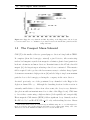
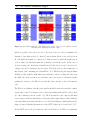
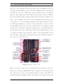
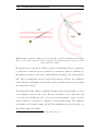
1
Development of Trigger and Control Systems for CMS J. A. Jones High Energy Physics Blackett Laboratory Imperial College London A thesis submitted for the degree of Doctor of Philosophy of the University of London and the Diploma of Imperial College December 2006 Abstract During the year of 2007, the Large Hadron Collider (LHC) and its four main detectors will begin operation with a view to answering the most pressing questions in particle physics. However before one can analyse the data produced to find the rare phenomena being looked for, both the detector and readout electronics must be thoroughly tested to ensure that the system will operate in a consistent way. The Compact Muon Solenoid (CMS) is one of the two general-purpose detectors at CERN. The tracking component of the design produces more data than any previous detector used in particle physics, with approximately ten million detector channels. The data from the detector is processed by the tracker Front End Driver (FED). The large data volume necessitated the development of a buffering and throttling system to prevent buffer overflow both on and off the detector. A critical component of this system is the APV emulator (APVe), which vetoes trigger decisions based on buffer status in the tracker. The commissioning of these components, along with a large part of the Timing, Trigger and Control (TTC) system is discussed, including the various modifications that were made to improve the robustness of the full system. Another key piece of the CMS electronics is the calorimeter trigger system, responsible for identifying ‘interesting’ physical events in a background of well-understood phenomena using calorimetric information. Calorimeter information is processed to identify various trigger objects by the Global Calorimeter Trigger (GCT). The first component of this system is the Source card, which has been developed to transfer data from the Regional Calorimeter Trigger (RCT) to the Leaf card, the processing engine of the GCT. The use of modern programmable logic with high speed optical links is discussed, emphasising its use for data concentration and the benefit it confers to the processing algorithms. Looking forward to Super-LHC, a possible addition to the CMS Level-1 trigger system is discussed, incorporating information from a new pixel detector with an alternative stacked geometry that allows the possibility of on-detector data rate reduction by means of a transverse momentum cut. A toy Monte Carlo was developed to study detector performance. Issues with high-speed reconstruction and the complications of on-detector data rate reduction are also discussed. 2 Acknowledgements To Geoff my supervisor, for letting me build things that other people wouldn’t have entrusted to me. Costas Foudas for getting me interested in High Energy Physics and for being a mentor. Mark Raymond, for being a genuinely great (and far too modest) person. Matthew Noy, for pushing me further than I could have gone on my own working on the I-ImaS project, teaching me to drink Guinness and for being a good friend. My family, for looking out for me when I was too tired to notice. Renata Longo and Christian Venanzi, for going far beyond the call of duty working with us on the first I-ImaS beam test. Freya Blekman, for giving me an idea of the practical side of hadronic physics. Jose Carlos Rasteiro Da Silva, Mike Matveev and Paul Padley for their advice on optical link design. Jan Troska for his help testing the Source card optical links and measuring the QPLL locking range. Magnus Hansen and Matt Stettler for being great colleagues to work with - I learned a lot from you guys. Andrew Rose, for knowing far too much about most things for a 1st year PhD student and being modest about it. Gregory Iles, who provided advice on the IDAQ design and helped get me started with FPGAs when I was first learning and for the time spent working on the CMS GCT. James Leaver - how you work so religiously I’ll never know. Davy Machin on the I-ImaS project - ni hao! Renato Turchetta, Jamie Crooks and Andrea Fant at Rutherford Appleton Laboratory for their insight and pub lunches working on the I-ImaS and HEPAPS sensors. Sarah Greenwood for doing a brilliant job on the IDAQ and GCT Source card PCB layouts, and for putting up with me when I changed my mind! Maria Khaleeq, Vera Kasey and Dave Price in the electronic workshop for their advice and help. Mark Pesaresi, for being quick with a joke when the mood got too serious. Everyone else in Imperial HEP for their help in whatever form it took. Kate Bishop for her incredible cooking! Seb Tallents for being around when things got too much, and for discussions about the finer points of the British political system (although you did all the talking!). Stephanie Wright for understanding that my PhD took up a lot of my time and not complaining (although you had every right to!). Paul Spicer at the Royal College of Music and Timothy Salter at the Ionian Singers for letting me sing - it took my mind off the thesis! Richard Hallam, Chris Rogers, William Panduro-Vazquez, Catherine Fry, Stuart Wakefield - it was fun being in your year. 3 Contents Abstract 1 Acknowledgements 2 Contents 3 List of Figures 8 List of Tables 16 Preface 17 Chapter 1. Introduction 17 1.1 Current Searches in Particle Physics 18 1.2 The Large Hadron Collider (LHC) 21 1.3 The Compact Muon Solenoid 26 1.3.1 The Silicon Tracker 27 1.3.2 The Electromagnetic Calorimeter 31 1.3.3 The Hadronic Calorimeter (HCAL) 32 Contents 1.4 4 1.3.4 The Muon Detectors 33 1.3.5 The CMS Trigger System 33 1.3.6 XDAQ 36 Programmable Logic Devices 37 1.4.1 History 37 1.4.2 The Complex Programmable Logic Device (CPLD) 38 1.4.3 The Field Programmable Gate Array (FPGA) 38 1.4.4 FPGA Clock Management 39 1.4.5 Input-Output Interfaces 40 1.4.6 Additional Features in Modern FPGAs 41 Chapter 2. Integration of the CMS Tracker Readout System 43 2.1 The CMS Tracker Readout System 43 2.2 The Tracker Front End Driver 47 2.3 Buffer Overflow in the CMS Tracker 48 2.3.1 The APV25 Readout Buffer 48 2.3.2 The APVe 49 2.3.3 Implementation of the APVe Firmware 50 2.3.4 The APVe Software Interface 51 2.4 Integration of the APVe 53 2.4.1 Integration with the Global Trigger 53 2.4.2 Online Recording of Trigger Statistics 54 Contents 2.5 2.4.3 Feedback Loop Latency 56 2.4.4 Implementation of the FED Deglitcher Module 57 Commissioning of the Tracker FED 59 2.5.1 Fake Event Generation 59 2.5.2 Test Setup 60 Chapter 3. 3.1 5 The Global Calorimeter Trigger 62 The Calorimeter Trigger Algorithms 62 3.1.1 Electron/Photon (e/γ) 63 3.1.2 Jets 63 3.1.3 Other triggers 65 3.2 The Global Calorimeter Trigger 65 3.3 The GCT Source Card Design 68 3.3.1 Development Challenges 72 3.3.2 Firmware Architecture 75 3.3.3 Software Architecture 82 3.4 Evaluation and Testing of the Source Card 84 3.4.1 RCT Emulator Data Capture 85 3.4.2 Integration with the RCT 89 3.4.3 Optical Links 91 3.4.4 QPLL Locking Range 94 3.4.5 Source Card Production Testing 94 Contents Chapter 4. 6 Super-LHC and the CMS Trigger 97 4.1 Implications for the CMS L1 Trigger 97 4.2 Tracker Contributions to Triggering 99 4.2.1 The Electron Algorithm 99 4.2.2 The τ -Jet Algorithm 4.3 4.4 4.5 4.6 4.7 100 Issues with the Implementation of a new Tracker 100 4.3.1 Tracker Occupancies and Data Rate 100 4.3.2 Limitations of the Current CMS Tracker 101 4.3.3 Reconstruction Combinatorials 102 Implementation of Stacked Tracking 106 4.4.1 Reconstruction 106 4.4.2 Probability of Hit-Pair Finding 109 Simulation Studies 110 4.5.1 Simulated Reconstruction Performance 112 4.5.2 Simulated Resolution 115 Double Stack Reconstruction 117 4.6.1 Reconstruction Method 118 4.6.2 Transverse Momentum Resolution 121 4.6.3 Projected Resolution 122 Reconstruction Implementation 124 4.7.1 124 Correlation Logic Implementation Contents 4.8 7 4.7.2 Data Processing Flow 125 4.7.3 Further Improvements 127 Summary Chapter 5. Appendix A. 128 Conclusions Development and Evaluation of the IDAQ A.1 Design of the Imperial DAQ (IDAQ) 129 131 131 A.1.1 Board Components 133 A.1.2 PCB Stackup and FPGA Decoupling 136 A.1.3 Upgrade Possibilities 138 A.2 Evaluation and Testing 138 A.3 Summary 139 Appendix B. VHDL Code Examples 140 B.1 CRC-32 Generator 140 B.2 The TTC SERIAL B Decoder 145 B.3 The FED Status Deglitcher 148 B.4 4-Phase Interlocked Strobe 150 B.5 Trigger Histogrammer 152 Glossary 154 References 160 8 List of Figures 1.1 The five second-order WW scattering diagrams in the Standard Model. Note that the two diagrams involving the Higgs boson act to cancel the divergences in the other three diagrams. 19 1.2 Latest results of searches for the Higgs boson. Taken from [1]. 20 1.3 Total pp collision cross-sections for varying collision energies [2]. The highest-energy points in this plot are from cosmic ray data. 22 1.4 Higgs production channels at the LHC. 24 1.5 Signal for mH =130GeV H→ γγ after 100fb−1 of data recorded. The Higgs signal is shown in red, background in yellow. Adapted from [3]. 1.6 25 Higgs discovery channels at CMS. Depending on the Higgs mass, various decays become favourable due to a combination of production rates for the intermediate particles and the background rates. 26 1.7 Diagram of the CMS detector. 27 1.8 Layout of a quarter of the CMS tracking detector. This image is mirrored along both axes to make the full detector layout. The interaction point is marked at z=0. 28 List of Figures 1.9 9 A single APV data frame with the passage of time indicated by the horizontal axis. A frame begins with a digital header including pipeline address information, followed by analogue voltage levels for each of the 128 APV channels in that bunch crossing. The end of the frame is indicated by another digital strobe. Taken from [4]. 30 1.10 Diagram of the CMS trigger/Data AcQuisition (DAQ) system. Data from the detector are first sent to the Level-1 trigger for processing and then selected events have the front-end detector data sent to the Higher Level Trigger for further processing. Status reports from the different subsystems allow debugging and throttling of the trigger systems to allow a sustainable trigger rate to be attained. 34 1.11 Diagram of the CMS L1 trigger. Most of the system is located in the underground cavern next to the detector to minimise latency. The only exception to this is the first part of the muon track finder, which is attached to the outside of the detector. 35 1.12 Diagram of a ROM LUT. The device is programmed with the equivalent output for every permutation of input to a particular logic circuit. 38 1.13 Diagram of a four-input FPGA LUT. The multiplexer selects between registered and unregistered modes of operation, allowing large combinatorial circuits to be produced. Alternatively registers can be used to create more pipelined designs. 39 2.1 Diagram of a CMS tracker partition. 44 2.2 Diagram of the CMS tracker FED. 48 2.3 Diagram of IDAQ connections for the APVe. 50 List of Figures 2.4 10 Theorised readout ‘dead-time’ for the CMS tracker [5]. This directly depends on the control loop size, which is related to the number of APV buffers than can be used before the APVe asserts BUSY. The solid line indicates the performance when using the ‘virtual’ APV emulation in the FPGA, whilst the dashed line represents the performance achieved when using the ‘real’ APV. 2.5 51 The main page of the APVe HyperDAQ interface, showing the basic settings and status information for one of the boards. 52 2.6 Test setup for integration of the APVe with the global trigger system. 53 2.7 Two examples of the APVe asserting ERROR when an orbit BC0 from the TCS-9U coincides with a L1 trigger. The magenta trace shows the BC0 strobe, the cyan trace represents L1As and the yellow trace represents a READY → ERROR transition. Note the missing BC0 when it coincides with a L1 trigger. 2.8 54 Results from a real-time histogram of the trigger distribution as measured by the APVe during testing, as viewed using the HyperDAQ interface. In this case the LTC was being used to generate a fake Poisson trigger distribution with a mean of 100kHz. 2.9 56 Measurements of a READY-WARN transition at the APVe FMM input connector. The purple trace represents the de-assertion of a READY state, whilst the green trace represents the assertion of a WARN state. 58 2.10 Data loss when throttling during a full FED test using 100kHz Poisson triggers (adapted from [6]). These measurements are compatible with those in [7]. 61 3.1 The calorimeter trigger e/γ algorithm [8]. 63 3.2 The calorimeter trigger jet algorithm [8]. 64 List of Figures 3.3 11 The GCT architecture. The half-barrel geometry of the detector is mirrored by the hardware in its symmetry from left to right. 67 3.4 Picture of a Source card. 69 3.5 Simplified schematic of data flow through a Source card during normal operation. RCT data are captured by the FPGA, multiplexed and fed into four serialisers. The entire board is driven by either a local test oscillator or LHC clock via the TTC input. A USB link provides a control interface for board settings. 71 3.6 The Source card clock system. 74 3.7 Schematic diagram of the Source card firmware. 75 3.8 Interlocking method for passing strobes between the TTC (40MHz) and RCT (80MHz) clock domains. When the rising edge of the TTC clock does not coincide with an edge of the RCT clock: (a), either edge can be used to transfer the strobe into the transmitter clock domain. However when coincidental with an edge either the rising or falling edge can be used (whichever is not coincidental with the TTC clock rising edge): (b). 78 3.9 Data pathway for the transmitter clock domain. 79 3.10 Data registering architecture for the receiver clock domain (adapted from [9]). 3.11 Software implementation for the Source card. 81 83 3.12 The RCT emulator card. It is designed to be mounted on an IDAQ. The ICs are TTL-ECL converters which take signals from the FPGA on the IDAQ. Next are the -5V bias resistors and two VHDCI (HD68) SCSI connectors. 85 3.13 Component interconnections for the RCT emulator-Source card test. A common clock from a TTCci is shared by the Source card and two RCT crates, making a synchronous test possible. Data from the JETSUM 5 output on each RCT crate is captured by the Source card. 86 List of Figures 12 3.14 Component interconnections for the RCT-Source card integration test. 89 3.15 Calibration of the RCT data capture window. The red region around the rising edge of the TTC/RCT clock represents the period of time during which the data lines are not stable. The green region represents stable data. In order to capture data efficiently, the rising edge of the Source card (SC) clock should be aligned with the middle of the valid data region. 90 3.16 Eye diagrams of high-speed signals from the Source card. 92 3.17 Test setup for measuring the effect of optical attenuation on the GCT links. 92 3.18 PRBS test interconnections between two Source cards. Each serial link on one board is connected to one of the serial links on the other board. 93 3.19 Final test setup for the GCT Source cards. Having qualified four Source cards for final use, the rest of the boards can be qualified using four routed receivers (one per card). This allows all of the tests to be carried out with little human intervention. 4.1 95 L1 single muon trigger rates for CMS [10]. Note the flattening of the L1 and L2 trigger curves where tracking information is not used. Only the additional information provided in the HLT at L2.5 and L3 can provide sufficient momentum resolution to control the trigger rate. 98 4.2 The HLT electron algorithm - taken from [11, 12]. 100 4.3 The HLT τ -jet algorithm [10]. 101 4.4 Simulated occupancy in the CMS tracker in SLHC. 102 4.5 Illustration of the principle of a search window for pixel seeding. 103 4.6 Track overlap in y-z plane (detector co-ordinates). Note the significant overlap of tracks between these two layers in the case of 1cm layer separation, which will hinder track reconstruction. 105 List of Figures 4.7 13 Average number of hit combinations per bunch crossing versus count r=10cm for varying pixel layer separations, with a pT cut of 1GeV. For this plot 100 minimum bias events were super-imposed for each bunch crossing. 4.8 Basic layout of a flat stacked tracker (not to scale). Left is a y-z view, right is an x-y view. 4.9 105 106 Illustration of the effect of the size of the luminous region on the overlap of the segments of the detector. 107 4.10 Mean cumulative count of the charged particles per collision versus their radius of curvature, counting from high to low pT . 100 super-imposed events per bunch crossing are used in this plot. The discontinuities seen at higher pT are the result of limited statistics. 108 4.11 Tangent-point reconstruction in detail. In a binary readout scheme, a pixel is simply active or inactive. There are things that can happen during correlation: (a) The track is always found in the search. (b) A lower-pT track may or may not be recorded depending on the impact point of the track on the sensor. (c) The pT is low and so the track will never pass a search. 109 4.12 Capture probabilities for particles with varying transverse momenta. The rφ pitch is 20µm. Inner sensor radius is 10cm. 110 4.13 Three stages of simulation: The tracks are constructed (light grey), hits are found (cyan) and those passing the geometrical pT cut are selected for readout (pink). The dark blue track is from a high-pT lepton. 4.14 Charge sharing model. 111 112 4.15 From left to right: Pure (a), impure (b) and incorrect (c) track reconstructions. 113 List of Figures 14 4.16 Illustration of the effect of charge sharing. In this case, if a search window of only one pixel in ±rφ is chosen, the track will be considered to have a higher pT than it does in reality, and some information about the cluster will be lost. 116 4.17 Azimuthal angular separation in radians for a given particle pT between the projected tangent of a track at its point of intersection with the stacked tracker and the point on the calorimeter which it hit. 117 4.18 Minimum and maximum pseudo-rapidities for a given pixel pair. This is referred to as the min-max range. A similar method is used to calculated the ∆φ resolution. 118 4.19 The stub resolution for a track extrapolated to the calorimeter. The values depend on both the separation between the two sensor layers and the position of the calorimeter hit. The values shown on the plot represent ∆η. 119 4.20 Reconstruction using the double-stack method. The left diagram shows the straight-line projection of the track in the rz plane, while the other diagram shows the curved projection of the track in the rφ plane. 120 4.21 The four stages of double-stack reconstruction. In addition to the three stages used in a single stack, once the data has been sent off-detector a correlation is made between stubs in the individual superlayers. 121 4.22 Transverse momentum measurement using the double-stack method. The black line represents the reconstruction transverse momentum cut, the ‘true’ points are from simulation and the red and green lines represent the largest possible error in reconstructed pT and therefore the worst-case momentum resolution. 123 List of Figures 15 4.23 Reconstructed angular resolution at the calorimeter-tracker interface plotted as a function of real transverse momentum. The black line represents the reconstruction transverse momentum cut, the ‘real’ points are from simulation and the red and green lines represent the largest possible ±∆φ variation and therefore the worst-case momentum resolution. Note the significantly improved resolution when compared to figure 4.17. 124 4.24 Projected ECAL resolution in η using the double-stack method. Note the significantly improved resolution when compared to figure 4.19. It should be borne in mind that a full simulation would include material effects, which would result in a ‘band’ for reconstruction resolution rather than a line. 125 4.25 Illustration of different stages of data processing both on and off-detector. The top half of this diagram represents on-detector electronics whilst the bottom half is off-detector. A.1 Block diagram of the IDAQ. 126 132 16 List of Tables 1.1 Examples of Level-1 triggers and their relation to their underlying physics channels. Taken from [8]. 1.2 Examples of various I/O standards and their supply voltages in Xilinx devices. 2.1 36 41 Latencies between various test points for a READY→WARN transition. The values are rounded to the nearest bunch crossing as this reflects the registered nature of the transmitted signals. 2.2 57 Skew measurements between the READY and WARN states on the FED and FMM, measured to the nearest 100ps. 58 3.1 Latency measurements between different test points in the Source card. 88 3.2 Contributions to skew on the GCT Source card. 91 4.1 Performance of a detector stack for sensors of lateral pitch 20x50µm2 (rφxz). 114 17 Chapter 1 Introduction “Who has seen the wind? Neither I nor you: But when the leaves hang trembling, The wind is passing through Who has seen the wind? Neither you nor I: But when the trees bow down their heads, The wind is passing by.” - Christina Rosetti The search for the Higgs boson or other even more elusive signs of new physics is like searching for something as ethereal yet omni-present as the wind. It is not surprising that modern physics is looking for something so difficult to find; every generation of particle physics experiment naturally has to look with a keener eye than the previous one. This necessitates an improvement in the ability to identify the significant features in a background of less significant events and record them on a very short timescale (µs-ms). Hence this ‘feature extraction’ must occur ‘online’, in customised hardware rather than in software on a computer. This thesis considers the many demands placed on modern hardware for these purposes, in both current and future particle physics applications. 1.1 1.1 Current Searches in Particle Physics 18 Current Searches in Particle Physics The vast majority of particle physicists are focused on the search for the Higgs boson [13, 14, 15, 16, 17, 18]. This is motivated by the fact that particle masses are otherwise not present in the mathematics of Quantum Field Theory (QFT). Furthermore, the W and Z bosons would be massless if the fundamental symmetry of the electroweak sector was not broken. This must be achieved in a way that is locally gauge invariant. The scalar Higgs field was introduced as an additional term in the Standard Model Lagrangian as a solution to both of these problems. In the form taken in the Standard Model it comprises a doublet of complex scalar fields, resulting in four degrees of freedom. Three of these degrees of freedom are used to assign mass to the W and Z bosons; the fourth degree of freedom results in the Higgs boson itself. The Higgs boson couples to all massive particles in the Standard Model, with the coupling strength related to the mass of the particle. In the case of the W and Z bosons this coupling can be derived directly from the Higgs mechanism. The masses of the fermions are introduced explicitly using the Yukawa couplings. The Higgs boson can also interact with the W and Z bosons directly, and in this way, (at least in the perturbative limit), it is responsible for cancelling the divergences found in WW scattering diagrams by providing a counterterm to the longitudinal component of the W boson (see figure 1.1), restoring gauge invariance while allowing the W to acquire mass. This is the key difference between using a Higgs model and introducing the W mass directly, which would not include these cancellation terms. Figures 1.2(a) and 1.2(b) are the latest predictions for the most likely mass of the Higgs boson. While its mass is not currently well known (if indeed the particle exists at all), the most likely mass can be inferred using measurements from the electroweak sector [1]. Indirect experimental bounds for the Higgs mass can be calculated from electroweak observables, which are related to couplings between the Higgs boson and other fundamental particles. The reason for this derives from radiative corrections to the W± and Z propagators, for which the dominant effects are the W + → b̄t → W + , W − → t̄b → W − , Z → t̄t → Z, Z → HZ → Z and 1.1 Current Searches in Particle Physics 19 Figure 1.1: The five second-order WW scattering diagrams in the Standard Model. Note that the two diagrams involving the Higgs boson act to cancel the divergences in the other three diagrams. W ± → HW ± → W ± processes. Hence, by accurate measurement of the W± , Z, t and b masses, one can infer the most likely Higgs mass. Initial estimates for the mass of the Higgs boson were calculated by the SLD experiment at SLAC [19] and the four LEP experiments [20]. As both experiments involved collisions between electrons and positrons they allowed both indirect measurements based on precision measurements of the Z and W boson mass and that of the b quark, and direct searches by looking for a resonance at the Higgs mass. Direct searches [21] were carried out at LEP by studying the Higgsstrahlung process e+ e− → HZ and the following decay modes: • H → bb̄, Z → q q̄ • H → bb̄, Z → ν ν̄ • H → bb̄, Z → e+ e− , µ+ µ− • H → τ + τ − , Z → q q̄ and H → q q̄, Z → τ + τ − 1.1 Current Searches in Particle Physics 20 The results of these searches, marked by the yellow region in figure 1.2(b), exclude the possibility of a Standard Model Higgs mass less than 114.4GeV (95% confidence level). (a) 68% confidence level region given the (b) χ2 plot of mH using the Tevatron and current best measurements of mW and the results of direct LEP searches. mt . Figure 1.2: Latest results of searches for the Higgs boson. Taken from [1]. Proton colliders such as the pp̄ Tevatron accelerator [22] have improved statistical limits on estimates of a Higgs mass greater than 114.4GeV. In particular measurements of the mass of the top quark have been significantly improved upon (currently 170.9±1.8GeV [23]), and therefore predictions of the most likely Higgs mass have also improved. However due to the high levels of background particles in proton colliders, it is very difficult to detect a Higgs boson directly. While the Higgs is an elegant solution to the existence of symmetry breaking in the electroweak sector, as stated previously it (or something else) is also necessary to balance higher-order corrections to WW scattering (i.e. W W → X → W W ), which theoretical arguments otherwise predict will become divergent at an energy scale of approximately 1TeV (the so-called ‘unitarity problem’ [24]). If the Higgs boson does not exist, it will be necessary to study WW scattering in this energy range to understand what alternative mechanism is at work to prevent instabilities in the theory. 1.2 The Large Hadron Collider (LHC) 21 Even the Standard Model Higgs presents additional complications [25]; for example, the calculation of the Higgs mass directly from theory suffers higher-order quadratic and logarithmic divergences which occur as a result of radiative corrections to the Higgs mass. While the logarithmic divergences can be treated by using renormalisation, the quadratic divergences cannot. This is known as the naturalness problem as the only way to manage it within the limits of the Standard model is to fine-tune all the constants in the theory to an extremely precise degree. One possible solution to this problem is the introduction of SUperSYmmetry (SUSY) [26], in which every fermionic particle in the Standard Model would have a bosonic partner and vice versa. This cancels the quadratic radiative corrections to the Higgs mass through additional terms occuring due to couplings between the Higgs and several additional supersymmetric particles. While this stabilises the Higgs field, it leads to not only a plethora of new particle types (squarks, gluinos and neutralinos to name a few), none of which have yet been observed, but also to at least five different types of Higgs boson in the Minimal SuperSymmetric Model (MSSM). Furthermore it requires the measurement and tuning of 105 constants in addition to those already found in the Standard Model. A new higher-energy particle beam should give some indication of whether SUSY exists in the real world, providing coverage of at least part of the SUSY parameter space. There are many other models and potentially interesting physics phenomena that can be studied using energy scales at the TeV level and beyond. These include precision measurements of Charge-Parity (CP) violation, related to the asymmetry between the amount of matter and anti-matter in the universe [27]. In any case the motivation for a high-energy collider is clear. 1.2 The Large Hadron Collider (LHC) The LHC [28] is the planned proton-proton collider based at CERN, operating at a centre-of-mass energy of 14TeV, collision rate of 40MHz and a nominal luminosity of 1034 cm−2 s−1 . As a proton collider, it is a ‘statistics engine’, designed to produce large numbers of Deep Inelastic Scattering (DIS) collisions during every bunch crossing 1.2 The Large Hadron Collider (LHC) 22 (BX). This is expected to permit the discovery of new physics up to an energy of 1TeV, physics above this energy being more difficult to study due to limited statistics (although sometimes the signatures can be unmissable [29]). The event rate at the LHC depends on the large cross-section for pp inelastic scattering as shown in figure 1.3. Figure 1.3: Total pp collision cross-sections for varying collision energies [2]. The highest-energy points in this plot are from cosmic ray data. At an energy scale of 14TeV the total cross-section is estimated from cosmic ray data to be 100mb, of which 30mb is expected to be elastic and therefore not as relevant to the experiments. The rate at which an event occurs is defined as the product of the cross-section and the luminosity of the accelerator: N = Lσ (1.1) where N is the event rate per second, L is the luminosity in cm−2 s−1 and σ is the event cross-section in cm2 . Therefore a 70mb (70 ∗ 10−27 cm2 ) inelastic scattering cross-section at a luminosity of 1034 cm−2 s−1 results in an event rate of 7x10⁸ s−1 . As the bunch crossing rate is 40MHz and bearing in mind that during normal operation at the LHC not all bunches are filled (only 2808/3564), the number of events per bunch crossing can be calculated as: Rate = 7 ∗ 108 ∗ 25 ∗ 10−9 ∗ 2808/3564≃22 (1.2) 1.2 The Large Hadron Collider (LHC) 23 As the energy scale and raw data rate aimed for at the LHC are much higher than in previous experiments, there are a number of resulting detector implementation issues which can be summarised as follows: • Intensity - The intended design luminosity is 1034 cm−2 s−1 . This leads to problems both in terms of radiation damage and pileup effects, in which the energy deposited by particles generated by the previous proton bunch crossing, and also the particles themselves, are still present in the detector. This problem is exacerbated by the fact that there are an average of 22 proton-proton collisions per bunch crossing. • Crossing Rate - In order to achieve the desired instantaneous luminosity the bunch crossings occur once every 25ns, which places strict requirements on the speed of the readout electronics and the charge collection time of the detectors. • Radiation Damage - Detectors in the LHC suffer a variety of types of damage from high energy protons, neutrons and pions and also ionisation effects from photons and charged particles. The dose is highest in the forward regions and the inner detector; for example it can reach 30MRad and 1015 neq /cm2∗ in the CMS pixel detector [30]. The issues described above are also inter-related (for example a change in bunch crossing rate is directly related to a change in the luminosity). In any case these criteria require the design of detectors and readout electronics that are capable of operating for ten years in this harsh environment, which must withstand both longterm damage and Single Event Upsets (SEUs) [31], where a charged particle passing through the readout electronics changes the state of a single bit in a digital logic circuit or memory (typically triple-redundant logic circuits with a majority sum rule [32] are implemented to reduce the probability of this occurring). The detectors have to be everything at the same time - fast, radiation-hard and low-noise. This isn’t ∗ neq /cm2 is the neutron equivalent particle flux that pass through every square centimetre of the material. 100Rad=1Gy. 1.2 The Large Hadron Collider (LHC) 24 currently possible so trade-offs are made in the design of each detector to improve the quality of a particular measurement. The two smaller detectors at the LHC are focused on particular physics areas: CPviolation in the B sector (LHCb) [33] and heavy ion physics (ALICE) [34]. The other two larger detectors (CMS [35] and ATLAS [36]) are designed with general-purpose studies in mind and the search for the Higgs boson in particular. Figure 1.4: Higgs production channels at the LHC. There are four major production channels for the Higgs at LHC (see figure 1.4), each of which is preferred at different energy scales and for different reasons: gg fusion, tt̄ fusion, W/Z fusion and W/Z bremsstrahlung. The reason that these reactions dominate is due to the Yukawa and Higgs couplings in the Standard Model - the strength of the coupling of the Higgs to a particle determines its mass, which also means that heavier particles have greater cross-sections for Higgs production. Although gg fusion is by far the dominant production channel, it suffers background from quark annihilation and gluon box diagrams; therefore it is most useful when combined with a distinct decay channel. A key decay channel for CMS at lower Higgs masses is H→ γγ, which requires excellent calorimetry in order to identify the signal over the background (see figure 1.5). It is worth noting also that while these 1.2 The Large Hadron Collider (LHC) 25 are the dominant production channels for the Higgs, the production cross-sections are all at least nine orders of magnitude smaller than the total proton cross-section. Therefore only one in a billion events produced at the LHC are likely to be Higgs events. Figure 1.5: Signal for mH =130GeV H→ γγ after 100fb−1 of data recorded. The Higgs signal is shown in red, background in yellow. Adapted from [3]. H→τ τ can also be used when searching for smaller Higgs masses. For greater mH , H→ZZ→l+ l− l+ l− can also be used, as well as H→W W/ZZ→jjl+ l− . If the alternative production channel W/Z fusion is considered, it provides the additional benefit of a di-jet signature with a rapidity gap between them (due to the lack of colour transfer between the two quarks emitting the W bosons); this acts as a useful filter for the event. A summary of typical decay modes under study versus the Higgs mass is shown in figure 1.6. From these various signatures it is clear that in order to stand the best chance of finding the Higgs (and also studying other interesting channels involving heavy particles), we need very efficient tagging of particles such as b and t quarks as well as µ and τ leptons. We also require excellent calorimetry to detect electrons and photons. 1.3 The Compact Muon Solenoid 26 Figure 1.6: Higgs discovery channels at CMS. Depending on the Higgs mass, various decays become favourable due to a combination of production rates for the intermediate particles and the background rates. 1.3 The Compact Muon Solenoid CMS [37] is the smaller of the two general-purpose detectors being built at CERN. It comprises (from the beam pipe outward) a pixel detector, silicon microstrip tracker, lead tungstate crystal electromagnetic calorimeter, plastic-brass/quartz-iron hadronic calorimeter and muon detectors. Its main feature is the 4 Tesla solenoidal magnet [38], the largest superconducting solenoid ever constructed. This massive field is required both to produce the lever-arm necessary to calculate charged particle transverse momenta to high precision† [24] and also helps to trap low-momentum particles close to the beam pipe, reducing the occupancy in the outer detector. As stated previously, one of the prominent decay channels for the Higgs is the di-photon channel H→ γγ. Although the branching fraction for this reaction is extremely small relative to those from other events, the decay is very distinctive (two photons with an invariant mass close to that of the Higgs boson). CMS aims to detect these events using a high-resolution (both spatially and energetically) Electromagnetic CALorimeter (ECAL). Other significant decay channels, such as H→ZZ→l+ l− l+ l− and H→W W/ZZ→ννl+ l− rely on the tracking detectors. Muons † This measurement is made in a different way in ATLAS, using air-core toroidal magnets for muon spectrometry and a weaker magnetic field with no iron for flux return. Many of the other differences between the ATLAS and CMS detectors evolved from this choice. 1.3 The Compact Muon Solenoid 27 Figure 1.7: Diagram of the CMS detector. produced by these decays are relatively easy to identify because they travel practically unhindered through the detector. 1.3.1 The Silicon Tracker The CMS tracker [39, 40] (see figure 1.8) is an all-silicon detector comprising ten layers of microstrip sensors and three layers of pixellated sensor in the barrel. It is 5.4m long and has a diameter of 2.4m, and is subdivided into five main parts: The Tracker Outer Barrel (TOB), Tracker Inner Barrel (TIB), Tracker Inner Disks (TID), Tracker End Caps (TEC) and the pixels. The pixel detector has to cope with some of the highest fluences in CMS where the dose is 3.2x10¹⁵ neq cm−2 at 4cm radius from the beam pipe over the lifetime of the experiment. It must be situated as close to the interaction region as possible in order to tag relatively long-lived particles such as bottom and charmed hadrons and the τ , and to identify light quark and gluon jets. The microstrip tracker provides the necessary lever arm for accurate momentum measurements and improves the precision of vertex measurements [41]. The entire detector is operated at low temperature (minus ten degrees Centigrade) to minimise the effects of radiation damage. 1.3 The Compact Muon Solenoid 28 Figure 1.8: Layout of a quarter of the CMS tracking detector. This image is mirrored along both axes to make the full detector layout. The interaction point is marked at z=0. The pixel detector is a hybrid design combining a silicon sensor with pixel pitch 120x150µm2 (rφxz) and a series of bump-bonded ReadOut Chips (ROCs) [42]. The sensors and readout Application-Specific Integrated Circuits (ASICs) of the design were kept separate in order to provide a large depletion region and fast charge collection that will have a usable signal after very heavy irradiation, which in turn requires a large external bias voltage to be applied (up to 600 volts). The sensing element contains a set of n-on-n diodes and a contact pad for each bump bond. The readout chip contains electronics for a high-speed token-ring readout system, analogue readout of the pixels and digitisation of the analogue values at the periphery of the ROC. In order to optimise the resolution of the pixel detector in both the rφ and z directions, each module in the pixel end disks is rotated to take advantage of electron Lorentz drift in the sensor layer due to the 4T magnetic field. Analogue interpolation between the strips is also used to maximise resolution. The resolution of the pixel detector is anticipated to be approximately 10µm in rφ and 15-20µm in z [43]. Unlike the binary tracker used in ATLAS, the CMS microstrip tracker is an almost exclusively analogue design with approximately 10 million detector channels. It uses p+ -in-n microstrip sensors of pitches from 80µm upwards and either 512 or 768 strips per sensor, layered in an overlapping fashion to provide detector hermeticity. Some sensors are also placed back-to-back rotated relative to each other by approximately 1.3 The Compact Muon Solenoid 29 100mrad, providing two-dimensional hit detection in the outer tracker. Signals from each set of 128 microstrips are sampled into an analogue pipeline using an APV (Analogue Pipeline Voltage) [44, 45, 46] readout chip that is capacitively-coupled to the sensor. Each APV25 ASIC has been manufactured using a 0.25µm CMOS process [47], using enclosed gate technology in order to mitigate the effects of long term radiation damage in the detector environment. Each of the 128 readout channels in the APV25 has its own front-end preamplifier circuit followed by a CR-RC filter which shapes the charge pulse from the sensor to have a characteristic time constant of 50ns. The signal voltage is sampled at 25ns intervals into a 192-cell-deep analogue buffer of switched capacitors. The system has a response of 100mV/MIP (Minimum Ionising Particle‡ ) and a non-linearity of less than 2% over a 5 MIP range. The total power consumption is approximately 2.3mW/channel. The chip has two fundamental modes of operation. In peak mode (used at low luminosity), only the peak of the pulse shape is sampled into the APV25 pipeline and sent off-detector when a L1A (Level-1 Accept) is received from the trigger system. At higher luminosity, where pileup in a single channel is more likely, deconvolution mode is used [48, 49, 50, 51]; this involves sampling the pulse shape before the charge peak, at the peak and after, and using an Analogue Pulse Shape Processor (APSP) circuit to reconstruct the original charge peak at each bunch crossing. This does however contribute to a small increase in overall noise; more specifically, when operating in peak mode the series noise is reduced relative to deconvolution mode because only a single sample is used to create the resultant signal, however the signal is more prone to noise from pileup. Conversely in deconvolution mode the pileup noise is reduced by the use of three samples but the series noise is increased. After this the analogue signals are converted into the optical domain and time-division multiplexed in order to reduce the cabling requirements. An example of a single APV25 readout frame is shown in figure 1.3.1. These data are carried out of the detector by approximately 45,000 optical fibres. In the case of the microstrip tracker, zero-suppression is not performed until data reaches the ‡ A MIP is defined as a particle possessing a kinetic energy that deposits the minimum amount of energy possible in the sensitive region of a detector, and therefore defines the signal-to-noise ratio requirement for the sensor. 1.3 The Compact Muon Solenoid 30 Figure 1.9: A single APV data frame with the passage of time indicated by the horizontal axis. A frame begins with a digital header including pipeline address information, followed by analogue voltage levels for each of the 128 APV channels in that bunch crossing. The end of the frame is indicated by another digital strobe. Taken from [4]. front-end electronics of the tracker Front End Driver (FED). This is the major disadvantage of using an analogue system. It does however provide several benefits: • Reduced power consumption - Digitisation consumes power, and fast digitisation even more. This leads to requirements for greater power densities in the tracker and would also have resulted in the dissipation of additional heat. • Greater effective information - Interpolation of the charge distribution across several microstrips can improve the resolution beyond the pitch of the sensors themselves. • Immunity to noise - If pedestal subtraction is performed after readout, noise immunity can be improved upon. For example, one can isolate common mode noise and interference from external sources such as fluctuations in the detector ground level. Furthermore the use of an analogue system avoids the use of discriminator thresholds in the detector electronics, which can potentially cause a high ‘fake hit’ rate and would require constant monitoring and calibration. • Performance Monitoring - As the analogue pulse shape is monitored offdetector, any degradation of sensor or electronic performance can be monitored throughout the operation of the experiment. 1.3 The Compact Muon Solenoid 31 As the signals from the tracker are not digitised until they reach the FED, data from the tracker is unavailable for a 7µs readout period. Therefore it is unable to contribute to the first stage of triggering in CMS. This may be of critical importance for Super-LHC (SLHC), as discussed in chapter 4. 1.3.2 The Electromagnetic Calorimeter The ECAL [3] is a very compact homogeneous scintillating crystal calorimeter designed for precision measurements of electron and photon energies (0.5%@50GeV). For high-energy particles, electromagnetic calorimeters rely on the use of materials that promote two processes: electron (and positron) Bremsstrahlung emission of photons, and the conversion of photons into electron-positron pairs (called ‘pairproduction’). These processes are characterised by the radiation length, X0 , which is the distance over which and electron (or positron) loses, on average 1 − 1 e of its 7 energy. The probability of a pair conversion over a single radiation length is e− 9 . As one of these two processes naturally gives rise to the other, a cascade of particles is produced, ultimately resulting in a multitude of low-energy photons that can be detected and used to measure the energy of the initial particle. In order to achieve the required performance in the limited space available in CMS, lead tungstate was chosen as the active material for its short radiation length (approximately 0.9 cm) and high radiation tolerance. Each crystal has a front face 2.2x2.3cm2 in the barrel section (approximately 0.0175 square in ∆ηx∆φ). As the active material has a relatively low light yield, the signal from the light collected must be amplified. This is achieved using Avalanche PhotoDiodes (APDs) in the barrel (two per crystal) and Vacuum PhotoTriodes (VPTs) in the end caps where the radiation dose is greater. The signals from the ECAL are digitised on the detector, then stored for readout upon the reception of a readout trigger. In addition to this trigger primitives are generated on-detector using 5x5 crystal ‘trigger towers’ and forwarded to the calorimeter trigger off-detector (see chapter 3). 1.3 1.3.3 The Compact Muon Solenoid 32 The Hadronic Calorimeter (HCAL) Surrounding the ECAL is the HCAL [52] that is responsible for energy measurements of hadrons and their products (i.e. jets) with an energy resolution (when combined √ with the ECAL) of σE /E = 120%/ E ⊕ 6.9% [43], where E is measured in GeV. Hadronic calorimeters rely on nuclear interactions which result in both hadronic and electromagnetic showers. Interactions are defined in terms of the nuclear interaction length λ, which is greater for more dense materials. As the probability of a nuclear interaction is small but the energy deposited in the calorimeter is large, there are significant fluctuations in the measured energy in hadronic calorimeter showers, lowering the overall energy resolution of the detector. Pions play a key role in shower development in a hadronic calorimeter, as they are the lowest-energy products of nuclear interactions. Neutral pions from the proton collisions convert close to the interaction point in CMS to produce two photons which are subsequently absorbed by the electromagnetic calorimeter. Therefore the photons from these particles do not reach the hadronic calorimeter. However the nuclear interactions in the HCAL itself produce neutral and charged pions. The charged pions can further interact with the detector to produce more neutral pions, which then decay to produce photons that are detected in the HCAL. This leads to multiple large depositions of energy throughout the HCAL, which are then combined to reconstruct the energy of the incoming particle(s). The measurement of the energy by the detection of photons is achieved in the barrel and endcap regions using a sampling calorimeter, with brass absorbers and plastic scintillators, coupled to wavelength-shifting fibres and Hybrid PhotoDiode (HPD) sensors. In the very forward end cap region (HF), quartz fibres emitting Cerenkov light are used instead of plastic and embedded into iron due to their greater radiation tolerance. They are coupled to phototubes, which are faster than the HPDs used in the central region of the detector. Total HCAL detector coverage reaches |η| = 5. 1.3 The Compact Muon Solenoid 1.3.4 The Muon Detectors 33 CMS contains three different types of muon detector [53, 54]. The barrel contains Drift Tube (DT) chambers for precision track measurement, whilst the end caps use Cathode Strip Chambers (CSCs). In addition, Resistive Plate Chambers (RPCs) are used in both parts of the system for triggering detectors; the reason being that while they have poorer spatial resolution than the CSCs and DTs, they are capable of resolving individual bunch crossings in time and are therefore needed for Level-1 triggering. The spatial resolution of the muon detectors is between 50 and 200µm, while the standalone momentum resolution is at most 15% for a particle with 10GeV pT , and 40% at 1TeV. 1.3.5 The CMS Trigger System As the LHC is designed to operate at a very high event rate, there is neither the space nor detector readout bandwidth available to store all of the data produced. The readout rate is particularly limited by data storage space. Each event in CMS produces approximately 1MB of processed data and the total data volume produced by the CMS detector is several TB per second. The peak storage rate for CMS is approximately 1TB per day (100Hz), and therefore the data volume must be reduced by a factor of 400,000 before writing to disk. This necessitates the use of a ‘trigger’ system to pre-process a coarse-grained subset of the data. It is a common misconception that a trigger identifies ‘interesting’ events in the background and select them for further processing. This would by definition imply that one already knew what to look for; in fact the purpose of a trigger is to discard data that are understood with our current physical understanding and retain data relating to events that cannot be immediately identified. Of course at the same time one must ensure that the trigger has the capability to distinguish signatures of possible new physics and store them for further study, such as the anticipated Higgs boson. Essentially in CMS this reduces to a ‘cut’ on the transverse energy, 1.3 The Compact Muon Solenoid 34 missing transverse energy and types of particle detected. In doing this one is placing as few constraints as possible on the physics available to the end-user (ignoring low energy physics for which the LHC was clearly not designed). This is often described as ‘inclusive triggering’ and is particularly important for the first trigger stage. In addition to the requirement of efficient event selection, the trigger must also operate with minimal deadtime (a period after a trigger during which data cannot be taken), allowing one to maintain a high efficiency for the recording of useful events. This is achieved using buffers in the detector readout combined with a fast, efficient trigger processor. Figure 1.10: Diagram of the CMS trigger/Data AcQuisition (DAQ) system. Data from the detector are first sent to the Level-1 trigger for processing and then selected events have the frontend detector data sent to the Higher Level Trigger for further processing. Status reports from the different subsystems allow debugging and throttling of the trigger systems to allow a sustainable trigger rate to be attained. As shown in figure 1.10, the CMS trigger comprises two stages of event selection [8, 55, 10]. The Level-1 (L1) trigger [56] is primarily a Field-Programmable Gate Array (FPGA) and ASIC-based processing system in order to handle the enormous data volume from the detector and provide a trigger decision in a very short (and guaranteed) time period of 128 BX or 3.2µs§ . The goal of the system is to reduce the data volume by an average factor of 400 (i.e. to 100kHz). The Higher Level Trigger (HLT) reduces the rate by a further factor of 1,000 and is dominated by the use of PCs using a multi-stage iterative approach to reconstruction § There is in fact some margin in this requirement; the limiting factor in the trigger latency is the size of the tracker APV25 pipeline, which was originally 128 BX but increased to an effective latency of 160 BX in the final revision of the ASIC. 1.3 The Compact Muon Solenoid 35 with a limiting cut-off in allowed processing time. At this level basic tracker information is used, and initial selection based on possible underlying physics events is made. The data produced at this level of filtering is then recorded to disk at approximately 100Hz. Figure 1.11: Diagram of the CMS L1 trigger. Most of the system is located in the underground cavern next to the detector to minimise latency. The only exception to this is the first part of the muon track finder, which is attached to the outside of the detector. From figure 1.11 it can be seen that processing at L1 only uses data from the calorimeters (ECAL and HCAL) and tracks from the muon systems [57]. In the case of the muon trigger this simply involves creating a list of all the tracks detected in a bunch crossing, sorted by their transverse momentum. The top four candidates are then forwarded to the Global Trigger (GT). The calorimeter trigger objects are more complicated, and fundamentally comprise two types of trigger object, reflecting the two fundamental types of energy deposition in the calorimeter. The first of these are electron/photon candidates mostly detected by the ECAL, which are relatively spatially compact objects. The second type are jets from QCD events that shower in the detector, which produce a broader energy deposition pattern, mostly in the HCAL. The highest-ranked candidates of these types of deposition are again forwarded to the GT. The details of the calorimeter trigger are discussed in chapter 3. 1.3 The Compact Muon Solenoid 36 The GT combines candidates from these two systems and uses them to make a decision on whether to read out a particular event from the detector. The trigger depends on the object being sought, but generally involves simple criteria such as a single muon with a transverse momentum greater than a certain threshold. Composite objects such as two τ jets combined with two forward jets can also be used for triggering, although the types of trigger object should be kept as simple as possible in order to avoid creating bias in the recorded data. Some examples of triggers and their relation to underlying physics are shown in table 1.1. Physics Channel H→ γγ H→τ τ H→W W/ZZ→jjl+ l− H→W W/ZZ→ννl+ l− H→ZZ→l+ l− l+ l− Level-1 Trigger 2 electrons 2 τ jets 2 jets + (2 electrons OR 2 muons) Emissing + (2 electrons OR 2 muons) T 2 electrons OR 2 muons OR (electron + muon) Table 1.1: Examples of Level-1 triggers and their relation to their underlying physics channels. Taken from [8]. Tracker and pixel information is not currently used at this stage, simply because data from these detectors is not believed to be necessary for triggering under typical LHC conditions. Even if this belief were to change in the future, the current tracker could not support a full trigger system, due to the incredibly large data volume produced (far greater than that of all of the other detectors in CMS combined) and the choice of analogue optical link technology [58, 59] and off-detector zerosuppression [60, 61]¶ . 1.3.6 XDAQ In order to facilitate the efficient control of CMS, it is necessary to configure and monitor the myriad pieces of hardware in the system with a large degree of automation and across several different communication media. This is achieved using the Cross-platform DAQ (XDAQ) software package [62], which operates on a standard PC configured with CERN Scientific Linux [63]. ¶ It should be noted that there are strong motivations for this to change in the future (see chapter 4). 1.4 Programmable Logic Devices 37 The basic concept is to provide a platform-independent environment (called an executive) into which modules representing interfaces to different pieces of hardware in CMS are loaded. All of these modules are developed as libraries which contain C++ classes derived from a standard XDAQ template. Standard network protocols for message passing and data transfer are provided, including Simple Object Access Protocol (SOAP) and Intelligent Input/Output (I2 O) over TCP/IP, simplifying the development process. This allows the developer to focus on providing an application layer that exposes the functionality provided by the hardware. In addition to this, the latest version of XDAQ also provides generic Finite State Machine (FSM) functionality, allowing the CMS detector and DAQ to be globally configured, enabled and disabled from a single point of control. It also provides a web interface (called HyperDAQ) which allows control and monitoring of the hardware from a browser. 1.4 Programmable Logic Devices The design of the trigger and readout systems in all four of the primary experiments at the LHC would probably have been very different were it not for the astonishing rate of development of modern programmable logic. It has provided the facility for change in the function of the electronics, even after the underlying hardware has been manufactured, while significantly reducing development time. Simultaneously the rapid reduction in cost per equivalent logic gate and rapid increase in the capacity of these devices has allowed for extremely complex and fast processing to be developed at relatively low cost. 1.4.1 History Modern programmable logic comes in many guises. The two most common types are Field Programmable Gate Arrays (FPGAs) and Complex Programmable Logic Devices (CPLDs). The concept behind these devices evolved from the one-timeprogrammable Read Only Memory (ROM) in the 1960s (see figure 1.12). It was 1.4 Programmable Logic Devices 38 realised that the address table of such a device can be treated as a set of logic inputs, whilst the data bus can be treated as the output. As such, it can behave as any form of logic circuit possible using the same number of inputs as address pins, and the same number of outputs as data pins, the design complexity being limited only by the size of the device. This is often known as a Look-Up Table (LUT). Figure 1.12: Diagram of a ROM LUT. The device is programmed with the equivalent output for every permutation of input to a particular logic circuit. One limitation of this device lies in its inability to effect feedback internally, which is needed in particular for the development of state machines and algorithms that utilise hysteresis. As a result, devices evolved that combined the logic flexibility of the ROM with registering capabilities. 1.4.2 The Complex Programmable Logic Device (CPLD) The CPLD is one of the two major variants of programmable logic device currently available. Its main feature is the use of basic processing elements such as product terms and simplified routing networks, that provide basic processing and limited feedback, but maintain stable timing of the logic signals inside the device. They tend to be relatively small in equivalent-gate terms and tend to be used for routing, housekeeping or extending the capabilities of other devices such as microcontrollers. 1.4.3 The Field Programmable Gate Array (FPGA) The Field Programmable Gate Array is literally what its name implies - an extremely dense array of gates (or in fact the LUTs that often comprise the basic building 1.4 Programmable Logic Devices 39 blocks of most of these devices), combined with outputs that can either be configured as latches or clocked registers. This combination allows the creation of very large and complex designsk . A typical LUT in an SRAM-based FPGA (see figure 1.13) has four inputs, although modern devices can contain six or seven to improve performance [64, 65]. Figure 1.13: Diagram of a four-input FPGA LUT. The multiplexer selects between registered and unregistered modes of operation, allowing large combinatorial circuits to be produced. Alternatively registers can be used to create more pipelined designs. While FPGAs have a far greater logic capacity than CPLDs, their capacity comes at a price; as a result of the increased density and processing capabilities, the signal routing becomes intimately dependent on the way a design is implemented, the logic placement in the device and even on which pin of the device is connected to each external signal. This is often called the timing closure problem [66] and is becoming increasingly important as FPGAs grow in size, and designs become more complex. Various techniques are now being adopted for logic synthesis in FPGAs, such as physical synthesis [67], methods more commonly found in the world of ASIC design. Modern FPGAs come in several forms, the key distinction between them being whether their configuration is volatile (i.e. they lose their configuration at poweroff) such as SRAM FPGAs or non-volatile (antifuse, FLASH, etc.). The hardware described in this thesis uses SRAM-based FPGAs, and in particular those produced by XilinxT M [68]. 1.4.4 FPGA Clock Management Modern FPGAs contain much more than just LUTs, registers and a routing matrix. Some of the components that are required to design a programmable logic circuit are k Limited by logic and routing resources, and propagation delay through the circuit. 1.4 Programmable Logic Devices 40 not digital at all; one important example of this is the clock management system. Each type of FPGA has its own approach to dealing with clock management, but the principle is essentially the same. For a logic circuit to operate properly in an FPGA, the clock must reach every register in the design approximately simultaneously, and all signals must propagate to their destinations within that clock cycle. This defines the maximum speed at which a design can operate, which is directly related to the amount of data that can be processed. In order to ensure that the signal reaches all parts of the FPGA simultaneously, several dedicated ‘clock trees’ are available for the sole purpose of routing clock signals through the device with minimal skew. The clock for an FPGA must be provided by an external source, typically a dedicated oscillator which generates the frequency required for a given logic design. However one must also deal with possible design changes or a requirement for several clocks that operate at multiples of the basic oscillator frequency, possibly with a phase offset between them. This necessitates the synthesis of additional clocks in the FPGA. In Xilinx devices this is achieved using a combination of Digital Clock Managers (DCMs), Delay Locked Loops (DLLs) and Phase Locked Loops (PLLs). The number and type provided by these devices vary, but typically they are capable of producing several synthesised clocks with frequencies that are fractional multiples of the original frequency and with controlled phase offsets between them. These components can also be cascaded to produce more complex clock systems. In complex systems, the design of the clock tree is often at the heart of the design. This is particularly true in the Global Calorimeter Trigger Source card (see chapter 3). 1.4.5 Input-Output Interfaces Another fundamental part of an FPGA is the I/O interface. For an FPGA to be truly flexible, one must be able to reconfigure not only the internal behaviour of the logic, but also the type of electrical signal either received by or driven by the device. This is a far more difficult problem than the reconfiguration of the logic 1.4 Programmable Logic Devices 41 itself, as there are many electrical standards to be interfaced to, often requiring different supply voltages. For this reason the I/O on modern FPGAs is ‘banked’ or divided into regions, each of which can be provided with different supply voltages for different signal standards. In addition to the supply voltage there is also sometimes a reference voltage that defines the crossover point between a binary ‘1’ signal and a binary ‘0’. Some examples of signal standards, their voltages and typical uses are shown in table 1.2. Standard VSU P P LY (V olts) VREF EREN CE (V olts) LVCMOS 1.5/2.5/3.3 N/A LVTTL 3.3 N/A LVDS 2.5/3.3 N/A SSTL 2.5 1.25 HSTL 1.8 0.9 Use Low-Voltage CMOS Low-Voltage TTL High-speed/low-noise DDR memory QDR memory Table 1.2: Examples of various I/O standards and their supply voltages in Xilinx devices. These are just a few examples, but what is clear is that the I/O supply voltages limit the ultimate flexibility of the device, as external components may have to be connected to the FPGA through translation buffers unless a common signal standard can be found. In addition to the signal standards themselves, the latest devices provide controlled signal delays on both incoming and outgoing signals. This can be used to compensate for variations in signal propagation time outside the FPGA when signals are driven by a common clock. 1.4.6 Additional Features in Modern FPGAs As well as the more basic components described above, the latest generations of FPGAs have small ASIC-like components embedded in them to provide specific functions at high speed. Some examples include integrated processor cores [69] and multipliers or DSP blocks [70]. These can be extremely useful in particular applications such as TCP/IP packet switching or algorithmic processing. The components of particular use in particle physics are the integrated SERDES (SERialiserDESerialiser) devices, also known as Multi-Gigabit Transceivers (MGTs). They are used 1.4 Programmable Logic Devices 42 extensively in CMS and in particular in the Global Calorimeter Trigger, where they provide both data concentration, and also confer a degree of noise immunity. 2 Integration of the CMS Tracker Readout System 43 Chapter 2 Integration of the CMS Tracker Readout System ”In theory, there is no difference between theory and practice. But, in practice, there is.” - Jan L.A. van de Snepscheut 2.1 The CMS Tracker Readout System As the CMS tracker does not contribute to the L1 trigger, the off-detector electronics are in some ways simpler than the other sub-detectors, comprising a command and control interface for the detector front-end electronics and a readout system for data acquisition. One might expect this to reduce the demands placed on the off-detector electronics, however as the tracker is an analogue detector with a very high resolution and consequently a large number of data channels, it in fact comprises the largest part of the CMS readout system. This creates several complications when compared to other subsystems in CMS. The readout system is divided into four partitions, each of which manages 25% of the detector. Figure 2.1 shows a single tracker partition, comprising three main components. These are the Timing, Trigger and Control distribution system (TTC), the DAQ system and the feedback system. 2.1 The CMS Tracker Readout System 44 Figure 2.1: Diagram of a CMS tracker partition. The clock system in the LHC is distributed via a central timing system that monitors the beam at a fixed point on the accelerator [71]. The clock is extracted by monitoring the passage of the proton bunches as they travel around the accelerator. This clock is then fed to the four main experiments using an optical fibre link, allowing each experiment to synchronise their systems to the bunches colliding in the detector. A key feature of this system is that it allows one to compensate for fluctuations in the bunch crossing and orbit frequencies of the accelerator. These values can change due to environmental factors, including: • Lake Geneva water level - Changes in the level of water in the lake next to the LHC exert a force on the bank that distorts the shape of the LHC ring by approximately a millimetre. This slightly alters the operating frequency of the machine. • Tidal forces - In a similar way to the above, tidal forces, such as those caused by the moon, also distort the LHC ring, with similar consequences. 2.1 The CMS Tracker Readout System 45 • DC currents from electric trains passing over the accelerator - currents passing through the rails when a train passes overhead create a sympathetic voltage on the beampipe. This creates fluctuations in the magnetic fields in the accelerator, making the beam slightly unstable. While this was a problem for the LEP accelerator, this effect has been compensated for in the LHC magnet design. The above effects also cause the beam energy to fluctuate at an unacceptable level due to the introduced variations in the orbital path of the protons. Therefore the LHC beam control system constantly compensates for the above effects. The TTC system takes a reference clock for the bunch crossings and the orbit frequencies from the TTCmi (TTC machine interface) [72]. The TTCci (TTC CMS interface) [73] uses the reference clock from the TTCmi and passes it to the global trigger and local trigger systems∗ . The TCS-9U [74] is the front-end card for the GT, whereas the Local Trigger Controller (LTC) [75] is the corresponding interface for the local trigger system. A local trigger is defined as one sent specifically to a single sub-detector and is intended for use in testing and calibration only. Trigger decisions made by the global or local triggers are sent to the TTCci, where they are encoded into high-priority ‘A-channel’ commands and lower-priority ‘B-channel’ commands before being forwarded to the TTCex (TTC expander) [76] for optical encoding and transmission. The optical signals are then passively split using TTC optical couplers (TTCoc) [77]. In the case of the tracker the TTC commands are then encoded and forwarded to the tracker by the Front End Controller (FEC) [78]. The analogue readout optical fibres from the detector are connected to approximately 450 tracker Front End Drivers (FEDs) situated in the electronics room neighbouring the cavern which houses the detector. Each FED is responsible for temporally aligning the signals on each optical fibre, as well as digitisation, pedestal subtraction, zero-suppression of ‘quiet’ regions and clustering of neighbouring hits in the data coming from the tracker. After this, the data are forwarded to the Fast ∗ These boards can also be provided with independent LHC clocks for testing purposes 2.1 The CMS Tracker Readout System 46 Readout Link (FRL) boards, which take the data from the FEDs and aggregate it into a stream that’s forwarded to the HLT farm. As described in the introduction, in order to prevent buffer overflow every subsystem in CMS is capable of applying back-pressure to limit the outgoing data rate, or prevent readout of the system preceding it. In this way, flow control is implemented to prevent data corruption; however, this introduces the possibility of ‘dead-time’, or bunch crossings during which the detector cannot be read out because a buffer would otherwise overflow. The tracker could potentially suffer from this problem as a result of the enormous volume of information produced by the detector; this is managed by using the buffers on the FED to store hits while they are being read out and processed. Nevertheless, as each FED has limited space for the storage of hits, they must forward their buffer status to the Fast Merge Modules (FMM) [79], which priority encode the state of up to twenty FEDs per FMM. There are six basic states than can be reported by the feedback system: • READY - This state corresponds to when the system can be triggered. • WARN - This state is reported when the buffers on the tracker FED are over 50% full, and causes the trigger system to operate at a reduced rate until the state is cleared. • BUSY - This state is reported when the buffers on the tracker FED are over 75% full, and prevents any further triggers being sent. • OOS - When the board detects a loss of synchronisation in the data, Out Of Sync is reported. • ERROR - Reported when a serious error occurs. • NC - When a board isn’t connected the input defaults to a ‘Not Connected’ state. For example if four FEDs are attached to an FMM, two report READY, one reports WARN and one reports BUSY, the FMM will report BUSY (the ‘worst’ of these 2.2 The Tracker Front End Driver 47 three states). As each FMM is capable of merging the status of up to twenty FEDs, they have to be cascaded to manage an entire tracker partition. This merged status information is used to indicate to the trigger system that the rate of triggers should be reduced to prevent buffer overflow. In every other detector subsystem, the FMM output signal is forwarded directly to the global and local trigger systems; however in the case of the tracker there is an additional complication as the on-detector pipeline logic of the APV25 can overflow, and must therefore also be included in the trigger throttle. This is achieved using an emulation of the APV logic called the APV emulator (APVe) [5] (described in section 2.3). 2.2 The Tracker Front End Driver The tracker FED is a 9U VME64X [80] board capable of processing 96 analogue readout channels per device from the tracker. Its main function is to digitise the data, and suppress the storage of data from ‘quiet’ regions of the detector to minimise the data that has to be stored ‘off-line’. In addition, it is responsible for re-synchronising the data arriving from the different channels in the CMS tracker. Each FED accepts approximately 3GB/s of data from the input channels, with an output data rate of approximately 50MB/s after zero-suppression (depending on tracker occupancy [81]). A diagram of the FED is shown in figure 2.2. The first stage of processing involves the conversion of the analogue optical signals from the detector to electrical signals, and the subsequent digitisation of these signals using Analogue to Digital Converters (ADCs). Each group of twelve input channels is processed by a ‘Front-End’ (FE) unit comprising a twelve-channel analogue optical receiver (RX) [82], digitisation stage, three small ‘delay FPGAs’ and one FE FPGA [83]. Each delay FPGA provides four independent clocks that can be used to realign the data arriving on separate channels by controlling the point in time at which the analogue signal is digitised. Once this is achieved, the FE FPGA processes the incoming data from all twelve channels, ‘clustering’ hits and discarding data from 2.3 Buffer Overflow in the CMS Tracker 48 Figure 2.2: Diagram of the CMS tracker FED. every microstrip with a signal voltage below a programmable threshold. If the data appear corrupted (indicated by an invalid digital header preceding the analogue data), the data are marked accordingly and zeros are transmitted in place of the expected data for that trigger. After this, the processed data from all the channels are collected in the Back-End (BE) FPGA [84], and then stored in a Quad-Data-Rate (QDR) memory buffer before being passed to the DAQ system via an S-LINK64 interface [85, 86, 87]. 2.3 2.3.1 Buffer Overflow in the CMS Tracker The APV25 Readout Buffer As stated in chapter 1, the analogue voltages on each microstrip in the CMS tracker are recorded by an APV25 readout ASIC, capable of storing up to 192 samples per strip in a circular buffer where the ‘oldest’ sample is replaced each bunch crossing. This is necessary as transmission of all the data from the detector is not possible and there is a latency of 18 bunch crossings (450ns) for a signal to reach the off-detector trigger electronics, plus an additional latency for control signals returning to the 2.3 Buffer Overflow in the CMS Tracker 49 detector. As it takes seven microseconds to transmit a single ‘frame’ of data from the APV25 to the tracker FED, the APV25 must also record the particular samples that are to be read out even whilst another frame is being accessed. The pipeline buffer in the APV25 can record a maximum of 32 trigger locations at any given time. If additional triggers are sent when the buffer is full, the buffer overflows and the chip enters a state from which it can only be recovered by performing a ‘hard reset’ of the ASIC. This would result in significant ‘dead-time’, or a period when the tracker cannot be operated. The solution to this is to emulate the pipeline logic of the APV25 and to veto L1 triggers before they are sent to the detector if they would cause a buffer overflow. This is achieved using a VHDL model of the APV25 logic implemented in an FPGA. In order for the system to be effective the emulation must be as close as possible to the L1 trigger hardware to minimise latency. 2.3.2 The APVe The APVe is a 6U VME card designed around a single FPGA. The hardware is the same as the IDAQ described in appendix A, although the firmware used in this case is of course different. Figure 2.3 shows the basic connections for the APVe. There are two sets of standard Ethernet patch cables connected to the global and local trigger systems, one of which is used to supply the APVe with LHC reference clock and control signals, and the other of which sends the current APVe status to the trigger cards. A fifth patch cable is used to receive data from the FMMs. The APVe is interfaced as a standard VME slave. In addition to the main board, a loopback card can be used to provide emulated signals from the trigger system, allowing a self-test to be performed. In addition, there is a ‘pipeline address’ header which is connected directly to the TTCci. When a trigger occurs the pipeline address that the APVe expects the FED to receive from every APV25 is forwarded over the TTC B channel to the FEDs, and then cross-checked during data taking. 2.3 Buffer Overflow in the CMS Tracker 50 Figure 2.3: Diagram of IDAQ connections for the APVe. One can also select between the use of a firmware emulation of the APV25 pipeline logic and the monitoring of a ‘real’ APV25, the former providing slightly reduced latency and therefore better performance through reduced ‘dead-time’, as shown in figure 2.4. 2.3.3 Implementation of the APVe Firmware The APVe firmware comprises two main parts: the first is a clock system driven by a local oscillator, which provides control over the Digital Clock Managers (DCMs) that drive the emulation logic. This allows selection between the local and global trigger interfaces. The second part is an emulation of the pipeline logic in the APV25 which is used to determine whether a trigger can or cannot be accepted by the tracker. In the emulator firmware there is a state machine that chooses the output status code to be forwarded to the trigger systems. 2.3 Buffer Overflow in the CMS Tracker 51 Figure 2.4: Theorised readout ‘dead-time’ for the CMS tracker [5]. This directly depends on the control loop size, which is related to the number of APV buffers than can be used before the APVe asserts BUSY. The solid line indicates the performance when using the ‘virtual’ APV emulation in the FPGA, whilst the dashed line represents the performance achieved when using the ‘real’ APV. 2.3.4 The APVe Software Interface Configuration and monitoring of the APVe is relatively simple as the card is directly controlled by the global and local trigger systems. A register space has been defined that provides access to the board using a VME interface and the CMS HAL [88]. Board access at this level is encapsulated in the ApveObject class, providing functions that wrap access to individual registers in the APVe hardware. Higher-level functionality is provided by an ApveApplication class, which encapsulates the interfaces provided by ApveObject to provide initialisation and control routines. These allow the configuration of the emulator as well as firmware emulations of the TCS and FMM interfaces that can be used for testing purposes. The software also provides logging functionality via log4cplus [89], and exception handling, both of which are supported by the latest XDAQ framework. At the highest level, the ApveApplication class is instantiated by the APVe XDAQ module itself, called ApveSupervisor. This module allows the configuration of the 2.3 Buffer Overflow in the CMS Tracker 52 Figure 2.5: The main page of the APVe HyperDAQ interface, showing the basic settings and status information for one of the boards. four APVes used in the tracker either via SOAP messages, or from a web page using a HyperDAQ interface (see figure 2.5). The software allows the APVe to be switched between local and global trigger interfaces and real and virtual APVs. In addition, thresholds can be set to determine the number of pipeline addresses that must be in use before the APVe asserts BUSY or WARN. Some monitoring features have also been included, allowing for example the remote polling of the FPGA and board temperatures. A facility is also provided to record a history of the APVe status and pipeline addresses; these can be used for online monitoring and provide a status record in the event of an error. The APVe Supervisor is monitored and controlled by the TrackerSupervisor (which manages the entire tracker system). This is in turn controlled via SOAP messaging using the Run/Control Monitoring System (RCMS), which manages the TTC, DAQ, Detector Control System (DCS) and configuration databases. 2.4 Integration of the APVe 53 Figure 2.6: Test setup for integration of the APVe with the global trigger system. 2.4 2.4.1 Integration of the APVe Integration with the Global Trigger In the case of the global trigger, the APVe interfaces to the TCS-9U card. As in the case of the local trigger interface, all control and status signals are sent through two Ethernet patch cables connected to the front panel of the TCS-9U. The test setup is shown in figure 2.6. The interface between the APVe and the TCS-9U was tested by operating the global trigger in a simulation mode, where a pseudo-random set of triggers was generated to ensure that the APVe was capable of vetoing them. As the rest of the tracker partition was not present for this test, the FMM input on the APVe was disabled and throttling was driven purely by the status of the APV25 readout buffer. During testing a single issue was discovered, which occurred when a L1A coincided with the beginning of an LHC orbit, also known as a Bunch Crossing Zero (BC0). This created a problem as the encoding of these two TTC commands sent to the APVe currently precludes the possibility of their both being transmitted in the same clock cycle. This was originally not foreseen to be a problem as a BC0 corresponds 2.4 Integration of the APVe (a) 54 (b) Figure 2.7: Two examples of the APVe asserting ERROR when an orbit BC0 from the TCS-9U coincides with a L1 trigger. The magenta trace shows the BC0 strobe, the cyan trace represents L1As and the yellow trace represents a READY → ERROR transition. Note the missing BC0 when it coincides with a L1 trigger. to a clock cycle where no protons are colliding in the detector (this is a consequence of the LHC bunch structure [90]). A subtle error in the operation of the TCS-9U means that a L1A is prioritised over a BC0, and therefore the APVe reports OOS as a consequence of not seeing a BC0 at the expected time. The oscilloscope plots in figures 2.7(a) and 2.7(b) illustrate this. A temporary patch was implemented during testing that allowed the APVe to ignore this condition when it occurred. However, in the final system it is anticipated that a more permanent solution be implemented that prevents the TCS-9U from transmitting such a command, or alternatively the signal encoding used between the TCS-9U and APVe could be modified to allow BC0 and L1A to be transmitted simultaneously. 2.4.2 Online Recording of Trigger Statistics In addition to the basic functionality of the APVe described above, an additional module was implemented to provide trigger statistics at run-time. There are two main parts to the module: the first is a set of 64-bit counters that record the number of BC0s, L1As, resets and WARNs/BUSYs received by the APVe. The large size of the counters was necessary to ensure that they could not overflow during a run. The second part of the module allows the histogramming of the distribution of trigger rates. The module contains a combination of a 32-bit binary counter and a set 2.4 Integration of the APVe 55 of thirty-two 8-bit bins that can store up to 255 triggers in each bin. It operates by counting the number of bunch crossings between two triggers and binning the result by its most significant bit. Once one of the counters reaches 255 triggers the counter stops and the bins must be read out and then reset by software before the operation can be performed again. As the system bins using the most significant bit, it produces a logarithmic scale ranging from 40MHz to 0.02Hz. This was considered optimal both from the perspective of hardware implementation (a logarithmic system being more efficient and compact an implementation) and in order to be effective in significantly different modes of operation, such as the Magnet Test and Cosmic Challenge (MTCC), where trigger rates are significantly lower than during normal operation. Figure 2.8 shows an example 100kHz Poisson distribution during high occupancy testing. In this case, the throttle system is slowing the rate to one that is sustainable by the FED and APV. As the histogrammer measures the interval between triggers, the data follows an Erlang distribution [91]. The probability distribution for the interval t between k random events with an average rate of λ is: (λt)k−1 λe−λt P (k, t) = (k − 1)! (2.1) where k is an integer. In the simplified case of k = 2 applicable to this system, the equation reduces to: P (k, t) = λ2 te−λt (2.2) This equation can be fitted to the data from the APVe, provided one scales the distribution to correct for the number of events sampled. The results are also plotted in the figure as an overlay. As expected from the trigger source, the distribution has a mean of less than 100kHz due to a combination of trigger rules and trigger throttling from the APVe. The results fit an inverse trigger spacing of 0.00144BX−1 , equivalent to a sustained trigger rate of 58kHz. The exact rate is of course impossible to measure using this method due to the limited number of bins. The lack of counts in the higher-frequency trigger 2.4 Integration of the APVe 56 Figure 2.8: Results from a real-time histogram of the trigger distribution as measured by the APVe during testing, as viewed using the HyperDAQ interface. In this case the LTC was being used to generate a fake Poisson trigger distribution with a mean of 100kHz. bins corresponds to a combination of trigger rules that prevent the transmission of more than a single L1A in three consecutive bunch crossings. Trigger vetoing by the APVe and FED also reduce the rate further, especially as the FED is running in a higher occupancy mode than expected in the tracker during normal operation. In the future additional features could be implemented to look for trigger bias, although this has not yet been considered. 2.4.3 Feedback Loop Latency As well as the APV25 buffer overflow, the APVe must also forward the status of the FEDs in the partition to the trigger system. In some cases where the occupancy of the tracker is higher than normal (for example when colliding heavy ions), the lack of available space in the FED buffers will dominate over the size of the APV25 readout buffer. In this case the FED status becomes more critical than the APV25. The latency of the FMM throttle loop must be quantified in order to check that it is not greater than the time it would take for a buffer overflow to occur. In order to 2.4 Integration of the APVe 57 do this the propagation delay of a FED transition from READY to WARN status was measured at several points in the TTC system. This allows one to extrapolate the delay for a full tracker partition. Three measurement points (shown in table 2.1) were used. Test Point 1 Test Point 2 Latency (ns) FMM output APVe FMM input 100 FMM output APVe output 200 FED output APVe FMM input 425 Table 2.1: Latencies between various test points for a READY→WARN transition. The values are rounded to the nearest bunch crossing as this reflects the registered nature of the transmitted signals. The delay between the FMM output and APVe FMM input results from the propagation delay of the cable connecting them. Identical cables were used to connect the FMM inputs to the FEDs. From this one can extrapolate that the delay for signals passing from a FED output to an FMM output is 225ns or 9BX (i.e. 425ns 2x the cable delay), and that the delays through the APVe and Ethernet cables are 100ns or 4BX. Therefore one can project that the latency in the final system will be approximately 34BX, although this of course doesn’t include the internal latencies of the LTC and FED. This is still significantly smaller than the readout time of a single APV data frame, and so this latency is not significant when operating the LHC under normal conditions as a change in the status signals would propagate to the trigger controller before many triggers were sent. It should be noted that in cases of unusually high tracker occupancy (greater than ten percent) and alternative modes of operation of the FED, a rate problem is created which demands a trade-off between buffer overflow in the tracker FED and optimal data-taking. Unless operated in an extremely non-optimal way, the firmware in the FED must be tolerant to buffer overflow and simply flag buffers that cannot be stored as incomplete. However, as it currently stands this has not been implemented. 2.4.4 Implementation of the FED Deglitcher Module During integration of the APVe with the tracker FED, an additional complication was seen when operating the system with longer interconnecting cables and a new 2.4 Integration of the APVe 58 Figure 2.9: Measurements of a READY-WARN transition at the APVe FMM input connector. The purple trace represents the de-assertion of a READY state, whilst the green trace represents the assertion of a WARN state. version of the FED firmware. As the FED firmware contained a multiplexer for test signals after the final register in the status output, some skew appeared in the signals from it. A similar but smaller effect was seen in the outputs from the FMM. This causes an undefined state to appear briefly during transitions between known states, as illustrated by figure 2.9. Table 2.2 shows some measurements of transitions between READY and WARN states for the cases of connection to an FMM and to a FED directly. In both cases a skew between signals was seen. Transition FED READY → WARN FED WARN → READY FMM READY → WARN FMM WARN → READY Edge separation (ns) 1.0 2.1 1.7 1.2 Table 2.2: Skew measurements between the READY and WARN states on the FED and FMM, measured to the nearest 100ps. The original implementation of the interface between the APVe and the FED used an oversampling method to capture data from the FMM input. It required the 2.5 Commissioning of the Tracker FED 59 individual signals on each differential pair on the cable to be well-aligned in time. The multiplexer skew resulted in an instability period during the transition and therefore the APVe would see an unknown ‘error’ state on some occasions. To remedy this a simple stability check was implemented, requiring the signals from all four differential input pairs to be stable for 75ns before the transition was considered a ‘real’ state. Once this was implemented no further issues were seen. Furthermore, this approach will improve the immunity to noise in the final system by limiting the susceptibility of the APVe to high frequency electromagnetic interference picked up by the cables. 2.5 Commissioning of the Tracker FED As the number of tracker FEDs used in the CMS detector is very large, it is imperative that they are thoroughly tested before use in the final system. These tests comprise two main phases: the first phase of testing is performed immediately after manufacture using an automated test framework (described in [7]). If the boards pass this test they are then sent to CERN for commissioning. The commissioning phase involves testing the FEDs in an environment that is almost identical to the final system. This involves connecting the FED readout to the final DAQ system using the S-LINK64 interface, and integration with the throttle feedback system with the APVe, TTC and trigger systems. The only component that cannot currently be connected to a full FED system is the tracker itself, as it is still under construction. This necessitated the implementation of test firmware for the generation of data from the APV25, allowing one to test the FED and the other electronics connected to it. 2.5.1 Fake Event Generation The emulation of events in the front end of the FED is a relatively simple process. It involves generating a full APV25 data frame, including the digital header and tail. 2.5 Commissioning of the Tracker FED 60 The emulated data from the microstrips themselves are generated using a combination of a small RAM buffer and a pseudo-random number generator, which is used to emulate electronic noise in the detector. The result is a compact semi-random streamer of data that is fed directly into the processing stage in the FE FPGA; selection between the emulator and front-end inputs is determined by software. Using the combination of a pseudo-random number generator and a look-up table allows one to control the emulated occupancy of the detector, thereby testing the ability of the FED to throttle triggers at high occupancy or the APV25 throttle implemented by the APVe at low occupancy. The background offset can also be selected by software for every input channel. 2.5.2 Test Setup The FEDs were commissioned in sets of 32 boards spanning two crates. This number is necessary to fully test a DAQ (FRL) module, and also stresses the FMM throttle system by requiring the use of two cards fed into one another before being connected to an APVe. This is identical to the expected setup in the final system. In order to thoroughly test the boards the TTC system was configured to generate Poisson triggers at 100kHz, as expected during LHC operation at full luminosity. The occupancy was then varied between one and ten percent in order to estimate the fraction of triggers that would be discarded during normal operation. For commissioning, the FED will most likely be operated in one of two modes: the first, called ‘virgin raw’, includes information from every microstrip in the tracker without processing and so represents the maximum data rate through a FED. While useful for commissioning it uses a significant amount of the buffer space available and so increases the risk of data loss due to buffer overflow. The other important mode is ‘zero-suppressed’, in which only regions considered to correspond to a particle ‘hit’ are forwarded for readout. In this mode the system can tolerate a higher overall occupancy before data loss becomes apparent. Figure 2.10 shows the data loss when running in these two modes. 2.5 Commissioning of the Tracker FED 61 Figure 2.10: Data loss when throttling during a full FED test using 100kHz Poisson triggers (adapted from [6]). These measurements are compatible with those in [7]. The figure shows that for low occupancies (of the order of one percent) the FEDs can operate in virgin raw mode with virtually no reduction in trigger rate due to buffer overflow. However for the higher occupancies expected during normal operation the dead-time increases significantly, reaching 64% at an emulated occupancy of 10 percent. When operating in zero-suppressed mode the situation is significantly improved as a consequence of both the reduced throughput of data between the FE and BE FPGAs and the reduced data flow to the FRLs. In this case there is no reduction in trigger rate until the occupancy is increased beyond three percent. For CMS is it expected that the typical tracker occupancy will be one percent, with a maximum of three percent planned for as a contingency. Therefore this perfomance is sufficient for its anticipated mode of operation. 3 The Global Calorimeter Trigger 62 Chapter 3 The Global Calorimeter Trigger “Indecision is like a stepchild: if he does not wash his hands, he is called dirty, if he does, he is wasting water.” - African Proverb The role of the calorimeter trigger is to process the raw data from the calorimeter front-end electronics and provide sorted lists of electron∗ and jet candidates, as well as calculating other related quantities (a full list can be found later in the chapter). This is achieved by progressively filtering the data from energy sums into larger regions, and then looking for particular energy deposition topologies. 3.1 The Calorimeter Trigger Algorithms The Regional Calorimeter Trigger (RCT) [92] takes the raw data from the frontend electronics for the calorimeter region up to |η| = 5 and initially groups it into towers corresponding to the largest likely shower region for jet and electron/photon candidates (called e/γ for the rest of this chapter). The smallest of these towers is a 5x5 ECAL crystal tower with dimensions 0.087x0.087 (∆φx∆η), which maps directly to a single HCAL tower. ∗ In fact these are electron/photon/pion candidates as the L1 trigger in CMS does not include tracking information and so cannot distinguish between these signatures. 3.1 3.1.1 The Calorimeter Trigger Algorithms 63 Electron/Photon (e/γ) The e/γ algorithm [93] begins with a 3x3 grid of these 5x5 crystal towers (see figure 3.1) out to |η| = 2.5. It requires a large energy deposition in at least two adjacent strips of 5(φ)x2(η) crystals within a 5x5 crystal tower, and also that the sum of the energy in the central 5x5 tower plus one of the four adjacent towers is greater than a programmable threshold. This reflects the fact that if the particle is incident on the interface between two adjacent crystals the energy deposition will be shared between them. To ensure that the particle is an e/γ, it is also required that the ratio of the hadronic (HT ) and electromagnetic (ET ) energies in the central tower is less than 0.05, indicating that the deposition was not created by a very massive particle. In addition to this, a distinction is made between isolated and non-isolated e/γ by requiring that the ET +HT is less than 2GeV in each of the surrounding eight trigger towers, and that five adjacent bordering towers have less than 1GeV. The isolated and non-isolated electrons are found and ranked within the Regional Calorimeter Trigger VME crates and then forwarded to the Global Calorimeter Trigger (GCT). Figure 3.1: The calorimeter trigger e/γ algorithm [8]. 3.1.2 Jets As jets are naturally ‘larger’ objects in the φη sense, these are dealt with using larger regions of the detector. The basic primitives of the jet trigger are 4x4 groups 3.1 The Calorimeter Trigger Algorithms 64 of 5x5 crystals (i.e. 20x20). These are then grouped into larger 3x3 grids (i.e. 60x60 crystals - see figure 3.2). Jets are subdivided into three main types: central, forward and τ jets. The calculation of the total jet energy and central axis of the jet loosely follows the Snowmass cone-jet algorithm [94], which calculates the jet energy within a cone where the central axis is η-weighted by the transverse energy deposition in each trigger tower. For the L1 trigger a simpler algorithm is used, which assumes that the central axis is drawn to the maximum ET deposition rather than iteratively calculated, and that the jet cone is approximated as a square region. The energy deposition is considered a jet if a trigger tower in the central 4x4 block contains either ET >2GeV or HT >4GeV and the central energy deposition is greater than all of its neighbours. The jet energy is computed as the sum of the energy deposited in all nine regions. In addition to this a region is marked with a ‘τ -veto’ if none of a set of predefined deposition patterns is observed in the trigger towers contained by it. This is motivated by the fact that a τ particle must to first order decay leptonically and so its shower profile is more collimated than a quark or gluon jet. A jet is then considered to have originated from a τ lepton if none of the nine 4x4 towers has the τ -veto bit set. Figure 3.2: The calorimeter trigger jet algorithm [8]. 3.2 3.1.3 The Global Calorimeter Trigger 65 Other triggers The two most important triggers have been described above; however the calorimeter trigger is also designed to support triggering on: the number of jets with ET above a programmable threshold, the total ET of all jets, and total transverse and missing transverse energy (an indication of the presence of neutrinos). It is also used as an indirect monitor of the beam luminosity through trigger rates. 3.2 The Global Calorimeter Trigger The latter part of the processing algorithms are dealt with by the GCT (in particular electron sorting and jet finding). As a product of the algorithms, each of the 18 crates in the RCT has six cable outputs, four of which provide jet energy sums (including τ -veto bits) and two of which provide isolated and non-isolated electron candidates. Each RCT crate transmits four isolated e/γ candidates, four non-isolated e/γ candidates and the energy and τ veto bits from fourteen 4x4 jet towers per bunch crossing. Further information on the cable mapping can be found in [95]. This set of trigger objects must be further processed before use in the final trigger decision. The GCT produces a simplified sorted list of trigger candidates and forwards them to the Global Trigger. A full list of its functions are: • Top four isolated electrons. • Top four non-isolated electrons. • Top four forward jets. • Top four barrel jets. • Top four τ jets. • Regional energy sums. 3.2 The Global Calorimeter Trigger 66 • Total and missing transverse energy. • Jet count. • Trigger readout. • Luminosity monitoring through rates. The fundamental difficulty for calorimeter trigger processing is that of data sharing. As a result of the sheer volume of data being processed (approximately 250Gb/s in the case of the GCT), the processing must be subdivided into segments, normally in a geometrical fashion that reflects the detector layout itself. However this creates a complication; if a trigger object spans the physical boundary between two processing regions the information for that region must be shared between the two processors. This is a problem in particular for jet objects which are naturally larger than e/γ objects. Therefore the data must either be duplicated and passed to both processing regions or shared directly between the nearest neighbour regions. The latter of these methods is what was chosen for the GCT. Work on the current GCT started at the end of January 2006. The first stage of the project involved the development of a set of hardware to perform the task of processing the energy sums from the ECAL and HCAL and providing sorted information on energy signatures. As the timescale for development and commissioning was very short (less than one year), the hardware developed relies in part on known working designs. Figure 3.3 shows the architecture in more detail. The GCT comprises four main components. The first of these is the Source card described in this chapter, of which there are 72. There are eight Leaf cards, two of which are used for e/γ processing, and six of which are used for jet processing. The core includes two Wheel cards and finally the Concentrator card which forwards the data to the GT and DAQ. The architecture directly reflects the shape of the calorimeter itself; it is subdivided into two half-barrels which process data independently† . Data are concentrated as † Except in the case where a calorimeter object spans the central region of the detector; this case is handled by the Concentrator card. 3.2 The Global Calorimeter Trigger 67 Figure 3.3: The GCT architecture. The half-barrel geometry of the detector is mirrored by the hardware in its symmetry from left to right. much as possible before they are fed to the Leaf cards, in order to minimise the amount of data that needs to be shared between them. Even so the jet Leaf cards in each half-barrel must be connected to their nearest geometrical neighbours in order to share jet data that spans the boundary between the cards. In the case of electron sorting, the data from each half barrel of the detector can be absorbed by a single card and so sharing is not necessary. The Leaf cards are the workhorses of this design, each containing two Virtex-II Pro 70 -7 FPGAs [96] (the largest Xilinx FPGAs readily available with functional serialisers). After receiving the data from the RCT, the Leaf card finds jet candidates and sorts electron candidates, finally passing the former to the Wheel card and the latter directly to the Concentrator card. The Wheel card further sorts the jets found in the half-barrel and passes the centralregion data to the Concentrator card to allow jet finding in the middle of the barrel (i.e. the boundary between +η and −η). The Concentrator card composes the final sorted trigger candidate information, and passes these ranked lists together with the other information shown in the list above to the Global Trigger, which makes the L1 trigger decision. Further information on the GCT design can be found in [95, 97]. As the RCT was developed relatively early in the history of CMS, it is primarily 3.3 The GCT Source Card Design 68 an ASIC and discrete-logic-based design and has differential Emitter-Coupled Logic (ECL) outputs that interface to the first part of the GCT. These use 68-pin SCSIIII (HD68) connectors with a non-standard 1-1 pin mapping‡ . The first task of the GCT design is to increase the density of the data and provide isolation from the RCT electronics§ ; this is achieved using the Source card. 3.3 The GCT Source Card Design The Source card is essentially an electrical-to-optical converter; its basic task is to receive data from the RCT in the form of differential ECL, and to re-transmit it in serialised form along optical fibres. Furthermore, this must be achieved with minimal latency (fewer than two LHC bunch crossings; 50ns) in order to maximise the processing time available in the other three cards. Its functions are: • Separate e/γ data from jet data. • Capture data from RCT into a local buffer upon a trigger signal. • Synchronise and verify timing of RCT data with respect to TTC subsystem using BX0 encoded into RCT data stream. • Debug/monitoring interface. • Phase-align data from each RCT channel. • Switch data between channels to provide ‘split’ information to Leaf cards. • Temperature monitoring of board components. • Test pattern generation for run-time Leaf link testing. ‡ More information on the pinout and data bits can be found in [95]. Firstly the RCT crates are 12m from the GCT crate increasing the risk of electrical interference from external sources and reducing signal integrity. Secondly the data density has to be increased in order to feed the information efficiently to the Leaf card. § 3.3 The GCT Source Card Design 69 The Source card was partly derived from earlier work on the IDAQ card (see appendix A) and the I-ImaS project [98]. It has a 6U VME form factor, but only uses the VME crate for power. Unlike many boards in CMS it is based on a USB 2.0 interface scheme, which is practically identical to the interface found on the IDAQ. The reasons for this was the enormous benefit derived from the use of USB for testing (i.e. speed, ubiquity, ease-of-use), as it was originally planned that the Source card would not be read out during the running of the CMS experiment. However an additional requirement to access the board (in particular to capture test data from the RCT) was introduced at a stage when the Source card schematic capture and layout were well-advanced, which necessitated the use of the USB interface in the final system. It also has a TTC input, TTCrx [99] and QPLL [100] to provide a low phase-noise LHC clock and allow the capture of data from the RCT in a synchronous fashion. Temperature monitoring is provided by an LM83 [101] similar to those found on a PC motherboard. Figure 3.4: Picture of a Source card. Figure 3.4 is a photo of the Source card showing the various features of the board. Each Source card has two VHDCI SCSI connectors which receive data from the RCT (the connectors are for space reasons smaller than those found on the RCT) and four Small Formfactor Pluggable (SFP) optical links, each housing an Avagotech 3.3 The GCT Source Card Design 70 HFBR-5720AL fibre channel transceiver [102]. Each of the optical links is driven by a Texas Instruments TLK2501 serialiser [103], capable of operating at an 8b/10b [104] coded data rate between 1.5 and 2.5Gb/s. 8b/10b coding is one of several commonly used DC-balanced data transmission schemes. A DC-balanced signal is defined as one for which the mean ratio of binary ‘1’ states in the data stream to binary ‘0’ states is close to 1, and therefore the DC component of the signal is approximately constant. This ensures that no DC current flows in the link, allowing two systems to communicate while being isolated using AC-coupling. A typical DC-balanced coding scheme is expected to satisfy several criteria, including: • Synchronisation - In a serial link the information required for a receiver to recognise the boundary between received data words must be encoded in the data stream itself. This is achieved using special codes (often called ‘commas’) as a reference point in the data stream that the receiver can distinguish from ordinary data. • Self-clocking - In some coding standards (including 8b/10b), it is possible to derive a clock from the data stream itself and use it to decode the incoming data. This relies not only on the comma characters described above, but also on the transitions in the data stream themselves. To make this synchronisation optimal, one must maximise the number of transitions in the data stream to provide a signal for the clock extraction circuit to lock to. • Minimal Coding Overhead - 8b/10b coding, though a more complex standard than others, keeps additional data in the stream to a level of 20%, compared to 100% for the simpler case of Manchester coding. For the GCT project the serial links operate at a fairly conservative 8b/10b coded rate of 1.6Gb/s; however the board was designed to operate at a peak speed of 2.5Gb/s to ensure margin for future requirements, and to allow the links to be tested above-specification to ensure operational margin¶ . ¶ It should be noted that the maximum speed is limited by the optical transceiver, which can operate at a peak rate of 2.125Gbit/s. Others exist on the market that will operate at up to 4Gbit/s 3.3 The GCT Source Card Design 71 The use of four serialisers supporting the transmission of 16 bits of data per clock cycle corresponds directly to the amount of data received from the RCT (32 bits per cable x 2). The FPGA (a Xilinx Spartan-3) is essentially used as a multiplexer for the data streams, routing the data from the RCT to the correct Leaf card. Figure 3.5 shows the path of signals in the board during normal operation. Figure 3.5: Simplified schematic of data flow through a Source card during normal operation. RCT data are captured by the FPGA, multiplexed and fed into four serialisers. The entire board is driven by either a local test oscillator or LHC clock via the TTC input. A USB link provides a control interface for board settings. In addition to the connection of all four transmitters to the FPGA, one of the receivers was connected to allow loop-back testing of the links over an optical fibre. As a result of limitations in FPGA resources (in particular the limited number of digital clock managers (DCMs) and pins on the FPGA), only one of the four serialiser receivers is connected (the rest not being connected to the FPGA). This limits the loop-back testing of the card to a single link at a time if one wishes to send arbitrary data patterns using the Source card transmitter interface. However for general link testing the internal Pseudo-Random Bit Stream (PRBS) tester built into every serialiser can be used. This transmits a pseudo-random sequence of data through the serial link and back to the receiver, and verifies the data received is identical. Although this doesn’t check the PCB traces for the data pathway from the FPGA, it allows qualification of the links before the loop-back test is carried out, providing a facility to test the system by cross-connecting the optical receivers between two Source cards, testing all eight channels at the same time. 3.3 3.3.1 The GCT Source Card Design 72 Development Challenges Power System Design Most modern digital processing boards rely on switch-mode regulators rather than the linear variety [105], the reason being that switch-mode regulators typically offer better current-handling capability, greater flexibility in terms of both input and output voltage ranges and higher conversion efficiencies (and therefore lower power and heat dissipation). The only critical limitation of such a regulator is the switching noise itself. As switch-mode regulators typically employ Pulse-Width Modulation (PWM) with two power transistors driving an LC filter, the transition of the transistors from conducting to non-conducting states creates a current surge. This is known as a ripple current, but in fact looks like a small (tens of millivolts) voltage spike on the output power supply. Depending on the supply, the switching frequency is of the order of a few hundred kilohertz, well below the frequency that would affect most electronics. In switch-mode regulators there is also the possibility of ‘beating’, caused by groups of regulators naturally aligning their switching in-phase in much the same way that two pendulum clocks on the same wall will become synchronised. This can further exacerbate the effect of noise. For digital applications these effects are not usually a problem, as the variation in supply voltage is small compared to the switching voltages of the devices that the regulator powers (typically a few volts); however for serial link applications the situation is very different. Switching noise has two effects on serial links. Firstly, the variation in the power supply voltage relates to the threshold voltages of the link, and as high-speed serial links use differential signal standards, the no-man’s-land between a binary ‘0’ and ‘1’ is far smaller, (typically a few tens of millivolts), and so switch-mode noise can affect the distinction between binary states. The second, more critical issue is the clock edge-clock edge jitter in the signal on the link (as the link itself also carries the clock in the same waveform). At the receiving end, a PLL is used to synchronise a decoder to the data stream. For a clean signal, the variation in the transition point 3.3 The GCT Source Card Design 73 between consecutive data bits should not change significantly in time. This can be seen from the width of the transition edge from ‘1’ to ‘0’ and back in a serial link. A variation in supply voltage at either the transmitter end or receiver end will shift the common mode voltage of the transceiver, as well as any other component in the clock system. Furthermore this effect is cumulative across all the components in the system. For these reasons the Source card serial links are independently powered using Linear Technologies’ LT1963 linear regulators [106], which do not produce this type of noise and also act as a low-pass filter on any noise already present in the input power supply. Furthermore the power planes in the PCB are divided into analogue and digital sections, and the digital planes in the board are completely removed in the region between the TLK serialisers and the optical drivers. All other components on the board are supplied using PTH05050 switch-mode regulators from Texas Instruments [107] for greater conversion efficiency and current supply. Clock System Design As the Source card is designed to have a very low latency data path, the design of the clock distribution system is critical. In addition to requiring a low latency, the high speed serial links require an extremely low jitter clock, which requires careful selection of components so that the additive jitter from the different sources doesn’t exceed the maximum jitter limit for the serialisers (in this case 50ps peak-peak [103]). The clock manager from an FPGA typically produces jitter of the order of several hundred picoseconds [108], and therefore cannot be used as a clock source for the serialisers. Furthermore, the skew between the different clock signals would not be as well controlled as can be achieved by using a dedicated clock fan-out buffer and carefully routing the clock signals on the PCB. Therefore the clock system on the Source card relies on an external clock source and clock buffers. Figure 3.6 shows the architecture. 3.3 The GCT Source Card Design 74 Figure 3.6: The Source card clock system. The board has two low jitter clock sources for use with the serialiser. One is an on-board LVDS test clock (Pletronics LV7745D [109]), used when testing the links without a TTC system. The second clock source is the QPLL, which provides a low jitter LVDS clock source phase-aligned with a clock provided by the CERN TTCrx (and therefore every other component controlled by that TTC subsystem). The latter of these clocks is selected by the CDCLVD110 1:10 clock fanout buffer [110]. Each output of the buffer is in phase with the others to within 30ps. One of the outputs is routed to the FPGA, to act as a synchronous clock for the data path between the RCT inputs and the serialisers. In order to match the data windows for each of the serialisers on the board, the difference in length of each of the clock traces from the fanout buffer to the TLKs has been made equal to the difference in length of the data lines from the FPGA to each serialiser. As a result the data are clocked into each serialiser at the same position relative to the data transition point, even though the serialisers operate slightly out of phase with each otherk . On the two prototype Source cards, the difference in phase between one of the spare clock outputs on the fanout buffer and the clock input pins on the serialisers was measured to be 2.6, 2.6, 2.8 and 3.0±0.1ns going from the serialiser nearest to the FPGA to the one furthest from it. This is equivalent to a trace length difference k This also helps to reduce transient demands on the power supply to the serialisers. 3.3 The GCT Source Card Design 75 of approximately one inch on an FR4 PCB, better than expected from the design. It was expected that the variation would be greater as the ICS8302 LVDS-LVTTL converters used to convert the clock signals from the buffer into those suitable for the TLK serialiser have a quoted part-part skew of 500ps. In reality the measured skew was so small as to be undetectable using the oscilloscope. As it was identical for both prototype Source cards, this indicates that the variation in propagation delay is dominated by the differences in PCB trace lengths for each clock signal. The input to the QPLL is provided by one of the programmable-skew clock outputs of the TTCrx (ClockDes1). Therefore the phase of the clock system relative to the TTC system (and therefore to the RCT crates) can be phase-shifted in 104ps steps. In this way the phase of the clock can be changed programmably to maximise the signal integrity on the RCT inputs of the Source card. The calibration procedure is described later in this chapter. 3.3.2 Firmware Architecture Figure 3.7: Schematic diagram of the Source card firmware. 3.3 The GCT Source Card Design 76 As shown in figure 3.7, the firmware for the GCT Source card is divided into four clock domains, each managed by a single Digital Clock Manager (DCM). While this simplifies the timing of signals in each block, it complicates the interlocking of signals traversing the different clock domains. The four domains are defined as: • Local - 40MHz - This domain is permanently enabled and is driven by a local on-board oscillator. It provides a clock to the system interfaces and the USB link, and as such is always accessible even if another subsystem such as the TTC link fails. • TTC - 40MHz - The TTC clock is driven directly from the second skewable output from the TTCrx (ClockDes2), and as such has a well defined phase relationship with the other TTC signals such as the BC0 strobe and L1 RESYNC. • Transmitter - 80MHz - The transmitter clock is driven from one of the clock buffer outputs, which is in turn driven by the 80MHz output from the QPLL. As such it has a fixed phase relationship with both the RCT data input and the serialiser output. • Receiver - 80MHz - The receiver clock domain uses the PLL clock returned from the TLK serialiser to create a local clock domain with a well-defined timing relationship with the receiver signals. Data transfer is essentially split into two logical paths: the first is a command/control bus using the open WISHBONE [111] standard. The second is a high-speed DAQ pathway used for data capture from the RCT and serialiser receiver, as well as data passing directly through the board from the RCT to the GCT. Firmware development was carried out using Mentor Graphics’ HDL Designer and Precision Synthesis [112], and the Xilinx ISE tool suite [113]. 3.3 The GCT Source Card Design 77 Local Clock Domain The system interface driven by the local clock network acts as a master clock domain and is responsible for enabling the other three clock domains via the reset connections to each of the DCMs (incorporated into the “Clock Control” module in figure 3.7). As this clock is always present it is used to drive the USB link, making the board permanently accessible from a PC. The USB interface comprises four unidirectional FIFOs (also referred to as endpoints), two of which pass data from the PC to the board and two of which pass data in the opposite direction [114]. One bidirectional pair is used to read back data from the RCT capture interface and the receiver interfaces. The other pair is used by a WISHBONE bus interface [111], to which all of the firmware modules are attached. All test signals for the serialisers are also driven by this domain as they do not require a guaranteed phase relationship with the serialiser interface. A mechanism is also provided to detect that the optical SFPs are plugged in correctly, and to enable/disable the optical transmitters. The LED encoder simply modulates the LEDs in various ways to indicate the status of the board. The local clock domain also supports two I2 C interfaces [115]; one provides access to the LM83 temperature monitor on the board, while the other acts as a configuration interface for the TTCrx. TTC Clock Domain The TTC clock domain is used to decode B-channel commands distributed to the board from a TTCci [73]. The interface decodes the broadcast command data from the TTCrx SERIAL B line using a shift register method. As the TTC data produced by this method is operating in a 40MHz domain phase-aligned with the TTC clock, it then needs to be transferred into the serialiser clock domain for use by the trigger generator. This is accomplished using a four-phase handshake technique (the VHDL code is in appendix B). A subtlety of this method is that the temporal separation of the strobe in the two clock domains will become unstable if the rising edges of each clock domain are close together (see figure 3.8). To avoid this, the interlock between the two clock domains can be programmed to operate on either the rising or falling edge of the 80MHz clock. 3.3 The GCT Source Card Design 78 Figure 3.8: Interlocking method for passing strobes between the TTC (40MHz) and RCT (80MHz) clock domains. When the rising edge of the TTC clock does not coincide with an edge of the RCT clock: (a), either edge can be used to transfer the strobe into the transmitter clock domain. However when coincidental with an edge either the rising or falling edge can be used (whichever is not coincidental with the TTC clock rising edge): (b). Transmitter Clock Domain The transmitter clock domain provides the most important functionality delivered by the Source card and operates synchronously with both the data stream being clocked into the board from the RCT, and that out of the FPGA to the serial links. Figure 3.9 shows the flow of data through the module. As stated previously, the data from the RCT arrives in the form of two HD68 input cables. Each cable transmits up to 32 bits of information per bunch crossing (two of the differential pairs on the cable are unused). The data structure on the cable generally depends on the type of information carried down the cable (there are six basic types). There is no error checking or error detection capability for data arriving from the RCT, however in addition to up to 31 bits of RCT data, there is a ‘phase’ bit, which is essentially a signal that alternates between ‘0’ and ‘1’ every clock cycle. In addition to this the beginning of each LHC beam orbit is marked by a Bunch Crossing zero (BX0), indicated by the phase bit being held high for two consecutive clock cycles. In this way the synchronisation of the data stream from the RCT can be checked by the Source card. Furthermore the RCT BX0 has a fixed 3.3 The GCT Source Card Design 79 Figure 3.9: Data pathway for the transmitter clock domain. phase relationship with the TTC BC0 where the difference between BX0 and BC0 corresponds to the processing latency of the RCT and front-end electronics plus cable delays, which is expected to be constant during operation. Data from the two RCT inputs are forwarded to two destinations. The first is a 4096sample-deep capture buffer (slightly more than half an LHC beam orbit), driven by a programmable trigger. The second is a MUX which re-routes the data from the input cables into four separate 16-bit streams. As the content of the data streams depends on which of the six possible input cables are connected to the Source card and the detector region from which the data originates, two jumpers on the board are used to switch between the four routing modes. Following the multiplexer, the data are registered for a single clock cycle to guarantee timing inside the FPGA. The combined loading of the MUX and the data capture module currently necessitates the use of two registers in the data path. This may be reduced to one in future by removal of some test interfaces, or fixing the mode of board operation in firmware, effectively removing the first MUX. A transmitter state machine then manages the multiplexing of the data from the RCT with various test 3.3 The GCT Source Card Design 80 patterns and a 16-bit Cyclic Redundancy Check (CRC) calculated each orbit and transmitted during the LHC beam orbit gap. The data are then registered again before leaving the FPGA and being clocked into the serialisers. The trigger generator for the Source card deserves special attention, as it is a critical component of both the RCT data capture interface and the Finite State Machine (FSM) control for the transmitters. It is designed to be extremely flexible, and as such has several settings that can be configured at run-time. These include: • Multiple trigger sources L1RESET∗∗ , software, TTC BC0, RCT BX0, 64-bit pattern. • Multiple reset sources L1RESET, software. • Programmable trigger delay relative to trigger source arrival Up to 16,384 clock cycles. • Programmable trigger mode MULTI, LOOP. • Programmable number of triggers Up to 256 triggers. • Programmable trigger length Up to 8,192 clock cycles. These various settings can be used in different circumstances to test the board and those connected to it. For example, in order to test data capture over the optical links with two Source cards, the trigger generator is set to MULTI software mode, then triggered and reset in a loop to control the data flow. For testing with the RCT, the system is triggered off the L1RESET signal from the TTCci, as this provides a fixed timing relationship between the Source card and test pattern data arriving ∗∗ This is a TTC command similar to an L1A, but used to resynchronise all the electronics and clear all buffers. It is also known as an L1RESYNC or RESYNC-101. 3.3 The GCT Source Card Design 81 from the RCT. The LOOP mode using TTC BC0 (where the number of triggers is ignored) causes the board to transmit continuously with a fixed period of repetition (typically the LHC orbit frequency of approximately 89µs) regardless of whether the TTC BC0 is present (provided it exists when the trigger system begins the first loop). This mode forces the Source card to continue transmitting data even if another subsystem malfunctions (note that the error is logged in the firmware using a status code which is then forwarded to the Leaf card). Receiver Clock Domain The receiver clock domain is used solely for the purpose of capturing data from one of the optical receivers. While this is not required when the Source card is operating normally, it is useful for testing purposes. Except when testing the board, the receiver DCM is disabled, thereby also disabling all the logic driven by it. The receiver interface functions by first registering the data (including the control lines from the TLK serialiser). The control lines then strobe the write enable pin of a FIFO on the next clock cycle (see figure 3.10). As such only valid data are clocked into the FPGA, and error codes are discarded. The receiver data are then multiplexed with the captured RCT data and read out over the USB link. Figure 3.10: Data registering architecture for the receiver clock domain (adapted from [9]). 3.3 The GCT Source Card Design 82 Flow control is implemented using a counter of the number of valid words clocked into the FIFO. A limit can be set using the USB interface to prevent the FIFO from overflowing. As this system is only used for testing the FIFO depth is relatively small (1024 16-bit words). Due to the limited speed of the USB interface, data are accumulated using this method at a far lower rate than the speed of the link itself. To compensate for this, in addition to the USB readout scheme it is also possible to test at full link speed by calculating the CRC of data received in a given packet captured over the serial link and comparing it with one transmitted along with the data packet. If an error is seen it is latched in the FPGA and can then be checked via the control interface. 3.3.3 Software Architecture The software for the Source card is abstracted into several layers, each of which derives from the one below. The class hierarchy is shown in figure 3.11. As with most of the software in CMS, it was written completely in C++ and compiled using the latest version of GCC [116]. Typically the hardware in CMS uses the Hardware Access Library (HAL) [88], which removes the necessity for the development of a hardware interface. However as USB is not currently supported by the HAL an equivalent interface was developed. At the lowest level are the interfaces to the USB subsystem. In the USB protocol, data are passed between devices using unidirectional data channels called endpoints. With the exception of the control endpoint (used for enumeration of the device with the host PC), the number of endpoints supported is completely dependent on the device being used. In the case of the Cypress SX2, there are four endpoints, two of which transmit data from the host PC to the USB device (EP2 and EP4), and two of which transmit data in the opposite direction (EP6 and EP8). These endpoints are logically divided between the control bus in the FPGA and the DAQ pathway for data captured from the RCT or from the serialiser. This optimisation maximises throughput for high-bandwidth applications by segregating small-packetsize command data transfers from the larger data packets produced by data capture. 3.3 The GCT Source Card Design 83 Depending on the platform the throughput of the USB subsystem is typically 2030MB/s. Figure 3.11: Software implementation for the Source card. The endpoint structure is represented at the lowest level by UsbDevice and UsbEndpointFileReader. The former is an abstract base class that prototypes the member functions needed to access the Source card. By using pure virtual functions the software forces users writing higher-level interfaces to implement all of the required functionality expected from the device. The endpoint file reader parses a definition file that describes the different endpoints available and their direction of data flow. The next layer of abstraction customises the USB interface for a given platform; in this case the implementation is based on Libusb [117] and runs on the Linux platform. Above this layer is the ICUSBHAL layer. It is essentially equivalent to the standard CMS HAL, with some simplifications in that the register space for the board is defined in the software itself to prevent tampering. At this level the access functions are divided into two sets, one of which assumes that the internal address and data widths of the WISHBONE bus in the Source card are 16 bits each. The other is the DAQ pathway which simply implements block transfers. 3.4 Evaluation and Testing of the Source Card 84 The next layer above this becomes board dependent. As the Source card and RCT emulator firmwares are essentially identical up to this point, this is where they separate. The SourceCardInterface and EmulatorInterface layers implement the various functions for accessing registers in the board (for example turning on the serialisers or loading the TTCrx settings). All layers up to this point are compiled into dynamically loaded libraries. The Standalone layer contains a test suite for the Source card, allowing simultaneous configuration and control of any number of Source cards and emulators. One of the advantages of USB is that it can automatically discover how many and what type of boards are connected to the PC; this is not the case when using a VME interface. When the Source card is fully integrated into the rest of the CMS hardware, it will have a XDAQ library interface similar to that described for the APVe. A supervisor will then be used to control all 72 Source cards when the experiment is running. 3.4 Evaluation and Testing of the Source Card For initial testing, two prototype Source cards were manufactured and assembled by Exception PCB [118] and Exception EMS [119]. These were then tested in-house and at CERN before manufacture and assembly of the rest of the boards. Unlike the IDAQ described in appendix A, a JTAG (Joint Test Action Group) test of the Source card is not feasible because the majority of the interconnections on the board can neither be connected in a loop-back fashion nor are they connected to devices with a JTAG interface. Therefore beyond powerup testing, the evaluation requires a set of more thorough functional tests. Several different tests were performed: • RCT emulator Data Capture • PRBS Serial Link Testing • Receiver Testing • Pass-Through Testing 3.4 Evaluation and Testing of the Source Card 85 • RCT Data Capture The first four tests can be demonstrated with an RCT emulator and two Source cards. These tests can be completely managed from software, however fully testing the transmitters requires cross-connecting each optical output of a Source card to a receiver, which requires an additional three Source cards. 3.4.1 RCT Emulator Data Capture Figure 3.12: The RCT emulator card. It is designed to be mounted on an IDAQ. The ICs are TTL-ECL converters which take signals from the FPGA on the IDAQ. Next are the -5V bias resistors and two VHDCI (HD68) SCSI connectors. The RCT emulator (see figure 3.13) was developed to provide a compact system for testing the RCT input connections on the Source card. It is based on an IDAQ with a daughter card that has a set of differential ECL drivers. The firmware for the board is relatively simple, and is operated by loading test patterns into a buffer in the FPGA. Upon a software trigger the buffer is transmitted from the FPGA in sequence, including a single bunch crossing zero marker (BX0). This can be used by the Source card to mark the starting point for data capture. 3.4 Evaluation and Testing of the Source Card 86 In order to provide a synchronous link between the Source card and the RCT emulator, an LVDS clock signal is routed to the emulator and used as a reference clock for the ECL data output. The various interconnections are shown in figure 3.13. Figure 3.13: Component interconnections for the RCT emulator-Source card test. A common clock from a TTCci is shared by the Source card and two RCT crates, making a synchronous test possible. Data from the JETSUM 5 output on each RCT crate is captured by the Source card. As well as the Source cards and the RCT emulator, a QPLL-compatible TTC clock source is required, achieved here using a CERN TTCvi MkII [120], TTCex and Agilent programmable pattern generator to provide a precise reference clock. An SBS VME crate controller [121] was used to configure the TTCvi. Bit Error Rate (BER) Performance In order to qualify the link as stable, it is necessary to evaluate the probability of a bit error in the link given that it has never failed. In order to do this we use the Poisson equation: p(x) = e−λ λx x! (3.1) p(x) is the probability of x bit failures for a mean BER λ. Assuming that the probability of failure is p, it follows that for the mean BER λ: λ = pn (3.2) 3.4 Evaluation and Testing of the Source Card 87 where n is the amount of data taken during testing. Based on this one can calculate the probability of not seeing any errors after n measurements. At 5% probability this is equal to: p(0) = e−λ λ0 = e−λ = 0.05 0! (3.3) Inverting this equation it follows that λ ≃ 3.00; therefore if one takes 3n samples of data and sees no errors, there is a 95% (1-p(0)) chance that the true probability of a bit error is less than p for a sample size of n. For a modern telecommunications standard a link is typically qualified to <10−12 , which requires the capture of 3x1012 bits of data for a 95% confidence level. As USB typically operates at a rate of around 20MB/s (or 160Mb/s), it takes at least 5.2 hours to qualify the RCT inputs to this level. This test was completed several times with no errors for various patterns including A-5, F-0, counters and a pseudo-random bit pattern based on a Mersenne twister [122]. Latency of the Source Card The processing performed by the Leaf, Concentrator and Wheel cards dominates the latency of the entire GCT. It is therefore important to minimise the latency of the Source card. While this was discussed earlier in the chapter, it is also necessary to make a real-world measurement of the latency. Several probe points are required for this test. These are: • RCT emulator BX0 - This is synchronised with the beginning of data transmission from the RCT emulator. • RCT BX0 after the ECL buffers on the Source card - This is measured directly on the buffer pins, providing an estimate of the combined cable and buffer latency. • Transmitter enable on one of the serialisers on the transmitting card - Probing this signal after the FPGA measures both the delay of data passing though the FPGA and the propagation delay of signals along the PCB traces to the serialisers. 3.4 Evaluation and Testing of the Source Card 88 • Data valid strobe on the receiver - This measures the combined delay of data serialisation, data deserialisation and its propagation through 10 metres of optical fibre. In addition to this, some understanding of the firmware is required as there is a fixed timing relationship between the detection of a BC0 in the Source card and the data being transmitted. By measuring the time between the RCT emulator strobe and each of the other test points, the latency from the ‘RCT’, through the cables to the Source card, through the FPGA and through a serialiser and ten metres of optical fibre and back to a deserialiser can be measured. This test was performed for two different Source cards. Table 3.1 shows the average performance. Probe Point A Probe Point B Latency (ns) RCT emulator BX0 BX0 Post-SC Buffer 16 BX0 Post-SC Buffer Transmit Enable 100 SERDES Transmit Enable SERDES Receive Data Valid 136 Table 3.1: Latency measurements between different test points in the Source card. There was some fluctuation in the latency due to variations in the propagation delay of the buffers on the board and the variable latency of the serialisers (of the order of a nanosecond); however these are negligible compared to the overall delay. The delay between the BX0 after the buffers on the Source card and the transmitter enable transitioning to a logic ‘1’, can be understood as the trigger system has a latency of several bunch crossings more than the data path, and the trigger is being driven off the BX0 from the RCT in this test. The important value (known from firmware) is the latency between the inputs to the FPGA and the data being latched by the serialisers, which is 25ns. Therefore the total latency for the data pathway on the Source card is 6+25+23.75=54.75ns, close to the target of 50ns. This could possibly be improved upon by removing one of the registers in the FPGA firmware, which would be difficult without removing some of the load on the input data lines. The phase of the transmitter clock could also be tuned to reduce the latency by a few nanoseconds, but this is a marginal improvement and unlikely to be worthwhile. 3.4 Evaluation and Testing of the Source Card 89 Figure 3.14: Component interconnections for the RCT-Source card integration test. 3.4.2 Integration with the RCT The interconnections for the testing of a Source card with the RCT are relatively simple. For testing purposes, the RCT must be operated in a stand-alone mode, allowing a fixed pattern of data to be produced from the outputs of the RCT several clock cycles after a TTC reset (L1RESET). For initial tests a single RCT cable was routed from each of two RCT crates to an input on the Source card. A programmable shift register pattern was then loaded into the RCT, and read back from a Source card via USB. A common TTCci was shared by both the RCT and the Source cards; this ensured that the clocks in both systems are synchronised with each other and allowed common TTC commands to be sent to both systems. The ability to send common TTC commands at a designated time allowed a synchronous test to be conducted. Data capture on the Source card was triggered by the L1RESET signal from the TTC, which also has a fixed timing relationship with the data arriving from the RCT. By capturing a block of data from the RCT, downloading it to the host PC and then resetting the Source card by software, it was possible to measure the stability of the combined system. Bit Error Rate (BER) Performance In the same way as previously described for the RCT emulator, the BER can be measured for data from the real RCT. The only significant difference in this case 3.4 Evaluation and Testing of the Source Card 90 was that the RCT emulator could only be configured for shift patterns over each differential pair in the cable, and so did not fully stress the link at both ends. Due to the limited time available for the first run of testing the link could only be qualified to <8x10⁻¹⁰ . However, given that the test had already been successfully demonstrated with the RCT emulator, it isn’t necessary, except as a verification of the compatibility of the RCT with the Source card. These tests will be completed in the future for every Source card. Calibration of Data Capture Figure 3.15: Calibration of the RCT data capture window. The red region around the rising edge of the TTC/RCT clock represents the period of time during which the data lines are not stable. The green region represents stable data. In order to capture data efficiently, the rising edge of the Source card (SC) clock should be aligned with the middle of the valid data region. In order to optimise the data capture from the RCT, it is necessary to calculate the period of time per clock cycle over which data registered in the Source card are valid. As each data line from the RCT will have a slightly different propagation delay, there will be a period of time where one or more of the data lines are transitioning from state ‘1’ to ‘0’ or ‘0’ to ‘1’. In order to measure this the phase of the TTCrx clock line feeding the serialisers and the FPGA was shifted in 104ps steps, and data stability was verified for a bit error rate of <10−9 at a 95% confidence level, equivalent to approximately 20 seconds per clock phase. If a single error was detected this phase was considered unusable for data capture. Subsequently setting the phase 3.4 Evaluation and Testing of the Source Card 91 to the central point of the valid data window, the data captured from the RCT is guaranteed to be at its most stable. The anticipated contributions of skew on the Source card are shown in table 3.2. The values are derived from worst-case estimates for each component in the system. Skew Source Maximum Skew (ns) FPGA DCM 0.7 ECL Cable (5ft) 0.175 ECL Buffers 1 Total 1.875 Table 3.2: Contributions to skew on the GCT Source card. From theoretical arguments one would expect a stable window of 10.625ns, however this does not include variations in the length of the PCB traces, nor the variation in transition time of the output signals from the RCT. Measurements on a real Source card showed a stable capture window of 8.691±0.104ns, which is still greater than necessary. 3.4.3 Optical Links Eye diagrams A good indication of the quality of an optical link is a plot of the ‘eye’ diagram, which is essentially an infinite-persistence plot of the signal from a serialiser, using either an electrical or optical probe. Figure 3.16 shows the optical output from a Source card running in PRBS mode, both probed directly on the optical fibre output and on the electrical signal after a SNAP12 receiver [123] (as found on the Leaf card). Figure 3.16(a) shows some problems with the optical driver. When compared with a different SFP it was found that the ‘ringing’ didn’t occur, indicating it was a problem with the SFP and not the Source card. The SNAP12 receiver has a built in low-pass filter and so the effect is not seen in the receiver diagram. The diagram indicates that the signal satisfies the specification for a fibre channel link at this speed. 3.4 Evaluation and Testing of the Source Card (a) Post SFP driver (optical). 92 (b) Post SNAP12 receiver (copper). Figure 3.16: Eye diagrams of high-speed signals from the Source card. Fibre Attenuation While the eye diagrams indicate that the link quality is good, it is also important to understand the margins in the system. A fibre attenuator was therefore introduced into the link, then routed to a SNAP12 receiver, to an SFP and back to the receiver on the Source card (see figure 3.17). In this way the optical signal could then be progressively attenuated to find out at what level errors are introduced into the link. Figure 3.17: Test setup for measuring the effect of optical attenuation on the GCT links. As the optical signal is 8b/10b encoded, there is a possibility that the returned data will be incorrectly decoded as either an illegal character (and therefore not real data) or incorrect data. This means that the measurement of the data quality depends on both whether the data are received and whether they match the pattern sent. The transmitter on the Source card was configured to send a PRBS test pattern, and verify that it was returned correctly. This was repeated until 1012 bits of data had been transmitted. As the PRBS test is internal to the TLK transceiver, it was impossible to count the number of errors accurately using this test; however, it was possible to determine the point at which the link became unstable. The measurements showed some variation between different batches of SNAP12 receivers. For the worst batch 3.4 Evaluation and Testing of the Source Card 93 of receivers, errors began to appear at an attenuation of 16.75±0.05dB, with a sharp increase in the error rate after 17.3±0.05dB. The variation between different channels in a receiver was limited, showing a standard deviation of approximately 0.2dB at the point where errors were first seen in the data. BER Testing Figure 3.18: PRBS test interconnections between two Source cards. Each serial link on one board is connected to one of the serial links on the other board. In order to measure the bit error rate for the optical links, one needs to generate a test pattern that stresses the link, and then verify that the same pattern is received at the other end of the optical fibre. In order to do this two Source cards were crossconnected, allowing all eight data channels to be tested simultaneously. As shown in figure 3.18, pseudo-random data are generated using the TLK serialisers at each end and then sent down the optical fibres to a TLK receiver on the other board, where they are verified. The TLK will flag a PRBS error if the incoming pattern is incorrect, which is then latched by the FPGA and can be read by the host PC. As the link runs at its full speed of 1.6Gb/s, in this case it takes approximately 32 minutes to qualify all of the links to a BER less than 10−12 at a 95% confidence level. This test will be carried out for every Source card during production; however the first two Source cards were qualified to a BER of less than 10−14 at a 95% confidence level. 3.4 3.4.4 Evaluation and Testing of the Source Card 94 QPLL Locking Range The QPLL is designed to have an extremely small input clock locking range of 40.0749-40.0823MHz. However the locking range is affected by the manufacturing quality of the crystals and the drive strength of the QPLL. Furthermore the PCB layout will affect the parasitic capacitance around the crystal, changing the resonant frequency of the circuit. Therefore it must be carefully managed. Even taking these precautions into account it was necessary to verify that the Source card locks correctly to an LHC clock source. This required the use of an extremely high-precision clock generator, which was available at CERN. It was then possible to increment the reference clock input to the QPLL in 100Hz steps. The measurements showed that the QPLL on the Source card locks over a range 40.072840.0819±0.0001MHz, which is slightly out of the normal operating range, but still well within the margins for locking to the LHC clock (40.078 MHz). 3.4.5 Source Card Production Testing The testing of the first two Source cards used a somewhat manual approach to testing each card. However as there are 72 boards in the final design, this level of interaction during production testing will not be acceptable. Therefore a more automated approach is required. This is achieved using the setup shown in figure 3.19. The setup relies on the use of four prequalified Source cards, the one under test, and a single RCT emulator. To allow the entire test to be automated, only the serialiser channel with the receiver routed to the FPGA is used on the prequalified cards. This allows data to be driven and captured on all channels of the Device Under Test (DUT). The RCT emulator is used to drive data into the inputs which is then clocked through to the links and captured by the prequalified boards. The TTC clocks are used to provide a synchronous clock for all the boards in the system (although the test clock for the RCT emulator is of course provided by the DUT to allow a synchronous test to be carried out). 3.4 Evaluation and Testing of the Source Card 95 Figure 3.19: Final test setup for the GCT Source cards. Having qualified four Source cards for final use, the rest of the boards can be qualified using four routed receivers (one per card). This allows all of the tests to be carried out with little human intervention. The tests rely on the combination of a bash [124] script that drives the individual tests described previously. A failure in any test is detected by the application returning a non-zero value, which is trapped by the script. The full list of tests are: • Reset all devices. • Wait 5 seconds for startup and USB enumeration of all boards. • Enable optical links and run PRBS link test to BER <10−12 using local test clock (32 minutes). • Activate TTCrx and verify I2 C communication. • Run PRBS link test to BER <10−12 using external TTC clock (32 minutes). • Run A5†† , counter and LFSR tests from DUT FPGA to prequalified cards, capture data via receiver/USB. Test to BER <10−9 (1 †† A5 is an alternating pattern of ‘A’ and ‘5’ in hexadecimal. 3.4 Evaluation and Testing of the Source Card 96 minute). • Run A5, counter and LFSR tests from DUT FPGA to prequalified cards, CRC check via receiver/USB. Test to BER <10−12 (32 minutes). • Activate RCT emulator. • Search for data capture window by performing BER testing <10−9 (5 minutes). • Run A5, F0‡‡ , counter and random number tests from RCT emulator and capture data in Source card. Readout via USB. Test to BER <10−9 (1 minute). • Run A5, F0, counter and random number tests from RCT emulator and pattern check in Source card. Test to BER <10−12 (32 minutes). • Run random pattern from RCT emulator to Source card in transmitter mode. Forward data to links, capture data in prequalified cards. Readout via USB. Test to BER <10−12 (32 minutes). The use of link-speed testing reduces the time taken to test a board to approximately two and a half hours. If a board passes these tests, it is considered qualified and ready for use. This test framework was successfully used to validate the first eight production Source cards before submitting an order for manufacture of an additional 72. Using two test systems of the type described above, ten cards can be tested per day, and so it will take approximately a week to test all of the cards. ‡‡ F0 is an alternating pattern of ‘F’ and ‘0’ in hexadecimal. 4 Super-LHC and the CMS Trigger 97 Chapter 4 Super-LHC and the CMS Trigger “Ah, but a man’s reach should exceed his grasp, or what’s a heaven for?” - Robert Browning “Even if you are on the right track, you will get run over if you just sit there.” - Will Rogers The current design of CMS is based on the nominal beam luminosity 1034 cm−2 s−1 . It is anticipated that after running for several years, both LHC and the detectors will be upgraded [125] to operate at a luminosity of 1035 cm−2 s−1∗ . This presents a great challenge, both in terms of radiation hardness and the increased data rates that will have to be sustained by the detectors and their corresponding DAQ systems. 4.1 Implications for the CMS L1 Trigger The increase in luminosity at SLHC presents two problems for the current CMS DAQ readout. Firstly, the increased track density in the detector (which scales with the luminosity of the machine) will result in an approximately ten-fold increase in bandwidth requirements for the readout of data associated with a single bunch ∗ There have also been proposals to double the collision frequency to 80MHz and the collision energy to 28TeV, but the implementation of these proposals now appears highly unlikely [126]. 4.1 Implications for the CMS L1 Trigger 98 crossing [127]. The second problem relates to the performance of the L1 trigger in CMS. As described in the previous chapters, the current system searches for events with isolated high pT leptons and photons, large missing/transverse energy and jets, as well as muons from the outer detector [8]. The increased particle density in SLHC degrades the performance of the L1 trigger algorithms due to the lack of isolated trigger objects and the negligible gains achieved by increasing pT thresholds for the muon systems. Figure 4.1 shows the limited ability to further reduce the muon trigger rate as the pT threshold is increased† . Only the inclusion of data from the tracker is able to reduce this rate further. However in the current design, tracking information is only incorporated in the latter stage of the HLT. Figure 4.1: L1 single muon trigger rates for CMS [10]. Note the flattening of the L1 and L2 trigger curves where tracking information is not used. Only the additional information provided in the HLT at L2.5 and L3 can provide sufficient momentum resolution to control the trigger rate. The former problem can be solved by increasing the DAQ bandwidth by a factor of ten, which one can expect to be feasible considering the current rate of improvement in semiconductor technology. However the second problem can only be dealt with by including information from the tracker in the L1 trigger system; an increase in † This is true in the case of CMS but not ATLAS, as the presence of large amounts of iron between the muon chambers causes multiple Coulomb scattering. Consequentially the potential physics reach and proposed hardware upgrades are different [128]. 4.2 Tracker Contributions to Triggering 99 L1 trigger rate is not considered an acceptable solution as this would require an increase in the data rate from all the detectors, not only requiring a replacement of all the front-end electronics in CMS, but also increasing its power consumption. Starting from this premise one needs to consider how to include tracker information in its most basic form. 4.2 Tracker Contributions to Triggering The logical way to include tracker information at L1 is to use an equivalent of the algorithms currently used in the HLT, possibly in a more simple form. Two of the candidate algorithms are discussed here as examples. 4.2.1 The Electron Algorithm The L1 e/γ algorithm was described in chapter 3. In the HLT the calorimeter trigger objects are further refined and combined with basic tracking information as shown in figure 4.2. There is a three-way benefit derived from this. Firstly, the isolation requirement for the calorimeter hit becomes less important because of the precise hit information provided by the tracker (which then marks a ‘seed’ point in the calorimeter). Secondly, the proton collisions in the SLHC (and even the LHC) generate large numbers of π0 s which interact with the electromagnetic calorimeter to look like e/γs produced by the proton collisions. The tracking information provides both π0 rejection and distinguishes electrons from photons, as well as providing a better isolation criterion for electrons by matching a track with the energy deposition in the calorimeter. Thirdly, the large material budget of the CMS tracker (up to 1.4 radiation lengths [129]) causes bremsstrahlung and photon conversion via pair production, making it more difficult to identify calorimeter hits that genuinely came from the primary vertex. The use of tracking information (in particular from the inner pixel layers near the primary vertex), has been shown in simulations of the 4.3 Issues with the Implementation of a new Tracker 100 HLT algorithm to provide a thirty-fold reduction in trigger rate through rejection of these ‘fake’ signatures‡ [130]. Figure 4.2: The HLT electron algorithm - taken from [11, 12]. 4.2.2 The τ -Jet Algorithm To search for the τ lepton in the HLT, a more advanced form of the Level-1 jet finder algorithm is used, which combines the calorimeter trigger candidates with tracker information (see figure 4.3). It requires a match between a high-pT track and a the calorimeter hit, surrounded by an isolation ‘cone’ containing no tracks with a transverse momentum greater than 1GeV. This algorithm effects a ten-fold reduction in trigger rate compared to the L1 algorithm, due to the better identification of jets. 4.3 4.3.1 Issues with the Implementation of a new Tracker Tracker Occupancies and Data Rate The expected data rate for a binary pixel system at Super-LHC can be extrapolated from the occupancy of the pixel system at LHC. A rough calculation yields a value ‡ More specifically, information from the pixel detector provides a factor of ten, while another factor of three is gained if outer tracker stubs are also used. 4.3 Issues with the Implementation of a new Tracker 101 Figure 4.3: The HLT τ -jet algorithm [10]. of approximately 4 hits per (1.28cm)2 at a radius of 10cm from the beam pipe (full simulation using the official CMS Monte Carlo software yields a consistent but slightly lower number [131]). Simulation using the Monte Carlo software described later in this chapter results in a similar number (see figure 4.4). If one assumes a 16-bit pixel coding scheme, a naı̈ve value for the data rate can be calculated as 3.125Gbcm−2 s−1 . One must also include a coding scheme for the optical links (e.g. 8b10b, Hamming code) and a margin for additional coding information in the data stream. An approximate final number would then be 5Gbcm−2 s−1 . This may be an over-estimate, but it is well beyond currently available optical link technology in radiation-hard form, and would result in enormous cabling and power requirements for a new detector. 4.3.2 Limitations of the Current CMS Tracker As described in chapter 1, the current CMS tracker has two main parts. The outer part of the tracker consists of many layers of microstrips of varying pitch, each connected to an APV25 readout chip. This system is then linked to the outside DAQ system using analogue optical links. This analogue system is completely unsuitable 4.3 Issues with the Implementation of a new Tracker 102 Figure 4.4: Simulated occupancy in the CMS tracker in SLHC. for a contribution to L1 triggering, as zero-suppression for this system occurs offdetector on the tracker FED, and therefore the time required for readout exceeds the L1 trigger latency. Unlike the APV25, the pixel ReadOut Chip (ROC) does perform zero-suppression [39], but it cannot contribute fully to L1 triggering in its present form as even the zero-suppressed data readout time is still too great to satisfy the L1 trigger latency requirement of 3.2µs. 4.3.3 Reconstruction Combinatorials Apart from jet vetoing by multiplicity, the simplest useful tracking contribution is a stub (or pair of correlated hits) from two consecutive barrel layers. The stub can be used in coincidence with the other detectors to indicate whether a hit in an outer detector was caused by a high-pT charged particle. During full reconstruction, a pixel stub is often used as a starting point for more advanced reconstruction algorithms. There are two key parameters that are used to define whether a pair of hits are correlated: the first of these is the pT threshold. In the simplest case this can be defined using the crossing angle φ of a track relative to the surface normal of a layer, as shown in figure 4.5. 4.3 Issues with the Implementation of a new Tracker 103 Figure 4.5: Illustration of the principle of a search window for pixel seeding. Using this information, an equation can be derived for the rφ distance travelled by the track when passing between two detector layers. The equation relating the transverse momentum of a track pT to its radius of curvature rB is: rB = pT ∗ 109 cB (4.1) where the pT is measured in GeV, B is the magnetic field strength measured in Tesla and rB is measured in metres. Given the radial distance of a layer from the beam spot (in this case assumed to be at r=0), the angle φ can be calculated as: sin(φ) = r2 2rB (4.2) where r2 is the radius of the outer layer. Substituting the equations: sin(φ) = r2 cB 2pT ∗ 109 (4.3) For the case of small layer separation, the rφ distance travelled by the track when passing between the two layers can be calculated as a projection from the tangent measured in the outer layer to the inner layer: tan(φ) = s r2 − r1 (4.4) where r1 is the inner layer radius and s is the rφ distance travelled. In the small angle approximation sin(φ) and tan(φ) reduce to φ, and so: r2 cB s ≃φ≃ r2 − r1 2pT ∗ 109 (4.5) 4.3 Issues with the Implementation of a new Tracker s≃ 104 (r2 − r1 )r2 cB 2pT ∗ 109 (4.6) 0.6lr2 pT (4.7) In the case of CMS, the equation simplifies to: s≃ where l is the radial separation between the layers. For example, in the case where there are layers at 10cm and 10.1cm, s can be calculated as approximately 60µm for a track possessing a pT of 1GeV pT . The key point is that s is of a similar size to the pitch of a typical pixel sensor; this is critical for stacked tracking (as shown later in this chapter). In reality there are additional complications such as detector thickness and alignment issues, but to a first order approximation this is fairly accurate. The second cut that can be applied depends on the luminous region along the beam axis (defined as the z axis for CMS). This tends to be the less useful cut for pixel seeding as the luminous region is several tens of centimetres long. The quality of the stub (i.e. whether the hits are matched correctly between the two layers) is ultimately dependent on the layer separation. The cuts in rφ and z described above have to be tuned to balance the acceptance of lower-pT tracks with the number of track combinations found within the window. Figure 4.6 shows the overlap of tracks in the central detector for a single SLHC bunch crossing given a layer separation of 1mm or 1cm; the inner radius is taken to be 10cm in this example, similar to the current radial position of the CMS pixels. As the tracks from different interactions in a single bunch crossing overlap, a greater layer separation results in a large number of indistinguishable hit combinations, only one of which is the ‘real’ track. By reducing the layer separation to only a millimetre, the number of combinations is reduced significantly, allowing individual tracks to be identified by applying a pT threshold on the hits. Furthermore an equally-spaced pixel detector would require more active layers to provide a usable tracking contribution. A more quantitative view of this is shown in figure 4.7. The plot represents the number of possible hit permutations for a typical SLHC event, for a pT cut of 1GeV 4.3 Issues with the Implementation of a new Tracker 105 Figure 4.6: Track overlap in y-z plane (detector co-ordinates). Note the significant overlap of tracks between these two layers in the case of 1cm layer separation, which will hinder track reconstruction. (a luminous region cut is not applied in this case). One can see that even if the separation between the two pixel layers is increased beyond a few millimetres, there are many hits that form two or more hit combinations, making them impossible to distinguish. Therefore, to control the number of combinatorials, the two pixel layers must be no more than a few millimetres apart, or one needs more layers to remove the ‘ghost’ tracks. Figure 4.7: Average number of hit combinations per bunch crossing versus count r=10cm for varying pixel layer separations, with a pT cut of 1GeV. For this plot 100 minimum bias events were super-imposed for each bunch crossing. 4.4 4.4 4.4.1 Implementation of Stacked Tracking 106 Implementation of Stacked Tracking Reconstruction It is clear that bringing two pixel layers together so that they are separated by approximately a millimetre makes the combinatorials more manageable; even the limited knowledge of the interaction point is sufficient to make a 1:1 match between many of the hits in the two layers. This enables fast reconstruction using simple binning techniques, which could be implemented in an FPGA off-detector or a radiation-hard ASIC on-detector (the latter is of key importance in reducing the data rate before it is transmitted off-detector). Figure 4.8: Basic layout of a flat stacked tracker (not to scale). Left is a y-z view, right is an x-y view. The basic layout of a stacked pixel detector is shown in figure 4.8. It comprises small (a few cm2 surface area) sensor pairs arranged in an overlapping fashion in order to make the detector hermetic. Ideally the detector would comprise one contiguous sensor to reduce the material budget and simplify the geometry; however this is not practical for manufacturing reasons, and furthermore the overlap is necessary in order to simplify the on-detector processing. The overlap of the detector is dependent on two key parameters. The first of these is the minimum transverse momentum particle cutoff for the detector. This is because there is no inter-stack communication and so all the desired hit-pairs must be selfcontained within one stack of sensors. However as the interaction point is welldefined in rφ this is only slightly larger than the size of the search window itself. 4.4 Implementation of Stacked Tracking 107 The second, dominant factor affecting detector overlap is the size of the luminous region. All the simulations in this thesis consider it to be a Gaussian distribution over a 15cm range either side of z=0. The official figure for the LHC beam is 7.7cm [132], but could in fact be much larger in SLHC as it depends directly on the mode of operation of the accelerator. This puts an upper limit on the allowable separation between the two layers in order to capture the hit pairs, regardless of the interaction point within the luminous region (illustrated in figure 4.9), and also competes with the speed of the readout electronics and the dimensions of the sensor. Figure 4.9: Illustration of the effect of the size of the luminous region on the overlap of the segments of the detector. In order to reduce the data rate from the new detector below that produced by a zero-suppressed binary readout, a novel method is required to filter the data. This new technique must necessarily discard real hit data. Collisions at SLHC produce a huge number of low-pT (<0.8GeV) particles that occupy the pixel detector and tracker, but do not even reach the calorimeter because of the bending power of the 4T magnetic field (see figure 4.10). The ideal solution for data rate reduction would be to filter these tracks from the data set, as they have little effect on the other detectors. The traditional approach to pT measurement of a charged particle track involves measuring the sagitta of the track as it travels through several layers of tracking detector. The process of reconstruction in this case involves the communication of 4.4 Implementation of Stacked Tracking 108 Figure 4.10: Mean cumulative count of the charged particles per collision versus their radius of curvature, counting from high to low pT . 100 super-imposed events per bunch crossing are used in this plot. The discontinuities seen at higher pT are the result of limited statistics. data between different detector layers, and uses relatively slow multiple-pass reconstruction methods to eliminate track combinations (i.e. Kalman filtering§ [133]). An alternative approach involves measuring the track crossing angle α relative to the surface normal of a tracking layer, as is normally used for pixel seeding (see section 4.3.3). This is directly related to the transverse momentum of the charged particle; the highest-pT tracks will cross almost orthogonal to the surface, whereas low-pT tracks will cross at a wider angle. The interesting feature of this method for a stacked tracker is that the rφ distance travelled between two sensors in a stack can be made a similar size to the pitch of a single pixel, given an appropriately chosen layer separation. Hence by performing a nearest-neighbour search in the inner sensor of a stack using a seed hit in the outer sensor, one can isolate particles with a high transverse momentum, as well as pairing them immediately to form tracklets. This approach is illustrated in figure 4.11. Note that the search uses hits in the outer layer as the starting point for pair-finding, as this is (very slightly) more efficient due to the lower occupancy in the outer layer. § In fact CMS may use a Gaussian Sum Filter to compensate for the non-linear energy loss of particles passing through the tracker material. 4.4 Implementation of Stacked Tracking 109 Figure 4.11: Tangent-point reconstruction in detail. In a binary readout scheme, a pixel is simply active or inactive. There are things that can happen during correlation: (a) The track is always found in the search. (b) A lower-pT track may or may not be recorded depending on the impact point of the track on the sensor. (c) The pT is low and so the track will never pass a search. In this example the search window is taken to be one pixel either side of the seed pixel in the outer layer (this is defined as a one-pixel window; a two-pixel window would be a search two pixels either side of the seed). The track on the far right possesses a smaller transverse momentum and hence a larger crossing angle α; therefore it does not pass the search. The tracks in the middle diagram may or may not pass depending on which region in the pixel is hit by the track (this is a subtlety discussed in the next section). The track shown on the left-most diagram will always pass the search due to its greater pT . 4.4.2 Probability of Hit-Pair Finding Figure 4.12 is a plot of the probability (capture fraction) of a track being captured for a single pixel search window at an inner layer radius of 10cm and for varying layer separations. The rφ pitch was chosen to be 20µm in this case. The plot was produced by assuming an isotropic hit distribution and extrapolating the crossing angle from first principles assuming that the interaction point is at r=0. The range over which the transverse momentum is cut depends on several factors: Increasing the layer separation and the radial position of the stack increases the pT at which the particles are cut, whereas increasing the size of the search window or pixel pitch reduces it. The pixel size in rφ also determines the width of the transition region 4.5 Simulation Studies 110 over which the track may or may not be cut¶ . The region over which the capture fraction transitions from zero to one corresponds to the range of transverse momenta over which a track may or may not pass a window depending on its impact point on the sensor. Figure 4.12: Capture probabilities for particles with varying transverse momenta. The rφ pitch is 20µm. Inner sensor radius is 10cm. 4.5 Simulation Studies In order to gain an impression of the performance of this system, a Monte-Carlo simulation was developed to simulate the rate reduction in the detector (illustrated in figure 4.13). The basic data used were the same as those used by the full CMS simulation software. 10,000 minimum bias and 1,000 H→ZZ→l+ l− l+ l− events were generated using Pythia 6.2772 [134] via CMKIN 4.2 [135]. The simulation focused purely on the barrel portion of the detector up to |η| = 2. It included a basic model of charge sharing (see figure 4.14) to represent the thickness of the active region of the sensor and implement threshold triggering of the pixels. This was achieved by defining an arbitrary charge peak h (taken in this case to be 1) and a triangular ¶ This is an effect specific to the use of a binary readout. 4.5 Simulation Studies 111 Figure 4.13: Three stages of simulation: The tracks are constructed (light grey), hits are found (cyan) and those passing the geometrical pT cut are selected for readout (pink). The dark blue track is from a high-pT lepton. distribution with a width w of 80 microns. These numbers are somewhat arbitrary and dependent ultimately on the detector technology chosen, but for this example it at least gives an impression of the effect of charge sharing on reconstruction. The amount of charge deposited in each pixel was calculated as the area of the triangle within its boundary region, and the pixel was considered active if the value was greater than a threshold. Clustering was then implemented for the ‘active’ pixels as if it had occurred off-detector. This of course does not take into account detector noise, real detector thickness or more complex effects such as Lorentz drift, but these are difficult to estimate at this stage as they depend on the sensor technology. Hit correlation was implemented in two stages, the first of which occurred on-detector using a search window. The second correlation occurs off-detector once the hits 4.5 Simulation Studies 112 have been clustered. In the examples shown here the off-detector window is always chosen to be ± one pixel. The simulation did not include full energy deposition simulations and the more complex detector effects such as hadronisation, multiple scattering and pair production. Nevertheless it is useful to illustrate the principles. Figure 4.14: Charge sharing model. 4.5.1 Simulated Reconstruction Performance Pure, Impure and Incorrect Reconstruction In the simulation discussed in the following section, pairings are defined as either pure, impure or incorrect. Figure 4.15 illustrates the different cases; in the pure reconstruction case, the pair is correctly and distinctly identifiable. In the impure case, two hits are indistinguishable but the net effect is that the reconstructed stub 4.5 Simulation Studies 113 is practically identical to the ‘true’ one. An incorrect pairing occurs when two or more tracks overlap such that the hits are correlated incorrectly. The purity of the reconstruction in the simulation is then defined as the ratio of the sum of the pure and impure pairings to the total number of pairings. Signal efficiency is defined as the average number of bunch crossings containing a correctly reconstructed signal track, divided by the total number of bunch crossings. Figure 4.15: From left to right: Pure (a), impure (b) and incorrect (c) track reconstructions. Performance A cross-section of the results are shown in table 4.1, for a superposition of 200 minimum bias events (i.e. 1035 cm−2 s−1 at a 40MHz bunch crossing rate). The principle was tested for radial stack positions of r=10cm and r=20cm. The motivation for an r=20cm location is two-fold: firstly, there is currently a space in the CMS tracker at this radius, where it may be possible to implement a new system without affecting the rest of the detector. Secondly, one gains a rate and power density reduction of a factor of four simply because of the larger surface area of the detector. Layer separations of 1-2mm were used and the detector correlation window in rφ was chosen to be one or two pixels either side of the seed. The rate in the table is defined as the ratio of the fraction of data read out of the detector to the total amount that could be read out. It is largely dependent on the chosen pT cut, and therefore the rate decreases as layer separation increases or the search window is made smaller. The reduction in rate at r=20cm is because 4.5 Simulation Studies 114 Sepn. Threshold Window Purity (%) Purity (%) Rate (%) Rate (%) (mm) (x10−5 ) (Pixels) r=10cm r=20cm r=10cm r=20cm 1 1.0 2 81.2 76.7 12.2 3.19 1 1.4 2 78.2 72.0 9.82 2.45 1 1.0 1 88.4 90.7 6.80 1.66 1 1.4 1 82.9 81.5 4.83 1.13 2 1.0 2 21.7 9.15 5.77 1.68 2 1.4 2 17.2 7.56 4.79 1.40 2 1.0 1 43.9 31.6 3.54 1.06 2 1.4 1 27.1 13.6 2.69 0.84 Table 4.1: Performance of a detector stack for sensors of lateral pitch 20x50µm2 (rφxz). there are fewer tracks further out in the detector due to the bending power of the magnetic field. However the largest contribution comes from the fact that the pT cut is higher at greater radii for the same layer separation (approximately double for r=20cm relative to r=10cm). The charge thresholds were chosen to demonstrate two possible behaviours. In the first instance (1.4x10⁻⁵ ), the threshold is high enough to only trigger a single pixel per particle hit. The second threshold (1.0x10⁻⁵ ) was chosen to trigger two neighbouring pixels for a given hit. The smallest rate reduction naturally occurs at the smallest radius and layer separation, as this represents the lowest pT cut out of those shown. As the number of charged particle tracks increases rapidly at low pT , so does the corresponding rate reduction. In a later test a high pT lepton from the H→ZZ→l+ l− l+ l− dataset was introduced into the event sample to verify that it was always detected. As expected the signal efficiency was 100%, which is a necessary requirement for this system to be effective in the L1 trigger. This follows directly from the simulation, as high-pT tracks are always passed by the correlation. The Effect of Charge Sharing The introduction of charge sharing creates a subtle effect in the correlation, which is illustrated by the Monte Carlo results shown in table 4.1. Note the slightly higher 4.5 Simulation Studies 115 simulated purity when the search window is reduced to a single pixel either side of the seed pixel relative to that observed with a two pixel window. This may appear counter-intuitive, but the reason for this is that charge sharing ‘blurs’ the hit search. Figure 4.16 illustrates this effect. If one considers the charge to be shared between two pixels in the inner and outer sensor in the stack, a single pixel search isolates only the central pixels. This effectively allows particles possessing a smaller transverse momentum to appear as those with a greater pT . As a result the implied purity is higher, but in fact there will be an error in the direction pointed to by the stub. This can be addressed in one of three ways: • Expand the search window to capture all the hits, allowing the hits to be clustered off-detector. • Use multiple stacks to eliminate these inefficiencies by cross-checking between stacks. • Perform clustering on-detector. The latter of these is a preferable option as it further reduces the data rate from the detector. 4.5.2 Simulated Resolution The pixel pitch for a stacked pixel detector is driven by several requirements. Firstly it needs to be small enough to ensure low occupancy; however this is easily achievable in current pixel processes. The real drivers for a stacked pixel design are the required detector resolution and the chosen transverse momentum cut. The requirement for SLHC is derived from matching the resolution of a stub produced in the pixel stack, to a trigger tower in the CMS calorimeter [8]. This places a resolution requirement on the reconstructed track of (at most) 0.087x0.087 in ∆ηx∆φ. As the pT of a charged particle track cannot be inferred by a single stack alone (the close proximity of the two pixel layers has a negative impact on the pT resolution), an 4.5 Simulation Studies 116 Figure 4.16: Illustration of the effect of charge sharing. In this case, if a search window of only one pixel in ±rφ is chosen, the track will be considered to have a higher pT than it does in reality, and some information about the cluster will be lost. assumption must be made about the pT of the track in order to achieve the required ∆φ resolution. Figure 4.17 shows the azimuthal angular separation between the projected tangent of a track at its point of intersection with the stacked tracker and the point on the calorimeter which it hit for a given particle pT . In this case the intrinsic pixel resolution is ignored. From this plot it can be seen that the required resolution is achieved only for tracks with a pT greater than 20GeV. The requirement for the stub pseudo-rapidity resolution, ∆η, is dominated by the pixel detector resolution, and can be tuned to match the calorimeter window. The method used to calculate ∆η is shown in figure 4.18. It is based on a simple projection of a track given the worse-case error in the measurement of the hit position in each layer. The results for a pixel size of 20x50x10µm3 are shown in figure 4.19. The resolution is worst in the central detector and better in the forward region because the separation between the hits increases with η. The results yield an approximate resolution of 0.05x0.08 (∆ηx∆φ) in the centre of the detector for a pT greater than 20GeV and a layer separation of 2mm. For both 4.6 Double Stack Reconstruction 117 Figure 4.17: Azimuthal angular separation in radians for a given particle pT between the projected tangent of a track at its point of intersection with the stacked tracker and the point on the calorimeter which it hit. ∆η and ∆φ, in reality the resolution will be slightly worse due to multiple scattering effects, especially at low pT . 4.6 Double Stack Reconstruction The single stack approach, while useful for reducing the on-detector data rate, results in several complications. Firstly it increases the material budget in the inner detector; while this can be mitigated with modern materials [136], this is a tradeoff that will have to be considered in the new detector design. Secondly, power and cooling requirements must also be taken into account, limiting what can be achieved on-detector and complicating the mechanical aspect of the design. The third issue is fundamental to the stack design. As stated previously, the ability to cut on transverse momentum by difference analysis between pixels comes at the price of a lack of ability to actually measure pT . This follows from the close proximity of the stacks, reducing the lever arm to such an extent that neither transverse momentum nor charge are measurable. Finally, in a single stack design one has to assume the location of the beam spot, which will cause an additional inefficiency in the pT cut. 4.6 Double Stack Reconstruction 118 Figure 4.18: Minimum and maximum pseudo-rapidities for a given pixel pair. This is referred to as the min-max range. A similar method is used to calculated the ∆φ resolution. The ability to measure transverse momentum is directly related to the ability to correctly project a track onto a calorimeter trigger tower. While this was previously shown to be possible for particles with transverse momentum greater than approximately 20GeV, the lower momentum particles that are passed through the correlation process are indistinguishable from the ones that possess a greater transverse momentum. This results in a potentially serious inefficiency and also results in a high rate of ghost states. These issues can be either resolved or improved upon by the use of more than one stacked detector. The principal benefit of a stack is the massive reduction in the amount of data leaving the detector. By using two sets of stacked sensors or ‘superlayers’, one can still benefit from the rate reduction in each individual superlayer by using a geometrical pT cut, but reconstruct in a similar way to a more traditional pixel detector design. 4.6.1 Reconstruction Method An example of this detector configuration is shown in figure 4.20. The pixel pitch in this example has been relaxed to 50x50x50µm3 . While a fine pitch is preferable it is 4.6 Double Stack Reconstruction 119 Figure 4.19: The stub resolution for a track extrapolated to the calorimeter. The values depend on both the separation between the two sensor layers and the position of the calorimeter hit. The values shown on the plot represent ∆η. no longer strictly necessary, and larger pixels are easier to manufacture. The inner superlayer is placed at r=10cm with a layer separation of 4mm, while the outermost superlayer is located at r=20cm with a stack separation of 2mm. The difference in layer separation compensates for the different radii, making the pT cuts similar on each superlayer (approximately 3GeV for these parameters). The fundamental benefit of this design over those previously proposed is that it requires no on-detector communication between the superlayers. Inter-layer communication is a crippling limitation of any design due to the limited space available for services and the additional power consumption of interconnections between widely-spaced layers. The reconstruction method for a double stack configuration is similar to that for a single stack (see figure 4.21). One significant difference is that the performance becomes dominated by the z pitch of the pixel rather than the rφ pitch. The reason for this is that the z coordinate of the tracker hits does not ‘see’ the magnetic field from the solenoid and so the track follows a straight-line path in the rz coordinate system. On the other hand the magnetic field reduces the resolution of the projected track in the rφ plane and therefore the search window for matching stubs between 4.6 Double Stack Reconstruction 120 Figure 4.20: Reconstruction using the double-stack method. The left diagram shows the straightline projection of the track in the rz plane, while the other diagram shows the curved projection of the track in the rφ plane. the superlayers becomes wider. While a φ window is still useful, the z reconstruction becomes more beneficial and as a result the reconstruction purity is dominated by the intrinsic resolution of the sensor rather than the bending power of the magnetic field. Once a pairing has been made between the stubs in each layer, the calculation of the transverse momentum of the track is carried out in the same way as it is using two normal pixel layersk . An additional benefit of this reconstruction is that it gives an approximate location of the primary vertex for the event. However it should be noted that there will be an associated inefficiency due to the incorrect management of any secondary vertices which are considered too difficult to detect in this design. The estimated performance was calculated using a Monte Carlo simulation developed from the one used in the single stack study. k Assuming that the beam spot is correctly positioned at r=0. 4.6 Double Stack Reconstruction 121 Figure 4.21: The four stages of double-stack reconstruction. In addition to the three stages used in a single stack, once the data has been sent off-detector a correlation is made between stubs in the individual superlayers. 4.6.2 Transverse Momentum Resolution The projection of the ‘found’ track in the rz plane follows directly from the reconstructed track. However the rφ reconstruction now requires the calculation of the transverse momentum. As the inner layer of each stack is very close to the outer layer, a significant component of the transverse momentum measurement is contributed by using just one hit from each superlayer. The current implementation takes this approach, although using both pixel coordinates would provide a small additional benefit, either by the use of linear interpolation or by more complex algorithms that weight the pixels optimally. Only the simplest case is considered here as the algorithm must operate efficiently in hardware. 4.6 Double Stack Reconstruction 122 As there are only two superlayers in this design, the beam spot must be used as an additional constraint. In the simulations described here, the following 3-point reconstruction equation is used: 2 rout Bc pT = 8rin sin(∆φ) (4.8) rout is the radius of the outer superlayer, rin is the radius of the inner superlayer, B is the magnetic field strength in Tesla, c is the speed of light, pT is measured in eV and ∆φ is the angular separation between the hits in the two superlayers. Of course this is an approximation relying on the layers being equidistant and can be further optimised in the future. Once this value has been calculated, the track can either be projected onto an ECAL trigger tower for matching with detected hits, or forwarded to the muon system for matching with tracklets built using information from those detectors. In simulation one can calculate the difference between the impact location of the reconstructed track and the true track. Figure 4.22 shows the momentum resolution calculated as: pT = preco − ptrue T T true pT (4.9) where preco is the transverse momentum reconstructed using the double stack, and T ptrue is the ‘true’ transverse momentum for the particle. T In this example, the momentum resolution is very good, increasing to approximately 20% at pT = 100GeV. The almost exponential worsening of resolution at 100GeV shown by the red curve is the result of the angular separation of the track approaching the intrinsic resolution of the pixel system. 4.6.3 Projected Resolution The reconstructed position resolution on the ECAL face in φ is shown in figure 4.23. This plot shows approximately flat behaviour over the pT region of interest. At higher pT , the transverse momentum resolution becomes less important as the track becomes approximately straight, and therefore the position error, as for the 4.6 Double Stack Reconstruction 123 Figure 4.22: Transverse momentum measurement using the double-stack method. The black line represents the reconstruction transverse momentum cut, the ‘true’ points are from simulation and the red and green lines represent the largest possible error in reconstructed pT and therefore the worst-case momentum resolution. transverse momentum case, becomes dominated by the intrinsic resolution of the pixels. In any case it should be noted that the error (0.003 radians) is far smaller than the size of a calorimeter trigger tower (0.087 radians). However as multiple scattering effects are not included this is likely to be a significantly better result than found in a real system. The resolution in the z direction can also be calculated, and is naturally better than for the transverse projection as it depends only on the pixel size and superlayer separation (although as stated previously this calculation does not include multiple scattering). Figure 4.24 shows the result for the geometry described previously. The worse case here is in the central region of the detector where the separation between the hits is smallest, and vice versa for the forward region. Even in the central region the resolution is approximately 0.001 in pseudo-rapidity or approximately 1.3mm, again far better than required. 4.7 Reconstruction Implementation 124 Figure 4.23: Reconstructed angular resolution at the calorimeter-tracker interface plotted as a function of real transverse momentum. The black line represents the reconstruction transverse momentum cut, the ‘real’ points are from simulation and the red and green lines represent the largest possible ±∆φ variation and therefore the worst-case momentum resolution. Note the significantly improved resolution when compared to figure 4.17. 4.7 4.7.1 Reconstruction Implementation Correlation Logic Implementation In the simplest case the correlation logic could be implemented using a difference analysis technique. While this is a good starting point, it results in two complications. Firstly it does not allow for calibration against the mechanical placement of the detector, which would be useful in order to compensate for the fact that the detector comprises non-ideal flat segments, as opposed to being a perfect cylinder. Secondly the difference analysis relies on the beam spot location being at or close to r=0. These effects could be compensated for by using calibration constants to control the search window on a per-pixel basis, requiring the storage of 1024 calibration constants of 8 bits each for a 256x256 pixel array (8kb). An additional gain in data rate reduction (approximately a factor of four) in detector data rate can also be achieved by filtering in z. Furthermore by encoding only the 4.7 Reconstruction Implementation 125 Figure 4.24: Projected ECAL resolution in η using the double-stack method. Note the significantly improved resolution when compared to figure 4.19. It should be borne in mind that a full simulation would include material effects, which would result in a ‘band’ for reconstruction resolution rather than a line. clusters and the correlated pixel columns in φ rather than the absolute column address, it should be possible to reduce the data rate by a further factor of two. It is assumed here that this processing and pixel clustering will be performed on-detector. 4.7.2 Data Processing Flow Once the data have been processed by the correlators on the detector, the data are sent off-detector and drawn into SNAP12 fibre bundles at 40Gb/s/bundle, increasing the data density. By this means the data rate into the first stage of processing can be increased to approximately 200Gb/s/board using five SNAP12 receivers. Figure 4.25 shows the on and off-detector data flow. Regional Track Generator (RTG) 200Gb/s The first stage of reconstruction is managed by the RTG. Current firmware development has focused on this part of the system, and began with an implementation of the correlator. This involves a combination of a column difference analysis and a z-binning method using constants loaded into the internal FPGA RAM. In the final 4.7 Reconstruction Implementation 126 Figure 4.25: Illustration of different stages of data processing both on and off-detector. The top half of this diagram represents on-detector electronics whilst the bottom half is off-detector. version of the firmware this is more likely to just use calibrated search windows for both sensor axes. Each RTG handles a single ring of sensors in the rφ plane. It is assumed that the data will be channelled directly into FPGAs on the RTG using the Multi-Gigabit Transceivers (MGTs) that are often integrated into modern devices. The GCT Leaf card [96] offers a possible prototyping platform for this board. Implementation studies have shown that a serial correlator algorithm can be implemented that can pipeline-process hit pairs at 120MHz (approximately 4Gb/s per correlator), occupying approximately 0.8% of a Xilinx Virtex-II Pro 70 FPGA. In later generations of FPGAs this algorithm will be faster and the algorithm itself will be further optimised in the future. It is currently unclear whether this part of the algorithm will be duplicated in the RTG or implemented only in the correlator on-detector. The second purpose of the RTG is to pass stubs in each superlayer to the Global Track Generator (GTG) for track building. The method used to achieve this projects hits from the outer superlayer to the inner superlayer and subdivides the processing into pseudo-rapidity segments. The stubs from each segment of the inner super- 4.7 Reconstruction Implementation 127 layer are simply forwarded to the corresponding GTG. In this way all the possibly matching stubs naturally go the same card. Global Track Generator 160Gb/s The GTG finishes track building by pairing stubs from the two superlayers, and calculating the transverse momenta for each track found and applying a second pT cut at the detector level. The reduction in rate extrapolated from Monte Carlo studies is approximately a factor of forty. Track candidates from this board are forwarded to the Global Track Sorter. Global Track Sorter (GTS) 25Gb/s At this stage, the rate decreases to a more manageable value. The card is responsible for house-keeping duties in this design and any final processing required. It also sorts the candidate tracks by detector region and measured transverse momentum. These candidates are then forwarded to the Global Trigger to be combined with track candidates from the Global Muon Trigger and hit candidates from the GCT. 4.7.3 Further Improvements The double stack method described above shows several benefits over the single stack method, most notably the proper (albeit crude) calculation of pT , and the more accurate projection of tracks to the calorimeter. The design still leaves questions of mechanical calibration unanswered. By using a correlation based on calibration coefficients it will be possible to compensate for non-ideal detector geometry and misalignment of the detector. It also offers the possibility of compensating for beam vertex misalignment in the rφ plane. This is currently under study and is not discussed further here. 4.8 4.8 Summary 128 Summary It has been shown that the use of small layer separations and a simple correlation algorithm in a pixellated detector system can both reduce tracker combinatorials and reduce the data rate from the detector. This algorithm could be implemented on-detector using relatively simple electronics; more advanced algorithms could be implemented off-detector in FPGAs. In particular, multiple stack reconstruction could be implemented off-detector. By the use of more than one stack in several superlayers, the rate reduction can be achieved, and high-resolution track reconstruction and transverse momentum measurement also becomes feasible. The design also provides a margin to compensate for real-world inefficiencies such as non-optimal resolution, malfunctioning pixels and system noise. Future work will require more refined simulation studies based on specific sensor technologies. Specifically, material effects such as multiple scattering must be included, and potential sources of inefficiency such as the movement of the beam position in rφ need to be studied. Furthermore sensitivity to noise, occupancy and pileup need to be understood (although as these are dependent on the sensor technology they are currently difficult to study). Nevertheless the studies described above show that this approach is feasible. 5 Conclusions 129 Chapter 5 Conclusions ”Wise men make proverbs, but fools repeat them.” - Samuel Palmer (1805-1880) In less than a year’s time it is expected that CMS will be fully installed and connected to the associated electronics outside the detector. This has necessitated the rapid integration of all the on and off-detector components necessary for its operation. To that end, the CMS tracker readout electronics have been thoroughly tested in an environment that is very similar to the final mode of operation. Although several problems were identified during testing and subsequently rectified, it is a testament to the skill and co-operation of the institutes involved that these changes were relatively minor and quickly dealt with. This work culminated in the operation of the full CMS detector readout chain with a limited set of the detector components in the MTCC in late 2006. Other components of CMS such as the GCT were developed at a relatively late stage in the project. However they have rapidly evolved from a design, to a prototype, and then to a full system. All of the necessary hardware for the electron trigger system is now in place and commissioning is anticipated in February 2007. The late development of the hardware also allowed the use of more advanced technologies such 5 Conclusions 130 as the latest generation of FPGAs. Furthermore the use of integrated SERDES allowed the data to be concentrated before processing and provided electrical isolation, improving signal integrity. This trend in programmable logic development is expected to continue in the future. While many of the components of CMS were based on the best technology available at the time, they are rapidly being superceded by new technologies driven by developments in industry. This creates the possibility of implementing new and more complex processing algorithms in both trigger and readout electronics in the future. ASIC development is continuing along a similar line; however the use of electronics on-detector introduces additional requirements such as the need for radiation hardness and low power consumption. Any future upgrades of the CMS detector (and the development of future detectors in general) will have to take all of these factors into consideration in order to be successful. Even with the current progress in semiconductor development, novel techniques such as stacked tracking may be needed in the future to bring the problems facing future experimental development from the realm of ‘impossible’ to that of ‘very difficult’. While the results shown in chapter 4 require further study with a more refined simulation, they show that the approach is feasible. A Development and Evaluation of the IDAQ 131 Appendix A Development and Evaluation of the IDAQ ”‘Contrariwise,’ continued Tweedledee, ‘if it was so, it might be; and if it were so, it would be; but as it isn’t, it ain’t. That’s logic.’” - Through the Looking Glass, Lewis Carroll A.1 Design of the Imperial DAQ (IDAQ) The IDAQ is a 12-layer 6U VME card based on a single Xilinx Virtex-II Pro FPGA. It was originally intended to derive from a prototype APVe (see chapter 2), maintaining the original functionality of the board whilst extending its capabilities for future projects; however the final design was completely different to the original version apart from the VME interface. The motivation for this type of card was the lack of flexible, commercially available boards, which often restrict the available I/O by providing functionality that isn’t required for most projects. Figure A.1 shows a block diagram of the IDAQ. Although designed to sit in a crate it can also operate on a workbench using an external +5V power jack. The board was produced by Exception PCB [118] and assembled by Cemgraft [137]. The IDAQ card provides the following functionality: • USB 2.0. A.1 Design of the Imperial DAQ (IDAQ) 132 Figure A.1: Block diagram of the IDAQ. • 10/100Mb Ethernet. • Xilinx XC2VP20-6FF1152C FPGA. • 8 Rocket-IO (Serial ATA configured). • Compact Flash boot-loader. • Legacy D16 VME interface. • Temperature monitoring and thermal shutdown. • EEPROM memory. • 15A power regulators. • 128-512MB DDR SDRAM. • 270 spare I/O. The initial requirements of the IDAQ were two-fold; firstly it was designed to be functionally equivalent to the Rutherford GDAQ, but with more FPGA capacity A.1 Design of the Imperial DAQ (IDAQ) 133 for additional features. It later became apparent that it would be a useful platform for the I-ImaS project [98] and so this was also taken into consideration during the design phase. The majority of the board operates at +2.5V (including almost all of the I/O lines), with some on-board components operating at +3.3V. The FPGA core itself operates from an independent +1.5V supply. Additional power regulators are included on the board for other features of the FPGA and the memory subsystem, as discussed later. The FPGA chosen for the board was the Virtex-II Pro, manufactured by Xilinx. It is an approximately two million equivalent gate device and also has several other unique features. The XC2VP20 contains two embedded microprocessor cores (based on the IBM PPC 405) which are immersed inside the FPGA fabric. This allows one to combine the benefits of parallel processing in FPGAs with the raw computational power of a fast processor (in fact this device can run a variant of the Linux operating system). Another unusual feature of the FPGA are the SERDES (SERialiserDESerialiser) transceivers (also known as Rocket IO). They can be used to provide a direct high-bandwidth link to the FPGA; for example it is fairly trivial to connect the device directly to a hard drive via an SATA link, or implement a Gigabit Ethernet connection if required. However although they are routed to the connectors on the board their stability was never simulated and cannot (yet) be guaranteed. One of the advantages of the more recent generations of FPGAs are the improved I/O standards, which are taken advantage of in the IDAQ to provide fully reprogrammable I/O (for example true internal LVDS termination). A.1.1 Board Components FPGA (XC2VP20-6FF1152C) The XC2VP20 device is a two million gate FPGA, however this isn’t a very good way of defining the performance of the device which is dependent on the architecture of the FPGA. It supports Digitally Controlled Impedance (DCI) which helps A.1 Design of the Imperial DAQ (IDAQ) 134 to maintain signal integrity and also includes internal differential terminations for LVDS, so external resistors aren’t needed except for long-trace single-ended inputs when DCI is not being used. Compact Flash FPGAs are soft-programmable devices, and as such ‘forget’ their configuration on power-down. We therefore require a non-volatile storage area that can reprogram the device on power-up. In the past this was achieved using a boot PROM; however, in order to take advantages of new features in the FPGA and provide additional non-volatile storage space, the IDAQ is initialised via a JTAG boundary scan, using a bitstream stored in a Compact Flash (CF) card. This allows one to switch to a different bitstream by changing a switch on the board. The CF card is also used to store the software running on the PPC cores if they are being used. DDR Memory The memory interface is designed to operate at close to a maximum speed of 400 Mb/s/pin Double Data Rate (200 MHz clock) on a 32-bit wide bus. This is achieved using four 8-bit components in parallel combined with a clock splitter and a bus power supply. This is probably the most sensitive part of the board, both in terms of firmware and hardware design. The data capture window for read and write cycles has to be synchronised to within a few nanoseconds of a clock edge, so maintaining signal integrity requires precise routing and controlled impedance traces between the memory and the FPGA. The firmware for the memory is designed to operate in one of two modes, both of which have been crudely synthesised from VHDL using Precision Synthesis and simulated using ModelSim. The termination has also been simulated using Spice. A.1 Design of the Imperial DAQ (IDAQ) 135 10/100Mb Ethernet Most of the details of the Ethernet link are handled by the FPGA itself. An Intel LXT972A PHYsical layer device (PHY) handles conversion of signals from the FPGA to those used in a standard CAT5 network. USB The USB device is a Cypress SX2 USB controller, (CY7C68001) [114] which handles the complexities of the USB protocol and provides a ‘dumb’ microcontroller / FIFO (First In First Out) interface. It supports bus speeds of up to 480 Mb/s when operating in its fastest (synchronous) mode. It was decided that having a full microcontroller such as the Cypress FX2 wasn’t necessary, as any on-board processing can be handled by the FPGA, and debugging multiprocessor systems is more complicated. VME Interface The VME interface allows operation only as a standard A24:D16 slave, but considering the other technologies available for high-speed data throughput, it was decided that the design of a VME 64X interface wasn’t a priority. Furthermore D8(O) and D8(E) modes are not supported; neither are block transfers, although this could be implemented in firmware. Power Regulation The input supply ratings are defined in the table below. The power line is first filtered capacitively with a 20A-rated ferrite bead from Syfer (SBSMC0500474MX). This feeds into three PTH05010 switched-mode power regulators that support the different features of the board. These regulators offer a plug-in solution for powering a Virtex-II Pro device. The supply voltages are +3.3V, +2.5V and +1.5V to the board. The auto-track feature is used to synchronise the supply to each power line, A.1 Design of the Imperial DAQ (IDAQ) 136 although it isn’t strictly required by the FPGA specifications. They are rated to supply 15 Amps per supply line, which should be considerably greater than that required for the board itself. Hence they should be sufficient to also supply any daughter cards. The supplies from these regulators feed directly into some components on the board, and are further filtered by: • LT1963 Linear Regulators - These are used to supply the eight Rocket I/O Multi-Gigabit Transceivers (MGTs) on the FPGA, which require a very low-ripple power supply for correct operation. • ML6554CU Bus-Termination Regulator - This regulator supplies the termination resistors and reference voltage (+1.25V) required for DDR memory (as per the SSTL I/II JEDEC specifications). A.1.2 PCB Stackup and FPGA Decoupling The IDAQ is manufactured as a 12-layer PCB, with controlled signal trace impedance on every signal layer. In order to maximise flexibility as many traces as possible were routed differentially. The board stackup is as follows: • SIGNAL TOP • GND • SIGNAL INNER 1 • SPLIT SIGNAL / GND / POWER • SIGNAL INNER 2 • POWER +2.5V • POWER +3.3V A.1 Design of the Imperial DAQ (IDAQ) 137 • SIGNAL INNER 3 • POWER +3.3V • SIGNAL INNER 4 • GND • SIGNAL BOTTOM As is typical in modern PCBs, the top and bottom layers are used for signal routing and chip mounting. There are four additional dedicated signal layers which are sandwiched between continuous power or ground planes to minimise impedance discontinuities and minimise crosstalk. There is also a split plane which contains the dedicated reference and power supply regions for the DDR memory and some additional tracking. One slightly more unusual feature, which is becoming more commonplace in designs using Ball Grid Arrays (BGAs) with large pin counts is the use of two ground planes, both of which are as close as possible to the top and bottom signal layers. The motivation for this is two-fold. Firstly it reduces the parasitic inductance in connections to the decoupling capacitors on the top and bottom signal layers, maximising their operating frequency. Secondly the high speed serial links found on modern telecommunications devices and FPGAs need a continuous reference plane to couple to, otherwise the signal integrity is too poor for the link to function. The layout and type of decoupling capacitor chosen is also related to several parameters. On the IDAQ (and the Source card described in chapter 3), the distance between the power and ground vias and the capacitors were minimised, and where possible double vias were used to reduce the overall parasitic inductance (in particular when using tantalum capacitors that have larger pads and so more room for vias). One of the complications in this design is that the density of vias underneath the BGA is very high, and this breaks the continuity of the ground and power planes. As a result, the very act of making a via to a particular plane can increase the plane inductance to such an extent that it becomes an important factor in the frequency response of the decoupling system. A.2 Evaluation and Testing A.1.3 138 Upgrade Possibilities The IDAQ was designed with upgradeability in mind, and as such there are a number of ways in which the parts used can be changed without any modification of the PCB, saving prototyping costs. • The FPGA part XC2VP20 is pin compatible with a version of the XC2VP30, 40 and 50, allowing for a 250% increase in available logic. • The +5V power regulators are designed by Texas Instruments (PTH05010). They can be replaced with pin-compatible +12V converters to supply more power when the card is being used outside a VME crate (provided the VME bus transceivers are depopulated). • The DDR memory chips can be replaced to offer a total on-board memory of 512 MB. This requires the four 256 Mb ICs to be replaced with their 1 Gb counterparts. A.2 Evaluation and Testing The testing of the IDAQ is described here only briefly. After initial power testing (involving verification of the supply voltages) and JTAG testing [138], the key interfaces were each then tested using several firmwares loaded into the FPGA. These tests included: • USB Stream - This test involves streaming data through the USB interface and back to a PC. Once verified other firmwares can be tested by controlling the IDAQ and capturing data using the USB link. • TCP/IP Echo Server - This verifies the Ethernet interface by creating a local network link between the IDAQ and a PC over TCP/IP. • VME - This is tested as part of the APVe firmware described in chapter 2. A.3 Summary 139 • DDR Memory - The memory was tested by passing data patterns through the memory, treating it as a FIFO and then streaming the data over USB to be checked in a PC. The performance was qualified to a BER less than 10−12 in a similar way to that described in 3. A.3 Summary The IDAQ has proven to be an extremely robust and flexible board. There are now 16 cards being used by several projects, including I-ImaS [98], qualification of the RAL HEPAPS2 and HEPAPS4 MAPS sensors [139, 140], emulation of the CMS RCT for testing the Source card (as described in chapter 3) and the APVe (see chapter 2). B VHDL Code Examples Appendix B VHDL Code Examples B.1 CRC-32 Generator LIBRARY ieee; USE ieee.std_logic_1164.all; USE ieee.std_logic_arith.all; ENTITY crc_generator IS -- Declarations PORT( crc_reg : out std_logic_vector(31 downto 0); crc : out std_logic_vector(15 downto 0); data : in std_logic_vector(15 downto 0); calculate : in std_logic; async_reset : in std_logic; clk : in std_logic; data_valid : in std_logic ); END crc_generator ; --///////////////////////////////////////////////////////////////// --// Infer CRC-32 registers --// --// The crc_reg register stores the CRC-32 value. --// The crc register is the most significant 16 bits of the --// CRC-32 value. --// --// Truth Table: --// -----+---------+----------+------------------------------------// calc | d_valid | crc_reg | crc 140 B.1 CRC-32 Generator 141 --// -----+---------+----------+------------------------------------// 0 | 0 | crc_reg | crc --// 0 | 1 | shift | bit-swapped, --// | complimented msbyte of crc_reg --// 1 | 0 | crc_reg | crc --// 1 | 1 | next_crc | bit-swapped, --// | complimented msbyte of next_crc --// -----+---------+----------+------------------------------------// --///////////////////////////////////////////////////////////////// ARCHITECTURE v0 OF crc_generator IS signal next_crc : std_logic_vector(31 downto 0) := (others => ’1’); signal int_crc_reg : std_logic_vector(31 downto 0); signal int_crc : std_logic_vector(15 downto 0); BEGIN -- internal signal assigments crc <= int_crc; crc_reg <= int_crc_reg; main : process(async_reset, clk) begin if ( async_reset = ’1’ ) then -- reset the crc registers int_crc <= (others => ’1’); int_crc_reg <= (others => ’1’); elsif ( rising_edge(clk) ) then if ((calculate = ’1’) and (data_valid = ’1’)) then & & & & int_crc_reg <= next_crc; int_crc <= not(next_crc(16) & next_crc(17) & next_crc(18) next_crc(19) & next_crc(20) & next_crc(21) next_crc(22) & next_crc(23) & next_crc(24) next_crc(25) & next_crc(26) & next_crc(27) & next_crc(28) & next_crc(29) & next_crc(30) next_crc(31)); elsif ((calculate = ’0’) and (data_valid = ’1’)) then int_crc_reg <= int_crc_reg(15 downto 0) & "1111111111111111"; int_crc <= not(next_crc(0) & next_crc(1) & next_crc(2) & next_crc(3) & next_crc(4) & next_crc(5) & next_crc(6) & next_crc(7) & next_crc(8) B.1 CRC-32 Generator 142 & next_crc(9) & next_crc(10) & next_crc(11) & next_crc(12) & next_crc(13) & next_crc(14) & next_crc(15)); end if; end if; end process main; next_crc(0) <= int_crc_reg(22) xor data(5) xor data(15) xor data(6) xor int_crc_reg(25) xor int_crc_reg(16) xor data(9) xor int_crc_reg(26) xor int_crc_reg(28) xor data(3); next_crc(1) <= data(14) xor data(15) xor data(2) xor data(3) xor data(4) xor int_crc_reg(22) xor int_crc_reg(23) xor data(6) xor data(8) xor int_crc_reg(16) xor int_crc_reg(25) xor data(9) xor int_crc_reg(17) xor int_crc_reg(27) xor int_crc_reg(28) xor int_crc_reg(29); next_crc(2) <= data(13) xor data(14) xor data(15) xor data(1) xor data(2) xor int_crc_reg(30) xor int_crc_reg(22) xor data(6) xor int_crc_reg(23) xor data(7) xor int_crc_reg(24) xor int_crc_reg(25) xor int_crc_reg(16) xor data(8) xor data(9) xor int_crc_reg(17) xor int_crc_reg(18) xor int_crc_reg(29); next_crc(3) <= data(13) xor data(14) xor data(0) xor data(1) xor int_crc_reg(30) xor data(5) xor int_crc_reg(31) xor int_crc_reg(23) xor data(6) xor data(7) xor int_crc_reg(24) xor data(8) xor int_crc_reg(25) xor int_crc_reg(26) xor int_crc_reg(17) xor int_crc_reg(18) xor int_crc_reg(19) xor data(12); next_crc(4) <= data(13) xor data(15) xor data(0) xor data(3) xor int_crc_reg(20) xor data(4) xor int_crc_reg(22) xor int_crc_reg(31) xor data(7) xor int_crc_reg(24) xor int_crc_reg(16) xor data(9) xor int_crc_reg(27) xor int_crc_reg(18) xor int_crc_reg(28) xor int_crc_reg(19) xor data(11) xor data(12); next_crc(5) <= data(14) xor data(15) xor data(2) xor int_crc_reg(20) xor int_crc_reg(21) xor int_crc_reg(22) xor data(5) xor int_crc_reg(23) xor int_crc_reg(16) xor data(8) xor data(9) xor int_crc_reg(17) xor int_crc_reg(26) xor int_crc_reg(19) xor int_crc_reg(29) xor data(10) xor data(11) xor data(12); next_crc(6) <= data(13) xor data(14) xor data(1) xor int_crc_reg(20) xor data(4) xor int_crc_reg(30) xor int_crc_reg(21) xor int_crc_reg(22) xor int_crc_reg(23) xor data(7) xor int_crc_reg(24) xor data(8) xor int_crc_reg(17) xor data(9) xor int_crc_reg(18) xor int_crc_reg(27) B.1 CRC-32 Generator 143 xor data(10) xor data(11); next_crc(7) <= data(13) xor data(15) xor data(0) xor int_crc_reg(21) xor data(5) xor int_crc_reg(31) xor int_crc_reg(23) xor data(7) xor int_crc_reg(24) xor int_crc_reg(16) xor data(8) xor int_crc_reg(26) xor int_crc_reg(18) xor int_crc_reg(19) xor data(10) xor data(12); next_crc(8) <= data(14) xor data(15) xor int_crc_reg(20) xor data(3) xor data(4) xor data(5) xor data(7) xor int_crc_reg(24) xor int_crc_reg(16) xor int_crc_reg(17) xor int_crc_reg(26) xor int_crc_reg(27) xor int_crc_reg(19) xor int_crc_reg(28) xor data(11) xor data(12); next_crc(9) <= data(13) xor data(14) xor data(2) xor data(3) xor int_crc_reg(20) xor data(4) xor int_crc_reg(21) xor data(6) xor int_crc_reg(25) xor int_crc_reg(17) xor int_crc_reg(18) xor int_crc_reg(27) xor int_crc_reg(28) xor int_crc_reg(29) xor data(10) xor data(11); next_crc(10) <= data(13) xor data(15) xor data(1) xor data(2) xor int_crc_reg(21) xor int_crc_reg(30) xor data(6) xor int_crc_reg(16) xor int_crc_reg(25) xor int_crc_reg(18) xor int_crc_reg(19) xor int_crc_reg(29) xor data(10) xor data(12); next_crc(11) <= data(14) xor data(15) xor data(0) xor data(1) xor int_crc_reg(20) xor data(3) xor int_crc_reg(30) xor int_crc_reg(31) xor data(6) xor int_crc_reg(16) xor int_crc_reg(25) xor int_crc_reg(17) xor int_crc_reg(19) xor int_crc_reg(28) xor data(11) xor data(12); next_crc(12) <= data(13) xor data(14) xor data(15) xor data(0) xor data(2) xor int_crc_reg(20) xor data(3) xor int_crc_reg(21) xor int_crc_reg(22) xor int_crc_reg(31) xor data(6) xor int_crc_reg(25) xor int_crc_reg(16) xor data(9) xor int_crc_reg(17) xor int_crc_reg(18) xor int_crc_reg(28) xor int_crc_reg(29) xor data(10) xor data(11); next_crc(13) <= data(13) xor data(14) xor data(1) xor data(2) xor int_crc_reg(21) xor int_crc_reg(30) xor data(5) xor int_crc_reg(22) xor int_crc_reg(23) xor data(8) xor int_crc_reg(26) xor int_crc_reg(17) xor data(9) xor int_crc_reg(18) xor int_crc_reg(19) xor int_crc_reg(29) xor data(10) xor data(12); next_crc(14) <= data(13) xor data(0) xor data(1) xor int_crc_reg(20) xor data(4) xor int_crc_reg(30) xor int_crc_reg(22) xor int_crc_reg(31) xor int_crc_reg(23) xor data(7) xor int_crc_reg(24) xor data(8) xor data(9) xor int_crc_reg(27) xor int_crc_reg(18) xor int_crc_reg(19) xor data(11) xor data(12); next_crc(15) <= data(0) xor data(3) xor int_crc_reg(20) xor int_crc_reg(21) xor int_crc_reg(31) xor data(6) xor int_crc_reg(23) xor data(7) xor int_crc_reg(24) xor int_crc_reg(25) xor data(8) xor int_crc_reg(28) B.1 CRC-32 Generator next_crc(16) next_crc(17) next_crc(18) next_crc(19) next_crc(20) next_crc(21) next_crc(22) next_crc(23) next_crc(24) next_crc(25) next_crc(26) next_crc(27) next_crc(28) 144 xor int_crc_reg(19) xor data(10) xor data(11) xor data(12); <= data(15) xor data(2) xor int_crc_reg(20) xor data(3) xor int_crc_reg(21) xor data(7) xor int_crc_reg(24) xor int_crc_reg(16) xor int_crc_reg(28) xor int_crc_reg(29) xor data(10) xor int_crc_reg(0) xor data(11); <= data(14) xor data(1) xor data(2) xor int_crc_reg(30) xor int_crc_reg(21) xor int_crc_reg(22) xor data(6) xor int_crc_reg(25) xor int_crc_reg(17) xor data(9) xor int_crc_reg(29) xor data(10) xor int_crc_reg(1); <= data(13) xor data(0) xor data(1) xor int_crc_reg(30) xor int_crc_reg(31) xor int_crc_reg(22) xor data(5) xor int_crc_reg(23) xor data(8) xor data(9) xor int_crc_reg(26) xor int_crc_reg(18) xor int_crc_reg(2); <= int_crc_reg(3) xor data(0) xor data(4) xor int_crc_reg(31) xor int_crc_reg(23) xor data(7) xor int_crc_reg(24) xor data(8) xor int_crc_reg(27) xor int_crc_reg(19) xor data(12); <= int_crc_reg(4) xor int_crc_reg(20) xor data(3) xor data(6) xor data(7) xor int_crc_reg(24) xor int_crc_reg(25) xor int_crc_reg(28) xor data(11); <= int_crc_reg(5) xor data(2) xor int_crc_reg(21) xor data(5) xor data(6) xor int_crc_reg(25) xor int_crc_reg(26) xor int_crc_reg(29) xor data(10); <= data(15) xor int_crc_reg(6) xor data(1) xor data(3) xor data(4) xor int_crc_reg(30) xor data(6) xor int_crc_reg(25) xor int_crc_reg(16) xor int_crc_reg(27) xor int_crc_reg(28); <= data(14) xor data(15) xor int_crc_reg(7) xor data(0) xor data(2) xor int_crc_reg(22) xor int_crc_reg(31) xor data(6) xor int_crc_reg(25) xor int_crc_reg(16) xor data(9) xor int_crc_reg(17) xor int_crc_reg(29); <= data(13) xor data(14) xor int_crc_reg(8) xor data(1) xor int_crc_reg(30) xor data(5) xor int_crc_reg(23) xor data(8) xor int_crc_reg(26) xor int_crc_reg(17) xor int_crc_reg(18); <= data(13) xor int_crc_reg(9) xor data(0) xor data(4) xor int_crc_reg(31) xor data(7) xor int_crc_reg(24) xor int_crc_reg(27) xor int_crc_reg(18) xor int_crc_reg(19) xor data(12); <= data(15) xor int_crc_reg(10) xor int_crc_reg(20) xor int_crc_reg(22) xor data(5) xor int_crc_reg(16) xor data(9) xor int_crc_reg(26) xor int_crc_reg(19) xor data(11) xor data(12); <= data(14) xor int_crc_reg(20) xor int_crc_reg(11) xor int_crc_reg(21) xor data(4) xor int_crc_reg(23) xor data(8) xor int_crc_reg(17) xor int_crc_reg(27) xor data(10) xor data(11); <= data(13) xor data(3) xor int_crc_reg(21) B.2 The TTC SERIAL B Decoder xor int_crc_reg(12) xor int_crc_reg(22) xor data(7) xor int_crc_reg(24) xor data(9) xor int_crc_reg(18) xor int_crc_reg(28) xor data(10); next_crc(29) <= data(2) xor int_crc_reg(22) xor int_crc_reg(13) xor data(6) xor int_crc_reg(23) xor int_crc_reg(25) xor data(8) xor data(9) xor int_crc_reg(19) xor int_crc_reg(29) xor data(12); next_crc(30) <= data(1) xor int_crc_reg(20) xor int_crc_reg(30) xor data(5) xor int_crc_reg(23) xor int_crc_reg(14) xor data(7) xor int_crc_reg(24) xor data(8) xor int_crc_reg(26) xor data(11); next_crc(31) <= data(0) xor data(4) xor int_crc_reg(21) xor int_crc_reg(31) xor data(6) xor data(7) xor int_crc_reg(24) xor int_crc_reg(15) xor int_crc_reg(25) xor int_crc_reg(27) xor data(10); END ARCHITECTURE v0; B.2 The TTC SERIAL B Decoder LIBRARY ieee; USE ieee.std_logic_1164.all; USE ieee.std_logic_arith.all; ENTITY ttc_serialb_decoder IS -- Declarations PORT( -- clock and reset clk, async_reset : in std_logic; -- ttcrx input ttcrx_serial_b : in std_logic; -- ripped off rct settings supervisor -- "00000010" = ec0 -- "00001001" = bc0 -- "00100100" = resync -- output strobes bc0 : out std_logic; resync : out std_logic; event_counter_reset : out std_logic; bunch_counter_reset : out std_logic ); END ttc_serialb_decoder ; 145 B.2 The TTC SERIAL B Decoder -ARCHITECTURE v0 OF ttc_serialb_decoder IS TYPE STATE_TYPE IS ( init, idle, framestart, decoding, checksum, frameend ); -- State vector declaration ATTRIBUTE state_vector : string; ATTRIBUTE state_vector OF v0 : ARCHITECTURE IS "decoder_state" ; -- Declare current and next state signals SIGNAL decoder_state : STATE_TYPE ; signal decode_value : std_logic_vector(7 downto 0) := (others => ’0’); BEGIN main : process(clk, async_reset) variable counter : integer := 0; begin if ( async_reset = ’1’ ) then -- re-initialise variables decoder_state <= init; bc0 <= ’0’; resync <= ’0’; event_counter_reset <= ’0’; bunch_counter_reset <= ’0’; counter := 0; decode_value <= (others => ’0’); elsif ( rising_edge(clk) ) then bc0 <= ’0’; resync <= ’0’; event_counter_reset <= ’0’; bunch_counter_reset <= ’0’; case decoder_state is when init => 146 B.2 The TTC SERIAL B Decoder 147 -- init requires a blanking -- period of ones before starting if ( ttcrx_serial_b = ’1’ ) then counter := counter + 1; if ( counter = 16 ) then -- 16 1s in a row... good counter := 0; decoder_state <= idle; end if; else counter := 0; end if; when idle => -- look for frame start -- just a zero if ( ttcrx_serial_b = ’0’ ) then decoder_state <= framestart; else decoder_state <= idle; end if; when framestart => -- check next zero is there -- otherwise reinitialise if ( ttcrx_serial_b = ’0’ ) then decoder_state <= decoding; else decoder_state <= init; end if; when decoding => -- shift decode the serial b decode_value(7 downto 1) <= decode_value(6 downto 0); decode_value(0) <= ttcrx_serial_b; counter := counter + 1; if ( counter = 8 ) then decoder_state <= checksum; counter := 0; end if; when checksum => -- ignore the checksum for now... counter := counter + 1; B.3 The FED Status Deglitcher if ( counter = 5 ) then decoder_state <= frameend; counter := 0; end if; when frameend => -- check for stop bit -- if not there reinitialise if ( ttcrx_serial_b = ’1’ ) then decoder_state <= idle; bunch_counter_reset <= decode_value(0); event_counter_reset <= decode_value(1); case decode_value is when "00001001" => -- bc0 bc0 <= ’1’; when "00100100" => -- resync resync <= ’1’; when others => -- do nothing end case; else decoder_state <= init; end if; when others => decoder_state <= init; counter := 0; end case; end if; end process main; END ARCHITECTURE v0; B.3 The FED Status Deglitcher LIBRARY ieee; USE ieee.std_logic_1164.all; USE ieee.std_logic_arith.all; ENTITY resync_fmm IS GENERIC ( 148 B.3 The FED Status Deglitcher SYNC_WIDTH : integer := 4; SYNC_DEPTH : integer := 1 ); PORT ( async_reset : in std_logic; sync_clk : in std_logic; sync_signals_in : in std_logic_vector (SYNC_WIDTH-1 downto 0); sync_signals_out : out std_logic_vector (SYNC_WIDTH-1 downto 0) ); END resync_fmm ; -ARCHITECTURE v0 OF resync_fmm IS -- define the synchronisation matrix signal sync_signals_int : std_logic_vector (SYNC_WIDTH-1 downto 0); BEGIN resyncer : process (async_reset, sync_clk) variable sync_array : std_logic_vector (SYNC_DEPTH-1 downto 0); begin if ( async_reset = ’1’ ) then -- sync list sync_array := (others => ’0’); sync_signals_int <= sync_signals_in; sync_signals_out <= sync_signals_in; elsif ( rising_edge(sync_clk) ) then -- register the signal state sync_signals_int <= sync_signals_in; -- set the lowest bit according to current status -- of neighbouring clocked values if ( sync_signals_int = sync_signals_in ) then -- resynchronisation pipeline for i in 0 to (SYNC_DEPTH-2) loop sync_array(i+1) := sync_array(i); end loop; sync_array(0) := ’1’; -- if stable resync the block if ( sync_array(SYNC_DEPTH-1) = ’1’ ) then sync_signals_out <= sync_signals_int; 149 B.4 4-Phase Interlocked Strobe end if; else -- or clear the pipeline sync_array := (others => ’0’); end if; end if; end process resyncer; END ARCHITECTURE v0; B.4 4-Phase Interlocked Strobe LIBRARY ieee; USE ieee.std_logic_1164.all; USE ieee.std_logic_arith.all; ENTITY signal_clk_bridge IS -- Declarations PORT( async_reset : clk_in : clk_out : use_rising_edge : signal_in signal_out : : in in in in std_logic := ’0’; std_logic; std_logic; std_logic; in std_logic; out std_logic ); END signal_clk_bridge ; -ARCHITECTURE v0 OF signal_clk_bridge IS signal signal_int_valid : std_logic := ’0’; signal signal_int_read_r : std_logic := ’0’; signal signal_int_read_f : std_logic := ’0’; signal signal_out_f : std_logic := ’0’; signal signal_out_r : std_logic := ’0’; BEGIN -- just use an or here as it’s faster -- and the other domain is disabled... signal_out <= (signal_out_r or signal_out_f); -- input clock domain for data lactching 150 B.4 4-Phase Interlocked Strobe 151 domain_in : process(async_reset, clk_in) begin if ( async_reset = ’1’ ) then -- clear the internal signal signal_int_valid <= ’0’; elsif ( rising_edge(clk_in) ) then if ( signal_int_valid = ’0’ ) then if ( signal_in = ’1’ ) then if ( (signal_int_read_r or signal_int_read_f) = ’0’ ) then signal_int_valid <= ’1’; end if; end if; elsif ( (signal_int_read_r or signal_int_read_f) = ’1’ ) then if ( signal_in = ’0’ ) then signal_int_valid <= ’0’; end if; end if; end if; end process domain_in; -- falling edge clock domain for data output domain_out_f : process(async_reset, use_rising_edge, clk_out) begin if ( (async_reset = ’1’) or (use_rising_edge = ’1’) ) then -- clear the internal signal signal_int_read_f <= ’0’; signal_out_f <= ’0’; elsif( falling_edge(clk_out) ) then signal_out_f <= ’0’; if ( signal_int_valid = ’1’ ) then if ( signal_int_read_f = ’0’ ) then signal_out_f <= ’1’; signal_int_read_f <= ’1’; end if; else signal_int_read_f <= ’0’; end if; end if; B.5 Trigger Histogrammer end process domain_out_f; -- rising edge clock domain for data output domain_out_r : process(async_reset, use_rising_edge, clk_out) begin if ( (async_reset = ’1’) or (use_rising_edge = ’0’) ) then -- clear the internal signal signal_int_read_r <= ’0’; signal_out_r <= ’0’; elsif( rising_edge(clk_out) ) then signal_out_r <= ’0’; if ( signal_int_valid = ’1’ ) then if ( signal_int_read_r = ’0’ ) then signal_out_r <= ’1’; signal_int_read_r <= ’1’; end if; else signal_int_read_r <= ’0’; end if; end if; end process domain_out_r; END ARCHITECTURE v0; B.5 Trigger Histogrammer LIBRARY ieee; USE ieee.std_logic_1164.all; USE ieee.std_logic_arith.all; USE ieee.std_logic_unsigned.all; ENTITY logarithmic_binner IS -- Declarations GENERIC( BIN_WIDTH : integer := 32; BIN_DEPTH : integer := 8 ); PORT( -- the usual signals sync_reset : in std_logic := ’1’; clk : in std_logic := ’0’; 152 B.5 Trigger Histogrammer -- trigger input trigger_in : in std_logic := ’0’; bins : out std_logic_vector((BIN_WIDTH*BIN_DEPTH)-1 downto 0) := (others => ’0’); overflow : out std_logic ); END logarithmic_binner ; -ARCHITECTURE v0 OF logarithmic_binner IS type bins_array is array (integer range <>) of std_logic_vector(BIN_DEPTH-1 downto 0); signal bins_int : bins_array(BIN_WIDTH-1 downto 0); signal internal_counter : std_logic_vector(BIN_WIDTH-1 downto 0) := (others => ’0’); signal overflow_int : std_logic := ’0’; BEGIN overflow <= overflow_int; lala : for i in 0 to (BIN_WIDTH-1) generate bins(((BIN_DEPTH*i)+BIN_DEPTH-1) downto (BIN_DEPTH*i)) <= bins_int(i); end generate lala; counter : process(clk) begin if ( rising_edge(clk) ) then if ( sync_reset = ’1’ ) then internal_counter <= (others => ’0’); for i in (BIN_WIDTH-1) downto 0 loop bins_int(i) <= (others => ’0’); end loop; overflow_int <= ’0’; else if ( overflow_int = ’0’ ) then if ( trigger_in = ’1’ ) then for i in (BIN_WIDTH-1) downto 0 loop if ( internal_counter(i) = ’1’ ) then bins_int(i) <= bins_int(i) + 1; if ( bins_int(i) = std_logic_vector(conv_unsigned(-2,BIN_DEPTH)) ) then overflow_int <= ’1’; end if; exit; 153 154 end if; end loop; internal_counter <= std_logic_vector(conv_unsigned(1,BIN_WIDTH)); elsif ( internal_counter /= std_logic_vector(conv_unsigned(0,BIN_WIDTH)) ) then if ( internal_counter /= std_logic_vector(conv_unsigned(-1,BIN_WIDTH)) ) then internal_counter <= internal_counter + 1; end if; end if; end if; end if; end if; end process counter; END ARCHITECTURE v0; Glossary 155 Glossary ADC Analogue to Digital Converter ALICE A Large Ion Collider Experiment APD Avalanche PhotoDiode APSP Analogue Pulse Shape Processor APV Analogue Pipeline (Voltage mode) APV25 APV in 0.25µm silicon CMOS technology APVe APV emulator ASIC Application-Specific Integrated Circuit ATLAS A Toroidal LHC ApparatuS BC0 Bunch Crossing Zero as defined by the TTC subsystem BE Back-End BGA Ball Grid Array BX Bunch Crossing BX0 Bunch Crossing Zero as defined by the RCT CERN Centre Européen pour la Recherche Nucleaire CF Compact Flash Glossary CMOS Complementary Metal-Oxide Semiconductor CMS Compact Muon Solenoid CP Charge-Parity CPLD Complex Programmable Logic Device CR-RC Capacitor Resistor-Resistor Capacitor CRC Cyclic Redundancy Check CSC Cathode Strip Chamber DAQ Data AcQuisition DCI Digitally Controlled Impedance DCM Digital Clock Manager DCS Detector Control System DIS Deep Inelastic Scattering DLL Delay-Locked Loop DT Drift Tube ECAL Electromagnetic CALorimeter ECL Emitter-Coupled Logic FE Front-End FEC Front End Controller FED Front End Driver FIFO First In First Out FMM Fast Merging Module FPGA Field-Programmable Gate Array 156 Glossary FRL Fast Readout Link FSM Finite State Machine GB GigaByte = 1024MB GCT Global Calorimeter Trigger GT Global Trigger HAL Hardware Access Library HCAL Hadronic CALorimeter HLT Higher Level Trigger HPD Hybrid PhotoDiode HSTL High-Speed Transceiver Logic I2 C Inter-IC I2 O Intelligent Input/Output IDAQ Imperial Data AcQuisition card JEDEC Joint Electronic Device Engineering Council JTAG Joint Test Action Group kB kiloByte = 1024 bytes L1 Level-1 L1A Level-1 Accept L1RESET Level-1 system reset LHC Large Hadron Collider LHCb Large Hadron Collider beauty experiment LTC Local Trigger Controller 157 Glossary LUT Look-Up Table LVCMOS Low-Voltage CMOS LVDS Low-Voltage Differential Signalling LVTTL Low-Voltage Transistor-Transistor Logic MB MegaByte = 1024kB MGT Multi-Gigabit Transceiver MIP Minimum Ionising Particle MSSM Minimal SuperSymmetric Model MTCC Magnet Test and Cosmic Challenge OOS Out Of Sync PC Personal Computer PCB Printed Circuit Board PLL Phase-Locked Loop PPC Power PC PRBS Pseudo-Random Bit Stream PWM Pulse Width Modulation QDR Quad Data Rate QFT Quantum Field Theory RCMS Run/Control Monitoring System RCT Regional Calorimeter Trigger ROC ReadOut Chip ROM Read Only Memory 158 Glossary RPC Resistive Plate Chamber RX Receiver SATA Serial Advanced Technology Attachment SCSI Small Computer System Interface SDRAM Synchronous Dynamic Random Access Memory SERDES SERialiserDESerialiser SEU Single Event Upset SLHC Super-LHC SOAP Simple Object Access Protocol SRAM Static Random Access Memory SSTL Stub Series Terminated Logic SUSY SUperSYmmetry TB TeraByte = 1024GB TCP/IP Transmission Control Protocol/Internet Protocol TCS Trigger Control System TEC Tracker End Caps TIB Tracker Inner Barrel TID Tracker Inner Disks TOB Tracker Outer Barrel TTC Timing, Trigger and Control TTCci TTC CMS interface TTCex TTC expander 159 160 TTCmi TTC machine interface TTCoc TTC optical coupler USB Universal Serial Bus VHDL Very High Speed Integrated Circuit Hardware Description Language VME Versa Module Eurocard VPT Vacuum PhotoTriode XDAQ Cross-platform DAQ References 161 References [1] D. Wood, “Electroweak Physics.” Proceedings of the XXXIII International Conference on High Energy Physics, Moscow, Russia, July 26 - August 2 2006. [2] Particle Data Group, “Plots of Cross Sections and Related Quantities.” http://pdg.lbl.gov/2006/reviews/hadronicrpp.pdf. [3] CMS Collaboration, “The CMS electromagnetic calorimeter project: Technical Design Report.” CERN-LHCC-97-033, CMS-TDR-004. [4] M. Noy, Development and Characterisation of the Compact Muon Solenoid Silicon Microstrip Tracker Front End Driver. PhD thesis. University of London, 2005. [5] G. Iles et al., “The APV Emulator to Prevent Front-End Buffer Overflows Within the CMS Silicon Strip Tracker.” Proceedings of the 8th Workshop on Electronics for LHC Experiments, Colmar, France, 9-13 September 2002, CERN-LHCC-2002-034. [6] J. Fulcher et al., “Recent Results on the Performance of the CMS Tracker Readout System.” Proceedings of the 12th Workshop on Electronics for LHC Experiments, Valencia, Spain, 25-29 September 2006. [7] J. D. G. Leaver, Testing and Development of the CMS Silicon Tracker Front End Readout Electronics. PhD thesis. University of London, 2006. References 162 [8] CMS Collaboration, “CMS TriDAS projects: Technical Design Report; 1, the trigger systems.” CERN-LHCC-2000-038, CMS-TDR-006-1. [9] M. Defossez, “Virtex-II Connection to a High-Speed Serial Device (TLK2501).” http://direct.xilinx.com/bvdocs/appnotes/xapp607.pdf. [10] CMS Collaboration, “CMS trigger and data-acquisition project: Technical Design Report 2 Data-acquisition and high-level trigger.” CERN-LHCC-2002-026, CMS-TDR-006-add-2. [11] K. Lassila-Perini, “Jet rejection with matching ECAL clusters to pixel hits.” CMS-NOTE-2001-021. [12] G. Daskalakis, K. Lassila-Perini, “Jet rejection using the pixel matching for the low and the high luminosity.” CMS-NOTE-2002-039. [13] R. Kinnunen, “Higgs Physics at LHC.” CMS-CR-2002-020. [14] K. Lassila-Perini, “Higgs Physics at the LHC.” CMS-CR-2001-018. [15] G. Wrochna, “Physics at LHC,” Acta Physica Polonica B 33 (2002). [16] M. Dittmar, “Searching for the Higgs and other Exotic Objects. A “How to” Guide from LEP to the LHC.” CMS-CR-99-009. [17] C. E. Wulz, “CMS Physics Overview.” CMS-CR-2001-016. [18] J. W. Rohlf, “Physics Reach with CMS at High and Super-High Luminosities.” CMS-CR-2003-027. [19] “Introduction to the SLD Collaboration.” http://www-sld.slac.stanford.edu/sldwww/sld.html. [20] “The LEP Electoweak Working Group.” http://lepewwg.web.cern.ch/LEPEWWG/. [21] The ALEPH, DELPHI, L3 and OPAL collaborations, “Search for the Standard Model Higgs Boson at LEP.” CERN-EP-2003-011. References 163 [22] “Fermilab Tevatron Main Page.” http://www-bdnew.fnal.gov/tevatron/. [23] “Tevatron Electroweak Working Group.” http://tevewwg.fnal.gov/. [24] P. Sphicas, “Design Principles and Performance of CMS,” February, 2005. CERN Academic Training. [25] C. Quigg, “The Standard Model (Electroweak Theory),” 2002. European School of High-Energy Physics, Trieste, Italy, 13-17 June 2005. [26] D. Denegri, V. Drollinger, R. Kinnunen, K. Lassila-Perini, S. Lehti, F. Moortgat, A. Nikitenko, S. Slabospitsky, N. Stepanov, “Summary of the CMS Discovery Potential for the MSSM SUSY Higgses.” CMS-NOTE-2001-032. [27] M. Konecki, “Prospects for CP Violation Measurements with ATLAS and CMS.” CMS-CR-2000-017. [28] “The Large Hadron Collider homepage.” http://lhc.web.cern.ch/lhc/. [29] D. Bourilkov, “Physics with the CMS Experiment in the First Year of LHC,” April, 2005. APS Meeting, Tampa, FL, USA. [30] D. Bortoletto et al., “Sensor Development for the CMS Pixel Detector,” Nucl. Instr. Methods A. 485 (2002) 89–99. [31] J. R. Fulcher at al., “Single Event Upset Studies on the APV25 Front End Readout Chip.” Proceedings of the 6th Workshop on Electronics for LHC Experiments, Krakow, Poland, 11-15 September 2000, CERN-LHCC-2000-041. [32] Phil Brinkley, Avnet and Carl Carmichael, “SEU Mitigation Design Techniques for the XQR4000XL.” http://www.xilinx.com. [33] “LHBc Home Page.” http://lhcb.web.cern.ch/lhcb/. [34] “The ALICE Portal.” http://aliceinfo.cern.ch/index.html. [35] “The Compact Muon Solenoid Experiment.” http://cms.cern.ch/. References 164 [36] “The ATLAS Experiment.” http://atlasexperiment.org/. [37] CMS Collaboration, “The CMS Technical Proposal.” CERN-LHCC-94-38. [38] CMS Collaboration, “The CMS magnet project: Technical Design Report.” CERN-LHCC-97-010, CMS-TDR-001. [39] CMS Collaboration, “The CMS tracker system project: Technical Design Report.” CERN-LHCC-98-006, CMS-TDR-005. [40] CMS Collaboration, “The CMS tracker: addendum to the Technical Design Report.” CERN-LHCC-2000-016, CMS-TDR-005-add-1. [41] A. Tricomi, “Performance of ATLAS & CMS Silicon Tracker.” International Europhysics Conference on High Energy Physics, Aachen, Germany, 17-23 July 2003. [42] D. Kotlinski, R. Baur, K. Gabathuler, R. Horisberger, R. Schnyder, W. Erdmann, “Readout of the CMS Pixel Detector.” Proceedings of the 6th Workshop on Electronics for LHC Experiments, Krakow, Poland, 11-15 September 2000, CERN-LHCC-2000-041. [43] CMS Collaboration, “CMS physics: Technical Design Report v.1: Detector perfomance and software.” CERN-LHCC-2006-001, CMS-TDR-008-1. [44] L. L. Jones, “APV25 User-Guide Manual, Version 2.2.” http://www.te.rl.ac.uk/med/projects/. [45] L. L. Jones, M. Raymond, P. Moreira et al., “The APV25 Deep Submicron Readout Chip for CMS Detectors.” Proceedings of the 6th Workshop on Electronics for LHC Experiments, Krakow, Poland, 11-15 September 2000, CERN-LHCC-2000-041. [46] M. French et al., “Design and Results from the APV25, a Deep Submicron CMS Front-End Chip for the CMS Tracker,” Nucl. Instr. Methods A 466 (2001) 359–365. References 165 [47] “CERN-EP Microelectronic Group.” http://web-micfe.web.cern.ch/web-micfe/. [48] T. Cornwell, A. Bridle, “Deconvolution Tutorial.” http://www.cv.nrao.edu/˜abridle/deconvol/deconvol.html. [49] S. Gadomski et al., “The Deconvolution Method of Fast Pulse Shaping at Hadron Colliders,” Nucl. Instr. Methods A. 320 (1992) 217–227. [50] N. Bingefors et al., “A Novel Technique for Fast Pulse-Shaping using a Slow Amplifier at LHC,” Nucl. Instr. Methods A. 326 (1993) 112–119. [51] G. Hall, “The Deconvolution Method for Pulse Shaping,” March, 2000. Unpublished. [52] CMS Collaboration, “The CMS hadron calorimeter project: Technical Design Report.” CERN-LHCC-97-031, CMS-TDR-002. [53] P. Giacomelli, “The CMS Muon Detector,” Nucl. Instr. Methods A 478 (2002) 147–152. [54] CMS Collaboration, “The CMS muon project: Technical Design Report.” CERN-LHCC-97-032, CMS-TDR-003. [55] C. Seez, “The CMS Trigger System.” CMS-CR-2003-008. [56] J. Varela, “CMS L1 Trigger Control System.” CMS-NOTE-2002-033. [57] “The CMS Muon Detector System.” http://cmsinfo.cern.ch/outreach/CMSdetectorInfo/CMSmuon.html. [58] “The Analog Optohybrid Homepage.” http://wwwhephy.oeaw.ac.at/u3w/f/friedl/www/aoh/. [59] F. Vasey, “CMS Tracker Optical Readout Link Specification.” http://tilde-vasey.home.cern.ch/˜vasey/specs/readout/readout system.pdf. References 166 [60] J. Coughlan et al., “The front-end driver card for the CMS silicon strip tracker readout.” Proceedings of the 8th Workshop on Electronics for LHC Experiments, Colmar, France, 9-13 September 2002, CERN-LHCC-2002-034. [61] J. Coughlan et al., “The CMS Tracker Front-End Driver.” Proceedings of the 9th Workshop on Electronics for LHC Experiments, Amsterdam, Netherlands, 29 September - 3 October 2003, CERN-LHCC-2003-055. [62] L.Orsini and J. Gutleber, “The XDAQ framework.” http://xdaq.web.cern.ch/xdaq/. [63] Troy Dawson, Jarek Polok, Connie Sieh et al., “Scientific Linux.” https://www.scientificlinux.org/. [64] “Xilinx Virtex-5 Multi-Platform FPGA.” http://www.xilinx.com/products/silicon solutions/fpgas/virtex/virtex5/index.htm. [65] “Stratix III Device Family.” http://www.altera.com/products/devices/stratix3/. [66] “Fast Timing Closure on FPGA Designs Using Graph-Based Physical Synthesis.” http://www.synplicity.com/literature/whitepapers/pdf/graph based wp05.pdf. [67] “Precision Physical Synthesis.” http://www.mentor.com/products/fpga pld/synthesis/precision synthesis/. [68] “Xilinx.” http://www.xilinx.com. [69] “PowerPC Processor Reference Guide.” http://direct.xilinx.com/bvdocs/userguides/ppc ref guide.pdf. [70] “DSP48E Slice.” http://www.xilinx.com/products/silicon solutions/ fpgas/virtex/virtex5/capabilities/dsp48e.htm. [71] S. Baron, “TTC challenges and upgrade for the LHC.” Proceedings of the 11th Workshop on Electronics for LHC Experiments, Heidelberg, Germany, 12-16 September 2005, CERN-LHCC-2005-038. References 167 [72] B. G. Taylor, “TTC machine interface (TTCmi) User Manual.” http://www.cern.ch/TTC/TTCmiManual.pdf. [73] “TTCci User Guide.” http://cmsdoc.cern.ch/cms/TRIDAS/ttc/modules/ttcci/index.html. [74] H. Bergauer, M. Padrta, A. Taurok, “Trigger Control Module 9-U Version.” http://n.home.cern.ch/n/na48wien/www/GT/doc/Tcs9u/TCS-9UMODULE.pdf. [75] “LTC User Guide.” http://cmsdoc.cern.ch/cms/TRIDAS/ttc/modules/ltc/. [76] B. G. Taylor, “TTC laser transmitter (TTCex, TTCtx, TTCmx) User Manual.” http://ttc.web.cern.ch/TTC/TTCtxManual.pdf. [77] “TTCoc optical coupler.” http://ttc.web.cern.ch/TTC/TTCmain.html#TTCoc. [78] “The FEC-CCS Web site.” http://proj-fec-ccs.web.cern.ch/proj-FEC-CCS/. [79] A. Racz et al., “The final prototype of the Fast Merging Module (FMM) for readout status processing in CMS DAQ.” Proceedings of the 10th Workshop on Electronics for LHC Experiments, 13-17 September, Boston, USA, CERN-LHCC-2004-030. [80] “VMEbus International Trade Assocation Homepage.” http://www.vita.com. [81] I. Tomalin et al., “Expected Data Rates from the Silicon Strip Tracker.” CMS-NOTE-2002-047. [82] CMS Collaboration, “CMS Tracker Optical Readout Link Specification Part 5.1: Receiving Amplifier, Version 4.9.” http://www.te.rl.ac.uk/esdg/cms-fed/hardware/datasheets/datasheets.html, CMS-TK-ES-0009. [83] S. Taghavi, “Compact Muon Solenoid (CMS) Front End Driver (FED) Back-End FPGA Technical Description, Version 1.6.” http://www.te.rl.ac.uk/esdg/cms-fed/qa web/firmware.html. References 168 [84] B. Gannon, “Compact Muon Solenoid (CMS) Front End Driver (FED) Front-End FPGA Technical Description, Version 1.6.” http://www.te.rl.ac.uk/esdg/cms-fed/qa web/firmware.html. [85] “CERN S-LINK Homepage.” http://hsi.web.cern.ch/HSI/s-link/. [86] H. van der Bij et al., “The S-LINK Interface Specification.” http://hsi.web.cern.ch/HSI/s-link/spec/spec/s-link.pdf. [87] H. van der Bij et al., “The S-LINK 64 bit extension specification: S-LINK64.” http://edms.cern.ch/file/249683/2/slink64%20v20.pdf. [88] C. Schwick, “The Hardware Access Libraries.” http://cmsdoc.cern.ch/˜cschwick/software/documentation/HAL/index.html. [89] “log4cplus homepage.” http://log4cplus.sourceforge.net/. [90] P. Collier, “Baseline Proton Filling Schemes.” LHC Project Workshop XIII, Chamonix, France, 19-23 January 2004. [91] “Erlang Distribution - Wikipedia.” http://en.wikipedia.org/wiki/Erlang distribution. [92] P. Chumney, S. Dasu, J. Lackey, M. Jaworski, P. Robl, W. H. Smith, “Level-1 Regional Calorimeter Trigger System for CMS.” Computing in High Energy and Nuclear Physics, La Jolla, USA, 24-28 March 2003, http://www.slac.stanford.edu/econf/C0303241/proc/papers/THHT003.PDF. [93] S. Dasu, J. Lackey, W. Smith, W. Temple, “CMS Level 1 Calorimeter Trigger Performance on Technical Proposal Physics.” CMS-TN-95-183. [94] J. E. Huth et al., “Proceedings of Research Directions for the Decade, Snowmass.” Edited by E. L. Gerger (World Scientific, Singapore, 1992). [95] Costas Foudas, Magnus Hansen, Greg Iles, John Jones, Andrew Rose, Matthew Stettler, “Proposal for an alternative design of the Global Calorimeter Trigger, Version II.” http://www.hep.ph.ic.ac.uk/cms/gct/Documents/GCT design document V9.pdf. References 169 [96] M. Stettler et al., “Revised CMS Global Calorimeter Trigger Hardware Design.” Proceedings of the 12th Workshop on Electronics for LHC Experiments, Valencia, Spain, 25-29 September 2006. [97] G. Iles et al., “Revised CMS Global Calorimeter Trigger Functionality & Algorithms.” Proceedings of the 12th Workshop on Electronics for LHC Experiments, Valencia, Spain, 25-29 September 2006. [98] “The I-ImaS Project.” http://www.i-imas.ucl.ac.uk. [99] J. Christiansen, A. Marchioro, P. Moreira, T. Toifl, “TTCrx Reference Manual.” http://ttc.web.cern.ch/TTC/TTCrx manual3.11.pdf. [100] Paulo Moreira, “QPLL Manual.” http://www.cern.ch/proj-qpll. [101] National Semiconductor, “LM83 - 3 Diode Input ACPI Compatible Digital Temperature Sensor with Two-Wire Interface.” http://www.national.com/pf/LM/LM83.html. [102] Avagotech, “HFBR-5720AL/5720ALP Optical Transceiver Data Sheet.” http://www.avagotech.com/pc/downloadDocument.do?id=4568. [103] Texas Instruments, “TLK2501 1.5 to 2.5 GBPS Transceiver.” http://www.ti.com. [104] P. A. Franaszek, A. X. Widmer, “A DC-Balanced, Partitioned-Block, 8B/10B Transmission Code,” IBM J. Res. Develop. 27-5 (September, 1983) 440–451. [105] H. J. Zhang, “Linear Regulator and Switching Mode Power Supply Basics.” http://www.linear.com. [106] Linear Technology, “LT1963 Series 1.5A Low Noise, Fast Transient Response LDO Regulators.” http://www.linear.com. [107] Texas Instruments, “PTH05050W Datasheet.” http://www.ti.com. References 170 [108] Xilinx, “Spartan-3 FPGA Family: Complete Data Sheet.” http://www.xilinx.com. [109] “Pletronics LV7745D.” http://www.pletronics.com. [110] Texas Instruments, “Programmable Low-Voltage 1:10 LVDS Clock Driver.” http://www.ti.com. [111] Opencores Organisation, “Specification for the WISHBONE System-on-Chip (SoC) Interconnection Architecture for Portable IP Cores, Revision B. 3.” http://www.opencores.org/projects.cgi/web/wishbone/wbspec b3.pdf. [112] “Mentor Graphics.” http://www.mentor.com. [113] “Xilinx Design Tools.” http://www.xilinx.com/products/design resources/design tool/. [114] Cypress Semiconductor, “CY7C68001 EZ-USB SX2 High-Speed USB Interface Device.” http://www.cypress.com. [115] Philips Semiconductors, “The I2 C-Bus Specification, Version 2.1.” http://www.nxp.com/acrobat download/literature/9398/39340011.pdf. [116] “GCC, the GNU Compiler Collection.” http://gcc.gnu.org/. [117] “libusb project home.” http://libusb.sourceforge.net/. [118] “Exception PCB.” http://www.exceptionpcb.com. [119] “Exception EMS.” http://exceptionems.com. [120] P. Gällnö, “TTC-VMEbus INTERFACE, TTCvi-MkII.” http://www.cern.ch/TTC/TTCviSpec.pdf. [121] “SBS Technologies.” http://www.sbs.com. [122] “Mersenne Twister Home Page.” http://www.math.sci.hiroshima-u.ac.jp/˜m-mat/MT/emt.html. References 171 [123] “Helix AG semiconductors - SNAP12.” http://www.helix.ch/28518840-31B1-401C-BDCA-844E084D4086. [124] “BASH.” http://www.gnu.org/software/bash/. [125] F. Gianotti, M.L. Mangano, T. Virdee et al., “Physics potential and experimental challeges of the LHC luminosity upgrade.” CERN-TH-2002-078. [126] Oliver Bruening, “Accelerator Upgrades - Talk at 1st Workshop for upgrades to CMS at SLHC.” CERN, Switzerland, 26-27 February, http://indico.cern.ch/getFile.py/access?contribId=s0t3&sessionId=s0&resId=0& [127] Wesley H. Smith, “Physics and Detectors at the LHC and the SLHC.” International Linear Collider Physics and Detector Workshop and Second ILC Accelerator Workshop, Snowmass, USA, 14-27 August 2005, http://cmsdoc.cern.ch/cms/TRIDAS/tr/0508/Smith ILC SLHC Aug05.pdf. [128] “Workshop on ATLAS Upgrades for High Luminosity.” CERN, Switzerland, 13-14 February 2005, http://agenda.cern.ch/fullAgenda.php?ida=a045387. [129] Matteo M. Angarano, “The silicon strip tracker for CMS.” 10th International Workshop on Vertex Detectors, Brunnen, Switzerland, 23-28 September 2001, http://ltp.web.psi.ch/VERTEX2001/slides/angarano.pdf. [130] S. Dasu, “Challenges of Trigger Systems for LHC and SLHC.” SLAC, USA, June 17 2005, https://www.slac.stanford.edu/exp/seminar/talks/2005/Dasu LHCTriggerSeminar.pdf. [131] A. Rose et al., “A Tracking Trigger for CMS at SLHC.” Proceedings of the 11th Workshop on Electronics for LHC Experiments, Heidelberg, Germany, 12-16 September 2005, CERN-LHCC-2005-038. [132] J. Wenninger, “Challenges for LHC and Demands on Beam Instrumentation.” 5th European Workshop on Diagnostics and Beam Instrumentation, 5-7 May 2003, http://epaper.kek.jp/d03/papers/IT04.pdf. References 172 [133] R. Früwirth, T. Speer, “A Gaussian-Sum Filter for Vertex Reconstruction.” CMS-CR-2004-052. [134] Torbjörn Sjöstrand, “PYTHIA (and JETSET) Webpage.” http://www.thep.lu.se/˜torbjorn/Pythia.html. [135] V. Karimäki, “CMKIN Project Page.” http://cmsdoc.cern.ch/cmsoo/projects/CMKIN/. [136] C. Hill, “US tracker in SLHC,” 2005. 4th CMS Workshop on Detectors and Electronics for the SLHC. [137] “Cemgraft Electronic Manufacturing.” http://www.cemgraft.co.uk. [138] “JTAG Technologies.” http://www.jtag.com. [139] R. Turchetta, “Description of circuit RAL HEPAPS2 and testing with GDAQ module, Draft 0.0.” Personal communication with R. Turchetta. [140] R. Turchetta, “Description of circuit RAL HEPAPS4, Draft 0.0.” Personal communication with R. Turchetta.