1
Freescale Semiconductor, Inc.
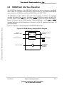
ROM/Flash Interface Operation
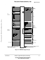
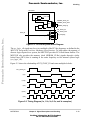
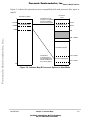
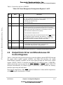
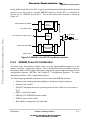
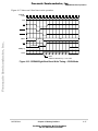
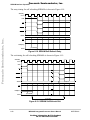
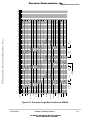
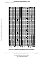
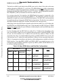
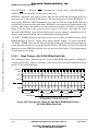
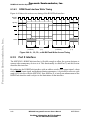
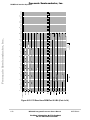
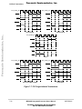
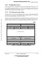
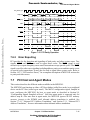
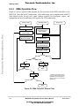
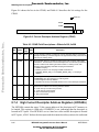
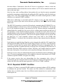
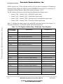
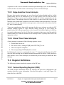
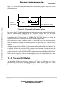
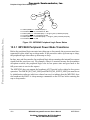
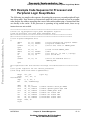
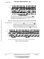
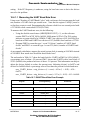
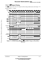
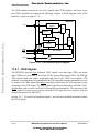
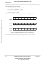
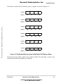
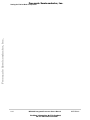
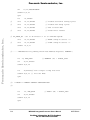
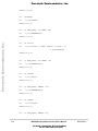
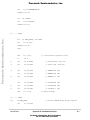
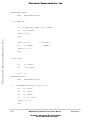
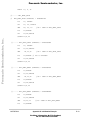
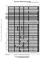
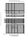
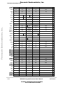
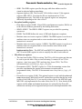
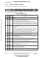
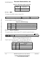
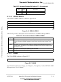
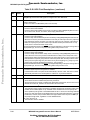
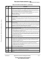
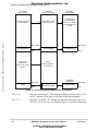
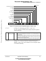
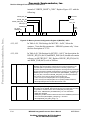
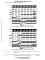
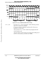
Figure 6-43 shows a cache block read access for the 8-bit data path. Word and double-word
accesses require using the cache-line read access timing shown in Figure 6-43.
Burst read
SDRAM_
CLKn
A[0:19]1
RCSn
Freescale Semiconductor, Inc...
FOE
DATA
(2 +ROMFAL)
x 8 cycles
3 cycles
(constant)2
2 cycles
New fetch begins
between bursts
(minimum)2
Repeated 4 times for complete burst
1 Address toggles for each of 8 single-byte addresses
2 In-line mode adds an additional clock
ROMFAL (ROM first access latency) = 0–31 cycles
Figure 6-43. 8-Bit ROM/Flash Interface—Cache-Line Read Timing
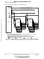
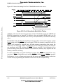
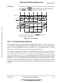
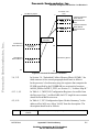
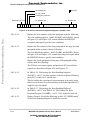
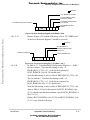
The following paragraphs describe Figure 6-45 in details. Note that ‘a’ represents the actual
data transaction and ‘b’ represents recovery:
1a) RCSn is asserted (low) for the 8 transfers needed to gather the first doubleword
(8 bytes). The ROM address will increment every ROMFAL + 2 cycles.
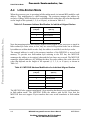
1b) RCSn is negated (high) for 3 cycles for Registered Buffer Mode or 4 cycles for
In-Line Buffer Mode.
2a) RCSn is asserted for the 8 transfers needed to gather the second doubleword.
2b) RCSn is negated for 3 or 4 cycles depending on the buffer mode (as above in 1b).
3a) RCSn is asserted for the 8 transfers needed to gather the third doubleword.
3b) RCSn is negated for 3 or 4 cycles, depending on the buffer mode (as above in
1b).
4a) RCSn is asserted for the 8 transfers needed to gather the fourth double.word.
4b) RCSn is negated for 5 cycles for Registered Buffer Mode (3+2) or 7 cycles for
In-Line Buffer Mode (4+3).
MOTOROLA
Chapter 6. Memory Interface
For More Information On This Product,
Go to: www.freescale.com
6-65