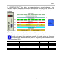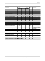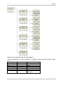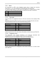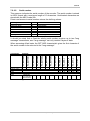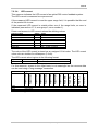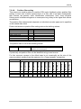
1
HIPERFACE DSL MANUAL HIPERFACE DSL HIPERFACE DSL INTERFACE E Manual HIPERFACE DSL ® ©SICK STEGMANN GmbH All rights reserved. No component of the description may by copied or processed in any other way without the written consent of the company. ® This documentation applies to the HIPERFACE DSL , release version 1.05, release date May 31, 2013. Subject to modification without notice. SICK STEGMANN GmbH accepts no responsibility for the non-infringement of patent rights, e.g. in the case of recommendations for circuit designs or processes. The trade names listed are the property of the relevant companies. HIPERFACE® and HIPERFACE DSL® are registered trademarks of SICK STEGMANN GmbH. SICK STEGMANN GmbH Dürrheimer Strasse 36 78166 Donaueschingen, Germany Tel.: +(49) 771 / 807 – 0 Fax: +(49) 771 / 807 – 100 Internet: http://www.sick.com/ E-mail: [email protected] Made in Germany, 2013. 8013607/ XH05 SICK STEGMANN GmbH Subject to change without notice 1 Manual HIPERFACE DSL ® Table of contents 1. 1.1. 1.2. 1.3. 1.4. Scope of application of the document ......................................................................................... 3 Symbols used .............................................................................................................................. 3 ® HIPERFACE DSL for Motor Feedback ...................................................................................... 4 ® Features of HIPERFACE DSL ................................................................................................... 5 Associated documents ................................................................................................................ 6 2. 2.1. 2.2. 2.3. 2.4. 2.5. Protocol overview ........................................................................................................................ 7 Process data channel ................................................................................................................ 10 Safe Channel ............................................................................................................................. 10 Safe Channel 2.......................................................................................................................... 11 Parameters Channel ................................................................................................................. 11 SensorHub Channel .................................................................................................................. 12 3. 3.1. 3.2. 3.3. Hardware installation ................................................................................................................. 13 Interface circuit .......................................................................................................................... 13 FPGA IP Core ........................................................................................................................... 16 Cable specification .................................................................................................................... 23 4. 4.1. 4.2. 4.3. 4.4. 4.5. 4.6. Interfaces ................................................................................................................................... 25 Interface 1 ................................................................................................................................. 26 Interface 2 ................................................................................................................................. 26 SPI PIPE Interface .................................................................................................................... 27 Control signals ........................................................................................................................... 29 Reset ......................................................................................................................................... 31 Test signals ............................................................................................................................... 31 5. 5.1. 5.2. 5.3. 5.4. 5.5. Register diagram ....................................................................................................................... 34 Explanation of the registers ....................................................................................................... 35 Online Status ............................................................................................................................. 36 DSL Master function register on Channel 1 .............................................................................. 40 DSL Master function register on Channel 2 .............................................................................. 71 Function register for the DSL Slave .......................................................................................... 77 6. 6.1. 6.2. 6.3. 6.4. 6.5. 6.6. 6.7. Central functions ....................................................................................................................... 81 System start .............................................................................................................................. 81 System diagnostics ................................................................................................................... 82 Fast position .............................................................................................................................. 84 Safe position, Channel 1 ........................................................................................................... 87 Safe position, Channel 2 ........................................................................................................... 88 Parameters Channel ................................................................................................................. 90 Status and error messages ....................................................................................................... 99 7. 7.1. 7.2. Motor feedback system resources .......................................................................................... 108 Access to resources ................................................................................................................ 108 Resources list .......................................................................................................................... 111 Keywords index ................................................................................................................................... 165 Glossary............................................................................................................................................... 166 Versions ............................................................................................................................................... 167 2 SICK STEGMANN GmbH Subject to change without notice Manual HIPERFACE DSL ® 1. Scope of application of the document 1.1. Symbols used Note/tip Notes refer to special features of the device. Please pay attention to these notes. They often contain important information. Tips provide additional information that facilitates using the documentation. ACHTUNG CAUTION Safety notes Safety notes contain information about specific or potential dangers, and misuse of the application. This information is to prevent injury. Read and follow the safety notes carefully. 8013607/ XH05 SICK STEGMANN GmbH Subject to change without notice 3 Manual HIPERFACE DSL ® 1.2. HIPERFACE DSL® for Motor Feedback This document describes the use and implementation of the HIPERFACE DSL® data protocol installed in motor feedback systems of servo drives. HIPERFACE DSL® is a purely digital protocol that requires a minimum of connection cables between frequency inverter and motor feedback system. The robustness of the protocol enables the connection to the motor feedback system via the motor connection cable. Motor feedback systems with the HIPERFACE DSL® interface can be used across all performance ranges and substantially simplify the installation of an encoder system in the drive: Standardized digital interface (RS485) Analog components for the encoder interface are not required Standardized interface between the frequency inverter application and the protocol logic Drive OK … MFB system DSL connection Figure 1: Drive system with HIPERFACE DSL Motor ® Based on the name for the predecessor protocol, the SICK HIPERFACE ®, the name HIPERFACE DSL® stands for HIgh PERformance InterFACE Digital Servo Link. This interface takes into account all the current requirements of digital motor feedback systems and also contains future enhancements for the manufacturers of frequency inverters. 4 SICK STEGMANN GmbH Subject to change without notice Manual HIPERFACE DSL ® 1.3. Features of HIPERFACE DSL® Some of the main advantages of HIPERFACE DSL® are based on the opportunity for connection of the encoder: A digital interface on the frequency inverter for all communication with the motor feedback system. The interface complies with the RS485 standard with a transfer rate of 9.375 MBaud. Communication with the encoder via a dual cable Power supply and communication with the encoder can be carried out using the same dual cable. This is possible by the enhancement of the frequency inverter with a transformer. The connection cables to the encoder can be routed as a shielded, twistedpair cable in the power supply cable to the motor. This means that no encoder plug connector to the motor and to the frequency inverter is necessary. The cable length between the frequency inverter and the motor feedback system can be up to 100 m, without degradation of the operating performance. The digital HIPERFACE DSL® protocol can be used for a variety of frequency inverter applications: For the feedback cycle of the frequency inverter's synchronous cyclic data that enables synchronous processing of position and rotation speed of the encoder. Shortest possible cycle time: 12.1 µs. Transmission of the safe position of the motor feedback system with a maximum cycle time of 192 µs. Redundant transmission of the safe position of the motor feedback system with a maximum cycle time of 192 µs, so that suitable motor feedback systems can be used in SIL2 applications (in accordance with IEC 61508). Transmission of the safe position of the motor feedback system on a second channel with a maximum cycle time of 192 µs, so that suitable motor feedback systems can be used in SIL3 applications (in accordance with IEC 61508). Parameter data channel for bi-directional general data transfer with a band width of up to 340 kBaud. This data includes an electronic type label for designation of the motor feedback system and for storage of frequency inverter data in the motor feedback system. SensorHub channel via which motor data from external sensors is transmitted, that are connected by the HIPERFACE DSL® SensorHub protocol to the motor feedback system. 8013607/ XH05 SICK STEGMANN GmbH Subject to change without notice 5 Manual HIPERFACE DSL ® The protocol is integrated into the frequency inverter in the form of hardware logic. This logic circuit is supplied by several manufacturers as an IP Core for FPGA components (FPGA = Field Programmable Gate Array). The available protocol logic enables free routing when installing the HIPERFACE DSL® IP Core. The protocol circuit can be installed along with the frequency inverter application on the same FPGA. Choice between full-duplex SPI interface (SPI = serial peripheral interface) or parallel interface between protocol logic and frequency inverter applications for standardized access to process data (position, rotation speed) and parameters. Fast additional full-duplex SPI interface between protocol logic and frequency inverter applications for standardized access to secondary position data Additional configurable SPI interfaces for output of the data from external sensors. Configurable interrupt output 1.4. Associated documents Along with this manual, the following documents are relevant for the use of the HIPERFACE DSL® interface: Document number Title ® 8 013 664 HIPERFACE DSL safety manual 8 013 737 DSL Master IP Core user manual Table 1: Associated documents Status 8/24/2012 5/31/2013 Individual encoder types with the HIPERFACE DSL® interface are described with the following documents: Data sheet Operating instructions Errata document 6 SICK STEGMANN GmbH Subject to change without notice Manual HIPERFACE DSL ® 2. Protocol overview HIPERFACE DSL® is a fast digital protocol for motor feedback systems for the connection between servo drive and motor feedback system. The protocol is installed in the transport layer in the frequency inverter using a digital logic circuit (DSL Master IP Core). The position data are generated in two different ways in HIPERFACE DSL®, either in free running mode, in which the position values are sampled and transmitted as quickly as possible, or in SYNC mode, in which the position data are sampled and transmitted synchronously with a defined clock signal. With a frequency inverter application, this clock signal is normally the clock feedback of the frequency inverter. In SYNC mode the protocol matches the time points for the sampling of the data without time fluctuations with the clock coming from the frequency inverter. For each frequency inverter cycle at least one position value is sampled and transmitted with constant latency to the DSL Master. As the protocol matches the internal data transfer speed to the frequency inverter cycle, the overall transfer rate of the HIPERFACE DSL® depends on the frequency inverter clock. The protocol package is matched to the various lengths, see Figure 2. Provided the frequency inverter cycle is long enough, additional sampling points can be positioned in the frequency inverter cycle, known as "extra" packages. The number of additional packages is programmed by the user with a distribution value. The number of packages transmitted per frequency inverter cycle cannot be selected at random, as the lower and upper range length of a protocol package must be adhered to. This must be taken into account when setting the distribution value. In free running mode, the frequency inverter cycle is not taken into account for sampling and transmission and the protocol uses the minimum package length. It must be noted that the minimum package length in free running mode is shorter than the minimum package length in SYNC mode. Table 2 shows the dependency of the lengths of the protocol packages using examples for the length of the frequency inverter cycle. 8013607/ XH05 SICK STEGMANN GmbH Subject to change without notice 7 Manual HIPERFACE DSL ® Figure 2: Length of protocol packages Inverter cycle frequency (kHz) Length of the frequency inverter cycle (µs) Length of the protocol package (µs) 2 500 12.50 4 250 12.50 6.25 160 13.33 8 125 12.50 16 62.5 12.50 40 25 12.50 41 to 84 23.8 to 12.1 23.8 to 12.1 Free running -11.52 Table 2: Frequency inverter cycle and length of protocol packages 8 SICK STEGMANN GmbH Subject to change without notice Protocol packages per frequency inverter cycle 40 20 12 10 5 2 1 -- Manual HIPERFACE DSL ® In HIPERFACE DSL®, the data are transmitted over several channels. Each individual channel is adapted to different requirements according to its content. The cycle time of each individual channel varies with the length of the basic protocol package. Figure 3: Data channels in HIPERFACE DSL® Table 3 gives an overview of the characteristics of the various channels. It should be noted that the minimum cycle time and the maximum band width only apply if the maximum number of sample points per frequency inverter cycle was programmed (refer to "Register synchronization control", section 5.3.2). Channel in Function ® HIPERFACE DSL Process data channel Fast position, rotation speed Safe Channel Safe position, status of Channel 1 Safe Channel 2 Safe position, status of Channel 2 Parameter channel General data, parameters SensorHub channel External data Table 3: Channels for protocol data 8013607/ XH05 Cycle time (µs) 12.1 to 23.9 96.8 to 191.2 96.8 to 191.2 Variable 12.1 to 23.9 SICK STEGMANN GmbH Subject to change without notice Band width (kBaud) 1321 to 669 660 to 334 660 to 334 330 to 167 660 to 334 9 Manual HIPERFACE DSL ® 2.1. Process data channel The position value of the motor feedback system is transferred on the process data channel synchronously with the position requests that are controlled by the signal at the SYNC input of the frequency inverter cycle. The process data channel is the fastest channel of the HIPERFACE DSL® protocol. Every protocol package transferred contains a complete update of the content of this channel. This content consists of increments to rotation speed and fast position that are used as feedback parameters for the control loop of the motor drive (see sections 5.3.11 and 5.3.12). If the fast position from the process data channel cannot be calculated (either due to transmission or due to sensor errors), estimation is made by the DSL Master based on the last two available position values of the Safe Channel. The worst case deviation from the actual mechanical position is also provided. ACHTUNG CAUTION Because of the coding during the transfer of the process data channel, there is an upper range limit for both rotation speed and acceleration of the encoder shaft. These range limits are set out in Table 8 and must be adhered to. 2.2. Safe Channel The safe position value of the motor feedback system is transferred on the Safe Channel as an absolute value. In addition, the status of the encoder is reported on this channel in the form of errors and warnings. The safe position value transferred on the Safe Channel is not synchronous with the frequency inverter cycle signal at the SYNC input. The safe position is used by the DSL Master IP Core to check the fast position value of the process data channel and can be used by the frequency inverter application for the same purpose. Where there are deviations between the safe and the fast position values, an error message is generated (see section 6.6). In this case, the protocol replaces the fast position with the safe position. In each package of the safe channel, a collection of status bits is transferred that reflects the error and warning condition of the motor feedback system. It should be noted that each bit of the status byte of the Safe Channel consists of a collection of eight individual motor feedback system bits. Each separate status of the encoder can be selected with a "short message" (see section 6.6.1). 10 SICK STEGMANN GmbH Subject to change without notice Manual HIPERFACE DSL ® 2.3. Safe Channel 2 In Safe Channel 2, the safe position value and the status of the motor feedback system secondary channel are transferred. The channel is for diagnostics in a safety oriented application. The position value transferred on Safe Channel 2 is not synchronous with the frequency inverter cycle signal at the SYNC input. The Safe Channel 2 is only available in the "safety" variants of the DSL Master IP Core. The position value of Safe Channel 2 is either routed via a second processing channel in the DSL encoder (SIL2 system) or from a separate sensor source (SIL3 system). In order to identify transmission errors or errors in the processing of the sensor signal, the user application must use the position value of Safe Channel 2 as a crosscheck against the position value of the primary Safe Channel. The safety requirements are described in the HIPERFACE DSL® Safety Implementation Manual. A status byte is transferred in each package of Safe Channel 2 that reflects the error and warning status of Channel 2 of the motor feedback system. 2.4. Parameters Channel The Parameters Channel is the interface, over which the frequency inverter application reads and writes parameters of the motor feedback system. In addition to the main task of position measurement, motor feedback systems with the HIPERFACE DSL® interface also have various internal resources installed. These resources are accessible via the Parameters Channel. Examples of these resources are temperature measurements, monitoring mechanisms for correct functioning, product data (the "electronic type label") or freely programmable data fields. It should be noted that the resources actually installed for DSL products differ and are listed in the relevant product data sheet. There are two types of communication on the Parameters Channel: - "Short message" transaction - "Long message" transaction A "short message” transaction allows access to resources that have an influence on the HIPERFACE DSL® protocol interface and are used for monitoring them. This includes detailed status and error messages for the motor feedback system and indications of the signal strength on the DSL connection. As a "short message" transaction is processed directly by the interface logic of the motor feedback system, this transaction is completed in a comparatively short time. 8013607/ XH05 SICK STEGMANN GmbH Subject to change without notice 11 Manual HIPERFACE DSL ® A "long message" transaction allows access to all the other resources of the motor feedback system. Unlike a "short message" transaction, a "long message" normally requires processing by the motor feedback system processor and therefore has does not have a response time that can be defined in advance. It should be noted that in HIPERFACE DSL®, a maximum of one "short message" and one "long message" are processed at any time. 2.5. SensorHub Channel Data from additional external sensors can be transferred on the SensorHub Channel that can be used in the frequency inverter system. External sensors must be connected to the motor feedback system via the HIPERFACE DSL® SensorHub interface. Various sensors or sensor networks are accessible via this interface and can be selected using HIPERFACE DSL®. The configuration of external sensors is carried out via the Parameters Channel, whilst the data are selected via the SensorHub Channel. The transfer of protocol packages in the SensorHub Channel takes place synchronously with the DSL transfer and as an extension of the frequency inverter cycle signal that is present at the DSL Master SYNC input. Depending on the use of the SensorHub interface, external data can therefore be sampled and transferred synchronously. The protocol in the SensorHub Channel is not monitored by HIPERFACE DSL®. Apart from the monitoring of the data transfer quality, there are no protocol mechanisms on this channel. A description of the SensorHub interface can be found in the HIPERFACE DSL® SensorHub manual. Figure 4: HIPERFACE DSL® SensorHub interface 12 SICK STEGMANN GmbH Subject to change without notice Manual HIPERFACE DSL ® 3. Hardware installation The installation of HIPERFACE DSL® in a drive system requires an interface circuit with special components as well as the installation of a digital logic core for an FPGA component. The interface circuit is described thoroughly in this chapter. The chapter also contains recommendations for the selection of components. The digital logic core (IP Core) is supplied by SICK for prescribed FPGA types. In addition, the type of cable recommended for the connection between the frequency inverter and the motor feedback system is described thoroughly in this chapter. It may also be possible to use other sorts of cable. These must be tested before use, however. As a physical layer, HIPERFACE DSL® uses a transfer in accordance with EIA-485 (RS-485). Valid RS-485 interface drivers must comply with the conditions in Table 4. Characteristic Value Transfer rate >20 Permitted common mode voltage -7 to +12 Receiver: Differential threshold < 200 voltage Load resistance < 55 Receiver running time delay < 60 Sender running time delay < 60 Sender power-up delay < 80 Sender power-down delay < 80 Sender rise time < 10 Sender dropout time < 10 Protection against short-circuit Protection against bus conflict Table 4: Valid RS-485 interface drivers Units MBaud V mV Ohm ns ns ns ns ns ns 3.1. Interface circuit HIPERFACE DSL® can be used in connection with two different interface circuit configurations. Each configuration requires a different sort of connection cable (see section 3.3). Please note that the use of four core cable is no longer recommended for the motor cable. 3.1.1. Separate encoder cable - four core cable When using a separate encoder cable (see section 3.3.1), the smallest interface circuit can be used. The separate encoder cable requires a four core connection. In connection with the associated table, Figure 5 below gives the specification of the interface circuit. 8013607/ XH05 SICK STEGMANN GmbH Subject to change without notice 13 Manual HIPERFACE DSL ® C1 DSL EN U2 7..12 VDC DE VCC RE\ PWR+ DSL IN R DATA+ DSL OUT D A VSS C2 R1 R2 B DATAPWRFigure 5: Interface circuit with separate encoder cable Recommended components for the interface circuit are set out in Table 5 Component C1 C2 R1, R2 U2 Part Manufacturer 100 nF 2.2 µF, 16 V 56R SN65LBC176A Texas Instruments SN75LBC176A Texas Instruments MAX13431E Maxim IC Table 5: Components for the interface circuit with separate encoder cable. 3.1.2. Ceramic capacitor Ceramic capacitor Resistors RS485 transceiver Integrated cable - two core cable For a connection via a two core cable integrated in the motor cable, (see section 3.3.2), the data cables must be provided with a transformer to raise the common mode rejection ratio. To feed the supply voltage into the data cables choke coils are also required. In connection with the associated table, Figure 6 below gives the specification of the interface circuit. C1 DSL EN DSL IN DSL OUT U2 7..12 VDC DE VCC RE\ TR1 R A C2 C3 L1 DSL+ R1 D VSS B R2 C4 DSLL2 Figure 6: Interface circuit with two core cable (integrated in cable) Recommended components for the interface circuit are set out in Table 6. 14 SICK STEGMANN GmbH Subject to change without notice Manual HIPERFACE DSL Component C1 C2 C3, C4 L1, L2 ® Part Manufacturer 100 nF 2.2 µF, 16 V 470 nF, 50 V B82462A2104K000, 100 µH Epcos ELL6SH101M, 100 µH Panasonic R1, R2 Resistors 56R U2 RS485 transceiver SN65LBC176A Texas Instruments SN75LBC176A Texas Instruments MAX13431E Maxim IC TR1 Transformer PE-68386NL Pulse Engineering 78602/1C Murata B78304B1030A003 Epcos 78602/1C Epcos Table 6: Components of the interface circuit with two core cable (integrated in cable) 3.1.3. Ceramic capacitor Ceramic capacitor Ceramic capacitor Choke coils Motor feedback voltage supply Motor feedback systems with HIPERFACE DSL® have been developed for operation with a supply voltage of 7 to 12 V. The voltage supply is measured at the encoder plug connector. Table 7 below describes the specification for the power supply. Parameter Value Switch-on voltage ramp Max. 180 ms from 0 to 7 V Max. 3.5 A (0 to100 µs) Max. 1 A (100 µs to 400 µs) Max. 250 mA at 7 V Inrush current Operating current Table 7: Voltage supply 8013607/ XH05 SICK STEGMANN GmbH Subject to change without notice 15 Manual HIPERFACE DSL ® 3.2. FPGA IP Core The frequency inverter system communicates with the DSL motor feedback system via a special protocol logic circuit that is designated as the DSL Master. The circuit is installed in an FPGA component and supplied by SICK. The circuit is supplied as an Intellectual Property Core (IP Core) along with a test circuit (test setup). The DSL Master IP Core is supplied in the form of a net list that can be freely connected within the FPGA. If there is sufficient space in the FPGA being used, the DSL Master can be installed in the same component as the frequency inverter application. The IP Core is available as "safety" variant with a dual-channel interface to the frequency inverter or as a "standard" variant, which is smaller and has only one interface. In order that various types of components - e.g. FPGA internal bus or an external processor - can be connected in the best way possible, various open source interface blocks are supplied with the IP Core. Details of the available interface blocks are set out in the IP Core manual (see Chapter 1.4). The following figures show the possible combinations of IP Core and interface block variants. 16 SICK STEGMANN GmbH Subject to change without notice Manual HIPERFACE DSL clk “Safety“ DSL Master (dslm_s) 75 MHz clock Reset, high active clk rst DSL out DSL enable DSL in dsl_out dsl_en dsl_in Servo cycle sync Link indication link SensorHub SPI clock SensorHub SPI select SensorHub SPI data dsl_a dsl_di 16 dsl_do Internal A/D bus channel 1 Internal signals channel 1 dsl_freeze dsl_8n16 bigend spipipe_clk spipipe_ss spipipe_miso Parallel interface Event indications rst sample pos_estimated vrt_error vpos_error acc_not_valid acc_thr_err err8b10b 7 16 dsl_ce_l dsl_oe_l dsl_we_l dsl_wait online_status Debug: “bit sampling“ Debug: “position estimated“ Debug: “safe pos comm. error“ Debug: “safe pos error“ Debug: “accel. invalid“ Debug: “accel. thresh. error“ Debug: “8b/10b error“ ® online_status2 Internal A/D bus channel 2 Internal signals channel 2 clk spi_clk spi_sel spi_miso spi_mosi SPI interface bigend interrupt pos_ready syncd maxdev Select byte sequence Event interrupt Position available Copy of servo cycle Max. position deviation Figure 7: Block circuit diagram of the "safety" DSL Master IP Core with 1 parallel and 1 SPI interface. 8013607/ XH05 SICK STEGMANN GmbH Subject to change without notice 17 Manual HIPERFACE DSL ® rst “Safety“ DSL Master (dslm_s) 75 MHz clock Reset, high active clk rst DSL out DSL enable DSL in dsl_out dsl_en dsl_in Servo cycle sync Link indication link online_status Internal A/D bus channel 1 Internal signals channel 1 spi_clk spi_sel spi_miso spi_mosi SPI interface rst SensorHub SPI clock SensorHub SPI select SensorHub SPI data spipipe_clk spipipe_ss spipipe_miso clk online_status2 Internal A/D bus channel 2 Internal signals channel 2 clk spi_clk spi_sel spi_miso spi_mosi SPI interface Debug: “bit sampling“ Debug: “position estimated“ Debug: “safe pos comm. error“ Debug: “safe pos error“ Debug: “accel. invalid“ Debug: “accel. thresh. error“ Debug: “8b/10b error“ sample pos_estimated vrt_error vpos_error acc_not_valid acc_thr_err err8b10b bigend interrupt pos_ready syncd maxdev Select byte sequence Event interrupt Position available Copy of servo cycle Max. position deviation Figure 8: Block circuit diagram of the "safety" DSL Master IP Core with 2 SPI interfaces. 18 SICK STEGMANN GmbH Subject to change without notice Manual HIPERFACE DSL clk “Standard“ DSL Master (dslm_n) 75 MHz clock Reset, high active clk rst DSL out DSL enable DSL in dsl_out dsl_en dsl_in Servo cycle sync Link indication link SensorHub SPI clock SensorHub SPI select SensorHub SPI data 7 16 dsl_ce_l dsl_oe_l dsl_we_l dsl_wait dsl_freeze dsl_8n16 bigend spipipe_clk spipipe_ss spipipe_miso sample pos_estimated vrt_error vpos_error acc_not_valid acc_thr_err err8b10b dsl_a dsl_di 16 dsl_do Internal A/D bus channel 1 Internal signals channel 1 Parallel interface online_status Debug: “bit sampling“ Debug: “position estimated“ Debug: “safe pos comm. error“ Debug: “safe pos error“ Debug: “accel. invalid“ Debug: “accel. thresh. error“ Debug: “8b/10b error“ ® bigend interrupt pos_ready syncd maxdev Event indication Select byte sequence Event interrupt Position available Copy of servo cycle Max. position deviation Figure 9: Block circuit diagram of the "standard" DSL Master IP Core with one parallel interface. 8013607/ XH05 SICK STEGMANN GmbH Subject to change without notice 19 Manual HIPERFACE DSL ® rst “Standard“ DSL Master (dslm_n) 75 MHz clock Reset, high active clk rst DSL out DSL enable DSL in dsl_out dsl_en dsl_in Servo cycle sync Link indication link SensorHub SPI clock SensorHub SPI select SensorHub SPI data online_status Internal A/D bus channel 1 Internal signals channel 1 clk spi_clk spi_sel spi_miso spi_mosi SPI interface spipipe_clk spipipe_ss spipipe_miso Debug: “bit sampling“ Debug: “position estimated“ Debug: “safe pos comm. error“ Debug: “safe pos error“ Debug: “accel. invalid“ Debug: “accel. thresh. error“ Debug: “8b/10b error“ sample pos_estimated vrt_error vpos_error acc_not_valid acc_thr_err err8b10b bigend interrupt pos_ready syncd maxdev Select byte sequence Event interrupt Position available Copy of servo cycle Max. position deviation Figure 10: Block circuit diagram of the "standard" DSL Master IP Core with one SPI interface. 20 SICK STEGMANN GmbH Subject to change without notice Manual HIPERFACE DSL ® Value Parameter Minimum 74.9925 Typical System Clock 75.0000 Interface characteristics Cable transfer rate 9.375 Reset duration 0.02 0.06 Recovery time after communication errors Characteristics of the motor feedback system Position resolution per rotation 24 Number of resolved rotations 16 Rotation speed Acceleration Sampling latency 727 40 40 262,000 670,000 10.1 Characteristics of the host interface Frequency inverter cycle time 12.1 Frame cycle time 12.1 Frame cycle time Duration of the SYNC signal 11.52 0.04 Characteristics of the SPI-PIPE interface blocks SPI-PIPE clock Characteristics of the Parameters Channel Theoretical transfer rate 166 Duration of access to the 167 communications resource Duration of access to the encoder 263 resource Characteristics of the SensorHub Channel Transfer rate 334 Table 8: Characteristics of the DSL Master IP Core Units Remarks MHz 100 ppm MBd µs Reset is High active µs Bit Bit rad/s rad/s² µs 1,950 27 Jitter of the SYNC signal frequency 8013607/ XH05 Maximum 75.0075 µs µs µs µs 2 % 10 MHz 334 kBd The total can be a maximum of 40 bits 24 bit/rotation 24 bit/rotation SYNC trigger up to valid position in SYNC mode in SYNC mode In free running mode The SYNC signal must be inactive for at least 0.04 µs per cycle. In relation to package cycle time 1,100 µs "Short message" 764 µs "Long message" 669 kBd SICK STEGMANN GmbH Subject to change without notice 21 Manual HIPERFACE DSL 3.2.1. ® DSL Master pin assignment Table 9 below contains a description of the pin functions at the DSL Master IP Core. Pin designation rst clk sync interrupt link pos_ready syncd bigend dsl_in dsl_out dsl_en spipipe_sel spipipe_clk spipipe_miso Type Input Input Input Output Output Output Output Input Input Output Output Input Input Output Function Master reset (High active) Clock input Position sampling resolution Configurable interrupt Connection indication Position data availability indication Position sampling resolution indication Byte sequence choice DSL cable, input data DSL cable, output data DSL cable transceiver, activation SensorHub SPI choice Serial clock for SPI SensorHub SPI SensorHub, master output data/slave input data Table 9: Pin functions of the IP Core interface Additional pin functions of the interface blocks are described in chapter 4. 3.2.2. Implementation of the IP Core The implementation of the IP Core is described in the associated manual and is dependent on the choice of interface blocks and target technology (FPGA). Chapter 1.4 lists the supporting documentation. 22 SICK STEGMANN GmbH Subject to change without notice Manual HIPERFACE DSL ® 3.3. Cable specification The cable recommended for connecting the frequency inverter to the HIPERFACE DSL® motor feedback system is specified by the parameters set out in Table 10. These technical data apply to all configurations. In the case of integrated cables (see section 3.3.2), the motor cables are not listed. Characteristic Minimum Typical Length Impedance at 10 MHz 100 110 DC loop resistance Velocity ratio 0.66 Propagation delay 5 Limit frequency 25 Maximum current per cable 0.25 Operating temperature -40 ® Table 10: Technical data for the HIPERFACE DSL cable 3.3.1. Maximum 100 120 0.1 125 Units m /m c ns/m MHz A °C Separate encoder cable - four core cables The recommended cross section of the separate encoder cable with four encoder cables is given in Figure 11. Cable Sheath Outer shield Taping Extender Insulation Wire Shield cord Pair shield Twisted pair, shielded Figure 11: Cross section of the separate encoder cable with four encoder cables 8013607/ XH05 SICK STEGMANN GmbH Subject to change without notice 23 Manual HIPERFACE DSL 3.3.2. ® Integrated cable - two core cable The recommended cross section of the integrated cable with two encoder cables is given in Figure 12. Cable Sheath Outer shield Taping Extender Insulation Wire Shield cord Pair shield Twisted pair, shielded Figure 12: Cross section of the integrated cable with two encoder cables More Informations relating cable construction and installation are available on the Whitepaper “Cable and Connector for HIPERFACE DSL® Motor and Drive Applications. http://www.sick.com/group/EN/home/products/technologies/hiperfacedsl/Pages/hiperfacedsl_documentation.aspx As a reference, the following manufacturers are listed. Supplier Article number Helukabel WT940060U Leoni 95040129A TecniKabel 35492 Table 11: Reference cables 24 SICK STEGMANN GmbH Subject to change without notice Manual HIPERFACE DSL ® 4. Interfaces The IP Core of the DSL Master includes interfaces to the motor feedback system (DSL Slave) and to the frequency inverter application (see Figure 13). The motor feedback system communicates via a DSL connection with the DSL Master. All data channels between the DSL Master and DSL Slave are routed via this connection. Depending on the use in safety-related applications, the frequency inverter is connected via one or two interfaces (choice of SPI or parallel bus ) and several control signals. In addition, the frequency inverter provides a clock signal (CLK) and a reset signal (RST) to the DSL Master IP Core. By means of these signals, a defined start-up performance is achieved. According to the requirements of the particular application, an optional serial interface (SPI-PIPE) can be employed to use the SensorHub Channel (see Section 2.5, SensorHub Channel). The various interfaces correspond to the tasks described in Table 12. Figure 13: DSL system interfaces Interface Interface 1 Interface 2 Type Full duplex SPI -orParallel bus Full duplex SPI SPI PIPE Control signals Test signals SPI with read access Digital in/outputs Digital outputs CLK Digital input RST Digital input DSL Half duplex RS485 Table 12: Interface functions 8013607/ XH05 Function Register-based access to all DSL Master and DSL Slave functions (except secondary position channel and optional SensorHub Channel) Register-based access to the DSL Master secondary position channel Optional register-based access to SensorHub Channel data DSL Master indication and control signals Test signals for development or fault-finding for a DSL controller Clock signal for the IP Core circuit Reset signal for the IP Core circuit Connection to the motor feedback system SICK STEGMANN GmbH Subject to change without notice 25 Manual HIPERFACE DSL ® 4.1. Interface 1 Interface 1 forms the central communications interface between the frequency inverter application and the DSL Master IP Core. The Safe Channel position data can be read via this interface. The functions of the motor feedback system are also accessible via this interface. Interface 1 is the only interface for Register Block 1 (see section 5.3). If the "safety" variant of the DSL Master is used, Interface 1 is one of two channels for installing safety-related functions. In this case, the Safety Installation Manual must be followed. The following signals are available via Interface 1: Pin name Model name online_status(0:15) Output scan_a(0:6) Input scan_di(0:7) Input scan_do(0:7) Output scan_r Input scan_w Input scan_f Input Table 13. Interface 1 signals. Function IP Core status (see section5.2.1) Register address bus Register input data bus Register output data bus Read signal Write signal Freeze signal Example installations of interface blocks for Interface 1 of the DSL Master are supplied together with the IP Core. These examples include a serial SPI interface and a parallel Texas Instruments EMIFA interface. For safety installations, the use of one of the interface blocks supplied is highly recommended. Please refer to the safety manual for details. 4.2. Interface 2 Interface 2 forms the communications interface for the second channel between the frequency inverter application and the DSL Master IP Core. The secondary channel position data for safety-related functions can be read via this interface. Interface 2 is the only interface for Register Block 2 (see section 5.4). Interface 2 is only installed in "safety" variants of the DSL Master. In "standard" variants, Register Block 2 is not accessible. The following signals are available via Interface 2: Pin name Model name online_status2(0:15) Output scan2_a(0:6) Input scan2_do(0:7) Output scan2_f Input Table 14. Interface 2 signals. Function IP Core status (see section 5.2.2) Register address bus Register output data bus Stop signal DSL Master Interface 2 must be connected in accordance with the safety requirements of the Safety Installation Manual via a serial SPI interface. 26 SICK STEGMANN GmbH Subject to change without notice Manual HIPERFACE DSL ® 4.3. SPI PIPE Interface The SPI PIPE is a write-protected Serial Peripheral Interface (SPI). SPI PIPE is an optional communication channel between the frequency inverter application and the DSL Master IP Core. Read processes on the SensorHub Channel can be carried out via this interface. Alternatively, this data can also be read from the registers by standard transactions via Interface 1. The type of access to the SensorHub Channel is selected by setting or deleting the SPPE bits in the SYS_CTRL register (see section 5.3.1). If the SPPE bit is deleted, the data and the status of the SensorHub channel are accessible via the DSL Master PIPE_S (2Dh) and PIPE_D (2Eh) registers. If the SPPE bit is set, the SensorHub Channel is read using the SPI PIPE "Read Pipeline" transaction. SPI PIPE should be activated if, at a fast frequency inverter cycle, the bandwidth of Interface 1 is insufficient to access position and pipeline data, or if the pipeline data is being processed by another frequency inverter application resource. It should be noted that in every case, the configuration of external sensor components at the SensorHub is carried out via the DSL Master Parameters Channel. The SPI PIPE provides only one read access to the SensorHub Channel (see section 2.5, SensorHub Channel). The SensorHub Channel data is kept in a FIFO (First In First Out) buffer that can hold 8 bytes. In addition, for each data byte, status information is also stored in the FIFO buffer (see sections 5.3.21 and 5.3.22). It should be noted that the FIFO buffer can only store 8 bytes of SensorHub Channel data. If the buffer is not read quickly enough, old data will be overwritten. This is indicated by a flag in the FIFO buffer statusinformation. The SPI Master for the SPI PIPE is the frequency inverter application. The SPI functions "Slave Selection" (Pin: spipipe_sel) and "clock" (Pin: spipipe_clk) are controlled by the frequency inverter application. The SPI function "Data, Master input Slave output" (Pin: spipipe_miso) is controlled by the DSL Master. SPI PIPE has the following SPI characteristics: - PHA = 1 (Sampling for clock trailing edge, data changes for clock leading edge) - POL = 0 (Basic clock value) The data with the highest value bit (MSB) is given first. When accessing the SensorHub Channel via the SPI PIPE, the first four bits of the status buffer (0101) show a different value for each transaction, in order to check the correct function of the interface. 8013607/ XH05 SICK STEGMANN GmbH Subject to change without notice 27 Manual HIPERFACE DSL 4.3.1. ® SPI-PIPE timing The time sequence for SPI PIPE is shown in the time sequence diagram (Figure 14) below and in Table 15. a spipipe_clk b c POL=0 d spipipe_sel e spipipe_miso f 1 PHA=1 2 3 4 5 6 7 8 n-1 n Figure 14: SPI-PIPE interface time control Diagram Description reference a Creation of spipipe_sel before spipipe_clk b Time for spipipe_clk high c Time for spipipe_clk low d spipipe_sel pulse width e Delay spipipe_miso after spipipe_sel high f Delay spipipe_miso after spipipe_clk high Table 15: SPI-PIPE time control 4.3.2. Minimum 30 30 30 30 25 25 Maximum Units 70 70 ns ns ns ns ns ns Read pipeline The SPI PIPE transaction "Read Pipeline" is used for access to the FIFO buffer values that contain the data and status of the SensorHub Channel. Symbol Meaning PIPE STATUS SensorHub Channel status (see section 5.3.20) PIPE DATA SensorHub Channel data (see section 5.3.21) Table 16: "Read Pipeline" transaction spipipe_sel spipipe_clk spipipe_miso PIPE STATUS PIPE DATA Figure 15: "Read Pipeline" transaction 28 SICK STEGMANN GmbH Subject to change without notice Manual HIPERFACE DSL ® 4.4. Control signals Various control signals are available between the DSL Master and the frequency inverter application to configure the performance of the IP Core or to carry out fast monitoring of the IP Core status. 4.4.1. SYNC signal sync is a DSL Master digital input. One edge on this pin triggers a position sampling. The polarity of the edge can be programmed using the SPOL bit in the SYS_CTRL (00h) register. The protocol requires a constant frequency of the signal at this pin, with deviations permitted within a set tolerance band. At start-up, the protocol synchronizes the protocol frame with the signal frequency at sync. If the sync signal frequency is outside the tolerance range, re-synchronization of the protocol is triggered. During the time that the re-synchronization is taking place, sampling is carried out until the re-synchronization is complete with a signal generated by the DSL Master IP Core (also see section 6.3.2). In this case it is guaranteed that the fast position data is not older than 30 µs and safe position data is not older than 240 µs. 4.4.2. INTERRUPT signal interrupt is a DSL Master digital output. interrupt is set to "1" if an interrupt condition has been fulfilled in the DSL-Master. The interrupt conditions are set using the registers MASK_H, MASK_L and MASK_SUM (see sections 5.3.5 and 5.3.6). During each write process in one of the registers EVENT_H or EVENT_L, the interrupt output is triggered until the current SPI transaction has ended. 4.4.3. LINK signal interrupt is a DSL Master digital output. link reflects the content of the LINK bit in the MASTER_QM register (see section 5.3.3) and therefore indicates whether the DSL Master has produced a communications link to a connected HIPERFACE DSL® motor feedback system. link is intended to be a control signal for an LED display, but can also be used to control the start-up performance (see section6.1) or for global error handling. link is reset if communication faults are detected. 8013607/ XH05 SICK STEGMANN GmbH Subject to change without notice 29 Manual HIPERFACE DSL 4.4.4. ® POS_READY signal pos_ready is a DSL Master digital output. pos_ready gives the time point for availability of the position values and permits an event-based reading of the position for incorporating latency reduction. A rising edge at pos_ready indicates that the fast and safe positions are available from Channel 1. A falling edge indicates that the safe position is available from Channel 2. pos_ready is always available, even if the position value is invalid or no connection to the encoder has been established. The time control is Figure 16 illustrated below. Figure 16: pos_ready indications. Dependent upon the configuration in the register system control (see section 5.3.1), pos_ready displays either only the availability of positions based on user requirements (edge at sync input) or all transmitted positions. 4.4.5. SYNCD signal syncd is a DSL Master digital output. syncd indicates whether the sync signal was correctly passed to the encoder, or whether the IP Core is still in a synchronization phase. syncd has the value "1" if the offset between the sync signal and sampling edge is shorter than two clock cycles, otherwise "0". 4.4.6. BIGEND signal bigend is a DSL Master digital input. The byte sequence of the address allocation for registers can be influenced via bigend (see section 5.3, 5.4). The byte sequence is based on 32 bit-wide data words. The selection influences the allocation independently of the interface block used. Table 17 below lists the selection options for bigend. Value Address allocation byte sequence 0 Little endian 1 Big endian Table 17: bigend selection. 30 SICK STEGMANN GmbH Subject to change without notice Manual HIPERFACE DSL ® 4.4.7. MAXDEV signal maxdev is a DSL Master digital output. If the fast position from the process data channel cannot be calculated (either due to transmission or due to sensor errors), estimation is made by the DSL Master based on the last two available position values of the Safe Channel. The worst case deviation from the actual mechanical position is also provided, referring to a userdefined parameter for the maximum possible acceleration in the application (fast position acceleration boundary, see ch. 5.3.24). A threshold can be set up for a worst case deviation to raise the maxdev output. The threshold is a user-defined parameter for the maximum tolerable deviation in the application (fast position estimator deviation, see ch. 0). maxdev indicates whether the maximum tolerable deviation is violated (‘1’) or kept (‘0’). 4.5. Reset rst is the reset input of the DSL Master IP Core. After start-up (switching on) of the frequency inverter, a reset procedure is mandatory to return the DSL Master IP Core to its initialization condition. The reset procedure is established by the parameters listed in Table 18 and quoted in Figure 17. Figure 17: Reset procedure Diagram reference Parameters in Table 8 a Reset delay b Duration of the reset signal Table 18: Reset time sequence. Value (cf. Table Variable >60 ns 8) 4.6. Test signals To support development or fault-finding for controllers that have a DSL interface integrated, the DSL Master supplies some test signals. 8013607/ XH05 SICK STEGMANN GmbH Subject to change without notice 31 Manual HIPERFACE DSL 4.6.1. ® SAMPLE signal sample is a DSL Master digital output. The sample signal is set at the sampling time point of each bit that is transmitted from the DSL motor feedback system. It consists of 50 pulses from Channel 1 followed by a bit pause and 10 pulses from Channel 2 of the motor feedback system. Figure 18: Sample signal The sample signal can be used for eye diagrams to measure time and voltage margins during signal transmission. When making the evaluation, signal delays in the DSL Master must be taken into account. The rising edge of the sample signal is offset by 40 ns from the line driver signal. The time delay of the line driver must also be taken into account. Typically this is 13 ns. 4.6.2. POS_ESTIMATED signal pos_estimated is a DSL Master digital output. The pos_estimated signal is set if some event leads to the fast position (see 5.3.11) being invalid and the position estimator supplying the values. Such events are: The DSL motor feedback system reporting a position error A coding error in transmission of the fast position A check-sum error in transmission of the fast position Realignment from fast to safe position The protocol is re-synchronizing following a break in the link The pos_estimated signal can be used to carry out a statistical analysis of the incidence of errors in the DSL system. 4.6.3. VRT_ERROR signal vrt_error is a DSL Master digital output. The vrt_error signal is set if some event leads to the safe position (see 5.3.14) being invalid. Such events are: A coding error in transmission of the safe position A check-sum error in transmission of the safe position 32 SICK STEGMANN GmbH Subject to change without notice Manual HIPERFACE DSL ® The vrt_error signal can be used to carry out a statistical analysis of the incidence of errors in the DSL system. 4.6.4. VPOS_ERROR signal vpos_error is a DSL Master digital output. The vpos_error signal is set if the safe position is not updated or it has never been written since the startup due to a fault of the internal address/data bus. 4.6.5. ACC_NOT_VALID signal acc_not_valid is a DSL Master digital output. The acc_not_valid signal is set if an encoding error was detected after transmission of a fast position value. If the acc_not_valid signal is set the error counter acc_err_cnt will be incremented with each transmission (see Fehler! Verweisquelle konnte nicht gefunden werden.). As soon as the acc_not_valid signal is reset the error counter acc_err_cnt will be set to “0”. 4.6.6. ACC_THR_ERR signal acc_thr_err is a DSL Master digital output. The acc_thr_err signal is set if the threshold programmed in register acc_err_cnt is exceeded. The acc_thr_err signal can be used to implement a fault-tolerant evaluation in the drive. For this the maximum position deviation can be calculated from the number of transmission errors. 4.6.7. ERR8B10B signal err8b10b is a DSL Master digital output. The err8b10b signal is set if the underlying 8B/10B encoding of a DSL frame transmission is disturbed. The err8b10b signal can be used to make a statistical analysis of the bit error rate of a DSL system. 8013607/ XH05 SICK STEGMANN GmbH Subject to change without notice 33 Manual HIPERFACE DSL ® 5. Register diagram The DSL Master is accessible via the register in two different register blocks. Each register block has its own address area (see Table 19). Register block 1 Address area 00h to 7Fh Functions Channel 1, position/status Parameters Channel SensorHub Channel 2 00h to 3Fh Channel 2, position/status Table 19: Register blocks address area. Transactions with the DSL Master registers are carried out by the appropriate read and write operations via either Interface 1 or Interface 2. Optionally, the SensorHub Channel data is accessible via SPI PIPE. In addition, the DSL Slave interface registers are mirrored as decentralized registers in Register Block 1. The address area 40h to 7Fh is intended for this. The addressing of this register is identical to the addressing of the register in the DSL Master. The answer to the transaction is, however, delayed and must be read individually (see under "Short message", in Section 6.6.1). Figure 19 below shows via which interface a connection to which register block is established. Figure 19: Register block interfaces 34 SICK STEGMANN GmbH Subject to change without notice Manual HIPERFACE DSL ® 5.1. Explanation of the registers In the following description of the registers, symbols are used to describe the standard value of a bit following a reset. Additional symbols are used to describe the functions provided to the frequency inverter application for this bit. The bit is described according to the following sample: "Function" "Reset value", e.g. "R/W-0" Function symbol R W C X Meaning Bit can be read. Bit can be set and deleted. Bit can only be deleted. Bit is not installed and will always be read as "0". Table 20: Function symbols for bits Reset value 0 1 x - Meaning The bit is deleted after a reset. The bit is set after a reset. After a reset, the bit has no defined value. In the register diagram: The bit is not installed and will always be read as "0". Table 21: Symbols for bit reset values It should be noted that read access to a bit that can only be described ("W") always returns the value "0". 8013607/ XH05 SICK STEGMANN GmbH Subject to change without notice 35 Manual HIPERFACE DSL ® 5.2. Online Status For each of Interfaces 1 and 2, there is a group of event indicators available. These indicators display events, warnings or errors that are not stored. 5.2.1. Online Status 1 In Interface 1, the Online Status is a non-storing copy of registers EVENT_H and EVENT_L. The static information in these registers must be deleted by the user after the read process, by writing the value "0" to the corresponding bit in the register, whilst the Online Status only shows the current status without storing previous indications. Online Status 1 is given in two bytes. If the SPI interface block is used, Online Status 1 is transmitted in each transaction in the first two bytes over the spi_miso cable. When the parallel bus interface is used at Interface 1, Online Status 1 has 16 dedicated output signals available. It should be noted that when the parallel bus interface is used the 16 signals of the Online Status are not frozen during a read access. If required, the user can insert a Latch (e.g. scan_f signal). All error indications in High Byte are potentially critical and safetyrelated. Suitable measures must be installed in the user application. ACHTUNG CAUTION All error indications in Low Byte relate to non safety-related errors or warnings. Online Status 1, High Byte R-0 INT Bit 7 36 R-0 SUM R-0 VRT R-1 FIX1 R-0 POS R-0 VPOS R-0 QMLW R-0 PRST Bit 0 Bit 7 INT: Status of the Interrupt output This bit represents an exception to the Online Status, as this bit does not relate to an event indication. INT provides the value of the physical INT output so that request management (polling) can be established. The importance of this flag depends on the Interrupt sources monitored. 1 = interrupt output on "High" level 0 = interrupt output on "Low" level Bit 6 SUM: Summary byte 1 = The last valid value from SUMMARY was not zero. The importance of this flag depends on the particular error source that leads to a set SUMMARY (see section 5.3.13). 0 = The last valid value from SUMMARY was zero. SICK STEGMANN GmbH Subject to change without notice Manual HIPERFACE DSL ® Bit 5 VRT: CRC error on the Safe Channel 1 = The last Safe Channel CRC received in Channel 1 was wrong. It is probable that the safe position transmitted from Channel 1 (see section 2.2) is invalid. Suitable measures must be installed in the user application. 0 = The last vertical CRC received in Channel 1 was correct. Bit 4 FIX1: This bit always gives a "1". For SPI interfaces, this is used for checking the spi_miso pin for stuck-at- '0' faults. Bit 3 POS: Fast position invalid 1 = A source of an error in the fast position in Channel 1 was identified or an alignment procedure is currently being carried out. It is probable that the last fast position is invalid. This error is not safety-related, provided the value is within the range limits defined for the DSL system safety functions. In each case, appropriate measures for handling fast position errors must be implemented in the user application. 0 = No fast position error identified in Channel 1. Bit 2 VPOS: Safe position invalid 1 = A source of an error in the safe position in Channel 1 was identified. It is probable that the safe position transmitted from Channel 1 (see section 2.2) is invalid. Suitable measures must be implemented in the user application. 0 = The last safe position received in Channel 1 was correct. Bit 1 QMLW: Quality monitoring at Low level (see section 5.3.3) 1 = Current value of quality monitoring less than 14. 0 = Current value of quality monitoring greater than or equal to 14. Bit 0 PRST: Protocol reset 1 = IP-Core has restarted the protocol. 0 = IP-Core running. 8013607/ XH05 SICK STEGMANN GmbH Subject to change without notice 37 Manual HIPERFACE DSL ® Online Status 1, Low Byte R-0 R-0 POSTX Bit 7 38 R-0 MIN R-0 ANS R-0 FIX0 R-0 RET R-0 FREL R-0 FRES Bit 0 Bit 7-6 POSTX1:POSTX0: Position transmission status 00: Position request is transmitted to the DSL encoder. 01: Safe Channel was correctly transmitted. 10: Fast position present (see section 5.3.11). 11: Safe Channel 2 was correctly transmitted. Bit 5 MIN: Acknowledgment of message initialization 1 = The DSL encoder sends a figure by which the initialization of the Parameter Channel is acknowledged. 0 = Parameter Channel not functioning. Bit 4 ANS: Incorrect answer detected. 1 = The last answer to a long message was damaged. 0 = No error detected in the last answer to a long message. Bit 3 FIX0: This bit always gives a "0". For SPI interfaces, this is used for checking the spi_miso pin for stuck-at-'1' faults. Bit 2 RET: Retry attempt at a "long" or "short" message 1 = An attempt has just been made to resend a "long" or "short" message. 0 = No attempt is made to send a "long" or "short" message. Bit 1 FREL: Channel status for “long message”. 1 = The channel for the “long message” is free. 0 = The channel for the “long message” is in use. Bit 0 FREL: Channel status for the "short message". 1 = The channel for the "short message" is free. 0 = The channel for the "short message" is in use. SICK STEGMANN GmbH Subject to change without notice Manual HIPERFACE DSL 5.2.2. ® Online Status 2 At Interface 2, Online Status 2 provides information about Channel 2 of the DSL encoder. The data always indicate the current status, with previous indications not being stored. Online Status 2 is given in two bytes. If the SPI interface block is used, Online Status 2 is transmitted in each transaction in the first two bytes over the spi_miso pin. All fault indications in Online Status 2 are potentially critical and safety-related. Suitable measures must be installed in the user application. ACHTUNG CAUTION Online Status 2, High Byte X-0 Bit 7 R-0 SUM2 R-0 COM2 R-1 FIX1 X-0 - R-0 POS2 R-0 QMLW R-0 PRST Bit 0 Bit 7 Not implemented: Read as "0". Bit 6 SUM2: Summary byte Channel 2 1 = One of the indications TEST2 or ERR2 is set (see section 5.4.2). The error reaction to this flag depends on the meaning of the bit they are based on. 0 = Neither TEST2 nor ERR2 is set. Bit 5 COM2: Transmission error Channel 2 1 = The last data received in Channel 2 contains a transmission error. It is probable that the safe position transmitted from Channel 2 (see section 2.3) is invalid. Suitable measures must be installed in the user application. 0 = The last data received in Channel 2 was correct. Bit 4 FIX1: This bit always gives a "1". For SPI interfaces, this is used for checking the spi_miso cable for stuck-at-'0' faults. Bit 3 Not implemented: Read as "0". 8013607/ XH05 SICK STEGMANN GmbH Subject to change without notice 39 Manual HIPERFACE DSL Bit 2 Bit 1 Bit 0 ® POS2: Safe position Channel 2 invalid 1 = A source of an error in the safe position in Channel 2 was identified. It is probable that the safe position transmitted from Channel 2 (see section 2.3) is invalid. Suitable measures must be installed in the user application. 0 = The last safe position received in Channel 2 was correct. QMLW: Quality monitoring at Low level (see section 5.3.3) 1 = Current value of quality monitoring less than 14. 0 = Current value of quality monitoring greater than or equal to 14. PRST: Protocol reset 1 = Protocol control unit is rebuilding the stack. 0 = Protocol control unit not functioning. Online Status 2, Low Byte R-0 R-0 POSTX Bit 7 X-0 - X-0 - R-0 FIX0 X-0 - X-0 - X-0 Bit 0 Bit 7-6 POSTX1:POSTX0: Position transmission status POSTX indicates whether a requested position was transmitted. 00: Position request is transmitted to the DSL encoder. 01: Safe Channel was correctly transmitted. 10: Fast position present (see section 5.3.11). 11: Safe Channel 2 was correctly transmitted. Bit 5-4 Bit 3 Not implemented: Read as "0". FIX0: This bit always gives a "0". For SPI interfaces, this is used for checking the spi_miso cable for stuck-at-'1' faults. Bit 2-0 Not implemented: Read as "0". 5.3. DSL Master function register on Channel 1 The protocol logic controls the non-safety-related performance of the DSL Master via the registers in the DSL Master IP Core on Channel 1. In addition, these registers are also used for accessing the position values of Channel 1. 40 SICK STEGMANN GmbH Subject to change without notice Manual HIPERFACE DSL ® Table 22 contains a list of these registers on Channel 1. Addr Designation Bit 7 Bit 6 Bit 5 Bit 4 Bit 3 Bit 2 Bit 1 Bit 0 00h SYS_CTRL PRST MRST FRST LOOP PRDY SPPE SPOL OEN 01h SYNC_CTRL ES 03h MASTER_QM LINK Quality monitoring 04h EVENT_H INT SUM VRT POS VPOS QMLW PRST 05h EVENT_L MIN ANS RET FREL FRES 06h MASK_H MSUM MVRT MPOS MVPOS MQMLW MPRST 07h MASK_L MMIN MANS MRET MFREL MFRES 08h MASK_SUM MSUM7:0 09h EDGES Bit sampling pattern 0Ah DELAY RSSI Cable delay 0Bh VERSION Coding IP Core version number 0Dh ENC_ID2 SCI ENC_ID19:16 0Eh ENC_ID1 ENC_ID15:8 0Fh ENC_ID0 ENC_ID7:0 10h POS4 Fast position, byte 4 11h POS3 Fast position, byte 3 12h POS2 Fast position, byte 2 13h POS1 Fast position, byte 1 14h POS0 Fast position, byte 0 15h VEL2 Speed, byte 2 16h VEL1 Speed, byte 1 17h VEL0 Speed, byte 0 18h SUMMARY SUM7:0 19h VPOS4 Safe position, byte 4 1Ah VPOS3 Safe position, byte 3 1Bh VPOS2 Safe position, byte 2 1Ch VPOS1 Safe position, byte 1 1Dh VPOS0 Safe position, byte 0 1Eh VPOSCRC_H CRC of the safe position, byte 1 1Fh VPOSCRC_L CRC of the safe position, byte 0 20h PC_BUFFER0 Parameters Channel, byte 0 21h PC_BUFFER1 Parameters Channel, byte 1 22h PC_BUFFER2 Parameters Channel, byte 2 23h PC_BUFFER3 Parameters Channel, byte 3 24h PC_BUFFER4 Parameters Channel, byte 4 25h PC_BUFFER5 Parameters Channel, byte 5 26h PC_BUFFER6 Parameters Channel, byte 6 27h PC_BUFFER7 Parameters Channel, byte 7 28h PC_ADD_H LID LDIR LOFF LIND LLEN LADD9:8 29h PC_ADD_L LADD7:0 LID 2Ah PC_OFF_H LOFFADD14:8 2Bh PC_OFF_L LOFFADD7:0 2Ch PC_CTRL LSTA 2Dh PIPE_S POVR PEMP PERR PSCI 2Eh PIPE_D SensorHub FIFO, output 2Fh PC_DATA "Short message" data 38h ACCERR_CNT Acc. error threshold/counter 39h MAXACC Acc. Res. Acc. Mantissa 3Ah MAXDEV_H Max. position deviation, byte 1 3Bh MAXDEV_L Max. position deviation, byte 0 3Fh DUMMY No data Table 22: Description of the registers in DSL Master, Channel 1 8013607/ XH05 SICK STEGMANN GmbH Subject to change without notice Value at reset 0000 0000 0000 0001 0--- 0000 001- 0010 --00 -000 -00- 0000 --00 -000 0000 0000 0000 0000 0000 0000 0100 0001 -000 0000 0000 0000 0000 0000 0000 0000 0000 0000 0000 0000 0000 0000 0000 0000 0000 0000 0000 0000 0000 0000 0000 0000 0000 0000 0000 0000 0000 0000 0000 0000 0000 0000 0000 0000 0000 0000 0000 0000 0000 0000 0000 0000 0000 0000 0000 0000 0000 0000 0000 0000 0000 0000 1000 0000 0000 0000 1000 0000 0000 0000 ---- ---0 ---- 0000 0000 0000 0000 0000 ---0 0000 0000 0000 1111 1111 1111 1111 ---- ---- 41 Manual HIPERFACE DSL 5.3.1. ® System control The system control register SYS_CTRL contains the main control bits of the DSL Master. It should be noted that apart from a reset of the Master, all system control bits can only be set and deleted by the user. Register 00h: System control R/W-0 PRST Bit 7 R/W-0 MRST R/W-0 FRST R/W-0 LOOP R/W-0 PRDY R/W-0 SPPE R/W-0 SPOL R/W-0 OEN Bit 0 Bit 7 PRST: Protocol reset 1 = A forced reset of the protocol status will be initiated. If the bit is deleted, a restart of the connection is triggered. 0 = Normal protocol action Bit 6 MRST: Messages reset 1 = The Parameters Channel is reset. Current short and long messages are discarded. 0 = Normal Parameters Channel action Bit 5 FRST: Pipeline FIFO, reset 1 = The FIFO is reset. Data is not stored and cannot be read. 0 = Normal FIFO access Bit 4 LOOP: Test Interface 1 Value for the read back test for Interface 1. This value has no other purpose. Bit 3 PRDY: POS_READY mode (see section 4.4.4). 1 = pos_ready shows time of receipt of all position transmissions. 0 = pos_ready shows only the time of receipt of position transmissions following a control clock (sync input). Bit 2 SPPE: SPI-PIPE activation 1 = SPI-PIPE activated. Access to pipeline status and data via SPI-PIPE. The registers PIPE_S and PIPE_D are read as "0". 0 = SPI-PIPE deactivated. Access to pipeline status and data via the registers PIPE_S and PIPE_D. 42 Bit 1 SPOL: Polarity of the synchronization pulse 1 = The sync trailing edge is used. 0 = The sync leading edge is used. Bit 0 OEN: Activation of the output 1 = The DSL cables are activated for output to the DSL Slave. 0 = The impedance of the DSL cable is high. SICK STEGMANN GmbH Subject to change without notice Manual HIPERFACE DSL 5.3.2. ® Synchronization control The SYNC_CTRL register for control of the synchronization contains the bit with which the synchronization source for position sampling is controlled. Register 01h: Synchronization control W-0 W-0 W-0 W-0 W-0 W-0 W-0 W-1 ES Bit 7 Bit 7-0 5.3.3. Bit 0 ES: External synchronization 00000000 = Position sampling during free running at the shortest cycle time. All other values = Position sampling with the sync signal synchronized. The value from ES determines the number of position samplings carried out in one sync cycle. The user must match the number of samplings per cycle to the shortest frame length (see section 6.3.2). Quality monitoring The MASTER_QM quality monitoring register contains the quality monitoring value for the data connection. As soon as the DSL Master registers events that indicate an improvement or degradation of the quality of the data connection, these events are indicated as values higher or lower than the quality monitoring value (see Table 23). Protocol event Wrong synchronization in Safe Channel (last byte) st th Wrong synchronization in Safe Channel (1 … 7 bytes) RSSI <1 Wrong encoding in parameter or SensorHub channels Wrong encoding in process data channel Unknown special characters in the protocol package Any identified error in Safe Channel 1 Any identified error in Safe Channel 2 Correct synchronization in Safe Channel Correct CRC value in Safe Channel Table 23: Quality monitoring events Value change in quality monitoring -4 -6 -4 -1 -2 -2 -6 -8 +1 +1 Quality monitoring is initiated with the value "8". The maximum quality monitoring value is "15". This is the standard value during operation. Particular attention must be paid to the quality monitoring value during the development of a DSL drive controller. If a value lower than "15" is indicated, the cause may be a problem with the connection circuit, particularly if the value is continuously displayed. If the quality monitoring value falls below "14", QMLW information is indicated in Online Status 1 and in the EVENT_H register. 8013607/ XH05 SICK STEGMANN GmbH Subject to change without notice 43 Manual HIPERFACE DSL ® If the quality monitoring value falls to "0", a forced reset of the protocol is carried out. This is indicated by the PRST error bit in Online Status 1 and in the EVENT_H register. The MASTER_QM register is write protected. Register 03h: Quality monitoring register R-0 LINK Bit 7 Bit 0 X-0 X-0 X-0 R-0 R-0 R-0 R-0 QM Bit 0 LINK: DSL protocol connection status 1 = Protocol connection between DSL Master and Slave was established. 0 = No connection present or connection error due to a communications error. It should be noted that LINK is also represented at the link interface output (see section 4.4.3). 44 Bit 6-4 Not implemented: Read as "0". Bit 3-0 QM3:QM0: Quality monitoring bits 0000 to 1111: Quality monitoring value. Higher values indicate a better connection. If the quality monitoring reaches the value "0000", a forced reset of the protocol is carried out. SICK STEGMANN GmbH Subject to change without notice Manual HIPERFACE DSL 5.3.4. ® Events The EVENT_H/EVENT_L registers contain the messaging bits for all warning and error modes of the DSL system. All messaging bits are set by the DSL Master if a corresponding status is determined. The following bit description lists the effects of warning and error conditions as well as the reactions to errors that must be installed in the frequency inverter application. An event bit that has been set is not reset by the DSL Master. The frequency inverter application must delete bits that have been set. Both edge and level-sensitive flags are present in the EVENT registers. Edgesensitive bits are set when the corresponding status arises. They are only set again if the corresponding status disappears and then arises once more. This is the standard action. The level-sensitive bits set a bit as long as the corresponding status exists. It should be noted that all event register bits are also transferred to Online Status 1 (see section 5.2.1). The event bits are not static there and contain the actual status of each individual event. Register 04h: High Byte events R-0 INT Bit 7 Bit 7 R/C-0 SUM R/C-1 VRT INT: Interrupt status This bit reflects the (see section 4.4.2). X-0 status R/C-0 POS of R/C-0 VPOS the R/C-1 QMLW interrupt R/C-0 PRST Bit 0 signal Bit 6 SUM: Remote event monitoring 1 = The DSL Slave has signaled an event and the summary mask is set accordingly (see registers MASK_SUM and SUMMARY). 0 = All DSL Slave events are deleted. When the SUM bit is set, an error or a warning has been transmitted from the DSL Slave. The frequency inverter application must check the SUMMARY register (see section 5.3.13) to obtain a detailed description. This bit is level sensitive. Bit 5 VRT: Error on the Safe Channel 1 = Data consistency error on the Safe Channel. 0 = Safe Channel data was correctly transmitted. This error usually indicates a transmission error on the DSL connection. If this error occurs frequently, the wiring of the DSL connection should be checked. If this error occurs continuously, there is probably an error in the motor feedback system. This error affects quality monitoring and produces the QMLW warning or a protocol reset. 8013607/ XH05 SICK STEGMANN GmbH Subject to change without notice 45 Manual HIPERFACE DSL ACHTUNG CAUTION ® When this error occurs, the last valid value of the safe position is retained (see section 5.3.14). Only if a fresh value has been transmitted will the safe position be updated and correspond to the actual position of the motor feedback system. The fast position is not affected by this. Bit 4 Not implemented: Read as "0". Bit 3 ACHTUNG CAUTION POS: Fast position error 1 = Fast position data consistency error 0 = The data for the fast position was correctly transmitted. This error usually indicates a transmission error on the DSL connection. If this error occurs frequently, the wiring of the DSL connection should be checked. If this error occurs continuously, there is probably an error in the motor feedback system. When this error occurs, the fast position is updated by an extrapolation. The last valid rotation speed value is used for this extrapolation. Only if a new valid safe position has been transmitted (see section 5.3.14) is the fast position updated to the actual position of the motor feedback system. This can lead to a temporary (<200 µs) difference between the actual and the transmitted position, particularly during accelerated movement of the drive. Bit 2 VPOS: Safe position error, Channel 1 1 = Sensor error in Channel 1. 0 = The safe position is correct. This error usually indicates an encoder sensor error. If this error occurs continuously, there is probably an error in the motor feedback system. When this error occurs, the error value FD FD FD FD FDh is displayed instead of the safe and fast position in Channel 1. ACHTUNG CAUTION 46 SICK STEGMANN GmbH Subject to change without notice Manual HIPERFACE DSL Bit 1 ® QMLW: Quality monitoring low value warning 1 = Quality monitoring value (see register 03h) below "14" 0 = Quality monitoring value greater than or equal to "14" This warning indicates that a transmission error occurred at bit level for one of the CRC values. If this error occurs frequently, the wiring of the DSL connection should be checked (also see section 5.3.3). Bit 0 Register 05h: PRST: Protocol reset warning 1 = The forced protocol reset was triggered. 0 = Normal protocol action This error message indicates that the protocol connection to the DSL Slave has been re-initialized. This error message can be caused by a frequency inverter application request (PRST bit in SYS_CTRL), generated by the DSL Master itself, or activated via the rst input. The DSL Master causes a protocol reset if too many transmission errors indicate a connection problem (see section 5.3.3). A protocol reset causes a re-synchronization with the DSL Slave that can improve the connection quality. Low Byte events X-0 X-0 R/C-0 MIN R/C-0 ANS R/C-0 R/C-0 RET Bit 7 R/C-0 FREL R/C-0 FRES Bit 0 Bit 7-6 Not implemented: Read as "0". Bit 5 MIN: Message init 1 = An acknowledgment was received from the Slave for the initialization of a message. 0 = No acknowledgment for the initialization received. When this warning is displayed, the Parameters Channel is still in the initialization status and no "short message" or "long message" can be triggered. This bit is level sensitive. Bit 4 ANS: Erroneous answer to "long message" 1 = An error occurred during the answer to a long message. The effectiveness of the previous transaction is not known. 0 = The last answers to "long messages" were error free. This error indicates that the transmission of an answer from the DSL Slave to the last "long message" failed. The frequency inverter application must send the "long message" again. Bit 3 Not implemented: Read as "0". 8013607/ XH05 SICK STEGMANN GmbH Subject to change without notice 47 Manual HIPERFACE DSL 48 ® Bit 2 RET: Fresh attempt at a "long" or "short" message 1 = Due to a transmission error, the answer to the "long message" or "short message" was requested again. 0 = The transmission of the answer to the "long message" or "short message" was error free. This warning indicates that the transmission of a request to the DSL Slave, or the answer from the DSL Slave to the last "long message" or "short message" failed and will be attempted again automatically. If this warning occurs, the wiring of the DSL connection should be checked. If this warning is indicated continuously, there is probably an error in the motor feedback system. Bit 1 FREL: Channel free for "long message" 1 = A "long message" can be sent on the Parameters Channel. 0 = No "long message" can be sent. If the bit is set, the frequency inverter application can trigger a "long message". Provided no answer has been received from the DSL Slave, this bit remains deleted. As the processing duration of a "long message" in the motor feedback system is not specified, a user time limit condition should be installed via the frequency inverter application. When a time limit is exceeded, the MRST bit in the SYS_CTRL register is set, which causes the Parameters Channel to be reset. Bit 0 FRES: Channel free for "short message" 1 = A "short message" can be sent on the Parameters Channel. 0 = No "short message" can be sent. If the bit is set, the frequency inverter application can trigger a "short message". Provided no answer has been received from the DSL Slave, this bit remains deleted. As the processing duration of a "long message" in the motor feedback system is not specified, a time limit condition is installed in the DSL Master. If the time limit is exceeded, attempts are made again automatically (see under RET bit). SICK STEGMANN GmbH Subject to change without notice Manual HIPERFACE DSL 5.3.5. ® Event mask In the event mask registers MASK_H/MASK_L, the events are set with which the interrupt signal is set. Several events can be masked to trigger an interrupt. In addition, events from the DSL Slave summary can be combined with these events (see section 5.3.6). This is explained in Figure 20. Figure 20: Interrupt masking It should be noted that the SUM bit is an OR connection of all bits of the status summary (SUMMARY register). 8013607/ XH05 SICK STEGMANN GmbH Subject to change without notice 49 Manual HIPERFACE DSL Register 06h: ® High Byte event mask X-0 W-0 MSUM W-0 MVRT X-0 W-0 MPOS W-0 MVPOS W-0 MQMLW Bit 7 Bit 7 Not implemented: Read as "0". Bit 6 MSUM: Mask for remote event monitoring 1 = DSL Slave events that are masked in the SUMMARY register set the interrupt signal. 0 = DSL Slave events that are masked in the SUMMARY register do not set the interrupt signal. Bit 5 MVRT: Mask for transmission errors on the Safe Channel 1 = A transmission error on the Safe Channel sets the interrupt signal. 0 = A transmission error on the Safe Channel does not set the interrupt signal. Bit 4 Not implemented: Read as "0". Bit 3 MPOS: Mask for fast position error 1 = An error in the fast position sets the interrupt signal. 0 = An error in the fast position does not set the interrupt signal. Bit 3 MVPOS: Mask for safe position error 1 = An error in the safe position sets the interrupt signal. 0 = An error in the safe position does not set the interrupt signal. Bit 1 MQMLW: Mask for low quality monitoring value warning 1 = A low quality monitoring value (see registers 03h and 05h) sets the interrupt signal. 0 = A low quality monitoring value does not set the interrupt signal. Bit 0 MPRST: Mask for protocol reset warning 1 = A protocol reset sets the interrupt signal. 0 = A protocol reset does not set the interrupt signal. Register 07h: Low Byte event mask X-0 X-0 W-0 MMIN W-0 MANS X-0 W-0 MRET Bit 7 Bit 7-6 Bit 5 50 W-0 MPRST Bit 0 W-0 MFREL W-0 MFRES Bit 0 Not implemented: Read as "0". MMIN: Mask for message initialization confirmation 1 = The acknowledgment for the initialization of a DSL Slave message sets the interrupt signal. 0 = The acknowledgment for the initialization of a DSL Slave message does not set the interrupt signal. SICK STEGMANN GmbH Subject to change without notice Manual HIPERFACE DSL ® Bit 4 MANS: Mask for erroneous answer to long message 1 = A transmission error during the answer to a long message sets the interrupt signal. 0 = A transmission error during the answer to a long message does not set the interrupt signal. Bit 3 Not implemented: Read as "0". Bit 2 MRET: Mask for a fresh attempt at a "long" or "short" message 1 = The fresh request for a "long message" or "short message" sets the interrupt signal. 0 = The fresh request for a "long message" or "short message" does not set the interrupt signal. Bit 1 MFREL: Mask for "channel free for "long message"' 1 = If a "long message" can be sent on the Parameters Channel, the interrupt signal is set. 0 = If a "long message" can be sent on the Parameters Channel, the interrupt signal is not set. Bit 0 MFRES: Mask for "channel free for "short message"' 1 = If a "short message" can be sent on the Parameters Channel, the interrupt signal is set. 0 = If a "short message" can be sent on the Parameters Channel, the interrupt signal is not set. 5.3.6. Summary mask In the MASK_SUM summary mask register, the DSL Slave collective events are determined with which the SUM event monitoring in the event register as well as the signal to the interrupt pin are set (interrupt). Several events can be masked to trigger an interrupt. In addition, events from the DSL Master can be combined with these events (see section 5.3.4). It should be noted that the MSUM bit from the MASK_H register is an OR connection of all bits of the summary mask register. 8013607/ XH05 SICK STEGMANN GmbH Subject to change without notice 51 Manual HIPERFACE DSL ® Register 08h: Summary mask W-0 W-0 W-0 W-0 W-0 W-0 W-0 W-0 MSUM7 MSUM6 MSUM5 MSUM4 MSUM3 MSUM2 MSUM1 MSUM0 Bit 7 Bit 7-0 5.3.7. Bit 0 MSUM7:MSUM0: Mask for status summary bits 1 = In the set status, the corresponding status summary bit sets the SUM event monitoring and the signal at the interrupt pin. 0 = In the set status, the corresponding status summary bit does not set the SUM event monitoring and the signal at the interrupt pin. Edges The EDGES edge register contains the time control for the DSL cable bit sampling and can be used to monitor the connection quality. Each individual edge register bit is set if, at system start-up, an edge of the test signal is detected during the time period of the corresponding bit. An edge is defined as a change in cable value between successive detections. The sampling is carried out eight times as fast as the cable bit rate. Clean cable signals mean that only a few bits are set in the edge register, whilst noisy cable signals set a large number of bits. If all bits in the edge register are set, this is an indication of excessive interference in the cable in which no connection can be established. ACHTUNG CAUTION The register is write protected. The content of this register does not change after the start-up phase. A new bit sampling pattern is only generated after a forced reset of the protocol. Register 09h: Edges R-0 R-0 R-0 R-0 R-0 Bit sampling pattern Bit 7 Bit 7-0 52 R-0 R-0 R-0 Bit 0 Bit sampling pattern: Identification of edges in the cable signal 1 = An edge was detected in the time period of the corresponding bit. 0 = No edge was detected in the time period of the corresponding bit. SICK STEGMANN GmbH Subject to change without notice Manual HIPERFACE DSL ® 5.3.8. Delay The DELAY run time register stores information about the run time delay of the system cable and the signal strength. The register can be used to monitor the connection quality. The register is write protected. Register 0Ah: Run time delay R-0 R-0 R-0 R-0 R-0 RSSI R-0 R-0 Cable delay Bit 7 Bit 7-4 R-0 Bit 0 RSSI: Indication of the received signal strength 4 bit value for the cable signal strength, from "0" to "12". Higher values indicate better connection quality. If the value is less than "1" a forced reset of the protocol is carried out. RSSI is continuously updated during operation and used for signal monitoring during run time. Bit 3-0 Cable delay: 4 bit value for cable delay. This value gives the cable signal round trip delay of cable and transceivers in bits. This value enables a rough estimate of cable length to be made. The value for Line Delay does not change after the start-up phase. A fresh value for Line Delay is only measured after a forced reset of the protocol. Table 24 below shows the relationship between the value in Line Delay and the cable length of the DSL connection. Cable delay DSL connection cable delay 0 <100 ns 1 100 to 200 ns 2 200 to 300 ns 3 300 to 400 ns 4 400 to 500 ns 5 500 to 600 ns 6 600 to 700 ns 7 700 to 800 ns 8 800 to 900 ns 9 900 to 1000 ns Table 24: Cable delay ACHTUNG CAUTION Cable length DSL connection < 10 m 10 to 20 m 20 to 30 m 30 to 40 m 40 to 50 m 50 to 60 m 60 to 70 m 70 to 80 m 80 to 90 m 90 to 100 m A value above "9" indicates a delay of greater than 1 µs. Such a value will lead to a violation of the specification for cycle time. In this case, a check should be made of whether the cable complies with the cable specification. 8013607/ XH05 SICK STEGMANN GmbH Subject to change without notice 53 Manual HIPERFACE DSL 5.3.9. ® Version The VERSION version register contains the release version of the DSL Master IP Core. The register is write protected. Register 0Bh: Version R-0 R-1 Coding R-0 R-1 R-0 Major Release Bit 7 54 Bit 7-6 Coding: Type of IP Core 01= DSL Master IP Core Bit 5-4 IP Core Major release number: The current version is 1 (01). Bit 3-0 IP Core Minor release number: The current version is 5 (0101). SICK STEGMANN GmbH Subject to change without notice R-1 R-0 R-0 Minor Release Bit 0 Manual HIPERFACE DSL ® 5.3.10. Encoder ID The ENC_ID encoder ID registers contain the designation code of the motor feedback system connected to the DSL Master. In the current protocol specification, the designation code is 20 bits long. With later enhancements, the free bits in the encoder ID registers are used to indicate special characters. These registers are write protected. Register 0Dh: Encoder ID, byte 2 X-0 R-0 R-0 SCI R-0 R-0 R-0 R-0 ENC_ID19:16 Bit 23 Register 0Eh: Bit 16 Encoder ID, byte 1 R-0 R-0 R-0 R-0 R-0 ENC_ID15:8 R-0 R-0 Bit 15 Register 0Fh: R-0 R-0 Bit 8 Encoder ID, byte 0 R-0 R-0 R-0 R-0 R-0 ENC_ID7:0 R-0 R-0 Bit 7 R-0 Bit 0 Bit 23 Not implemented: Read as "0". Bit 22-20 SCI: Indication of special characters 3 bit special character for later enhancements of the encoder designation code. Not allocated. Bit 19-0 ENC_ID: Encoder designation code Designation of the motor feedback system (length: 20 bits) The individual ENC_ID register bits are allocated as follows: Bit 19 Continue: In High status, Continue indicates that ENC_ID is longer than 20 bits (for future use). Bit 18 to 16 Reserved: Read as "0". Bit 15 to 12 User defined encoder index: 4 bit value (0 to 15) for userdefined encoder index (see section 7.2.4.7). Bit 11 Reserved: Read as "0". Bit 10 Sign: In High status, Sign indicates that the position value is signed, in Low status, Sign indicates that the position value is not signed. Bit 9 to 4 #Pos-#Acc: Length of position information (standard value: 40 bits) minus length of the acceleration value transmitted (, see section 5.3.11, standard value: 11 bits). Bit 3 to 0 #Acc-8: Length of the acceleration value transmitted (, standard value: 11 bits) minus 8. 8013607/ XH05 SICK STEGMANN GmbH Subject to change without notice 55 Manual HIPERFACE DSL ® 5.3.11. Fast position The POS registers for the fast position contain the value of the motor feedback system connected. This position is generated incrementally from the safe position at start-up and is updated with every protocol frame. After every eight protocol frames, the fast position is checked against the safe position (see under registers 18h to 1Ch). The position sampling point is determined by the ES value of the synchronization control register. Only those POS bits are activated that lie within the range that the motor feedback system has actually measured. All other higher value bits are read as "0". The number of measurable bits can be taken from ENC_ID bits 9 to 0 in the ENC_ID0 to 2 registers. If Sign is set in the ENC_ID register, the value of the fast position is given signed in the two's complement. The units of the position value are (steps). These registers are write protected. Register 10h: Fast position, byte 4 R-0 R-0 R-0 R-0 R-0 Fast position, byte 4 R-0 R-0 Bit 39 Register 11h: Bit 32 Fast position, byte 3 R-0 R-0 R-0 R-0 R-0 Fast position, byte 3 R-0 R-0 Bit 31 Register 12h: Bit 24 R-0 R-0 R-0 R-0 Fast position, byte 2 R-0 R-0 Bit 23 R-0 Bit 16 Fast position, byte 1 R-0 R-0 R-0 R-0 R-0 Fast position, byte 1 Bit 15 56 R-0 Fast position, byte 2 R-0 Register 13h: R-0 SICK STEGMANN GmbH Subject to change without notice R-0 R-0 R-0 Bit 8 Manual HIPERFACE DSL Register 14h: Fast position, byte 0 R-0 R-0 R-0 R-0 R-0 Fast position, byte 0 R-0 R-0 Bit 7 Bit 39-0 ® R-0 Bit 0 Fast position, byte 4/3/2/1/0: Position value of the motor feedback system (length: 40 bits), incrementally generated. 5.3.12. Speed The VEL speed registers contain the speed values of the connected motor feedback system. This value is calculated as a position from the acceleration value ( position) transmitted on the process data channel and the currently updated protocol frame (see section 2). The speed sampling point is determined by the ES value of the SYNC_CTRL register. The units of the speed value are (steps/frame cycle time). These registers are write protected. Register 15h: Speed, byte 2 R-0 R-0 R-0 R-0 R-0 Speed, byte 2 R-0 R-0 Bit 23 Register 16h: Bit 16 Speed, byte 1 R-0 R-0 R-0 R-0 R-0 Speed, byte 1 R-0 R-0 Bit 15 Register 17h: Bit 8 R-0 R-0 R-0 R-0 Speed, byte 0 R-0 R-0 Bit 7 8013607/ XH05 R-0 Speed, byte 0 R-0 Bit 23-0 R-0 R-0 Bit 0 Speed, byte 2/1/0: Speed of the motor feedback system (length: 24 bits) SICK STEGMANN GmbH Subject to change without notice 57 Manual HIPERFACE DSL ® 5.3.13. Status summary The SUMMARY status summary register contains the summarized DSL Slave status information. Each status summary bit contains the summarized information from 8 error, warning and event modes of the DSL Slave. The bits in the status summary register can be read and, if set, deleted. Figure 21 shows the relationship between the encoder status registers, the status summary register and the SUM bit in the EVENT registers. Figure 21: DSL Slave status and summary A bit that has been set in the SUMMARY register is not automatically deleted by the DSL System. To delete, the frequency inverter application must read the corresponding DSL Slave encoder status register (see section 5.5.1) and acknowledge the status message, by individually deleting each set bit. Register 18h: Status summary R-0 SUM7 Bit 7 58 R-0 SUM6 R-0 SUM5 R-0 SUM4 R-0 SUM3 R-0 SUM2 R-0 SUM1 R-0 SUM0 Bit 0 Bit 7-1 SUM7:SUM1: Status summary bit (external resource) 1 = An error, a warning or an event associated with DSL Slave external resources was triggered. 0 = The corresponding error, warning or event is not active. Bit 0 SUM0: Status summary bit (interface) 1 = An error, a warning or an event associated with the DSL Slave protocol interface was triggered. 0 = The DSL Slave protocol has not triggered an error, warning or event. SICK STEGMANN GmbH Subject to change without notice Manual HIPERFACE DSL ® 5.3.14. Safe position The VPOS registers for the safe position contain the position value from the primary channel of the motor feedback system connected. This safe position is transmitted in every eighth protocol frame if the validity of the data transfer has been checked. The value for each safe position transmitted is compared with the incrementally generated position value (fast position) (see registers 10h to 14h). The safe position is not synchronized with the sync signal. Only those vpos bits are activated that lie within the range that the motor feedback system has actually measured. All other higher value bits are read as "0". The number of measurable bits can be taken from ENC_ID bits 9 to 0 in the ENC_ID0 to 2 registers. If Sign is set in the ENC_ID register, the value of the safe position is given signed in the two's complement. The units of the position value are [steps]. These registers are write protected. Register 19h: Safe position, byte 4 R-0 R-0 R-0 R-0 R-0 Safe position, byte 4 R-0 R-0 Bit 39 Register 1Ah: Bit 32 Safe position, byte 3 R-0 R-0 R-0 R-0 R-0 Safe position, byte 3 R-0 R-0 Bit 31 Register 1Bh: Bit 24 R-0 R-0 R-0 R-0 Safe position, byte 2 R-0 R-0 Bit 23 Bit 16 R-0 R-0 R-0 R-0 Safe position, byte 1 R-0 R-0 Bit 15 Bit 8 R-0 R-0 R-0 R-0 Safe position, byte 0 Bit 7 8013607/ XH05 R-0 Safe position, byte 0 R-0 Bit 39-0 R-0 Safe position, byte 1 R-0 Register 1Dh: R-0 Safe position, byte 2 R-0 Register 1Ch: R-0 R-0 R-0 R-0 Bit 0 Safe position, byte 4/3/2/1/0: Position value at motor feedback system Channel 1 (length: 40 bits), absolute value transmitted. SICK STEGMANN GmbH Subject to change without notice 59 Manual HIPERFACE DSL ® 5.3.15. Position checksum The POSCRC registers for the position checksum contain the CRC checksum of the safe position VPOS (see section 5.3.14) and the SUMMARY status summary (see section 5.3.13). The CRC is checked in the DSL Master IP Core. In order to guarantee, in a safety related application, that the CRC machine in the IP Core is functioning, these registers can be checked with an external cross check in the diagnostics test interval. This interval is described in the section about safety implementation (see the HIPERFACE DSL® safety implementation manual). The CRC is generated with the following CRC parameters: Parameter CRC sequence CRC polynomial Starting value Closing XOR value Reverse data bytes Reverse CRC before closing XOR Table 25: POSCRC parameters Value 16 Bit 16 15 12 7 6 4 3 C86Ch (x + x + x + x + x + x + x + 1) 0000h 00FFh No No The sequence of the bytes to calculate the CRC is shown in the following figure: SUMMARY VPOS[39:32] VPOS[31:24] VPOS[23:16] VPOS[15:8] VPOS[7:0] Figure 22: Sequence of the bytes to calculate the CRC Register 1Eh: CRC of the safe position, byte 1 R-0 R-0 R-0 R-0 R-0 R-0 CRC of the safe position, byte 1 R-0 Bit 15 Register 1Fh: Bit 8 CRC of the safe position, byte 0 R-0 R-0 R-0 R-0 R-0 R-0 CRC of the safe position, byte 0 Bit 7 Bit 15-0 60 R-0 R-0 R-0 Bit 0 CRC of the safe position: 16 bit CRC checksum (CRC 16) of the safe position and status summary in Channel 1. SICK STEGMANN GmbH Subject to change without notice Manual HIPERFACE DSL ® 5.3.16. Parameters Channel buffer The eight PC_BUFFER registers of the Parameters Channel buffer contain the answer to the last "long message" request or the data for a "long message" write operation. Access to these registers may only take place if the "long message" channel is free (FREL in the EVENT_L register). Depending on the length of the "long message" answer, the registers are used as follows: Length of the "long message" Register used 8 bytes 20h to 27h 4 bytes 20h to 23h 2 bytes 20h to 21h 0 bytes None Table 26: Data length of the "long message" These registers are also for the reporting of error conditions arising from a "long message" operation. If, when accessing a resource, an error due to a "long message" arises (e.g. invalid data, error in the A/D conversion, time overrun), after the answering message has been received the LOFF bit in the PC_ADD_H register (28h) is set. In this case the Parameters Channel buffer bytes 0 and 1 contain an error code. The meaning of the error code depends on the particular HIPERFACE DSL® encoder and is described in detail in the data sheet. Register 20h: Parameters Channel buffer, byte 0 R/W-0 R/W-0 R/W-0 R/W-0 R/W-0 R/W-0 Parameters Channel, byte 0 R/W-0 Bit 63 Register 21h: Bit 56 Parameters Channel buffer, byte 1 R/W-0 R/W-0 R/W-0 R/W-0 R/W-0 R/W-0 Parameters Channel, byte 1 R/W-0 Bit 55 Register 22h: Bit 48 R/W-0 R/W-0 R/W-0 R/W-0 R/W-0 Parameters Channel, byte 2 R/W-0 Bit 47 Bit 40 R/W-0 R/W-0 R/W-0 R/W-0 R/W-0 Parameters Channel, byte 3 R/W-0 Bit 39 Bit 32 R/W-0 R/W-0 R/W-0 R/W-0 R/W-0 Parameters Channel, byte 4 R/W-0 Bit 31 R/W-0 Bit 24 Parameters Channel buffer, byte 5 R/W-0 R/W-0 R/W-0 R/W-0 R/W-0 R/W-0 Parameters Channel, byte 5 Bit 23 8013607/ XH05 R/W-0 Parameters Channel buffer, byte 4 R/W-0 Register 25h: R/W-0 Parameters Channel buffer, byte 3 R/W-0 Register 24h: R/W-0 Parameters Channel buffer, byte 2 R/W-0 Register 23h: R/W-0 SICK STEGMANN GmbH Subject to change without notice R/W-0 R/W-0 Bit 16 61 Manual HIPERFACE DSL Register 26h: ® Parameters Channel buffer, byte 6 R/W-0 R/W-0 R/W-0 R/W-0 R/W-0 R/W-0 Parameters Channel, byte 6 R/W-0 Bit 15 Register 27h: Bit 8 Parameters Channel buffer, byte 7 R/W-0 R/W-0 R/W-0 R/W-0 R/W-0 R/W-0 Parameters Channel, byte 7 Bit 7 62 R/W-0 R/W-0 R/W-0 Bit 0 Bit 63-0 Parameters Channel buffer, byte 0-7: 8 bytes for the answer to a long message (read operation) or for a "long message" write operation. Bit 63-48 Error report for a long message, byte 0-1: 2 bytes for reports about errors in encoder resources arising from the previous "long message" operation. SICK STEGMANN GmbH Subject to change without notice Manual HIPERFACE DSL ® 5.3.17. Long message address The addresses and the addressing mode for "long messages" sent over the Parameters Channel are determined in the PC_ADD_H/PC_ADD_L long message address registers. In addition, the long message address register 28h (PC_ADD_H) contains indications of errors arising from "long message" operations. For this sort of error, the Parameters Channel buffer contains the error code in bytes 0 and 1 associated with this status (see section 6.7.5). Register 28h: Long message address, byte 1 R-1 LID Bit 15 Register 29h: W-0 LRW R/W-0 LOFF W-0 LIND W-0 W-0 LLEN W-0 LADD9 W-0 LADD8 Bit 8 W-0 W-0 Long message address, byte 0 W-0 W-0 W-0 W-0 W-0 LADD7:0 W-0 Bit 7 Bit 0 Bit 15 LID: Long message identification. The value must be "1". Bit 14 LRW: Long message, read/write mode 1 = "long message" read operation 0 = "Long message" write operation Bit 13 LOFF: Long message addressing mode/long message error Write access: 1 = Offset addressing of "long messages". The offset value from the PC_OFF_H/PC_OFF_L registers is used in the resource of the selected database entry as a sub-address. 0 = Addressing of "long messages" without offset. The offset value from the PC_OFF_H/PC_OFF_L registers is not used. Read access: 1 = The last "long message" caused an error. 0 = The last "long message" was correctly processed. Bit 12 LIND: Indirect addressing of long messages 1 = Indirect addressing of "long messages". During this operation, the stored address content in the given database entry is evaluated. 0 = Direct addressing of "long messages". The operation affects the database entry given in the current address. Bit 11-10 LLEN: Data length of the "long message" 11 = 8 data bytes 10 = 4 data bytes 01 = 2 data bytes 00 = No data bytes 8013607/ XH05 SICK STEGMANN GmbH Subject to change without notice 63 Manual HIPERFACE DSL Bit 9-0 ® LADD: Long message address Database entry with 10 bit address for a "long message" operation. 5.3.18. Long message address offset The PC_OFF_H/PC_OFF_L address offset registers for long messages are used in "long message" operations, if LOFF is set in the register 28h. In this case the LOFFADD value from these registers is used to communicate with the sub-address of a multiple byte encoder resource. Only write access is possible for these registers. Register 2Ah: Long message address offset, byte 1 R-1 LID Bit 15 Register 2Bh: W-0 W-0 W-0 W-0 W-0 LOFFADD14:8 W-0 W-0 Bit 8 Long message address offset, byte 0 W-0 W-0 W-0 W-0 W-0 LOFFADD7:0 W-0 W-0 Bit 7 W-0 Bit 0 Bit 15 LID: Long message identification. The value must be "1". Bit 14-0 LOFFADD14:0: Long message offset value The 15 bit offset value of the "long message" address offset is stored in these bits. 5.3.19. Parameters Channel control The PC_CTRL control register for the Parameters Channel handles the start of "long message" transactions. After setting all "long message" registers (registers PC_BUFFER0 to 7, PC_ADD_H/PC_ADD_L and PC_OFF_H/L), the "long message" is transmitted to the DSL Slave by setting the LSTA bit. Register 2Ch: Parameters Channel control X-0 X-0 X-0 X-0 X-0 Bit 7 64 X-0 X-0 W-0 LSTA Bit 0 Bit 7-1 Not implemented: Read as "0". Bit 0 LSTA: Control of the long message start 1 = A "long message" transaction is started with the values currently stored in the "long message" registers. 0 = No effect. SICK STEGMANN GmbH Subject to change without notice Manual HIPERFACE DSL ® 5.3.20. SensorHub Channel status The SensorHub Channel status register PIPE_S provides information about the current status of the SensorHub Channel (see section 2.5. SensorHub Channel). PIPE_S is only accessible as a register of the DSL Master if SPI-PIPE is deactivated (SPPE in the SYS_CTRL register is deleted). Otherwise the value of PIPE_S is transmitted via SPI-PIPE as the first byte of each read request (see section 4.3). In this case, the first four bits are transmitted as "0101" to check the SPI-PIPE interface for errors due to unchanged values. When this register is read, the current data from the FIFO buffer is read and stored in an intermediate register so that a subsequent read process in the PIPE_D register can be considered to be completed at the same time as the PIPE_S register is read. Using this mechanism, any deviation between status and data information in this instance will prevent new data entering the SensorHub Channel during access to the FIFO buffer. PIPE_S is a write protected register. Register 2Dh: SensorHub Channel status X-0 X-0 X-0 X-0 R-0 POVR R-0 PEMP Bit 7 R-0 PERR R-0 PSCI Bit 0 Bit 7-4 Not implemented: Read as "0". Bit 3 POVR: SensorHub Channel overflow 1 = The capacity of the 8 byte FIFO buffer for SensorHub Channel data was exhausted and since the last read process, values have been discarded. 0 = The capacity of the FIFO buffer for SensorHub Channel data is not yet exhausted. This bit is deleted after the read process. Bit 2 PEMP: The SensorHub channel buffer is empty. 1 = A read request was issued, but the FIFO buffer for SensorHub Channel data is empty. In this case, PIPE_D contains the value 00h. 0 = No "buffer empty" error. This bit is updated after every access to the FIFO buffer. Bit 1 PERR: Coding error of the bits in the SensorHub Channel. 1 = The bit level coding of the data currently in the SensorHub Channel is erroneous. 0 = No error in bit coding. This bit is stored together with the pipeline data byte in question in the FIFO buffer. Bit 0 PSCI: Indication for special characters in the SensorHub Channel. 1 = A special character was received in the SensorHub Channel. 0 = Indication for "no special character". This bit is stored together with the pipeline data byte in question in the FIFO buffer. 8013607/ XH05 SICK STEGMANN GmbH Subject to change without notice 65 Manual HIPERFACE DSL ® Special characters are normally used as data separators or to indicate special events. To obtain information about which special character was received, the PIPE_D register must be read. All 8b10b special characters can be used on the SensorHub channel. An exception is the "K30.7" symbol that is used in HIPERFACE DSL® to indicate "no data" and is not stored in the FIFO buffer. Table 27 below characters. contains the supported 8b10b special Special characters Coding in register PIPE_D K28.0 1Ch K28.1 3Ch K28.2 5Ch K28.3 7Ch K28.4 9Ch K28.5 BCh K28.6 DCh K28.7 FCh K23.7 F7h K27.7 FBh K29.7 FDh Table 27: 8b10b special characters supported in the SensorHub Channel 66 SICK STEGMANN GmbH Subject to change without notice Manual HIPERFACE DSL ® 5.3.21. SensorHub Channel data The PIPE_D SensorHub Channel data register contains the SensorHub Channel data that is stored in an 8 byte FIFO buffer. If new data arrives at the buffer when it is full, before PIPE_D is read, the oldest value is discarded and the POVR bit in PIPE_S is set. If a read request is issued when the buffer is empty, the PEMP bit inPIPE_S is set and the value 00h is transmitted. PIPE_D is only accessible as a register of the DSL Master if SPI-PIPE is deactivated (SPPE in the SYS_CTRL register is deleted). Otherwise the value of PIPE_D is transmitted via SPI-PIPE as the second byte of each read request (see section 4.3). At the moment that the PIPE_S register is accessed, the corresponding PIPE_D value is frozen to guarantee synchronization between status and data information. PIPE_D is a write protected register. Register 2Eh: Sensor Hub Channel data R-0 R-0 R-0 R-0 R-0 R-0 SensorHub Channel data R-0 Bit 7 Bit 7-0 R-0 Bit 0 SensorHub Channel data 8 bit value of the FIFO buffer for SensorHub Channel data. 5.3.22. Parameters Channel short message The PC_DATA register for the Parameters Channel short message contains the results of "short message" transactions. "Short message" transactions are generated if operations are carried out with remote registers (DSL Slave). Generally, FRES (in the EVENT_L register) must be set after a transaction is started. Only then will PC_DATA contain valid information. Register 2Fh: "Short message" Parameters Channel data R-0 R-0 R-0 R-0 R-0 R-0 R-0 "Short message" Parameters Channel data Bit 7 Bit 7-0 8013607/ XH05 R-0 Bit 0 "Short message" Parameters Channel data 8 bit value of the requested remote register. SICK STEGMANN GmbH Subject to change without notice 67 Manual HIPERFACE DSL ® 5.3.23. Fast position error counter The ACC_ERR_CNT register returns the count of transmitted fast position values with consecutive transmission errors. The value is clamped to a maximum of 31 (1Fh). With a writing access the error threshold for the test signal acc_thr_err can be set. This value is also clamped to a maximum of 31 (1Fh). If the count of transmitted fast position values with consecutive transmission errors exceeds this threshold acc_thr_err will be set to ‘1’. Register 38h: Fast position error counter X-0 X-0 X-0 R/W-0 R/W-0 R/W-0 R/W-0 R/W-0 - - - CNT4 CNT3 CNT2 CNT1 CNT0 Bit 7 Bit 0 Bit 7-5 Not implemented: Read as "0". Bit 4-0 CNT4:CNT0: Position error count/threshold for acc_thr_err Read: 5 bit value of count of transmitted fast position values with consecutive transmission errors Write: 5 bit value for threshold of acc_thr_err 5.3.24. Fast position acceleration boundary The MAXACC register allows setting an acceleration threshold for a given application. This threshold is used by the fast position estimator to clamp the acceleration of the estimated position during communication or sensor failures of the fast position channel. The narrower the acceleration boundaries are set, the longer the position estimator can provide for good estimations of the true position during fault conditions. All actual contributions to application should be taken into account for this setting (for instance gravity) and not only the foreseen application kinematics. Some margin should also be given to the maximum limit in order to account for noise, inaccuracy and so on. The maximum absolute value of the acceleration must be written to the MAXACC register in a floating point format. The exponent is stored in bits 7 and 6, and a positive integer mantissa on the remaining part of the register. The resulting value can be calculated as follows: accmax mantissa resolution Here, mantissa is the value stored in bits 5…0 and resolution is defined as per the following table: Bit 7,6 00 01 10 11 Resolution ACCLSB / 256 ACCLSB / 64 ACCLSB / 16 ACCLSB / 4 Table 28: Resolution of fast position acceleration boundary The ACCLSB value is the resolution of the DSL fast position channel which can be calculated as: 68 SICK STEGMANN GmbH Subject to change without notice Manual HIPERFACE DSL ACCLSB 2 Pr es ® 2 rad / s ² 2 Thframe with Pres as position resolution per turn in number of bits and Thframe as DSL frame duration in s (see ch. 2) Example: If the DSL frame lasts 15.625µs, an 18 bit resolution encoder is used, and a limit of 10000 rad/s² is foreseen: ACCLSB 2 2 15.625 10 6 18 2 98174.77 rad / s ² The finest possible resolution for accmax is ACCLSB/256 = 383.5 rad/s². Accordingly, accmax can be set to accmax 27 383 .5 rad / s ² 10355 rad / s ² with a setting of 0x1B in the MAXACC register. Values greater than 24000 rad/s² can be achieved by using different resolutions: on the same system as above, a limit of 30000 rad/s² can be set using ACCLSB/64 = 1534 rad/s². Therefore: accmax 20 1534 rad / s ² 30680 rad / s ² In this case the data to be written to the MAXACC register would be 0x54. It should be noted that the position estimator only provides for the fast position channel and not for either of the two safe channels. Register 39h: Fast position acceleration boundary W-0 W-0 W-0 W-0 W-0 W-0 W-0 W-0 RES1 RES0 MNT5 MNT4 MNT3 MNT2 MNT1 MNT0 Bit 7 Bit 0 Bit 7-6 RES1:RES0: Resolution of fast position acceleration boundary Bit 5-0 MNT5:MNT0: Mantissa of fast position acceleration boundary 8013607/ XH05 SICK STEGMANN GmbH Subject to change without notice 69 Manual HIPERFACE DSL ® 5.3.25. Fast position estimator deviation The MAXDEV registers return the maximum absolute position deviation while the position estimator is active. The returned 16 bit value has the same format (resolution) as the fast position channel and is clamped to a maximum of 65535 steps (0xFFFF). The registers are set to the maximum value 0xFFFF at reset. These registers also allow setting a deviation threshold value for triggering the output signal maxdev (see ch. 4.4.7). The threshold value can be written with the same format as the deviation (unsigned 16 bit, same resolution as the fast position channel). Register 3Ah: Fast position estimator deviation high byte R/W-1 R/W-1 R/W-1 R/W-1 R/W-1 R/W-1 R/W-1 R/W-1 DEV15 DEV14 DEV13 DEV12 DEV11 DEV10 DEV09 DEV08 Bit 15 Register 3Bh: Bit 8 Fast position estimator deviation low byte R/W-1 R/W-1 R/W-1 R/W-1 R/W-1 R/W-1 R/W-1 R/W-1 DEV07 DEV06 DEV05 DEV04 DEV03 DEV02 DEV01 DEV00 Bit 7 Bit 15-0 70 DEV15:DEV00: Position deviation/Deviation threshold Read: 16 bit value of position deviation Write: 16 bit value for deviation threshold for maxdev SICK STEGMANN GmbH Subject to change without notice Bit 0 Manual HIPERFACE DSL ® 5.4. DSL Master function register on Channel 2 The registers in the DSL Master IP Core on Channel 2 are used for protocol logic access to Channel 2 position values. Table 29 contains a list of these registers on Channel 2. Addr Designation Bit 7 Bit 6 Bit 5 Bit 4 Bit 3 Bit 2 Bit 1 Bit 0 0Fh ENC2_ID ENC2_ID7:0 18h VPOS24 Safe position, Channel 2, byte 4 19h VPOS23 Safe position, Channel 2, byte 3 1Ah VPOS22 Safe position, Channel 2, byte 2 1Bh VPOS21 Safe position, Channel 2, byte 1 1Ch VPOS20 Safe position, Channel 2, byte 0 1Dh VPOSCRC2_H Safe position, CRC 2, byte 1 1Eh VPOSCRC2_L Safe position, CRC 2, byte 0 1Fh STATUS2 Status Channel 2 3Fh DUMMY2 No data Table 29: Description of the registers in DSL Master, Channel 2 5.4.1. Value at reset 0000 0000 0000 0000 0000 0000 0000 0000 0000 0000 0000 0000 0000 0000 0000 0000 0000 0000 ---- ---- Encoder ID in Channel 2 The ENC2_ID register for the ID of the encoder in Channel 2 contains the designation code for the secondary channel of the DSL encoder. The contents of ENC2_ID are defined during the actual installation of the motor feedback system and can be found in the corresponding data sheet. The register is write protected. Register 0fh: Encoder ID in Channel 2 R-0 R-0 R-0 R-0 R-0 ENC_ID2 [7:0] Bit 7 Bit 7-0 8013607/ XH05 R-0 R-0 R-0 Bit 0 ENC_ID2: Designation of the secondary channel 02h: SIL2 arrangement. The same position data is transmitted to the secondary channel as to the primary channel. 03h: SIL3 arrangement. Position data is transmitted to the secondary channel that originates from the secondary sensor in the HIPERFACE DSL® motor feedback system. SICK STEGMANN GmbH Subject to change without notice 71 Manual HIPERFACE DSL 5.4.2. ® Channel 2 status The STATUS2 status register for Channel 2 contains the status information for Channel 2 of the HIPERFACE DSL® motor feedback system. A summary of the contents is also available in the SP12 Online Status (see section 5.2.2). It should be noted that the bits in STATUS2 do not maintain their status and therefore perform differently than the bits in the Channel 1 status summary (see section 5.3.13). It is therefore not necessary (and not possible) to acknowledge the status of the bits in STATUS2. All fault indications in the STATUS2 register are potentially critical and safety-related. Suitable measures must be installed in the user application. ACHTUNG CAUTION Register 18h: Status of Channel 2 R-0 TOG2 Bit 7 R-0 TEST2 R-0 ERR2 R-0 R-0 R-0 FIX2 R-0 R-0 Bit 0 Bit 7 TOG2: Channel 2 toggle bit For successive position transmissions on Channel 2, TOG2 must always toggle between "0" and "1". The starting value for TOG2 is "0". If the toggle bit does not change its value, it is probable that a transmission error occurred and the transmitted absolute value for Channel 2 is invalid. Suitable measures must be installed in the user application. Bit 6 TEST2: Channel 2 has just been tested TEST2 is set if a test is carried out during the currently available Channel 2 status and position values. TEST2 can only be valid if the user application has previously requested a test (see section 5.5.3). Corresponding error indications for TEST2 are either the ERR2 bit or a discrepancy between the position and the CRC of Channel 2. The table below contains the possible scenarios and the corresponding responses from the user application. 72 SICK STEGMANN GmbH Subject to change without notice Manual HIPERFACE DSL Test requested on Channel 2 None None TEST2 ERR2 0 0 0 0 Position 2 and CRC 2 agree 0 1 None 0 1 0 None 0 1 1 None 1 Variable Variable ERR2 0 0 0 ERR2 0 0 1 ERR2 0 1 0 ERR2 0 1 1 ERR2 1 0 0 ERR2 1 0 1 ERR2 ERR2 1 1 1 1 0 1 Pos/CRC2 0 0 0 Pos/CRC2 0 0 1 Pos/CRC2 0 1 0 Pos/CRC2 0 1 1 Pos/CRC2 1 0 0 Pos/CRC2 Pos/CRC2 1 1 0 1 1 0 Pos/CRC2 1 1 1 ® Action from the user application None Appropriate error handling Appropriate error handling Appropriate error handling Appropriate error handling Appropriate error handling following time overrun Appropriate error handling Appropriate error handling Appropriate error handling Appropriate error handling Appropriate error handling None Appropriate error handling Appropriate error handling following time overrun Appropriate error handling Appropriate error handling Appropriate error handling Appropriate error handling None Appropriate error handling Appropriate error handling Table 30: Test carried out on Channel 2 8013607/ XH05 SICK STEGMANN GmbH Subject to change without notice 73 Manual HIPERFACE DSL 74 ® Bit 5 ERR2: Channel 2, position error 1 = The last safe position received in Channel 2 is invalid. Suitable measures must be installed in the user application. 0 = The last safe position received on Channel 2 was correct. Bit 4-0 FIX2: Channel 2, fixed bit pattern FIX2 is a fixed bit pattern for each SPI2 transaction that indicates errors arising in the SPI2 interface due to unchanged bit values. The standard value of the fixed bit pattern is "11100". All other values indicate an error on Channel 2 of the DSL system. Suitable measures must be installed in the user application. SICK STEGMANN GmbH Subject to change without notice Manual HIPERFACE DSL 5.4.3. ® Safe position, Channel 2 The VPOS2 registers for the Channel 2 safe position contain the position value from the secondary channel of the motor feedback system connected. This safe position is transmitted in every eighth protocol frame if the validity of the data transfer has been checked. The safe position is not synchronized with the SYNC signal. Only those VPOS2 bits are activated that lie within the range that the motor feedback system has actually measured. All other higher value bits are read as "0". The number of measurable bits can be taken from ENC2_ID bits 9 to 0 in the ENC2_ID0 to 2 registers. The VPOS2 position is given as a complementary value to VPOS from the safe position in Channel 1. If the motor feedback system in Channel 1 and 2 provides different resolutions, the position values only agree for the higher value bits. The units of the position value are [steps]. These registers are write protected. Register 19h: Safe position, Channel 2, byte 4 R-0 R-0 R-0 R-0 R-0 R-0 Safe position, Channel 2, byte 4 R-0 Bit 39 Register 1Ah: Bit 32 Safe position, Channel 2, byte 3 R-0 R-0 R-0 R-0 R-0 R-0 Safe position, Channel 2, byte 3 R-0 Bit 31 Register 1Bh: Bit 24 R-0 R-0 R-0 R-0 R-0 Safe position, Channel 2, byte 2 R-0 Bit 23 Bit 16 R-0 R-0 R-0 R-0 R-0 Safe position, Channel 2, byte 1 R-0 Bit 15 Bit 8 R-0 R-0 R-0 R-0 R-0 Safe position, Channel 2, byte 0 Bit 7 8013607/ XH05 R-0 Safe position, Channel 2, byte 0 R-0 Bit 39-0 R-0 Safe position, Channel 2, byte 1 R-0 Register 1Dh: R-0 Safe position, Channel 2, byte 2 R-0 Register 1Ch: R-0 R-0 R-0 Bit 0 Safe position, Channel 2, byte 4/3/2/1/0: Position value at motor feedback system Channel 2 (length: 40 bits), transmitted as an absolute value complement. SICK STEGMANN GmbH Subject to change without notice 75 Manual HIPERFACE DSL 5.4.4. ® Checksum for the position in Channel 2 The POSCRC2 registers for the position checksum in Channel 2 contain the CRC checksum for the safe position VPOS2 (see section 5.4.3). The CRC is checked in the DSL Master IP Core. In order to guarantee, in a safety related application, that the CRC machine in the IP Core is functioning, these registers can be checked with an external cross check in the diagnostics test interval. This interval is described in the section about safety implementation (see the HIPERFACE DSL® Safety Implementation Manual). The CRC is generated with the following CRC parameters: Parameter CRC sequence CRC polynomial Starting value Closing XOR value Reverse data bytes Reverse CRC before closing XOR Table 31: POSCRC parameters Value 16 Bit 16 15 12 7 6 4 3 C86Ch (x + x + x + x + x + x + x + 1) 0000h 00FFh No No The sequence of the bytes to calculate the CRC is shown in the following figure: STATUS2 VPOS2[39:32] VPOS2[31:24] VPOS2[23:16] VPOS2[15:8] VPOS2[7:0] Figure 23: Sequence of the bytes to calculate the CRC Register 1Eh: CRC of the safe position, byte 1 R-0 R-0 R-0 R-0 R-0 R-0 CRC of the safe position 2, byte 1 R-0 Bit 15 Register 1Fh: Bit 8 CRC of the safe position, byte 0 R-0 R-0 R-0 R-0 R-0 R-0 CRC of the safe position 2, byte 0 Bit 7 Bit 15-0 76 R-0 R-0 R-0 Bit 0 CRC of the safe position 2: 16 bit CRC checksum (CRC 16) of the safe position and status summary in Channel 2. SICK STEGMANN GmbH Subject to change without notice Manual HIPERFACE DSL ® 5.5. Function register for the DSL Slave The remote registers of the DSL Slave are mirrored in the DSL Master under the addresses 40h to 7Fh. These registers are accessible using "short message" transactions (see section 6.6.1). It should be noted that the DSL Slave register can only be accessed via 8 bit addressing. If a 16 bit wide interface is used, the higher value byte will always be returned as "0". The bigend option does not affect the Slave register address allocation. The minimum number of remote registers present in the DSL Slave is set out in Table 32. For real DSL Slave installations, more remote registers can be installed than are set out in the table. Address Bit 6 Bit 5 Bit 4 Bit 3 Bit 2 Bit 1 Bit 0 40h ENC_ST0 ST07 ST06 41h ENC_ST1 ST17 ST16 42h ENC_ST2 ST27 ST26 43h ENC_ST3 ST37 ST36 44h ENC_ST4 ST47 ST46 45h ENC_ST5 ST57 ST56 46h ENC_ST6 ST67 ST66 47h ENC_ST7 ST77 ST76 7Ch SRSSI 7Eh MAIL Slave-Mail 1 7Fh PING Slave-Ping Table 32: Remote slave register ST05 ST15 ST25 ST35 ST45 ST55 ST65 ST75 - ST04 ST14 ST24 ST34 ST44 ST54 ST64 ST74 - ST03 ST13 ST23 ST33 ST43 ST53 ST63 ST73 - ST02 ST01 ST12 ST11 ST22 ST21 ST32 ST31 ST42 ST41 ST52 ST51 ST62 ST61 ST72 ST71 SRSSI2:0 ST00 ST10 ST20 ST30 ST40 ST50 ST60 ST70 5.5.1. Designation Bit 7 Value at reset 0000 0000 0000 0000 0000 0000 0000 0000 0000 0000 0000 0000 0000 0000 0000 0000 ---- -000 0000 0000 0000 0000 Encoder status The ENC_ST encoder status registers contain all slave system errors, events and warnings from Channel 1 of the DSL encoder. The allocation between the individual bits and the slave system statuses is determined when the DSL Slave is installed and set out in the associated data sheet. The general application of the status register follows the list in Chapter 6.7.4. It should be noted that all bits of an encoder status register are OR linked and mirror bits in the SUMMARY DSL Master register (1Fh) (see Table 33 and Figure 21 in section 5.3.13). In this way the appropriate groups can react rapidly to slave statuses. Bits in the encoder status register can only be set by the DSL Slave and only deleted by the frequency inverter application (acknowledgment). 1 After a protocol reset, the PING register contains the slave interface version (see section 5.5.4). 8013607/ XH05 SICK STEGMANN GmbH Subject to change without notice 77 Manual HIPERFACE DSL ® Encoder status SUMMARY bit (DSL Master 1Fh) ENC_ST0 (40h) SUM0 ENC_ST1 (41h) SUM1 ENC_ST2 (42h) SUM2 ENC_ST3 (43h) SUM3 ENC_ST4 (44h) SUM4 ENC_ST5 (45h) SUM5 ENC_ST6 (46h) SUM6 ENC_ST7 (47h) SUM7 Table 33: Encoder status and summary register Register 40h: Encoder status, byte 0 R/C-0 R/C-0 R/C-0 R/C-0 R/C-0 Encoder status R/C-0 R/C-0 Bit 7 Register 41h: Bit 0 Encoder status, byte 1 R/C-0 R/C-0 R/C-0 R/C-0 R/C-0 Encoder status R/C-0 R/C-0 Bit 15 Register 42h: Bit 8 R/C-0 R/C-0 R/C-0 R/C-0 Encoder status R/C-0 R/C-0 Bit 23 Bit 16 R/C-0 R/C-0 R/C-0 R/C-0 Encoder status R/C-0 R/C-0 Bit 31 Bit 24 R/C-0 R/C-0 R/C-0 R/C-0 Encoder status R/C-0 R/C-0 Bit 39 Bit 32 R/C-0 R/C-0 R/C-0 R/C-0 Encoder status R/C-0 R/C-0 Bit 47 Bit 40 R/C-0 R/C-0 R/C-0 R/C-0 Encoder status R/C-0 R/C-0 Bit 55 R/C-0 Bit 48 Encoder status, byte 7 R/C-0 R/C-0 R/C-0 R/C-0 R/C-0 Encoder status R/C-0 Bit 63 78 R/C-0 Encoder status, byte 6 R/C-0 Register 47h: R/C-0 Encoder status, byte 5 R/C-0 Register 46h: R/C-0 Encoder status, byte 4 R/C-0 Register 45h: R/C-0 Encoder status, byte 3 R/C-0 Register 44h: R/C-0 Encoder status, byte 2 R/C-0 Register 43h: R/C-0 SICK STEGMANN GmbH Subject to change without notice R/C-0 R/C-0 Bit 56 Manual HIPERFACE DSL Bit 63-0 5.5.2. ® Encoder status The individual bits indicate different errors, events and warnings. The meaning of each individual bit is determined by the particular DSL Slave installation. Generally the specification in section 6.7.4 applies. 1 = Error, event or warning status. 0 = Encoder in normal status. Slave RSSI The SRSSI register for indicating the received signal strength at the slave (Slave Received Signal Strength Indicator, RSSI) provides an indication of the strength of the signal arriving at the slave. The value of the register is only updated from frame to frame if the measurement result deteriorates. After a read access to this register, the register is reset to the value "7" (maximum signal strength). The register is write protected. Register 7Ch: Slave RSSI X-0 X-0 X-0 X-0 X-0 Bit 7 R-0 R-0 SRSSI R-0 Bit 0 Bit 7-3 Not implemented: Read as "0". Bit 2-0 Value of the Slave RSSI The values for the Slave RSSI range from "0" (poorest signal strength) to "7" (best signal strength). 8013607/ XH05 SICK STEGMANN GmbH Subject to change without notice 79 Manual HIPERFACE DSL 5.5.3. ® Slave-Mail The MAIL multi-purpose register of the slave is used for fast communication with the DSL motor feedback system processor. The content of the slave mail register is transmitted to the encoder processor by the most rapid route possible. In safety-related applications, the slave mail register is used for the transmission of test messages to the DSL motor feedback system. The correct use of the register in safety-related applications is described in the HIPERFACE DSL® Safety Implementation Manual. This register is write protected. Register 7Eh: Slave Mail W-0 W-0 W-0 W-0 W-0 Slave-Mail W-0 W-0 Bit 7 Bit 7-0 5.5.4. W-0 Bit 0 Slave-Mail 8 bit slave mail data for multiple applications. Slave-Ping The PING register of the slave is used to carry out connection tests on behalf of the DSL Slave. The register can be written to and read externally, without this affecting the DSL interface. On start-up, the register is initialized with the DSL Slave interface hardware version. Register 7Fh: Slave-Ping R/W-0 R/W-0 R/W-0 R/W-0 R/W-0 Slave-Ping R/W-0 Bit 7 Bit 7-0 80 R/W-0 R/W-0 Bit 0 Slave-Ping 8 bit hardware version of the DSL encoder at start-up. This value is "0001 0001". On first reading, the Ping value of the slave can be used as a connection test on behalf of the slave. SICK STEGMANN GmbH Subject to change without notice Manual HIPERFACE DSL ® 6. Central functions In this chapter, access to the central sensor functionality via interfaces and registers is described. 6.1. System start As soon as the motor feedback system is supplied with power, a forced reset ensures that a defined system start status is produced in the DSL Master IP Core (see section 4.4.3). Figure 24 shows the status table for system start. Figure 24: Status table for DSL system start. 8013607/ XH05 SICK STEGMANN GmbH Subject to change without notice 81 Manual HIPERFACE DSL ® Individual conditions are described in Table 34. Status DSL Master start Prerequisite Switching on supply voltage. Reset process (Duration: 500 msec) OEN = 1 DSL synchronization (SYS_CTRL register) Synchronization error Time overrun during the DSL synchronization Free running mode Successful DSL synchronization ES > 0 SYNC mode (SYNC_CTRL register), Cyclic signal to SYNC input Invalid position External transmission or encoder error Protocol reset Two successive transmission errors Table 34: Conditions at DSL system start Indication Communication via Interface 1 or Interface 2 is possible None LINK = 0 (MASTER_QM register) LINK = 1 (MASTER_QM register) Synchronous encoder position in the POS0 to POS4 registers Error bit set in EVENT_H, EVENT_L or in Online Status 1 PRST = 1 (EVENT_H register or Online Status) 6.2. System diagnostics HIPERFACE DSL® provides comprehensive system diagnostics in relation to communications quality both during the development of a DSL system as well as during normal operation. 6.2.1. System diagnostics during development During the development of a DSL system, several registers are involved in the diagnostics of correct use and operation. These include: - Quality monitoring MASTER_QM - Edge register EDGES - Run time register DELAY After the DSL connection has been activated (OE bit, see section 6.1), the LINK flag in the MASTER_QM register must be checked for the set value "1". This indicates that the connection to the motor feedback system was successfully established. If this bit remains deleted for longer than the prescribed start-up time (see Table 8), there is a fundamental problem in the connection between the frequency inverter and the motor feedback system. Check whether the encoder is supplied with power. Using an oscilloscope, also check whether any level changes in the transmission frequency range can be identified over the data cables between the frequency inverter and the encoder (see Table 8). Using the run time register (see section 5.3.8), it is possible to identify whether the DSL signal cable delay complies with the specification. The run time is mainly a result of the length of the cable between the frequency inverter and the motor feedback system. In addition, the selection of the interface drive (RS485 transceiver) has an effect on the signal run time. 82 SICK STEGMANN GmbH Subject to change without notice Manual HIPERFACE DSL ® The value of the EDGES register (see section 5.3.7) indicates how well or badly the DSL Master can sample the communication signal coming from the motor feedback system. Start the check of the bit sampling pattern with the motor switched off. If several bits have been set in the sampling pattern (more than four), the encoder shielding design should be checked. The aim should be that, during interference-free operation, the minimum number of bits is set in the sampling pattern. In the second step, check the sampling pattern with the motor switched on, preferably in the target application. In such cases a maximum of seven bits may be set in the EDGES register. If under certain circumstances, however, eight bits are set in the EDGES register, the operation of the DSL motor feedback system cannot be guaranteed. ACHTUNG CAUTION 6.2.2. System diagnostics during operation When operating the DSL system, system diagnostics are indicated in the following registers: - Run time register DELAY - Quality monitoring MASTER_QM - Indication of the received signal strength at the SRSSI slave The run time register (see section 5.3.8) contains the RSSI value that lies in the range between "0" and "12". The register indicates the quality of the connection during operation with regard to the signal strength. The quality monitoring (see section 5.3.3) contains the QM value that lies in the range between "0" and "15". QM indicates the quality of the connection during operation with regard to transmission errors. For continuous monitoring of the connection quality it is recommended that these two values are polled cyclically. Event-oriented monitoring is also possible. For this, the event bits QMLW and PRST must be polled. These bits indicate QM sinking below a value of "14" (poor quality) or a broken connection if QM has a value of "0" or RSSI has a maximum value of "1". The following table contains the possible conditions: Quality monitoring RSSI value QMLW PRST value 15 12 to 2 0 0 14 to 1 1 0 0 1 1 15 to 0 1 to 0 1 1 Table 35: Values for quality monitoring and RSSI Connection status Good connection quality Poor connection quality Connection broken Connection broken LINK 1 0 0 0 Frequent errors can indicate that the shielding design of the DSL connection is inadequate or that the cable does not comply with the specification. The slave RSSI register (see section 5.5.2) contains the SRSSI value that lies in the range between "0" and "7". SRSSI indicates the quality of the run time connection as the signal strength of the data transmitted to the DSL encoder. 8013607/ XH05 SICK STEGMANN GmbH Subject to change without notice 83 Manual HIPERFACE DSL ® 6.3. Fast position The fast position and the rotation speed of the encoder shaft are transmitted on the DSL motor feedback system process data channel. These values are the main process values for the drive application control circuit. HIPERFACE DSL® stores the fast position in the POS0…4 DSL Master registers and the rotation speed in the VEL0…2 registers. The position is given as a 40 bit value that includes the angle setting ("single turn" value) and the number of rotations ("multi-turn" value). Only the position bits actually measured by the motor feedback system are accessible and are stored in the registers as a right-justified value. The other (higher value) bits are constantly set at "0" (see examples "a" to "c" in Figure 25). The fast position is automatically added to the current safe position of the motor feedback system. This mechanism is automatically checked by the DSL Master. For this purpose, the DSL Master compares the fast with the safe position (see section 6.4). Figure 25: Position value format The motor feedback system fast position is sampled and transmitted if the DSL Master receives a SYNC signal. This SYNC signal can be created in two different ways (see sections 6.3.1 and 6.3.2). If the encoder detects faults in the fast position sensor or if a transmission fault of the fast position value occurs, the fast position registers POS0…4 and the rotation speed registers VEL0…2 are automatically loaded with estimator values to allow for a ridethrough of non-permanent fault conditions. This state is indicated by a non-zero value in the MAXDEV registers and a raised pos_estimated signal. 6.3.1. Free running mode In free running mode, the SYNC signal is automatically created by the DSL Master, for which the maximum frame transmission frequency is used (see Table 8). The free running mode is the standard DSL Master operating mode at start-up. This operating mode can also be selected manually, by setting the ES value in the SYNC_CTRL register to "0". It should be noted that in free running mode, no account is taken of the signals at the SYNC input. The polling of the position and rotation speed values is explained in Figure 26 and Figure 27. 84 SICK STEGMANN GmbH Subject to change without notice Manual HIPERFACE DSL ® Figure 26: Polling of position registers in free running mode Figure 27: Polling of rotation speed registers in free running mode 6.3.2. SYNC mode In SYNC mode, the DSL Master depends on a prepared cyclic control signal. This control signal triggers position measurements and enables polling of position and rotation speed values synchronously with the control signal. The control signal must be applied to the SYNC input and have the characteristics prescribed for the DSL Master (see section 3.2). The position is available after a set delay in relation to the leading edge of the control signal. When SYNC mode is used the following points must be noted: 1.) A correct control signal must be applied at the sync input. The signal must correspond with the specifications for pulse width and cycle time. 2.) Setting or deleting the SPOL bit in the SYS_CTRL register determines whether the position measurements are to be triggered by the leading of the trailing edge of the control signal. The set latency of the DSL system is measured from this edge. 3.) The correct ES divider must be set in the SYNC_CTRL register. This divider determines how many position samplings and transmissions will be undertaken for each control signal. 8013607/ XH05 SICK STEGMANN GmbH Subject to change without notice 85 Manual HIPERFACE DSL ® The ES divider must be selected so that the cycle time between the two position samplings corresponds to the prescribed range limits (package cycle time) in Table 8. ACHTUNG CAUTION The range limits for the ES divider can be calculated as follows: ES tSync / tMin ES tSync / tMax The symbols used in the formulae are explained as follows: Symbol tSync tMin Description Cycle time of the pulse signal at the SYNC input Minimum cycle time for the transmission of DSL frames (11.95 µs) Maximum cycle time for the transmission of DSL frames (23.90 µs) tMax Table 36 below contains typical cycle times for the control signal and the valid ranges of ES divider values. Frequency of the Cycle time of the Minimum value SYNC signal (kHz) SYNC signal (µs) ES 2 500 21 4 250 11 6.25 160 7 8 125 6 16 62.5 3 40 25 2 42 to 83 23.9 to 12,1 1 Table 36: Cycle times for SYNC signals and valid ES values Maximum value ES 41 20 13 10 5 2 1 After the sequence described above, SYNC mode is activated. In the prescribed "startup time" (see Table 8) the protocol is synchronized with the applied sync signal. Following this period, the position value is available with constant latency after the data package has been transmitted (see Figure 29). The time profile of the relevant signals in SYNC mode is shown in the following graphic. This shows the sync signal, the cycle signal generated from the ES divider and the dsl_out DSL output signal. sync cycle dsl_out DSL Frame DSL Frame DSL Frame DSL Frame DSL Frame DSL Frame Figure 28. SYNC mode signals.The arrival of a requested fast position is indicated by the POSTX Online Status bits of Interfaces 1 and 2 (see section 5.2.1). The position value can be polled via Interface 1 from the POS0 to 4 registers of the DSL Master (see section 5.3.11). 86 SICK STEGMANN GmbH Subject to change without notice Manual HIPERFACE DSL ® Figure 29: Polling registers for the fast position in SYNC mode. It should be noted that polling of fewer than the five full position registers may be appropriate dependent upon the application. This enables fast reading of the position. The rotation speed of the motor feedback system can be read in the same way. The rotation speed is also measured and transmitted synchronously with the sync signal. This is explained in Figure 30. Figure 30: Polling of rotation speed registers in SYNC mode. 6.4. Safe position, Channel 1 The motor feedback system safe position is not only transmitted incrementally (see section 6.3), but also as a complete safe position. This makes internal validation of the data transfer possible. The complete safe position is transmitted in every eighth protocol frame and is therefore slower than the fast position. The safe position is not synchronized with the last control cycle present at the DSL Master IP Core. The safe position should not be used in the control circuit for drive position or speed. ACHTUNG CAUTION The safe position is stored in the VPOS0…4 registers and can be polled via Interface 1 (see Figure 31). 8013607/ XH05 SICK STEGMANN GmbH Subject to change without notice 87 Manual HIPERFACE DSL ® Figure 31: Polling the safe position As soon as the DSL master identifies a difference between the transmitted safe position and the integrated fast position, the POS error bit is set in the EVENT_H register (see section 6.5). 6.5. Safe position, Channel 2 For safety-related applications there is a second channel for the safe position. This Channel 2 acts as redundancy for the identification of errors in the DSL motor feedback system. The Channel 2 safe position originates from various sources dependent upon the configuration of the DSL motor feedback system (see Table 37). DSL encoder safety Source of the safe position on architecture Channel 2 Category 2 (SIL 2) As Channel 1, different (one sensor, internal transmission of position data diagnostics) Category 3 (SIL 3) Separate sensor from Channel 1 (two sensors) Table 37: Source of the safe position on Channel 2 Safe position, Channel 2, resolution As Channel 1 Dependent on separate sensor (less than or same as Channel 1) The resolution of Channel 2 for the safe position may be less than the resolution of Channel 1 if a second sensor in the DSL motor feedback system with a lower performance than the main sensor is used. It should be noted that in this case, the cross check with both safe positions of Channel 1 and Channel 2 must be limited to a total of higher value position bits given in the product data sheet. ACHTUNG CAUTION The cross check of Channel 1 and Channel 2 safe positions is not carried out internally in the DSL Master IP Core. Due to the safety architecture of an FPGA, this check must be undertaken by electronic components outside the FPGA that contain the IP Core. The complete Channel 2 with the safe position is transmitted in every eighth protocol frame and synchronously with Channel 1 with the safe position. 88 SICK STEGMANN GmbH Subject to change without notice Manual HIPERFACE DSL ® Channel 2 with the safe position is stored in the VPOS20 to 4 registers and can be polled via Interface 2 (see Figure 32). Figure 32: Polling Channel 2 with safe position 8013607/ XH05 SICK STEGMANN GmbH Subject to change without notice 89 Manual HIPERFACE DSL ® 6.6. Parameters Channel The HIPERFACE DSL® Parameters Channel is for access to the motor feedback system parameters. Using two separate access mechanisms, the Parameters Channel distinguishes between two separate data areas: 6.6.1. - Interface information is polled via "short messages". - Information on the motor feedback system is polled via "long messages". Short message Remote (DSL motor feedback system) registers that indicate interface information are mirrored in the DSL Master under register addresses 40h to 7Fh. These remote registers are addressed in the same way as DSL Master registers. As the values of remote registers are transmitted via the Parameters Channel and hence via the DSL cables, the delay between polling and answer for "short message" transactions depends on the connection cables of the systems in question. Unlike DSL Master registers, the frequency inverter application must wait for the answer to arrive. Although remote registers are addressed in the same way as DSL Master registers, the answer is recorded in a special DSL Master register (PC_DATA, 2Fh). The value of the direct answer that reaches SPI1 MISO during reading or writing is a dummy value. In the EVENT_L DSL Master register, FRES indicates whether the "short message" channel is busy or whether the answer has reached the DSL Master. FRES can be evaluated for all SPI1 operations as the register content is a component of every SPI1 transmission (bit 0 in ONLINE STATUS L, see section 5.2.1). The Parameters Channel can only transmit one "short message" at a time. Several remote registers can only be polled in sequence, i.e. after the previous answer has been received. It should be noted that a "short message" can be triggered during a running "long message" transaction (see section 6.6.2) and vice versa. The following figure gives an example of reading from the remote register ENC_ST0 (40h). 90 SICK STEGMANN GmbH Subject to change without notice Manual HIPERFACE DSL ® Figure 33: Reading from remote register 8013607/ XH05 SICK STEGMANN GmbH Subject to change without notice 91 Manual HIPERFACE DSL 6.6.2. ® Long message Apart from the interface registers (see section 5.5), access to resources of the motor feedback system takes place by "long message" transactions on the Parameters Channel. The organization and scope of the resources depend on the particular DSL Slave and DSL encoder installation. A "long message" is triggered by setting the corresponding "long message" registers (PC_ADD_H/L, PC_OFF_H/L, PC_CTRL and – for write operations – PC_BUFFER0:7). The result, where present, is recorded in the PC_BUFFER0:7 registers. When carrying out a long message transaction, FREL is deleted in the EVENT_L register. When the transaction has completed, FREL is set again. It should be noted that a "long message" can be triggered during a running "short message" transaction (see section 6.6.1) and vice versa. A "long message" transaction enables the exchange of general parameter data between the frequency inverter and the motor feedback system. These parameters can contain information on the status of the motor feedback system, control data for the motor feedback system or user-defined data. Individual parameters are defined as resources of the motor feedback system. Chapter 7 lists the usual resources of a DSL encoder. Resources that have actually been installed are specified in the data sheet for individual DSL encoders. A "long message" is triggered by the setting of the corresponding PC_BUFFER, PC_ADD, PC_OFF and PC_CTRL (20h to 2Ch) registers in the DSL Master. Whilst the motor feedback system is processing a "long message", the FREL flag in the EVENT_L (05h) events register is deleted. Once the processing is finished, this flag is set once more to indicate readiness to process a fresh "long message". After the setting of a FREL flag has been indicated, the data returned from a read access can be polled in the PC_BUFFER registers (see section 5.3.16). It should be noted that only one "long message" can be processed at a time. Access to resources with more than 8 bytes must be done using successive "long messages". A "long message" is defined with the aid of several characteristics present in the registers quoted above. The figure below gives an overview of these characteristics. 92 SICK STEGMANN GmbH Subject to change without notice Manual HIPERFACE DSL ® Figure 34: "Long message" characteristics The meaning of each characteristic is described in the table below. Characteristic DATA R/W O/N Description Content of the "long message" Direction of the "long message" (read/write) Only for triggering the message: "Long message" mode (with offset/without offset) ERR Only for answer to the message: Error indication D/I "Long message" mode (direct/indirect addressing) LEN Data length of the "long message" (0/2/4/8 bytes) ADD Identification/address of the resource for a "long message" OFF ADD Offset address of the resource for a "long message" Start Trigger for the transmission of the "long message" Table 38: "Long message" characteristics DATA contains all the data to be transmitted during write access to the motor feedback system. After a read access, DATA contains all the data from the motor feedback system. Dependent upon the LEN characteristic, separate areas of the DATA register are used. 8013607/ XH05 SICK STEGMANN GmbH Subject to change without notice 93 Manual HIPERFACE DSL ® LEN value 0 (00b) 1 (01b) Data length 0 bytes 2 bytes 2 (10b) 4 bytes 3 (11b) 8 bytes DATA register used No data transfer PC_BUFFER0 PC_BUFFER1 PC_BUFFER0 PC_BUFFER1 PC_BUFFER2 PC_BUFFER3 PC_BUFFER0 PC_BUFFER1 PC_BUFFER2 PC_BUFFER3 PC_BUFFER4 PC_BUFFER5 PC_BUFFER6 PC_BUFFER7 Table 39: DATA register areas The R/W "long message" characteristic is used to determine whether a read or write access is programmed. R/W value Direction of the "long message" 0 Write 1 Read Table 40: R/W value for the "long message" For programmed write access, the data to be transferred must be present in the DATA characteristic. The "long message" characteristic O/N determines whether the message is transmitted with or without an offset address. O/N value "Long message" mode 0 No offset addressing 1 Offset addressing Table 41: O/N value for the "long message" The resource description in section 7.2 contains an explanation of the purpose for which offset addressing is used. Using offset addressing, an additional "long message" parameter can be transmitted to the motor feedback system as well as the address (ADD) and the message data (DATA). If the O/N characteristic is set to "1", then the OFF ADD characteristic must contain the value for the offset address characteristic. The same O/N bit in the PC_ADD_H register can be read after receipt of the "long message" answer to determine the ERR error characteristic. ERR value Error during resource access 0 No error 1 An error was identified Table 42: ERR value for the "long message" If the motor feedback system discovers an error during a resource access, the ERR bit is set and the LEN characteristic is set to 2 bytes (01b). 94 SICK STEGMANN GmbH Subject to change without notice Manual HIPERFACE DSL ® In this case the PC_BUFFER0 and PC_BUFFFER 1 DATA registers will contain an error code as detailed in section 6.7.5. This error code enables precise error handling for "long messages". D/I determines whether direct or indirect addressing is used for a "long message". D/I value "Long message" addressing 0 Direct addressing 1 Indirect addressing Table 43: D/I value for the "long message" The resource description in section 7.2 contains an explanation of the purpose for which direct or indirect addressing is used. The LEN characteristic determines the data length of the "long message". Table 39 describes the use of this characteristic. LEN must correspond to the permitted values applicable to the resource addressed (see section 7.2). If these values are not observed, the "long message" in the motor feedback system will be ended and a corresponding error message indicated. The ADD characteristic determines the target resource of the "long message". The ADD value corresponds to the RID resource index. ADD value Resource index (RID) 000h to 3FFh 000h to 3FFh Table 44: ADD value for the "long message" Access to resources not installed in the motor feedback system is ended with a corresponding error message. The OFF ADD "long message" characteristic contains the offset address, provided offset addressing is used (see above under the O/N characteristic). The resource description in section 7.2 contains an explanation of the permitted scope and purpose of each individual resource. OFF ADD value Register used 0000h to 7FFFh PCR_ADD_H/PCR_ADD_L Table 45: OFF ADD value for the "long message" Access to a resource with an invalid OFF ADD value, or one that is too high, will cause the "long message" in the motor feedback system to be ended and a corresponding error message will be indicated. The table below gives an example of a "long message" read command. 8013607/ XH05 SICK STEGMANN GmbH Subject to change without notice 95 Manual HIPERFACE DSL ® Figure 35: Example of a "long message" read command 96 SICK STEGMANN GmbH Subject to change without notice Manual HIPERFACE DSL 6.6.3. ® Error handling in the Parameters Channel Errors in a "short message" are handled differently than for a "long message". If a "short message" is transmitted to the motor feedback system with an error, the protocol sends the message again automatically until an acknowledgment of correct transmission is received. This is not explicitly indicated to the frequency inverter. The FRES flag remains deleted until correct receipt of the answer to the "short message". If the DSL Master receives no acknowledgment of the transmission of a "short message", the protocol automatically begins cyclic repetition of the transmission. This time overrun of a "short message" is indicated by the RET flag in the EVENT_L event register and in the Online Master status. RET is only deleted automatically after correct receipt of the answer to the "short message". If a "long message" is transmitted to the motor feedback system with an error, this is indicated by the ANS flag in the EVENT_L event register. The "long message" is not transmitted again automatically. If the DSL Master receives no acknowledgment of the transmission of a "long message", the protocol automatically begins cyclic repetition of the transmission. This time overrun of a "long message" is indicated by the RET flag in the EVENT_L event register and in the Online Master status. RET is only deleted automatically once the acknowledgment of the transmission of the "long message" has been correctly received. If a "long message" was correctly transmitted to the motor feedback system, but the answer to the frequency inverter application is missing or arrives too slowly, the DSL Master does not repeat the transmissions automatically. This is necessary as the processing time for a "long message" cannot be predicted. To determine the time overrun for a running "long message", the frequency inverter application can refer to the time overrun characteristic in each individual resource of the DSL motor feedback system (see section 7.2). To be able to use the Parameters Channel again even though an unanswered "short message" or "long message" is blocking the corresponding message channel, the frequency inverter application must trigger a reset of the Parameters Channel. This reset does not affect position measuring or the transmission of position data. The reset sequence for the Parameters Channel is specified in section 4.5. 8013607/ XH05 SICK STEGMANN GmbH Subject to change without notice 97 Manual HIPERFACE DSL ® Figure 36: Reset of the Parameters Channel 98 SICK STEGMANN GmbH Subject to change without notice Manual HIPERFACE DSL ® 6.7. Status and error messages HIPERFACE DSL® can be used to monitor the status of the motor feedback system in various ways. Dependent upon the importance of the status or error message, different indication mechanisms are used to inform the frequency inverter application. 6.7.1. Event register The EVENT_H and EVENT_L registers (see section 5.3.4) contain all important error and status indications for the DSL Master. All events are updated after 200 µs at the latest. More specifically, the EVENT_H register contains all the critical motor feedback system error messages. Recommendations for error handling can be found in section 5.3.4. The EVENT_L register contains all motor feedback system warning and status messages. Recommendations for error handling can be found in section 5.3.4. All errors and warning conditions indicated in the event registers must be acknowledged by deletion of the corresponding error bits. The DSL Master does not automatically reset these bits. This mechanism is explained below using an example (error in the transmitted fast position, POS bit). Figure 37: Acknowledgment of event bits 8013607/ XH05 SICK STEGMANN GmbH Subject to change without notice 99 Manual HIPERFACE DSL ® In the frequency inverter application, three mechanisms can be installed to allow timely reaction to reports in the event registers. - These registers are polled cyclically. - The Online Status is polled cyclically. Event registers are mirrored here (see section 6.7.2). - Either all, or individual event register events can be masked in the event mask registers (registers MASK_H and MASK_L, see section 5.3.5), in order to issue events via the interrupt interface (see section 4.4.2). 6.7.2. Online Status The Online Status 1 and 2 (see section 5.2) is transmitted during every communication via Interface 1 or 2 between the frequency inverter application and the DSL Master. The status contains the error and status reports from the event registers. Unlike with direct polling of the event registers, the Online Status only shows the current status values. As soon as the error status of the motor feedback system becomes unavailable, the error is no longer indicated in the Online Status. The event registers retain the error statuses until the registers are acknowledged. After acknowledgment, the event registers are reset (see section 5.3.4). The Online Status is updated after 200 µs at the latest. 100 SICK STEGMANN GmbH Subject to change without notice Manual HIPERFACE DSL 6.7.3. ® Status summary of the motor feedback system In addition, detailed motor feedback system errors and warnings are indicated in the SUMMARY status summary register (18h, see section 5.3.13). Each individual bit of the register indicates an error status of a functionality in the motor feedback system (see Table 46). The safety relevance of all of these error groups is precisely described in this table. ACHTUNG CAUTION An error indication with critical safety relevance always requires a corresponding reaction. If no further diagnostics are carried out, after the indication of a safety-critical error a safe condition of the drive system must be achieved (e.g. emergency stopping of the motor). Bit no. 0 Error group 1 = Fast position error 1 Safe position error 2 3 4 Installation error Monitoring error Error when accessing a resource 5 Reserved 6 Reserved 7 User-defined warnings Table 46: Motor feedback system error groups Safety relevance Critical for functions with safe rotation speed Critical for functions with safe position Critical for all safety functions Warning for all safety functions Not safety-critical Not safety-critical A bit set in the status summary register definitely indicates that one or more individual errors in the motor feedback system have been recognized. The individual errors can be determined by polling the remote encoder status register ENC_ST (see sections 5.5.1 and 6.7.4). It should be noted that the SUM error bit in the EVENT_H event register represents an aggregated summary of all error groups (see section 5.3.5). It should be noted that the reading of detailed motor feedback system error messages enables a more precise reaction to all fault indications in the status summary. 8013607/ XH05 SICK STEGMANN GmbH Subject to change without notice 101 Manual HIPERFACE DSL 6.7.4. ® Motor feedback system error messages Errors recognized in the motor feedback system are indicated in the ENC_ST remote encoder status registers. Access to a remote encoder status register can last up to 1.2 ms. A summary of error groups is indicated at the appropriate time in the status summary register in the DSL Master (see section 6.7.3). To simplify error handling, the motor feedback system errors are grouped logically. Table 47 below contains all error messages and recommendations for error handling. Error group (Register) 0 (40h) 102 Error bit Description Error handling 0 Protocol reset indication 1 Acceleration overrun 2 Test running The frequency inverter system has requested a test. All error indications arising from this test are indicated together with the message "Test running" to be able to distinguish this indication from actual errors. 4 Position error: Error in tracking filter After an encoder has been switched on, this message is always displayed and should be reset. If this error is displayed later, it is probable that the position and rotation speed of the encoder are wrong. Automatic communications restart. If this error appears repeatedly, check the cable connection. If the error persists, there is probably a general hardware or mechanical failure. Inform customer service. Following the indication of this error, it is probable that the position and rotation speed of the encoder are wrong. Action: Restart the encoder. If "Acceleration overrun" is indicated, the encoder experienced an acceleration outside the HIPERFACE DSL specification. If the message "Test running" is shown together with an error indication arising from a previous test message, no action is required apart from having to delete this bit and the corresponding error bit. If the message "Test running" is shown without the expected error indication, there is probably a safety related error in the DSL encoder. In this case the drive system must be placed in a safe condition. Action: Restart the encoder. If the error condition persists, there is probably a general hardware or mechanical failure. Inform customer service. Following the indication of this error, it is probable that the position and rotation speed of the encoder are wrong. The drive system must be placed in a safe condition. Action: Restart the encoder. Check the allocation between encoder and motor. If the error persists, there is probably a general hardware or mechanical failure. Inform customer service. SICK STEGMANN GmbH Subject to change without notice Manual HIPERFACE DSL Error group (Register) 8013607/ XH05 Error bit Description Error handling 5 Position error: Error in the vector length 6 Position error: Counter error 7 Position error: Synchronization error Following the indication of this error, it is probable that the position and rotation speed of the encoder are wrong. When there is an error, the IP Core advances the fast position in linear fashion until valid values are present again. Dependent upon the application, one or more vector length errors in succession can be tolerated. The tolerable number of errors (possibly application-dependent) can be determined from a calculation of the maximum deviations in each error that occurs. If necessary, the safe position can be used as an alternative to position measurement if this error arises for the fast position. In this case the significantly slower refresh cycle of the safe position must be considered. If the maximum tolerable number of errors is exceeded, the drive system must be placed in a safe condition. If the error persists, there is probably a general hardware or mechanical failure. Inform customer service. Following the indication of this error, it is probable that the position and rotation speed of the encoder are wrong. The drive system must be placed in a safe condition. Action: Restart the encoder. Check the allocation between encoder and motor. If the error persists, there is probably a general hardware or mechanical failure. Inform customer service. Following the indication of this error, it is probable that the position and rotation speed of the encoder are wrong. The drive system must be placed in a safe condition. Action: Restart the encoder. Check the allocation between encoder and motor. If the error persists, there is probably a general hardware or mechanical failure. Inform customer service. SICK STEGMANN GmbH Subject to change without notice ® 103 Manual HIPERFACE DSL Error group (Register) 1 (41h) 104 ® Error bit Description Error handling 0 Error in Single Turn 1 Error 1 in Multi-Turn 2 Error in Multi-Turn, gear stage 2 3 Error in Multi-Turn, gear stage 3 Following the indication of this error, it is probable that the position of the DSL encoder is wrong. The drive system must be placed in a safe condition if a safe position function is being used. Action: Restart the encoder. Check the allocation between encoder and motor. If the error persists, there is probably a general hardware or mechanical failure. Inform customer service. Following the indication of this error, it is probable that the position of the DSL encoder is wrong. The drive system must be placed in a safe condition if a safe position function is being used. Action: Restart the encoder. Check the allocation between encoder and motor. Check the magnetic environment of the encoder. If the error persists, there is probably a general hardware or mechanical failure. Inform customer service. Following the indication of this error, it is probable that the position of the DSL encoder is wrong. The drive system must be placed in a safe condition if a safe position function is being used. Action: Restart the encoder. Check the allocation between encoder and motor. If the error persists, there is probably a general hardware or mechanical failure. Inform customer service. Following the indication of this error, it is probable that the position of the DSL encoder is wrong. The drive system must be placed in a safe condition if a safe position function is being used. Action: Restart the encoder. Check the allocation between encoder and motor. If the error persists, there is probably a general hardware or mechanical failure. Inform customer service. SICK STEGMANN GmbH Subject to change without notice Manual HIPERFACE DSL Error group (Register) 2 (42h) 8013607/ XH05 Error bit Description Error handling 0 Switch-on self test 1 Safety parameters warning 2 Safety parameters error 3 Standard parameters error 4 Internal communications error 1 5 Internal communications error 2 6 Internal system error Only for DSL safety encoders: Must be set after switching on. Action: Reset after report. If the report persists or is not set after switching on it is probable that the position and rotation speed of the encoder are wrong. The drive system must be placed in a safe condition. Only for DSL safety encoders: After switching on, errors were found in the safety parameters that were rectified. No further action necessary, reset after report. If the warning persists, there is probably a memory error or a general hardware fault. Inform customer service. Only for DSL safety encoders: Following the indication of this error, it is probable that the position and rotation speed of the encoder are wrong. The drive system must be placed in a safe condition. Action: Restart the encoder. If the error persists, there is probably a memory error or a general hardware fault. Inform customer service. After switching on, errors were found in the standard parameters. Data (except position) given by the encoder may be wrong. Action: Restart the encoder. If the error persists, there is probably a memory error or a general hardware fault. Inform customer service. After switching on, an internal communications error was identified. Action: If no other error is indicated, no further action is necessary. Reset after report. If the error persists, there is probably a memory error or a general hardware fault. Inform customer service. After switching on, an internal communications error was identified. Action: If no other error is indicated, no further action is necessary. Reset after report. If the error persists, there is probably a memory error or a general hardware fault. Inform customer service. After switching on, an internal electronic error was identified. Action: Restart the encoder. If the error persists, there is probably a memory error or a general hardware fault. Inform customer service. SICK STEGMANN GmbH Subject to change without notice ® 105 Manual HIPERFACE DSL Error group (Register) 3 (43h) 4 (44h) ® Error bit Description Error handling 0 Critical temperature 1 Critical LED current 2 Critical supply voltage 3 Critical rotation speed 4 Critical acceleration 5 6 Counter overrun Internal monitoring error 0 Invalid argument during access to a resource Access to resource denied Cool or warm the encoder. Check the installation position of the encoder. The encoder LED is defective or fatigued. Internal mechanical damage. Inform customer service. Encoder hardware defect. Inform customer service. Rotation speed limit prescribed in the data sheet exceeded. Check the application. Acceleration limit prescribed in the data sheet exceeded. Check the application. Reset the counter An internal error was identified during a monitoring operation. Action: Restart the encoder. If the error persists, there is probably a memory error or a general hardware fault. Inform customer service. Check the programming of the frequency inverter application. Check the programming of the frequency inverter application. Set the correct access code. Restart the encoder. If the error persists, there is probably a memory error or a general hardware fault. Inform customer service. Check the programming of the frequency inverter application. Relevance of the warning dependent upon user-defined warning limits (see section 7.2.4.5). The number of available user-defined warnings is specified in the product data sheet. 1 7 (47h) 2 Error when accessing internal resource 3 Error when accessing a file 0 to 7 User-defined warnings an Table 47: Motor feedback system error messages 106 SICK STEGMANN GmbH Subject to change without notice Manual HIPERFACE DSL 6.7.5. ® Long message error code Due to the complexity of "long messages", errors occurring here are reported in detail to the user. If the motor feedback system establishes an error when accessing a resource, this error is displayed as an error message (see section 6.7.4). In addition the ERR flag is set, the LEN characteristic is set to 2 bytes (01B) and the PC_BUFFER0 and PC_BUFFER1 DATA registers contain an error code. By means of this error code, the errors in a "long message" transaction can be understood in detail. The table below contains the error codes and their meaning. It should be noted that the value of the PC_BUFFER1 register corresponds to the error code in the ENC_ST encoder status register (see section 5.5.1). PC_BUFFER1 40h PC_BUFFER0 10h 11h 12h 13h 14h 15h 16h 41h 10h 11h 12h 13h 14h 42h 10h 11h 12h 43h 11h 12h 13h 14h 15h 16h 17h Table 48: "Long message" error codes. 8013607/ XH05 Meaning of the error code Resource address not installed in the encoder Incorrect length for resource access given Incorrect length for direct resource access given Offset address too high Invalid offset address Invalid "long message" characteristic Missing offset address Write access not possible Read access not possible Write access denied Read access denied Write access for direct resource access denied Resource database entry damaged Time overrun during resource access Internal processing error during resource access File name was not found Invalid address for file access File size may not be altered Memory location for files full File allocation table damaged No file loaded for action File exists with the same name SICK STEGMANN GmbH Subject to change without notice 107 Manual HIPERFACE DSL ® 7. Motor feedback system resources The resources of a DSL motor feedback system make up most of the functions of the sensor. "Long message" transactions enable access to all resources installed in a DSL motor feedback system. Examples of resources are the values for encoder designation, function and fault monitoring, sensor administration or the storage of user-defined data. It should be noted that for motor feedback system process values, i.e. position and rotation speed values, separate access mechanisms apply (see sections 6.3 and 6.4). The resources installed in a DSL motor feedback system are accessible via the resources database (RDB). A "long message" is always aimed at an individual RDB entry. The resources set out in this section describe the normal functions of a DSL motor feedback system. The actual resources installed in individual DSL motor feedback systems are given in the appropriate data sheets. 7.1. Access to resources Access to the resources of a DSL motor feedback system is possible in two ways. This section also describes how resource definitions can be read by "direct access". 7.1.1. Access by means of an index Each individual resource is defined by a unique resource index (RID). A "long message" can be directed at the associated resource by using the RID as the address characteristic (see section 6.6.2). If a resource is accessed via direct access, the resource definition is returned (see section 7.1.3). 7.1.2. Access using the tree The resources database (RDB) is structured in the form of a tree. This enables access to a resource by referencing, in which the access begins with a root resource that returns an indicator to other resources. Figure 38 shows this tree structure. Starting at the "root node" resource with the resource index RID=000h, a write access returns the addresses of the linked nodes. By progressing recursively through further nodes, it is possible to access all levels of the tree. 108 SICK STEGMANN GmbH Subject to change without notice Manual HIPERFACE DSL ® Figure 38: Tree structure of the resources database The characteristics of a "long message" for reading a linked node are listed in Table 49. Characteristic DATA R/W O/N D/I LEN ADD OFF ADD Value 1 1 1 1 Variable Variable Description Read Offset Indirect 2 bytes Calling node Ordinal number of the linked node Table 49: Parameters for node access. 8013607/ XH05 SICK STEGMANN GmbH Subject to change without notice 109 Manual HIPERFACE DSL ® The value stored in OFF ADD shows the ordinal number of the linked node, the resource identification of which should be returned. The ordinal number is given in the following list of all resources. The result of this "long message" transaction is the resource index (RID) of the resource requested. The resources data is described in detail in the resources list (see section 7.1.3). 7.1.3. Direct access The defining values of a resource can be read from the DSL encoder by direct access (see section 6.6.2). These defining values consist of a readable description of the resource (max. 8 characters), the data length, the access rights, a value for time overrun and the data type of the resource. The desired value is selected by the user by setting a corresponding offset address. A "long message" that uses direct access always has a time overrun of 75 ms. Table 50 below sets out all possible access methods (direct and indirect) and associated values. Resource type (see section 7.2) Node Access Direct reading Indirect reading Offset address 0/none 1 Direct reading Resource name Resource data length e.g. "ROOT" e.g. 05h for 5 Sub-entries e.g. 0 for access level 0 e.g. 2 for access level 2 e.g. 46h for 70 ms 00h for node indicator e.g. 5 Read access level 3 Write access level 4 5 0 Time overrun Data type Number of linked nodes RID of the 1st linked node … 0/none 1 2 Resource name Resource data length Read access level 3 Write access level 4 5 Time overrun Data type Indirect Variable read/write Table 50: Different methods of resource access. 110 Note 2 1 All remaining Data Resource value SICK STEGMANN GmbH Subject to change without notice e.g. 001h e.g. “ENCTYPE” e.g. 02h for 2 bytes e.g. 0 for access level 0 e.g. 2 for access level 2 e.g. 46h for 70 ms e.g. 04h for 16 bits, unsigned See section 7.2 Manual HIPERFACE DSL ® It should be noted that individual device families of the DSL motor feedback systems can contain different resources. The list of available resources is published in the device data sheet. It should be noted that the defining values of the resources that have been laid down in a motor feedback system have priority over the values published in this manual. 7.2. Resources list This section contains all the resources installed in a DSL motor feedback system. It should be noted that the motor feedback system position and rotation speed values are process values and access to these values is different from access to general resources (see sections 6.3 and 6.4). All resources are indicated using the "long message" characteristics that are valid for access (see section 6.6.2). In addition, the definitions from the resources database (RDB) for each resource are described. These definitions are used to indicate the following resource properties: 8013607/ XH05 SICK STEGMANN GmbH Subject to change without notice 111 Manual HIPERFACE DSL RDB definition RID ® Data area 0 – 1023 000h to 3FFh 0 – 32767 0 to 7FFFh Description Resources index: Is used as an address characteristic in a "long message". Size Length of the resources data in bytes. Defines the area that can be used when accessing offset basis in a "long message". R Read access: 0 Read possible for all. 1 For read, the "operator" access level is required. 2 For read, the "maintenance" access level is required. 3 For read, the "authorized client" access level is required. 4 For read, the "service" access level is required. 15 No read access possible. W Write access: 0 Write possible for all. 1 For write, the "operator" access level is required. 2 For write, the "maintenance" access level is required. 3 For write, the "authorized client" access level is required. 4 For write, the "service" access level is required. 15 No write access possible. Time overrun 0 – 254 Resources access time overrun in milliseconds. If the DSL system does not react to a "long message" within this period, then there is probably a processing error (see section 6.7.4). The resource needs more than 254 ms for processing or the 255 time overrun is not deterministic. Resource 00h Node indicator (index, 16 bit) 01h Void (no data) data type 02h Bit (1 = true/0 = false) 03h 8 bit, unsigned 04h 16 bit, unsigned 05h 32 bit, unsigned 06h 64 bit, unsigned 07h 8 bit, with sign 08h 16 bit, with sign 09h 32 bit, with sign 0Ah 64 bit, with sign 0Bh String (character chain) 10h to 4Fh Data structure with data length 0 to 63 bytes Table 51: Definitions of the resources database. If the size of a resource gives a higher byte total than the data type needs, then it is an array of the data type given. 112 SICK STEGMANN GmbH Subject to change without notice Manual HIPERFACE DSL 7.2.1. ® Node All resources of a DSL motor feedback system have a logical tree structure (see section 7.1.2). This arrangement is structured with node resources. An indirect read access to a node returns the address of a linked node or a linked resource. For this, an offset must be given to determine the type of information: Offset Value Number of linked nodes n 0 1 RID of the first linked node … RID of the n-th linked node n Table 52: Indirect read access to nodes. 7.2.1.1. Root node The root node is the uppermost resource of the tree structure for the address (RID) 000h. All nodes representing different resource groups are accessible from the root node. Direct read access to the root node returns the defining values: Defining value Offset RID Resource name 0 Data size 1 Read access level 2 Write access level 3 Time overrun 4 Data type 5 Table 53: Root node defining values. Value 000h "ROOT" 2 0 15 75 00h – node indicator Indirect read access to root nodes returns information on linked nodes (see Table 52). 7.2.1.2. Designation node The designation node contains indicators to all resources associated with designations in the motor feedback system ("electronic type label"). Direct read access to the designation node returns the defining values: Defining value Offset Value RID 001h Resource name 0 "IDENT" Data size 1 2 Read access level 2 0 Write access level 3 15 Time overrun 4 75 Data type 5 00h – node indicator Table 54: Designation node defining values. Indirect read access to the designation node returns information on linked nodes (see Table 52). 8013607/ XH05 SICK STEGMANN GmbH Subject to change without notice 113 Manual HIPERFACE DSL ® 7.2.1.3. Monitoring node The monitoring node contains indicators to all resources associated with monitoring in the motor feedback system (e.g. temperature control). Direct read access to the monitoring node returns the defining values: Defining value Offset Value RID 002h Resource name 0 "MONITOR" Data size 1 2 Read access level 2 0 Write access level 3 15 Time overrun 4 75 Data type 5 00h – node indicator Table 55: Monitoring node defining values. Indirect read access to the monitoring node returns information on linked nodes (see Table 52). 7.2.1.4. Administration node The administration node contains indicators to all resources associated with administration in the motor feedback system (e.g. reset, determining access level). Direct read access to the administration node returns the defining values: Defining value Offset Value RID 003h Resource name 0 "ADMIN" Data size 1 2 Read access level 2 0 Write access level 3 15 Time overrun 4 75 Data type 5 00h – node indicator Table 56: Administration node defining values. Indirect read access to the administration node returns information on linked nodes (see Table 52). 7.2.1.5. Counter node The counter node contains indicators to all resources associated with the userdefined counter. Direct read access to the counter node returns the defining values: Defining value Offset Value RID 004h Resource name 0 "COUNTER" Data size 1 2 Read access level 2 0 Write access level 3 15 Time overrun 4 75 Data type 5 00h – node indicator Table 57: Counter node defining values. Indirect read access to the counter node returns information on linked nodes (see Table 52). 114 SICK STEGMANN GmbH Subject to change without notice Manual HIPERFACE DSL ® 7.2.1.6. Data storage node The data storage node contains indicators to all resources associated with the user defined data storage. Direct read access to the data storage node returns the defining values: Defining value Offset Value RID 005h Resource name 0 "DATA" Data size 1 2 Read access level 2 0 Write access level 3 15 Time overrun 4 75 Data type 5 00h – node indicator Table 58: Data storage node defining values. Indirect read access to the data storage node returns information on linked nodes (see Table 52). 7.2.1.7. SensorHub node The SensorHub node contains indicators to all resources associated with the identification and actuation of external sensors. Direct read access to the SensorHub node returns the defining values: Defining value Offset Value RID 006h Resource name 0 "SENSHUB" Data size 1 2 Read access level 2 0 Write access level 3 15 Time overrun 4 75 Data type 5 00h – node indicator Table 59: Data storage node defining values. Indirect read access to the SensorHub node returns information on linked nodes (see Table 52). 8013607/ XH05 SICK STEGMANN GmbH Subject to change without notice 115 Manual HIPERFACE DSL 7.2.2. ® Designation resources The designation resources of the DSL motor feedback system contain the encoder electronic type label. 7.2.2.1. Type of encoder The type of encoder describes the basic functionality of the motor feedback system. Direct read access to the type of encoder returns the defining values: Defining value Offset Value RID 080h Resource name 0 "ENCTYPE" Data size 1 2 Read access level 2 0 Write access level 3 15 Time overrun 4 70 Data type 5 04h – 16 Bit, unsigned Table 60: Defining values for type of encoder. The following table contains the possible values for the type of encoder and their meaning. Value (dec.) Value (hex.) Type of encoder 0 00 00h Rotary encoder, bipolar counting 1 00 01h Linear encoder, bipolar counting 2 00 02h Rotary encoder, unipolar counting 3 00 03h Linear encoder, unipolar counting Table 61: Definition of the type of encoder. For this resource, access to the offset base is not meaningful as the size of the resource data is smaller than the maximum for a "long message" transaction. PC_ADD_L PC_OFF_H PC_OFF_L PC_CTRL PC_BUFFER7 PC_BUFFER6 PC_BUFFER5 PC_BUFFER4 PC_BUFFER3 PC_BUFFER2 PC_ADD_H Write Wait for FREL = 1 Read PC_BUFFER1 Register PC_BUFFER0 Transaction 54 80 00 00 01 Type of encoder Table 62: Read type of encoder. 116 SICK STEGMANN GmbH Subject to change without notice Manual HIPERFACE DSL ® 7.2.2.2. Resolution The resolution value defines the number of steps per rotation of the encoder (rotary encoder) or the length of a measurement step in multiples of 1 nm (linear encoder). Direct read access to resolution returns the defining values: Defining value Offset RID Resource name 0 Data size 1 Read access level 2 Write access level 3 Time overrun 4 Data type 5 Table 63: Resolution defining values. Value 081h "RESOLUTN" 4 0 15 70 05h – 32 bit, unsigned The resolution value is given as a 32 bit unsigned value. For this resource, access to the offset base is not meaningful as the size of the resource data is smaller than the maximum for a "long message" transaction. PC_ADD_L PC_OFF_H PC_OFF_L PC_CTRL PC_BUFFER7 PC_BUFFER6 PC_BUFFER5 PC_BUFFER4 PC_BUFFER3 PC_BUFFER2 PC_ADD_H Write Wait for FREL = 1 Read PC_BUFFER1 Register PC_BUFFER0 Transaction 58 81 00 00 01 Resolution (32 bit) Table 64: Reading the resolution. 7.2.2.3. Measurement range The measurement range defines the number of coded rotations of the encoder (rotary encoders), or the coded measurement range in multiples of measurement steps (linear encoders). Direct read access to measurement range returns the defining values: Defining value Offset RID Resource name 0 Data size 1 Read access level 2 Write access level 3 Time overrun 4 Data type 5 Table 65: Resolution defining values. Value 082h "RANGE" 4 0 15 70 05h – 32 bit, unsigned The measurement range is given as a 32 bit unsigned value. For this resource, access to the offset base is not meaningful as the size of the resource data is smaller than the maximum for a "long message" transaction. 8013607/ XH05 SICK STEGMANN GmbH Subject to change without notice 117 Manual HIPERFACE DSL PC_ADD_L PC_OFF_H PC_OFF_L PC_CTRL Write Wait for FREL = 1 Read Measurement range (32 bit) PC_ADD_H PC_BUFFER7 PC_BUFFER6 PC_BUFFER5 PC_BUFFER4 PC_BUFFER3 PC_BUFFER2 PC_BUFFER1 Register PC_BUFFER0 Transaction ® 78 82 00 00 01 Table 66: Reading the measurement range. 7.2.2.4. Type name This resource indicates the type name of the encoder. The designation is stored in ASCII format with a maximum length of 18 characters. Unallocated characters are stored with the ASCII code 00h. Direct read access to type name returns the defining values: Defining value Offset RID Resource name 0 Data size 1 Read access level 2 Write access level 3 Time overrun 4 Data type 5 Table 67: Type name defining values. Value 083h "TYPECODE" 18 0 15 70 0Bh - string It should be noted that to read the whole code designation requires up to three "long message" transactions, as a "long message" can only contain 8 bytes of data. When accessing offset basis, the OFF ADD characteristic gives the first character of the type name to be returned in the "long message". PC_ADD_L PC_OFF_H PC_OFF_L PC_CTRL PC_BUFFER7 PC_BUFFER6 PC_BUFFER5 PC_BUFFER4 PC_BUFFER3 PC_BUFFER2 PC_ADD_H Write Wait for FREL = 1 Read Write Wait for FREL = 1 Read Write Wait for FREL = 1 Read PC_BUFFER1 Register PC_BUFFER0 Transaction 7C 83 00 00 01 7C 83 00 08 01 74 83 00 10 01 Characters 1 to 8 of the type name Characters 9 to 16 of the type name Characters 17 to 18 of the type name Table 68: Read type name. 118 SICK STEGMANN GmbH Subject to change without notice Manual HIPERFACE DSL ® 7.2.2.5. Serial number This resource indicates the serial number of the encoder. The serial number is stored in ASCII format with a maximum length of 10 characters. Unallocated characters are stored with the ASCII code 00h. Direct read access to serial number returns the defining values: Defining value Offset Value RID 084h Resource name 0 "SERIALNO" Data size 1 10 Read access level 2 0 Write access level 3 15 Time overrun 4 70 Data type 5 0Bh - string Table 69: Serial number defining values. It should be noted that to read the whole serial number requires up to two "long message" transactions, as a "long message" can only contain 8 bytes of data. When accessing offset basis, the OFF ADD characteristic gives the first character of the serial number to be returned in the "long message". PC_ADD_L PC_OFF_H PC_OFF_L PC_CTRL PC_BUFFER7 PC_BUFFER6 PC_BUFFER5 PC_BUFFER4 PC_BUFFER3 PC_BUFFER2 PC_ADD_H Write Wait for FREL = 1 Read Write Wait for FREL = 1 Read PC_BUFFER1 Register PC_BUFFER0 Transaction 7C 84 00 00 01 74 84 00 08 01 Characters 1 to 8 of the serial number Characters 9 to 10 of the serial number Table 70: Reading the serial number. 8013607/ XH05 SICK STEGMANN GmbH Subject to change without notice 119 Manual HIPERFACE DSL ® 7.2.2.6. Device version This resource indicates the firmware and hardware version of the encoder. The firmware version is stored in ASCII format with a maximum length of 16 characters, the hardware version is in the same format with a maximum of 4 characters. Unallocated characters are stored with the ASCII code 00h. Direct read access to device version returns the defining values: Defining value Offset Value RID 085h Resource name 0 "FWREVNO" Data size 1 20 Read access level 2 0 Write access level 3 15 Time overrun 4 70 Data type 5 0Bh - string Table 71: Device version defining values. It should be noted that to read the whole device version data requires up to three "long message" transactions, as a "long message" can only contain 8 bytes of data. When accessing offset basis, the OFF ADD characteristic gives the first character of the device version to be returned in the "long message". The device version is given in the following format: Byte Description 0 to 15 ASCII characters of the firmware version 16 to 19 ASCII characters of the hardware version Table 72: Definition of the device version. PC_ADD_L PC_OFF_H PC_OFF_L PC_CTRL PC_BUFFER7 PC_BUFFER6 PC_BUFFER5 PC_BUFFER4 PC_BUFFER3 PC_BUFFER2 PC_ADD_H Write Wait for FREL = 1 Read Write Wait for FREL = 1 Read Write Wait for FREL = 1 Read PC_BUFFER1 Register PC_BUFFER0 Transaction 7C 85 00 00 01 7C 85 00 08 01 78 85 00 10 01 Characters 1 to 8 of the firmware version Characters 9 to 16 of the firmware version Characters 1 to 4 of the hardware version Table 73: Reading the device version. 120 SICK STEGMANN GmbH Subject to change without notice Manual HIPERFACE DSL ® 7.2.2.7. Firmware date This resource indicates the firmware date of the encoder. The firmware date is stored in ASCII format with a maximum length of 8 characters. Direct read access to firmware date returns the defining values: Defining value Offset Value RID 086h Resource name 0 "FWDATE" Data size 1 8 Read access level 2 0 Write access level 3 15 Time overrun 4 70 Data type 5 0Bh - string Table 74: Firmware date defining values. The firmware date is given in the following format: Byte Value Description 7/6 '00' to '99' Firmware date year, i.e 20yy 5 '.' Decimal point as separator 4/3 '01' to '12' Firmware date month 2 '.' Decimal point as separator 1/0 '01' to '31' Firmware date day Table 75: Firmware date definition. For this resource, access to the offset basis is not meaningful as the resource data can be read using a "long message" transaction. PC_ADD_L PC_OFF_H PC_OFF_L PC_CTRL PC_BUFFER7 PC_BUFFER6 PC_BUFFER5 PC_BUFFER4 PC_BUFFER3 PC_BUFFER2 PC_ADD_H Write Wait for FREL = 1 Read PC_BUFFER1 Register PC_BUFFER0 Transaction 5C 86 00 00 01 Firmware date "DD.MM.YY" Table 76: Reading the firmware date. 8013607/ XH05 SICK STEGMANN GmbH Subject to change without notice 121 Manual HIPERFACE DSL ® 7.2.2.8. EEPROM size This resource indicates the total size of the non-volatile memory in the encoder available for storage of user data. The size of the EEPROM is given as an unsigned 16 bit value, which shows the number of bytes. Direct read access to the EEPROM size returns the defining values: Defining value Offset Value RID 087h Resource name 0 "EESIZE" Data size 1 2 Read access level 2 0 Write access level 3 15 Time overrun 4 70 Data type 5 04h – 16 Bit, unsigned Table 77: EEPROM size defining values. For this resource, access to the offset basis is not meaningful as the resource data can be read using a "long message" transaction. PC_ADD_L PC_OFF_H PC_OFF_L PC_CTRL PC_BUFFER7 PC_BUFFER6 PC_BUFFER5 PC_BUFFER4 PC_ADD_H Write Wait for FREL = 1 Read EEPROM size PC_BUFFER3 PC_BUFFER2 PC_BUFFER1 Register PC_BUFFER0 Transaction 54 87 00 00 01 Table 78: Reading the EEPROM size. 122 SICK STEGMANN GmbH Subject to change without notice Manual HIPERFACE DSL 7.2.3. ® Monitoring resources The DSL motor feedback system monitoring resources indicate the current ambient values and their range limits as well as usage statistics and an error stack. 7.2.3.1. Temperature range This resource indicates the minimum and maximum permitted values for the temperature of the DSL motor feedback system given in the product data sheet. Direct read access to temperature range returns the defining values: Defining value Offset Value RID 0C0h Resource name 0 "TEMPRNG" Data size 1 4 Read access level 2 0 Write access level 3 15 Time overrun 4 70 Data type 5 08h – 16 bit, with sign Table 79: Temperature range defining values. The temperature range values are stored as signed 16 bit values in the form of two's complements. The temperature value units are tenths of degrees Celsius (0.1 °C). Examples of temperature range values: Temperature Resource value (bin.) Resource value (hex.) 20.0 °C 0000 0000 1100 1000b 00C8h 115.0 °C 0000 0100 0111 1110b 047Eh -40.0 °C 1111 1110 0111 0000b FE70h Table 80: Examples of temperature ranges. 8013607/ XH05 SICK STEGMANN GmbH Subject to change without notice 123 Manual HIPERFACE DSL ® The temperature range values are given in the following format: Byte 3/2 Value -2730 to 10000 Description Maximum permitted encoder temperature in 0.1 °C 1/0 -2730 to 10000 Minimum permitted encoder temperature in 0.1 °C Table 81: Temperature range definition. By accessing offset basis, only one of two temperature range values can be given. Length of the message 4 Return values Temperature range minimum and maximum values 0000h 2 Minimum temperature 0002h 2 Maximum temperature Table 82: Selection of the temperature range offset. Min. temp. PC_ADD_L PC_OFF_H PC_OFF_L PC_CTRL PC_BUFFER7 PC_BUFFER6 PC_BUFFER5 PC_BUFFER4 PC_BUFFER3 PC_ADD_H Write Wait for FREL = 1 Read PC_BUFFER2 Register PC_BUFFER0 Transaction PC_BUFFER1 Offset value 0000h 58 C0 00 00 01 Max. temp. Table 83: Reading the temperature range. 124 SICK STEGMANN GmbH Subject to change without notice Manual HIPERFACE DSL ® 7.2.3.2. Temperature This resource indicates the current temperature of the DSL motor feedback system. The temperature is measured once per second. If this relates to the temperature of the DSL motor feedback system, an error is indicated if the measured value is outside one or other of the range limits (see section 6.7.4, error group 3, error number 0). Direct read access to temperature returns the defining values: Defining value Offset Value RID 0C1h Resource name 0 "TEMPRTUR" Data size 1 2 Read access level 2 0 Write access level 3 15 Time overrun 4 70 Data type 5 08h – 16 bit, with sign Table 84: Temperature defining values. The temperature value is stored as a signed 16 bit two's complement. The temperature value units are tenths of degrees Celsius (0.1 °C).The temperature value is given in the following format: Byte Value Description 1/0 -2730 to 10000 Current temperature value in 0.1 °C Table 85: Temperature definition. For this resource, access to the offset basis is not meaningful as the resource data can be read using a "long message" transaction. PC_ADD_L PC_OFF_H PC_OFF_L PC_CTRL PC_BUFFER7 PC_BUFFER6 PC_BUFFER5 PC_BUFFER4 PC_BUFFER3 PC_BUFFER2 PC_ADD_H Write Wait for FREL = 1 Read PC_BUFFER1 Register PC_BUFFER0 Transaction 74 C1 00 00 01 Encoder temperature Table 86: Reading the encoder temperature. 8013607/ XH05 SICK STEGMANN GmbH Subject to change without notice 125 Manual HIPERFACE DSL ® 7.2.3.3. LED current range This resource indicates the minimum and maximum permitted values for the LED current values of the optical DSL motor feedback system given in the product data sheet. Direct read access to LED current range returns the defining values: Defining value Offset Value RID 0C2h Resource name 0 "LEDRANGE" Data size 1 4 Read access level 2 0 Write access level 3 15 Time overrun 4 70 Data type 5 04h – 16 Bit, unsigned Table 87: LED current range defining values. The values of the LED current range are stored as unsigned 16 bit values. The LED current value units are tenths of a milliampere (0.1mA). Examples of LED current values: Current Resource value (bin.) Resource value (hex.) 5 mA 0000 0000 0011 0010b 0032h 20 mA 0000 0000 1100 1000b 00C8h Table 88: Examples of LED current range. The values for the LED current range are given in the following format: Byte 3/2 Value 0 to 65535 Description Maximum permitted encoder LED current in 0.1 mA 1/0 0 to 65535 Minimum permitted encoder LED current in 0.1 mA Table 89: LED current range definition. By accessing offset basis, only one of two LED current range values can be given. Offset value Length of the Return values message 0000h 4 LED current minimum and maximum values 0000h 2 Minimum LED current 0002h 2 Maximum LED current Table 90: Offset selection for the LED current range. Min. current PC_ADD_L PC_OFF_H PC_OFF_L PC_CTRL PC_BUFFER7 PC_BUFFER6 PC_BUFFER5 PC_BUFFER4 PC_BUFFER3 PC_BUFFER2 PC_ADD_H Write Wait for FREL = 1 Read PC_BUFFER1 Register PC_BUFFER0 Transaction 58 C2 00 00 01 Max. current Table 91: Reading the LED current range. 126 SICK STEGMANN GmbH Subject to change without notice Manual HIPERFACE DSL ® 7.2.3.4. LED current This resource indicates the LED current of an optical DSL motor feedback system. The LED current is measured once per second. If the measured LED current is near the upper range limit, it is possible that the end of the product life is near. If the measured LED current is outside either one of the range limits, an error is indicated (see section 6.7.4, error group 3, error number 1). Direct read access to LED current returns the defining values: Defining value Offset Value RID 0C3h Resource name 0 "LEDCURR" Data size 1 2 Read access level 2 0 Write access level 3 15 Time overrun 4 70 Data type 5 04h – 16 Bit, unsigned Table 92: LED current defining values. The value of the LED current is stored as an unsigned 16 bit value. The LED current value units are tenths of a milliampere (0.1mA). The LED current value is given in the following format: Byte Value Description 1/0 0 to 65535 Encoder LED current in 0.1 mA Table 93: LED current definition. For this resource, access to the offset basis is not meaningful as the resource data can be read using a "long message" transaction. PC_ADD_L PC_OFF_H PC_OFF_L PC_CTRL PC_BUFFER7 PC_BUFFER6 PC_BUFFER5 PC_BUFFER4 PC_ADD_H Write Wait for FREL = 1 Read LED current PC_BUFFER3 PC_BUFFER2 PC_BUFFER1 Register PC_BUFFER0 Transaction 54 C3 00 00 01 Table 94: Reading the LED current. 8013607/ XH05 SICK STEGMANN GmbH Subject to change without notice 127 Manual HIPERFACE DSL ® 7.2.3.5. Supply voltage range This resource indicates the minimum and maximum permitted values for the internal supply voltage for the DSL motor feedback system given in the product data sheet. Direct read access to supply voltage range returns the defining values: Defining value Offset Value RID 0C4h Resource name 0 "SUPRANGE" Data size 1 4 Read access level 2 0 Write access level 3 15 Time overrun 4 70 Data type 5 04h – 16 Bit, unsigned Table 95: Supply voltage range defining values. The values of the supply voltage range are stored as unsigned 16 bit values. The supply voltage units are 1 mV. The values for the supply voltage range are given in the following format: Byte 3/2 Value 0 to 65535 Description Maximum permitted internal supply voltage for the encoder in mV 1/0 0 to 65535 Minimum permitted internal supply voltage for the encoder in mV Table 96: Supply voltage range definition. By accessing offset basis, only one of two supply voltage range values can be given. Offset value Return values Minimum and maximum value of the supply voltage 0000h 2 Minimum supply voltage 0002h 2 Maximum supply voltage Table 97: Offset selection for the supply voltage range. PC_ADD_L PC_OFF_H PC_OFF_L PC_CTRL PC_BUFFER7 PC_BUFFER6 PC_BUFFER5 PC_BUFFER4 PC_BUFFER3 PC_ADD_H Write Wait for FREL = 1 Read Min. voltage PC_BUFFER2 Register PC_BUFFER0 Transaction PC_BUFFER1 0000h Length of the message 4 58 C4 00 00 01 Max. voltage Table 98: Reading the supply voltage range. 128 SICK STEGMANN GmbH Subject to change without notice Manual HIPERFACE DSL ® 7.2.3.6. Supply voltage This resource indicates the supply voltage of a DSL motor feedback system. The supply voltage is measured every 10 msec. If the measured shaft rotation speed is outside either one of the range limits, an error is indicated (see section 6.7.4, error group 3, error number 2). Direct read access to supply voltage returns the defining values: Defining value Offset Value RID 0C5h Resource name 0 "SUPVOLT" Data size 1 2 Read access level 2 0 Write access level 3 15 Time overrun 4 70 Data type 5 04h – 16 Bit, unsigned Table 99: Supply voltage defining values. The value of the supply voltage is stored as an unsigned 16 bit value. The supply voltage units are 1 mV. The supply voltage value is given in the following format: Byte Value Description 1/0 0 to 65535 Current encoder supply voltage in mV Table 100: Supply voltage definition. For this resource, access to the offset basis is not meaningful as the resource data can be read using a "long message" transaction. 8013607/ XH05 SICK STEGMANN GmbH Subject to change without notice 129 Manual HIPERFACE DSL PC_ADD_L PC_OFF_H PC_OFF_L PC_CTRL Write Wait for FREL = 1 Read Supply voltage PC_ADD_H PC_BUFFER7 PC_BUFFER6 PC_BUFFER5 PC_BUFFER4 PC_BUFFER3 PC_BUFFER2 PC_BUFFER1 Register PC_BUFFER0 Transaction ® 58 C4 00 00 01 Table 101: Reading the supply voltage. 7.2.3.7. Rotation speed range This resource indicates the permitted maximum shaft rotation speed for rotary DSL motor feedback systems given in the product data sheet. Direct read access to rotation speed range returns the defining values: Defining value Offset Value RID 0C6h Resource name 0 "SPEEDRNG" Data size 1 2 Read access level 2 0 Write access level 3 15 Time overrun 4 70 Data type 5 04h – 16 Bit, unsigned Table 102: Rotation speed range defining values. The rotation speed range value is stored as a 16 bit unsigned value. The rotation speed value units are 1 rotation per minute (min-1). It should be noted that the current rotation speed value is given as a process value in the "horizontal channel" (see section 6.3). The rotation speed range value is given in the following format: Byte 1/0 Value 0 to 65535 Description Maximum permitted rotation speed of the -1 encoder in min Table 103: Rotation speed range definition. For this resource, access to the offset basis is not meaningful as the resource data can be read using a "long message" transaction. PC_ADD_L PC_OFF_H PC_OFF_L PC_CTRL PC_BUFFER7 PC_BUFFER6 PC_ADD_H Write Wait for FREL = 1 Read Max. rotation speed PC_BUFFER5 PC_BUFFER4 PC_BUFFER3 PC_BUFFER2 PC_BUFFER1 Register PC_BUFFER0 Transaction 54 C6 00 00 01 Table 104: Reading the rotation speed range. 130 SICK STEGMANN GmbH Subject to change without notice Manual HIPERFACE DSL ® 7.2.3.8. Rotation speed This resource indicates the shaft rotation speed of a rotary DSL motor feedback system. The rotation speed is measured once per second. If the measured shaft rotation speed is outside either one of the range limits, an error is indicated (see section 6.7.4, error group 3, error number 3). Direct read access to rotation speed returns the defining values: Defining value Offset Value RID 0C7h Resource name 0 "SPEED" Data size 1 2 Read access level 2 0 Write access level 3 15 Time overrun 4 70 Data type 5 04h – 16 Bit, unsigned Table 105: Rotation speed defining values. The rotation speed value is stored as a 16 bit unsigned value. The rotation speed value units are 1 rotation per minute (min-1). It should be noted that the rotation speed value is given synchronously with the DSL measurements trigger signal as a process value in the "horizontal channel" (see section 6.3). The rotation speed value is given in the following format: Byte 1/0 Value 0 to 65535 Description Current rotation speed of the encoder -1 in min Table 106: Rotation speed definition. For this resource, access to the offset basis is not meaningful as the resource data can be read using a "long message" transaction. PC_ADD_L PC_OFF_H PC_OFF_L PC_CTRL PC_BUFFER7 PC_BUFFER6 PC_BUFFER5 PC_ADD_H Write Wait for FREL = 1 Read Rotation speed PC_BUFFER4 PC_BUFFER3 PC_BUFFER2 PC_BUFFER1 Register PC_BUFFER0 Transaction 54 C7 00 00 01 Table 107: Reading the rotation speed. 8013607/ XH05 SICK STEGMANN GmbH Subject to change without notice 131 Manual HIPERFACE DSL ® 7.2.3.9. Acceleration range This resource indicates the permitted minimum and maximum shaft acceleration for rotary DSL motor feedback systems given in the product data sheet. Direct read access to acceleration range returns the defining values: Defining value Offset Value RID 0C8h Resource name 0 "ACCRANGE" Data size 1 2 Read access level 2 0 Write access level 3 15 Time overrun 4 70 Data type 5 04h – 16 Bit, unsigned Table 108: Acceleration range defining values. The value of the acceleration range is stored as an unsigned 16 bit value. The acceleration value units are 1000 rad/s². It should be noted that the current acceleration value can be derived from the rotation speed process value in the "horizontal channel" (see section 6.3). The acceleration range value is given in the following format: Byte 1/0 Value 0 to 65535 Description Maximum permitted rotational acceleration of the encoder in 1000 rad/s² Table 109: Acceleration range definition. For this resource, access to the offset basis is not meaningful as the resource data can be read using a "long message" transaction. PC_ADD_L PC_OFF_H PC_OFF_L PC_CTRL PC_BUFFER7 PC_BUFFER6 PC_BUFFER5 PC_BUFFER4 PC_BUFFER3 PC_BUFFER2 PC_ADD_H Write Wait for FREL = 1 Read PC_BUFFER1 Register PC_BUFFER0 Transaction 54 C8 00 00 01 Max. acceleration Table 110: Reading the acceleration range. 132 SICK STEGMANN GmbH Subject to change without notice Manual HIPERFACE DSL ® 7.2.3.10. Lifetime This resource indicates the operating time and the observed number of shaft rotations for a DSL motor feedback system. For safety variants, the remaining encoder task lifetime is also indicated. Direct read access to lifetime returns the defining values: Defining value Offset RID Resource name 0 Data size 1 Read access level 2 Write access level 3 Time overrun 4 Data type 5 Table 111: Lifetime defining values. Value 0CBh "LIFETIME" 8 (12 for safety variants) 0 15 70 05h – 32 bit, unsigned The number of shaft rotations of the product is determined based on an average rotation speed. The integration time lasts one second. The values for operating time, remaining task lifetime and number of shaft rotations are all stored as unsigned 32- bit values. The operating time units and the remaining task lifetime are 1 minute. The values are stored every 20 minutes in a non-volatile memory. If the remaining task lifetime falls to 0, the encoder continuously issues error message 22 (safety error). If this is the case, the encoder must be replaced. ACHTUNG CAUTION 8013607/ XH05 SICK STEGMANN GmbH Subject to change without notice 133 Manual HIPERFACE DSL ® Examples of time values: Duration Resource value (bin.) 10 min 0000 0000 0000 0000 0000 0000 0000 1010b 200 hours 0000 0000 0000 0000 0010 1110 1110 0000b 5 years 0000 0000 0010 1000 0001 1001 1010 0000b Table 112: Examples of lifetime. Resource value (hex.) 0000 000Ah 0000 2EE0h 0028 19A0h The lifetime values are given in the following format: Byte Value 11 to 8 0 to 4294967295 7 to 4 0 to 4294967295 3 to 0 0 to 4294967295 Table 113: Lifetime definition. Description Remaining task lifetime in minutes Number of shaft rotations Operating time in minutes By accessing offset basis, only one of the lifetime values can be given. Offset value Length of the Return values message 0000h 4 Operating time 0004h 4 Number of shaft rotations 0008h 4 Remaining task lifetime Table 114: Selection of the lifetime offset. PC_ADD_L PC_OFF_H PC_OFF_L PC_CTRL PC_BUFFER7 PC_BUFFER6 PC_BUFFER5 PC_BUFFER4 PC_BUFFER3 PC_BUFFER2 Operating time PC_ADD_H Write Wait for FREL = 1 Read PC_BUFFER1 Register PC_BUFFER0 Transaction 7C CB 00 00 01 Number of shaft rotations Table 115: Reading the lifetime. 7.2.3.11. Error protocol This resource returns stored DSL motor feedback system error messages. Direct read access to error protocol returns the defining values: Defining value Offset Value RID 0CCh Resource name 0 "ERRORLOG" Data size 1 16 per error protocol entry Read access level 2 0 Write access level 3 15 Time overrun 4 70 Data type 5 20h – structure with 16 bytes Table 116: Error protocol defining values. As soon as the encoder identifies an error, this error is indicated to the frequency inverter application (see section 6.5). In addition, errors are stored in the non-volatile memory of the DSL motor feedback system. 134 SICK STEGMANN GmbH Subject to change without notice Manual HIPERFACE DSL ® In addition, those errors identified when the establishment of a connection to the frequency inverter application failed are also stored in the error protocol. This resource provides an overview of these errors. A DSL motor feedback system can store a set number of errors in its error protocol. If the total of errors recorded exceeds this number, the oldest entries are overwritten. The maximum number of error protocol entries can be found in the product data sheet. All errors are recorded with time information, and several process and condition values from the time at which the error occurred. Error protocol entries are each stored in 16 bytes. The values for the error protocol are given in the following format: Byte Value Description 15 00 to FFh Error code (see section 6.7.4) 14 Reserved 13/12 0 to 65535 Acceleration in 1000 rad/s² during the error -1 11/10 0 to 65535 Rotation speed in min during the error 9/8 0 to 65535 Internal supply voltage in mV during the error 7/6 0 to 65535 LED current in 0.1 mA during the error 5/4 -2730 to 10000 Temperature in 0.1 °C during the error 3 to 0 0 to 4294967295 Error time information (operating time or real-time stamp) Table 117: Error protocol entries definition. All error protocol entries are stored sequentially and are accessible by giving the individual values for the offset address. To give a complete error entry, two "long message" transactions must be carried out as a message can only contain 8 bytes. It should be noted that the highest offset address that can be given depends on the maximum number of error protocol entries for the particular product. Offset value Length of the Return values message 00 00h 8 Number of stored error messages 00 01h 8 First part of the most recently occurring error 01 01h 8 Second part of the most recently occurring error 00 02h 8 First part of the error protocol entry no. 2 01 02h 8 Second part of the error protocol entry no. 2 … 8 … 00 xxh 8 First part of the oldest error protocol entry 01 xxh 8 Second part of the oldest error protocol entry Table 118: Offset selection for the error protocol. The higher value offset byte indicates whether the first part of the error message (00h) or the second part (01h) will be given. 8013607/ XH05 SICK STEGMANN GmbH Subject to change without notice 135 Manual HIPERFACE DSL ® The lower value offset byte indicates the desired error number. PC_ADD_L PC_OFF_H PC_OFF_L PC_CTRL PC_BUFFER7 PC_BUFFER6 PC_BUFFER5 PC_BUFFER4 PC_BUFFER3 PC_BUFFER2 PC_ADD_H Write Wait for FREL = 1 Read Write Wait for FREL = 1 Read PC_BUFFER1 Register PC_BUFFER0 Transaction 7C CC 00 01 01 7C CC 01 01 01 Bytes 0 - 7 of the error protocol entry #1 Bytes 8 - 15 of the error protocol entry #1 Table 119: Reading the error protocol entries. 136 SICK STEGMANN GmbH Subject to change without notice Manual HIPERFACE DSL ® 7.2.3.12. Usage histogram This resource gives histogram values of encoder parameters. The histogram values indicate how often a parameter value was measured during the lifetime of the encoder. Direct read access to usage histogram returns the defining values: Defining value Offset Value RID 0CDh Resource name 0 "USAGEHIS" Data size 1 4 Read access level 2 0 Write access level 3 15 Time overrun 4 70 Data type 5 20h – structure with 16 bytes Table 120: Usage histogram defining values. Recorded encoder parameters are measured at one minute intervals and stored every 20 minutes in a non-volatile memory. The following table contains the encoder parameters that can be recorded in a histogram and stored. In addition, the range limits and the resolution of the histogram are given. Encoder parameters Min. class Max. class Temperature < -40 °C >= 120 °C LED current 0 to 5 mA >= 50 mA Supply voltage < 6.0 V >= 14.0 V -1 -1 Rotation speed 0 to 500 min >= 10,000 min Table 121: Encoder parameter histograms definitions. Width of histogram class 10 °C 5 mA 1.0 V -1 500 min The values of the usage histograms are each stored in 4 bytes. The values for the usage histograms are given in the following format: Byte 3/2/1 Value Description 00 00 00h Number of parameter values in the histogram class FF FF FFh 0 00h Identification of histogram class FFh Table 122: Value definitions in usage histograms. The identification of the histogram class is transmitted in the offset value with an identification for the requested encoder parameter. The identification of the histogram class depends on the encoder parameter selected (see the following table). 8013607/ XH05 SICK STEGMANN GmbH Subject to change without notice 137 Manual HIPERFACE DSL ® Encoder parameters Temperature LED current Supply voltage 138 Histogram class < -40 °C -40 to -30 °C -30 to -20 °C -20 to -10 °C -10 to 0 °C 0 to 10 °C 10 to 20 °C 20 to 30 °C 30 to 40 °C 40 to 50 °C 50 to 60 °C 60 to 70 °C 70 to 80 °C 80 to 90 °C 90 to 100 °C 100 to 110 °C 110 to 120 °C >= 120 °C 0 to 5 mA 5 to 10 mA 10 to 15 mA 15 to 20 mA 20 to 25 mA 25 to 30 mA 30 to 35 mA 35 to 40 mA 40 to 45 mA 45 to 50 mA > 50 mA < 6.0 V 6.0 to 7.0 V 7.0 to 8.0 V 8.0 to 9.0 V 9.0 to 10.0 V 10.0 to 11.0 V 11.0 to 12.0 V 12.0 to 13.0 V 13.0 to 14.0 V > 14.0 V Identification of histogram class 00h 01h 02h 03h 04h 05h 06h 07h 08h 09h 0Ah 0Bh 0Ch 0Dh 0Eh 0Fh 10h 11h 00h 01h 02h 03h 04h 05h 06h 07h 08h 09h 0Ah 00h 01h 02h 03h 04h 05h 06h 07h 08h 09h SICK STEGMANN GmbH Subject to change without notice Manual HIPERFACE DSL -1 Rotation speed 0 to 500 min -1 500 to 1000 min -1 1000 to 1500 min -1 1500 to 2000 min -1 2000 to 2500 min -1 2500 to 3000 min -1 3000 to 3500 min -1 3500 to 4000 min -1 4000 to 4500 min -1 4500 to 5000 min -1 5000 to 5500 min -1 5500 to 6000 min -1 6000 to 6500 min -1 6500 to 7000 min -1 7000 to 7500 min -1 7500 to 8000 min -1 8000 to 8500 min -1 8500 to 9000 min -1 9000 to 9500 min -1 9500 to 10,000 min -1 > 10,000 min Table 123: Histogram classes. ® 00h 01h 02h 03h 04h 05h 06h 07h 08h 09h 0Ah 0Bh 0Ch 0Dh 0Eh 0Fh 10h 11h 12h 13h 14h The offset value must be given in the following format: Bits 0 to 7 8 to 11 Value Definition 00h to FFh Identification of histogram class 0h Request temperature 1h Request LED current 2h Request supply voltage 3h Request rotation speed Table 124: Selection of the histogram offset. 04 PC_OFF_H PC_OFF_L PC_CTRL PC_BUFFER7 PC_BUFFER6 PC_BUFFER5 PC_BUFFER4 PC_BUFFER3 PC_BUFFER2 PC_ADD_L Write Wait for FREL = 1 Read 07 PC_ADD_H Write Wait for FREL = 1 Read PC_BUFFER1 Register PC_BUFFER0 Transaction 78 CD 00 07 01 78 CD 03 04 01 Number of measurements 20 to 30°C Number of measurements 2000 to 2500 rpm Table 125: Reading histogram entries. 8013607/ XH05 SICK STEGMANN GmbH Subject to change without notice 139 Manual HIPERFACE DSL 7.2.4. ® Administration resources The administration resources of the DSL motor feedback system provide access to the encoder options settings. 7.2.4.1. Reset/shut-down A write access to this resource causes a reset or a shut-down of the DSL motor feedback system. Direct read access to reset returns the defining values: Defining value Offset RID Resource name 0 Data size 1 Read access level 2 Write access level 3 Time overrun 4 Data type 5 Table 126: Reset defining values. Value 100h "RESET" 0 15 0 150 01h - empty The effect of a reset is that the encoder is initialized in the same way as at switch-on (see section 6.1). Following a reset command, no report is returned. It should be noted that allowance must be made for the initializing time of the encoder as well as the maximum time overrun. Shutting down causes the encoder to discontinue all communication. It should be noted that after shut-down, the encoder no longer reacts to any command until it has been switched off and on again. The offset value allows selection of the desired function (reset or shut-down): Value Definition 0 (or less) Motor feedback system reset 1 Motor feedback system shut-down Table 127: Function selection. Before carrying out a reset or shut-down, all relevant data in the EEPROM is stored. This affects lifetime data and the usage histogram. It should be noted that the shut-down function can be used to reliably store all lifetime data before a planned shut-down. 140 SICK STEGMANN GmbH Subject to change without notice Manual HIPERFACE DSL PC_ADD_H PC_ADD_L PC_OFF_H PC_OFF_L PC_CTRL Write Wait for FREL = 1 PC_BUFFER7 PC_BUFFER6 PC_BUFFER5 PC_BUFFER4 PC_BUFFER3 PC_BUFFER2 PC_BUFFER1 Register PC_BUFFER0 Transaction ® 11 00 00 00 01 Table 128: Reset write command. 7.2.4.2. Set position Using this resource, an arbitrary position value can be allocated to the current mechanical shaft position and the current position offset can be read. ACHTUNG CAUTION With synchronous servo drives, the position information is used for motor commutation. The incorrect use of this resource can adversely affect the motor. This function should only be called up by the motor manufacturers. Direct read access to set position returns the defining values: Defining value Offset Value RID 101h Resource name 0 "SETPOS" Data size 1 8 Read access level 2 0 Write access level 3 2 Time overrun 4 100 Data type 5 06h – 64 bit, unsigned Table 129: Set position defining values. There is no synchronization for movements in progress. This function may only be used when the encoder shaft is stationary. ACHTUNG CAUTION During a write access, the current position is set for the transmitted value. The position value to be allocated to the current shaft position is transmitted as an unsigned 40 bit value. Only values in the measurement range of the DSL motor feedback system are valid. During a read access, the offset value currently being used is transmitted in the same format. The position value for this command must be given in the following format: Byte 4 to 0 Value Description 00 0000 0000 to New position value for the current mechanical shaft position. FF FFFF FFFFh The position value is right justified. Table 130: Set position definition. 8013607/ XH05 SICK STEGMANN GmbH Subject to change without notice 141 Manual HIPERFACE DSL PC_BUFFER5 PC_BUFFER6 PC_BUFFER7 PC_ADD_H PC_ADD_L PC_OFF_H PC_OFF_L PC_CTRL PC_BUFFER3 PC_BUFFER2 PC_BUFFER4 Write Wait for FREL = 1 PC_BUFFER1 Register PC_BUFFER0 Transaction ® Byte 0 to 4 of the target position 00 00 00 1D 01 00 00 01 Table 131: Set write command position. An encoder protocol reset is carried out after this has been done. 7.2.4.3. Set access level This resource is used to set or read the encoder access level. The access level determines which functions are accessible for the user application. The access level required for each function is set out in the resources list (section 7.2). Direct read access to Set access level returns the defining values: Defining value Offset Value RID 104h Resource name 0 "SETACCESS" Data size 1 8 Read access level 2 0 Write access level 3 0 Time overrun 4 70 Data type 5 18h – structure with 8 bytes Table 132: Set access level defining values. After switch-on or after a reset, the access level is always set to "0", i.e. to the lowest (public) access rights. To alter the access level, the corresponding access key must be transmitted to the DSL encoder. The access level is retained until another level is set using this resource. 142 SICK STEGMANN GmbH Subject to change without notice Manual HIPERFACE DSL ® The table below sets out the access levels and the standard access keys available with which the appropriate level can be set. Access level Standard access key Usage 0 No access key necessary Publicly accessible system functions 1 31 31 31 31h Protected system functions - "operator" level 2 32 32 32 32h Protected system functions - "maintenance" level 3 33 33 33 33h Protected system functions - "authorized client" level 4 34 34 34 34h Protected system functions - "service" level Table 133: Access levels and standard access keys. The access level is given in the following format: Byte 7/6/5/4 Value 0000 0000 to FFFF FFFFh Description Access keys for the requested access level 3/2/1 Reserved for later use 0 00h to 04h Requested access level Table 134: Set access level definition. The currently set access level can be determined using a read access. This access level is returned in byte 0 of the long message. For this resource, access to the offset base is not meaningful as the size of the resource data is smaller than the maximum for a "long message" transaction. PC_BUFFER6 PC_BUFFER7 PC_ADD_H PC_ADD_L PC_OFF_H PC_OFF_L PC_CTRL PC_BUFFER2 00 PC_BUFFER5 00 PC_BUFFER4 01 PC_BUFFER3 Write Wait for FREL = 1 PC_BUFFER1 Register PC_BUFFER0 Transaction 00 31 31 31 31 1D 04 00 00 01 Table 135: Set access level (in this example: 01h with access key 31313131h). 00 PC_ADD_L PC_OFF_H PC_OFF_L PC_CTRL PC_BUFFER7 PC_BUFFER6 PC_BUFFER5 PC_BUFFER4 PC_BUFFER3 PC_BUFFER2 PC_ADD_H Write Wait for FREL = 1 Read PC_BUFFER1 Register PC_BUFFER0 Transaction 55 04 00 00 01 00 Table 136: Reading the current access level (in this example: 00h). 8013607/ XH05 SICK STEGMANN GmbH Subject to change without notice 143 Manual HIPERFACE DSL ® 7.2.4.4. Change access key This resource is used to change the access key required to set the appropriate access level. The access level determines which functions are accessible for the user application. The access level required for each function is set out in the resources list (section 7.2). Direct read access to change access key returns the defining values: Defining value Offset Value RID 105h Resource name 0 "CHNGKEY" Data size 1 8 Read access level 2 15 Write access level 3 0 Time overrun 4 90 Data type 5 18h – structure with 8 bytes Table 137: Change access key defining values. To change the access key, both the old and the new access keys for the target access level as well as the access level itself must be transmitted to the DSL encoder. It should be noted that the access key for any level can be changed irrespective of the access level currently selected. The access key is changed when data in the following format is transmitted: Byte 7/6/5/4 Value Description 0000 0000 to Old access key FFFF FFFFh 3/2/1/0 0000 0000 to New access key FFFF FFFFh Table 138: Change access key definition. A read access to this resource is not possible. The offset value indicates the target access level of the key change. Offset value Description 0–4 Target access level Table 139: Selection of access level. PC_BUFFER6 PC_BUFFER7 PC_ADD_H PC_ADD_L PC_OFF_H PC_OFF_L PC_CTRL PC_BUFFER2 56 PC_BUFFER5 34 PC_BUFFER4 12 PC_BUFFER3 Write Wait for FREL = 1 PC_BUFFER1 Register PC_BUFFER0 Transaction 78 31 31 31 31 3D 05 02 00 01 Table 140: Changing the access key (in this example for access level 02h, changing from 31313131h to 12345678h). 144 SICK STEGMANN GmbH Subject to change without notice Manual HIPERFACE DSL ® 7.2.4.5. User-defined warnings This resource allows the user to program warnings to be set when limit values are exceeded or there are bit changes to the DSL motor feedback system parameters. All user-defined limit values or bit masks are checked once per second. The number of available user-defined warnings is set out in the product data sheet. If a user-defined warning is triggered, this appears as a motor feedback system error message (see section 6.7.4) and is recorded in the error protocol (see section 7.2.3.11). Direct read access to user-defined warnings returns the defining values: Defining value Offset Value RID 107h Resource name 0 "UWARNING" Data size 1 8 Read access level 2 0 Write access level 3 2 Time overrun 4 90 Data type 5 18h – structure with 8 bytes Table 141: User-defined warnings defining values. A user-defined warning is configured by selecting the offset value for configuring the warning (see below): Byte 7/6/5/4 3/2 0 (bit 1/0) / 1 0 (bit 7/6/5) Value 0000 to FFFFh 000 to 3FFh Meaning Reserved Offset value of the monitored resource Resources index of the monitored resource Type of warning: 0 Warning switched off 1 Warning if monitored resource below limit value 2 Warning if monitored resource above limit value 3 Warning if monitored resource bit is deleted 4 Warning if monitored resource bit is set 5 to 7 Reserved 0 (bit 4/3/2) Limit value data format: 0 Not applicable 1 16 bit, unsigned 2 32 bit, unsigned 3 64 bit, unsigned 4 Not applicable 5 16 bit, with sign 6 32 bit, with sign 7 64 bit, with sign Table 142: User-defined warning configuration bits. The limit value or the bit mask for the user-defined warning is set by selecting the offset value for limit values (see below) and transmitting the limit value in the following format: 8013607/ XH05 SICK STEGMANN GmbH Subject to change without notice 145 Manual HIPERFACE DSL ® Byte Value Meaning 7 to 0 Each Limit value or bit mask for 64 bit value 3 to 0 Each Limit value or bit mask for 32 bit value 1/0 Each Limit value or bit mask for 16 bit value Table 143: Setting value of user-defined warning. Alternatively, the currently set values of a user-defined warning can be read in the same format. The offset value indicates which user-defined warning is to be processed and whether the configuration bits or the value are affected. Offset value Meaning 00h Configuration bits for user-defined warning 1 01h Configuration bits for user-defined warning 2 … 0Fh Configuration bits for user-defined warning 16 10h Limit value/bit mask for user-defined warning 1 11h Limit value/bit mask for user-defined warning 2 … 1Fh Limit value/bit mask for user-defined warning 16 Table 144: User-defined warning offset value. PC_BUFFER3 PC_BUFFER4 PC_BUFFER5 PC_BUFFER6 PC_BUFFER7 PC_ADD_H PC_ADD_L PC_OFF_H PC_OFF_L PC_CTRL 00 00 00 00 00 39 07 00 00 01 PC_BUFFER4 PC_BUFFER5 PC_BUFFER6 PC_BUFFER7 PC_ADD_H PC_ADD_L PC_OFF_H PC_OFF_L PC_CTRL PC_BUFFER2 00 PC_BUFFER3 Write Wait for FREL = 1 C1 00 00 00 00 00 39 07 00 10 01 03 E8 PC_BUFFER2 Register PC_BUFFER0 Transaction 34 PC_BUFFER1 Write Wait for FREL = 1 PC_BUFFER1 Register PC_BUFFER0 Transaction 00 Table 145: Writing a user-defined warning (here: switch on warning 1 if encoder temperature above 100 °C). 146 SICK STEGMANN GmbH Subject to change without notice Manual HIPERFACE DSL ® 7.2.4.6. Factory settings This resource allows all DSL motor feedback system user-defined settings to be reset to the factory settings. The following values are reset by this command: Position offset (see section 7.2.4.2) Changed access key (see section 7.2.4.4) User-defined warnings (see section 7.2.4.5) Counter (see section 7.2.5.1) All user files (see section 7.2.6) User settings for SensorHub I/Os (see section 7.2.7.2) The "factory settings" command deletes all user-defined settings and data. Use this function with care. ACHTUNG CAUTION It should be noted that lifetime information, the error protocol and the usage histogram are not affected by this command. Direct read access to factory settings returns the defining values: Defining value Offset Value RID 108h Resource name 0 "FACRESET" Data size 1 8 Read access level 2 15 Write access level 3 2 Time overrun 4 255 Data type 5 0Bh - string Table 146: Factory settings defining values. To revert to factory settings, a write command with specified code word must be sent to this resource. Byte Value Meaning 0 to 7 "RESETALL" Code word to revert to factory settings Table 147: Factory settings definition. A read access to this resource is not possible. PC_BUFFER6 PC_BUFFER7 PC_ADD_H PC_ADD_L PC_OFF_H PC_OFF_L PC_CTRL PC_BUFFER2 53 PC_BUFFER5 45 PC_BUFFER4 52 PC_BUFFER3 Write Wait for FREL = 1 PC_BUFFER1 Register PC_BUFFER0 Transaction 45 54 41 4C 4C 1D 08 00 00 01 Table 148: Factory settings. 8013607/ XH05 SICK STEGMANN GmbH Subject to change without notice 147 Manual HIPERFACE DSL ® 7.2.4.7. User-defined encoder index This resource is used to set or read the user-defined encoder index. This index can be freely programmed by the user and is indicated when the encoder is switched on in the ENC_ID register (see section 5.3.10). The user-defined encoder index can be used to distinguish between several DSL Master instances occurring in an FPGA. This is required for safety-related use. Direct read access to user-defined encoder index returns the defining values: Defining value Offset Value RID 109h Resource name 0 "ENCIDENT" Data size 1 2 Read access level 2 0 Write access level 3 3 Time overrun 4 90 Data type 5 04h – 16 Bit, unsigned Table 149: User-defined encoder index defining values. The user-defined encoder index can be between 0 and 25. Inputting a higher value will cause an error message. The user-defined encoder index is given in the following format: Byte 7 to 2 1/0 Value Description Reserved for later use 0 to 15 Requested user-defined encoder index Other values Reserved for later use Table 150: User-defined encoder index definition. A previously set user-defined encoder index can be identified using a read access. The default value is "0". For this resource, access to the offset base is not meaningful as the size of the resource data is smaller than the maximum for a "long message" transaction. 00 PC_ADD_L PC_OFF_H PC_OFF_L PC_CTRL PC_BUFFER7 PC_BUFFER6 PC_BUFFER5 PC_BUFFER4 PC_BUFFER3 PC_BUFFER2 PC_ADD_H Write Wait for FREL = 1 Read PC_BUFFER1 Register PC_BUFFER0 Transaction 55 09 00 00 01 00 Table 151: Reading the current user-defined encoder index (in this example: 00h). 148 SICK STEGMANN GmbH Subject to change without notice Manual HIPERFACE DSL ® 7.2.4.8. Position filter setting This resource is used to adjust or read the DSL motor feedback system position filter setting. In each one of these systems there is a filter with a low pass characteristic that reduces the position value identification interference. Here, more effective filtering must be balanced against a consequent long delay to the signal that affects acceleration. The position filter characteristic depends on individual encoder types and is specified in the related data sheet. Direct read access to position filter setting returns the defining values: Defining value Offset Value RID 10Ah Resource name 0 "POSFILT" Data size 1 4 Read access level 2 0 Write access level 3 3 Time overrun 4 90 Data type 5 05h – 32 bit, unsigned Table 152: Position filter setting defining values. The position filter is set in the following format: Byte 3 to 0 Value 3000 to 37500 Description Mechanical filter limit frequency, measured in rotations per minute (rpm) Table 153: Position filter definition. A previously set position filter can be identified using a read access. For this resource, access to the offset base is not meaningful as the size of the resource data is smaller than the maximum for a "long message" transaction. 00 00 PC_ADD_L PC_OFF_H PC_OFF_L PC_CTRL PC_BUFFER7 PC_BUFFER6 PC_BUFFER5 PC_BUFFER4 PC_BUFFER3 PC_BUFFER2 88 PC_ADD_H Write Wait for FREL = 1 Read PC_BUFFER1 Register PC_BUFFER0 Transaction 59 0A 00 00 01 B8 Table 154: Reading the current position filter (in this example: 35000). 8013607/ XH05 SICK STEGMANN GmbH Subject to change without notice 149 Manual HIPERFACE DSL 7.2.5. ® Counter resources The counter installed in the HIPERFACE DSL® motor feedback system is a 32 bit counter for user purposes that can be incremented as required. The counter can be read, incremented and reset. 7.2.5.1. Read counter This resource indicates the value of a user-defined counter. The counter value is given as a 32 bit unsigned value. Direct read access to read counter returns the defining values: Defining value Offset Value RID 120h Resource name 0 "READCNT" Data size 1 4 Read access level 2 0 Write access level 3 15 Time overrun 4 70 Data type 5 05h – 32 bit, unsigned Table 155: Read counter defining values. The counter value is given in the following format: Byte 3/2/1/0 Value Description 0000 0000 to Value of the user-defined counter FFFF FFFFh Table 156: Read counter definition. For this resource, access to the offset basis is not meaningful as the resource data can be read using a "long message" transaction. PC_ADD_L PC_OFF_H PC_OFF_L PC_CTRL PC_BUFFER7 PC_BUFFER6 PC_BUFFER5 PC_BUFFER4 PC_BUFFER3 PC_BUFFER2 PC_ADD_H Write Wait for FREL = 1 Read PC_BUFFER1 Register PC_BUFFER0 Transaction 59 20 00 00 01 Counter (32 bit) Table 157: Reading the counter. 150 SICK STEGMANN GmbH Subject to change without notice Manual HIPERFACE DSL ® 7.2.5.2. Increment counter This resource increments the user-defined 32 bit counter. If the incrementation causes an overrun of the counter, error message 35 appears (see section 6.7.4) and the value of the counter remains at the maximum value. Direct read access to increment counter returns the defining values: Defining value Offset Value RID 121h Resource name 0 "INCCOUNT" Data size 1 0 Read access level 2 15 Write access level 3 0 Time overrun 4 90 Data type 5 01h - empty Table 158: Increment counter defining values. The incrementation is carried out using a write command to this resource that contains no data (length of the long message = 0). PC_ADD_L PC_OFF_H PC_OFF_L PC_CTRL PC_BUFFER7 PC_ADD_H Write Wait for FREL = 1 PC_BUFFER6 PC_BUFFER5 PC_BUFFER4 PC_BUFFER3 PC_BUFFER2 PC_BUFFER1 Register PC_BUFFER0 Transaction 11 21 00 00 01 Table 159: Command to increment the counter. 7.2.5.3. Reset counter This resource carries out a reset of the user-defined 32 bit counter. Direct read access to reset counter returns the defining values: Defining value Offset Value RID 122h Resource name 0 "RESETCNT" Data size 1 0 Read access level 2 15 Write access level 3 1 Time overrun 4 105 Data type 5 01h - empty Table 160: Reset counter defining values. The reset is carried out using a write command to this resource that contains no data (length of the long message = 0). 8013607/ XH05 SICK STEGMANN GmbH Subject to change without notice 151 Manual HIPERFACE DSL 00 PC_ADD_L PC_OFF_H PC_OFF_L PC_CTRL PC_BUFFER7 PC_BUFFER6 PC_BUFFER5 PC_BUFFER4 PC_BUFFER3 PC_BUFFER2 PC_ADD_H Write Wait for FREL = 1 Read PC_BUFFER1 Register PC_BUFFER0 Transaction ® 11 22 00 00 01 00 Table 161: Command to reset the counter. 7.2.6. Data storage resources The user has access to user-defined files to be stored for miscellaneous purposes via the DSL motor feedback system data storage resources. User data is stored in the non-volatile memory (EEPROM) and protected automatically by CRC checksums. The CRC mechanism provides the user with a very high level of reliability for error detection in relation to the storage of user data. The following figure contains workflows for handling data storage. Each step represents an individual resource access (long message). Figure 39: Workflows for data storage: (a) Writing to a new file, (b) Reading from a file, (c) Writing to an existing file, (d) Polling the status of an existing file, (e) Deleting a file 152 SICK STEGMANN GmbH Subject to change without notice Manual HIPERFACE DSL ® 7.2.6.1. Load file To be able to access an existing file, it must first be loaded using this resource. Direct read access to load file returns the defining values: Defining value Offset RID Resource name 0 Data size 1 Read access level 2 Write access level 3 Time overrun 4 Data type 5 Table 162: Load file defined values. Value 130h "LOADFILE" 8 15 1 130 0Bh - string It should be noted that only one file can be loaded at a time. When loading a new file, any hitherto loaded file is discarded. A file remains loaded until another file is loaded or the DSL motor feedback system is reset or shut down. A file is specified with its file name that is transmitted to the long message data buffer. If the file name is unknown, the "directory" resource (see section 7.2.6.5) can be used to search for existing files. The file name can be up to 8 bytes long. Each byte represents one ASCII character. The end of the file name (when less than 8 bytes) is indicated by the character "\0" (00h). It should be noted that upper or lower case characters are valid. A file can only be loaded if the currently set access level (see section 7.2.4.3) permits the reading of writing of a file. Access rights are determined when a file is created or changed (see section 7.2.6.4). Byte Value 0 to 7 Variable Table 163: Load file definition. Description Name of the file to be loaded Offset-based access enables it to be determined whether or not a verification of the checksums is carried out by the DSL motor feedback system when a file is loaded. If an error is detected when the verification is carried out, the motor feedback system responds to the "long message" with an error message (4315h, see section 6.7.5). If the verification is not carried out, it is not certain that subsequent read access to the loaded file will produce valid data. Offset value Description 0000h Checksums are verified 0010h Checksums are not verified Other values Reserved Table 164: Selection of the offset for load file. 8013607/ XH05 SICK STEGMANN GmbH Subject to change without notice 153 Manual HIPERFACE DSL PC_BUFFER1 PC_BUFFER2 PC_BUFFER3 PC_BUFFER4 PC_BUFFER5 PC_BUFFER6 PC_BUFFER7 PC_ADD_H PC_ADD_L PC_OFF_H PC_OFF_L PC_CTRL Register PC_BUFFER0 Transaction ® F I L E 1 00 00 00 1D 30 00 00 01 Write Wait for FREL = 1 Read Table 165: Example of loading a file (in this example: Loading a file with the name "FILE1"). 7.2.6.2. Read/write file Read and write access to a user file is possible via this resource. Direct read access to read/write file returns the defining values: Defining value RID Resource name Data size Read access level Offset Value 131h 0 "RWFILE" 1 8 (Total size depends on file size) 2 0 (User determines actual access level) Write access level 3 0 (User determines actual access level) Time overrun 4 140 Data type 5 0Bh - string Table 166. Read/write file defining values. Before a file can be read or written to, the file must be loaded (see section 7.2.6.1). Read or write procedures can be carried out by access to any addresses within the file. If an address given for reading causes the file size to be exceeded, an error message is returned. If an address given for writing causes the file size to be exceeded, the file is automatically enlarged. The largest address allowed for this attachment of data is the size of the file. If the remaining EEPROM memory space is insufficient to accept the enlarged file, access is stopped and an error message is returned (4314h, see section 6.7.5). By setting the length value for a long message, 2, 4 or 8 bytes can be read, or written in a long message. The data from a read access or the data for a write access is stored in the long message buffer. 154 SICK STEGMANN GmbH Subject to change without notice Manual HIPERFACE DSL ® Byte Value Description 7 to 0 Variable Data from, or for a file Table 167: Definition of reading and writing a file. The offset value indicates the target address for the read or write access. It should be noted that the files may be a maximum of 32768 bytes in size. Offset value Description 0 to 32767 Address for the read or write access Table 168: Offset value for reading or writing a file. PC_ADD_H PC_ADD_L PC_OFF_H PC_OFF_L PC_CTRL 44 PC_BUFFER7 PC_BUFFER3 PC_BUFFER2 33 PC_BUFFER6 22 PC_BUFFER5 11 PC_BUFFER4 Write Wait for FREL = 1 Read PC_BUFFER1 Register PC_BUFFER0 Transaction 55 66 77 88 3D 31 33 00 01 Table 169: Reading or writing to a file (in this example: write 8 bytes to address 0033h). 7.2.6.3. File status This resource returns the status of the currently loaded file (see section 7.2.6.1). Direct read access to file status returns the defining values: Defining value Offset Value RID 132h Resource name 0 "FILESTAT" Data size 1 4 Read access level 2 0 Write access level 3 15 Time overrun 4 70 Data type 5 14h – structure with 4 bytes Table 170: File status defining values. A write access to "file status" returns the file access rights and the size of the file. 8013607/ XH05 SICK STEGMANN GmbH Subject to change without notice 155 Manual HIPERFACE DSL ® The file status is given in the following format: Byte 3/2 1 0, bits 7 to 4 Value 0000 to FFFFh Description File size in bytes Reserved for later use Write access rights 0 Public 1 Operator 2 Maintenance 3 Authorized client 4 Service 5 – 14 Reserved for later use 15 No write operation permitted 0, bits 3 to 0 Read access rights 0 Public 1 Operator 2 Maintenance 3 Authorized client 4 Service 5 – 14 Reserved for later use 15 No read operation permitted Table 171: Definition of reading and writing a file. For this resource, access to the offset basis is not meaningful as the resource data can be read using a "long message" transaction. 20 00 PC_ADD_L PC_OFF_H PC_OFF_L PC_CTRL PC_BUFFER7 PC_BUFFER6 PC_BUFFER5 PC_BUFFER4 PC_BUFFER3 PC_BUFFER2 PC_ADD_H Write Wait for FREL = 1 Read PC_BUFFER1 Register PC_BUFFER0 Transaction 59 32 00 00 01 File size 35h 00h Table 172: File status (in this example: File with read access 0, write access 2, file size 53 bytes). 156 SICK STEGMANN GmbH Subject to change without notice Manual HIPERFACE DSL ® 7.2.6.4. Create/delete/change file This resource is used for the creation, changing or deletion of a user file. Direct read access to create/delete/change file returns the defining values: Defining value RID Resource name Data size Read access level Write access level Offset Value 133h 0 "MAKEFILE" 1 8 2 15 3 0 (User determines actual access level) Time overrun 4 130 Data type 5 0Bh - string Table 173: Create/delete/change file defining values. A user file must have been previously created before it can be loaded, written to or read from (see section 7.2.6.1). Before a file can be changed or deleted, the file must be loaded (see section 7.2.6.1). To create a file, the name must be set in the long message buffer. Unallocated characters of the file name are set to "00h". If there is a user file with the name given already present, the procedure to create the file is canceled with an error message. The name may only consist of printable ASCII characters (20h - 7Eh). The name must be at least one character long. Byte Value Description 7 to 0 Variable Name of the file to be created Table 174: Create file definition. The offset value is also used to create a file. Bits 14 – 10 9–8 7–4 Definition Reserved for later use 11b Create file Write access rights 0 Public 1 Operator 2 Maintenance 3 Authorized client 4 Service 5 – 14 Reserved for later use 15 No write operation permitted 3–0 Read access rights 0 Public 1 Operator 2 Maintenance 3 Authorized client 4 Service 5 – 14 Reserved for later use 15 No read operation permitted Table 175: Offset value for creating a file. 8013607/ XH05 Value SICK STEGMANN GmbH Subject to change without notice 157 Manual HIPERFACE DSL ® To change a file, only the offset value is used. Bits 14 – 10 9–8 7–4 Value Definition Reserved for later use 01b Change file Write access rights 0 Public 1 Operator 2 Maintenance 3 Authorized client 4 Service 5 – 14 Reserved for later use 15 No write operation permitted 3–0 Read access rights 0 Public 1 Operator 2 Maintenance 3 Authorized client 4 Service 5 – 14 Reserved for later use 15 No read operation permitted Table 176: Offset value for changing a file. To delete a file, the file name (of the currently loaded file) must be set in the long message buffer. Byte Value Description 7 to 0 Variable Name of the file to be deleted Table 177: Delete file definition. The offset value is also used to delete a file. Bits Value Definition 14 – 10 Reserved for later use 9–8 00b Delete file 7–0 Reserved for later use Table 178: Offset value for deleting a file. PC_BUFFER1 PC_BUFFER2 PC_BUFFER3 PC_BUFFER4 PC_BUFFER5 PC_BUFFER6 PC_BUFFER7 PC_ADD_H PC_ADD_L PC_OFF_H PC_OFF_L PC_CTRL Write Wait for FREL = 1 Register PC_BUFFER0 Transaction F I L E 1 00 00 00 3D 33 10 03 01 Table 179: Creating a file (in the example: Creation of a file with the name "FILE1", read access 0, write access 1). 158 SICK STEGMANN GmbH Subject to change without notice Manual HIPERFACE DSL ® 7.2.6.5. Directory When this resource is accessed, a list of the existing user files is returned. Direct read access to directory returns the defining values: Defining value Offset RID Resource name 0 Data size 1 Read access level 2 Write access level 3 Time overrun 4 Data type 5 Table 180: Directory defining values. Value 134h "DIR" 8 0 15 130 18h – structure with 8 bytes In "directory", only those files are listed that are accessible at the access level set (read or write access). In addition, by accessing "directory", the current size of the filled and empty user stores can be read. It should be noted that due to the file header, the user files normally fill more physical stores than their pure data content. The type of data required by the user is set in the offset value during read access to this resource. Bits 14 – 8 7–0 Value Definition Reserved for later use 00h Return number of files as well as filled and empty 01h user stores 02h Return name of first user file Return name of second user file … … FFh Return name of 255th user file Table 181: Offset value for "directory". The "directory" basic data (offset = 00h) is returned in the long message buffer as follows: Byte Value Description 7/6 Reserved for later use 5/4 0 – 65535 Number of filled bytes in the user store 3/2 0 – 65535 Number of empty bytes in the user store 1 Reserved for later use 0 0 – 255 Number of user files Table 182: Definition of "directory" ("directory" basic data). The data from the user files (offset > 00h) is returned in the long message buffer as follows: Byte Value Description 7–0 Variable File name Table 183: Definition of "directory" (data from user files). 8013607/ XH05 SICK STEGMANN GmbH Subject to change without notice 159 Manual HIPERFACE DSL 00 Used store 0123h 00 PC_ADD_L PC_OFF_H PC_OFF_L PC_CTRL PC_BUFFER7 PC_BUFFER6 PC_BUFFER5 PC_BUFFER4 PC_BUFFER3 PC_BUFFER2 Empty store 1E40h PC_ADD_H Write Wait for FREL = 1 Read # file 02h PC_BUFFER1 Register PC_BUFFER0 Transaction ® 7D 34 00 00 01 00 Table 184: "Directory" (in this example: Read directory basic data - 2 user files, 123h bytes filled, 1E40h bytes empty). 160 SICK STEGMANN GmbH Subject to change without notice Manual HIPERFACE DSL 7.2.7. ® SensorHub resources SensorHub resources refer to additional external sensors that are connected to the motor feedback system. The actual connectivity for external sensors depends on the individual product variant and is specified in the product data sheet. Connectivity for external sensors is divided into two categories: Simple I/Os (inputs, outputs) are connected directly to a suitable DSL motor feedback system. Included in this category, for example, are temperature sensors, temperature switches or digital I/Os. Motor feedback systems with simple I/O connections are generally standard products. Enhanced sensors are connected to an external SensorHub component, which itself has a defined interface to the DSL motor feedback system. This architecture is used if several external sensors, or sensors with complex interfaces, are to be connected (e.g. torque or acceleration sensors). SensorHub components are normally customer-specific and are developed in collaboration with SICK. The following figures give block diagrams for these scenarios: Figure 40: SensorHub categories 8013607/ XH05 SICK STEGMANN GmbH Subject to change without notice 161 Manual HIPERFACE DSL ® 7.2.7.1. Access simple I/Os This resource enables access to simple I/Os connected directly to the motor feedback system. Direct read access to access simple I/Os returns the defining values: Defining value Offset Value RID 200h Resource name 0 "ACCESSIO" Data size 1 4 Read access level 2 0 Write access level 3 0 Time overrun 4 70 Data type 5 05h – 32 bit, unsigned Table 185: Access simple I/Os defining values. The availability of read or write access depends on the product variant. Access to an input or output in a non-specific direction produces an error message (see section 6.7.4, error 41). In general, simple I/Os can carry out one of the following functions: Direction Signal type Example Input Digital Switch Output Digital Braking control Input Analog Temperature sensor Table 186: Functions of simple I/Os. The model name, number and measurement characteristics of simple I/Os for any product variant are specified in the product data sheet. For analog inputs, this also lists the data format and the units of the values measured. Signals for digital I/Os are specified as follows: Byte 0 Value 00h 01h 02h to FFh Description Set to 0 (output) / Value = 0 (input) Set to 1 (output) / Value = 1 (input) Reserved 1 to 3 Reserved Table 187: Definition of access simple I/Os. The offset value gives the I/O number to be accessed. It should be noted that the number of I/Os and the associated I/O numbers are specified in the product data sheet. Offset value Description 0 to 127 I/O number Table 188: Offset value for access simple I/Os. 162 SICK STEGMANN GmbH Subject to change without notice Manual HIPERFACE DSL PC_OFF_L PC_CTRL 00 PC_OFF_H PC_BUFFER5 PC_BUFFER4 00 PC_ADD_L 00 PC_ADD_H 00 PC_BUFFER3 PC_BUFFER2 00 PC_BUFFER7 01 PC_BUFFER6 Write Wait for FREL = 1 PC_BUFFER1 Register PC_BUFFER0 Transaction ® 00 00 3A 00 00 00 01 Table 189: "Simple access I/Os" (here: Set digital output with I/O number #0). 7.2.7.2. Manage simple I/Os This resource enables access to the management functions for simple I/Os connected to the motor feedback system. Direct read access to manage simple I/Os returns the defining values: Defining value Offset Value RID 201h Resource name 0 "MANAGEIO" Data size 1 4 Read access level 2 0 Write access level 3 2 Time overrun 4 90 Data type 5 05h – 32 bit, unsigned Table 190: Manage simple I/Os defining values. The availability of this function depends on the product variant and is specified in the product data sheet. The offset value determines the requested management function. It should be noted that any additional management functions are specified in the product data sheet. Offset value Description 0 Input filter I/O 0 1 Input filter I/O 1 2 to 32767 Reserved Table 191: Offset value for manage simple I/Os. The input filter function enables the user to set the low pass characteristic of an analog input. The value of 1 to 100 specifies as a percentage (%) the weighting of new measured values to previously averaged measurements. Examples: 100 indicates that there was no filtering. 50 indicates that each new measurement will be calculated with a weighting of 50:50 against previous measurements. 1 indicates that each new measurement will be calculated with a weighting of 1% against previous measurements. 8013607/ XH05 SICK STEGMANN GmbH Subject to change without notice 163 Manual HIPERFACE DSL ® The values for the input filter functions are determined as follows: Value 0 1 to 100 101 to 255 Description Reserved Filter characteristics of the analog input Reserved 1 to 3 Reserved Table 192: Definition of manage simple I/Os (input filter). PC_OFF_L PC_CTRL 00 PC_OFF_H 00 PC_BUFFER5 PC_BUFFER4 PC_BUFFER3 00 PC_ADD_L 00 PC_ADD_H 00 PC_BUFFER7 32 PC_BUFFER6 Write Wait for FREL = 1 PC_BUFFER2 Register PC_BUFFER0 Transaction PC_BUFFER1 Byte 0 00 00 3A 01 00 00 01 Table 193: "Manage simple I/Os" (here: Set filter value 50 for analog input with I/O number #0). 164 SICK STEGMANN GmbH Subject to change without notice Manual HIPERFACE DSL ® Keywords index A O Absolute value · 10, 59, 72, 75 Online Status · 36, 38, 39, 40, 43, 44, 45, 72, 86, 100, 167 B P Bit pattern · 74 C Cable length · 5 Control signals · 25, 29 CRC · 37, 41, 47, 60, 71, 72, 73, 76, 152, 166, 167 Parallel bus · 25, 36 Parameter data · 92, 166 Parameters Channel · 9 Pin functions · 22 Position data · 7 Process data · 6 Protocol package · 7 Q D DSL Master IP Core · 7, 10, 16, 18, 19, 22, 25, 26, 27, 29, 31, 40, 54, 60, 71, 76, 81, 87, 88 Quality monitoring · 37, 40, 41, 43, 44, 45, 47, 50, 82, 83 R E Resolution · 88, 117, 137 Encoder cable · 13, 14, 23 Encoder ID · 55 Encoder status · 77, 78, 79 Encoder temperature · 124, 146 Error handling · 29, 73, 95, 97, 99, 102 External sensors · 6, 12 F Free running mode · 7, 82, 84, 85 Frequency inverter cycle · 7, 8, 9, 10, 11, 12, 27 Frequency inverter PSDI · 7 Full-duplex SPI interface · 6 S Safe position · 9, 10, 30, 32, 37, 39, 40, 46, 59, 74, 75, 87, 88 SensorHub channel · 9 SensorHub resources · 161 Set position · 141 Short message · 10, 11, 12, 21, 34, 38, 41, 47, 48, 51, 67, 77, 90, 92, 97 Speed · 41, 57, 87 SYNC mode · 7, 21, 82, 85, 86, 87 SYNC signal · 59 Synchronous · 7, 10, 11, 12, 85, 87, 88, 131 System diagnostics · 82, 83 I T Implementation of the IP Core · 22 Interface blocks · 16, 22 interrupt · 29, 49 V L Long message · 11, 21, 38, 47, 51, 61, 90, 92, 107, 116, 125, 127, 129, 143, 148 8013607/ XH05 Time sequence for SPI PIPE · 28 Voltage supply · 15, 168 SICK STEGMANN GmbH Subject to change without notice 165 Manual HIPERFACE DSL ® Glossary 8B/10B 8 bit/10 bit code (line code for transmission of 8 bits with data in 10 bit lengths to achieve DC balance) CRC Cyclic Redundancy Check (algorithm to determine data checksum) DSL Digital Servo Link, complete name: HIPERFACE DSL® EDIF Electronic Design Interchange Format (format for electronic exchange of FPGA netlists) FIFO First in – First out (storage method in which the first stored elements are the first to be discarded) FPGA Field Programmable Gate Array (programmable digital logic component) IP Core Intellectual Property Core, for integration into ICs or chip provided for FPGAs Long Message Protocol component for polling parameter data of an encoder that must first be processed by the encoder. Mail message Special "short message" for transmission of safety oriented test messages to the encoder Motor feedback system Rotary or linear encoder for use in servo drives RS485 Radio Sector Standard 485 (also designated as EIA-485 or TIA485-A standard for serial data transmission over symmetric pair cables) RSSI Received Signal Strength Indicator SensorHub Interface between a motor feedback system and an external sensor component in a drive system Short Message Protocol component for polling directly transmitted parameter data of an encoder SPI Serial Peripheral Interface (serial bus system for digital switching) VHDL Very high speed integrated circuit Hardware Description Language (hardware abstraction language for FPGAs) 166 SICK STEGMANN GmbH Subject to change without notice Manual HIPERFACE DSL ® Versions Date 3/9/2010 6/17/2010 Version 00 UC36 9/9/2010 UL39 1/26/2011 V219 11/17/2011 VO52 8013607/ XH05 Change First issue Chap. 3.2.2: IP Core installation removed (now in IP Core manual) Chap. 5.2.1/5.2.2: Correction of Online Status bit description Chap. 5.3./5.3.4/5.3.5: Correction of Event register bit description Chap. 5.3.9: Update of IP Core version number Chap. 5.3.10/5.3.11/5.3.14: Description of "sign" indicator added Chap. 5.4.2: Correction of description of Register Status2 General: Change of HIPERFACE DSL basic frequency to 75 MHz, documentation of the associated changes. Chap. 2: Change to time parameters due to new basic frequency Chap. 3.1: Removal of interface wiring with four core cables in the motor cable Chap. 3.2: Change to IP Core characteristics due to new basic frequency Chap. 6.6.4: Removal of unused error message 0x15. Update of error definitions 0x20 to 0x26 Chap. 7.1.3: Update of description of direct resource access Chap. 7.2.1: Update of description of node resources Chap. 7.2.3.12: Update of definition of error protocol Chap. 7.2.3.13: Removal of the definition of usage history for external temperature General: Amendment of chapters for various IP Core interface blocks. Renaming of Online DSL Master Status to Online Status. Removal of resources no longer referred to. Chap. 4: Details of various interface blocks and new IP Core signals POS_READY, SYNCD, BIGEND Chap. 5.3.1: New PRDY control bit Chap. 6.6/6.7: Chapter structure revised Chap. 7.2: Amendment of resources data type Chap. 7.2.3.12: Change of definition of current histogram Chap. 7.2.4.1: Description of the use of the reset command to store non-volatile values Chap. 7.2.4.5: Amendment of the "user-defined warnings" resource Chap. 7.2.4.6: Amendment of the "factory settings" resource Chap. 7.2.4.7: Amendment of the "user-defined encoder index" resource Chap. 7.2.6.1: Description of the option to load a file without CRC check Chap. 7.2.7: Amendment of SensorHub resources Chapter concerning interface blocks moved to IP Core manual Amendment of Chapter 4.6 Chap. 5.3: Additional information on address allocation Chap. 5.3.6: Amendment of the effect of the mask on the SUM bit in the event registers. Chap. 5.4.3: Additional information on position value Chap. 7.2.2.6: Amendment of the hardware version Chap. 7.2.3. et seq.: Provision of missing RID values, adaptation of time overruns Chap. 7.2.3.12: Removal of unused acceleration histogram Chap. 7.2.4.1: Amendment of the description of the shut-down command Chap. 7.2.4.8: Amendment of the description of the position filter Chap. 7.2.6.5: Correction of empty/filled stores SICK STEGMANN GmbH Subject to change without notice 167 Manual HIPERFACE DSL 8/24/2012 5/31/2013 ® W740 XH05 Designations changed Horizontal channel Process data channel Vertical channel Safe channel Incremental position Fast position Absolute position Safe position Vertical position Safe position Chap. 3.: Amendment of Table 4 Chap. 3.1.1: Removal of FPGA block in Figure 5 and Table 4 Chap. 3.1.2: Removal of FPGA block in Figure 6 and Table 5 Chap. 3.1.3: Amendment of "motor feedback voltage supply" Chap. 3.3.2: Amendment of Table 11 Chap. 4.4.3: Amendment of description of the LINK signal Chap. 5.3.3: Amendment of description of bit 0 Chap. 6.2.2: Amendment of Table 32 with link status Chap. 7.2.2.1 to 7.2.7.2: Change to description of write and read commands Chap. 7.2.6.4: Amendment to restriction of file names Adaptation to IP core revision 1.04 New chapters 4.6.4 – 4.6.6 on new test signals Chap. 5.3.3 Revised quality monitor rules Chap. 5.3.9 Revised version register encoding New chap. 5.3.10 on new register error counter Clarification of IP core reset signal (high active) Adaptation to IP core revision 1.05 Chap. 2.1: Introduction of position estimator Chap. 3.2: Update IP-Core block diagrams, display of all combinations New chapter 4.4.7: Position estimator error signal Chapter 4.6.2: Renaming of pos_not_valid to pos_estimated New chapter 4.6.4: New vpos_error signal Chapter 5.3: Update of register map Chapter 5.3.23: ACC_ERR_CNT register address moved New chapters 5.3.24-25: Position estimator registers Table 194: Document versions. 168 SICK STEGMANN GmbH Subject to change without notice B;+/ ∙ 0683() ∙ USmod 4c int40 Australia Phone+61 3 9457 0600 1800 334 802 – tollfree [email protected] Belgium/Luxembourg Phone +32 (0)2 466 55 66 E-Mail [email protected] Brasil Phone+55 11 3215-4900 E-Mail [email protected] Canada Phone+1 905 771 14 44 E-Mail [email protected] Ceská Republika Phone+420 2 57 91 18 50 E-Mail [email protected] China Phone +86 4000 121 000 E-Mail [email protected] Phone +852-2153 6300 [email protected] Danmark Phone+45 45 82 64 00 E-Mail [email protected] Deutschland Phone+49 211 5301-301 E-Mail [email protected] España Phone+34 93 480 31 00 E-Mail [email protected] France Phone+33 1 64 62 35 00 E-Mail [email protected] Great Britain Phone+44 (0)1727 831121 E-Mail [email protected] India Phone+91–22–4033 8333 E-Mail [email protected] Israel Phone+972-4-6801000 E-Mail [email protected] Italia Phone+39 02 27 43 41 E-Mail [email protected] Japan Phone+81 (0)3 3358 1341 E-Mail [email protected] Magyarország Phone+36 1 371 2680 E-Mail [email protected] Nederlands Phone+31 (0)30 229 25 44 E-Mail [email protected] SICK AG |Waldkirch|Germany|www.sick.com Norge Phone+47 67 81 50 00 E-Mail [email protected] Österreich Phone+43 (0)22 36 62 28 8-0 E-Mail [email protected] Polska Phone+48 22 837 40 50 E-Mail [email protected] România Phone+40 356 171 120 E-Mail [email protected] Russia Phone+7-495-775-05-30 E-Mail [email protected] Schweiz Phone+41 41 619 29 39 E-Mail [email protected] Singapore Phone+65 6744 3732 E-Mail [email protected] Slovenija Phone+386 (0)1-47 69 990 E-Mail [email protected] South Africa Phone+27 11 472 3733 E-Mail [email protected] South Korea Phone+82 2 786 6321/4 E-Mail [email protected] Suomi Phone+358-9-25 15 800 E-Mail [email protected] Sverige Phone+46 10 110 10 00 E-Mail [email protected] Taiwan Phone+886-2-2375-6288 E-Mail [email protected] Türkiye Phone+90 (216) 528 50 00 E-Mail [email protected] United Arab Emirates Phone+971 (0) 4 8865 878 E-Mail [email protected] USA/México Phone+1(952) 941-6780 1 800-325-7425 – tollfree E-Mail [email protected] More representatives and agencies at www.sick.com