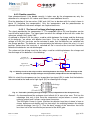
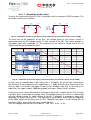
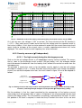
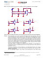
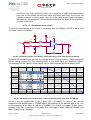
1
Chuo University Studiengang Systemtechnik Vertiefungsrichtung Power and Control Diplom 2007 Dominik Biner Power supply and motion system for planetary rover Dozent Mister Michel Imhasly Experte Dr. Eng. Yasuharu Kunii Tokyo, 20. Februar 2008 Tokyo, February 20th 2008 Chuo University Table of contents 1. General information about planetary rovers___________________________________________6 2. Structure of this diploma work _____________________________________________________6 2.1. Introduction to my work _____________________________________________________________6 2.2. Requirements specification ___________________________________________________________7 2.2.1. Power supply _____________________________________________________________7 2.2.2. Motor speed control________________________________________________________7 2.3. Operating schedule __________________________________________________________________8 3. Analyses and first approaches ______________________________________________________9 3.1. Introduction to this paragraph ________________________________________________________9 3.2. Optimisation of the wheel’s shape______________________________________________________9 3.3. Power supply (Lithium polymer batteries) _____________________________________________10 3.3.1. 3.3.2. 3.3.3. 3.3.4. 3.3.5. 3.3.6. Selection of the batteries ___________________________________________________10 Selection of the charging equipment __________________________________________11 Approach how to use batteries and charging equipment___________________________13 Approach for the generation of the different voltage levels ________________________15 Block diagram of the power supply___________________________________________17 List of required material / elements___________________________________________18 3.4. Motor speed control ________________________________________________________________18 4. Realisation suggestions for the power supply _________________________________________24 4.1. Introduction to this paragraph _______________________________________________________24 4.2. Regulation of the solar cells’ voltage___________________________________________________24 4.3. Voltage levels generation ____________________________________________________________24 4.4. Battery cell voltage control __________________________________________________________25 4.4.1. Measure of the cell voltages / detection of the start of charge ______________________25 4.4.1.1. Simulation of the circuit ______________________________________________36 4.4.2. Other required detections___________________________________________________37 4.4.3. Double securities _________________________________________________________38 4.4.3.1. Too low cell voltage (discharge process) _________________________________38 4.4.3.2. Too high cell voltage (charge process) ___________________________________40 4.4.4. Use of A/D-converters for the cell voltage control _______________________________40 4.4.4.1. How to use the converter MAX197 / description of the device _________________41 4.5. Battery current control _____________________________________________________________46 4.5.1. Current measure with current sensor from LEM_________________________________47 4.5.1.1. Simulation of the circuit ______________________________________________52 4.5.2. Security measures (µP-independent) __________________________________________53 4.5.2.1. Too high current during the discharge process ____________________________53 4.5.2.2. Too high current during the charge process _______________________________55 4.5.3. Current measure with shunt resistance ________________________________________55 4.5.3.1. Use of a differential amplifier __________________________________________55 4.5.3.2. Use of an inverting amplifier __________________________________________61 4.5.3.3. A/D conversion with the MAX197 _______________________________________63 Biner Dominik Diploma thesis Power supply and motion system for planetary rover page 1/78 Tokyo, February 20th 2008 Chuo University 4.5.4. Comparison between the different measuring methods ___________________________63 4.5.5. Detection of the end of charge_______________________________________________64 4.6. Battery temperature control _________________________________________________________64 4.7. Additional battery__________________________________________________________________65 5. Manufacturing of the electronic circuits (PCB) _______________________________________65 5.1.1. Cell voltage measuring circuit_______________________________________________66 5.1.2. Current measuring circuit __________________________________________________67 6. Test of the electronic circuits (PCB) ________________________________________________68 6.1.1. Cell voltage measuring circuit_______________________________________________68 7. Conclusion ____________________________________________________________________68 7.1. Work performed___________________________________________________________________68 7.2. Work to be undertaken / future tasks__________________________________________________69 7.3. Major difficulties encountered during this diploma work _________________________________71 7.3.1. Personal statement ________________________________________________________71 8. Acknowledgments _______________________________________________________________72 9. List of references and other links __________________________________________________73 9.1. References used in paragraph 1 ______________________________________________________73 9.2. Companies/Agencies involved in this project____________________________________________73 9.2.1. Human Machine Systems Laboratory (HMSL)__________________________________73 9.2.2. Japan Aerospace Exploration Agency (JAXA) __________________________________73 9.3. Sources for the choice of LiPos and charging equipment __________________________________74 9.3.1. Company Hyperion _______________________________________________________74 9.3.2. Manuals of charging equipment _____________________________________________74 9.3.3. General information about lithium polymer batteries _____________________________74 9.4. Manufacturers of DC/DC-converter___________________________________________________75 9.4.1. Lambda ________________________________________________________________75 9.4.2. Vicor _________________________________________________________________75 9.4.3. Deutronic _______________________________________________________________76 9.5. Manufacturer of MOSFET drivers (IRF) ______________________________________________77 9.6. Sources for information about MOSFET transistors _____________________________________78 Biner Dominik Diploma thesis Power supply and motion system for planetary rover page 2/78 Tokyo, February 20th 2008 Chuo University Illustration listing Fig. 1 : Sketch of the new wheel placement (use of circular and pentagon-shaped wheels) __________ 9 Fig. 2 : Picture of the charger EOS 1210i________________________________________________ 12 Fig. 3 : Picture of the balancer EOS LBA10 ______________________________________________ 12 Fig. 4 : Discharge curves of a CL-1S 2100mAh with different discharge current values (from Air Craft) 13 Fig. 5 : Scheme of the arrangement possibility of the voltage regulators (case 1) _________________ 15 Fig. 6 : Scheme of the arrangement possibility of the voltage regulators (case 2) _________________ 15 Fig. 7 : Block diagram of the power supply_______________________________________________ 17 Fig. 8 : Electrical scheme of an H-bridge (motor driver for speed regulation)_____________________ 19 Fig. 9 : Simplified scheme of a MOSFET driving circuit _____________________________________ 21 Fig. 10 : Differential amplifier __________________________________________________________ 25 Fig. 11 : Modified differential amplifier (high common-mode voltage) ___________________________ 26 Fig. 12 : Equivalent scheme of the modified amplifier for calculating the input voltage of the OP amp __ 27 Fig. 13 : Equivalent scheme of the modified amplifier for calculating the voltage UR2low______________ 28 Fig. 14 : Electrical schema of the battery cell voltage measuring circuit (with LM324) _______________ 31 Fig. 15 : Electrical schema of the battery cell voltage measuring circuit (with LMV324)______________ 33 Fig. 16 : Simulation schema of the battery cell voltage measuring circuit (with LM324)______________ 36 Fig. 17 : Simulation result of the battery cell voltage measuring circuit (with LM324)________________ 36 Fig. 18 : Driving circuit for the relays used for switching between the charge and the discharge of the batteries (switching through analogue circuit possible, independent of the microprocessor) ___ 38 Fig. 19 : Truth table (switching through analogue circuit, independent of the microprocessor) ________ 38 Fig. 20 : NOT gate realised with a NOR gate ______________________________________________ 39 Fig. 21 : Picture of the A/D converter MAX197 in its simplest operational configuration _____________ 41 Fig. 22 : Table for the selection of the analogue input channel (A/D converter) ____________________ 42 Fig. 23 : Table for the selection of the voltage range of the analogue inputs (A/D converter) _________ 42 Fig. 24 : Table for the determination of the full scale input voltage (A/D converter) _________________ 42 Fig. 25 : Reference-adjust circuit (A/D converter)___________________________________________ 43 Fig. 26 : Relationship between the internal clock period and the external capacitor (A/D converter) ____ 43 Fig. 27 : Table for the selection of the clock mode (A/D converter) _____________________________ 44 Fig. 28 : Table with the complete format of the control byte (A/D converter) ______________________ 45 Fig. 29 : Used control byte for the conversion of the cell voltage value (A/D converter)______________ 45 Fig. 30 : Wiring diagram for the conversion of the cell voltage value (A/D converter) _______________ 45 Fig. 31 : Conversion timing if using internal acquisition mode (A/D converter)_____________________ 46 Fig. 32 : Linear relation between the output voltage and the measured current (LEM LTSR 6-NP) _____ 47 Fig. 33 : Choice of nominal current through different connexion schemes (LEM LTSR 6-NP) _________ 48 Fig. 34 : Electrical schema of the battery current measuring circuit (with LEM LTSR 6-NP) __________ 50 Fig. 35 : Simulation schemes of the battery current measuring circuit (with current sensor (LEM)) _____ 52 Fig. 36 : Simulation result of the battery current measuring circuit (with current sensor (LEM))________ 52 Fig. 37 : Simulation result of the battery current measuring circuit (with current sensor (LEM))________ 53 Fig. 38 : Driving circuit for the relays used for switching between the charge and the discharge of the batteries (switching through analogue circuits possible (µP-independent)) (faulty) ___________ 53 Biner Dominik Diploma thesis Power supply and motion system for planetary rover page 3/78 Tokyo, February 20th 2008 Chuo University Fig. 39 : Truth table of the RS latch M74HC279____________________________________________ 54 Fig. 40 : Driving circuit for the relays used for switching between the charge and the discharge of the batteries (switching through analogue circuits possible (µP-independent)) (final version) _____ 54 Fig. 41 : Truth table (switching through analogue circuit, independent of the microprocessor) ________ 54 Fig. 42 : Differential amplifier with low-pass RC filter ________________________________________ 57 Fig. 43 : Electrical schema of the battery current measuring circuit (with shunt and LM324) __________ 58 Fig. 44 : Electrical schema of the battery current measuring circuit (with shunt and rail-to-rail amplifier)_ 59 Fig. 45 : Simulation schema of the battery current measuring circuit (with shunt and LM324)_________ 60 Fig. 46 : Simulation result of the battery current measuring circuit (with shunt and LM324)___________ 60 Fig. 47 : Differential amplifier with low-pass RC filter ________________________________________ 61 Fig. 48 : Simulation schema of the battery current measuring circuit (with shunt and LM324)_________ 62 Fig. 49 : Simulation result of the battery current measuring circuit (with shunt and LM324)___________ 63 Fig. 50 : Used control byte for the conversion of the current value measured with a shunt resistance (A/D converter) __________________________________________________________________ 63 Fig. 51 : Picture of the first version of the cell voltage measuring circuit (PCB) ____________________ 66 Fig. 52 : Picture of the second version of the cell voltage measuring circuit (PCB) _________________ 66 Fig. 53 : Connexion diagrams of the LM324 (left) and the LM339 (right) _________________________ 67 Fig. 54 : Pictures of the populated cell voltage measuring circuit _______________________________ 67 Fig. 55 : Pictures of the test setup for the cell voltage measuring circuit _________________________ 68 Biner Dominik Diploma thesis Power supply and motion system for planetary rover page 4/78 Tokyo, February 20th 2008 Chuo University List of appendices The appendices are placed at the end of this report. All the datasheets of electronic devices are available as PDF-files on the enclosed CD (appendix 5). 1. Study results about the wheel form done by Kojiro Iizuka, Yoshinori Sato, Yoji Kuroda and Takashi Kubota (1a and 1b) 2. Extract from the Hyperion product catalogue 3. List of material bought for making the first battery charge/discharge tests 4. Test record of the cell voltage measuring circuit 5. CD with the datasheets of electronic devices 5a) 12V DC-motor from Maxon (A-max 26) with gear & encoder 5b) 12V DC-motor from Maxon (A-max 19) with gear & encoder 5c) Charging unit 1210i from Hyperion (user manual) 5d) Balancer LBA10 from Hyperion (user manual) 5e) MOSFET transistor K2936 5f) Operational amplifier LMV324 5g) Comparator LMV339 5h) Operational amplifier LM324 5i) Comparator LM339 5j) Quad 2-input NOR gate M74HC02 5k) Relay from the company Finder (Series 66) 5l) Relay from the company Omron (LY2) 5m) A/D-converter MAX197 5n) Current sensor LTSR 6-NP (LEM) 5o) Quad RS latch 74HC279 5p) Quad 2-input AND gate MM74HC08 5q) Temperature sensor LM35 Biner Dominik Diploma thesis Power supply and motion system for planetary rover page 5/78 Tokyo, February 20th 2008 Chuo University 1. General information about planetary rovers Nowadays robots are used to explore planets in our solar system. They are one of the most important mission devices for planetary explorations [1]. The environment on these planets is not well known and therefore it’s necessary that a robot can get and treat this information on its own. If the rover is able to get steadily new data over its environment, it can adjust the path on its own and correct its position information and therefore eliminate long breaks while driving to a waypoint. Else breaks are caused by the transmission delay of required orders from the control station on earth. Several approaches to this problem were made. Almost all of them are based on distance maps produced by stereo vision systems or laser range finder [2], [3]. Another issue is the motion control of the rover. There are different problems which can occur while driving on planetary surfaces, such as slipping of wheels which induces additional errors to the position information of the rover or worst, if the rover gets stuck. Some studies done before by the Chuo University in Tokyo show, that especially if the rover has to overcome rough terrain and slopes, the shape of the wheels has much influence on the rover’s mobility. Also the weight of the rover has to be as low as possible to decrease costs and the probability of getting stuck. An actively articulated suspension is essential, because it can greatly improve the rover’s stability in rough terrain [1], [3]. At the moment the Human Machine Systems Laboratory (HMSL) at Chuo University in Tokyo is developing a new rover type called M6. It will be used to explore the poles of the moon. For the M6, the complete system has to be composed, including a battery with a power source for charging it. Only the mechanical design is done by other institutions. The power supply is realised with lithium polymer batteries and solar cells. The development of the solar cells is carried out by JAXA1. Lithium polymer batteries are quite sensitive to temperature and over- or undervoltage. Furthermore, the balance between the different cells has to be granted in order to guaranty a good battery performance and a long battery life. This means that after charging, all cells have to be at the same voltage. Thus it needs provisions for keeping them in a safe and appropriate condition [3]. For contact information concerning the HMSL and JAXA see chapter 9.2. The references used for writing this paragraph are listed in chapter 9.1. 2. Structure of this diploma work 2.1. Introduction to my work The development of the power supply for the new type of planetary rover (M6) is my main work here in Japan (Chuo University, Korakuen Campus). This work is linked to the speed regulation of the motors used for the motion control of the rover. On this account I also help to develop a method for realising the speed regulation. Besides, depending on the available time, I help Dr. Eng. Kojiro Iizuka with the optimisation of the wheel’s shape. As mentioned before, the development of the solar cells isn’t done by Chuo University. In the first instance, my work consists of setting up concepts and to define possible approaches. The final realisation of the circuits has to be done by a laboratory with the appropriate infrastructure. 1 JAXA = Japan Aerospace Exploration Agency. Biner Dominik Diploma thesis Power supply and motion system for planetary rover page 6/78 Tokyo, February 20th 2008 Chuo University 2.2. Requirements specification 2.2.1. Power supply As aforementioned, the necessary electrical power has to be delivered by lithium polymer battery cells (LiPos). Following conditions have to be kept: • • • • • • Capability to deliver a current of 10 A continuously Generation of 5, 12 and 24Vdc (without DC/DC-converters) Autonomy of 2 hours, with a consumption of 300 W/h Availability of an emergency shut-down Maximal dimensions of one battery unit is 88mm x 175mm x 50mm Charging of the batteries with a current of 1C2. The most important thing is to keep the batteries in a safe and appropriate condition. This means: • Temperature of each battery pack between 0°C and 60°C • Balance between each cell of a battery pack (all cells same voltage) • Protection against over- and undervoltage (cell voltage within 3V and 4.2V) • Appropriate charge and discharge of the battery packs • Control of the battery current If the temperature of a battery pack exceeds 60°C, it’s going to explode (development of vapour inside the battery pack). If the temperature falls under 0°C, the cell will be damaged and losses of capacity will occur. Capacity losses will also take place if the cell voltage goes beyond the abovementioned limits. The operating temperature of the battery packs is at about 50°C. 2.2.2. Motor speed control For the motion and the steering of the rover, 12V DC-motors from Maxon are deployed (Amax series). They are equipped with a planetary gear and an encoder. The type of motors along with the gear and the encoder has already been chosen before (the datasheets are on the enclosed CD (appendix 5a and 5b)). The type with 11 watts (appendix 5a) is used for the motion of the rover and the smaller one for the steering. Normally a first adaptation of the voltage is realised with DC/DC-converters, but in this case they are too big and cause too many losses. The average supply voltage of the motor, which determines the motor speed, has to be generated directly from the battery voltage. Remark: The requirements specification has been written by myself. For it I used information about LiPos gathered during the summer vacation before coming to Japan as well as the information get through discussions with my person in charge Dr. Eng. Yasuharu Kunii. Unfortunately I didn’t take notes of the sources used during the summer vacation. 2 With lithium polymer batteries the current is mostly given by a multiple of their capacity. For example with a 2.7Ah battery, 1C correspond to a current of 2.7 amperes, 2C would be 5.4 amperes and so on. Biner Dominik Diploma thesis Power supply and motion system for planetary rover page 7/78 Tokyo, February 20th 2008 Chuo University 2.3. Operating schedule Besides the diploma work, I have to follow Japanese language lessons at the Tama Campus of Chuo University. Until the winter vacation I have seven lessons per week, from Wednesday to Friday. Therefore during this period I’m only working two days a week on this project. Additionally, every Thursday afternoon I lead an English lesson for Japanese students, also at the Tama Campus. But due to the limited time, after November 5th I don’t give these lessons anymore. Biner Dominik Diploma thesis Power supply and motion system for planetary rover page 8/78 Tokyo, February 20th 2008 Chuo University 3. Analyses and first approaches 3.1. Introduction to this paragraph Because many things are unknown or not defined yet, only possible approaches are described in this paragraph. More detailed realisation suggestions for the different parts will be treated in chapter 4. This section is also used for the first description of the approaches to my person in charge in Japan (Dr. Eng. Yasuharu Kunii) and serves as help for the following realisation. 3.2. Optimisation of the wheel’s shape First of all I read the study results about the wheel form done by Kojiro Iizuka, Yoshinori Sato, Yoji Kuroda and Takashi Kubota (see appendix 1). I concluded that the effects of hardening soil and shearing stress (low slip ratio) are the most important. So the aim is to combine these two effects as good as possible. How it can be seen in figure 11 of appendix 1a and table 2 of appendix 1b, the elastic wheel as well as the pentagon and the combined wheel types provoke a hardening of the soil. But the slip ratio for the pentagon typed wheel is relatively high (see fig. 12, appendix 1b). In contrast the combined types (pentagon / circular wheel with lugs) and the elastic wheel combine the two effects fairly well. But the elastic wheel tends to be deformed by the charge and thus this type can not be used. In my opinion the combined wheels (see fig. 6, appendix 1b) are expensive to manufacture. So the idea is to use a pentagon typed wheel for hardening and a circular wheel with lugs, in series to the aforementioned wheel, to create the shearing effect (see picture below). By means of the actively articulated suspension the charge given on each wheel can be controlled and thus optimise the effect of each wheel. Due to the limited time and that the development of the power supply as well as the speed regulation of the motors have a higher priority, this approach has to be analysed by Dr. Eng. Kojiro Iizuka. The experimental system (see fig. 8&9 of appendix 1b) has to be adapted, as this system is only for tests with one wheel. Wheels 1 1 1: Pentagon typed wheels 2 2 1 1 2: Circular wheels with lugs Fig. 1 : Sketch of the new wheel placement (use of circular and pentagon-shaped wheels) Biner Dominik Diploma thesis Power supply and motion system for planetary rover page 9/78 Tokyo, February 20th 2008 Chuo University 3.3. Power supply (Lithium polymer batteries) The charging of lithium polymer batteries (LiPos) is delicate. The charging has to be done with constant power and the voltage of each cell has to be within the range of 3.0V and 4.2V. After charging, the voltage of all cells in the pack has to be the same (balance between the cells). For these reasons, it would be a great advantage to be able to use products already on the market for charging the batteries safely. Of course the temperature has to be within the allowed limits at all times. The batteries, as well as the charging equipment, are chosen from the product range of the company Hyperion. Hyperion is a provider of R/C products and offers quality components at a reasonable price. For contact information of Hyperion, information about the charging equipment and general sources about LiPos see chapter 9.3. 3.3.1. Selection of the batteries The nominal voltage of a lithium polymer battery cell is 3.7V. During the discharge of a battery pack, the cell voltage drops. The power supply will be dimensioned so that the discharge will be stopped when the voltage of one cell reaches about 3V. Therefore it needs 8 cells connected in series to generate the required 24V. The highest amount of battery cells in one pack is only six. Therefore it needs two packs connected in series to reach the demanded voltage. To be able to use only one battery charger for charging two packs at the same time, the packs have to be identical. Thus battery packs with 4 cells (4S-type) will be used. In order to increase the autonomy time of the rover, as much capacity as possible is needed. As a result, following battery packs would be suitable: - Hyperion CL - 4S 4800mAh, 96.0A Continuous (20C) Weight: 515gr, Size: 44 x 150 x 40 mm - Hyperion CL - 4S 4200mAh, 67.2A Continuous, (2100-2P 16-22C) Weight: 384gr, Size: 34 x 102 x 51 mm Remark: There are two series of battery packs provided by Hyperion, the VX LiPo packs (blue series) and the CL LiPo packs (red series). In our case it’s better to use batteries from the red series (CL stays for capacity and low weight (light)). For more information see the extract from the Hyperion product catalogue attached to this report (appendix 2). In order to reach an autonomy time of about 2 hours, the total available capacity has to be 20Ah: Pused = 300W ; U nominal = 30V ; t autonomy = 2h ⇒ Wused = Wneeded = Pused ⋅ t autonomy = 600Wh Q needed ≡ needed capacity; ⇒ Q needed = Wneeded = Q needed ⋅U nominal Wneeded = 20 Ah U nominal Therefore it needs at least 4 units of 2x4S-packs, so overall 8 battery packs. Therewith we Biner Dominik Diploma thesis Power supply and motion system for planetary rover page 10/78 Tokyo, February 20th 2008 Chuo University reach a total capacity of 16.8 Ah and 19.2 Ah with the 4800mAh type respectively. As it can be seen, the difference in weight is quite high compared to the difference in capacity. The 4800mAh type has a capacity/weight ratio of 9.3mAh per gram, the other one 10.9mAh per gram. But if we analyse the difference it brings in energy (see below), it’s definitely better to use batteries with a capacity of 4800mAh. - 260gr difference => totally 1.04 kg more weight of the rover - Speed of the rover is 0.1 m/s => Wdiff = 1 - Speed of the rover is 0.2 m/s => Wdiff = 1 2 ⋅ m ⋅ v 2 = 5.2mJ 2 ⋅ m ⋅ v 2 = 20.8mJ - 0.6Ah difference => totally 2.4 Ah more capacity, so Wdiff = Qdiff ⋅ U nominal = 72 J As aforementioned with the 4800mAh type the total available capacity is 19.2 Ah, which affords an autonomy time of 1 hour and 55 minutes. To augment this time, more than 4 units are necessary. But the batteries are mounted under the body of the rover and there is not more space available. Thus additional units would have to be placed somewhere else, for example laterally, in front or at the rear of the rover. One battery unit consists of two battery packs and the maximal allowed dimension of one unit is 88mm x 175mm x 50mm (see requirements specification in chapter 2.2.1). The dimension of each pack is 44mm x 150mm x 40mm and they are placed abreast. Thus one battery unit is 88mm x 150mm x 40mm big, which is within the given limits. The batteries can deliver a current up to 96 amperes (20C) which is completely sufficient. For charging the batteries with a current of 1C, thus 4.8 ampere, it needs about 150 watt of power for each pair of battery pack. Therefore for charging all battery units at the same time 600 watts are required. 3.3.2. Selection of the charging equipment For charging the lithium polymer batteries, the charger EOS 1210i is deployed. It allows charging battery packs with up to 12 cells. It charges the battery with constant power and stops automatically when the batteries are full (cell voltage at 4.2V). The maximum power delivered by this charging unit is 180W. This is enough to charge the batteries like demanded. Due to this power limitation, the maximal current which can be delivered in our case is 7.5 amperes (when each cell is at 3V). Of course this value depends of the power given by the solar cells, which are used to supply the charger. The supply voltage of the charger has to be constant and between 12V and 15V. Therefore a voltage regulation of the output voltage of the solar cells is required (see chapter 4.2). There is also a temperature sensor available for this charger, which allows monitoring the temperature of the battery packs on the charger’s LCD-Display. Moreover the temperature at which the charger should stop to charge can be set between 10°C to 55°C. As we have 4 times 2x4S-packs, we need four chargers. Biner Dominik Diploma thesis Power supply and motion system for planetary rover page 11/78 Tokyo, February 20th 2008 Chuo University Fig. 2 : Picture of the charger EOS 1210i Remark: The start of charge can not be done automatically. Some buttons of the chargers have to be pressed manually. There are no chargers on the market which allow starting the charge without a manual command, because the charge of lithium polymer batteries should not be unattended. Therefore the charger will have to be modified. This means that the corresponding buttons have to be replaced by bipolar transistors, which can be driven by the microprocessor. Due to the missing time, the infrastructure and the missing specialists in this domain, the development of a charger during this diploma work is not possible. Moreover it would most likely be more expensive as the charger mentioned above. But it could be realised more space saving. Anyway, to make the first tests, the necessary equipment to charge one battery unit (two 4-cells packs in series) is already ordered (see appendix 3). To balance the cells, the balancer EOS LBA10 is used. It is compatible with the charger mentioned above and gives the possibility to monitor the battery voltage on the charger’s display. With it up to 6 cells can be balanced while or after charging. Thus in our case we need to connect two of them together to be able to balance the 8 cells. So overall we need 8 balancers. Fig. 3 : Picture of the balancer EOS LBA10 For more information about the charger and the balancer, see the extract from the Hyperion product catalogue attached to this report (appendix 2) as well as the user manuals on the enclosed CD (appendices 5c & 5d). Biner Dominik Diploma thesis Power supply and motion system for planetary rover page 12/78 Tokyo, February 20th 2008 Chuo University 3.3.3. Approach how to use batteries and charging equipment Now it has to be defined how the material is going to be used. First of all some definitions: - A battery unit consists of two 4S 4800mAh battery packs connected in series - Overall there are four battery units - After charging/balancing the balancer has to be disconnected from the battery, because it puts an extremely small drain on the battery (≈ 0.5mA) and it prevents the discharge of the batteries. The idea is to always use two battery units together in parallel, because so the current drawn is distributed on the two units. The advantage of the current distribution is that there will be less heat creation in each pack and as the current is smaller, the capacity of the battery packs can certainly fully be used (see graph below). Furthermore during the discharge of one pair of battery units, the other one can be charged. As it can be seen in the graph below, when using the batteries with a small current the cell voltage changes much more as with a high current. With a high current the cell voltage stays more or less constant during most of the discharge time. But this doesn’t cause any problem in our application, as the battery voltage is regulated. Fig. 4 : Discharge curves of a CL-1S 2100mAh with different discharge current values (from Air Craft) Of course if all the units would be used together, the current drawn from each unit would be divided by four. But then all the batteries will be empty at the same time and at this point the rover is obliged to stop his work for charging them. Thus, to avoid this case, under no circumstances all four units are discharged at the same time, but of course the four units can be charged at the same time. The switching between the two pairs of battery units takes place when one of them is empty and has to be charged. If at this point the other pair has to be charged too, it’s connected to the consumer depending on its charge-level, even if it’s not fully charged. To realize the switching, following detections are needed: Biner Dominik Diploma thesis Power supply and motion system for planetary rover page 13/78 Tokyo, February 20th 2008 Chuo University 1. start of charge: For detecting when the batteries have to be charged, a voltage measure is necessary. As soon as the voltage of one cell reaches 3.0V to 3.2V, it means that the battery is empty. The voltage value is depending on how much current is drawn from the battery (see fig. 4). There are different ways for measuring this voltage, depending on how the packs, in series or parallel, are discharged. If the voltage of each cell decreases at the same level, it’s sufficient to measure the voltage of one battery pack or even of one battery unit. Else it’s necessary to control the voltage of each cell. To get the cell’s voltage, either the signals on the balance harnesses of the balancer are used, or a cell voltage measuring system has to be installed. Action done: - Connect other two units to the consumer (depending on their charge-level). - Interrupt existent connexion to the load. - Supply the appropriate chargers and balancers and connect them with the empty units. 2. end of charge: The detection of the end of charge (Ucell = 4.2V) is done automatically by the charger. The balancer is shut down, but as abovementioned it has to be disconnected from the batteries. This point will be detected by a measure of the current drawn from the batteries by the balancer, which at this time is only about 0.5mA. The connexion to the load is done when the other two units are discharged. Action done: - Take away the power supply of the appropriate chargers and balancers. At any time the temperature as well as the current has to be controlled. While charging, the control of the temperature can be realised by means of the charging unit 1210i with the corresponding temperature sensor. During the discharge of the batteries, it has to be done by the logical unit (for example a microprocessor), which also takes care of the above described actions and therefore controls all the process. This control unit gets the necessary information from different sensors and from measuring circuits respectively. Thus for the measure of the temperature during the discharge, either the sensor of the charger will be used, or if it’s not possible, another sensor has to be installed. The current is measured with a current sensor from the company LEM. The current value is transmitted to the control unit, so that it knows what happens and can decide what to do. Some detection can be realised by means of analogue circuits which only transmit a logical signal to the control unit. For example at the end of the charge the logical unit gets the order to disconnect the chargers and balancers by a logical signal (0V or 5V). Anyway, the values of the current and the temperature have to be transmitted to the control unit, so that if any value exceeds the nominal rate, it can react before they reach critical values. Moreover if an error occurs, it can be dedicated what happened before. Biner Dominik Diploma thesis Power supply and motion system for planetary rover page 14/78 Tokyo, February 20th 2008 Chuo University For the cell voltage measure, required for detecting the start of charge and determinate the charge level of the batteries, either an analogue input of the processor is used, or an accordant logical signal is generated. Instead of analogue inputs, external A/D-converters can be deployed. The detection of critical values of cell voltage, battery current or battery temperature can be realised by analogue circuits which directly act by themselves, without the use of the microprocessor. For example when the discharge current exceeds a certain value, the batteries are directly disconnected from the load by the analogue circuits. 3.3.4. Approach for the generation of the different voltage levels To generate the different voltage levels (5V, 12V and 24V) from the battery voltage, standard voltage regulators could be used. They cause many losses and therefore it’s better to use DC/DC-converters, but in the first instance my person in charge, Professor Kunii, doesn’t want to use them. So this point has to be discussed (further see chapter 4.3). To choose the power class of each regulator, we need to know the consumption for each level. Depending of the power consumption of each level, it has to be determined whether it’s better to use the battery voltage or the output of the 24V-regulator as input voltage for the 12V-regulator (see pictures below). In the latter case (fig. 6) all the power is given by the 24V-regulator and of course the total amount of losses stays unchanged, but therefore the other regulators dissipate less power. In other words, the distribution of the power on each regulator can be chosen (also see examples after fig. 6). 1st case: 24V Voltage regulator Ubatteries 12V Voltage regulator +24Vdc 30Vdc +12Vdc 5V Voltage regulator +5Vdc Fig. 5 : Scheme of the arrangement possibility of the voltage regulators (case 1) 2nd case: 24V Voltage regulator Ubatteries 12V Voltage regulator +24Vdc 30Vdc +12Vdc 5V Voltage regulator +5Vdc Fig. 6 : Scheme of the arrangement possibility of the voltage regulators (case 2) Biner Dominik Diploma thesis Power supply and motion system for planetary rover page 15/78 Tokyo, February 20th 2008 Chuo University Here two examples to explain this conclusion: U out 12V−regulator = 12V ; f .ex. : I out 12V − regulator = 2 A; ⇒ U out 24V−regulator = 24V ; I out 24V − regulator = 5 A; 1st case : U in 12V − regulator = U in 24V − regulator = U available ⇒ Wused 12V − regulator = (U in 12V − regulator − U out 12V − regulator ) ⋅ I out 12V − regulator = 36 W ⇒ Wused 24V − regulator = (U in 24V − regulator − U out 24 V − regulator ) ⋅ I out 24 V − regulator = 30 W ⇒ Wused total =Wused 12V − regulator + Wused 24V − regulator = 66 W 2 nd case : U in 12V − regulator = U out 24V − regulator ; U in 24V − regulator = U available ⇒ Wused 12V − regulator = (U in 12V − regulator − U out 12V − regulator ) ⋅ I out 12V − regulator = 24 W ⇒ Wused 24V − regulator = (U in 24V − regulator − U out 24 V − regulator ) ⋅ ( I out 24 V − regulator + I out 12V − regulator ) = 42 W ⇒ Wused total =Wused 12V − regulator + Wused 24V − regulator = 66 W f .ex. : I out 12V − regulator = 5 A; ⇒ U available = 30V ; I out 24V − regulator = 2 A; 1st case : U in 12V − regulator = U in 24V − regulator = U available ⇒ Wused 12V − regulator = (U in 12V − regulator − U out 12V − regulator ) ⋅ I out 12V − regulator = 90 W ⇒ Wused 24V − regulator = (U in 24V − regulator − U out 24 V − regulator ) ⋅ I out 24 V − regulator = 12 W ⇒ Wused total =Wused 12V − regulator + Wused 24V − regulator = 102 W 2 nd case : U in 12V − regulator = U out 24V − regulator ; U in 24V − regulator = U available ⇒ Wused 12V − regulator = (U in 12V − regulator − U out 12V − regulator ) ⋅ I out 12V − regulator = 60 W ⇒ Wused 24V − regulator = (U in 24V − regulator − U out 24 V − regulator ) ⋅ ( I out 24 V − regulator + I out 12V − regulator ) = 42 W ⇒ Wused total =Wused 12V − regulator + Wused 24V − regulator = 102 W Remark: For the calculation of the losses for the second case, the output currents of both regulators have been summed. Of course it’s the input current of the 12V-regulator that is added to the output current of the 24V-regulator (see fig. 6). But the input and the output current of the 12V-regulator have the same value. As it can be seen, by using voltage regulators for the generation of the different voltage levels, the efficiency is very bad, especially when the 12V-regulator has to deliver much current. For the first example the total efficiency is only 68.6% (Pin = 210W, Pout = 144W) and for the second example only 51.4% (Pin = 210W, Pout = 108W). Biner Dominik Diploma thesis Power supply and motion system for planetary rover page 16/78 Tokyo, February 20th 2008 Chuo University 3.3.5. Block diagram of the power supply The values (voltage, current and power) are given for charging the batteries with maximal possible current. This means that every charger consumes 180 watts. + voltage regulation U = [24, 33.6] V I = [5.4, 7.5] A P = 180 W U = [12, 15] V I = [24, 30] A P = 360 W U = [12, 15] V I = [48, 60] A P = 720 W 1 2 + charger 1210i - - 1 + charger 1210i - Solar Cells ??Vdc 1 2 + charger 1210i - 2 + charger 1210i + + - balancer LBA10 Slave + + - - Lithium Polymer battery pack 4 cells, 4.8 Ah network cable + 1 - balancer LBA10 Master 30Vdc 4.8 Ah + + - - Lithium Polymer battery pack 4 cells, 4.8 Ah + + - balancer LBA10 Slave + + - - Lithium Polymer battery pack 4 cells, 4.8 Ah network cable + - balancer LBA10 Master 30Vdc 4.8 Ah + + - - Lithium Polymer battery pack 4 cells, 4.8 Ah - Fig. 7 : Block diagram of the power supply Remark: The two 30Vdc outputs are connected together in parallel. Therefore the capacity adds up to 9.6 Ah. These outputs represent the input for the voltage level generation (Ubatteries in fig. 5 and fig. 6). The lower part with the 4 balancers and the 4 battery packs, is required a second time for the other pair of chargers ( 2 ). Biner Dominik Diploma thesis Power supply and motion system for planetary rover page 17/78 Tokyo, February 20th 2008 Chuo University 3.3.6. List of required material / elements For realising the abovementioned approaches it needs following components: • 8 lithium polymer battery packs with 4 cells and 4.8Ah each • 4 chargers 1210i with 4 temperature sensors • 8 balancers LBA10 with the appending cables: o 8 times the balance harnesses for 4S batteries o 4 network cable/adapter sets for connecting two balancers together • 8 relays, with 2 change-over3 contacts each, for switching between the charge and the discharge of the batteries as well as 8 bipolar transistors to drive the relay’s coils (the transistors can be switched by the microprocessor) • 2 power MOSFET transistors for connect/disconnect the power supply of the chargers. To be able to choose which two units are used together in parallel (not implicitly always the same two together), 4 power MOSFET transistors are necessary, in order that the power supply of each charger can individually be connected or disconnected. • 4 current sensors for controlling the current drawn or delivered by each battery unit or 8 if the batteries are not in series during the charge process, in order to measure the current of each battery pack. Or shunt resistors; either 4 (or 8) for measuring the charge current and 4 for measuring the discharge current, or only 4 (or 8) if both current senses are measured with the same resistance (positive and negative voltage on shunt resistor) • A cell voltage measurement and monitoring system • A temperature measurement and surveillance system • A microprocessor as control unit • A powerful voltage regulation (up to 720W) for generating the supply voltage for the chargers from the solar cells (DC/DC converter) • DC-DC-converters and/or voltage regulators for the generation of the different voltage levels (5V, 12V and 24V) 3.4. Motor speed control As mentioned in chapter 2.2.2, the 12Vdc motors have to be driven directly with the battery voltage. Depending of the charge level of the battery, the voltage varies between 24Vdc and 33.6Vdc. For the regulation of the motor speed, an H-bridge will be used as motor driver (see figure below (fig. 8)). Therewith the motor can be actuated directly with 24Vdc to 33.6Vdc, without the need of a very high or low duty cycle of the PWM4 signal. Moreover, a part of the motor current flows back into the battery. Therefore in average less current is drawn and hence less of the battery’s capacity used. 3 4 Change-over or double-throw contact, also called “transfer” contact means: one normally-open contact and one normally-closed contact with a common terminal. PWM = Pulse Width Modulation. A PWM signal represent a rectangular signal where the duty cycle is changed like needed. With an H-bridge used like described above, with a duty cycle of 50%, thus a normal rectangular signal, the motor stands still. With 50% to 100% the speed increases in one direction, with 50% to 0% in the other direction. Biner Dominik Diploma thesis Power supply and motion system for planetary rover page 18/78 Tokyo, February 20th 2008 Chuo University The duty-cycle is calculated as follows: Ton U DCmotor = U batt ⋅ (2m − 1); m = = duty cycle; T U + U batt ⇒ m = DCmotor 2 ⋅ U batt S1 T = period of PWM - signal = Ton + Ton forward : 1a (U batt = 24V ; U DCmotor = 12V ) 1b (U batt = 33.6V ; U DCmotor = 12V ) backward : 2a (U batt = 24V ; U DCmotor = −12V ) 2b (U batt = 33.6V ; U DCmotor = −12V ) S1 ⇒ m = 0.75 ⇒ m = 0.68 ⇒ m = 0.25 ⇒ m = 0.32 S3 Remark: As it can be seen, for moving forward the duty cycle changes only between 50% (stand still) and 75% (full speed). And thus for the other direction of rotation it changes only between 50% and 25%. This is true for the case that T = TonS1+TonS3, this means that the PWM signal is applied as shown in the figure below (fig. 8). The necessary duty cycle to reach the desired motor speed is determined by measuring the motor speed. Ubatt 2 2 Ubatt PWM S3 1 D1 PWM D3 DC-Motor S2 S4 PWM S4 D2 PWM D4 1 S2 1 S1 S3 2 DC-Motor 2 1 S1 Fig. 8 : Electrical scheme of an H-bridge (motor driver for speed regulation) As switches MOSFET transistors are deployed. The realisation of this circuit is done by another student of this laboratory, by Shimanuki Toru. This paragraph serves to give him some first information about the circuit and about the switching of MOSFET transistors, because this is not part of his major subject. Therefore I will continue to assist him in case of questions or problems and help him with the choice of components. Moreover I help him with the performance of tests, but the results are not documented in this report. The most important thing is to ensure that never both transistors of one side are switched on at the same time, because this would short-circuit the battery. Therefore after the transistors S1 and S4 have been switched off and the PWM-signal goes low respectively, a certain amount of time, the so-called dead time, has to be awaited before turning on the other two transistors S2 and S3, to assure that S1 and S4 are completely open. The same is necessary for the following switching of S1 and S4. This time depends of the total gate charge of the MOSFETs and the current available for switching the transistors. Biner Dominik Diploma thesis Power supply and motion system for planetary rover page 19/78 Tokyo, February 20th 2008 Chuo University The necessary switching time can be calculated as follows: t= QG ; IG with I G as gate current QG = QGS + QGD as the total charge at the gate t is the on/off time (t on or t off ) Remark: The total gate charge QG depends of the drain-source voltage, thus of the supply voltage of the H-bridge which in our case correspond to the battery voltage. Moreover the drive resistance in series to the gate has also influence on the switching operation, because together with the input capacity Ciss of the MOSFET, it represents an RCelement. The time constant τ of this RC-element determines how fast the control voltage UGS reaches its final value. UGS has a direct influence on the resistance between drain and source, RDS(on). For switching the transistor on, the input capacity Ciss has to be charged; and discharged when switching off. In fact, while switching the MOSFET on, the capacity CGS is charged by a positive gate current (flows into the gate) and the capacity CGD, which at this moment is charged at the supply voltage of the H-bridge, has to be discharged with a current of the same polarity. While switching off, this process is inverted and consequently a negative gate current is necessary. switch on : U GS (t ) = U GS final t − τ ⋅ 1 − e ; τ = RGate ⋅ Ciss ; Ciss = CGS + CGD switch on switch off switch off : U GS (t ) = U GS − final t ⋅ e ; τ = RGate ⋅ Ciss ; Ciss = CGS + CGD τ Remark: The calculation with the exponential charge or discharge is only rudimental true, because as soon as the gate source voltage UGS reaches the threshold voltage UTh and the transistor enters the active zone, the capacity CGS is increased dynamically by the Miller effect. Especially when UGS reaches the same value as the drain source voltage UDS the capacity is maximal and UGS flattens. But at this point the MOSFET is already nearly fully switched on. Therefore the drive resistance RGate should be small and the gate current high, in order to allow a fast charge and discharge of the gate capacities. To minimise the losses due to the Biner Dominik Diploma thesis Power supply and motion system for planetary rover page 20/78 Tokyo, February 20th 2008 Chuo University switching, the commutation has to be done as fast as possible. But to switch to fast could introduce some EMC (electromagnetic compatibility) problems, therefore in general a small drive resistance is put in series to the gate. The switching of the transistors is realised by MOSFET drivers available on the market. For example the company IRF is producing such drivers. As mentioned before, as longer the switching time, as higher are the losses due to the switching. Therefore the current given by the driver have to be high enough and his internal resistance small enough. The required gate voltage for the upper transistors S1 and S3 depends of the voltage of the source, because their source is not connected to ground and thus not on a 0V potential. Thus the driving circuit for these transistors have to be related to the source, this means the driving circuit follows the source voltage. The picture below shows the simplified scheme of such a driving circuit. Fig. 9 : Simplified scheme of a MOSFET driving circuit The capacitor C1 is charged when M2 is closed (bootstrap circuit). This capacitor provides the necessary energy for the switching of M1. Therefore always the lower transistors (S2 or S4 in figure 8) have to be turned on at first. The gate-source voltage of the upper MOSFET is exclusively determined by the supply voltage of the driver, in this case 15V. The source potential of M1 is irrelevant. Of course the signal for driving M1 has to be provided by a level shifter circuit. Such circuits use charge pumps to create a higher voltage as the supply voltage, which is necessary for switching the upper MOSFETs. A level shifter circuit is already implemented in common driving circuits (e.g. drivers from IRF). Moreover many MOSFET drivers have an undervoltage protection (also called undervoltage lockout protection (UVLO)). This protects the application in the event of a low supply voltage by switching off the MOSFET transistors. For contact information of the company IRF as well as links to general information about MOSFET transistors and their switching see chapter 9.6. The motors used for the steering of the motor have to stand still most of the time and draw a very small current (Inom = 0.2A). Therefore for the speed regulation of these motors, it’s easier to actuate the H-bridge differently (use of the bridge as a buck-converter). This means that the PWM signal is only applied to the upper transistors (S1 and S3). The lower transistors S2 or S4 are permanently switched on. For example for moving forward, the switch S4 is continuously closed and the PWM signal is applied to S1. The transistors S2 and S3 are not used and stay switched off. But like before, after opening S1 and after awaiting the dead time, the transistor S2 can be switched on for reducing the losses due to the diode. In this case the duty-cycle is calculated as follows: Biner Dominik Diploma thesis Power supply and motion system for planetary rover page 21/78 Tokyo, February 20th 2008 Chuo University U DCmotor = U batt ⋅ m; Ton m= S1 or Ton S3 T T U m = DCmotor U batt ⇒ = duty cycle; T = period of PWM - signal a) (U batt = 24V ; U DCmotor = 12V ) ⇒ m = 0.50 b) (U batt = 33.6V ; U DCmotor = 12V ) ⇒ m = 0.36 Remark: In this case the duty cycle for moving forward is the same as for the other direction. The duty cycle changes between 0% (stand still) and 50% (full speed). Calculation of the losses due to the MOSFETs: The following description is for the case that the PWM signal is applied as shown in figure 8 and when the motor is used to move forward. This means that in the scheme (fig. 8) the current flows from left to right through the motor. In case of a rotation in the other side, the principle is the same. As soon as the transistors S1 and S4 are switched off (PWM low), the current has to continue to flow in the same direction. Thus during the dead time the current flows through the diodes D2 and D3 and into the battery. After the dead time S2 and S3 are closed, to reduce the losses due to the diodes. The losses during the conduction are calculated as follows: 1. during PWM high time (losses of S1 & S4) : Ploss channel = RDS ( on ) 2 ⋅ I rms ; Ton T with I rms = I motor ⋅ 2. during PWM low time (losses of S2 and S3) 2a) during dead time (S1 to S4 switched off) : Ploss =UF ⋅ I avg ; with I avg = I motor ⋅ Toff' T 2b) after dead time (S2 & S3 switched on) : Ploss diode diode channel = RDS ( on ) ⋅I 2 rms ; with I rms = I motor ⋅ Toff − Toff' T Remark: The formulas are for the case that the current flowing through the corresponding transistors is a rectangular signal (constant motor current). Ton represent the high time of the PWM-signal, Toff the low time. For the calculation of the losses during the low time of the PWM-signal, the value of the average current Iavg as well as the value of the root mean square current Irms depends on how long the MOSFETs S2 and S3 are switched off (T’off). This means how long the current flows through the diode instead of through the channel. Therefore it depends on the dead time. As the dead time is awaited before closing S2 and S3 and again before closing S1 and S4 (after reopening S2 and S3) the time T’off is about two times the dead time (T’off ≈ 2 ⋅ tdead). Biner Dominik Diploma thesis Power supply and motion system for planetary rover page 22/78 Tokyo, February 20th 2008 Chuo University The calculation of the losses during the switching process is more difficult. One part is formed by the losses due to the channel of the MOSFET. Because to fully open the channel takes some time and during this time the drain source voltage falls down to the saturation voltage and the drain current increases to its final value. The losses are calculated by multiplying the drain voltage VDS with the drain current ID. But because it’s a dynamic event, to get the amount of wasted energy during one switching operation, an integration of this multiplication is necessary. Therefore we need to know the wave form of these two values while switching. The same phenomenon occurs while switching off, only that the current decreases and the drain source voltage increases. The other part is the necessary driving power. For a complete switching process the total gate charge has to be delivered by the driving circuits. Thus by means of the total gate charge QG, that is also used to calculate the switching time in function of the drive current, the required driving power can be calculated as follows: Ploss driving = QG ⋅ ∆U GS ⋅ f switch ; f switch = switching frequency To exactly determine the total amount of losses due to the switching of the transistors, it’s necessary to use software like OrCAD or creating an according model in MATLAB or other similar programs. But to create appropriate models is quite difficult and the losses are also depending on the circuit layout. Therefore it’s better to determine the wastages by measures on the circuit. Once the amount of losses is known, it can be defined if it needs a heat sink. By means of the thermal resistance between junction and ambient RθJA, the temperature of the junction can be determinate as follows: T junction = Tambient + Ploss ⋅ RθJA tot This temperature has to be lower than the highest allowable junction temperature given in the datasheet. If the temperature gets too high, a heat sink is necessary. To determine what kind of heat sink is necessary, its maximal possible thermal resistance has to be calculated. In case of the use of a heat sink, the thermal resistance between the junction and the ambient (RθJA) is composed of RθJC + RθCS + RθSA where RθSA is the thermal resistance of the heat sink, RθJC is the thermal resistance between junction and case, and RθCS is the one between the case and the head sink. Therefore the highest admissible thermal resistance of the heat sink is calculated as follows: T junction = Tambient + Ploss ⋅ RθJA = Tambient + Ploss ⋅ (RθJC + RθCS + RθSA ) tot ⇒ RθSA max = tot T junction max − Tambient Ploss − RθJC − RθCS tot As MOSFET the K2936 is deployed. It can be driven with a gate source voltage of only 4V and therefore to supply the MOSFET driver with 5Vdc is sufficient. The K2936 has a very low RDS(on) resistance; with a control voltage UGS of 4V only about 15mΩ. Thereby the conduction losses will be very low, as the nominal motor current is just about one ampere. Furthermore the reverse recovery time of the body-drain diode is small (≈ 50ns). The maximal drain-source-voltage is 60V and thus higher than the maximal supply voltage. It can drive a drain current up to 45A, but nevertheless has a low total gate charge. For the maximal battery voltage of 34V it’s only about 40nC. For more details about the transistor and the Maxon DC-motors see the datasheets on the enclosed CD (appendices 5a, 5b & 5e). The choice of an appropriate MOSFET driver is taken over by Shimanuki Toru. Biner Dominik Diploma thesis Power supply and motion system for planetary rover page 23/78 Tokyo, February 20th 2008 Chuo University 4. Realisation suggestions for the power supply 4.1. Introduction to this paragraph As mentioned in the previous chapters, the analysis of the suggestion for the new wheel placement (chapter 3.2) and the realisation of the circuit for the motor speed regulation (chapter 3.4) is taken over by other persons. Therefore is this section only the realisation of the power supply is treated. 4.2. Regulation of the solar cells’ voltage The power for charging the batteries is given by solar cells. For charging all the batteries at the same time with a current of 1C, totally 600 watts are required. Each charger can deliver up to 180 watts and therefore the maximal power is 720 watts. The supply voltage of the chargers has to be between 12Vdc and 15Vdc. Therefore it needs a powerful voltage regulation to generate this voltage. This is realised with a DC/DC-converter from the companies Lambda or Vicor (for contact information of these companies see chapter 9.4). Because the solar cells are not finished developed now, the choice of an appropriate DC/DC-converter isn’t done yet. For reaching the demanded power of 600W it’s also possible to use multiple converter modules in parallel. To fully profit of the efficiency of the converter, the converter has to be used as near as possible at his maximum power. Therefore the use of modules instead of one DC/DCconverter could be advantageous (connect only as much modules as necessary). 4.3. Voltage levels generation The battery voltage is between 24Vdc and 33.6Vdc, depending of the battery’s charge state. For supplying the ultrasonic motors used for moving the camera mast, a stable voltage of 24Vdc is needed. The Maxon motors used to move and steer the rover are directly driven with the battery voltage (see chapter 3.4). So the only additional voltage level necessary is 5Vdc, for supplying the microprocessor and the integrated circuits. To generate this two voltage levels DC/DC converters are deployed, because how shown in chapter 3.3.4, voltage regulators cause too much losses. Because the power consumption of each level is not defined now, the choice of appropriate DC/DC converters isn’t done yet. Links to manufacturers of DC/DC converters are listed in chapter 9.4. If the consumption of the 24V level is low enough, it can be considered to use a voltage regulator for the generation of the 24V. Because the efficiency of the 24V-regulator is at about 75% to 80% and thus if the delivered power is low, the wastages as well as the heating of the device are small too. Of course even in this case the use of a DC/DC converter causes fewer losses of power, but it’s bigger and more expensive. For the circuits described in the following chapters, the 24V voltage is only used for the relays that switch between the charge and the discharge of the batteries (see paragraph 4.4.3.1). The losses due to the relay and the bipolar transistors for driving their coil have already been calculated and are the following (for the relay from the company Finder): Prelay = 1.694W Ptrans = 21.2mW Overall it has eight relays and eight transistors. Therefore the total amount of power drawn Biner Dominik Diploma thesis Power supply and motion system for planetary rover page 24/78 Tokyo, February 20th 2008 Chuo University from the 24V source by the circuits is the following: P24V ( circuit ) = 8 ⋅ (Prelay + Ptrans ) = 13.72W With an input voltage of 30V, the regulator’s efficiency is 80%. So now it depends on how much power is required for the ultrasonic motors. For example with consumptions of 30W or 100W, the losses of the regulator are as follows: ⇒ U in 24V −regulator = 30V ; U out 24V −regulator = 24V ( Pmotors = 30W ) ⇒ Pout 24V −regulator = 43.72W Pout 24V − regulator = Pmotors + P24V ( circuit ) I out 24V − regulator = ∆U = 6V ( Pmotors = 100W ) ⇒ Pout 24V − regulator = 113.72W Pout 24V − regulator ( Pmotors = 30W ) ⇒ I out 24V − regulator = 1.82 A U out 24V − regulator ( Pmotors = 100W ) ⇒ I out 24V − regulator = 4.74 A ( Pmotors = 30W ) ⇒ Ploss 24V − regulator = 10.93W Ploss 24V −regulator = ∆U ⋅ I out 24V − regulator ( Pmotors = 100W ) ⇒ Ploss 24V − regulator = 28.43W 4.4. Battery cell voltage control 4.4.1. Measure of the cell voltages / detection of the start of charge While discharging, not every cell is at the same voltage and so it’s necessary to measure and control the voltage of each cell. As soon as one battery cell reaches 3.2 volts, the battery pack has to be charged. The cell voltages are measured with differential amplifiers. In order that it doesn’t need A/D-converters and a microprocessor for realising the first discharge tests of the batteries, foremost the detection of this value is realised by comparing the cell voltages to a reference voltage by means of analogue circuits. But finally this detection will be taken over by the microprocessor. This approach using A/D converters is described below in chapter 4.4.4. To lead the voltage of each cell to the differential amplifiers, the balance harnesses of the batteries are deployed. The differential amplifier is realised as follows: 5Vdc 4 U1 Up 3 V+ + R1 OUT U2 R2 R1 2 - 11 1 Uout LMV324 VR2 U out = (U 1 − U 2 ) ⋅ R2 R ; with Gain G = 2 R1 R1 Fig. 10 : Differential amplifier Biner Dominik Diploma thesis Power supply and motion system for planetary rover page 25/78 Tokyo, February 20th 2008 Chuo University For realising the amplifiers the integrated circuit LMV324 is deployed, which can be single supplied with 5Vdc. It’s a rail-to-rail operational amplifier and so the use of a 5V supply voltage causes no problems. Moreover it’s cheap and as it’s a SMD5 component, it allows a space-saving design. For more details about the LMV324 see the datasheet on the enclosed CD (appendix 5f). As comparator the LMV339 is deployed. It can also be single supplied with 5Vdc and it’s an SMD component as well. It has the advantage that its output is open collector and therefore allows a wired-and connexion. Thus there is no need of logical gates to generate a digital signal that shows the state of the battery cells. The datasheet of the LMV339 is also on the enclosed CD (appendix 5g). The reference voltage for the comparator is given by a potentiometer of 1MΩ. As it can be seen in figure 10, the input voltage Up of the LMV324 is: U p = U1 ⋅ R2 R1 + R2 The input common-mode voltage range of the LMV324 is from 0V to 4V. So the input voltage Up has to be 4V at most. Hence for measuring the voltage of the upper cells, the circuit of the differential amplifier shown in figure 10 has to be modified as follows: 5Vdc R4 U1 Up R1 5 + V+ 4 R2 R3 6 R1 R3 R2 - 7 Uout LMV324 V- U2 11 OUT R4 Fig. 11 : Modified differential amplifier (high common-mode voltage) Remark: The LMV324 is only available with SMD case. By adapting the gain of the differential amplifier the maximal output voltage can be chosen. Therefore the LM324 is deployed to allow making the first tests, because it’s very cheap and is available in the laboratory (bought before). Its input common-mode voltage range is from 0V to 3V. This type is not a rail-to-rail amplifier and with a supply voltage of 5V, the output voltage can only reach 3V at most. For more details about the LM324 see the datasheet on the enclosed CD (appendix 5h). Due to the limited output range, for the final realisation of the circuit the rail-to- rail amplifier LMV324 is used, because in that case a bigger voltage span is available. This brings the advantage that the difference between the different cell voltage levels (3.0V, 3.2V etc.) is bigger and therefore the accuracy higher. Such as for the amplifier, as comparator the LM339 is deployed for making the first tests (DIP component like the LM324). The datasheet of the LM339 is on the enclosed CD as well (appendix 5i). 5 SMD = Surface Mount Device. These components are mounted directly onto the surface of printed circuit boards (PCBs) and are much smaller and lighter than DIP components (DIP = Dual In-line Package, also called DIL). Biner Dominik Diploma thesis Power supply and motion system for planetary rover page 26/78 Tokyo, February 20th 2008 Chuo University With this circuit the input voltage Up is calculated as follows. The equivalent scheme to determine this voltage is shown below in figure 12. R5 = R2 ⋅ (R3 + R4 ) ; R2 + R3 + R4 R1 + R5 = U R5 = U1 ⋅ R5 R1 + R5 R1 ⋅ (R2 + R3 + R4 ) + R2 ⋅ (R3 + R4 ) R2 + R3 + R4 ⇒ R5 R ⋅ (R3 + R4 ) R2 + R3 + R4 = 2 ⋅ R1 + R5 R2 + R3 + R4 R1 ⋅ (R2 + R3 + R4 ) + R2 ⋅ (R3 + R4 ) ⇒ R5 R 2 ⋅ (R3 + R4 ) = R1 + R5 R1 ⋅ (R2 + R3 + R4 ) + R2 ⋅ (R3 + R4 ) U p = U R 4 = U R5 ⋅ ⇒ R4 R5 R4 = U1 ⋅ ⋅ R3 + R4 R1 + R5 R3 + R4 U p = U1 ⋅ R2 ⋅ R 4 R1 ⋅ (R2 + R3 + R4 ) + R2 ⋅ (R3 + R4 ) U1 U1 R1 R1 R3 R2 Up R5 R4 Fig. 12 : Equivalent scheme of the modified amplifier for calculating the input voltage of the OP amp Now the gain of the modified amplifier (fig. 11) has to be calculated. U out = (U 1 − U 2 ) ⋅ G; with G = gain As seen for the amplifier of figure 10, the gain is R4/R3. But in this case U1 and U2 of that formula are the voltages over the resistances R2. R2up is the upper resistance and R2low the lower one, therefore U1 and U2 of the formula for the amplifier of figure 10 are now UR2up and UR2low. ⇒ U out = (U R2up − U R2low ) ⋅ R4 R3 UR2up equals to the voltage UR5 that has been calculated before. ⇒ Biner Dominik U R2up = U R 5 = U 1 ⋅ R5 R2 ⋅ (R3 + R4 ) = U1 ⋅ R1 + R5 R1 ⋅ (R2 + R3 + R4 ) + R2 ⋅ (R3 + R4 ) Diploma thesis Power supply and motion system for planetary rover page 27/78 Tokyo, February 20th 2008 Chuo University To calculate the voltage UR2low, a superposition is necessary. The equivalent scheme to determine this voltage is the following: U2 R1 Uout R3 R4 R2 Fig. 13 : Equivalent scheme of the modified amplifier for calculating the voltage UR2low So for the voltage over the resistance R2low we obtain: 1) (U out = 0V ) ⇒ R5 ; R1 + R5 U R 2 low = U 2 ⋅ R2 ⋅ (R3 + R4 ) R1 ⋅ (R2 + R3 + R4 ) + R2 ⋅ (R3 + R4 ) 1 ⇒ R2 ⋅ (R3 + R4 ) R2 + R3 + R4 U R 2 low = U 2 ⋅ 1 with R5 = 2) (U 2 = 0V ) ⇒ U R 2 low 2 ⇒ R1 ⋅ R2 R1 + R2 = U out ⋅ R ⋅R R3 + R4 + 1 2 R1 + R2 U R 2 low = U out ⋅ 2 U R 2 low = U R 2low + U R 2 low = U 2 ⋅ 1 2 R1 ⋅ R2 (R3 + R4 ) ⋅ (R1 + R2 ) + R1 ⋅ R2 R2 ⋅ (R3 + R4 ) R1 ⋅ R2 + U out ⋅ R1 ⋅ (R2 + R3 + R4 ) + R2 ⋅ (R3 + R4 ) (R3 + R4 ) ⋅ (R1 + R2 ) + R1 ⋅ R2 Now the gain can be calculated: U out = (U1 − U 2 ) ⋅ G = (U R2up − U R2low )⋅ R4 R3 R4 R2 ⋅ (R3 + R4 ) R1 ⋅ R2 ⋅ U out = (U1 − U 2 ) ⋅ − U out ⋅ R1 ⋅ (R2 + R3 + R4 ) + R2 ⋅ (R3 + R4 ) (R3 + R4 ) ⋅ (R1 + R2 ) + R1 ⋅ R2 R3 R R1 ⋅ R2 R2 ⋅ (R3 + R4 ) = (U1 − U 2 ) ⋅ U out ⋅ 3 + R1 ⋅ (R2 + R3 + R4 ) + R2 ⋅ (R3 + R4 ) R4 (R3 + R4 ) ⋅ (R1 + R2 ) + R1 ⋅ R2 Biner Dominik Diploma thesis Power supply and motion system for planetary rover page 28/78 Tokyo, February 20th 2008 Chuo University U out ⋅ R1 ⋅ R2 ⋅ (R3 + R4 ) + R1 ⋅ R3 ⋅ (R3 + R4 ) + R2 ⋅ R3 ⋅ (R3 + R4 ) (U 1 − U 2 ) ⋅ R2 ⋅ (R3 + R4 ) = R4 ⋅ (R1 ⋅ (R3 + R4 ) + R2 ⋅ (R3 + R4 ) + R1 ⋅ R2 ) R1 ⋅ (R2 + R3 + R4 ) + R2 ⋅ (R3 + R4 ) U out = (U 1 − U 2 ) ⋅ R2 R ⋅ (R1 ⋅ (R3 + R4 ) + R2 ⋅ (R3 + R4 ) + R1 ⋅ R2 ) ⋅ 4 R1 ⋅ R2 + R1 ⋅ (R3 + R4 ) + R2 ⋅ (R3 + R4 ) R1 ⋅ R2 + R1 ⋅ R3 + R2 ⋅ R3 ⇒ U out = (U 1 − U 2 ) ⋅ R2 ⋅ R4 R1 ⋅ R2 + R1 ⋅ R3 + R2 ⋅ R3 ⇒ G= R2 ⋅ R4 R1 ⋅ R2 + R1 ⋅ R3 + R2 ⋅ R3 With the formulas for Up and G, the necessary values for the resistance R1 to R4 can not be dedicated, because we have four unknown values and only two formulas. Thus it’s necessary to express the voltage Up by means of the gain G. With it we get a formula in which only R1, R2 and the gain G are left: U p = U1 ⋅ G= R2 ⋅ R4 R2 ⋅ R4 = U1 ⋅ R1 ⋅ (R2 + R3 + R4 ) + R2 ⋅ (R3 + R4 ) R1 ⋅ R2 + R1 ⋅ R3 + R2 ⋅ R3 + R4 ⋅ (R1 + R2 ) R2 ⋅ R 4 R1 ⋅ R2 + R1 ⋅ R3 + R2 ⋅ R3 ⇒ U p = U1 ⋅ ⇒ R1 ⋅ R2 + R1 ⋅ R3 + R2 ⋅ R3 = R2 ⋅ R4 R2 ⋅ R4 + R4 ⋅ (R1 + R2 ) G = U1 ⋅ R2 R1 + R2 + R2 G R2 ⋅ R 4 G = U1 ⋅ R2 G +1 R1 + R2 G Therewith we can set the resistance R1 and then calculate the necessary value for R2. After that the same can be done for the values of R3 and R4 (set R3 and calculate R4). As mentioned before, for making the first tests, the LM324 is deployed. So at first the calculation of the resistance values for this case is done. The maximal input common-mode voltage is 3V and hence the voltage Up is set to 3V. The maximal output voltage is also 3V and the highest cell voltage to be measured is 4.4V. Therefore the gain has to be at most: U 3V G = out = = 0.68 U in 4.4V The gain G is set to 0.6 so that the output voltage is 2.64V for a differential input voltage of 4.4V. With the minimum cell voltage of 3.0V the output voltage is 1.8V. The highest possible voltage for U1 is 8 times the cell voltage (measure of top cell’s voltage). This means U1max = 8 · 4.4V = 35.2V. Now the value of the resistance R2 can be calculated by setting the value of R1. Biner Dominik Diploma thesis Power supply and motion system for planetary rover page 29/78 Tokyo, February 20th 2008 Chuo University U p = U1 ⋅ R2 ; G +1 R1 + R 2 G G +1 := A ; G ⇒ R 2 = B ⋅ R1 + A ⋅ B ⋅ R 2 ⇒ R2 = R1 ⇒ 1 −A B ⇒ R2 = Up U1 := B R2 = B ⋅ R1 1− A⋅ B R1 U1 G +1 − Up G The values of the resistances are chosen from the series E24. If possible the values are chosen from the series E12, because most of these values are already available in the laboratory. R1 is set to 68kΩ: R2 = R1 ; U1 G + 1 − Up G R1 = 68kΩ ⇒ ⇒ U p = 3V ; U 1 = 35.2V ; G = 0.6 R2 = 7.5kΩ; E12 : R2 = 6.8kΩ R2 = 2.78V Greal + 1 R1 + R2 G real U p real = U 1 ⋅ Remark: The value of 7.5kΩ is contained in the series E24. But therewith, through calculation the voltage Up will be exactly at the maximal value of 3V. Therefore for R2 a value of 6.8kΩ is chosen, which is available in the laboratory. For the resistances R3 and R4, the choice of R3 = 6.2kΩ brings out the best: G= R2 ⋅ R4 R1 ⋅ R2 + R1 ⋅ R3 + R2 ⋅ R3 R3 = 6.2kΩ ⇒ ⇒ Greal = ⇒ R4 = G ⋅ (R1 ⋅ R2 + R1 ⋅ R3 + R2 ⋅ R3 ) R2 R4 = 81.72kΩ ; E 24 : R4 = 82kΩ R2 ⋅ R4 = 0.602 R1 ⋅ R2 + R1 ⋅ R3 + R2 ⋅ R3 The first cell can be measured with a standard differential amplifier (see fig. 10), because the voltage Up is low enough. U1 max Up Biner Dominik max = 4.4V ; G = = U1 ⋅ max R2 R1 ⇒ R2 = G ⋅ R1 R2 G = U1 ⋅ = 1.65V R1 + R2 1+ G max Diploma thesis Power supply and motion system for planetary rover page 30/78 Tokyo, February 20th 2008 Chuo University For reaching a gain of 0.6 the best values for the resistances R1 and R2 of figure 10 are the following: ⇒ R1 = 30kΩ ⇒ R2 = 18kΩ R2 = 0.6 R1 Greal = Remark: The use of a non-inverting amplifier is not possible, because the input-common mode voltage would be too high. So the circuit for measuring the cell voltages with the LM324 is as follows: 5Vdc 5Vdc cell8 68k + 3 V+ 5 3.7Vdc 5Vdc 6.2k OUT 6 68k 9 + 10k LM324 - 11 6.2k 7 V+ 82k 4 6.8k OUT V- Vref 8 6.8k 14 0V => cell v oltage too low LM339 - 12 V- 82k 5Vdc 3.7Vdc cell7 68k 5Vdc + 3 V+ 5 6.2k OUT 6 68k 9 + LM324 - 11 6.2k 7 V+ 82k 4 6.8k OUT V- Vref 8 6.8k 14 LM339 - 12 V- 82k 5Vdc Vref 1M 5Vdc 3.7Vdc cell2 68k 5Vdc 3 + V+ 5 6.2k OUT 6 68k - 11 6.2k 7 9 V+ 82k 4 6.8k + LM324 V- OUT Vref 8 6.8k 14 LM339 - 12 V- 82k 4 5Vdc cell1 5Vdc 3 30k OUT 18k 30k 2 - 11 1 9 + LM324 V- V+ 3.7Vdc + V+ 3 OUT Vref 8 - 12 14 LM339 V- 18k Fig. 14 : Electrical schema of the battery cell voltage measuring circuit (with LM324) Biner Dominik Diploma thesis Power supply and motion system for planetary rover page 31/78 Tokyo, February 20th 2008 Chuo University As mentioned, for the final realisation of the cell voltage measuring circuit, the SMD components LMV324 and LMV339 are deployed. The use of the LMV324 causes changes to the resistances’ values and thus their calculation is done as well. In this case the maximal input common-mode voltage is 4V and hence the voltage Up is set to 4V. The maximal output voltage is 4.6V and the highest cell voltage to be measured is 4.4V. Therefore the gain can be set to 1, in order to reach a big voltage range. U out =1 U in G= The highest possible voltage for U1 (see fig. 11) stays unchanged and is 35.2V. Now the value of the resistance R2 can be calculated by setting the value of R1. In order to get values of the series E12 and that the voltage Up is slightly under 4V, the resistance R1 is set to 47kΩ. R2 = R1 ; U1 G + 1 − Up G R1 = 47 kΩ ⇒ ⇒ U p = 4V ; U 1 = 35.2V ; G = 1 R2 = 6.912kΩ; E12 : R2 = 6.8kΩ R2 = 3.95V Greal + 1 R1 + R2 G real U p real = U 1 ⋅ For the resistances R3 and R4, the choice of R3 = 1.1kΩ brings out the best: G= R2 ⋅ R4 R1 ⋅ R2 + R1 ⋅ R3 + R2 ⋅ R3 R3 = 1.1kΩ ⇒ ⇒ Greal = ⇒ R4 = G ⋅ (R1 ⋅ R2 + R1 ⋅ R3 + R2 ⋅ R3 ) R2 R4 = 55.7 kΩ ; E12 : R4 = 56kΩ R2 ⋅ R4 = 1.005 R1 ⋅ R2 + R1 ⋅ R3 + R2 ⋅ R3 Like before the first cell can be measured with a standard differential amplifier (see fig. 10), because the voltage Up is low enough. U1 max Up max = 4.4V ; G = = U1 ⋅ max R2 R1 ⇒ R2 = G ⋅ R1 R2 G = U1 ⋅ = 2.2V R1 + R2 1+ G max For reaching a gain of 1 the values for the resistances R1 and R2 of figure 10 have to be the same: R1 = R2 = 56kΩ Biner Dominik Diploma thesis Power supply and motion system for planetary rover page 32/78 Tokyo, February 20th 2008 Chuo University So the circuit for measuring the cell voltage with the LMV324 is as follows. 5Vdc 5Vdc 3 OUT 6 - 1.1k 9 OUT Vref 8 - 56k 47k LMV339 3 1.1k OUT 6 - 1.1k 7 9 OUT Vref 8 - 14 LMV339 V- 6.8k + LMV324 V- 47k 0V => cell v oltage too low 5Vdc 11 cell7 + V+ 5 3.7Vdc 14 5Vdc 56k 4 6.8k 10k V- 6.8k + LMV324 V- 47k 7 V+ 1.1k V+ 47k 12 cell8 5Vdc 11 3.7Vdc + V+ 5 12 56k 4 6.8k 56k 5Vdc Vref 1M1 5Vdc 3 1.1k OUT 6 - 1.1k V- 47k 6.8k 7 9 + V+ 47k LMV324 OUT Vref 8 - 14 LMV339 V- cell2 5Vdc 11 3.7Vdc + V+ 5 12 56k 4 6.8k 56k 4 5Vdc 56k - 3 9 + LMV324 OUT Vref 8 - 14 LMV339 V- 56k 9 8 V+ OUT 12 + 56k 11 cell1 V- 3.7Vdc 5Vdc V+ 10 56k Fig. 15 : Electrical schema of the battery cell voltage measuring circuit (with LMV324) The circuit will be realised with SMD components in order to be more space saving. Therefore it’s advantageous if the power of each resistance is less than 1/8 watt. The calculation is realised for the differential amplifier which measures the voltage of the 8th cell, because the voltage on its resistances is the highest. Biner Dominik Diploma thesis Power supply and motion system for planetary rover page 33/78 Tokyo, February 20th 2008 Chuo University To determine the wattage of the resistances the voltage over them is calculated. For the resistance R2 of the modified differential amplifier, the necessary formulas have already been developed before while calculating the gain: a ) R2 up : U R2up U1 max max b) R2 low : U R2low max max U R2up =U 2 R2 ⋅ (R3 + R4 ) R1 ⋅ (R2 + R3 + R4 ) + R2 ⋅ (R3 + R4 ) = 35.2V max ⋅ PR 2 up = max U R2 2 up = 2.4mW max R2 R2 ⋅ (R3 + R4 ) + U out R1 ⋅ (R2 + R3 + R4 ) + R2 ⋅ (R3 + R4 ) = 30.8V ; U out max U R2low ⇒ = 4.03V max max = 7 ⋅ U cell ⇒ ⋅ max = 8 ⋅ U cell ⇒ U2 = U1 max max ⋅ R1 ⋅ R2 (R3 + R4 ) ⋅ (R1 + R2 ) + R1 ⋅ R2 = 4.6V ⇒ = 3.53V max PR 2 low max = U R2 2 low = 1.83mW max R2 Remark: Of course the calculation for the upper resistances (on the positive input of the amplifier) would be sufficient, because the voltages and therefore the power dissipations of the lower ones are smaller. But to prove this the calculation is done nevertheless. For the determination of the wattage of the resistances R1, R3 and R4 the equivalent schemes showed in figures 12 and 13 are deployed: ⇒ 1a) R1up : Fig. 12 U1 max = 8 ⋅ U cell ⇒ max = U1 max − U R1up max = 35.2V max ⇒ = 7 ⋅ U cell max ⇒ Biner Dominik max U R1up 1b) R1low : Fig.13 U2 U R1up U R1low max U R1low ⇒ = 31.17V max =U2 PR1up max max − U R1low = U R21up R1 max = 20.67 mW max = 30.8V max = 27.27V ⇒ PR1low max Diploma thesis Power supply and motion system for planetary rover = U R21low R1 max = 15.83mW page 34/78 Tokyo, February 20th 2008 Chuo University ⇒ 2a ) R3up : Fig.12 U R2up max ⇒ U R3up max − U p real ⇒ = 80mV PR 3up max = U R2 3up max R3 U R3low max + U R4low max = U out = 5.8µW − U R2low max max = 4.6V ; U R2low max = 3.53V max U R3low max + U R4low = 1.07V ; U R3low max = 1.07V ⋅ ⇒ ⇒ U R3low max = 20.6mV ⇒ 3a ) R4 up : Fig.12 ⇒ PR 4 up U R4up = max ⇒ 3b) R4 low : Fig. 13 max max ⇒ ⇒ U out = U R2up max = 4.03V ; U p real = 3.95V 2b) R3low : Fig. 13 U out U R3up max R4 ⇒ U R4low max = max R3 = 0.39 µW = 0.28mW U R4low max = U out = 4.6V ; U R2low max = U p real = 3.95V max U R2 4 up PR 3low U R2 3low R3low R3low + R4 low max − U R2low max − U R3low max = 3.53V ; U R3low max ⇒ = 1.05V PR 4 low max max = = 20.6mV U R2 4 low R4 max = 19.7 µW At last the power dissipation of the resistances of the standard differential amplifier (see fig. 10) used for the measure of the first cell’s voltage is calculated. As the gain is 1 the resistances are the same (R). U cell max = 4.4V ; U R max = U cell ⇒ PR max = U R2 max R max ⋅ U cell R = R+R 2 max = 2.2V = 86.43µW So how it can be seen the wattage of each resistance is very low and far from 1/8 watt. Biner Dominik Diploma thesis Power supply and motion system for planetary rover page 35/78 Tokyo, February 20th 2008 Chuo University 4.4.1.1. Simulation of the circuit To verify the functionality of the circuit, a simulation with the software OrCAD is done. As the LMV324 is not contained in the libraries of the program, the circuit with the LM324 is simulated. But this is sufficient, as the circuit is identical except for the components’ values. The simulation circuit is as follows: 0 5Vdc 82k 5Vdc 5Vdc 3.7Vdc cell8 6.2k OUT 6 68k 30.8Vdc + 3 5 68k V+ 4 6.8k cell1to7 6.2k - 11 6.8k 7Ucell8_measure 9 LM324 V 5Vdc V- 0 + OUT 8 Vref 1M 10k V+ 0 - 12 14 Uout_Comparator LM339 V V- 82k V 0 0 0 0 Fig. 16 : Simulation schema of the battery cell voltage measuring circuit (with LM324) Only the measure of the topmost cell (eighth cell) is checked. The other seven cells are represented by the voltage source with 30.8Vdc (all cells at 4.4V). The potentiometer gives the reference voltage of 1.92V which with a gain of 0.6 corresponds to a cell voltage of 3.2V. The voltage of the eighth cell is varied from 4.4V to 3.0V and we get the following result: 6.0V 4.0V 2.0V 0V 4.4V 4.2V V(UCELL8_MEASURE) 4.0V V(UOUT_COMPARATOR) 3.8V 3.6V 3.4V 3.2V 3.0V V(VREF) V_cell8 Fig. 17 : Simulation result of the battery cell voltage measuring circuit (with LM324) As we can see, the output of the comparator gets low as soon as the cell voltage reaches 3.2V and the gain is 0.6 as wished (see “Probe Cursor” window). Biner Dominik Diploma thesis Power supply and motion system for planetary rover page 36/78 Tokyo, February 20th 2008 Chuo University 4.4.2. Other required detections The detection of the start of charge is not sufficient. It needs detections of other battery cell voltage values. First of all, when one battery unit pair is empty, the switching to the other two battery units is only possible if they are adequately charged. Therefore while charging the voltage of each battery cell has to be transmittable to the microprocessor (µP) by means of an A/D-converter, so that it can decide if either the switching is possible or if all the battery units have to be charged. But if the voltage of a cell stays constant during the most time of the charge process, additionally the capacity of the battery is calculated by the microprocessor by means of a current and time measure. The conversion of the analogue signals provided by the cell voltage and current measuring circuits is realised by the A/D-converter MAX197B. It provides a 12 bit digital signal that can be read by the µP. Further about the use of this converter see paragraph 4.4.4. In case that all the units have to be charged, no more power source is available and the rover has to stop and wait at least until one battery unit pair is charged. The occurrence of this case can be problematic if the rover is in a critical position, for example is climbing up a slope. For that reason, it’s necessary that the microprocessor knows that the batteries are going to be empty. This means that it has to be able to determine the battery’s capacity, such as for the detection described before (deciding if a battery unit is adequately charged to be switched to the load). Hence this case can also be detected through the measure of the cell voltages. As aforementioned the voltages measured with the differential amplifiers as shown in figure 15 are transmitted to the microprocessor. The microprocessor takes care of the detection of the appropriate cell voltage value which indicates that the battery is going to be empty. This value is depending on how the batteries are discharged (see fig. 4) and has to be dedicated by tests. Such as for the determination of the battery’s charge level, additionally the remaining capacity can be estimated by means of a current and time measure during the discharge. Remark: Furthermore, in case that all the battery units have to be charged, the µP, the measuring circuits as well as the motors for moving/extend the solar cells have to be supplied. Therefore it needs an additional battery to ensure this. For the processor and the measuring circuits a 2 cell lithium polymer battery is sufficient for delivering the required 5V. But depending on the voltage needed for the motors deployed to move or to extend the solar cells, more cells are necessary. Further about the additional battery see chapter 4.7. Finally for protecting the batteries, the detection of a too high cell voltage has to be realised. The detection of a low cell voltage (3.2V) is already done by the µP to determinate the start of charge (see chapter 4.4.1). As mentioned in chapter 3.3.3, the detection of the end of charge (battery cell voltage at 4.2V) is done by the charger 1210i. But to be independent of the charger, a double security is realised by detecting if a cell reaches 4.4V. The cell voltages are transmitted to the microprocessor and thus this detection can also be taken over by it. But it has to be decided if it’s necessary that the consequential actions (e.g. stop of the discharge) have to be independent of the µP and therefore have to be taken over by analogue circuits. If yes, for a too low cell voltage a double security is realised as well. This means that a cell voltage of 3.0V is also detected, to assure that the battery is not damaged. Biner Dominik Diploma thesis Power supply and motion system for planetary rover page 37/78 Tokyo, February 20th 2008 Chuo University 4.4.3. Double securities How aforementioned, if the double security is taken over by the microprocessor, only the detection of a voltage of 4.4V is done and it doesn’t need additional circuits. Else the detection of the two values (3.0V and 4.4V) has to be done with the circuit shown in figure 15 (including the comparators). Only the comparators and the potentiometer to generate the different reference voltages are required two times. 4.4.3.1. Too low cell voltage (discharge process) The signal provided by the comparators is TTL compatible (0V or 5V) and therefore can be used to drive logical gates. The signal goes low when the voltage of one cell falls under the reference voltage, thus under 3.0V. As defined in chapter 3.3.6 the relays, used to switch between the charge and the discharge of the batteries, are driven with bipolar transistors. Thus for stopping the discharge (cell voltage at 3.0V) this transistor can be actuated in order that the batteries are switched into the charge position. The batteries are connected to the balancers when the relay is in rest position, hence when the transistor is switched off. So in case that the transistor should be defective the batteries are not discharged. The schema of the driving circuit for the relays used for switching between the charge and the discharge of the batteries is the following: 24Vdc signal from microprocessor uP 2 Rb 1 out 3 C945 7402 2 an 1 1 1N4002 2 signal from analogue circuit Fig. 18 : Driving circuit for the relays used for switching between the charge and the discharge of the batteries (switching through analogue circuit possible, independent of the microprocessor) With this circuit the microprocessor has to provide a low signal (0V) in order that the batteries are connected to the load and a high signal (5V) for allowing their charge: NoError Error (Ucell<2.8V) discharge charge Fig. 19 : Truth table (switching through analogue circuit, independent of the microprocessor) Remark: As aforementioned the analogue circuit affords 0V in case of an error. This has the advantage that only in that case the comparator’s output draws a current (open collector output) and it allows a wired-and connexion. The NOR gate shown in figure 18 drives two bipolar transistors instead of one as shown, because each battery unit has two relays for switching between the charge and the discharge (see fig. 7). Thus the basis current of the transistors has to be less than half of the maximal output current of the NOR gate. Biner Dominik Diploma thesis Power supply and motion system for planetary rover page 38/78 Tokyo, February 20th 2008 Chuo University in1 2 As NOR gate the integrated circuit M74HC02 is deployed. It works with a supply voltage of 5Vdc and is available in space saving SMD package. It can deliver up to 25mA, which is enough for driving the bipolar transistors. For more information about the M74HC02 see the datasheet on the enclosed CD (appendix 5j). The inverter is also realised with a NOR gate: in 1 out = in in2 3 7402 in in1 in2 out 0 0 0 1 1 1 1 0 Fig. 20 : NOT gate realised with a NOR gate In order that it doesn’t need an additional voltage level, 24Vdc relays are deployed. A relay from the company Finder (series 66) is used, because at a voltage of 30Vdc it can switch a current up to 25A. But I couldn’t get this type and therefore for the tests a relay from Omron (LY2) is deployed (available in Akihabara). But the LY2 can only switch up to 10A at 24Vdc (with resistive load) and only up to 5A if the load is inductive. Both types are DPDT6. For more detailed information about the relays see the datasheets on the enclosed CD (appendices 5k & 5l). The current necessary for driving the coil with 24Vdc is 70.6mA for the type from Finder and 36.9mA for the one from Omron. Thus the power consumption of the relay from Omron is only about half as much as the one of the other relay: U coil = 24V 1) Finder : I coil = 70.6mA ⇒ Pcoil = I coil ⋅ U coil = 1.694W 2) Omron : I coil = 36.9mA ⇒ Pcoil = I coil ⋅ U coil = 0.886W For both types the bipolar transistor C945 existent in the laboratory is deployed to drive the relay’s coil. It is very small and can drive a collector current up to 100mA and withstands a collector-emitter voltage up to 50V. The collector-emitter saturation voltage is only 0.3V at most and therefore the losses and hence the heating of the device is low: U CE = 0.3V ; Rth JA = 250 °C W sat 1) Finder : 2) Omron : I C = 70.6mA I C = 36.9mA ⇒ Ploss = I C ⋅ U CE = 21.2mW sat ⇒ ∆T = Ploss ⋅ Rth JA = 5.3°C ⇒ Ploss = I C ⋅ U CE = 11.1mW sat ⇒ ∆T = Ploss ⋅ Rth JA = 2.8°C Now the resistance for driving the basis of the transistor has to be chosen. The high level output voltage of the NOR gate is at least 4V. The DC current gain is at least 50 and the base-emitter voltage is 0.7V at most. To ensure that the transistor is saturated the DC current gain is divided by 10. But if in this case the basis current exceeds the maximum value of 12.5mA (half of the maximal output current of the NOR gate), the basis current is set to 12mA. Thus for the drive resistance we get following value: 6 DPDT = Double Pole Double Throw. This type of relay has two rows of change-over terminals. Biner Dominik Diploma thesis Power supply and motion system for planetary rover page 39/78 Tokyo, February 20th 2008 Chuo University U out NOR = 4V ; hFE = 50 ; U BE = 0.7 V 1) Finder : I C = 70.6mA ⇒ IB = ⇒ RB = ⇒ 2) Omron : I C = 36.9mA ⇒ ⇒ ⇒ IC ⋅ 10 = 14.12 mA ; I B = 12 mA hFE U out NOR − U BE IB = 275Ω E12 : R B = 270Ω IB = IC ⋅ 10 = 7.38mA hFE RB = E 24 : U out NOR − U BE IB = 447 Ω R B = 430 Ω As the coil is energized with DC, a diode is installed across the coil to dissipate the energy from the collapsing magnetic field at deactivation. This is to protect the transistor from the voltage spike that would be generated by the coil. For it the diode 1N4002 is used. 4.4.3.2. Too high cell voltage (charge process) As defined in chapter 3.3.6 power MOSFET transistors are deployed for connecting or disconnecting the power supply of the chargers. Such as for the double security against a too low cell voltage, the stopping of the charge can be done by actuating the transistor so that the chargers are no longer supplied. Again the signal provided by the analogue circuit (see fig. 15) is used to switch off the transistor. But the MOSFET transistors have not been chosen yet (among others because the solar cells are not finished developed now) and therefore the circuit for driving them is not realised at this point. But the principle is the same as for the protection against a too low cell voltage described previously. Remark: If the comparators are used as shown in figure 15, the signal provided by them will only go high when the voltage of each cell exceeds the reference voltage of 4.4V (wired-and). Moreover the comparator outputs draw a current as long as the cell voltage is under 4.4V. But by exchanging the two inputs of the comparator this can easily be changed, so that the output goes low as soon as one cell exceeds the 4.4V and the comparator output only draw current in this case. Thus for this case the reference voltage is applied to the positive input. 4.4.4. Use of A/D-converters for the cell voltage control By means of A/D-converters the measured cell voltages are transmitted to the µP. This has the big advantage that the microprocessor has the possibility to determine each cell voltage at any time and especially that the detection of any voltage value can be done without the use of additional components. Only the differential amplifiers are required to get the voltage of each cell. In order not to use one A/D-converter for each cell, the cell voltages are multiplexed to the entry of the converter. This is sufficient, because the cell voltages don’t change so fast. As Biner Dominik Diploma thesis Power supply and motion system for planetary rover page 40/78 Tokyo, February 20th 2008 Chuo University mentioned in chapter 4.4.2, the conversion of the analogue signals is done by means of the A/D-converter MAX197B, which generates a 12Bit digital signal. It can be single supplied with 5Vdc, is available with SMD package and has 8 analogue input channels and thus the multiplexer already integrated. Therefore it needs only one integrated circuit to measure each cell voltage of one battery unit. The datasheet of the MAX197 is on the enclosed CD (appendix 5m). By using A/D converters, all the necessary detections concerning the cell voltage described in this paragraph (chapter 4.4) can be taken over by the microprocessor. Only the double securities have to be taken over by analogue circuits, if the consequential actions have to be independent of the microprocessor. Due to the missing time, the programming of the microprocessor (SH-2) for controlling the converter isn’t done during this diploma work. Therefore to facilitate the work of the next student that will take care of this, in the following chapter the A/D converter MAX197B is described and it’s defined how to use it in this application. 4.4.4.1. How to use the converter MAX197 / description of the device The MAX197 employs a standard microprocessor interface. The three-state digital data I/O port is configured to operate with 8-bit data buses. Hereinafter the function of each pin is specified and therewith also the functionality of the device. Afterwards the necessary actions to start and read a conversion are described. 4.4.4.1.1. Pin description To allow a better explanation of the device, here a picture of the converter in its simplest operational configuration: Fig. 21 : Picture of the A/D converter MAX197 in its simplest operational configuration On the right side you can see the 8 analogue inputs CH0 to CH7. To choose which input is active, the corresponding address has to be given on A0 to A1, the 3 LSBs7 of the control 7 LSB = Least Significant Bit. It’s the bit in a binary number having the lowest value, in general rightmost of the number. Biner Dominik Diploma thesis Power supply and motion system for planetary rover page 41/78 Tokyo, February 20th 2008 Chuo University byte (D0 to D2). The format of the complete control byte is shown on page 45 (fig. 28). Fig. 22 : Table for the selection of the analogue input channel (A/D converter) The input voltage range of the analogue inputs can be chosen by setting the bits D3 and D4 of the control byte (BIP and RNG). In our case they are both set to 0 to get a range of 0V to 5V. Fig. 23 : Table for the selection of the voltage range of the analogue inputs (A/D converter) The reference voltage on pin 26 (REF) can either be provided internally by the device itself or given externally. This voltage determines the full scale input voltage8: Fig. 24 : Table for the determination of the full scale input voltage (A/D converter) In internal reference mode, the device provides 4.096V on this pin and therefore at a voltage of 4.096V ⋅ 1.2207 = 5V the digital value is at his maximum (all 12 bits set to 1). The pin 25 (REFADJ) serves to externally change the reference voltage: VREF = 1.6384 ⋅ VREFADJ. The desired reference voltage can also be directly given externally on the REF pin and in that case the entrance REFADJ has to be connected to the power supply VDD like showed in figure 21. In every case the reference VREF has to be between 2.4V and 4.18V. If an adjustment of the full scale input voltage is done depends on the maximum voltage given from the battery cell voltage measuring circuit. As mentioned in chapter 4.4.1, the LMV324 is deployed for this measure (maximum output voltage of 4.4V). Therefore the converter is used in internal reference mode, because the full range of 5V corresponds to 212–1 = 4’095 and 4.4V is already equivalent to a digital value of 3’604 (≈ -492 LSBs). Moreover by reducing the reference voltage the ratio of the RMS noise to the LSB value increases, which results in performance degradation (loss of effective bits). Thus in our case the REF and the REFADJ pin is not connected like shown in figure 21. The REF pin is bypassed to GND with a 4.7µF electrolytic capacitor and the REFADJ pin with a 8 The full scale input range determine which voltage value corresponds to the highest possible digital value. Biner Dominik Diploma thesis Power supply and motion system for planetary rover page 42/78 Tokyo, February 20th 2008 Chuo University 0.01µF capacitor. The internal reference voltage is adjustable to ±1.5% with the referenceadjust circuit shown below (fig. 25). Therewith the voltage VREF can be set exactly at 4.096V, in order to reach the best accuracy. Fig. 25 : Reference-adjust circuit (A/D converter) The signal INT on pin 24 goes low when a conversion is completed and the data is ready to be read. The microprocessor can use this signal to determine when the conversion is done. The power supply VDD (pin 27) has to be bypassed to ground with a 0.1µF capacitor to compensate fast voltage fluctuations. The additional 4.7µF electrolytic capacitor showed in figure 21 is also used to assure a constant supply voltage. This one minimises the lowfrequency fluctuations. Now the left side of the converter (pin 1 to 14); there you can see the digital in- and outputs as well as the clock pin CLK. Such as for the reference voltage, the clock can be given externally, or the internal one is used. In our case the internal clock is deployed, in order that the microprocessor doesn’t have to provide it. To set the clock frequency a capacitor is put between this pin and ground. The picture below shows the linear relationship between the internal clock period and the value of the external capacitor. Fig. 26 : Relationship between the internal clock period and the external capacitor (A/D converter) In our case a 100pF capacitor is used like shown in figure 21. This typically sets the frequency to 1.56MHz. The clock mode is selected by means of the bits D6 and D7 of the control byte (PD0 and PD1). For our application D6 (PD0) is set to 1 and D7 (PD1) to 0. Biner Dominik Diploma thesis Power supply and motion system for planetary rover page 43/78 Tokyo, February 20th 2008 Chuo University Fig. 27 : Table for the selection of the clock mode (A/D converter) Remark: The device possesses a power-on reset which sets the clock mode to external mode. As it can be seen in figure 27 the power-down mode is also determined by these two bits. But once the desired clock mode is selected, changing these bits to program power-down does not affect the clock mode (if PD1 = 0, then the clock mode is chosen with PD0, else the state of the bit PD0 defines the power-down mode). In our case the power-down modes will most likely not be used. But depending on how much time elapses between the conversions, they can be used to save power. When the powerdown is provoked by means of these two bits, it becomes effective only after the end of conversion. In all power-down modes, the interface remains active and the conversion results can be read. The device returns to normal operation on the first falling edge of the WR signal. For more information about the difference between the two modes, refer to the datasheet on the enclosed CD (appendix 5m, page 14). By pulling low the signal on SHDN (pin 6) the device is put into the full power-down mode. But in this case the power-down becomes effective immediately and the conversion is aborted. In our case this pin is connected to the power supply VDD as shown in figure 21. Thus this signal is not controlled by the microprocessor (µP). The digital inputs CS, WR, RD and HBEN: are all connected to the µP and their state given by it (all active low). The minimum pulse width of the signals for CS and WR are 80ns. WR and RD control the write and read operations (more later). CS is the standard chip-select signal, which enables the µP to address the MAX197. When high, it disables the WR and RD inputs and forces the interface into a high-impedance state. The result of the conversion is readable on the pins 7 to 14 (see fig. 21). HBEN is used to multiplex this 12-bit result on the data bus. When low, the 8 LSBs (D0 to D7) are available on these pins; else the 4 MSBs9. How you can see in figure 21, the 4 MSBs D8 to D11 are put on the data bus instead of D0 to D3 and in unipolar mode (only positive voltage range (see fig. 23)) the remaining pins (D4 to D7) are set low. As aforementioned there is a control byte used to configure the device and for choosing the analogue input channel. The control byte is latched into the device, on D0 to D7 (pins 7 to 14), during a write cycle. This write operation is necessary to start a conversion and is described later in chapter 4.4.4.1.2. The following figure shows the complete format of this byte: 9 MSB = Most Significant Bit. It’s the bit in a binary number having the greatest value, in general leftmost of the number. Biner Dominik Diploma thesis Power supply and motion system for planetary rover page 44/78 Tokyo, February 20th 2008 Chuo University Fig. 28 : Table with the complete format of the control byte (A/D converter) Only the state of the bit D5 (ACQMOD) has not been defined previously. This bit determines the acquisition mode. The acquisition can be done internally or externally. In our case the internal mode is selected. This means that after the write-pulse on WR an acquisition interval of fix duration is initiated (six clock cycles). Therefore the conversion starts when this sixclock-cycle (3.85µs with fCLK = 1.56MHz) ends. For more information about the difference between the two modes, refer to the datasheet on the enclosed CD (appendix 5m, page 10). Thus in our case the control byte is as follows: Fig. 29 : Used control byte for the conversion of the cell voltage value (A/D converter) Remark: The A’s for the bits A0 to A1 stand for the address used to choose the analogue input channel as shown in the table on figure 22. 4.4.4.1.1. Wiring diagram For our application the wiring diagram differs a little from the one showed in figure 21. The voltage reference inputs (REF and REFADJ) are bypassed to ground with capacitors: Fig. 30 : Wiring diagram for the conversion of the cell voltage value (A/D converter) Remark: The circuit for adjusting the reference voltage (see fig. 25) is not shown. Biner Dominik Diploma thesis Power supply and motion system for planetary rover page 45/78 Tokyo, February 20th 2008 Chuo University 4.4.4.1.2. How to start and read a conversion A conversion is initiated with a write operation (control byte), which selects the analogue channel and configures the MAX197. To start a write cycle, WR is set low. Of course to enable the device, CS has to be low during this time. As aforementioned, after the write-pulse on WR the acquisition interval of six clock cycles is initiated. The sampling interval (start of conversion) occurs at the end of the acquisition interval. The conversion period lasts for 12 clock cycles. Thus overall it needs 18 clock cycles to complete a conversion, hence 11.54µs with a clock frequency of 1.56MHz. Remark: Writing a new control byte during the conversion cycle will abort conversion and start a new acquisition interval. To read the result of the conversion, RD has to be low; and of course CS too. As mentioned before, when HBEN is low the lower eight bits are read; else the four MSBs. That the conversion is finished and a valid result is available is acquainted to the µP by a standard interrupt signal provided by the converter (output INT goes low). The signal INT returns high on the first read cycle or if a new control byte is written. The following picture shows the conversion timing: Fig. 31 : Conversion timing if using internal acquisition mode (A/D converter) 4.5. Battery current control With the given nominal maximal discharge current of 10A, the nominal maximal current drawn from one battery unit is 5A (two units in parallel). During the charge the nominal current is 4.8A (1C). Same as for the cell voltage measure, the current value is transmitted to the microprocessor (µP) through an A/D-converter. If during the charge the two battery packs of one unit should not be connected in series (see fig. 7) the current of each pack would have Biner Dominik Diploma thesis Power supply and motion system for planetary rover page 46/78 Tokyo, February 20th 2008 Chuo University to be measured. If the supervision of the current during nominal condition has not to be done permanently, a digital signal that signalises when the current exceeds the aforementioned values is transmitted to the µP. So the µP knows that he has to begin to monitor the current and can decide what to do. For example it can stop some motors or other parts of the rover system to determine the error source, or disconnect the batteries from the load/charger. Moreover the monitoring allows having knowledge about how the current increases. Anyway it needs a current measure to allow controlling the current. The surveillance of the current value can only be taken over by the microprocessor. But then it has to be done permanently and no µP-independent security is existent to protect the batteries and the chargers. The possible security measures are described later in chapter 4.5.2. In order to protect the batteries, the discharge current is limited to 10A and to protect the charging unit 1210i, the highest allowed charge current is 7.7A. For protecting the different electronic circuits appropriate fuses are deployed. As mentioned in chapter 3.3.3, the current measure is done with a current sensor from the company LEM. It has the advantages not to influence the measured current, to provide an easily measurable signal and that the measuring accuracy is very high (± 0.2%). Such sensors are not available in Akihabara and therefore they have to be ordered from companies that sell LEM components. But there they are quite expensive (3500 ¥). Therefore Prof. Kunii proposed using shunt resistances and hence this approach is also analysed (chapter 4.5.3). But I suggest using a LEM sensor, because of the aforementioned advantages. Moreover the measure with a shunt resistor is much more delicate. 4.5.1. Current measure with current sensor from LEM The current sensor LTSR 6-NP is deployed. It can be single supplied with 5Vdc and with it a current up to ±19.2A can be measured. It delivers a voltage value and the relation between the output voltage Uout and the measured current IP is as follows: Fig. 32 : Linear relation between the output voltage and the measured current (LEM LTSR 6-NP) As it can be seen, the relation is linear and expressed with the following formula: U out = U ref ± 0.625V ⋅ Ip I p nom ; with U ref = 2.5V By changing the connexion scheme, the nominal current IPnom can be chosen: Biner Dominik Diploma thesis Power supply and motion system for planetary rover page 47/78 Tokyo, February 20th 2008 Chuo University Fig. 33 : Choice of nominal current through different connexion schemes (LEM LTSR 6-NP) As seen in figure 32, the maximum output voltage is 4.5V and therewith the measureable current range can be calculated: U out max = U ref ± 0.625 ⋅ ⇒ I p max = ± (U I p max I p nom out max = 4.5V ; U ref = 2.5V − U ref )⋅ I p nom 0.625 With IPnom = 3A the current range is ±9.6A and with a nominal current of 6A the maximal current range of ±19.2A is reached. With the LTSR types the reference voltage of 2.5V, which corresponds to the zero current, can be given externally (1.9V < Uref < 2.7V) and therefore adapt the current range. As the charge current is smaller (Icharge_max = 7.7A) than the discharge current (Idischarge_max = 10A), the reference voltage Uref is adapted. In that case the formulas for calculating the available current range are the following: I p max negative = − I p max positive = + (U ref − U out min )⋅ I p nom 0.625 (U out max − U ref )⋅ I p nom 0.625 The aim is to use as much as possible of the available output voltage range, in order to reach the highest possible accuracy for the subsequent A/D conversion. This means that the limits of the current range (IPmax_negative and IPmax_positive) are chosen as near as possible from the maximal current values to measure. On this account IPnom is set to 3A. The sensor is installed so that the charge current corresponds to a negative current. Thus Uref is reduced in order to get a bigger positive than negative current measuring range. The maximal discharge current is 7.7A and so Uref has to be at least: U out min = 0.5V ; I p nom = 3 A I p max negative = − ⇒ Biner Dominik (U U ref min ref − U out min )⋅ I p nom = −7.7 A 0.625 − I p max negative = ⋅ 0.625 + U out min = 2.104V I p nom Diploma thesis Power supply and motion system for planetary rover page 48/78 Tokyo, February 20th 2008 Chuo University Hence Uref is set to 2.2V and we get the following current measuring range: U out min = 0.5V ; U out max = 4.5V ; U ref = 2.2V ; I p nom = 3 A ⇒ ⇒ I p max negative = − I p max positive (U ref − U out min )⋅ I p nom = − 8.16 A 0.625 (U out max − U ref )⋅ I p nom =+ = 11.04 A 0.625 As shown in figure 32, the relation between the delivered output voltage and the measured current is linear and thus there is a constant ki in V/A (slope of the straight line). With a nominal current of 3A the total range is 19.2A (±9.6A) and we get the following constant: U out min = 0.5V ; U out max = 4.5V ⇒ ∆U = 4V ∆I = I p max positive − I p max negative = 19.2 A ⇒ ki = ∆I = 208.33 mV A ∆U Therewith the formula for the relation between the output voltage and the measured current can be written as follows: U out = U ref + k i ⋅ I p Remark: For more detailed information about the current sensor see the datasheet on the enclosed CD (appendix 5n). As shown in chapter 3.4, the current delivered by the battery for supplying the motors is rectangular, because the current flows into the battery during the low-time of the PWM signal. Thus the output voltage delivered by the current sensor is also rectangular and has to be filtered in order to get the average value (necessary for estimating the battery’s capacity by the µP). This is done with a RC low-pass filter. Therewith the ripple of the current is also eliminated. The cut-off frequency is set to 10Hz and we get the following values: fc = 1 = 10 Hz 2π ⋅ R ⋅ C R = 150kΩ ⇒ ⇒ f c real = ⇒ C= 1 2π ⋅ R ⋅ f c C = 106.1nF ; E12 : C = 100nF 1 = 10.61Hz 2π ⋅ Rtot ⋅ C Remark: Notice that due to the filtering, the current measure doesn’t provide the maximal delivered current value. During the high-time of the PWM signal used for the motor speed control the current is higher. To get the maximal value, the signal provided by the sensor has to be transmitted directly to the µP, which on its part has to take measures fast enough (at least at twice the frequency of the PWM-signal). The filtered voltage is relayed to the A/D-converter MAX197, in order to allow the Biner Dominik Diploma thesis Power supply and motion system for planetary rover page 49/78 Tokyo, February 20th 2008 Chuo University examination of the current as well as the calculation of the battery capacity by the µP. The converter and the use of it have already been described in chapter 4.4.4.1. The converter MAX197 has eight analogue inputs and therefore only one integrated circuit is required for transmitting the current value of each battery unit to the microprocessor. If the digital signal mentioned at the beginning of chapter 4.5 (signalising when the current exceeds the nominal value), has to be generated, the output voltage is compared to a reference voltage by means of analogue circuits. Comparators are also necessary for the realisation of the µP-independent security measures described in the following chapter. As comparator the LMV339 is deployed and the reference voltage is given with a 1MΩ potentiometer, same as for the cell voltage control. The circuit for the current measure including the comparators is the following: 5 4 ILEM Uout R Iavg 3 150k 2 0V Uref 1 ref = 2.2V 1M 6 5V +5Vdc C 100n LTSR 6-NP +5Vdc +5Vdc - 10k +5Vdc OUT ref = 3.24V 1M 9 14 8 - I nominal exceeded LMV339 + 3 Iavg 10k V- 8 V- Iavg +5Vdc 12 +5Vdc 12 +5Vdc OUT 1M ref = 4.28V 9 V+ V+ +5Vdc +5Vdc 9 + +5Vdc OUT 1M1 ref = 1.2V 8 - 12 3 10k 14 LMV339 V- Iavg 9 + I nominal exceeded 10k V+ 3 +5Vdc V+ Iavg Idischarge > 10A LMV339 + 3 +5Vdc +5Vdc 14 OUT 1M2 ref = 0.596V 8 - 12 14 Icharge > 7.7A LMV339 V- -5Vdc Fig. 34 : Electrical schema of the battery current measuring circuit (with LEM LTSR 6-NP) Remark: The signals delivered by the comparators get low in case of an error, viz. when the current exceeds the nominal value and the maximal value respectively. Therefore the comparator outputs only draw current in that case. The upper two comparators are for the discharge current and the lower ones for the charge current. The signal “Iavg” is relayed to the A/D-converter MAX197 for transmitting the current value to Biner Dominik Diploma thesis Power supply and motion system for planetary rover page 50/78 Tokyo, February 20th 2008 Chuo University the µP (or also the signal “ILEM” to allow the determination of the maximal current value). The reference voltages for the discharge current are given for a current of 5A nominal and a maximal current of 10A. But due to the filtering the average current is measured and thus these voltages have to be adapted. As due to the motor speed regulation described in chapter 3.4 the current drawn from the battery is rectangular (admitting a constant battery current and a high motor’s inductance respectively), the average current is lower than the nominal motor current: I avg battery = I nom motor ⋅ (2m − 1) with m = duty cycle of PWM signal The 12V DC motors used for moving the rover draw a nominal current of 1.08A with a voltage of 12V (see datasheet of the motor on the enclosed CD (appendix 5a)). Overall there are six motors and hence the maximal total nominal current is 6.48A. For reaching an average voltage of 12Vdc the duty cycle of the PWM signal is 75% at most (battery voltage at 24Vdc). With it the maximal average current delivered by the batteries for the motors is: I avg battery = I nom motor ⋅ (2m − 1) = 3.24 A For the current of the smaller motors used for the steering of the rover, the average is not calculated, as the current is relatively small. The total nominal current is given as 10A and so there are 3.52A left (6.48A for the motors. Therefore in average we get a total current of 3.52 A + 3.24 A = 6.76 A , which is distributed on two battery units. So due to the motor speed regulation the nominal average current for one unit is 3.38A (2.9V) instead of 5A (3.24V). Moreover the starting current of the motors used for the motion of the rover is much higher (4.2A) and thus during this time the current will be higher than the given nominal current of 10A. Assuming that the 3.52A are constant and that all 6 motors start at the same time, the current for each unit will be (6 ⋅ 4.2 A + 3.52 A) / 2 = 14.36 A during 75% of the period and during the remaining 25% at (3.52 A − 6 ⋅ 4.2 A) / 2 = −10.84 A . Thus the average current is of 0.75 ⋅ 14.36 A − 0.25 ⋅ 10.84 A = 8.06 A which corresponds to a voltage of Uout = Uref + ki · Ip = 2.2V + 208.33 mV/A ⋅ 8.06 A = 3.88V . But as the current exceeds the measuring range of the sensor, the sensor’s output voltage will saturate at 4.5V and 0.5V respectively. This results in a wrong average voltage of 0.75 ⋅ 4.5V + 0.25 ⋅ 0.5V = 3.5V (after RC filter). However, I don’t have enough information to completely dimension this part. And as the time is too short, I decided to leave it like that, especially because it’s more important to set up the concept. The final reference voltage values have to be chosen when the current values are definitively defined and determined by tests respectively. Furthermore the measurable current range of the sensor may have to be adapted. Biner Dominik Diploma thesis Power supply and motion system for planetary rover page 51/78 Tokyo, February 20th 2008 Chuo University 4.5.1.1. Simulation of the circuit To verify the functionality of the RC filter, simulations with the software OrCAD are done. The simulation circuits are as follows: 150k 150k Uin V1 1Vac 0Vdc 0 Uout V 100n Uin V V2 V1 = 0.5 V2 = 4.5 PW = 35u PER = 50u 0 Uout 100n 0 V 0 Fig. 35 : Simulation schemes of the battery current measuring circuit (with current sensor (LEM)) To check the cut-off frequency of the filter, the voltage given by the current sensor is represented with the AC voltage source V1 (left scheme of fig. 35). The source provides a sinusoidal signal with amplitude 1V. The frequency of the signal is varied from 0.1Hz to 100kHz and we get the following result: -0 -20 -40 -60 -80 100mHz 1.0Hz 20*LOG10(V(UOUT)/V(UIN)) 10Hz 100Hz 1.0KHz 10KHz 100KHz Frequency Fig. 36 : Simulation result of the battery current measuring circuit (with current sensor (LEM)) On the y-axis the amplification in dB is given (AdB = 20 ⋅ log(A)). As we can see, everything is like wished. For low frequencies the amplification is 1 (0dB) and the cut-off frequency of the filter (at -3dB) is at 10.6Hz (see upper “Probe Cursor” window). After that, as we have a first order filter, the slope is about -20dB per decade (see lower “Probe Cursor” window). Finally the current sensor will provide a rectangular signal with a certain offset. Thus to verify if the filter gives as desired the average value, the voltage given by the sensor is represented with the voltage source V2 (right scheme of fig.35)). It provides a rectangular signal with amplitude 2V and an offset of 2.5V. The frequency is set to 20kHz (most likely the frequency of the PWM signal) and the duty cycle to 70%. Therewith the signal is at 4.5V during 70% of the period (35µs) and at 0.5V during the remaining 30%. Thus the voltage after the filter has to be 0.7 · 4.5V + 0.3 · 0.5V = 3.3V: Biner Dominik Diploma thesis Power supply and motion system for planetary rover page 52/78 Tokyo, February 20th 2008 Chuo University 3.5V 3.0V 2.5V 2.0V 1.5V 1.0V 0.5V 0s 50ms 100ms 150ms 200ms 250ms 300ms V(UOUT) Time Fig. 37 : Simulation result of the battery current measuring circuit (with current sensor (LEM)) As it can be seen, the voltage is 3.3V as wished. The time constant of the RC element is τ = R·C = 15ms and hence it needs some time until the voltage over the capacitor reach its final value (≈100ms). If this time has to be reduced in order that the current measuring circuit reacts faster to changes of the current value, a smaller capacitance/resistance has to be deployed. This means that the cut-off frequency has to be increased. 4.5.2. Security measures (µP-independent) 4.5.2.1. Too high current during the discharge process signal from microprocessor U39A out C945 7402 1 an 1 3 2 1N4002 2 signals from analogue circuits Rb 1 3 uP 2 Such as for the cell voltage control, a µP-independent security can be installed. This means that as soon as the discharge current reaches 10A per battery unit, the analogue control circuit disconnect the batteries from the load by itself, without the need of an order from the microprocessor. The principle is exactly the same as for the double security against a too low cell voltage described in chapter 4.4.3.1. In order that both measuring circuits (cell voltage and battery current) can actuate the bipolar transistor, the circuit shown in figure 18 has to be adapted as 24Vdc follows: 7400 Fig. 38 : Driving circuit for the relays used for switching between the charge and the discharge of the batteries (switching through analogue circuits possible (µ µP-independent)) (faulty) But the problem is that the signal provided by the comparator of the battery current measuring circuit will go back high as soon as the batteries are disconnected from the load (current falls down to 0A). Thus the batteries are directly reconnected to the load. To solve this problem a RS latch is required, in order that the µP controls the return to the “no error Biner Dominik Diploma thesis Power supply and motion system for planetary rover page 53/78 Tokyo, February 20th 2008 Chuo University state”. As RS latch the integrated circuit M74HC279M1R is used. It works with a supply voltage of 5Vdc and is a space saving SMD component. It has four RS latches and thus only one integrated circuit is necessary for realising the driving circuits of each unit. Moreover, two of the four latches have two S inputs which are internally relayed to an AND gate and therefore for this two, the signals of both measuring circuits can be applied without the need of additional logical gates. For more detailed information see the datasheet on the enclosed CD (appendix 5o). The truth table of this RS latch is as follows: Fig. 39 : Truth table of the RS latch M74HC279 Remark: For the latches with double S input: 1 = both S inputs high; 0 = one of both inputs low (internal AND gate). 24Vdc uP1 signals from analogue circuits (battery unit 1) Ucell_mes 1 signals from analogue circuits (battery unit 2) Ucell_mes 2 1 2 1 2 3 5 6 Ibatt_mes 1 1R 1S1 1S2 1Q 4 2R 2S 2Q 7 Q 270 C945 7402 1 1 out 1 1N4002 2 uP2 3 signals from microprocessor 2 Thus finally the driving circuit is the following: 74HC279 Ibatt_mes 2 3 2 7408 to driving circuit for battery unit 2 (signal Q) Fig. 40 : Driving circuit for the relays used for switching between the charge and the discharge of the batteries (switching through analogue circuits possible (µ µP-independent)) (final version) The conditions in the “no error state” are the same as for the circuit shown in figure 18. For the signal µP1, the microprocessor has to provide a low signal (0V) in order that the battery unit is connected to the load and a high signal (5V) for allowing its charge. The signal µP2 is set to 0 (due to the inverter the signal for R is high). The inverter is only there to ensure that in case that the µP should be defective and delivers a low signal, the input R is high nevertheless. In case of an error, S goes low and thus the output Q of the RS latch gets high. As long as Q is high, only the charge of the batteries is possible. The state of µP1 has no influence. The microprocessor has to give a high signal on µP2, in order that Q gets low and that the signal µP1 gets active again. The following truth table resumes the effect of the different signals: Error NoError charge discharge Fig. 41 : Truth table (switching through analogue circuit, independent of the microprocessor) Biner Dominik Diploma thesis Power supply and motion system for planetary rover page 54/78 Tokyo, February 20th 2008 Chuo University Remark: As the case R = 1 and S = 1 (µP2=0 and S=1) don’t change the state of the RS latch’s output Q, at power up the microprocessor has to provide a high signal on µP2 to ensure that the output Q gets low. As defined in chapter 4.4.3.1, the integrated circuit M74HC02 is used to realise the NOR gate. The inverter is also realised with a NOR gate (see fig. 20). As AND gate the MM74HC08 is deployed. Such as the M74HC02, it works with a supply voltage of 5Vdc and is available in space saving SMD package. The datasheet of the MM74HC08 is also available on the enclosed CD (appendix 5p). 4.5.2.2. Too high current during the charge process Concerning the charge current; the charger 1210i is not protected against a short circuit of its output. Therefore it’s needed to identify when the current reaches a critical value. In that case the supply voltage of the appropriate charger is taken away directly by analogue circuits. Due to the power limitation of the charger of 180W, the maximal delivered current is 7.5A when the batteries are empty (Ucell = 3.0V). Thus as soon as the current reaches 7.7A, the chargers are shut down. The principle is exactly the same as for the double security against a too high cell voltage described in chapter 4.4.3.2. The signal provided by the comparators (see fig. 34) is used to switch off the transistor in order that the chargers are no longer supplied. As mentioned in chapter 4.4.3.2, the choice of the MOSFET transistor has not been done yet and therefore the circuit for driving them is not realised at this point. But the principle is the same as for the protection against a too high current during the discharge described previously. 4.5.3. Current measure with shunt resistance Another possibility to measure the current is the use of a shunt resistor. In order that not too much voltage falls over the measuring resistance, a 10mΩ shunt is deployed. Therewith, with the maximal current of 10 amperes, the voltage on the resistance is only 100mV. The wattage of the shunt is calculated as follows: I shunt max = 10 A ⇒ Pshunt max 2 = Rshunt ⋅ I shunt max = 1W 4.5.3.1. Use of a differential amplifier Remark: Towards the end of the diploma work and my stay in Japan respectively, a better solution for amplifying the voltage over the shunt crossed my mind. This approach using an inverting amplifier is described in chapter 4.5.3.2. Due to the missing time and that except the manner to amplify the measuring resistance’s voltage everything stays the same, I decided not to remove the approach described in this paragraph. Moreover it allows the comparison between the two methods. The voltage over the shunt resistor is amplified and relayed to an A/D-converter to allow the examination of the current by the microprocessor. In this paragraph the solution using a differential amplifier is described. If the digital signal mentioned at the beginning of chapter 4.5, which signalises when the current exceeds the nominal value, has to be generated, the amplified voltage is compared to a reference voltage by means of analogue circuits. Biner Dominik Diploma thesis Power supply and motion system for planetary rover page 55/78 Tokyo, February 20th 2008 Chuo University Comparators are also necessary for the realisation of the µP-independent security measures described in the previous chapter. For realising this circuit the same components as for the cell voltage measuring circuit are deployed: The LM324 as operational amplifier (op-amp), the MAX197B as A/D-converter and the LM339 as comparator. Again the reference voltage is given with a 1MΩ potentiometer. As mentioned in chapter 4.4.4, the converter MAX197 has eight analogue inputs and therefore only one integrated circuit is required for transmitting the current value of each battery unit to the microprocessor. In order to be able to measure negative and positive currents (charge and discharge current), the op-amp has to be supplied with ±5Vdc to allow the amplification of a negative voltage over the shunt resistance as well. Therefore an additional voltage regulator is necessary for generating the negative supply voltage. The comparator also has to be supplied with ±5Vdc. The SMD components LMV324 and LMV339 can not be used with this power supply range. The maximum allowed difference between the positive and the negative supply voltage is 5.5V (see datasheets (appendices 5f and 5g)). Unfortunately in the datasheets it’s not clearly defined if they can be used with a dual supply voltage and there is no information about the LMV324’s behaviour with a negative output voltage. But anyway the power supply would have to be set to ±2.7Vdc and this causes different problems. The maximal output voltage of the LMV324 is only 2.6V and the inputcommon mode voltage (VCM) of the LMV339 can only be 2V at most. Therefore the accuracy of the measure decreases, as the available voltage range is smaller. Remark: During the discharge, due to the speed regulation of the motors (see chapter 3.4), the current is also flowing into the battery. Therefore the voltage over the shunt resistance during the discharge can be positive or negative and the use of one shunt resistor for each, charge and discharge process, doesn’t solve this problem. Due to the missing time, the search of appropriate SMD components isn’t done during this diploma work, especially also because the current measure with a shunt resistance requires a negative supply voltage and I suggest using a current sensor from LEM. But the circuit is dimensioned for the use of the components LM324 and LM339. They are available with SMD package and can be supplied with ±5Vdc. But as mentioned in chapter 4.4.1 the LM324’s maximal output voltage is only 3V. Thus, in order to reach a bigger voltage range of the measured signal, for the final realisation a rail-to-rail amplifier is deployed. But this only implicates an adaption of the differential amplifier’s gain. For the use of the LM324 the gain is set to 25, so that with the maximal current of 10A the output voltage is 2.5V. With a rail-to-rail amplifier the gain is set to 45 (Uout_max = 4.5V). Capacitors are used to create a low-pass filter, in order to get the average value and that the noise on the current signal is shortened to ground and therefore not amplified. As the aim is to measure a DC-current, the cut-off frequency of the filter is set to 10Hz. Thus the differential amplifier circuit is the following: Biner Dominik Diploma thesis Power supply and motion system for planetary rover page 56/78 Tokyo, February 20th 2008 Chuo University +5Vdc C R3 4 U1 3 R1 R2 R1 R2 U2 V+ + OUT 2 - 11 1 Uout V- C -5Vdc R3 U out = (U 1 − U 2 ) ⋅ R3 R3 ; with Gain G = R1 + R2 R1 + R2 Fig. 42 : Differential amplifier with low-pass RC filter First the determination of the resistance values: For the LM324 (G = 25), with a value of 30kΩ for R1+R2 the highest accuracy is reached. With a gain of 45 (rail-to-rail amplifier) a value of 15kΩ brings out the best. 1) G = R3 = 25 R1 + R2 ⇒ R1 + R2 = 30kΩ ⇒ Greal = 2) G = ⇒ R3 = 45 R1 + R2 ⇒ Greal = R1 = R2 = 15kΩ ; R3 = 750kΩ R3 = 25 R1 + R2 ⇒ ⇒ R1 + R2 = 15kΩ R3 = G ⋅ (R1 + R2 ) R3 = G ⋅ (R1 + R2 ) R1 = R2 = 7.5kΩ ; R3 = 675kΩ ; E12 : R3 = 680kΩ R3 = 45.33 R1 + R2 Remark: The values of the resistances are chosen so high in order that the necessary capacitance for realising the RC low-pass filter doesn’t become too big. Now the capacitor’s value is calculated. Due to the virtual ground on the entrance of the amplifier, the capacitor sees a total resistance of R1 parallel to R2. With a cut-off frequency of 10Hz the required capacitance is in the range of µF. Instead of increasing the resistance values anymore, the frequency is set to 50Hz. Therewith we get the following capacity value: Biner Dominik Diploma thesis Power supply and motion system for planetary rover page 57/78 Tokyo, February 20th 2008 Chuo University 1) f c = 1 = 50 Hz 2π ⋅ Rtot ⋅ C Rtot = R1 ⋅ R2 = 7.5kΩ R1 + R2 ⇒ f c real = 2) f c = ⇒ ⇒ ⇒ R1 ⋅ R2 = 3.75kΩ R1 + R2 ⇒ ⇒ f c real = C = 424.4nF ; E12 : C = 470nF 1 = 45.15 Hz 2π ⋅ Rtot ⋅ C 1 = 50 Hz 2π ⋅ Rtot ⋅ C Rtot = 1 2π ⋅ Rtot ⋅ f c C= 1 2π ⋅ Rtot ⋅ f c C= C = 848.8nF ; E12 : C = 820nF 1 = 51.76 Hz 2π ⋅ Rtot ⋅ C So the complete current measuring circuit with the LM324 is the following: to the load 750k -5Vdc battery 1 6 15k shunt1 10m - V- 11 470n 15k 5 15k + Imess 7 LM324 V+ 15k 4 OUT 470n 750k +5Vdc +5Vdc +5Vdc + V- +5Vdc Imess 8 - LM339 14 OUT I nominal exceeded 1M ref = 2.5V 9 + 10k V- 10k LM339 14 OUT -5Vdc -5Vdc +5Vdc +5Vdc 10k -5Vdc - LM339 + 10k I nominal exceeded OUT 1M ref = -1.925V 8 - 14 Icharge > 7.7A LM339 V- 8 14 9 V- 1M 12 OUT ref = -1.2V Imess V+ + 12 9 V+ Imess 3 +5Vdc 3 +5Vdc -5Vdc Idischarge > 10A 3 9 - V+ ref = 1.25V 8 3 1M Imess V+ +5Vdc 12 +5Vdc 12 +5Vdc -5Vdc -5Vdc Fig. 43 : Electrical schema of the battery current measuring circuit (with shunt and LM324) Biner Dominik Diploma thesis Power supply and motion system for planetary rover page 58/78 Tokyo, February 20th 2008 Chuo University With a rail-to-rail amplifier the reference voltages and the components’ values change: to the load 680k -5Vdc battery 6 7.5k shunt 10m V- 11 820n - 7.5k OUT 5 7.5k 7.5k + 4 Imess 7 V+ 820n 680k +5Vdc +5Vdc +5Vdc 1M 8 ref = 2.25V 9 - 10k LM339 14 OUT +5Vdc 8 - ref = 4.5V 9 V+ + 3 -5Vdc 10k LM339 14 OUT I nominal exceeded 1M + 3 Imess V- Imess V- +5Vdc 12 +5Vdc 12 +5Vdc V+ -5Vdc +5Vdc +5Vdc + 10k -5Vdc OUT 1M ref = -2.16V 8 - 12 14 LM339 V- -5Vdc Imess 9 10k V+ 9 V+ Imess 3 +5Vdc 3 +5Vdc -5Vdc Idischarge > 10A + I nominal exceeded OUT 1M ref = -3.465V 8 - 12 14 Icharge > 7.7A LM339 V- -5Vdc Fig. 44 : Electrical schema of the battery current measuring circuit (with shunt and rail-to-rail amplifier) Remark: The comparators are used to generate the digital signal that signalises when the current exceeds the nominal value and for realising the µP-independent security measures described in the previous chapter. The signals get low when the current exceeds the reference value, so that the comparator outputs only draw current in that case. The upper two comparators are for the discharge current and the lower ones for the charge current. For the reference voltage values for the discharge current, the same problem as described before for the measure with the current sensor is existing (see chapter 4.5.1, page 51). The signal “Imess” is relayed to the A/D-converter MAX197 for transmitting the current value to the µP (further about the use of the converter in this case see paragraph 4.5.3.3). The power dissipation of the resistances is not calculated, because the voltage over the shunt resistor is very low (max 100mV) and therefore also the one on the amplifier’s resistances. As the amplified voltage is very small, for the realisation of the PCB10 some 10 PCB = Printed Circuit Board. A PCB is used to mechanically support and electrically connect electronic components using conductive traces (copper). Biner Dominik Diploma thesis Power supply and motion system for planetary rover page 59/78 Tokyo, February 20th 2008 Chuo University conditions have to be fulfilled. In order not to introduce an additional measurement error due to the printed circuit board track resistance, both lines (to positive and negative entrance of the op-amp) must be of the same length (same resistance). Moreover it’s advantageous if the conductive path from the shunt to the amplifier is as short as possible. 4.5.3.1.1. Simulation of the circuit To verify the functionality of the circuit, a simulation with the software OrCAD is done. The simulation circuit is as follows: 0 0 +5Vdc 750k 470n 15k Ushunt V10 100mVac 0Vdc 4 15k 3 V+ + V 2 - 11 OUT 15k Imess 1 LM324 V 10k V- 15k 470n -5Vdc 750k 0 0 0 Fig. 45 : Simulation schema of the battery current measuring circuit (with shunt and LM324) To check the functionality of the filter, the voltage on the shunt resistance is represented with the AC voltage source V10. The source provides a sinusoidal signal with amplitude 100mV. The frequency of the signal is varied from 0.1Hz to 10kHz and we get the following result: 30 20 10 0 -10 -20 100mHz 300mHz 1.0Hz 20*LOG10(V(IMESS)/V(USHUNT)) 3.0Hz 10Hz 30Hz 100Hz 300Hz 1.0KHz 3.0KHz 10KHz Frequency Fig. 46 : Simulation result of the battery current measuring circuit (with shunt and LM324) On the y-axis the amplification in dB is given (AdB = 20 ⋅ log(A)). As we can see, for low frequencies the amplification is 27.95dB which corresponds to the desired gain of 25. The cut-off frequency of the filter (at -3dB thus 24.95dB) is at 45.2Hz (see upper “Probe Cursor” window). After that, as we have a first order filter, the slope is about -20dB per decade (see lower “Probe Cursor” window). Biner Dominik Diploma thesis Power supply and motion system for planetary rover page 60/78 Tokyo, February 20th 2008 Chuo University 4.5.3.2. Use of an inverting amplifier If the battery packs of one unit are in series, the shunt resistance is placed so that it’s connected to ground (see fig. 43). For that reason the use of a differential amplifier is not necessary and the amplification of the shunt’s voltage is done with an inverting amplifier. This has the advantage that fewer components are required and the capacitance and resistance which constitute the filter can be chosen smaller, because the cut-off frequency is determined by the bigger resistance. Moreover, by using a potentiometer for the resistance R1, the gain can easily be adjusted manually. The circuit of the inverting amplifier with low-pass filter is as follows: C R2 -5Vdc 11 Uin 6 V- - R1 OUT 5 + 4 7 Uout V+ +5Vdc U out = −U in ⋅ fc = R2 R ; with Gain G = − 2 R1 R1 1 ; with f c = cut - off frequency 2π ⋅ R2 ⋅ C Fig. 47 : Differential amplifier with low-pass RC filter First the determination of the resistance values: For the LM324 (G = 25), with a value of 3kΩ for R1 the highest accuracy is reached. With a gain of 45 (rail-to-rail amplifier) a value of 1.5kΩ brings out the best. 1) G = R2 = 25 R1 R1 = 3kΩ ⇒ ⇒ R2 = 75kΩ ⇒ Greal = 2) G = R2 = 25 R1 R1 = 1.5kΩ R2 = 25 R1 ⇒ ⇒ ⇒ Greal = Biner Dominik R2 = G ⋅ R1 R2 = G ⋅ R1 R2 = 67.5kΩ ; E12 : R2 = 68kΩ R2 = 45.33 R1 Diploma thesis Power supply and motion system for planetary rover page 61/78 Tokyo, February 20th 2008 Chuo University Now the capacitor’s value is calculated. The cut-off frequency is set to 10Hz and we get the following capacity value: 1) f c = 1 = 50 Hz ; R2 = 75kΩ 2π ⋅ R2 ⋅ C ⇒ C= 1 = 212nF ; E12 : C = 220nF 2π ⋅ R2 ⋅ f c ⇒ f c real = 2) f c = 1 = 9.65 Hz 2π ⋅ R2 ⋅ C 1 = 50 Hz ; R2 = 68kΩ 2π ⋅ R2 ⋅ C ⇒ C= 1 = 234nF ; E12 : C = 220nF 2π ⋅ R2 ⋅ f c ⇒ f c real = 1 = 10.64 Hz 2π ⋅ R2 ⋅ C Concerning the reference voltages for the comparators, everything stays the same. Such as with the differential amplifier, the amplified voltage is positive for a discharge current and negative for a current flowing into the battery. 4.5.3.2.1. Simulation of the circuit To verify the functionality of the circuit, a simulation with the software OrCAD is done. The simulation circuit is as follows: 220n Ushunt 6 V- 11 75k -5Vdc - 3k V12 V OUT 100mVac 0Vdc 5 0 0 + 4 7 Imess LM324 V+ +5Vdc V 10k 0 Fig. 48 : Simulation schema of the battery current measuring circuit (with shunt and LM324) To check the functionality of the filter, the voltage on the shunt resistance is represented with the AC voltage source V12. The source provides a sinusoidal signal with amplitude 100mV. The frequency of the signal is varied from 0.1Hz to 100kHz and we get the following result: Biner Dominik Diploma thesis Power supply and motion system for planetary rover page 62/78 Tokyo, February 20th 2008 Chuo University 25 0 -25 -50 100mHz 1.0Hz 20*LOG10(V(IMESS)/V(USHUNT)) 10Hz 100Hz 1.0KHz 10KHz 100KHz Frequency Fig. 49 : Simulation result of the battery current measuring circuit (with shunt and LM324) On the y-axis the amplification in dB is given (AdB = 20 ⋅ log(A)). As we can see, for low frequencies the amplification is 27.95dB which corresponds to the desired gain of 25. The cut-off frequency of the filter (at -3dB thus 24.95dB) is at 9.7Hz (see upper “Probe Cursor” window). After that, as we have a first order filter, the slope is about -20dB per decade (see lower “Probe Cursor” window). 4.5.3.3. A/D conversion with the MAX197 The signal delivered by the rail-to-rail amplifier is between -4.5V and +4.5V. Thus the input voltage range of the A/D converter has to chosen from -5V to 5V. As shown in chapter 4.4.4.1 (fig. 23), the choice is done by setting the bits D3 and D4 of the control byte (BIP and RNG). In order to get a range of -5V to +5V, BIP is set to 1 and RNG to 0. Due to the change of the two bits BIP and RNG, the control byte for this case is the following: Fig. 50 : Used control byte for the conversion of the current value measured with a shunt resistance (A/D converter) Remark: The A’s for the bits A0 to A1 stand for the address used to choose the analogue input channel as shown in the table on figure 22. Everything else stays unchanged and the converter is used as described in chapter 4.4.4.1. 4.5.4. Comparison between the different measuring methods The current measure with the shunt resistance is much more delicate and it needs an additional supply voltage of -5Vdc to be able to measure a negative current (current flowing into the battery). Moreover it puts an additional resistance between the batteries and the load/charger. The measure with the current sensor from LEM doesn’t influence the line of which the current Biner Dominik Diploma thesis Power supply and motion system for planetary rover page 63/78 Tokyo, February 20th 2008 Chuo University is measured and it provides directly an easily measurable signal (no amplification necessary and only few additional components are required to get the average value). Moreover the measuring accuracy is very high (up to ±0.2%) and it allows the determination of the maximal current value in a relatively easy way. But it’s more expensive. As we can see the measure of the current with a shunt resistor has many disadvantages compared to the one with the current sensor (LEM). The only disadvantage of the LEM is the price. Deductive, I suggest using the method with the current sensor from LEM, how already mentioned to begin of chapter 4.5. If the measure should be done with a shunt resistance, the method described in chapter 4.5.3.2 is applied (use of inverting amplifier), because it requires less components, the dimensioning of the filter is easier and the gain can easily be adjusted by means of a potentiometer. 4.5.5. Detection of the end of charge As mentioned in chapter 3.3.3 (page 14), the charger 1210i from Hyperion detects automatically the end of charge and stops charging (when cell voltage at 4.2V). In addition it puts the balancers in a shut-down mode. In that state the balancers draw a very small current from the battery packs (about 0.5mA). Therefore as soon as the current falls down to this value during the charge, the batteries are full and the chargers are disconnected from their power supply (solar cells). The detection of this value is done by the microprocessor by means of the current value transmitted to it by the current measuring circuit. Additionally the cell voltage can be checked too (if at 4.2V). As mentioned in chapter 3.3.2, the charge of lithium polymer batteries is done with constant power. This means that towards the end of the charge the current is smaller (P = U · I). On this account it can take up to half as much time to charge the last 10% of the battery’s capacity as it’s required for charging the first 90%. Thus it could be advantageous to stop the charge earlier in order to save time. The corresponding current value to detect the end of charge in this case has to be determined by tests. 4.6. Battery temperature control Due to the missing time the temperature control has not been developed. As mentioned in chapter 3.3.3 (page 14), the temperature during the charge is controlled by the charger with the corresponding temperature sensor. As soon as the temperature exceeds the given value, the charge is stopped. Unfortunately I received this sensor only the 24th of March and didn’t have time to analyse the use of it. It’s the LM35DZ and it provides an output voltage linearly proportional to the temperature in degree Celsius. The measuring error is ±2°C at most. Its datasheet is also available on the enclosed CD (appendix 5q). It still has to be defined how the sensor is mounted on the battery packs to get an efficient and reliable temperature measure (the time constant of the sensor in still air is about 16s). Especially it needs a good temperature conduction between the batteries and the sensor. For the temperature control during the discharge, the same sensor can be used to transmit the value to the microprocessor. In this case the supply of the sensor has to be done by the 5Vdc regulator instead of by the charger. The voltage provided by the sensor is relayed to an A/D-converter, in order to be readable by the µP. The necessary actions in case of a critical temperature value have to be decided. As the use of a cooling fan is not possible in space, most likely the motors will be stopped (as they represent the biggest consumer) or the batteries will completely be disconnected from the load. Biner Dominik Diploma thesis Power supply and motion system for planetary rover page 64/78 Tokyo, February 20th 2008 Chuo University As the value of the temperature is transmitted to the microprocessor, during the charge the temperature can be surveyed by it too, in order to be independent of the charger. Moreover, same as for the battery current and cell voltage control, µP-independent securities can be installed. This means that the voltage given by the temperature sensor is compared to a reference value by means of analogue circuits. In case that a critical value is reached, the batteries are directly disconnected from the load/charger without the need of an order from the microprocessor. Finally, especially depending on how good the temperature conduction between the batteries and the sensor is, it has to be decided if it’s necessary to use a better sensor. For example the LM35A which has a typical accuracy of ±0.2°C (±1°C at most). 4.7. Additional battery As mentioned in chapter 4.4.2, an additional battery is necessary in case that the four battery units have to be charged. This battery has to assure that the microprocessors, the measuring circuits as well as the motors used to move or to extend the solar cells are supplied while the other batteries are charged. For the processors and the measuring circuits a 2 cell lithium polymer battery is sufficient for delivering the required 5V. But depending on the voltage needed for the motors to move or to extend the solar panels, more cells are necessary. As the deployed motors are not chosen yet, the choice of this battery isn’t done now. The capacity of the battery has to be adapted to the consumption of these parts, in order to guarantee an autonomy time higher than the required time for charging the other batteries. Of course the development of the battery’s voltage regulation isn’t done now too, but prospectively the same voltage regulators and DC/DC converters respectively as for the generation of the different voltage levels are used (see chapter 4.3). Moreover a method for charging it has to be developed and finally the concept for the switching of the battery has to be set up (connection and disconnection of the battery from the load/charger). 5. Manufacturing of the electronic circuits (PCB) As mentioned, the final realisation of the circuits has to be done by a laboratory with the appropriate infrastructure and in order to be more space saving with SMD components. But for allowing to make first tests, some circuits are realised in this laboratory nevertheless. The PCB is drawn with the software Opuser. With this program the creation of schematics (electrical schemas) is not possible and therefore the PCB layout has to be drawn directly. This hampers the work and hence it takes up more time. Another disadvantage is that it’s not possible to create a bill of material as well as an implantation scheme. Moreover the ground plane has to be done manually. Fortunately most components have already been created by other students of the laboratory and are available in a library. The manufacturing of the PCB isn’t done with chemical products. The machine available in the laboratory uses milling cutters to remove the copper. The drilling of the holes is taken over by the machine. This method has the advantage that no chemical products are used and therefore it’s not necessary to dispose of them. But on the other hand, the manufacturing takes more time and is less accurate (with the machine type existent in the laboratory (ProtoMat C60)). Biner Dominik Diploma thesis Power supply and motion system for planetary rover page 65/78 Tokyo, February 20th 2008 Chuo University 5.1.1. Cell voltage measuring circuit The PCB for the cell voltage measure has been fabricated. As mentioned in chapter 4.4.1, for allowing the execution of the first tests, the circuit using the LM324 and LM339 (DIL package) is realised (see fig. 14). The following picture shows the first version of the PCB: Fig. 51 : Picture of the first version of the cell voltage measuring circuit (PCB) Unfortunately the copper around most of the holes has been torn away by the borer (see fig. 51). Therefore I decided to make a second version with bigger “copper circles” around the holes. But to change the size of the pads, the components of the library have to be modified and then placed again. Thus to avoid this, by means of the tool for creating the ground plane, an appropriate copper circle has been created and has been put over each pin. Therewith the problem has been solved and the circuit looks as follows: Fig. 52 : Picture of the second version of the cell voltage measuring circuit (PCB) Biner Dominik Diploma thesis Power supply and motion system for planetary rover page 66/78 Tokyo, February 20th 2008 Chuo University While populating the PCB with the required components, I discovered a mistake. The drawing of the PCB is done on the bottom layer and I didn’t take into account that when mounting the integrated circuits on the top, their pins will be exchanged. For the LM324 it doesn’t matter, because it’s completely symmetric (see fig. 53). But the LM339 has to be mounted on the bottom side. Fig. 53 : Connexion diagrams of the LM324 (left) and the LM339 (right) Fig. 54 : Pictures of the populated cell voltage measuring circuit Remark: For the tests of the circuit, a third version isn’t realised and the circuit shown in figure 52 and 54 respectively is used. The PCB layout on Opuser has been adapted. 5.1.2. Current measuring circuit Unfortunately I didn’t found the time for manufacturing the PCB with the current measuring circuit. For the tests the circuit using the current sensor from the company LEM would have been realised (see fig. 34). Biner Dominik Diploma thesis Power supply and motion system for planetary rover page 67/78 Tokyo, February 20th 2008 Chuo University 6. Test of the electronic circuits (PCB) 6.1.1. Cell voltage measuring circuit The cell voltage measuring circuit has been tested and works as desired. The test record with all the conducted measures is shown on appendix 4. But as it can be seen on appendix 4, the amplification of one differential amplifier is 0.665 instead of 0.6. This corresponds to a relative error of 10.8%, which is inadmissible. For example for the detection of the too low cell voltage of 3.0V, the reference voltage is set to 3 · 0.6V = 1.8V and with a gain of 0.665 the effective cell voltage value is 1.8V / 0.665 = 2.7V. To solve this problem, either resistances with a smaller tolerance have to be used, or the resistances R4 (see fig. 11) have to be replaced by potentiometers, in order that the gain can be adjusted manually. But in the latter case the adaption of the gain is delicate, because two potentiometers have to be regulated at the same time. Cell voltage measuring circuit CellMeter for displaying the voltage of each cell Two 4 cells, 4.8Ah battery packs +5Vdc power supply Connexion of the batteries in series Fig. 55 : Pictures of the test setup for the cell voltage measuring circuit 7. Conclusion 7.1. Work performed My work consisted of setting up concepts and defining different possible approaches. • A suggestion for a new wheel placement of the rover has been given. • A circuit for realising the motor speed regulation has been proposed and partly dimensioned. Biner Dominik Diploma thesis Power supply and motion system for planetary rover page 68/78 Tokyo, February 20th 2008 Chuo University • It has been defined how to compose the complete power supply. • The concepts for controlling the voltage of each battery cell as well as the battery current have been set up. The circuits concerning these surveillances have been dimensioned (in part different approaches). o A test circuit of the cell voltage measuring circuit has been built and tested. • Concerning the surveillance of the battery’s temperature, the concept has been set up. But this control has not been realised yet. 7.2. Work to be undertaken / future tasks The available time was too short for finishing developing the complete power supply including all the security measures. Moreover, the Japanese lessons during the first 13 weeks took up much time. For most parts only realisation suggestions have been established and in part different approaches have been defined (due to the infrastructure and missing information). The final choice has still to be made and some parts have still to be dimensioned. My goal was to come along with the work as far as possible and, in order to give a good overview, define as clearly as possible the work that still has to be done. To do so, the following points resume the future tasks: • Choice of an appropriate DC/DC converter or converter modules for the regulation of the solar cell’s voltage (generation of the supply voltage for the chargers). In this context, the 2 (or 4) MOSFET transistors for connecting/disconnecting the chargers’ power supply have to be chosen as well. - • As the MOSFETs mentioned above have not been chosen yet, their driving circuit has to be developed. In this regard it has to be decided if the µP-independent security measures are installed or not. The circuit for realising these security measures for the discharge process has been dimensioned (switching of the bipolar transistors used to drive the relay’s coils (change between charge and discharge position of the batteries)). But the one for the charging operation has to be developed (switching of the MOSFETs for connecting and disconnecting the charger’s power supply). - • See chapter 4.4.3 and 4.5.2 In case that the relay from the company Finder isn’t procurable, appropriate relays for switching between the charge and the discharge have to be chosen. - • See chapter 4.2 (DC/DC converter) and 3.3.6 (MOSFETs) See chapter 4.4.3.1 (page 39) If desired/necessary, a charging unit has to be developed. For the use of the charger 1210i from Hyperion, the accordant buttons have to be replaced by bipolar transistors to allow the start of charge by the µP (only two of them; once the configuration (number of cells, charge current etc.) has been given, it’s memorised by the charger even after taking away the power supply). - Biner Dominik See chapter 3.3.2 (page 12) Diploma thesis Power supply and motion system for planetary rover page 69/78 Tokyo, February 20th 2008 Chuo University • • • Choice of the current measuring method (LEM or shunt resistor). In case that shunt resistances are used, appropriate SMD components for realising the circuit have to be chosen. Decision if the current monitoring is done permanently or if a digital signal is transmitted to the microprocessor as soon as the current exceeds the nominal value (current control by µP only if I > Inominal). Determination of the nominal and maximal discharge current (to define the reference values and for the potential adaption of the measuring range of the current sensor or the measuring circuit using a shunt resistance). - See chapter 4.5.1 to 4.5.4 • Manufacturing and test of the current measuring circuit. • Decision if for saving time, the charge of the batteries is stopped before they are completely full (charge only to 90% of maximal capacity). - • See chapter 4.5.5 Development of the temperature control by the microprocessor. In this context it has to be decided if the temperature sensor of the charger is used, or if another sensor with a better accuracy is installed. Anyway it has to be defined how the sensor is mounted on the battery packs to get an efficient and reliable temperature measure. Furthermore, the necessary actions in case of a critical temperature value have to be defined. Same as for the battery cell voltage and current control, it has to be decided if µPindependent securities are installed. - See chapter 4.6 • Final realisation of all circuits by a laboratory with the appropriate infrastructure (by using SMD components). • Programming of the microprocessor SH-2 used as control unit. Among others: o Control of the A/D converters and treatment of the values provided by them. o Calculation of the battery’s capacity. • Depending on the power consumption of each level, the choice of DC/DC converters for generating the different voltage levels (5Vdc and 24Vdc) has to be done. Moreover, if the consumption of the 24V level is low enough, it can be considered to use a voltage regulator for the generation of the 24V. - • See chapter 4.3 Choice of the additional battery for assuring that the microprocessors, the measuring circuits and the motors used to move or to extend the solar cells are supplied in case that all battery units have to be charged. In this context the regulation of this battery voltage has to be realised. Moreover a method for charging it has to be developed and finally the concept for the switching of the battery has to be set up (connection and disconnection of the battery from the load/charger). - Biner Dominik See chapter 4.7 Diploma thesis Power supply and motion system for planetary rover page 70/78 Tokyo, February 20th 2008 Chuo University • Realisation of the circuit for the motor speed regulation (by Shimanuki Toru). - • See chapter 3.4 Test of the effectiveness of the proposed wheel placement. - See chapter 3.2 Due to lack of time, the aspect of the behaviour of the electrical components under space conditions has not been treated during this diploma work. It has to be done by the next student. Or by JAXA or other institutions which already have experience in this domain. But as the choice of components is clearly defined, in case of necessary adaptations the required specifications are well known. 7.3. Major difficulties encountered during this diploma work The following description of problems is personal and concerns my exchange in Japan. The major difficulties were that the laboratory was badly equipped for the work I had to do and particularly that I didn’t have any expert person in my field on site. It’s an informatics laboratory and not a power electronics lab. Among others there was almost no stock of electrical components, no software to simulate electric circuits and only few power sources and measuring equipment (e.g. no possibility to measure temperature and no current measure with oscilloscope possible). I didn’t get a PC to work on and therefore had to use my own portable PC on which no programs were installed I could use for this work. Fortunately I got the simulation software OrCAD from my person in charge in Switzerland. But due to the Windows version on my portable PC (Vista), many compatibility problems occurred with the program and it took some time to make it work properly. Moreover the software is not as sophisticated as it is in my laboratory in Switzerland (e.g. libraries). Furthermore I couldn’t speak Japanese properly (especially technical language) and the students of my laboratory didn’t speak English that well. Therefore there were many communication problems and the research of components was very difficult. All components were bought at Akihabara (name of a town) in different shops. Their internet sites were only in Japanese and their staffs only spoke Japanese. I didn’t find many components I decided to deploy and hence wasted much time with the search of components and with reading datasheets. The library of Chuo University had no books in English I could use for my research and thus the only source of information was the internet. Anyway all laboratory mates were very cooperative and tried to help as good as they could, but my research theme was not part of their subject area. Moreover they had much work to do themselves and thus I didn’t want to take too much of their time. My person in charge, Dr. Eng. Yasuharu Kunii, had much to do too and was very busy most of the time. He was also very cooperative and his English skills were quite good. But as my research field was not part of his area of expertise either and as he was so busy, I tried to work as independently as possible. 7.3.1. Personal statement In summary I have to say, that it was very difficult to work under these conditions, even impossible to work professionally. Especially because the infrastructure was not adapted to Biner Dominik Diploma thesis Power supply and motion system for planetary rover page 71/78 Tokyo, February 20th 2008 Chuo University the tasks I was supposed to do. Furthermore due to my inadequate Japanese skills, the choice of components could not be done as customary. The missing contact person was one of the biggest issues. Fortunately I could ask Mr Hans-Peter Biner from the HES-SO about some topics. But it turned out that it was rather difficult to describe problems and ask questions via email. But in my opinion I did all I could to bring out the best under the given circumstances. However, these 6 months here in Japan were a great challenge and have broadened my horizon. They gave me the chance to get in contact with new people, to discover a new culture and an interesting country. Moreover it allowed me to improve my English skills, as I wrote the report in English. I hope that it will always be possible for students to do such exchanges, in order to show them new fields in science and different working methods, as well as open their mind for other countries and cultures. Moreover it’s an excellent opportunity to make new acquaintances around the world. 8. Acknowledgements I want to thank the HES-SO and its international centre (MOVE), which allowed me to make this exchange. Furthermore I thank all the people from the Kunii Laboratory (Human Machine Systems Laboratory (HMSL), Faculty of Science and Engineering at Chuo University, Tokyo), who were very friendly and welcomed me with open arms. Special thanks to: - Mr. Masahiko Suzuki from the HMSL for his great efforts to speak English and for his support during my work. - Mr. Shunsuke Amagai from the Robot Engineering Laboratory who spoke very good English and helped me a lot with my daily life in Japan. - Ms. Watanabe Yumiko from the international centre of Chuo University for the administrative support. - My family and my friends, especially my mother Ruth Biner, for the great moral support during my whole stay in Japan. - Professor Michel Imhasly from the HES-SO for the administrative support. - Professor Hans-Peter Biner from the HES-SO for taking time for my questions and for his very helpful answers. - Professor Yasuharu Kunii for allowing me to work in his laboratory. - The HES-SO for the financial support. Biner Dominik Diploma thesis Power supply and motion system for planetary rover page 72/78 Tokyo, February 20th 2008 Chuo University 9. List of references and other links 9.1. References used in paragraph 1 [1] K. Iizuka, Y. Sato, Y. Kuroda, T.Kubotaa; “Study on Wheeled Forms of Lunar Robots for Traversing Soft Terrain” & “Study on Wheel of Exploration Robot on Sandy Terrain”; technical reports/study results; Turkey / China; 2006 - See appendix 1a and 1b [2] Eugen Machold; “Study on landmark tracking using line scanned stereo images”; diploma thesis report; Chuo University, Japan / HES-SO, Sion; 2006 [3] Oral communications with students of the Human Machine Systems Laboratory, Dr. Eng. Kojiro Iizuka and Dr. Eng. Yasuharu Kunii; Chuo Univerisity; 2007 9.2. Companies/Agencies involved in this project 9.2.1. Human Machine Systems Laboratory (HMSL) HMSL, Chuo University 1-13-27 Kasuga Bunkyo-ku Tokyo 112-8551, Japan Tel. : +81 (0)3 3817 1866 Fax : +81 (0)3 3817 1847 E-Mail (Professor Kunii): [email protected] Homepage: http://www.hmsl.elect.chuo-u.ac.jp/ 9.2.2. Japan Aerospace Exploration Agency (JAXA) JAXA, headquarters in Chofu-city 7-44-1 Jindaiji Higashi-machi Chofu-shi Tokyo 182-8522, Japan JAXA, Tokyo Office Marunouchi Kitaguchi Building 1-6-5 Marunouchi Chiyoda-ku Tokyo 100-8260, Japan Tel.: look on the homepage for the phone number of the appropriate department Homepage: http://www.jaxa.jp/index_e.html Remark: Since October 1st 2003 the Institute of Space and Astronautical Science (ISAS), National Aerospace Laboratory of Japan (NAL) and National Space Development Agency of Japan (NASDA) were merged into one independent administrative institution: the Japan Aerospace Exploration Agency (JAXA). Biner Dominik Diploma thesis Power supply and motion system for planetary rover page 73/78 Tokyo, February 20th 2008 Chuo University 9.3. Sources for the choice of LiPos and charging equipment 9.3.1. Company Hyperion Hyperion Europe Stamholmen 153 DK-2650 Hvidovre Tel. : +45 (0)70 270 630 Fax : +45 (0)70 270 640 E-Mail: [email protected] Homepage: http://www.hyperion-eu.com/ Product catalogue: http://www.hyperion-eu.com/public/hyperion-eu.pdf 9.3.2. Manuals of charging equipment Hyperion charger 1210i: http://www.hyperion-eu.com/public/ manuals/EOS1210i-MAN-ENG.pdf Hyperion balancer LBA10: http://mysite.verizon.net/vze2qbfc/ sitebuildercontent/sitebuilderfiles/lba10.pdf Cell meter: http://www.ep-plane.com/cellmeter/ 9.3.3. General information about lithium polymer batteries From company Air Craft: http://aircraft-world.com/prod_datasheets/hp/lipo/cl/hp-lcl-lithium.htm • Air Craft Iizuka Oroshi Danchi 24-10 Tokuzen Iizuka-shi Fukuoka 820-0033, Japan Tel. : +81 (0)9 4821 1045 Fax : +81 (0)9 4821 1040 E-Mail: [email protected] Homepage: www.aircraft-world.com Biner Dominik Diploma thesis Power supply and motion system for planetary rover page 74/78 Tokyo, February 20th 2008 Chuo University 9.4. Manufacturers of DC/DC-converter 9.4.1. Lambda Headquarters in Germany: Lambda GmbH Karl-Bold-Strasse 40 D-77855 Achern Tel: +49 (0)78 416 660 Fax: +49 (0)78 415 000 Homepage: www.lambda-germany.com Domicile in Japan: Densei Lambda KK 5F Dempa Building 1-11-15 Higashigotanda Shinagawa-ku Tokyo 141-0022, Japan Tel: +81 (0)3 3447 4693 Fax: +81 (0)3 3447 4750 Homepage: www.densei-lambda.com Sales and distribution: For information about suppliers for different countries visit the homepage www.lambda-germany.com. - http://www.lambda-germany.com/germany/ mand_pages/global_distributio.htm 9.4.2. Vicor Headquarters in the USA: Vicor corporation 25 Frontage Road Andover, MA 01810-5413 Tel: 800-735-6200 Fax: 978-475-6715 Homepage: www.vicr.com Biner Dominik Diploma thesis Power supply and motion system for planetary rover page 75/78 Tokyo, February 20th 2008 Chuo University Domicile in Japan: Vicor Japan Co., Ltd. 6F, POLA 3rd Building 8-9-5 Nishi-Gotanda Shinagawa-ku Tokyo 141, Japan Tel: +81 (0)3 5487 5407 Fax: +81 (0)3 5487 3885 Homepage: www.vicr.co.jp Sales and distribution: For information about suppliers for different countries visit the homepage www.vicr.com. - http://www.vicr.com/company/contact_us/ 9.4.3. Deutronic Headquarters in Germany: Deutronic Elektronik GmbH Deutronicstrasse 5 D-84166 Adlkofen Tel: +49 (0)8707 920 199 Fax: +49 (0)8707 10 04 Email: [email protected] Homepage: www.deutronic.com Domicile in Japan: Jatek, Ltd. 2-5-53 Minowa-cho Kohoku-ku, Yokohama Kanagawa 223-0051, Japan Tel: +81 (0)4 5562 4483 Fax: +81 (0)4 5562 7800 Email: [email protected] Homepage: www.jatek.co.jp Sales and distribution: For information about suppliers for different countries visit the homepage www.deutronic.com. - Biner Dominik http://deutronic.com/kontakt/distr_world.htm Diploma thesis Power supply and motion system for planetary rover page 76/78 Tokyo, February 20th 2008 Chuo University 9.5. Manufacturer of MOSFET drivers (company IRF) Headquarters in the USA: International Rectifier 233 Kansas Street El Segundo, CA 90245 Tel: +1 310 252 7105 Fax: +1 310 252 7903 Homepage: www.irf.com Domiciles in Japan: International Rectifier Japan Co., Ltd. Sunshine 60 Building, 51st floor 3-1-1 Higashi-Ikebukuro Toshima-ku Tokyo 170-6051, Japan Tel: +81 (0)3 3983 0086 Fax: +81 (0)3 3983 0642 Meitetsu Kanayama Daiichi Building, 5F 25-1 Namiyose-cho, Atsuta-ku Nagoya-shi Aichi 456-0003, Japan Tel: +81 (0) 5 2871 0570 Fax: +81 (0) 5 2871 0576 KAZU IT Building, 2F 2-10-27 Minami-Semba, Chuo-ku Osaka-shi Osaka 542-0081, Japan Tel: +81 (0)6 6258 7560 Fax: +81 (0)6 6258 7561 Sales and distribution: For information about suppliers for different countries visit the homepage www.irf.com. - Biner Dominik www.irf.com/whoto-call/salesrep/ Diploma thesis Power supply and motion system for planetary rover page 77/78 Tokyo, February 20th 2008 Chuo University 9.6. Sources for information about MOSFET transistors Book in German (online version): Title: “Elemente der angewandten Elektronik: Kompendium für Ausbildung und Beruf” Authors: Erwin Böhmer, Dietmar Ehrhardt and Wolfgang Obershelp Publisher: Vieweg Verlag (published in 2007, 15th edition) ISBN: 3-834-80124-0 The hyperlink to the online version of the book is the following: http://books.google.com/books?id=XzLOLZ5zuKAC&pg= PA56&dq=isbn:3834801240&lr=&as_brr=0&hl=de&sig= qqF4ooqER-kNGX0_XXdphSPgNl4#PPA495,M1 Information about MOSFETs given by the company IRF: http://www.irf.com/technical-info/appnotes/mosfet.pdf http://www.irf.com/technical-info/appnotes/an-1005.pdf Information about MOSFETs given by Jonathan Dodge, an employee of Microsemi Corporation (Applications Engineering Manager): http://www.powermanagementdesignline.com/196601551; jsessionid=NGUWDMWIA3K2KQSNDLQSKHSCJUNN2JVN ?printableArticle=true Tokyo, February 20th 2008 Signature: Dominik Biner Biner Dominik Diploma thesis Power supply and motion system for planetary rover page 78/78