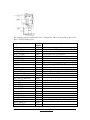
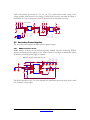
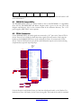
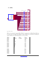
1
LOGIC Emulation Source
DN8000K10PCI
User Guide
1
LOGIC EMULATION SOURCE
DN8000K10PCI User Manual Revision 3
February 2, 2009 6:05 PM
© The Dini Group, 2005
7469 Draper Ave.
La Jolla, CA92037
Phone 858.454.3419 • Fax 858.454.1728
[email protected]
www.dinigroup.com
Table of Contents
ABOUT THIS MANUAL
1
.......................................................... 8
MANUAL CONTENTS .................................................................................................................................................... 9
ABOUT THIS MANUAL ................................................................................................................................................................. 9
QUICK START GUIDE ................................................................................................................................................................... 9
BOARD HARDWARE ..................................................................................................................................................................... 9
CONTROLLER SOFTWARE ............................................................................................................................................................ 9
REFERENCE DESIGN..................................................................................................................................................................... 9
FPGA DESIGN GUIDE ........................................................................................................ ERROR! BOOKMARK NOT DEFINED.
ORDERING INFORMATION ............................................................................................................................................................ 9
2
ADDITIONAL RESOURCES ......................................................................................................................................... 9
3
CONVENTIONS ............................................................................................................................................................. 10
3.1
TYPOGRAPHICAL ........................................................................................................................................................... 10
3.2
CONTENT ....................................................................................................................................................................... 11
3.2.1
File names ............................................................................................................................................................. 11
3.2.2
Physical orientation and Origin ........................................................................................................................... 11
3.2.3
Part Pin Names ..................................................................................................................................................... 12
3.2.4
Schematic Clippings .............................................................................................................................................. 12
3.2.5
Terminology .......................................................................................................................................................... 12
QUICK START GUIDE
............................................................. 14
1
PROVIDED MATERIALS ............................................................................................................................................ 14
2
ESD WARNING .............................................................................................................................................................. 15
3
POWER-ON INSTRUCTIONS ..................................................................................................................................... 15
3.1
VERIFY JUMPER SETTING .............................................................................................................................................. 17
3.2
VERIFY SWITCH SETTINGS ............................................................................................................................................ 17
3.3
MEMORY AND HEATSINKS ............................................................................................................................................. 19
3.4
PREPARE CONFIGRATION FILES ..................................................................................................................................... 19
3.5
CONNECT CABLES .......................................................................................................................................................... 20
3.6
VIEW CONFIGURATION FEEDBACK OVER RS232 .......................................................................................................... 21
3.6.1
Watch the configuration status output .................................................................................................................. 21
3.6.2
Interactive configuration ...................................................................................................................................... 24
3.6.3
Read temperature sensors ..................................................................................................................................... 24
3.6.4
Multiplex Serial port ............................................................................................................................................. 25
3.7
CHECK LED STATUS LIGHTS ......................................................................................................................................... 25
4
USING THE REFERENCE DESIGN WITH THE PROVIDED SOFTWARE ...................................................... 30
4.1
OPERATING THE USB CONTROLLER PROGRAM ............................................................................................................ 30
4.2
COMMUNICATING TO THE USER DESIGN OVER THE SERIAL PORT ............................................................................... 32
4.3
USING AETEST TO RUN HARDWARE TESTS ................................................................................................................. 33
4.3.1
AETest, Windows98 version.................................................................................................................................. 33
4.3.2
AETest, DOS version............................................................................................................................................. 33
4.3.3
AETest on Linux or Solaris ................................................................................................................................... 33
4.3.4
Use AETest ............................................................................................................................................................ 34
4.4
MOVING ON ................................................................................................................................................................... 35
CONTROLLER SOFTWARE
1
........................... 36
USB CONTROLLER...................................................................................................................................................... 36
1.1
MENU OPTIONS.............................................................................................................................................................. 36
1.1.1
File Menu .............................................................................................................................................................. 36
1.1.2
Edit Menu .............................................................................................................................................................. 37
1.1.3
FPGA Configuration Menu................................................................................................................................... 37
1.1.4
Settings/Info Menu ................................................................................................................................................ 38
2
PCI AETEST APPLICATION ...................................................................................................................................... 41
2.1
FUNCTIONALITY ............................................................................................................................................................ 41
2.2
RUNNING AETEST........................................................................................................................................................ 42
2.3
COMPILING AETEST .................................................................................................................................................... 42
2.3.1
Compiling AETest for DOS ................................................................................................................................... 42
2.3.2
Compiling AETest for Windows XP ...................................................................................................................... 43
3
UPDATING THE FIRMWARE .................................................................................................................................... 43
3.1
3.2
UPDATING THE MCU (FLASH) FIRMWARE .................................................................................................................... 43
UPDATING THE SPARTAN (EEPROM) FIRMWARE ........................................................................................................ 45
HARDWARE
4
........................................................................................................................ 49
OVERVIEW .................................................................................................................................................................... 49
5
CONFIGURATION CIRCUIT ..................................................................... ERROR! BOOKMARK NOT DEFINED.
5.1
OVERVIEW ..................................................................................................................................................................... 50
5.2
THE SPARTAN 2 FPGA .................................................................................................................................................. 51
Spartan Configuration .......................................................................................................................................... 52
5.2.1
5.2.2
Smart Media .......................................................................................................................................................... 53
5.2.3
MCU communication ............................................................................................................................................ 54
5.2.4
PCI commnication................................................................................................................................................. 54
5.2.5
RS232 .................................................................................................................................................................... 54
5.2.6
IIC .......................................................................................................................................................................... 55
5.3
CONFIGURATION OPTIONS ............................................................................................................................................ 55
5.3.1
Jtag ........................................................................................................................................................................ 56
5.3.2
SmartMedia ........................................................................................................................................................... 57
5.3.3
USB........................................................................................................................................................................ 59
5.3.4
PCI ........................................................................................................................................................................ 60
5.4
FPGA CONFIGURATION PROCESS ................................................................................................................................. 62
5.5
MCU .............................................................................................................................................................................. 63
5.5.1
RS232 .................................................................................................................................................................... 64
5.5.2
Clocks .................................................................................................................................................................... 64
5.5.3
LEDs ...................................................................................................................................................................... 65
5.5.4
Memory space ....................................................................................................................................................... 65
5.5.5
USB........................................................................................................................................................................ 68
5.5.6
Smart media .......................................................................................................................................................... 69
U
6
CLOCKING ..................................................................................................................................................................... 70
6.1
6.2
6.3
7
8
GLOBAL CLOCKS ........................................................................................................................................................... 73
USER CLOCK .................................................................................................................................................................. 77
FEEDBACK CLOCKS ....................................................................................................................................................... 78
RESET TOPOLOGY...................................................................................................................................................... 78
POWER ............................................................................................................................................................................ 80
8.1
SWITCHING POWER SUPPLIES ........................................................................................................................................ 82
8.2
SECONDARY POWER SUPPLIES ...................................................................................................................................... 83
8.2.1
DDR2 Termination Power .................................................................................................................................... 83
8.2.2
RocketIO power ..................................................................................................................................................... 84
8.2.3
Optical Module Power .......................................................................................................................................... 84
8.3
HEAT DISSIPATION ......................................................................................................................................................... 85
9
FPGA INTERCONNECT .............................................................................................................................................. 86
9.1
10
MAIN BUS ...................................................................................................................................................................... 89
MEMORY INTERFACE ............................................................................................................................................... 89
10.1
10.2
11
CLOCKING.................................................................................................................................................................. 90
SERIAL PRESENCE DETECT. ....................................................................................................................................... 90
HEADERS........................................................................................................................................................................ 91
11.1
11.2
11.3
11.4
11.5
11.6
3000K10 COMPATIBILITY ......................................................................................................................................... 93
FPGA CONNECTION .................................................................................................................................................. 93
IO POWER .................................................................................................................................................................. 98
PHYSICAL................................................................................................................................................................... 99
DAUGHTERCARD POWER........................................................................................................................................... 99
THE MICTOR ............................................................................................................................................................ 100
12
LEDS............................................................................................................................................................................... 102
13
ROCKETIO ................................................................................................................................................................... 103
13.1
13.2
13.2.1
13.3
13.4
13.5
13.5.1
13.5.2
13.6
14
14.1
14.2
14.3
14.4
14.5
14.6
14.7
14.8
ROCKETIO CLOCK RESOURCES .............................................................................................................................. 103
MGT POWER NETWORK .......................................................................................................................................... 106
FX CES2 rework ............................................................................................................................................. 106
THE CONNECTIONS .................................................................................................................................................. 107
SAMTEC MULTI GIGABIT RIBBON CABLE ................................................................................................................ 110
OPTICAL MODULES ................................................................................................................................................. 112
SFP .................................................................................................................................................................. 112
XFP.................................................................................................................................................................. 113
THE SMAS ............................................................................................................................................................... 115
PCI INTERFACE ......................................................................................................................................................... 115
PCI EDGE CONNECTOR ............................................................................................................................................ 115
THE QUICKLOGIC 5064 ........................................................................................................................................... 116
VIRTEX 4 FPGA COMMUNICATION ........................................................................................................................ 116
SPARTAN 2 COMMUNICATION ................................................................................................................................. 116
PCI CLOCKING ......................................................................................................................................................... 118
JTAG ....................................................................................................................................................................... 118
PCI POWER .............................................................................................................................................................. 118
PCI SIGNALING ........................................................................................................................................................ 119
15
FPGA SYSTEM MONITOR/ADC ............................................................................................................................. 120
16
MECHANICAL ............................................................................................... ERROR! BOOKMARK NOT DEFINED.
1
EXPLORING THE REFERENCE DESIGN ............................................................................................................. 122
1.1
2
WHAT IS THE REFERENCE DESIGN? ............................................................................................................................ 122
REFERENCE DESIGN MEMORY MAP ................................................................................................................. 123
2.1
USING THE REFERENCE DESIGN .................................................................................................................................. 126
2.1.1
Built-In RocketIO test.......................................................................................................................................... 127
3
MEMORY MAPPED DATA FLOW ............................................................ ERROR! BOOKMARK NOT DEFINED.
3.1
COMPILING THE REFERENCE DESIGN .......................................................................................................................... 133
3.1.1
The Xilinx Embedded Development Kit (EDK) .................................................................................................. 133
3.1.2
Xinlinx XST..............................................................................................................Error! Bookmark not defined.
3.1.3
Xilinx ISE............................................................................................................................................................. 134
3.1.4
The Build Utility: Make.bat ................................................................................................................................ 134
4
GETTING MORE INFORMATION.......................................................................................................................... 134
4.1
PRINTED DOCUMENTATION ......................................................................................................................................... 138
4.2
4.3
5
FPGA OPTIONS ........................................................................................................................................................... 141
5.1
5.2
5.3
6
FPGA A: ...................................................................................................................................................................... 141
FPGA B: ...................................................................................................................................................................... 141
FPGA C: ...................................................................................................................................................................... 142
MULTI-GIGABIT SERIAL OPTIONS ..................................................................................................................... 142
6.1
6.2
7
SERIAL CLOCK CRSTALS ............................................................................................................................................. 142
MODULE SOCKETS....................................................................................................................................................... 142
OTHER OPTIONS ....................................................................................................................................................... 143
7.1
7.2
8
ELECTRONIC DOCUMENTATION .................................................................................................................................. 138
ONLINE DOCUMENTATION .......................................................................................................................................... 138
3.3 V HEADERS ............................................................................................................................................................ 143
12V POWER ................................................................................................................................................................. 143
OPTIONAL EQUIPMENT .......................................................................................................................................... 143
1
Chapter
About This Manual
:
r1
te
p
a
h
C
Welcome to DN8000K10PCI Logic Emulation Board
Congratulations on your purchase of the DN8000K10PCI LOGIC Emulation
Board. If you are unfamiliar with Dini Group products, you should read Chapter 2,
Quick Start Guide to familiarize yourself with the user interfaces the DN8000K10PCI
provides.
Figure 1 DN8000K10PCI
1 Manual Contents
This manual contains the following chapters:
About This Manual
List of available documentation and resources available. Reader’s Guide to this manual
Quick Start Guide
Step-by-step instructions for powering on the DN8000K10PCI, loading and communicating
with a simple provided FPGA design and using the board controls.
Board Hardware
Detailed description and operating instructions of each individual circuit on the
DN8000K10PCI
Controller Software
A summary of the functionality of the provided software. Implementation details for the remote
USB board control functions and instructions for developing your own USB host software.
Reference Design
Detailed description of the provided DN8000K10PCI reference design. Implementation details
of the reference design interaction with DN8000K10PCI hardware features.
Ordering Information
Contains a list of the available options and available optional equipment. Some suggested parts
and equipment available from third party vendors.
2 Additional Resources
For additional information, go to http://www.dinigroup.com. The following table lists some of
the resources you can access from this website. You can also directly access these resources
using the provided URLs.
Resource
Descripti
on/URL
UserDN8000K10PCI
User Guide
This is the main source of technical information. The manual
should contain most of the answers to your questions
Dini Group Web Site
The web page will contain the latest manual, application
notes, FAQ, articles, and any device errata and manual
addenda. Please visit and bookmark:
http://www.dinigroup.com
DN8000K10PCI User Guide
www.dinigroup.com
9
Resource
Virtex 4 User Guide
Descripti
on/URL
Xilinx publication UG070
http://www.xilinx.com/bvdocs/userguides/ug070.pdf
Most of your questions regarding usage and capabilities of
the Virtex 4 devices will be answered here, including
readback, boundary scan, configuration, and debugging
E-Mail
You may direct questions and feedback to the Dini Group
using this e-mail address: [email protected]
Phone Support
Call us at 858.454.3419 during the hours of 8:00am to 5:00pm
Pacific Time.
FAQ
The download section of the web page contains a document
called DN8000K10PCI Frequently Asked Questions
(FAQ). This document is periodically updated with
information that may not be in the User’s Manual.
Figure 2 Support Resources
3 Conventions
This document uses the following conventions. An example illustrates each convention.
3.1 Typographical
The following typographical conventions are used in this document:
Convention
Meaning or Use
Example
Courier font
Messages, prompts, and
program files that the system
displays
speed grade: 100
Courier bold
Literal commands that you
enter in a syntactical statement
ngdbuild
design_name
Commands that you select
from a menu
File ÆOpen
Keyboard shortcuts
Ctrl+C
Variables in a syntax statement
for which you must supply
values
ngdbuild design_name
Garamond bold
DN8000K10PCI User Guide
www.dinigroup.com
10
Convention
Meaning or Use
Example
References to other manuals
See the Development System
Reference Guide for more
information.
Italic font
Emphasis in text
If a wire is drawn so that it
overlaps the pin of a
symbol, the two nets are
not connected.
Braces [ ]
An optional entry or
parameter. However, in bus
specifications, such as bus[7:0],
they are required.
ngdbuild [option_name]
design_name
Braces { }
A list of items from which you
must choose one or more
lowpwr ={on|off}
Vertical bar |
Separates items in a list of
choices
lowpwr ={on|off}
Vertical ellipsis
Repetitive material that has
been omitted
IOB #1: Name = QOUT’
-
IOB #2: Name = CLKIN’
-
-
-
-
Horizontal ellipsis . . .
Repetitive material that has
been omitted
allow block block_name
Prefix “0x” or suffix
“h”
Indicates hexadecimal notation
Read from address
0x00110373, returned
4552494h
Letter “#” or “_n”
Signal is active low
INT# is active low
loc1 loc2 ... locn;
fpga_inta_n is active low
3.2 Content
3.2.1
File names
Paths to documents included on the User CD are prefixed with “D:\”. This refers to your CD
drive’s root directory, or the directory where you have copied the CD contents.
3.2.2
Physical orientation and Origin
By convention, the board is oriented as show on page 3, with the “top” of the board being the
edge near Headers A and B, and the edge with the optical module connectors. The “right” edge
is near the SMA connectors, the “left” side is the side with the PCI bezel. “topside” refers to the
DN8000K10PCI User Guide
www.dinigroup.com
11
side of the PWB with FPGAs soldered to it, “backside” is the side with the daughter card
connectors. The reference origin of the board is the center of the lower PCI bezel mounting
hole.
3.2.3
Part Pin Names
Pin names are given in the form <X><Y>.<Z>; The <X> is one of: U for ICs, R for resistors,
C for capacitors, P or J for connectors, FB or L for inductors, TP for test points, MH for
mounting structures, FD for fiducials, BT for sockets, DS for diodes, F for fuses, HS for
mechanicals, PSU for power supply modules, Q for discreet semiconductors, RN for resistor
networks, X for oscillators, Y for crystals. <Y> is a number uniquely identifying each part from
other parts of the same X class on the same PWB. <Z> is the pin or terminal number or name,
as defined in the datasheet of the part. Datasheets for all standard and optional parts used on the
DN8000K10PCI are included in the Document library on the provided User CD.
3.2.4
Schematic Clippings
3.2.5
Terminology
Partial schematic drawings are included in this document to aid quick understanding of the
features of the DN8000K10PCI. These clippings have been modified for clarity and brevity, and
may be missing signals, parts, net names and connections. Unmodified Schematics are included
in the User CD. Please refer to this document. Use the PDF search feature to search for nets
and parts.
D:\Schematics\REV3\Schematic_DN8000K10PCI_503-0121-0000_rev03.pdf
Abbreviations and pronouns are used for some commonly used phrases.
MGT and RocketIO are used interchangeably. MGT is multi-gigabit transceiver. RocketIO is
the Xilinx trademark on their multi gigabit transceiver hardware.
MCU is the Cypress FX2 Microcontroller, U39
DN8000K10PCI User Guide
www.dinigroup.com
12
2
Chapter
Quick Start Guide
:
r2
te
p
a
h
C
The Dini Group DN8000K10PCI is the user-friendliest board
available with multiple Virtex 4 FPGAs. However, due to the number
of features and flexibility of the board, it will take some time to become
familiar with all the control and monitoring interfaces equipped on the
DN8000K10PCI. Please follow this quick start guide to become
familiar with the board before starting your ASIC emulation project.
1 Provided Materials
Examine the contents of your DN8000K10PCI kit. It should contain:
•
DN8000K10PCI board
•
Two Smart Media cards
•
USB SmartMedia card reader
•
RS232 IDC header cable to female DB9
•
USB cable
•
CD ROM containing:
- Virtex 4 Reference Design
- Virtex 4 Documentation (Datasheets)
- User manual PDF
- Board Schematic PDF
- Board netlist TXT
- USB Windows program (usbcontroller.exe)
- USB Windows documentation
- PCI program (Aetestdj.exe)
- Source code for USB program, PCI program and DN8000K10PCI firmware
You should use the customer netlist provided on the user CD for the purpose of generating
designs and should consult the schematic PDF provided on the CD when designing any
hardware to interface to the DN8000K10PCI. All other documentation materials are derived
from this schematic.
For information about the USB Controller program, see the document accompanying the
program on the CD.
2 ESD Warning
The DN8000K10PCI is sensitive to static electricity, so treat the PCB accordingly. The target
markets for this product are engineers that are familiar with FPGAs and circuit boards.
However, if needed, the following web page has an excellent tutorial on the “Fundamentals of
ESD” for those of you who are new to ESD sensitive products:
http://www.esda.org/basics/part1.cfm
There are two large grounded metal rails on the DN8000K10PCI.
The DN8000K10PCI has been factory tested and pre-programmed to ensure correct operation.
reference design is included on the provided CD and SmartMedia card.
The 200-pin connectors are not 5V tolerant. According to the Virtex 4 datasheets, the
maximum applied voltage to these signals is VCCO + 0.5V (3.0V while powered on). These
connections are not buffered, and the Virtex 4 part is sensitive to ESD. Take care when
handling the board to avoid touching the daughter card connectors.
3 Power-On Instructions
The image below represents your DN8000K10PCI. You will need to know the location of the
following parts referenced in this chapter.
RS232 P2
DN8000K10PCI User Guide
www.dinigroup.com
15
ATX Power
SW1-SW4
USB port
SmartMedia
JP1
DDR2 SODIMM
A
Figure 3 DN8000K10PCI configuration controls
To begin working with the DN8000K10PCI, follow the steps below :
DN8000K10PCI User Guide
www.dinigroup.com
16
3.1 Verify Jumper Setting
The DN8000K10PCI uses a jumper to configure the PCI interface IO signal levels. Please
locate the jumper block on your board and verify that it matches the default settings. By default,
this jumper is installed from JP1.2-JP1.4
Table 1 – describes the functionality of the jumper block on the DN8000K10PCI.
Table 1 – Jumper Description
Jumper Location
Signal Name
Description
JP1.1 – JP1.3
BOARD 5V
This jumper fixes the PCI clamping
voltage at 5.0V. You should use this
jumper setting if the DN8000K10PCI is
being used in stand-alone mode
JP1.2 – JP1.4 (default)
PCI VIO
This jumper should be installed when the
board is being operated in a 5V or 3.3V
PCI slot.
Don’t install both jumpers at the same
time.
The "top" two pins are 1 and 3. Pin 1 is the one with a white circle next to it. There is a label
next to each pin indicating it's connection:
1 - BOARD 5V
2 - BOARD VIO
3 - BOARD VIO
4 - PCI VIO
BOARD 5V - BOARD VIO (1-3) is correct when the board is not in PCI.
PCI VIO - BOARD VIO (2-4) is correct when in a PCI slot.
The effect of an incorrect setting when in PCI is less reliability in a very heavily loaded PCI slot
at 66 Mhz. The effect of the incorrect setting when not in a PCI slot is the temperature sensors
might not work.
3.2 Verify Switch Settings
The DN8000K10PCI uses a DIP switch to program the FPGA configuration circuitry. The
function of these DIP switches is Listed in Table 2. Verify that the switch settings on your board
match the default settings.
Table 2 – Switch Description
DN8000K10PCI User Guide
www.dinigroup.com
17
Switch
Default
Position
Signal Name
S1-1
Off
Reserved
S1-2
Off
Reserved
S1-3
Off
Boot mode
S1-4
Off
Reserved
DN8000K10PCI User Guide
On setting
Off setting
Firmware update
Normal operation (default)
www.dinigroup.com
18
3.3 Memory and heatsinks
There should be an active heatsink installed on each FPGA on the DN8000K10PCI and a fan
over the power supply units. Virtex 4 FPGAs are capable of dissipating 15W or more, so you
should always run them with heatsinks installed.
The DN8000K10PCI comes packaged without memory installed. If you want the Dini Group
reference design to test your memory modules, you can install them now in the 1.8V DDR2
DIMM sockets.
FPGA C
FPGA B
FPGA A
DIMM B
DIMM C
Figure 4 FPGA Names
The socket DIMMB is connected to FPGA B. The socket can accept any capacity DDR2
SODIMM module. Note that DDR1 modules will not work in these slots since they are
supplied with 1.8V power and DDR1 requires 2.5V power (and a completely different pin-out).
3.4 Prepare configuration files
The DN8000K10PCI reads FPGA configuration data from a SmartMedia card. To program the
FPGAs on the DN8000K10PCI, FPGA design files (with a .bit file extension) put on the root
directory of the SmartMedia card file using the provided USB card reader.
The DN8000K10PCI ships with a 32 MB SmartMedia card preloaded with the Dini Group
reference design.
DN8000K10PCI User Guide
www.dinigroup.com
19
1. Insert the provided SmartMedia card labeled “Reference Design” into your USB card
reader. Make sure the card contains the files:
FPGA_A.bit
FPGA_B.bit
FPGA_C.bit
main.txt
The files FPG_A-C.bit are files created by the Xilinx program bitgen, part of the ISE
7.1 tools. The file main.txt contains instructions for the DN8000K10PCI configuration
circuitry, including which FPGAs to configure, and to which frequency the global clock
networks should be automatically adjusted.
2. Insert the SmartMedia card labeled “Reference Design” into the DN8000K10PCI’s
SmartMedia slot, contacts down.
3.5 Connect cables
The configuration circuitry can accept user input to control FPGA configuration or provide
feedback during the configuration process. The configuration circuitry IO can also be used to
transfer data to and from the user design.
1. Use the provided ribbon cable to connect the MCU RS232 port (P2) to a computer
serial port to view feedback from the configuration circuitry during FPGA
configuration. Run a serial terminal program on your PC (On Windows you can use
HyperTerminal
Start->Programs->Accessories->Communications->HyperTerminal) and make sure
the computer serial port is configured with the following options:
•
Bits per second: 19200
•
Data bits: 8
•
Parity: None
•
Stop Bits: 1
•
Flow control: None
•
Terminal Emulation: VT100
2. Use the provided USB cable to connect the DN8000K10PCI to a Windows computer
(Windows XP is recommended).
DN8000K10PCI User Guide
www.dinigroup.com
20
3. Plug an ATX power supply into J1, or plug the DN8000K10PCI into a PCI slot. Do
not plug an external power supply into J1 if the DN8000K10PCI is plugged into a
PCI slot. Turn on the ATX power supply.
When the DN8000K10PCI powers on, it automatically loads Xilinx FPGA design files (ending
with a .bit extension), found on the SmartMedia card in the SmartMedia slot into the FPGAs.
3.6 View configuration feedback over RS232
As the DN8000K10PCI powers on, your RS232 terminal (connected to P2) will display useful
information about the Configuration process.
3.6.1
Watch the configuration status output
DN8000K10PCI User Guide
www.dinigroup.com
21
No USB cable detected, rebooting from FLASH...please wait
Setting ACLK…
N 01 M: 000001000
DONE
Setting BCLK...
N: 01 M: 000001000
DONE
Setting DCLK...
N: 01 M: 000001000
DONE
Setting R1CLK...
N: 01 M: 000001000
DONE
Setting R2CLK...
N: 01 M: 000001000
DONE
=-=- DN8000k10PCI MCU FLASH BOOT -=-=
-- FPGAS STUFFED -AB
-- SMART MEDIA INFO -MAKER ID: EC
DEVICE ID: 75
SIZE: 32 MB
-- FILES FOUND ON SMART MEDIA CARD
FPGA_B.BIT
FPGA_A.BIT
MAIN~1.TXT
MAIN.TXT
-- CONFIGURATION FILES -FPGA A: FPGA_A.BIT
FPGA B: FPGA_B.BIT
--OPTIONS-Message level set to default: 2
Sanity check is set to default: ON
N: 00 M: 000001010
DONE
Setting BCLK...
N: 01 M: 000001100
DONE
Setting DCLK...
N: 01 M: 000001000
DONE
Setting R1CLK...
N: 01 M: 000001000
DONE
Setting R2CLK...
N: 01 M: 000001000
DONE
****************************CONFIGURING FPGA:
A****************************
-- Performing Sanity Check on Bit File --- BIT FILE ATTRIBUTES -FILE NAME: FPGA_A.BIT
FILE SIZE: 003A943B bytes
PART: 4vlx100ff151317:09:38
DATA: 2005/07/25
TIME: 17:09:38
The global clocks (ACLK, BCLK, DCLK) are frequencyconfigurable. The M binary sequence represents the multiplication
applied to the installed crystal. The N represents the division applied.
U6, U14, U20, U31 and the ICS8442AY datasheet.
The MCU is setting the clocks to their default values ACLK 200Mhz,
BCLK 108.8Mhz, DCLK 128Mhz, R1CLK (not available on
DN8000K10PCI), R2CLK (**DEFAULT**)
The MCU detects which FPGAs are present
The MCU detects if a SmartMedia card is present
The MCU tries to access the SmartMedia card. If the MCU is not
successful in reading the files on the SmartMedia card, be sure you
have not formatted the card in Windows. Windows uses a nonstandard format for media cards and will make the card unreadable.
You can download a format utility from dinigroup.com to repair your
incorrectly-formatted SM card.
The MCU reads the contents of the file MAIN.TXT and executes
each instruction line.
Here the MCU is setting the clocks according to instructions in
MAIN.TXT
The MCU is configuring FPGA A according to instructions in
MAIN.TXT
The sanity check option reads the design (“.bit”) file headers and
verifies that the design is compiled for the same type of FPGA that
the MCU detects on your DN8000K10PCI. If the design and FPGA
do not match, the MCU will reject the file and flash the Error LED.
You may need to disable to sanity check option (See Chapter X,
section X) if you want to encrypt or compress your configuration
Sanity check passed
................................................................................................................
................................................................................................................
..........DONE WITH CONFIGURATION OF FPGA: A
files.
****************************CONFIGURING FPGA
B****************************
-- Performing Sanity Check on Bit File --- BIT FILE ATTRIBUTES -FILE NAME: FPGA_B.BIT
FILE SIZE: 003A943B bytes
PART: 4vlx100ff151317:05:01
DATA: 2005/07/19
TIME: 17:05:01
Sanity check passed
................................................................................................................
................................................................................................................
..........DONE WITH CONFIGURATION OF FPGA: B
The MCU is configuring FPGA B according to instructions in
MAIN.TXT
The MCU is setting the temperature threshold to cause a board reset.
-- TEMPERATURE SENSORS -A YES
B YES
FPGA Temperature Alarm Threshold: 80 degrees C
DN8000k10PCI MAIN MENU (Jul 27 2005 10:38:05)
1.) Configure FPGAs using "MAIN TXT"
2.) Interactive configuration menu
3.) Check configuration status
4.) Change MAIN configuration file
5.) List files on Smart Media
6.) Display Smart Media text file
7.) Change RS232 PPC Port
8.) Set FPGA Address
9.) Write to FPGA at current address
a.) Read from FPGA at current address
g.) Display FPGA Temperatures
h.) Set FPGA Temperature Alarm Threshold
ENTER SELECTION:
Here is the MCU main menu
Options 8,9, and A are only available when the DN8000K10PCI
reference design is loaded. For more information on how the MCU
communicates with the reference design, see Chapter X, The
Reference Design.
Figure 5 RS232 Output
You should see the DN8000K10PCI MCU main menu. If the reference design is loaded in the
Virtex 4 FPGAs, then you should see the above on your terminal. Try pressing 3 to see if the
configuration circuit was successful in programming the FPGAs.
ENTER SELECTION: 3
********************* CONFIGURATION STATUS *******************
FPGA B NOT configured
The easiest way to verify your FPGAs are configured is to look at DS18, DS14, DS16 located
above each FPGA. When the green LEDs are lit, the FPGA under it is successfully configured.
DN8000K10PCI User Guide
www.dinigroup.com
23
3.6.2
Interactive configuration
If you want to put multiple designs on a single Smart Media card, you can use the interactive
configuration menu to select which .bit file to use on each FPGAs. Select menu option 2.
ENTER SELECTION: 2
-=-= INTERACTIVE CONFIGURATION MENU =-=-
1) Select bit files to configure FPGA(s)
2) Set verbose level (current level = /)
3) Enable sanity check for bit files
M) Main Menu
Enter Selection:
Figure 6 Interactive Config Menu
3.6.3
Read temperature sensors
The DN8000K10PCI is equipped with temperature sensors to measure and monitor the
temperature on the die of the Virtex 4 FPGAs. According to the Virtex 4 datasheet, the
maximum recommended operating temperature of the die is 85C degrees. If the microcontroller
measures a temperature above 80 degrees, it will reset the DN8000K10PCI.
If you think your DN8000K10PCI is resetting due to temperature overload, you can use the
temperature monitor menu to measure the current junction temperature of each FPGA.
ENTER SELECTION: g
-- FPGA TEMPERATURES (Degrees Celsius [+/- 4]) -B 29
-- Set FPGA Temperature Alarm Threshold
--
(degrees C, decimal values, range [1-127])
Old Threshold: 80
New Threshold: 85
Threshold Updated: 85 Degrees C
Figure 7 Temperature Threshold Menu
The Virtex 4 FPGA can operate as hot as 120C degrees before damaging the part, although
timing specifications are not guaranteed. The MCU allows you to change the reset threshold,
DN8000K10PCI User Guide
www.dinigroup.com
24
although we recommend improving your heat dissipation to maintain a low junction
temperature.
3.6.4
Multiplex Serial port
The DN8000K10PCI has one serial port (P1) for user use. This single port is multiplexed so
that any FPGA can access it through its RX and TX signals. You can use the RS232 MCU
interface to change the FPGA to which P1 is connected.
ENTER SELECTION: 7
PORT 1: D
PORT 2: A
PORT 3: A
PORT 4: A
Enter Port to change (1-4, q to quit): 1
Enter FPGA to set port to (A-I): B
Do you want to change more RS232 Ports (y or n)?: n
Figure 8 RS232 Port Menu
The DN8000K10PCI only has one serial port (Port 1). Changing ports 2-4 will have no effect.
3.7 Check LED status lights
The DN8000K10PCI has many status LEDs to help the user confirm the status of the
configuration process.
DN8000K10PCI User Guide
www.dinigroup.com
25
Power
supply status
FPGA A User LEDs
(bottom)
FPGA A status
Configuration
Activity
Configuration
Control status
Spartan 2
LEDs
FPGA B
status
MCU LEDs
Spartan FPGA
status
Figure 9 Configuration Status LEDs
1.
Check the power voltage indication LEDs to confirm that all voltage rails of the
DN8000K10PCI are present. From the top, the LEDs indicate the presence of
5V, 3.3V, 2.5V, and “ATX POWER OK” Green lit LED’s on the voltage
present LEDs indicate the rails are greater than 1.7V. A green lit “ATX power
OK” indicates that the voltage monitors inside the ATX power supply are
within acceptable operating ranges (5V is 4.5 – 5.5V, 3.3V is 3.0-3.6V). If this
LED is not lit green, the DN8000K10PCI might not function properly.
2.
Check the Configuration status LEDs. These LEDs are visible from outside the
case when the DN8000K10PCI is installed in an ATX case. Under error
conditions, all four red LEDs will blink.
3.
Check the Spartan FPGA status LED, DS24. This LED indicates that the
Spartan II FPGA has been configured. If this LED is not lit soon after power
on, then there may be a problem with the firmware on the DN8000K10PCI.
This LED off or blinking may indicate a problem with one of the board’s
power supplies.
DN8000K10PCI User Guide
www.dinigroup.com
26
4.
Check the FPGA A status LED, DS18 to the upper left of FPGA A. This
green LED is lit when FPGA A is configured and operational. This light should
be on if you loaded the reference design from the SmartMedia card.
5.
Check the FPGA B status LED, DS14 directly above FPGA B. This light
should be lit green if your DN8000K10PCI was installed with the FPGA B
option, and the reference design is loaded.
6.
Check the FPGA C status LED, DS16 to the upper left of FPGA C. This green
LED will light if you have the FPGA C option and the FPGA is configured.
7.
Check the FPGA A User LEDs on the bottom side of the DN8000K10PCI. If
you have successfully loaded the Dini Group’s DN8000K10PCI reference
design, these should be lit in the pattern “00011010”.
8.
Check the FPGA C User LEDs on the bottom side of the DN8000K10PCI. If
you have ordered the “FX” FPGA C option, and the reference design is loaded,
these be lit in the pattern “1110110111001011”.
9.
If you suspect one or more FPGAs did not configure properly, check the
configuration circuitry’s status lights. These are four right-angle mounted LEDs
viewable out the side of the PC case. If there has been an error, three of the
LEDs will blink. If there has been no error, there should be two LEDs ON and
two OFF. If there was an error, the easiest way to determine the cause of the
error is to connect a terminal to the RS232 port (P2) and try to configure again.
Configuration feedback will be presented over this port.
You should also notice the Fans mounted above the 3 Virtex 4 FPGAs and the Fan mounted
above the power supplies spinning.
Assembly Number
Signal
Comment
DS9
5.0V_PRESENT
The 5.0V power rail is
present (above ~1.7V)
DS10
3.3V_PRESENT
The 3.3V power rail is
present (above ~1.7V)
DS11
2.5V_PRESENT
The 2.5V power rail is
present (above ~1.7V)
DS12
1.8V_PRESENT
The 1.8V power rail is
present (above ~1.7V)
DS13
ATX_POK
The ATX power supply is
generating 5.0V and 3.3V
DN8000K10PCI User Guide
www.dinigroup.com
27
within 5% at the source
DS15
SPARTAN_LED3
This LED will flicker when
there is PCI configuration
activity (Bar 0)
DS17
SPARTAN_LED2
This LED will flicker when
there is Main Bus activity
(See section X.X.X)
DS19
SPARTAN_LED1
This LED will flicker when
there is USB activity (Bulk
Transfer)
DS20
SPARTAN_LED0
This LED will flicker when
there is SmartMedia card
activity.
DS21.1
MCU_LED0
MCU_LED[1:0] Codes:
DS21.2
MCU_LED1
01 FPGA A is configuring
10 FPGA B is configuring
11 FPGA C is configuring
DS21.3
MCU_LED2
The
last
configuration
successful
DS21.4
MCU_LED3
Blinking: There was a
configuration error. Use
the RS232 port to read the
error. Off: No error. On:
The last configuration
command was successful
DS24
SPARTAN_DONE
The
Spartan
2
configuration FPGA is
configured. This light will
turn off if the board is in
power reset
DN8000K10PCI User Guide
www.dinigroup.com
FPGA
was
28
DS22
PCI_IN
PCI data is arriving from
the PCI bus
DS23
PCI_OUT
PCI data is being
transmitted onto the PCI
bus
DS18
FPGA_A_DONE
The Virtex 4 FPGA A is
configured
DS14
FPGA_B_DONE
The Virtex 4 FPGA B is
configured
DS16
FPGA_C_DONE
The Virtex 4 FPGA C is
configured
DS8
SFP2_LOS
SFP module 2 Loss-ofsignal
DS4
SFP2_FAULT
SFP module 2 transmitter
fault
DS5
XFP2_INT
XFP module 2 error
DS1
XFP2_FAULT
XFP module 2 transmitter
fault
DS6
SFP1_LOS
SFP module 1 Loss-ofsignal
DS2
SFP1_FAULT
SFP module 1 transmitter
fault
DS7
XFP1_INT
XFP module 1 error
DS3
XFP1_LOS
XFP module 1 Loss-ofsignal
DS48, DS47, DS46, DS45,
DS44, DS43, DS42,
DS41,
DN8000K10PCI User Guide
User LEDs from FPGA C
www.dinigroup.com
29
DS40,DS39, DS38, DS37,
DS36, DS35, DS34, DS33,
User LEDs from FPGA C
DS32, DS31, DS30, DS29,
DS28, DS27, DS26, DS25
User LEDs from FPGA A
Figure 10 DN8000K10PCI LEDs
4 Using the Reference Design with the Provided
Software
To communicate with the reference design (or user design) on the emulation board, the
DN8000K10PCI provides three options out of the box.
•
USB
•
PCI
•
RS232
The USB and PCI interfaces allow configuration of the FPGAs and bulk data transfer to and
from the User design. The RS232 interface allows low-speed data transfers to and from the User
design, and control and monitoring of the configuration process.
This section will get you started and show you how to operate the provided software. For
detailed information about the reference design and implementation details, see Chapter 5, The
Reference Design.
4.1 Operating the USB controller program
Use the provided USB monitoring software to verify that the design is loaded into the FPGAs.
1. Insert the CDROM that came with your DN8000K10PCI into the CDROM drive of
your computer.
2. Connect the USB cable to your DN8000K10PCI and a Windows XP PC. (Before or
after the DN8000K10PCI has powered on)
3. When you connect the USB cable to your PC for the first time, Windows detects the
DN8000K10PCI and asks for a driver. The board should identify itself as a “DiNi Prod
FLASH BOOT”. When the new device detected window appears, select the option
"install from a list" -> select "search for the best driver in these locations". Select
"include the location in the search" and browse to the product CD in
“Source Code\AETEST_USB\driver\win_wdm\” ->select "finish"
DN8000K10PCI User Guide
www.dinigroup.com
30
4. After Windows installs the driver, you will be able to see the following device in the
USB section of Windows device manager: “DiniGroup DN8000K10PCI FLASH
boot”.
5. Run the USB controller application found on the product CD in “Source
Code\USBController\USBController.exe”.
Figure 11 USB Controller Window
6. This window will appear showing the current state of the DN8000K10PCI. Next to each
FPGA a green light will appear if that FPGA is configured successfully. The above
window shows the USB Controller connected to a DN8000K10PCI with a single FPGA
in the B position. If you have the reference design loaded and a DDR2 SODIMM
installed, you can use the USB Controller to run tests of the SODIMM. From the FPGA
Memory menu, select Test DDR.
7. Clear the FPGAs of their configurations. Right-click on an FPGA and select from the
popup menu, “Clear FPGA”. The green light above the FPGA on the GUI and on the
board should stop shinning green.
8. Configure an FPGA using the USB Controller program. Right-click on an FPGA and
select Configure FPGA via USB from the popup menu. The program will open a dialog
DN8000K10PCI User Guide
www.dinigroup.com
31
box for you to select the configuration file to use for configuration. Browse to the
provided user’s CD
D:\FPGA_Reference_Designs\Programming_Files\DN8000K10PCI\MainTest\LX100
If you are configuring an LX200 or FX60 devices you should select a bit file from the
LX200 or FX60 directories instead. If you are configuring FPGA B or FPGA C, you
should select fpga_b.bit or fpga_c.bit instead.
Done
FPGA B cleared successfully.
FPGA A cleared successfully.
Doing a sanity check...Sanity Check passed. Configuring FPGA
B via USB...please wait.
File
D:\\dn_BitFiles\DN8000K10PCI\MainTest\LX100\fpga_b.bit
transferred.
Configured FPGA B via USB
Figure 12 USB Controller Log Output
9. The message box below the DN8000K10PCI graphic should display some information
about the configuration process
The USB Controller program also allows you to easily configure and transfer data to and from
the user design on the emulation board. More information is provided in Chapter 3, “Controller
Software”
4.2 Communicating to the User Design over the Serial Port
You may want to communicate with your design over the user serial port (P1). Only one FPGA
can use P1 at a time. Before you can communicate to your design, change the RS232
multiplexing settings as described in Section 3.6.4. You can also change the RS232 multiplexing
settings using the USB Controller software.
Connect a second RS232 cable to P1, the FPGA RS232. It is located right next to the
configuration RS232 port, P2. If you have the reference design loaded, the FPGA RS232 port
runs at 19200 bps, 8 bit, no parity. By default, the FPGA RS232 port is connected to FPGA A.
One the computer’s terminal, the reference design is programmed to digitally loop back the
input to the output. If on the terminal you can read your own output, then the reference design
was able to capture the RS232 signal and generate an RS232 signal that your computer could
capture.
If you are familiar with previous Dini Group products, the reference design test outputs could
be read from this serial port. On the DN8000K10PCI, you must use the AETEST application
to read the results of self-test.
DN8000K10PCI User Guide
www.dinigroup.com
32
4.3 Using AETEST to run hardware tests
AETest is the program that you can use to verify the hardware on the DN8000K10PCI, as well
as to demonstrate the reference design function. The following instructions assume you have a
PC running the Windows XP operating system. The user CD includes a Windows version of
the AETest program. If you plan to use the DN8000K10PCI in stand-alone mode, connect the
DN8000K10PCI to your WindowsXP computer and use aetest_usb in
D:\USB_Software_Applications\USB_CMD_Line_AETEST_USB. If the computer asks for a
driver, click “Have Disk” and browse to
D:\USB_Software_Applications\driver\windows_wdm\dndevusb.inf
If you are going to use the DN8000K10PCI in a PCI slot, turn off the computer, insert the
DN8000K10PCI into an unused PCI slot, and turn the computer on. If the operating system
asks for a driver, click “Have Disk” and browse to
Then run the PCI version of the AETest application at
D:\USB_Software_Applications\USB_CMD_Line_AETEST_USB
4.3.1
AETest, Windows98 version
A win98 driver is provided for using the DN8000K10PCI over USB, but support for this driver
is limited.
4.3.2
AETest, DOS version
<This section is out of date. Contact [email protected]>
The AETest application will also run under DOS. The DOS version of AETest will not run
under Windows’s DOS emulation mode. You must boot into DOS using a boot disk.
1) Create a windows boot floppy disk. The easiest way to do this is to format a disk
using WindowsXP with the “Create an MS-DOS startup dick” option checked.
2) D: \AETest\aetest_floppy
contains some files you need to add to the boot disk. Copy the contents of this
directory to the disk. Add the program
D:\AETest\DJGPP\CWSDPMI.EXE
to the floppy. The DOS version of AETest requires CWSDPMI.EXE to access
the PCI bus.
3) Plug DN8000K10PCI into the PCI slot.
4) Boot from the floppy
5) Run AETESTDJ.EXE
4.3.3
AETest on Linux or Solaris
To use the AETest application on Linux or Solaris, you must compile the source code included
on the User CD.
DN8000K10PCI User Guide
www.dinigroup.com
33
4.3.4
Use AETest
The AETest application should display it’s main menu.
Figure 13 AETEST Main Menu
Run one of the tests. Choose option 1. Remember, the FPGA you test has to be loaded with the
reference design, or the test will fail.
Figure 14 AETest Interconnect Menu
For more information on the AETEST program, see Chapter 3.
DN8000K10PCI User Guide
www.dinigroup.com
34
4.4 Moving On
Congratulations! You have just programmed the DN8000K10PCI and learned all of the
features that you must know to start your emulation project. If you are new to Xilinx FPGA,
you might want move to chapter 4, introduction to ISE and Virtex 4 and start adding your
Verilog code to the reference design. The User CD contains a netlist of the board and example
UCF files. (From the reference design) All of the source code for the reference design in
Verilog, including embedded PowerPC code and utility is included on the provided CD.
DN8000K10PCI User Guide
www.dinigroup.com
35
3
Chapter
Controller Software
:
r3
te
p
a
h
C
1
USB Controller
USBController application is used to communicate with the DN8000K10PCI.
All USBController source code is included on the CD-ROM shipped with the
DN8000K10PCI. The USBController can be installed on Windows 98/ME/2000/XP. There
is a command line version called AETEST_USB that can be installed on Linux and Solaris.
The USBController Application contains the following functionality:
- Verify Configuration Status
- Configure FPGA(s) over USB
- Configure FPGAs via SmartMedia card
- Clear FPGA(s)
- Reset FPGA(s)
- Set Global clocks frequency
- Set RocketIO CLK Frequency
- Update MCU FLASH firmware
The following function interface with the Dini Group reference design.
- Read/Write to FPGA(s) – An Address map is contained in the Reference Design chapter
- Test DDRs/FLASH/Reigsters/FPGA Interconnect
1.1 Menu Options
1.1.1
File Menu
The File Menu has the following 2 options:
a. Open – opens a file with the selected text editor (notepad by default). To
change the text editor see Settings/Info Menu section
b. Exit – Closes the USBController application
1.1.2
Edit Menu
The Edit Menu performs the basic edit commands on the command log in the bottom half of
the USBController window.
1.1.3
FPGA Configuration Menu
The FPGA Configuration Menu has the following options:
(1) Configure via USB (individually) – After selecting this option a window will pop
and ask which FPGA you want to configure and then what bit file you want to
configure the selected FPGA with. The status of the FPGA configuration will
detailed in the log window and the DN8000K10PCI will be updated after the bit
file has been transferred.
(2) Configure via USB using file – This option allows the user to configure more than
one FPGA over USB at a time. To use this option you must create a setup file that
contains information on which FPGA(s) should be configured and what bit files
should be used for each FPGA. The file should be in the following format, the first
character of each line represents which FPGA you want configured (a-f or A-F),
this letter should be followed by a colon and then the path to the bit file to use for
this FPGA. The path to the bit file is relative to the directory where this setup file
is, or you can use the full path. Below is an example of an accepted setup file:
A: fpga_a.bit
B: fpga_b.bit
C: fpga_c.bit
(3) Configure via SmartMedia Card – This option allows the user to use a SmartMedia
card to configure the FPGAs. Please section Creating Configuration File
“main.txt” for information on what files should be on the SmartMedia card to use
this option.
(4) Clear All FPGAs – This option will deconfigure all FPGAs.
(5) Reset – This options sends an active low reset (active for approx. 20ns) to all
FPGAs on the signal called RESET_FPGASn which is connected to the following
I/O pins:
FPGA A: AK19
FPGA B: K21
FPGA C: AG18
DN8000K10PCI User Guide
www.dinigroup.com
37
1.1.4
Settings/Info Menu
The Settings/Info Menu has the following options
(1) Set FPGA RocketIO CLK Frequency – When the DN8000K10PCI is first powered up
the RocketIO CLK inputs to the FPGAs are inactive. The RocketIO CLK Inputs are
connected to the following FPGA Differential CLK inputs on all FPGAs: F21/G21
and AT21/AU21. This menu option allows the user to specify what frequency the
RocketIO CLKs should be set at for each FPGA. The supported frequency range is
31.25MHz – 700MHz. After selecting this option, a pop-up window will ask which
FPGA’s RocketIO Frequency you want to set (or you can choose to set all to the same
frequency), and then what frequency you want. Check the log window to verify what
frequency the CLKs were actually set at.
(2) Set Global clock frequencies
The clocks on the DN8000K10PCI are automatically adjusted to the user’s desired
frequency by reading the setup file on the SmartMedia card. If you wish to change the
frequency after power-on, or do not want to use a SmartMedia card, you can set the
frequency in the USB program.
ACLK)
31.25
59.375
93.75
156.25
262.5
425
675
BCLK)
are:
32.22
50.11
68.01
85.91
121.7
157.5
214.8
286.4
372.3
515.4
658.6
ACLK is generated from a 25MHz crystal. Available frequencies are:
34.375
62.5
100
162.5
275
450
700
37.5
65.625
106.25
168.75
287.5
475
40.625
68.75
112.5
175
300
500
43.75
71.875
118.75
187.5
312.5
525
46.875
75
125
200
325
550
50
78.125
131.25
212.5
337.5
575
53.125
81.25
137.5
225
350
600
56.25
84.375
143.75
237.5
375
625
87.5
150
250
400
650
BCLK is generated from a 14.318 Mhz crystal. Supported frequencies
34.01
51.90
69.80
89.49
125.3
161.1
221.9
293.5
386.6
529.8
672.9
DN8000K10PCI User Guide
35.80
53.69
71.59
93.07
128.9
164.7
229.1
300.7
400.9
544.1
687.3
37.58
55.48
73.38
96.65
132.4
168.2
236.2
307.8
415.2
558.4
39.37
57.27
75.17
100.2
136.0
171.8
243.4
315.0
429.5
572.7
41.16
59.06
76.96
103.8
139.6
179.0
250.6
322.2
443.9
587.0
www.dinigroup.com
42.95
60.85
78.75
107.4
143.2
186.1
257.7
329.3
458.2
601.4
44.74
62.64
80.54
111.0
146.8
193.3
264.9
336.5
472.5
615.7
46.53
64.43
82.33
114.5
150.3
200.5
272.0
343.6
486.8
630.0
38
48.32
66.22
84.12
118.1
153.9
207.6
279.2
358.0
501.1
644.3
DCLK)
DCLK is generated from a 16.0 Fundamental crystal. Supported
frequencies:
32
52
72
96
136
176
256
336
464
624
34
54
74
100
140
184
264
336
480
640
36
56
76
104
144
192
272
344
496
656
38
58
78
108
148
200
280
352
512
672
40
60
80
112
152
208
288
368
528
688
42
62
82
116
156
216
296
384
544
44
64
84
120
160
224
304
400
560
46
66
86
124
164
232
312
416
576
48
68
88
128
168
240
320
432
592
50
70
92
132
172
248
328
448
608
(3) Change Text Editor – This options allows the user to select a text editor to use (the
default editor is notepad).
(4) FPGA Stuffing Information – This option will display the type of FPGAs that are
stuffed on the DN8000K10PCI.
(5) MCU Firmware Version – This option will display the MCU Firmware version in the
log window.
(6) BOARD/SPARTAN Version – This option will display the Board Version along with
the Spartan (Config Fpga) Version.
1.1.5
Configuration Register Map
The DN8000K10PCI firmware is updated constantly to add compatibility for new products and
add features. The information in this section may change after this manual is printed. The
memory space of the MCU is 16 bits wide.
This table describes registers within the Configuration FPGA that are accessible from the
memory space of the MCU.
REGISTER
ADDRESS
BITS_1
DF07
BITS_2
DF08
DN8000K10PCI User Guide
FUNCTION
BIT7: mcu_fpga_config_rd
BIT6: mcu_fpga_config_done
BIT5: FPGA_ack
BIT4: r_FPGA_PROGn,
BIT3-2: mcu_mode
BIT1: mcu_sm_rdy
BIT0: mcu_reading
BIT4: FPGA_DONE
BIT3 CPLD_idle
BIT2: SM_RDYBUSYn
BIT1: FPGA_INITn
BIT0: mcu_encrypt
www.dinigroup.com
39
SM_SIGNALS
MCU_XADDR
MCU_CNTL
FPGA_SELECT
DF09
DF0A
DF0B
DF0C
PPC_RS232_12SELECT DF0D
PPC_RS232_34SELECT DF0E
FPGA_CNTRL
FPGA_BE
FPGA_RD_DATA
FPGA_WR_DATA
FPGA_ADDR
FPGA_ERROR
GPIF_DATA
GPIF_ERROR
HOLD_DONES
STATES
FPGA_FREQ_H
FPGA_FREQ_SEL
FPGA_FREQ_L
MCU_STUFFING1
MCU_STUFFING2
ACLK_N_VAL
ACLK_M_VAL
BCLK_N_VAL
BCLK_M_VAL
DCLK_N_VAL
DCLK_M_VAL
BOARD_VERSION_DUP
DF0F
DF10
DF11
DF12
DF13
DF14
DF20
DF21
DF22
DF2
DF24
DF25
DF26
DF27
DF28
DF29
DF30
DF31
DF32
DF33
DF34
DF46
CF_REG_OFFSET
DF6X
FPGA_COMMUNICATION DF39
PENDING_CLKS
DF40
CHECKSUM
DF45
TEMP_SENSOR_A
DF50
TEMP_SENSOR_B
DF51
DN8000K10PCI User Guide
address register for upper FLASH/SRAM bits
address register for upper FLASH/SRAM bits
FPGA_select[3:0] = bits 3:0
Selects which FPGA PPC is connected to
PPC Port 1 and 2:
FPGAs are represented by 4 bits:
A = 000, B = 0x1, ..., I = 0x8
Port 1 is lower 4 bits,
Port 2 is upper 4 bits
Select which FPGA PPC(s) is connected to PPC
Port 3 and 4
bits[1:0] = 01 (write address), 10 (data write),
11 (data read)
bits[4:2] = r_fpga_state
bit5 = r_fpga_auto_inc
(when high, auto increments fpga_addr after access)
bit6 = r_fpga_rd_done
select byte in addr, read, and data bytes
[7:4] = GPIF_STATE, [3:0] = FPGA_STATE
Sets the divider value of GCLK0
Sets the multiplier of GCLK0
Sets the divider value of GCLK1
Sets the multiplier of GCLK1
Sets the divider value of GCLK2
Sets the multiplier of GCLK2
Various CompactFlash card controls. Main.txt is read
through these registers.
Disables Main Bus interface
Causes reprogramming of onboard synthesizers
A checksum of USB configuration data
Temperature of FPGA A
Temperature of FPGA A
www.dinigroup.com
40
TEMP_SENSOR_C
SERIAL_NUM_ADDR
SPARTAN_MKS_VERSIO
N_ADDR
SPARTAN_VERSION_AD
DR
BOARD_VERSION_NEW
BOARD_VERSION
2
DF52
DFFA
Temperature of FPGA A
DFFB
DFFD
DFFE
DFFF
PCI AETEST Application
AETEST utility program can test and verify the functionality of the DN8000K10PCI Logic
Emulation board, and provide data transfer to and from the User design.
All AETEST source code is included on the CD-ROM shipped with your DN8000K10PCI
Logic Emulation kit. AETEST can be installed on a variety of operating systems, including:
•
DOS and Windows 95/98/ME using DPMI (DOS Protected Mode Interface)
•
Windows 98/ME using a VxD driver
•
Windows 2000/XP (Windows WDM)
•
Windows NT
•
Linux
•
Solaris
2.1 Functionality
The AETEST utility program contains the following tests:
•
PCI Test
•
Memory Tests (SRAM & DDR)
•
FLASH Test
•
Daughter Card Test (with or without cables)
•
BAR Memory Range Tests
AETEST also provides the user with the following abilities:
DN8000K10PCI User Guide
www.dinigroup.com
41
•
Recognize the DN8000K10PCI
•
Display Vendor and Device ID
•
Set PCI Device and Function Number
•
Display all configured PCI devices
•
Various loops for PCI device-function and ID numbers
•
Write and Read Configuration DWORD
•
Write DWORD, Read DWORD and Write/Read DWORD (Same Address)
•
BAR Memory Fill, Write and Display
•
Configure/Save BAR’s from/to a file
2.2 Running AETEST
2.3 Compiling AETEST
There are two versions of AETest, one that controls the DN8000K10PCI from a PCI bus, and
the other that controls the DN8000K10PCI over a USB connection. The source for the PCI
version is found on the User CD
D:\PCI_Software_Applications\Aetest\
The source for the USB version is found on the User CD
D:\USB_Software_Applications\USB_CMD_Line_AETEST_USB\
You will likely want to interface to your ASIC emulation project using PCI. You may want to
start your controller software by modifying and recompiling AETEST.
2.3.1
Compiling AETest for DOS
The DOS version of AETest requires DJGPP. You can find it at
http://www.delorie.com/djgpp/
Follow the installation instructions for DJGPP. The download comes with an utility to set your
environment variables correctly.
D:\PCI_Software_Applications\Aetest\
Contains the source code for AETest. Copy this directory to your hard drive. Open the file
Makefile. This file must be edited to define which operating system you wish to target.
Uncomment the line
DN8000K10PCI User Guide
www.dinigroup.com
42
#DESTOS = DOS_DJGPP
and the line
include Makefile.make
In a DOS shell, run make
2.3.2
Compiling AETest for Windows XP
AETest for Windows requires visual studio to compile.
Copy the directory on the User CD
D:\PCI_Software_Applications\Aetest\
to your local machine. Open the file “Makefile” and uncomment the lines
#DESTOS = WIN_WDM
and
include Makefile.make
Run make.
3
Updating the Firmware
Dini Group may release firmware bug fixes or added features to the DN8000K10PCI. If a
firmware update is released you will need to follow these instructions for access to the new
features.
There are two firmware files that Dini Group may release, the first is a Micro controller (MCU)
software update that is stored in a flash memory. This update can be accomplished easily from
within the USBController application.
The second update that may be required is a Spartan FGPA core update. The configuration data
for the Spartan FPGA is contained in a Xilinx configuration PROM. This update can be
accomplished with the Xilinx JTAG programming program, iMpact.
3.1 Updating the MCU (flash) firmware
To protect against accidental erasure, the MCU firmware cannot be updated unless the board is
put in firmware update mode during power-on. Find Switch block 1 on the DN8000K10PCI.
DN8000K10PCI User Guide
www.dinigroup.com
43
Switch block 1
Figure 15 Switch block 1
Move switch S1 #3 to the ON position. Power on the DN8000K10PCI.
Open the USB Controller program. If the DN8000K10PCI powered on in firmware update
mode, there will be an “Update Flash” button near the top of the USB Controller window. Click
on this button.
DN8000K10PCI User Guide
www.dinigroup.com
44
Figure 16 USB Controller Firmware Update Mode
When the Open… dialog box appears, navigate to the Firmware image file supplied by Dini
Group. The file name should be “flash_flp.hex”. Press OK.
The USB Controller should freeze for about 10 seconds while the firmware update is taking
place. When the download is complete, the Log window should print, “Update Complete”
Move Switch block 1 # 3 to the OFF position to put the DN8000K10PCI back into normal
operation mode. Power cycle the board.
3.2 Updating the Spartan (EEPROM) firmware
Connect a Xilinx Parallel IV configuration cable to the parallel port of your computer. The
Parallel IV cable requires external power to operate, so you may need to connect the keyboard
connector power adapter. When the Parallel IV cable has power, the status LED on Parallel IV
turns amber.
Use a 2mm IDC cable to connect the Parallel IV cable to the DN8000K10PCI connector J14.
DN8000K10PCI User Guide
www.dinigroup.com
45
J14
Figure 17 Firmware Update Header
Power on the DN8000K10PCI. When the Parallel IV cable is connected to a header, the status
light turns green.
Open the Xilinx program Impact, usually found at Start->programs->Xilinx ISE 7.1>Accessories->impact
Impact may ask you to open an impact project. Hit cancel.
Choose the menu option File->Initialize Chain
Impact should detect 2 devices in the JTAG chain. Xc18v02 and Xc2s200. For each item in the
chain Impact will direct you to select a programming file for each. For the xc18v02 device, select
the Spartan Firmware update file provided by Dini Group. This file should be named
prom.mcs. Hit Open. Impact will then ask for a programming file to program the xc2s200.
Press Bypass.
DN8000K10PCI User Guide
www.dinigroup.com
46
Figure 18 Impact Window
To program the prom. Right-click on the prom and select Program… from the popup menu. In
the options dialog that follows, the options “Erase before programming” should be selected,
and “Verify” should be deselected. Press OK. The programming process takes about 35
seconds over the parallel port.
Power cycle the DN8000K10PCI. The new firmware is now loaded. You can close impact and
disconnect the Parallel IV cable.
DN8000K10PCI User Guide
www.dinigroup.com
47
5
Chapter
Hardware
:
r4
te
p
a
h
C
1 Overview
The DN8000K10PCI was designed to maximize the number of useful gates in your emulation
project running at speed by providing the densest interconnect possible. To achieve this goal,
the DN8000K10PCI is equipped with the highest-capacity FPGAs available today, the Xilinx
Virtex 4 LX200. The FPGAs on the DN8000K10PCI are in the largest, 1513-ball package to
give the user extremely high IO count, for high bandwidth and low-latency interconnect
between FPGAs. Three hundred eighty nine differential links between FPGAs A and B allow
for as much as 189 Gb/s communication between the two FPGAs.
In order to support enough bandwidth to deliver real time data to your design at speed, the
DN8000K10PCI is equipped with an optional Xilinx Virtex 4 FX100 with RocketIO MultiGigabit Transceivers. Serial connections over Fibre, Coax ribbon cable, and Coax SMA cables
allow for a total aggregate 150 Gb/s off-board communication.
Monitoring your design and supplying test vectors is simple with an onboard PCI interface
bridge chip, capable of full 66Mhz, 64-bit PCI while reserving 100% of the FPGA fabric for
user logic. The PCI interface is taken care of. You will be able to communicate to the
DN8000K10PCI into a PCI slot right out of the box.
To allow you to connect the FPGA to the resources that will be on your end product, the
DN8000K10PCI also has high speed expansion capabilities.
Below is a block diagram of the DN8000K10PCI
DN8000K10PCI User Guide
www.dinigroup.com
49
Figure 19 DN8000K10PCI Block Diagram
The following sections describe in detail each circuit on the DN8000K10PCI. Note that
Schematics appearing in this section are illustrative and may have had details omitted or have
been modified for clarity and brevity. If you need to probe, modify or design around the
DN8000K10PCI you will need to examine the complete schematics. See the schematic pdf on
the user CD. An assembly drawing has also been provided to help you find probe points on the
DN8000K10PCI.
1.1 Overview
The goal of the configuration circuit on the DN8000K10PCI is to allow the user to configure
his FPGAs using any host interface. The configuration system on the DN8000K10PCI allows
configuration over PCI, USB, JTAG, or automatic configuration from a SmartMedia card.
DN8000K10PCI User Guide
www.dinigroup.com
50
2 Configuration Circuit
FPGA A
XC18V02
Master Serial
SelectMap 3.3V
JTAG Header
SelectMap 2.5V
32
PCI
64
Spartan 2 S200
Quicklogic 5064
FPGA B
32
JTAG Header
FPGA C
USB
SRAM
Memory Map
Flash
Memory
Smart Media
MicroController
EPROM
Clocks
ICS8442/LQFP32
x5
The circuit is designed to provide an easy configuration solution that will work out-of-the-box
for most users. For special configuration requirements, the configuration circuitry is
programmable. The Verilog code for the configuration FPGA and the C code for the
microcontroller are both provided on the reference CD. The C code for the PCI controller
program and USB Windows GUI controller program are also included on the User CD.
2.1 The Spartan 2 FPGA
The configuration circuitry of the DN8000K10PCI is built around a Xilinx Spartan II Fpga. The
SelectMap interface of the user FPGAs is connected directly to the general purpose IOs of the
Spartan 2, allowing the maximum flexibility of configuration. The Spartan 2 also shares
connectivity with the three user FPGAs over a 40-bit Main bus, allowing fast transfers from a
computer to the user design over PCI or USB. The Spartan 2 FPGA also provides IO
expansion for the Cypress Microcontroller. The Spartan II FPGA comes preloaded with a core
that provides a way to program the Virtex 4 FPGAs over PCI, USB and SmartMedia.
The Spartan FPGA is connected to the Cypress microcontroller’s address and data busses, and
the control registers within the Spartan II FPGA that control FPGA configuration are memorymapped into the MCU’s address space.
DN8000K10PCI User Guide
www.dinigroup.com
51
D+
D-
USB
Cypress uController
Flash
SRAM
24Mhz
SYS_RESET
D
A
GPIF / 8
CLK 48Mhz
L
E
D
JTAG
MB / 40
DONE
CK
D
TDI
PROM
CFPGA REQ / 3
TDI
TDO
SYS_CLK / 3
SCLK1 / 3
SCLK2 / 3
RESET_FPGA / 1
SELECT MAP / 34
RS232 RX / 3
RS232 TX /3
LED / 4
LEDs
Switches
RS232
Cable
SW / 4
Spartan 2 FPGA
RS232
RX / 1
RS232
TX / 1
FPGA A
FPGA B
FPGA C
DATA OUT / 32
Quicklogic 5064
PCI
1:3
Buffer
TDO
Voltage
Monitor
TDI
PCI Control
TCK
1.8V
1.2V
3.3V
5.0V
2.5V
TCK A
TCK B
TCK C
DATA IN / 32
Buttons
JTAG Header
Figure 20 Spartan II IO Connections
2.1.1
Spartan Configuration
The Spartan 2 FPGA is configured from a Xilinx serial prom. The Spartan’s configuration mode
is hard-wired into Master Serial mode. After power up, the Spartan automatically clocks an
external PROM, U41, which programs the FPGA over the serial configuration data pin DIN.
A green LED, DS24, lights when the DONE pin is high. This signal is driven by the Spartan 2
FPGA when it is configured and running.
Both the Spartan and the serial prom are connected in a JTAG chain attached to J14. This
header is used when performing firmware updates to update the PROM.
DN8000K10PCI User Guide
www.dinigroup.com
52
Spartan Configuration
Prom
U41
Spartan Configuration
Interface
CFPGA_CCLK
43
CFPGA_INITn
CFPGA_DONE
13
15
JTAG_PROM_TCK
JTAG_PROM_TDI
JTAG_PROM_TMS
JTAG_CFPGA_TDI
7
3
5
31
U21K
CFPGA_CCLK_R B22
CFPGA_DONE
Y19
CFPGA_D0
C21
D20
CFPGA_INITn
CFPGA_WRITEn
CFPGA_PROGn
CFPGA_CSn
V19
A20
W20
C19
(4) GCK0
(5) GCK1
(1) GCK2
(0) GCK3
CCLK
30
23
24
20
22
12
44
2
1
4
11
39
37
34
32
33
PCI_UCLKM
W12
SYS_CLK
Y11
A11 MCU_CLKS
SYS_CLK_S
C11
DONE (3)
DOUT (2)
DIN (2)
M0
M1
M2
INITn (3)
WRITEn (1) (2) TDO
PROGRAMN
TDI
CSn (1)
TMS
TCK
AB2
U5
Y4
(Master
Serial)
A21
B20
JTAG_PROM_TDO
JTAG_CFPGA_TDI
D3
C4
JTAG_PROM_TMS
JTAG_PROM_TCK
D0
D1
D2
D3
D4
D5
D6
D7
RESETn
CEn
TCK
TDI
TMS
TDO
CFn
CEOn
NC
NC
NC
NC
NC
NC
NC
NC
NC
NC
NC
NC
NC
NC
NC
NC
VCCO
VCCO
VCCO
VCCO
VCCINT
VCCINT
VCCINT
GND
GND
GND
GND
CFPGA_D0
10
21
CFPGA_PROGn
26
16
36
8
+3.3V
35
38
17
+3.3V
6
41
28
18
XC18V02 VQ44
XC2S200
+3.3V +3.3V
+3.3V
R365
100R
J14
1K
1K
1K
R267 R269 R270
JTAG_PROM_TMS
JTAG_PROM_TCK
JTAG_PROM_TDO
JTAG_PROM_TDI
2
4
6
8
10
12
14
DS24
3
1
3
5
7
9
11
13
40
29
42
27
9
25
14
19
87332-1420
R268
1K
1
Q12
2
CFPGA_DONE
BSS138
R356
33R
CLK
Figure 21 Spartan II Configuration
As soon as the Spartan II FPGA is configured, it resets the Cypress microcontroller. Pull-downs
on the PROG pin of FPGAs A B and C ensure that the FPGAs cannot be active unless the
Spartan II is successfully configured.
2.1.2
Smart Media
The Smart Media card interface is connected to the IOs of the Spartan 2 FPGA.
SM_D[0..7]
SM_D[0..7]
To Microcontroller
J24
SM_CDn
11
SM_WP1n
27
28
1
10
18
25
26
CLE
ALE
WE
WP
CE
RE
I/O1
I/O2
I/O3
I/O4
I/O5
I/O6
I/O7
I/O8
6
7
8
9
13
14
15
16
SM_D0
SM_D1
SM_D2
SM_D3
SM_D4
SM_D5
SM_D6
SM_D7
U21C
SM_CLE
SM_ALE
SM_WEn
SM_CEn
SM_REn
SM_D0
SM_D1
SM_D2
SM_D3
SM_D4
SM_D5
SM_D6
SM_D7
CD
WP CARD_INS
WP CARD_INS
GND
GND
GND
CGND
CGND
R/B
LVD
VCC
VCC
23
24
SM_RDYBUSYn
19
17
22
12
W5
AB3
V7
Y6
AA4
AB4
W6
Y7
AA5
AB5
V8
AA6
AB6
AA7
W7
W8
Y8
IO
IO
IO
IO
IO
IO
IO
IO
IO
IO
IO
IO
IO
IO
IO
IO
IO
SmartMedia
XC2S200
F4
IO
IO
IO
IO
IO
IO
IO
IO
IO
IO
IO
IO
IO
IO
IO
IO
AA8
V9
AB8
W9
AB9
Y9
V10
AA9
W10
AB10
Y10
V11
AA10
W11
AB11
U11
VCCO5
VCCO5
VCCO5
VCCO5
VCCO5
VCCO5
2
3
4
5
21
20
T10
T11
U7
U8
U9
U10
SM_CLE
SM_ALE
SM_WEn
SM_WPn
SM_CEn
SM_REn
VCC_SM
+3.3V
POLYSWITCH
C1027
0.1uF
C1028
0.1uF
+3.3V
Figure 22 Smart Media interface
The Smart Media data bus, D[0-7], also connects to the microcontroller. Currently the MCU
connection is not used. The Microcontroller is able to read from the Smart Media interface by
accessing the Spartan’s memory-mapped data over the MCU memory interface for the purposes
of reading instructions from SmartMedia cards.
DN8000K10PCI User Guide
www.dinigroup.com
53
For instructions on creating a Smart Media card for configuring the DN8000K10PCI, see the
section Configuration Options: Smart Media.
2.1.3
MCU communication
The MCU communicates to the Spartan 2 FPGA over it’s external memory interface, pins D0:7
and A0:15. The Spartan 2 is assigned the address range 0xDF00 to 0xDFFF in the
Microcontroller’s memory space.
The 480Mbs data rate of USB 2.0 is too fast for the microcontroller to control, so the MCU’s
hardware passes USB bulk transfer data to the MCU GPIF interface. These signals, SM[0-7] and
GPIF_CTL, GPIF_RDY, connect to the Spartan FPGA. The SM[0-7] signals also connect to
the SmartMedia card socket, although the MCU does not communicate with the SmartMedia
interface directly. The MCU_IFCLK signal provides a clock for this interface. The signal is
driven from the Spartan 2 FPGA.
2.1.4
PCI communication
To enable configuration over PCI, the Spartan 2 is connected to a subset of the Quicklogic 5064
PCI interface. Due to the available number of IOs on the Spartan 2 FPGA, only 32 of the 64
data bits in the Quicklogic interface are connected to IOs on the Spartan 2. Also, the Spartan 2
does not connect to any of the signal required for DMA operation over PCI.
From the PCI host perspective, the address range BAR0 is directed to the Spartan 2 FPGA, and
BAR1-BAR7 is directed towards the Virtex 4 FPGA A.
Since FPGA A and the Spartan 2 both can access the Quicklogic 5064 back-end, only one must
communicate with the QL5064 at a time. The signals SP_PCI_REQ and LX_PCI_ACK are
used to control communication with the QL5064.
2.1.5
RS232
The DN8000K10PCI has two RS232 headers. One (P2) is used by the microcontroller unit to
provide configuration feedback and control. The other (P1) is connected to the Spartan 2
FPGA. The Spartan 2 FPGA has one RX and one TX signal connected to each Virtex 4
FPGA. The Spartan FPGA will multiplex the RX and TX signals to the Virtex FPGAs to the
RS232 header P1. The Spartan 2 internally multiplexes the signals on the user RS232 header P1,
to one of these three sets of signals. To change the Virtex 4 FPGA that has access to the RS232
headers, you can use the provided USB application program, or you can change the setting on a
terminal connected to the Microcontroller unit’s RS232 port (P2).
Since RS232 uses a 12V signal levels, the RS232 signals from the SpartanII are first buffered
through a voltage translation buffer shown below.
DN8000K10PCI User Guide
www.dinigroup.com
54
RS232 ppc
P1
U2
7
8
9
RS232_TX_S
MCU_TX
13
12
RS232_RX_S
MCU_RX
10
11
24
C2
0.1uF
1
3
4
5
C1
0.1uF
T1IN
T2IN
T3IN
R1OUT
R2OUT
T1OUT
T2OUT
T3OUT
R1IN
R2IN
LOUT
SWOUT
LIN
SWIN
RS232_TXD3
RS232_TXD4
18
17
RS232_RXD3
RS232_RXD4
16
GND
15
GND
1
3
5
7
9
2
4
6
8
10
RS232 MCU
P2
SHDN
VCC
C1+
C1C2+
C2-
VL
V+
22
21
20
19
V-
GND
1
3
5
7
9
23
14
2
4
6
8
10
2
6
MAX3388E/TSOP24
Figure 23 RS232 buffer
On the back side of the DN8000K10PCI, there are two duplicate RS232 ports (P7 and P8) that
can be used if an installed daughter card is covering the headers on the front. These duplicate
headers are not installed by default, but can be installed on request. They are compatible with a
surface mount, 5x2 0.1” header.
2.1.6
IIC
There is a single IIC bus on the DN8000K10PCI connecting all IIC enabled chips on the board.
On this bus are three MAX1617A temperature sensing chips (U3, U4, U24), two DDR2
SODIMM sockets, and a serial EPROM. The temperature sensors on the IIC bus are polled
about once per second by the MCU to read the temperature of each FPGA.
2.2 Configuration Options
The DN8000K10PCI allows FPGA configuration from any of four methods.
When a Virtex 4 FPGA is configured, the DONE pin on the FPGA is pulled high. The
DN8000K10PCI has a green LED attached to the DONE signal of each to indicate the state of
the DONE pin on the three Virtex 4 FPGAs and on the SpartanII configuration FPGA.
+3.3V
R169
120R
RFPGAA_DONE
+2.5V
DS18
R178
1K
3
2
1
Q3
BSS138
QFPGAA_DONE
FPGA_DONE_A
Pg11
FPGA_DONE_A
Figure 24 DONE LEDs
DN8000K10PCI User Guide
www.dinigroup.com
55
2.2.1
Jtag
Jtag is the only configuration method on the DN8000K10PCI that does not use the Virtex 4
SelectMap configuration interface. When programming the user FPGAs over a JTAG cable
plugged into J13, the DN8000K10PCI configuration circuitry is not used.
A JTAG connection is required to use some Xilinx configuration tools like ChipScope, and
readback from Impact. Configuration over JTAG is slower than SelectMap. You can still use the
SmartMedia or USB interfaces to control clock settings if you plan to configure through JTAG.
To configure using JTAG, we recommend using Xilinx Parallel cable IV, or Xilinx platform
USB cable. The Xilinx program. You should set the configuration speed of your JTAG cable to
4Mhz or below.
FPGA JTAG (Cable IV)
+2.5V +2.5V
R261R264R265R266
1K 1K 1K 1K
J13
1
3
5
7
9
11
13
2
4
6
8
10
12
14
JTAG_FPGA_TMS
RJTAG_FPGA_TCK
JTAG_FPGA_TDO
JTAG_FPGA_TDI
JTAG_FPGA_TMS
JTAG_FPGA_TDO
JTAG_FPGA_TDI
JTAG_FPGA_INITn
JTAG_FPGA_INITn
87332-1420
R263
1K
Figure 25 FPGA JTAG Header
The JTAG signals TMS is bussed to all three Virtex 4 FPGAs. TDO connects to FPGA A, the
TDO of FPGA is connected to TDI of FPGA B, the TDO of FPGA B connects to the TDI of
FPGA C and TDO of FPGA C is connected to the TDI of J13. TCK is buffered and passed to
each FPGA in a point-to-point fashion.
Note: These signals should be
matched length.
JTAG Clock Buffer
U32
1
2
6
10
17
BUFIN
GND
GND
GND
GND
CLK0
CLK1
CLK2
CLK3
CLK4
CLK5
CLK6
CLK7
CLK8
CLK9
VDD
VDD
VDD
VDD
3
5
7
9
11
12
14
16
18
19
4
8
15
20
RFPGA_TCK_A
RFPGA_TCK_B
RFPGA_TCK_C
R278
R279
R271
33R JTAG_FPGA_TCKA
33R JTAG_FPGA_TCKB
33R JTAG_FPGA_TCKC
JTAG_FPGA_TCKA
JTAG_FPGA_TCKB
JTAG_FPGA_TCKC
+2.5V
FPGA_JTAG_AVDD
C851
0.1uF
+
CY2CC9100C
C826
10uF
10V
20%
TANT
FB100
C914
0.1uF
Figure 26 TCK buffer
The INITn signal is not used.
DN8000K10PCI User Guide
www.dinigroup.com
56
U11-1
FPGA_PROGn_A
FPGA_INITn_A
FPGA_CSn_A
FPGA_PROGn_A
FPGA_INITn_A
FPGA_CSn_A
FPGA_RD/WRn_A
FPGA_BUSY_A
FPGA_RD/WRn_A
FPGA_BUSY_A
W20
W22
V24
Y17
Y19
Y18
AA20
Y16
JTAG_FPGA_TCKA
JTAG_FPGA_TMS
JTAG_FPGA_TCKA
AA16
AA18
JTAG_FPGA_TDI
AB17
AB16
R223
(0R - DNI)
JTAG_FPGA_TDIB
JTAG_FPGA_TDIB
CCLK
PROGRAM_B
INIT
CS_B
DONE
RDWR_B
DOUT_BUSY
D_IN
Virtex 4 LX - 1513
FPGA_CCLK_A
HSWAPEN
PWRDWN_B
M0
M1
M2
TMS
TCK
VBATT
TDI
TDO
VCCO_0
VCCO_0
VCCO_0
H19
H20 TDN
TDP
FPGA_CCLK_A
V23
(Mode
selection: Slave
Selectmap)
Y21
Y23 MSELA0
Y24 MSELA1
Y22 MSELA2
W24
R226
1K
+2.5V
GND
+2.5V
+2.5V
R208
1K
R214
1K
AA17
W23
Y20
Figure 27 FPGA A Configuration Bank
If you ordered your DN8000K10PCI with one or more FPGAs not installed (Option FPGA A
NONE, FPGA B NONE, or FPGA C NONE) then a bypass resistor is installed connecting
the TDI pin to the TDO pin of the uninstalled FPGA. This is so the JTAG chain will remain
intact when FPGAs are missing.
2.2.2
SmartMedia
When the DN8000K10PCI powers on, the microcontroller reads the contents of any
SmartMedia card that is in the SmartMedia slot. The microcontroller by default opens a file on
the root directory named “Main.txt” if it exists. This file contains instructions for the
configuration circuitry to configure the Virtex 4 FPGAs.
To create a SmartMedia card to control the DN8000K10PCI configuration, insert the
SmartMedia card into a card reader (provided) and connect it to a PC. Create a file on the root
directory of the card and call it “Main.txt”
In main.txt, write a series of configuration commands, separated each by a new line. A valid
command is one of the following:
// <comment>
FPGA A:<filename>
FPGA B:<filename>
FPGA C:<filename>
CLOCK FREQUENCY: <clockname> N <number> M <number>
SANITY CHECK: <yn>
VERBOSE LEVEL: <level>
RS232: <portnumer> <fpganame>
MEMORY MAPPED 0x<SHORTADDR> 0x<BYTE>
MAIN BUS 0x<WORDADDR> 0x<WORDDATA>
DN8000K10PCI User Guide
www.dinigroup.com
57
<comment> can be any string of characters except for newline.
<filename> can be the name of a file on the root directory of the SmartMedia Card.
<number> can be any one or two digit positive integer in decimal
<clockname> can be [A,B,D,2] A is ACLK, B is BCLK, D is DCLK and 2 is the RocketIO
clock synthesizer.
<yn> can be the letter y or the letter n
<level> can be 0,1,2 or 3
<portnumber> can be 1,2,3, or 4. The Dn8000K10PCI only has 1 user RS232 port (1) so 2-4
will cause no operation.
<fpganame> can be [A,B,C,D,E,F,G,H,I]. The DN8000K10PCI only has 3 FPGAs (A,B,C), so
D-I will cause the RS232 port to not function.
<SHORTADDR> is a 2-digit hex number (16 bits)
<BYTE> is a 1-digit hex number (8 bits)
<WORDADDR> 4-digit (32 bit) hex number representing a main bus address
<WORDDATA> 4-digit (32 bit) hex number containing data for a main bus transaction
The following table describes the function of each of the available main.txt commands.
Instruction
Function
// <comment>
The MCU performs no operation and moves to the next command.
VERBOSE LEVEL: <level>
This command will set the amount of output the MCU will produce over
the RS232 port during configuration. When level is set to 0, the MCU will
produce only error output. Before this command is executed, the level is set
to the default value 3.
FPGA A:<filename>
The Virtex 4 FPGA “A” will be configured with the file named by
<filename>
FPGA B:<filename>
The Virtex 4 FPGA “B” will be configured with the file named by
<filename>
FPGA C:<filename>
The Virtex 4 FPGA “C” will be configured with the file named by
<filename>
SANITY CHECK: <yn>
If <yn> is set to y, then the MCU will examine the headers in the .bit files
on the SmartMedia card before using them to configure each FPGA. If the
target FPGA annotated in the .bit file header is not the same type as the
FPGA the MCU detects on the board, it will reject the file and flash the
error LED.
Before this command is executed, <yn> is set to the default value y.
If you want to encrypt of compress your bit files, you will need to set <yn>
to n. Encrypting bit files is not supported or recommended by Dini Group.
Previous revisions of Xilinx parts have been vulnerable to permanent
damage caused by bugs in the encryption circuitry.
MAIN BUS 0x<WORDADDR>
Writes data in <WORDDATA> to the address on the main bus interface at
DN8000K10PCI User Guide
www.dinigroup.com
58
0x<WORDDATA>
<WORDADDR>. This command only makes sense in the context of the
Dini Group reference design, unless your design implements a compatible
controller on the main bus pins. The Reference Design chapter contains a
distription of this interface. See the board netlist or the reference design
UCF for pin placement.
CONFIG REG 0x<SHORTADDR>
0x<BYTE>
Writes to an address in the MCU XDATA memory space.
RS232: <port> <fpga>
The RS232 port (P1) will be controlled by the FPGA <fpga> if <port> is 1
CLOCK FREQUENCY: <clockname> N
<number> M <number>
The MCU will adjust the clock synthesizer producing clock <clockname> to
multiply it’s reference frequency by <M> and divide it by <N>
Note that the clock synthesizers have a limited bandwidth, and for clocks A
B and D, the reference frequency * M must fall in the range 250Mhz700Mhz. For clock 2 (RocketIO), reference * M must fall between 540 and
680Mhz. See datasheets for parts ICS8442AY and ICS843020-01
The reference frequencies are
ACLK 25Mhz
BCLK 14.18Mhz
DCLK 16Mhz
2CLK 25Mhz
An example main.txt file:
VERBOSE LEVEL:0
// This will prevent the MCU output over RS232 to speed up configuration
FPGA A:a.bit
//this will load the configuration a.bit into FPGA A
CLOCK FREQUENCY: A N 4 M 10
// This will cause Aclk frequency to be
// 25*10=250 / 4 = 62.5Mhz
MAIN BUS: 0x0000 0x0001
//Writes to a register in FPGA A.
Even if you are not planning to configure your Virtex 4 FPGAs using a SmartMedia card, you
may want to leave a SmartMedia card in the socket to automatically program your global and
rocketIO clock. (Clocks may also be programmed using the provided USB application, or over
the MCU RS232 terminal.)
2.2.3
USB
The USB interface on the DN8000K10PCI is provided by the Cypress microcontroller unit.
The Cypress microcontroller is programmed to interrupt when it receives a USB vendor request.
When the MCU receives over USB a Bulk Transfer type request, it does not interrupt. The raw
data contained in the bulk transfer is driven out on the GPIF pins of the MCU (the SM[0-7]
DN8000K10PCI User Guide
www.dinigroup.com
59
signals) to the Spartan 2. The data is clocked out using the MCU_IFCLK clock signal to the
Spartan 2. As long as the signal GPIF_CTL is held high by the MCU, the Spartan 2 clocks
MCU_IFCLK to receive the USB data.
When data is written to the Spartan 2 from a bulk transfer over the MCU’s GPIF interface, the
Spartan 2 either writes that data onto the SelectMap interface of the Vitex4 FPGAs, or onto the
Main bus using the Main Bus interface described in the Reference Design chapter.
The control register FPGA_SELECT within the Spartan 2 determine to which interface this
data is routed to.
2.2.4
PCI
The PCI interface on the DN8000K10PCI is primarily used directly by the Virtex 4 FPGA. The
Quicklogic 5064 implements the PCI interface and delivers the data directly over the QL
interface to FPGA A. However, when the host machine makes a read or write transaction to the
DN8000K10PCI on a BAR0 address over PCI, the data is instead delivered to the Spartan 2
configuration FPGA. This allows the Spartan 2 to configure FPGAs, change other
configuration settings, or communicate to FPGAs B and C over PCI.
The program AETest, supplied on the User CD along with the AETest source code, allows the
user to configure FPGAs and change configuration settings over PCI. When used with the Dini
Group reference design, or if the user has created a compatible Main Bus interface, the AETest
program can also communicate directly to the FPGA A, B and C designs.
2.2.4.1
Configuration
To configure an FPGA over PCI, the host program writes the following instructions to BAR0
of the DN8000K10PCI.
First, the host instructs the Spartan 2 FPGA to “select” an FPGA for configuration. Write one
word of data to BAR0, 0x0208. The data 0x11 represents FPGA A, 0x12 is FPGA B, 0x13 is
FPGA C.
Next, the host instructs the Spartan 2 FPGA to assert the PROGn signal (Reset) of the selected
FPGA’s SelectMap interface. This causes the FPGA to un-configure regardless of the
reconfiguration setting made by the bit file’s reconfigure setting. The PROGn signal must be
asserted once before the FPGA is configured for the first time. Write a word to the address
BAR0, 0x208. The data word 0x11 represents FPGA A, 0x12 is FPGA B, 0x13 is FPGA C.
When the FPGA is read to configure, it pulls the SelectMap signal INTn low. The configuration
process should pause until this occurs. To read the current value of INTn on the selected
FPGA, read from the BAR0 address 0x208. Bit 5 represents the value of the selected INTn
signal.
DN8000K10PCI User Guide
www.dinigroup.com
60
After the INTn signal is detected, the Host should de-assert PROGn (Reset). Write to BAR0
address 0x208 the data word representing the selected FPGA. 0x11 is FPGA A, 0x12 is FPGA
B, 0x13 is FPGA C.
The configuration stream for the FPGA is then sent to BAR0, address 0x210, one byte at a
time. Some time during the configuration stream byte loading process, a startup sequence is sent
to the FPGA and the FPGA becomes operational. This startup sequence is contained within the
bit file.
To determine of the selected FPGA is currently configured (i.e. configuration was successful),
read from BAR0 address 0x208. The bit 5 contains the state of the DONE FPGA pin, the bit 6
contains the state of the FPGA INIT signal.
By convention, the host program should leave the Spartan in the FPGA deselected state. To
deselect the FPGA, write to BAR0, address 0x208 the data 0x10. (FPGA SELECT NONE)
2.2.4.2
Config Space
PCI can also be used to control other configuration functions on the DN8000K10, such as
temperature sensors and clocks. This is done by altering the data in the XDATA memory space
of the configuration MCU.
To write to the MCU address space, access the DN8000K10’s BAR0 at the address
MCU_BAR_ADDR 0x258. Send a 32-bit word of data. This data is decoded as follows
Bits 31-16: address in the XDATA space. (only addresses 0xDF00-0xDFFF reside in the
Spartan 2)
Bits 15-8: Ignored
Bits 7-0: The Data to write
To read from the MCU address space, access the DN8000K10’s BAR0 at the following 32-bit
address:
Bits 31-24: The DN8000K10PCI’s BAR0
Bits 23-16: the lower 8 bits of XDATA address you would like to read. This corresponds to
addresses 0xDF00-0xDFFF of the XDATA address. (Only addresses 0xDF00-0xDFFF reside
in the Spartan 2)
Bits 15-0: 0x0260
2.2.4.3
Main Bus Space
PCI can also be used to send information to and from your Virtex 4 user design through the
Spartan 2 FPGA. Communication directly to the user design can also be accomplished from
DN8000K10PCI User Guide
www.dinigroup.com
61
FPGA A by communicating directly with the QL PCI backend interface. This method is an
order of magnitude faster, and allows the use of advanced PCI features like DMA. See Hardware:
PCI interface. Communication with the FPGAs through the Spartan occurs using the Main Bus
interface. For information on the main bus interface see Reference Design: Main Bus Interface.
To write to the main bus interface, write to BAR0 address QLPCI_REG_MBADDR with the
32-bit value representing the main bus address you would like to write to. Then, write a second
PCI write to address QLPCI_REG_MBWRDATA with 32-bit data representing the data that
you would like to write to main bus. After the Spartan 2 has received a write to both the
MBADDR and MBWRDATA registers, it will write to the main bus interface.
To read from the main bus interface, first write to BAR0 address QLPCI_REG_MBADDR
with the 32-bit value representing the main bus address you would like to read from. Then, read
from BAR0, QLPCI_REG_MBRDDATA. The returned value will be the value read off the
main bus at the selected address. When an error has occurred (No FPGA responded to the read
request) the Spartan will return the value 0xABCDABCD.
2.3 FPGA configuration Process
For information regarding the JTAG interface and configuration, See Xilinx publication UG071,
Virtex 4 configuration guide.
When configuring over PCI, USB or SmartMedia, the FPGAs are configured over the Virtex 4
SelectMap bus.
All SelectMap signals are connected directly to the Spartan2 FPGA. The SelectMap signals are:
D[0-7]
SelectMap data signals.
PROGRAM_B Active low asynchronous reset to the configuration logic. This will cause the
FPGA to become unconfigured. The documentation refers to this signal as
PROGn
DONE
After the FPGA is configured, it is driven high by the FPGA.
INIT
Low indicates that the FPGA configuration memory is cleared. After
configuration, this could indicate and error.
RDWR_B
Active low write enable. The Documentation refers to this signal as RDWR
BUSY
When busy is high, the SelectMap configuration stream must stop until BUSY
goes low.
CS_B
SelectMap chip select. The documentation refers to this signal as CSn
CCLK
Signals D[0:7], DONE, RDWR_B and CS_B are clocked on CCLK
DN8000K10PCI User Guide
www.dinigroup.com
62
Each Virtex 4 FPGA has a complete set of SelectMap signals connected point-to-point to the
Spartan 2, except for FPGA B and C, who share signals D[0-7]. All signals are 2.5V CMOS
signals except for D[0-7] of FPGA A (Signals SELECTMAP_3V_D[0-7]), which are 3.3V
CMOS.
All commands required to configure a Virtex 4 FPGA are created and embedded in the .bit files
created by the Xilinx Bitgen program. The DN8000K10PCI does not interact with the
SelectMap interface other than to reset the FPGA using the PROGn-INTn-PROGn reset
sequence described in UG071, and to copy a bit stream file unaltered to the FPGA over the data
pins D[7-0]. Select map commands can be issued to the Virtex 4 FPGA from the host using the
same interface used to configure and FPGA.
After a Virtex 4 FPGA is configured, it asserts the signal DONE. On the DN8000K10PCI,
these signals have an LED attached to each DONE signal placed near the upper corner of each
FPGA.
FPGA A’s LED is DS18, B is DS14, C is DS16
+3.3V
R169
120R
RFPGAA_DONE
+2.5V
DS18
R178
1K
3
2
1
Q3
BSS138
QFPGAA_DONE
FPGA_DONE_A
Pg11
FPGA_DONE_A
If your Virtex 4 FPGA design is failing to produce the intended (or any) results, you should
check the DONE light above the FPGA to make sure it is configured correctly. The design files
created by Xilinx bitgen software contain a CRC check, so if the Virtex 4 FPGA detects a CRC
failure, there was a transmission error during configuration and the DONE light will not glow.
The DN8000K10PCI microcontroller also checks the design files you send to make sure they
are compiled for the FPGAs that are installed on your board. If they are not, then the
microcontroller unit halts the configuration process. As a result, when the DONE light goes on,
you will know that the configuration process was successful.
2.4 MCU
The operation of the Spartan II is monitored and controlled by a Cypress CY7C68013
microcontroller. The microcontroller also has a USB 2.0 interface that can be used to monitor
the board, control configuration, or transfer data to and from the user FPGA design. Basic
operation can be controlled over an RS232 link from a computer terminal.
DN8000K10PCI User Guide
www.dinigroup.com
63
2.4.1
RS232
The primary method of user interaction with the DN8000K10PCI configuration circuitry is the
MCU’s RS232 port (P2). The Cypress CY7C68013 has two RS232 pins that are buffered
through a 12V voltage translation buffer for use with a standard computer serial port.
PPC RS232 Interface MCU and A
RS232 ppc
+2.5V
U2
RS232_TX_S
MCU_TX
7
8
9
RS232_RX_S
MCU_RX
13
12
10
11
24
C2
0.1uF
1
3
4
5
C1
0.1uF
T1IN
T2IN
T3IN
R1OUT
R2OUT
T1OUT
T2OUT
T3OUT
R1IN
R2IN
LOUT
SWOUT
LIN
SWIN
RS232_TXD3
RS232_TXD4
18
17
RS232_RXD3
RS232_RXD4
16
GND
15
GND
P1
1
3
5
7
9
C1+
C1C2+
C2GND
MAX3388E/TSOP24
2
4
6
8
10
RS232 MCU
SHDN
P2
VCC
VL
V+
22
21
20
19
V-
23
1
3
5
7
9
14
2
2
4
6
8
10
6
C231
0.1uF
C229
0.1uF
C230
0.1uF
Figure 28 RS232 Buffer and Headers
The RS232 port will be able to communicate with a standard PC serial port set to 19200 baud, 8
data bits, no parity, no handshaking. When you connect a computer terminal to the port and
power on the DN8000K10PCI, the firmware loaded on the microcontroller unit will display a
menu on the terminal. This menu will allow you to control the basic configuration options of
the DN8000K10PCI including configuration, clock frequencies, and the Virtex 4 FPGA RS232
ports.
2.4.2
Clocks
The Cypress CY7C68013 is also responsible for configuring the global clocks and RocketIO
clock of the DN8000K10PCI. The Cypress CY7C68013 MCU reads the file “main.txt” from
the SmartMedia card in the socket (J24), and follows the users clock configuration commands.
DN8000K10PCI User Guide
www.dinigroup.com
64
U20
C852
C934
18pF
ACRYSp
24
Y5
25
25MHz
28
29
30
31
1
2
3
4
ACRYSn
18pF
5
6
23
22
27
ACLK_SCLK
ALLCLK_SDATA
ALLCLK_SLOAD
+3.3V
ALLCLK_SRST
ACLK_SCLK
ALLCLK_SDATA
ALLCLK_SLOAD
APLOAD
R281
ALLCLK_SRST
1K
18
19
20
26
17
8
16
XTAL1
FOUT0
FOUT0
XTAL2
FOUT1
FOUT1
M0
M1
M3
M4
M5
M6
M7
M8
TEST
NC
ACLKp
ACLKn
14
15
11
12
9
7
N0
N1
ACLKTEST
1
TP11
ACLK
generator
TEST_CLK
XTAL_SEL
VCO_SEL
SCLK
SDATA
SLOAD
PLOAD
VDDA
21
RST
GND
GND
VCC
VCC
10
13
ICS8442/LQFP32
Figure 29 8442 Clock synthesizer
The 3 ICS8442 clock synthesizers on the DN8000K10PCI used for generating the global
clocks, ACLK, BCLK and DCLK, share a serial configuration bus connected to the MCU to
program them. The ICS8442 frequency synthesizers are capable of multiplying and dividing the
reference frequencies provided by their reference crystals. The MCU loads the user’s desired
multiplication “M” value, and division, “N” value into the settings registers in the ICS8442 chip.
2.4.3
LEDs
The MCU is connected to 4 red LEDs that are visible from outside the PC case when the
DN8000K10PCI is plugged into a PCI slot. The LEDs flash a status code during and after
configuration.
All four flashing LEDs means there has been an error configuring at least one FPGA.
2.4.4
Memory space
The XDATA memory space of the MCU is partitioned into four sections.
0x0000 - 0x1FFF
0x2000 - 0xCFFF
0xDFF0 - 0xDFFF
0xE000 - 0xFFFF
internal data/program memory
external SRAM
memory mapped registers (no external memory accesses)
reserved by MCU, RD/WR strobes not active in this region
The internal data memory region is mapped to an internal SRAM in the Cypress MCU. When
the microcontroller code calls memory access from this region, the external Address and Data
busses are not used. After power on reset, the MCU reads from the IIC EPROM connected to
the MCU_EPROM signals and fills this internal memory before allowing the PC to run. The
code in this section of memory contains core functions of the Dini Group firmware, like setting
up the interrupt registers, communicating with USB, and allowing firmware updates.
The external SRAM is used for heap data.
The memory mapped register region (The DF region) contains registers in the Spartan 2 FPGA
that control FPGA configuration.
DN8000K10PCI User Guide
www.dinigroup.com
65
The program memory space of the MCU is directly mapped to the external Flash memory.
When the Cypress MCU is reset (which happens after the Spartan 2 is configured), it loads its
boot code into its 8kB of internal memory from a serial EPROM (U13). The code in the
EPROM instructs the MCU to execute code located on the FLASH memory (U19). The code
in the EEPROM and FLASH is located on the user CD.
+3.3V
EEPROM
R240
R239
R238
1K
1K
1K
1
2
3
4
A0
A1
A2
GND
+3.3V
R251
2.2K
U13
+3.3V
+3.3V
VCC
SCL
SDA
WP
8
6
5
7
R250
2.2K
IIC_SCL_MCU
IIC_SDA_MCU
MCU_EPROM_WP
24LC64/TSSOP8
R252
1K
Address: 00000001 (0x01)
RAM Space - 0x0000 to 0x1FFF
Communication over the MCU memory bus to the Spartan 2 is synchronized to the 24Mhz
MCU_CLK (X3). For information regarding the timing of transactions on this bus, see the
Cypress CY7C68013 user manual.
The Configuration FPGA is connected to the MCU_DATA[7:0] signals, the
MCU_ADDR[15:0] signals and the MEM_OE signal, allowing it to decode address accesses of
the MCU. The Configuration FPGA is programmed to respond to accesses in the XDATA
address space in the address range of 0xDF00 to 0xDFFF
Communication over the MCU memory bus to the Config FPGA is synchronized to the
24Mhz MCU_CLK (X3). For information regarding the timing of transactions on this bus, see
the Cypress CY7C68013 user manual.
DN8000K10PCI User Guide
www.dinigroup.com
66
The following registers implemented in the Configuration FPGA are accessible as part of the
MCU’s XDATA address space.
Register Name
DATA
COMMAND
ROW_LADDR
ROW_HADDR
ROW_XADDR
NUM_BYTES_0
NUM_BYTES_1
BITS_1
BITS_2
SM_SIGNALS
MCU_XADDR
MCU_CNTL
FPGA_SELECT
PPC_RS232_ABSELECT
PPC_RS232_CDSELECT
FPGA_CNTRL
FPGA_BE
FPGA_RD_DATA
FPGA_WR_DATA
FPGA_ADDR
FPGA_ERROR
GPIF_DATA
GPIF_ERROR
HOLD_DONES
STATES
FPGA_FREQ_H
FPGA_FREQ_SEL
DN8000K10PCI User Guide
XDATA
Address
DF00
DF01
DF02
DF03
DF04
DF05
DF06
DF07
DF08
DF09
DF0A
DF0B
DF0C
DF0D
DF0E
DF0F
DF10
DF11
DF12
DF13
DF14
DF20
DF21
DF22
DF23
DF24
DF25
Description
Used when reading from SM but not configuring
Commands for the SM
Holds lower 8-bits of SM address
Holds upper 8-bits of SM address
Holds extra bits of SM address
Holds lower 8-bits of the number of bytes to read
Holds upper bits of number of bytes to read in
BIT7:
mcu_fpga_config_rd
BIT6:
BIT4: FPGA_DONE BIT3 CPLD_idle BIT2:
Address register for upper FLASH/SRAM bits
Address register for upper FLASH/SRAM bits
FPGA_select[5:0] = bits 5:0
bits[1:0] = 01 (write address), 10 (data write), 11
select byte in addr, read, and data bytes
[7:4] = GPIF_STATE, [3:0] = FPGA_STATE
www.dinigroup.com
67
FPGA_FREQ_L
MCU_STUFFING1
MCU_STUFFING2
SERIAL_CLK_CTRL_0
SERIAL_CLK_CTRL_1
MB80_1_CTRL0
MB80_1_CTRL1
MB80_2_CTRL0
FPGA_COMMUNICATION
MB80_2_CTRL1
MB64_1_CTRL
MB64_2_CTRL
MB64_3_CTRL
CPLD_CS_N_CTRL
CPLD_DATA
CPLD_ADDR
GCLK_MSEL_CTRL
FPGA_PH0_DVAL
FPGA_PH1_DVAL
FPGA_PH2_DVAL
CF_REG_OFFSET
NEW_CONFIG_VERSION
NEW_BOARD_VERSION
OLD_BOARD_VERSION
DF26
DF27
DF28
DF29
DF30
DF36
DF37
DF38
DF39
DF40
DF41
DF42
DF43
DF44
DF45
DF46
DF47
DF48
DF49
DF50
DFE
DFFD
DFFE
DFFF
These registers can be written to from the USB interface. See USB Software: Programmers Guide.
2.4.5
USB
The Cypress CY7C68013 has a built-in USB 2.0 interface. The USB type B connector on the
DN8000K10PCI (J12) is connected directly to the USB pins on the Cypress MCU.
DN8000K10PCI User Guide
www.dinigroup.com
68
R248
VBUS
VBUS_PWR_VALID
3.9K
R249
6.34K
J12
VBUS
DD+
GND
1
2
3
4
MCU_USBMCU_USB+
USB_GND
+3.3V
GND-SHIELD
GND-SHIELD
5
6
U28
FB99
USB TYPE B
C672
2.2uF
USBp_OV+
2
USBp_OV-
3
VP
CH1
VN
1
CM1213-01ST/SOT23-3
+3.3V
U27
C620
2.2uF
USBn_OV+
2
USBn_OV-
3
VP
CH1
VN
1
CM1213-01ST/SOT23-3
USB Transient Protection
The USB protocol is completed by the Cypress CPU.
The Cypress receives a 24Mhz clock from an oscillator (X3). The Cypress internally multiplies
this clock to 480Mhz for USB 2.0 and 48Mhz for GPIF operation. The core runs at 24Mhz
along with the external memory interface. Communication over this external memory interface
is clocked using the MCU_IFCLK signal driven from the MCU at 48Mhz. (The Spartan
communicates over main bus with the Virtex 4 FPGAs using a separate 48Mhz oscillator (X1)
and distributes this clock to each FPGA including itself)
2.4.6
Smart media
The SmartMedia card socket pins are bussed among the Cypress MCU GPIF pins, the Spartan
2 FPGA IOs, and the SmartMedia card socket. After reset, the MCU uses this connection to
look for and read the contents of the file main.txt on the SmartMedia card. The main.txt file
contains instructions for configuring the user design into the three Virtex 4 FPGAs.
After reading the configuration instructions, the MCU reads the headers of the user’s FPGA
design (“.bit”) files and verifies that they target the correct type of FPGA that are installed on
DN8000K10PCI User Guide
www.dinigroup.com
69
your DN8000K10PCI. This will prevent damage to the FPGA from an incorrect or corrupt .bit
file. This behavior can be turned off.
If this check is passed, MCU uses its memory mapped interface with the SpartanII to instruct
the SpartanII to read the SmartMedia card and configure the Virtex 4 FPGAs over SelectMap
bus.
3 Clocking
The clocking circuitry on the DN8000K10PCI is designed for high-speed operation. The
flexible clock design should meet the most difficult clocking needs, allowing 8 totally
asynchronous, controllable clock sources for each FPGA.
All clocks operating above 100Mhz are fully differential, LVDS signaled, low skew, low jitter
clocks.
DN8000K10PCI User Guide
www.dinigroup.com
70
Figure 30 DN8000K10 clocking
DN8000K10PCI User Guide
www.dinigroup.com
71
From the above diagram, the global clocks are listed here.
RCLK1 – An ICS frequency synthesizer, either an ICS8442, ICS84321 (100-250Mhz), or
ICS84020 (667Mhz). This clock is configured from the MCU using the USB controller or the
SmartMedia card. This clock is supplied to MGT_CLK pins on FPGA C and can be used as an
MGT reference clock for any MGT tile on the left column. The Synthesizer can also be
configured to use an external clock input from the QSE-DP Samtec RocketIO connector J3.
RCLK2/3 – An Epson 250Mhz oscillator. This clock can be used to supply an MGT reference
clock to FPGA C in either the right of left columns.
ACLK, BCLK, DCLK. These global clocks are supplied by ICS8442 frequency synthesizers.
They are configured from the MCU to output a user-specified frequency from 31 to 700Mhz.
They are each distributed to FPGAs A B and C. The clock signals are point-to-point from a
LVDS clock buffer. The signal names in the schematic for these clocks are ACLKAp,
ACLKAn, ACLKBp, ACLKBn, ACLKCp, ACLKCn, BCLKAp, BCLKBn, BCLKCp,
BCLKCn, DCLKAp, DCLKAn, DCLKBp, DCLKBn, DCLKCp, DCLKCn
SCLK1/2 – These single-ended clocks run at low-speed and are controllable from the USB
interface, allowing for software that controls single-stepping designs. Both clocks are delivered
to FPGAs A B and C. The clock is sourced directly from the Spartan 2 configuration FPGA.
Sysclk – this 48Mhz, single-ended clock is driven from the configuration FPGA at a fixed
frequency. It is delivered to FPGAs A, B, C and the configuration FPGA. This clock is used by
the Dini Group reference design to clock the Main Bus interface.
MCU clk- this reference clock is used by the MCU to generate frequencies required for the USB
protocol. It is not available to the user.
PCIUCLK – This single-ended, 75Mhz fixed clock is delivered to the Configuration FPGA, the
Quicklogic PCI bridge, and FPGA A. It is used to clock the QL PCI back-end interface. It can
also be used for the user design in FPGA A.
UCLK – This differential clock input is delivered to FPGA A.
FBACLK – This differential clock is driven from FPGA A and delivered to FPGA A, B and C.
This clock can be used for controlled-clocks, odd clock division and multiplication, or
forwarding a clock from on FPGA to another.
FBBCLK – This differential clock is driven from FPGA B and received at FPGA A, B and C.
HACLK – This differential clock is driven from the daughter card header A to FPGA A.
HBCLK – This differential clock is driven from the daughter card header B to FPGA B.
DN8000K10PCI User Guide
www.dinigroup.com
72
DDRACLK, DDRBCLK – This differential clock is driven by the FPGA to its associated
DDR2 SODIMM header. A copy of the clock is externally buffered and the clock is received on
the FPGA synchronized with its arrival at the SODIMM on the signal DDR_FBCLK.
Clock Name FPGA A pin
FPGA B pin
FPGA C pin
ACLKp
ACLKn
N22
M22
AL20
AL19
H19
H18
BCLKp
BCLKn
J21
J20
AG20
AF20
J14
K14
DCLKp
DCLKn
L20
L19
AF19
AF18
K19
J19
FBACLKp
FBACLKn
M21
M20
AH20
AH19
H17
J17
FBBCLKp
FBBCLKn
L21
K21
AJ21
AJ20
J16
J15
UCLKp
UCLKn
P22
P21
-
-
SCLK1
AG20
L21
AE18
SCLK2
AL20
P22
AF20
HACLKA
AH18
-
-
HACLKB
-
L20
-
SYS_CLK
AF19
M21
AE21
-
-
PCI_UCLKA AH20
All of the signals listed above are point-to-point. That is the BCLKp pin on FPGA A and
FPGA B are separate, equivalent signals.
3.1 Global Clocks
The three main global clocks are driven by ICS8442 clock synthesizers, each capable of
producing frequencies from 30-500Mhz. The clock synthesizers can be programmed from a
SmartMedia card, the Windows GUI application, or PCI. You may want to leave a pre-
DN8000K10PCI User Guide
www.dinigroup.com
73
programmed SmartMedia card with a main.txt file on it to program your clocks, even if you
intend to program the FPGAs over PCI or USB.
Each ICS8442 has an internal multiplication PLL that can operate between 250 and 700 Mhz.
With 1, 2, 4, or 8x division on the output, the possible output frequencies are 31.25 – 700Mhz.
(The maximum input frequency of the Virtex-4 FPGA is 500Mhz). VCO_SEL can be used to
disable the PLL, so ACLK BCLK and DCLK can operate at their fundamental 25Mhz,
14.3Mhz and 16Mhz respectively.
The Serial configuration bus is connected to the Cypress MCU GPIF pins and controlled
through software.
The crystal inputs are parallel resonant, fundamental mode.
C341
DCLK
generator
18pF
R181
100R
U26
U6
Y1
24
XTAL1
16.0MHz
C455
18pF
25
28
29
30
31
1
2
3
4
5
6
23
+3.3V R179
DCLK_SCLK
ALLCLK_SDATA
ALLCLK_SLOAD
ALLCLK_SRST
1K
22
27
18
19
20
26
+3.3V
R180
1K
17
8
16
XTAL2
FOUT0
FOUT0
FOUT1
FOUT1
M0
M1
M3
M4
M5
M6
M7
M8
TEST
14
15
CLK
nCLK
Q0
nQ0
Q1
nQ1
11
12
9
16
15
TP7
DCLKTEST
1
22
Q2
nQ2
OE
Q3
nQ3
+3.3V
NC
7
N0
N1
19
20
17
C379
0.1uF
TEST_CLK
18
21
XTAL_SEL
VCO_SEL
SCLK
SDATA
SLOAD
PLOAD
DCLKp
DCLKn
VDDA
Q4
nQ4
Vdd
Vdd
Vdd
GND
GND
Q5
nQ5
Q6
nQ6
Q7
nQ7
21
14
13
DCLKA
DCLKAn
12
11
DCLKB
DCLKBn
10
9
DCLKC
DCLKCn
8
7
6
5
DCLKA
DCLKAn
DCLKB
DCLKBn
DCLKC
DCLKCn
To
FPGAs
4
3
2
1
24
23
ICS85408
RST
GND
GND
VCC
VCC
10
13
ICS8442/LQFP32
The 8442 outputs are connected to a 1:8 LVDS buffer, and distributed to the FPGAs. Aclk and
Bclk are also distributed to the expansion headers as well.
DN8000K10PCI User Guide
www.dinigroup.com
74
The clocks (ACLK, BCLK, DCLK) are LVDS, so a IGBUFDS module should be used to
receive the clock differentially. External differential termination is not provided, so the
DIFF_TERM attribute should be set on this module. See the example source code.
The crystal supplied for ACLK is 25.0 Mhz. With the 8442’s PLL range, possible output
frequencies are:
31.25
34.38
37.50
40.63
43.75
46.88
50.00
53.13
56.25
59.38
62.50
65.63
68.75
71.88
75.00
78.13
81.25
84.38
87.50
62.50
68.75
75.00
81.25
87.50
93.75
100.00
106.25
112.50
118.75
125.00
131.25
137.50
143.75
150.00
156.25
162.50
168.75
175.00
125.00
137.50
150.00
162.50
175.00
187.50
200.00
212.50
225.00
237.50
250.00
262.50
275.00
287.50
300.00
312.50
325.00
337.50
350.00
250.00
275.00
300.00
325.00
350.00
375.00
400.00
425.00
450.00
475.00
500.00
The crystal supplied for BCLK is 14.32 Mhz. With the 8442’s PLL range, possible output
frequencies are:
32.22
34.01
35.80
37.58
39.37
41.16
42.95
44.74
46.53
48.32
50.11
51.90
53.69
55.48
64.43
68.01
71.59
75.17
78.75
82.33
85.91
89.49
93.07
96.65
100.23
103.81
107.39
110.96
128.86
136.02
143.18
150.34
157.50
164.66
171.82
178.98
186.13
193.29
200.45
207.61
214.77
221.93
DN8000K10PCI User Guide
257.72
272.04
286.36
300.68
315.00
329.31
343.63
357.95
372.27
386.59
400.90
415.22
429.54
443.86
www.dinigroup.com
75
57.27
59.06
60.85
62.64
64.43
66.22
68.01
69.80
71.59
73.38
75.17
76.96
78.75
80.54
82.33
84.12
85.91
114.54
118.12
121.70
125.28
128.86
132.44
136.02
139.60
143.18
146.76
150.34
153.92
157.50
161.08
164.66
168.24
171.82
229.09
236.25
243.41
250.57
257.72
264.88
272.04
279.20
286.36
293.52
300.68
307.84
315.00
322.16
329.31
336.47
343.63
458.18
472.49
486.81
The crystal installed to reference DCLK is 16.0Mhz. Within the 8442’s PLL range, the possible
output frequencies are:
32.00
34.00
36.00
38.00
40.00
42.00
44.00
46.00
48.00
50.00
52.00
54.00
56.00
58.00
60.00
62.00
64.00
66.00
68.00
70.00
72.00
74.00
64.00
68.00
72.00
76.00
80.00
84.00
88.00
92.00
96.00
100.00
104.00
108.00
112.00
116.00
120.00
124.00
128.00
132.00
136.00
140.00
144.00
148.00
128.00
136.00
144.00
152.00
160.00
168.00
176.00
184.00
192.00
200.00
208.00
216.00
224.00
232.00
240.00
248.00
256.00
264.00
272.00
280.00
288.00
296.00
DN8000K10PCI User Guide
256.00
272.00
288.00
304.00
320.00
336.00
352.00
368.00
384.00
400.00
416.00
432.00
448.00
464.00
480.00
496.00
www.dinigroup.com
76
76.00
78.00
80.00
82.00
84.00
86.00
152.00
156.00
160.00
164.00
168.00
172.00
304.00
312.00
320.00
328.00
336.00
344.00
Each global clock is delivered to the FPGA as an LVDS, differential clock. The IO input on this
clock should be configured as a differential clock input (the IBUFGDS primitive).
The example below shows the Verilog instantiation of this module, using the ACLK signal.
Wire aclk_ibufds;
IBUFGDS ACLK_IBUFG (.O(aclk_ibufg), .I(ACLK), .IB(ACLKn)) ;
The signal aclk_ibufds should then be fed to either a BUFG or a DCM before being used as an
internal clock for FPGA logic.
3.2 User Clock
The DN8000K10PCI has an SMA pair reserved specifically for inputting a clock. The SMA pair
is connected to a differential clock input on FPGA A (LVDS_DCI is a preferred input standard,
but LVCMOS_25 will work also).
User CLK Input
- Note: these
have been
changed to
SMA
J6
4
1
5
UCLK
3
2
CONN_SMA
J5
4
1
5
UCLKn
+2.5V
3
2
CONN_SMA
User Clock
inputs
GND
R4
49.9R
K20
N21
VCCO_3
VCCO_3
L21
IO_L8P_GC_LC_3 K21
IO_L8N_GC_LC_3
P22
IO_L7P_GC_LC_3 P21
IO_L7N_GC_LC_3
L20
IO_L6P_GC_LC_3 L19
IO_L6N_GC_LC_3
M21
IO_L5P_GC_LC_3 M20
IO_L5N_GC_LC_3
J21
IO_L4P_GC_LC_3 J20
IO_L4N_GC_VREF_LC_3
+2.5V
N22
IO_L3P_GC_LC_3 M22
IO_L3N_GC_LC_3
J19
IO_L2P_GC_VRN_LC_3 K19
IO_L2N_GC_VRP_LC_3
P20
IO_L1P_GC_CC_LC_3 N20
IO_L1N_GC_CC_LC_3
VRNA3
VRPA3
R3
49.9R
U11-4
Virtex 4 LX - 1513
DN8000K10PCI User Guide
www.dinigroup.com
77
To use this clock in a synchronous design, send a copy of the clock out through the FBA
(Feedback A) clock output pairs A, B and C.
For a chart of clock input pad sites on each FPGA, use the provided bioard netlist, the
schematics, or the example UCF file provided with the reference design.
3.3 Feedback Clocks
User FPGA A and B each are capable of sourcing a clock that is distributed to all FPGAs
(including back to itself). These “feedback clocks” allow the user to control a clock from inside
the user design for single-stepping, multiplication/division, or distributing a clock to which only
one FPGA has access (like PCI clock, a header clock, or the user clock input).
FPGA A has 6 feedback outputs, one differential pair to each Virtex 4 FPGA.
FBACLKAp/FBACLKAn, FBACLKBp/FBACLKBn, FBACLKCp/FBACLKCn
FPGA B has 6 feedback outputs, one differential pair to each Virtex 4 FPGA.
FBBCLKAp/FBBCLKAn, FBBCLKBp/FBBCLKBn, FBBCLKCp/FBBCLKCn
Clocks can also be exchanged from one FPGA to another on the source-Synchronous clock
inputs. See Chapter X, Section X, FPGA interconnect.
4 Reset Topology
The DN8000K10PCI is protected from under voltage and over temperature by a reset circuit.
When the board powers on, a voltage monitor waits until all voltages are above their minimum
voltage levels, then de-asserts reset. The Spartan 2 distributes the reset signal to all FPGAs and
the Microcontroller unit, so until the Spartan 2 is configured, reset remains asserted.
IIC
Temperature Monitors
(85 deg. C)
FPGA A
RESET
Microcontroller
FPGA A
PROG
2V
1.
8V
1.
5V
2.
Hard
Soft
Reset
V
3V
3.
5.
0
PROG
Soft
Reset
PROG
Spartan II FPGA
Voltage Monitor
FPGA A
RESET_FGPAS
The user may also assert reset by pressing S3, “Hard reset” This will trigger the reset signal
“SYS_RSTn” which is monitored by the Spartan FPGA. When SYS_RST is asserted, the
Spartan FPGA resets the Virtex 4 FPGAs, causing them to lose their configuration data and
DN8000K10PCI User Guide
www.dinigroup.com
78
deactivate. The Spartan also causes a reset on the Microcontroller unit, which will cause the
microcontroller to reload configuration instructions from the Smart Media card. USB contact
will be lost with the USB host, and the DN8000K10PCI will have to re-enumerate.
There is a second button, S2 called “Soft Reset”. When this button is pressed, the signal
“RESET_FPGAs” is asserted. This signal is sent to the Virtex 4 FPGAs on a user IO pin, and
could be used by the user design as a reset signal. This signal is also asserted to all FPGAs after
any FPGA becomes configured. RESET_FPGAs is an asynchronous signal.
+1.2V
+1.8V +2.5V
R359
124R
+5.0V
R362
0R
+3.3V
Reset Circuit
+3.3V +5.0V
R367
845R
U44
2
10
1
9
R361
100R
5
6
V1
V2
V3
V4
PBR
GND
RST
VREF
VPG
CRT
+5.0V
+3.3V
R373
1K
R364
1K
R371
88.7R
4
8
U23
2
10
1
9
R370
28.0K
7
R368
110R
3
LTC2900/MSOP10
R358
0R
C1029
2.7nF
R372
71.5K
R363
100R
V1
V2
V3
V4
5
6
PBR
GND
RST
VREF
VPG
CRT
LTC2900/MSOP10
+3.3V
R375
S3
1
2
3
4
R374
10K
10K
V1 V2 V3 V4 (0.5
3.3V
2.5V
1.8V
ADJ
V)
HARD RESET
V1
V2
V3
V4
-
4
8
SYS_RSTn
R360
28.0K
7
3
R357
71.5K
C1018
2.7nF
3.3V
2.5V
1.8V
ADJ (0.5 V)
The above circuit shows how two LTC2900 voltage monitors are daisy chained together to
monitor 5 different voltages.
Each FPGA is also connected to a temperature monitor. The Virtex 4 FPGA can easily
overheat if a heatsink and fan are not used. The recommended operating temperature for the
Virtex 4 is 85 degrees C. The absolute maximum temperature for operation is 125 degrees C. If
at any time the junction temperature of the Virtex 4 exceeds 85 degrees, the Microcontroller will
reset the FPGAs, causing them to lose their configuration data. An overheating FPGA could be
the result of a mis-configuration, a clock that is set incorrectly, or an inadequate heatsink unit.
The heatsink and fan assembly that comes with the DN8000K10PCI is appropriate for
dissipating the amount of heat energy available through a PCI slot without the auxiliary power
connector (25W total for the card). If you are operating the DN8000K10PCI at very high
speeds in stand alone mode and you are causing heat overload resets, you may need to install a
larger heatsink, or increase the system airflow.
DN8000K10PCI User Guide
www.dinigroup.com
79
U11-1
Virtex 4 LX - 1513
CCLK
Y21
Y23
Y24
Y22
W24
AA17
W23
Y20
+3.3V
HSWAPEN
PWRDWN_B
PROGRAM_B
INIT
CS_B
DONE
RDWR_B
DOUT_BUSY
M0
M1
M2
D_IN
VBATT
TMS
TCK
VCCO_0
VCCO_0
VCCO_0
TDI
TDO
R165
1K
H20
H19 TDP
TDN
V23
W20
W22
V24
Y17
Y19
Y18
AA20
Y16
AA16
AA18
AB17
AB16
U4
TEMPA_STBY
IIC_SCL
IIC_SDA
IIC_IRQn
IIC_SCL
IIC_SDA
14
12
IIC_IRQn
11
TEMPA_SA0
TEMPA_SA1
R168
1K
15
R167
1K
10
6
7
8
STBY
VCC
SMBCLK
SMBDATA DXP
DXN
ALERT
NC
NC
NC
NC
NC
ADD0
ADD1
GND
GND
2
FPGA_DXP_A
3
4
C280
1100pF
C428
1000pF
FPGA_DXN_A
1
5
9
13
16
MAX1617A/QSOP16
This circuit shows the MAX1617 temperature monitor. The IIC bus is connected to the Cypress
microcontroller.
4.1 User Reset
The three Virtex-4 FPGAs are also connected to a user reset signal. This signal is asserted after
the FPGAs are configured, from the USB GUI controller, or using the “Soft Reset” button on
the DN8000K10PCI.
Signal
Name
Pin on
FPGA A
Pin on
FPGA B
Pin on
FPGA C
RESETn
AK19
K21
AG18
5 Power
The DN8000K10PCI gets is power from the 5.0V and 3.3V rails of the PCI card edge
connector. It can also be operated in stand-alone mode with a 20-pin ATX power supply
connector.
The PCI slot is capable of sourcing
The main rails of the DN8000K10PCI are:
-
1.2V – This is the main power supply rail used for the internal digital logic of
Virtex 4 FPGAs.
DN8000K10PCI User Guide
www.dinigroup.com
80
-
1.8V – This is used for IO signaling and internal logic of DDR2 SDRAM
memory. It is also used to supply some Gigabit optical modules, and is used as a
low-power current source to supply RocketIO isolated power rails.
-
2.5V – This is used to power FPGA interconnect with low-power LVDS. It is
also used as the analog power supply on the Virtex 4 FPGAs.
-
3.3V – This voltage supplies the LVDS clock distribution trees. It is also used to
power the LVTTL interfaces of the Cypress microcontroller, and Quicklogic
5064 PCI bridge.
-
5.0V – This voltage is used to supply power to the 1.2, 2.5 and 1.8V switching
power supplies. It also powers the FPGA cooling fans, some Gigabit optical
modules, and the PCI signaling. If the PCI slot isn’t providing enough power,
then a Hard Drive 4-pin power cable can be connected to the board (from the
same ATX power supply) to reduce the voltage droop on 5V. Please note that
the board is capable of exceeding the 25W limit of the PCI connector
(depending on the density of the FPGAs utilized, and the operating frequency).
The DN8000K10PCI also has these secondary rails:
-
0.9V – This voltage is used to terminate the SSTL18 signaling of the DDR2
memory module.
-
RocketIO 1.2V top, 1.2V right, 1.2V bottom – These linear regulated rails are
very low noise supplies for the RocketIO CML inputs and outputs. They are
isolated from each other to improve the isolation of multiple RocketIO
channels operating simultaneously.
-
RocketIO 1.5V – This linearly regulated voltage rail supplies the internal digital
logic of the RocketIOs.
-
RocketIO 2.5V – this linearly regulated voltage rail supplies the internal analog
circuits of the RocketIO.
-
+12V – This rail is passed directly from the PCI edge connector and ATX
power connector to the Micropax expansion header. See Chapter X, Section X,
Expansion Headers. Note that the fuse between +12V and the expansion
headers is not installed on the board.
-
-12V – This rail is passed directly from the PCI edge connector and ATX
power connector to the Micropax expansion header. See Chapter X, Section X,
Expansion Headers. Note that the fuse between -12V and the expansion
headers is not installed on the board.
DN8000K10PCI User Guide
www.dinigroup.com
81
-
XFP VEE5 – Power for this rail is not supplied by the DN8000K10PCI, but is
required for the operation of PECL optical modules. To power this rail, you will
need to connect an external power connector to the board from a low-noise
voltage supply.
There are test points for measuring the voltage levels of each rail near the top left of the
DN8000K10PCI. Each rail is monitored by a voltage monitor circuit, and will cause a reset if
any of the primary supplies drop 5% or more below their set points.
There are also LEDs next to each test point to indicate the presence of each voltage rail. These
LEDs do not indicate that a rail is within 5% of its set point, only that the rail is present and
above 1.6V. A power OK led shows the status of the ATX power supply’s PWR_OK signal. If
this LED is lit, then +5.0V and +3.3V (and +12V –12V) are within 5% of their set points.
+5.0V
+2.5V
+3.3V
+1.8V
PWR_OK
R129
390R
R155
287R
QPWR_OK
R131
82R
Q2.5V
Q5.0V
DS9
10 mA
green
R130
150R
R134
30R
Q3.3V
DS11
Q1.8V
DS10
DS12
DS13
5.1 Switching power supplies
The main power rails for the Virtex 4 FPGAs are produced on board with three 20A switching
power supplies, one for each of 1.8V, 2.5V, and 1.2V.
+5.0V
TP5
Switching Power Supply 1.2V @ 20A
F2
FUSE
+1.2V
PSU2
+5V_IN_1.2V
+
C288
100uF
10V
10%
TANT
+
C264
100uF +
10V
10%
TANT
C338
100uF
10V
10%
TANT
C279
10uF
C310
10uF
6
VIN
VOUT
C357
10uF
SENSE
1.2V_ONOFF
1
ON/OFF
VOUT TRIM
4
+1.2V
2
3
R2
10K
+
1.2V_VTRIM
R177
1.8M
GND
C339
150uF +
6.3V
20%
TANT
C340
150uF
6.3V
20%
TANT
R176
43k
5
YNC05S20-0
The DN8000K10PCI is shipped with a fun mounted above the power supplies to help keep
them cool. If you need to remove this fan, the DN8000K10PCI will function properly without
it, but be careful not to touch the power supplies with your fingers because they will burn!
Each power supply is protected with a 15A fuse on the inputs. If you need to operate the
DN8000K10PCI with more than 15A of current for a power supply, you can change this fuse,
but you need to find a heatsink solution for keeping the Virtex 4 FPGAs cool. The heatsink and
fan provided are appropriate for a power consumption of about 10-15W per FPGA.
DN8000K10PCI User Guide
www.dinigroup.com
82
Each of the primary power rails (5.0, 3.3, 2.5, 1.8, 1.2) is monitored for under voltage. If the
voltage monitor circuit detects a low voltage, it will hold the board in reset until the supply is
back within 5% of its set point. See section X, Reset Circuit for information on reset.
+1.2V
+1.8V +2.5V
R359
124R
+5.0V
R362
0R
+3.3V
Reset Circuit
+3.3V +5.0V
+3.3V
R373
1K
R367
845R
U44
2
10
1
9
R361
100R
V1
V2
V3
V4
5
6
RST
VREF
VPG
PBR
GND
CRT
+5.0V
R364
1K
R371
88.7R
4
8
U23
2
10
1
9
R370
28.0K
7
R368
110R
3
R372
71.5K
C1029
2.7nF
LTC2900/MSOP10
R358
0R
R363
100R
V1
V2
V3
V4
5
6
4
8
RST
VREF
PBR
GND
3
CRT
R357
71.5K
LTC2900/MSOP10
+3.3V
V1 V2 V3 V4 (0.5
R375
S3
1
2
3
4
10K
R374
10K
3.3V
2.5V
1.8V
ADJ
V)
V1
V2
V3
V4
HARD RESET
-
SYS_RSTn
R360
28.0K
7
VPG
C1018
2.7nF
3.3V
2.5V
1.8V
ADJ (0.5 V)
5.2 Secondary Power Supplies
The secondary power supplies are derived from a primary supply.
5.2.1
DDR2 Termination Power
DDR2 memory modules use the SSTL18 signaling standard. Properly terminating SSTL18
requires a termination power supply of 0.9V. Since as much as 1.6 Amps of termination current
are needed, a switching power supply is required.
DDR Switching Power Supply VTT - 0.9V @ 3A
C980
C967
C981
(100uF - DNI) (100uF - DNI) 100uF
10V
10V
10V
TANT
TANT
TANT
+3.3V
C959
0.9V_AVCC_IN
R328
100R
+1.8V
C988
10uF
33pF
+
U40
+1.8V
16
R325
1K 1%
C958
0.1uF
C957
0.1uF
R326
1K 1%
15
11
VREF_IN
+3.3V R327
10K 0.9V_SHDN 12
0.9VFB
10
C956
0.001uF
R317
100K
C0.9VFB
4
5
13
8
AVCC
VCCQ
VDD
VDD
PVDD1
PVDD2
1
9
2
7
+
+
TP15
DIMM_VTT
VREF IN
L8
SHDN
VL1
VL2
3
6
VREF OUT
PKG GND
ML6554/PSOP16
LDIMM_VTT
DIMM_VTT
3.3uH
VFB
PGND1
PGND2
AGND
DGND
C982
100uF +
10V
10%
TANT
14
17
+
C998
150uF +
6.3V
20%
TANT
C999
150uF
6.3V
20%
TANT
C994
0.1uF
DIMM_VREF
DIMM_VREF
R316
1K
The ML6554 produces up to 3A of the required 0.9V termination power rail along with a stable
0.9V reference voltage supply.
DN8000K10PCI User Guide
www.dinigroup.com
83
5.2.2
RocketIO power
VCC_MGT12_top
U10-16
R34
T34
RXPPADA_103
RXNPADA_103
V34
W34
AVCCAUXRXA_103
AVCCAUXRXB_103
AVCCAUXTX_103
T33
AE33
Y33
VCC_MGT12_1_103
VCC_MGT12_2_103
VCC_MGT12_3_103
VCC_MGT12_1_103
VCC_MGT12_2_103
VCC_MGT12_3_103
FB10
FB17
VCC_MGT12_top
FB13
C23
0.22uF
C30
0.22uF
C26
0.22uF
TXPPADA_103
TXNPADA_103
VCC_MGT15
VTRXB_103
VTTXA_103
VTTXB_103
VTRXA_103
Y34
AA34
AB34
V33
AA33
U34
VCC_MGT15_1_103
VCC_MGT15_2_103
VCC_MGT15_3_103
VCC_MGT15_4_103
FB15
VCC_MGT15_1_103
VCC_MGT15_2_103
VCC_MGT15_3_103
VCC_MGT15_4_103
TXPPADB_103
TXNPADB_103
C24
0.22uF
C27
0.22uF
FB11
FB14
C25
0.22uF
FB12
C28
0.22uF
VCC_MGT25
AC34
AD34
RXPPADB_103
RXNPADB_103
AVCCAUXMGT_103
AC33
FB16
VCC_MGT25_1_103
VCC_MGT25
C29
0.22uF
R33
U33 GNDA_103
W33 GNDA_103
AB33GNDA_103
AD33GNDA_103
AE34GNDA_103
GNDA_103
Virtex 4 FX - 1152
1.21V
@ 3A
+2.5V
VCC_MGT12_top
U5
+1.8V
5
+
VCC_MGT25_1_103
C270
10uF
10V
20%
TANT
VPOWER
4
+
C312
10uF
10V
20%
TANT
VOUT
TAB
VCONTROL
SENSE
ADJ
3
TAB
1
2
+
R21
100R
LT1580CQ
C301
150uF
6.3V
20%
TANT
+
C300
150uF
6.3V
20%
TANT
C49
2.2uF
C52
2.2uF
C51
2.2uF
C53
2.2uF
2.2uF
C54
C50
2.2uF
Five linear rails
5.2.3
Optical Module Power
Optional optical modules have a variety of power supply requirements, most of which are met
by the DN8000K10PCI.
XFP power filtering
+5.0V
L4
+5.0V
4.7uH
C520
+
0.1uF
C337
22uF
10V
20%
TANT
VCC50_XFP1
0.5A
VCC33_XFP1
0.75A
C317
0.1uF
+3.3V
L3
+3.3V
4.7uH
+5.0V
C519
+5.0V
+2.5V
+
0.1uF
+1.8V
+2.5V
L7
C336
22uF
10V
20%
TANT
C316
0.1uF
+1.8V
VCC18_XFP1
+3.3V
+3.3V
4.7uH
C89
GND
0.1uF
1A
+
C594
22uF
10V
20%
TANT
C619
0.1uF
Since the DN8000K10PCI has no negative voltage supply, it cannot generate the –5.2V
required to supply ECL-based optical transceiver modules. An auxiliary power connector is
supplied to connect to an external voltage supply if ECL signaling is required.
DN8000K10PCI User Guide
www.dinigroup.com
84
Mounting Holes for -5.2V
support (XFP)
VEE5_XFP
L5
U1
LVEE5_XFP
VEE5_XFP
2
1
4.7uH
C496
+
C453
22uF
10V
TANT
20%
JMPR - DNI
0.1uF
5.3 Heat dissipation
Virtex 4 FPGAs are capable of drawing incredible amounts of current from their 1.2V and 2.5V
power supplies. According to Xilinx online power estimator tool, a fully utilized FPGA running
at 300Mhz can draw more than 30W of power. With this much power used in each FPGA, the
DN8000K10PCI can dissipate 75 or more Watts of heat. For all but the most trivial designs, a
heatsink must be used with the Virtex 4 FPGA. The DN8000K10PCI comes with a forced air
heatsink rated at 2 degrees per Watt. Since the maximum operating junction temperature of a
Virtex 4 FPGA is 85 degrees, assuming an ambient temperature of 50 degrees (the inside of
your computer case) the most amount of energy dissipated by the FPGA using the standard fan
is 85 – 30 / 2 = 27.5W. This should be sufficient for most applications. If you intend to operate
the Virtex 4 FPGA at very high speeds, or are getting overheating issues with your design, you
will need to install a larger heatsink.
U11-1
Virtex 4 LX - 1513
CCLK
Y21
Y23
Y24
Y22
W24
AA17
W23
Y20
+3.3V
HSWAPEN
PWRDWN_B
PROGRAM_B
INIT
CS_B
DONE
RDWR_B
DOUT_BUSY
M0
M1
M2
D_IN
VBATT
TMS
TCK
VCCO_0
VCCO_0
VCCO_0
TDI
TDO
R165
1K
H20
H19 TDP
TDN
V23
W20
W22
V24
Y17
Y19
Y18
AA20
Y16
AA16
AA18
AB17
AB16
U4
TEMPA_STBY
IIC_SCL
IIC_SDA
IIC_IRQn
IIC_SCL
IIC_SDA
14
12
IIC_IRQn
11
TEMPA_SA0
TEMPA_SA1
R168
1K
15
R167
1K
10
6
7
8
STBY
VCC
SMBCLK
SMBDATA DXP
DXN
ALERT
ADD0
ADD1
GND
GND
NC
NC
NC
NC
NC
2
FPGA_DXP_A
3
4
C280
1100pF
C428
1000pF
FPGA_DXN_A
1
5
9
13
16
MAX1617A/QSOP16
Above: The FPGA temperature monitor circuit. The MAX1617’s IIC bus is connected to the
Cypress MCU.
DN8000K10PCI User Guide
www.dinigroup.com
85
+5.0V
C269
0.1uF
Cooling Fan
J7
1
2
3
CON3
Above: Cooling fan power connector.
6 FPGA interconnect
The DN8000K10PCI was designed to maximize the amount of interconnect between the two
primary Virtex 4 FPGAs A and B. This interconnect was routed as tightly coupled differential
LVDS to provide the best immunity to power supply and crosstalk noise so that your
interconnect can operate at the full switching speed of the output buffers.
6.1 FPGA interconnect
Following Xilinx recommendations, the interconnect on the DN8000K10PCI was designed to
operate at 1Gb/s for every LVDS pair. (Note 1Gb/s operation requires the fasted speed-grade
part, LX200 –12) In order to achieve such breakneck speeds, you will need to operate the busses
of signals using a source-synchronous clocking scheme. The interconnect signals on the
DN8000K10PCI have been optimized to operate in “lanes” There are 7 lanes between FPGAs
A and B, three between B and C and two between FPGAs A and C. Each lane has a differential
LVDS source-synchronous clock in each direction.
FPGA A
FPGA B
U11-7
R8
49.9R
R7
49.9R
J14
H13
E9
F9
C12
D12
B7
C7
D15
C15
G10
H10
A9
A8
E8
F8
IO_L1P_6
IO_L1N_6
IO_L2P_6
IO_L2N_6
IO_L3P_6
IO_L3N_6
IO_L4P_6
IO_L4N_VREF_6
IO_L5P_6
IO_L5N_6
IO_L6P_6
IO_L6N_6
IO_L7P_6
IO_L7N_6
IO_L8P_CC_LC_6
IO_L8N_CC_LC_6
IO_L9P_CC_LC_6
IO_L9N_CC_LC_6
IO_L10P_6
IO_L10N_6
IO_L11P_6
IO_L11N_6
IO_L12P_6
IO_L12N_VREF_6
IO_L13P_6
IO_L13N_6
IO_L14P_6
IO_L14N_6
IO_L15P_6
IO_L15N_6
IO_L16P_6
IO_L16N_6
IO_L17P_6
IO_L17N_6
IO_L18P_6
IO_L18N_6
IO_L19P_6
IO_L19N_6
IO_L20P_6
IO_L20N_VREF_6
IO_L21P_6
IO_L21N_6
IO_L22P_6
IO_L22N_6
IO_L23P_VRN_6
IO_L23N_VRP_6
IO_L24P_CC_LC_6
IO_L24N_CC_LC_6
IO_L25P_CC_LC_6
IO_L25N_CC_LC_6
IO_L26P_6
IO_L26N_6
IO_L27P_6
IO_L27N_6
IO_L28P_6
IO_L28N_VREF_6
IO_L29P_6
IO_L29N_6
IO_L30P_6
IO_L30N_6
IO_L31P_6
IO_L31N_6
IO_L32P_6
IO_L32N_6
U12-6
F14
E14
H12
J12
G13
G12
C9
D9
B15
A15
F11
G11
B12
B11
B8
C8
ABp12
ABn12
ABp13
ABn13
ABp14
ABn14
ABp15
ABn15
ABp16
ABn16
ABp17
ABn17
ABp18
ABn18
E16
D16
D7
E7
A6
B6
J10
J9
F16
F15
H9
G8
K11
L11
L10
K9
BACLKp0
BACLKn0
ABp19
ABn19
ABp20
ABn20
ABp21
ABn21
ABp22
ABn22
ABp23
ABn23
ABp24
ABn24
ABp25
ABn25
R17
49.9R
+2.5V
R18
49.9R
ABP15
ABN15
ABP4
ABN4
BACLKp0
BACLKn0
ABP5
ABN5
ABP22
ABN22
ABP6
ABN6
ABP0
ABN0
B26
A26
E28
F28
E27
D27
A30
A31
G25
G26
D29
E29
A28
A29
D30
D31
ABP7
ABN7
ABP13
ABN13
ABP14
ABN14
ABP11
ABN11
ABP17
ABN17
ABP19
ABN19
VRN_B5
VRP_B5
H25
J26
G30
H29
B32
B33
J29
K29
B30
B31
C33
C34
F31
G31
B35
C35
IO_L1P_ADC7_5
IO_L1N_ADC7_5
IO_L2P_ADC6_5
IO_L2N_ADC6_5
IO_L3P_ADC5_5
IO_L3N_ADC5_5
IO_L4P_5
IO_L4N_VREF_5
IO_L5P_ADC4_5
IO_L5N_ADC4_5
IO_L6P_ADC3_5
IO_L6N_ADC3_5
IO_L7P_ADC2_5
IO_L7N_ADC2_5
IO_L8P_CC_ADC1_LC_5
IO_L8N_CC_ADC1_LC_5
IO_L17P_5
IO_L17N_5
IO_L18P_5
IO_L18N_5
IO_L19P_5
IO_L19N_5
IO_L20P_5
IO_L20N_VREF_5
IO_L21P_5
IO_L21N_5
IO_L22P_5
IO_L22N_5
IO_L23P_VRN_5
IO_L23N_VRP_5
IO_L24P_CC_LC_5
IO_L24N_CC_LC_5
IO_L9P_CC_LC_5
IO_L9N_CC_LC_5
IO_L10P_5
IO_L10N_5
IO_L11P_5
IO_L11N_5
IO_L12P_5
IO_L12N_VREF_5
IO_L13P_5
IO_L13N_5
IO_L14P_5
IO_L14N_5
IO_L15P_5
IO_L15N_5
IO_L16P_5
IO_L16N_5
IO_L25P_CC_LC_5
IO_L25N_CC_LC_5
IO_L26P_5
IO_L26N_5
IO_L27P_5
IO_L27N_5
IO_L28P_5
IO_L28N_VREF_5
IO_L29P_5
IO_L29N_5
IO_L30P_5
IO_L30N_5
IO_L31P_5
IO_L31N_5
IO_L32P_5
IO_L32N_5
C27
B27
F29
G28
J27
H27
C32
D32
B28
C28
A33
A34
C29
C30
E31
E32
ABCLKp0
ABCLKn0
ABP16
ABN16
ABP12
ABN12
ABP8
ABN8
ABP2
ABN2
ABP18
ABN18
ABP9
ABN9
ABP3
ABN3
M27
L28
E33
F33
H30
J30
G32
G33
A35
A36
J31
K31
B36
B37
L30
L31
ABP23
ABN23
ABP1
ABN1
ABP25
ABN25
ABP20
ABN20
ABP21
ABN21
ABP10
ABN10
ABP24
ABN24
A27
A37
B34
C31
D28
F32
G29
H26
K30
L27
A7
B14
C11
D8
E15
F12
G9
J13
K10
VCCO_6
VCCO_6
VCCO_6
VCCO_6
VCCO_6
VCCO_6
VCCO_6
VCCO_6
VCCO_6
+2.5V
ABp7
ABn7
ABp8
ABn8
ABp9
ABn9
ABp10
ABn10
ABCLKp0
ABCLKn0
ABp11
ABn11
VRN_A6
VRP_A6
A14
A13
E12
E11
B13
C13
D11
D10
D14
C14
A11
A10
E13
F13
B10
C10
VCCO_5
VCCO_5
VCCO_5
VCCO_5
VCCO_5
VCCO_5
VCCO_5
VCCO_5
VCCO_5
VCCO_5
ABp0
ABn0
ABp1
ABn1
ABp2
ABn2
ABp3
ABn3
ABp4
ABn4
ABp5
ABn5
ABp6
ABn6
+2.5V
+2.5V
DN8000K10PCI User Guide
www.dinigroup.com
86
Clocking incoming data at high speeds required the used of the each input’s delay buffer to align
each bit. The incoming clock needs to be adjusted and used to clock the inputs within its lane.
This process can be automated by the use of the new Virtex 4 feature IDELAYCTL.
For detailed description of the required user design to achieve 1Gbs operation, see Xilinx
Application note XAPP704, “High Speed SDR LVDS Transceiver”.’
Synchronous clocking and single-ended signaling are still possible on the DN8000K10PCI, you
are not required to use high speed serial design techniques. Single ended interconnect is
recommended for signaling below 133Mhz. Because of the DN8000K10PCI’s excellent lowskew clocking network, global synchronous clocking should work fine for your interconnect at
speeds lower than 300Mhz. The source synchronous clock signals can also be used as single
ended or differential interconnect, or to forward clocks from one FPGA to another.
The total interconnect counts between FPGAs
•
A-B 378
•
B – C 154
•
A – C 112
The following signals should be used for the source-synchronous clocking requirements of the
serdes inter-fpga interface. Each bank of interconnect requires a single source-synchronous
clock in each direction.
FPGA A to B signals in bank 0 should be clocked using ABCLKp0 and ABCLKn0. Signals in
the same bank in the opposite direction should use BACLKp0 and BACLKn0 as a sourcesynchronous clock. These clock signals should be driven as LVDS signals and received using the
DIFF_TERM attribute.
AAA_Signal Name
pin on FPGA A
pin on FPGA C
ACCLKN0
ACCLKN1
ACCLKP0
ACCLKP1
C2
U2
C3
U3
AE31
AK21
AE32
AL21
FROM C TO A
CACLKN0
CACLKN1
CACLKP0
CACLKP1
G1
M2
F1
M3
AJ30
AL28
AH30
AK28
FROM A TO C
AAA_Name
pin on FPGA B pin on FPGA C
DN8000K10PCI User Guide
www.dinigroup.com
87
FROM B TO C
BCCLKN0
BCCLKN1
BCCLKN2
BCCLKP0
BCCLKP1
BCCLKP2
G37
AA39
W30
G36
Y39
W29
E29
G20
D15
F29
F20
D16
FROM C TO B
CBCLKN0
D39
CBCLKN1
W39
CBCLKN2
AJ37
CBCLKP0
C39
CBCLKP1
V39
CBCLKP2
AJ36
C32
E21
H7
D32
D21
G7
AA Clock A to B
pin on FPGA A
pin on FPGA B
FROM A TO B
ABCLKN0
ABCLKN1
ABCLKN2
ABCLKN3
ABCLKN4
ABCLKN5
ABCLKN6
ABCLKP0
ABCLKP1
ABCLKP2
ABCLKP3
ABCLKP4
ABCLKP5
ABCLKP6
C15
G26
L39
U38
AG38
AU37
AW27
D15
G25
K39
T38
AG37
AV37
AV27
C27
D16
G1
M2
AE2
AU1
AV12
B27
E16
F1
M3
AE3
AU2
AW12
FROM B TO A
BACLKN0
BACLKN1
BACLKN2
BACLKN3
BACLKN4
BACLKN5
BACLKN6
BACLKP0
BACLKP1
BACLKP2
BACLKP3
D16
B27
D39
W39
AJ37
AT38
AT25
E16
C27
C39
V39
D27
C15
A4
M1
AD4
AT3
AR13
E27
D15
A5
L1
DN8000K10PCI User Guide
www.dinigroup.com
88
BACLKP4
BACLKP5
BACLKP6
AJ36
AU38
AT24
AD5
AU3
AT13
6.2 Main Bus
There is a 40-signal wide bus connecting all three Virtex 4 FPGAs. This bus is used by the Dini
Group reference design to communicate over USB and PCI. If you require PCI
communication, you will likely communicate directly from FPGA A to the Quicklogic 5064, and
not need the main bus. If you need to communicate over USB from your user design, you may
want to copy the main bus interface module out of the Dini Group reference design, so you can
use the existing USB software.
If the main bus is not required, these 40 signals can be used by the user design for inter-FPGA
communication. In the USB Controller application that came with your User CD, there is a
button near the top of the screen labeled “Enable USB<->FPGA communication” As long as
this button is present, the USB Controller program will not cause the main bus signals to be
driven from the Spartan 2 FPGA. If the button text instead reads “Disable USB<->FPGA
communication”, then the USB controller can at any time cause signals to be driven over these
40 signals, possibly disrupting any user use of these signals.
Also note that the data path that the Spartan and MCU use to communicate over USB is shared
by the SmartMedia card. If you are running the Reference design tests, or have copied the
reference design in order to communicate over USB, removing or inserting a SmartMedia card
in the media card slot may interfere with USB Communication.
6.3 DCI
The Xilinx SelectIO technology guarantees proper signal termination of FPGA interconnect. All
DCI IOs on the Virtex 4 FPGA have been properly connected to 50-Ohm reference resistors.
These IOs (VRN, VRP) must not be used by the user design for DCI to function properly.
When signaling between FPGAs, use the LVCMOS25_DCI signal standard for maximum
performance.
Remember to achieve the highest interconnect throughput when operating the interconnect
synchronously (not using the serdes), your IO clock must be deskewed using a DCM, and you
must use IO flip-flops on all inputs and outputs.
7 Memory interface
There are two standard 200-pin DDR2 SODIMM module sockets on the DN8000K10PCI.
These sockets are supplied with 1.8V power and keyed for use with DDR2 SDRAMs. One
socket is connected to FPGA B and the other is connected to FPGA C.
DN8000K10PCI User Guide
www.dinigroup.com
89
7.1 Clocking
DIMM_VTT
place near
U54
DDR Buffer
R296
47.5R
R297
47.5R
0.1uF
C937
U37
DDRB_PLL_CKOUTp
DDRB_PLL_CKOUTn
DDRB_PLL_CKp
DDRB_PLL_CKn
C938
0.1uF
4
5
21
22
28
31
6
1
15
36
9
20
23
R81
(0R - DNI)
C202
4.7uF
C943
1uF
C207
1uF
C208 C204
1uF
0.1uF
R79
0R
U12-5
Virtex 4 LX - 1513
7
10
27
26
Y5
Y5n
Y6
Y6n
Y7
Y7n
AGND
Y8
Y8n
GND
FBIN
FBINn
FBOUT
FBOUTn
38
37
39
40
3
2
11
12
14
13
34
35
TP10
DDRB_CK_TEST
29
30
DIMMB_CK0
DIMMB_CKn0
19
18
DIMMB_CK1
DIMMB_CKn1
16
17
24
25
DDRB_PLL_FBn
DDRB_PLL_FBp
+2.5V
DDRB_FB_Cn
DDRB_FB_Cp
A clock is provided to the SODIMM modules from the FPGA (signal DDR_PLL_CLKOUT).
This is buffered through a CDCU877 SSTL clock buffer and sent to the SODIMM modules
(Signal DIMM_CK0, DIMM_CK1). There is no length relationship between the clock signals
to the DIMMS and the data signals to the DIMMs. The user should use the DDR_FB_C signal
with a DCM to synchronize the FPGA clock to the clock received by the DIMM module.
7.2 Serial presence detect.
The EEPROM on the SODIMM is accessible by PCI, USB, or configuration UART.
DN8000K10PCI User Guide
www.dinigroup.com
1
33
32
R90
100R
AG19
AK20 VCCO_4
VCCO_4
AK19
AJ19 IO_L8P_GC_CC_LC_4
IO_L8N_GC_CC_LC_4
AL21
AK21 IO_L7P_GC_VRN_LC_4
IO_L7N_GC_VRP_LC_4
AH18
AG18IO_L6P_GC_LC_4
IO_L6N_GC_LC_4
Y4
Y4n
Y9
Y9n
FPGA B Clock
Inputs
AL20
AL19 IO_L5P_GC_LC_4
IO_L5N_GC_LC_4
AG20
AF20 IO_L4P_GC_LC_4
IO_L4N_GC_VREF_LC_4
AJ21
AJ20 IO_L3P_GC_LC_4
IO_L3N_GC_LC_4
AF19
AF18 IO_L2P_GC_LC_4
IO_L2N_GC_LC_4
Y3
Y3n
AVDD
CDCU877
AH20
AH19IO_L1P_GC_LC_4
IO_L1N_GC_LC_4
Y2
Y2n
VDDQ
VDDQ
VDDQ
VDDQ
VDDQ
VDDQ
VDDQ
VDDQ
VDDQ
TAB
Virtex 4 LX - 1513
Y1
Y1n
R80
0R
PLL Bypassed
U12-4
OS
OE
DDRB_PLL_AVDD
8
C210
1uF
Y0
Y0n
TAB
N20
IO_L1N_GC_CC_LC_3 P20
IO_L1P_GC_CC_LC_3
M22
IO_L3N_GC_LC_3 N22
IO_L3P_GC_LC_3
K19
IO_L2N_GC_VRP_LC_3 J19
IO_L2P_GC_VRN_LC_3
J20
IO_L4N_GC_VREF_LC_3 J21
IO_L4P_GC_LC_3
M20
IO_L5N_GC_LC_3 M21
IO_L5P_GC_LC_3
L19
IO_L6N_GC_LC_3 L20
IO_L6P_GC_LC_3
P21
IO_L7N_GC_LC_3 P22
IO_L7P_GC_LC_3
K21
IO_L8N_GC_LC_3 L21
IO_L8P_GC_LC_3
VCCO_3
VCCO_3
N21
K20
+1.8V
CK
CKn
90
DIMMB_CK0
DIMMB_CKn0
DIMMB_CK1
DIMMB_CKn1
J29
DIMM_VREF
DIMMB_DQ0
DIMMB_DQ1
DIMMB_DQSn0
DIMMB_DQS0
DIMMB_DQ2
DIMMB_DQ3
DIMM_VTT
RN25
DIMMB_Sn0
DIMMB_ODT0
DIMMB_Sn1
DIMMB_ODT1
DIMMB_DQ8
DIMMB_DQ9
8
7
6
5
1
2
3
4
DIMMB_DQSn1
DIMMB_DQS1
DIMMB_DQ10
DIMMB_DQ11
56R
1
3
5
7
9
11
13
15
17
19
21
23
25
27
29
31
33
35
37
39
DIMM_VTT
RN22
DIMMB_A15
DIMMB_A14
DIMMB_A11
DIMMB_A7
DIMMB_DQ16
DIMMB_DQ17
8
7
6
5
1
2
3
4
DIMMB_DQSn2
DIMMB_DQS2
DIMMB_DQ18
DIMMB_DQ19
56R
DIMM_VTT
DIMMB_DQ24
DIMMB_DQ25
RN37
8
7
6
5
1
2
3
4
DIMMB_CKE1
DIMMB_CKE0
DIMMB_DM3
DIMMB_DQ26
DIMMB_DQ27
(50R - DNI)
DIMMB_CKE0
DIMMB_CKE0
+1.8V
DIMM_VTT
R348
1K
RN23
DIMMB_A6
DIMMB_A4
DIMMB_A2
DIMMB_A0
8
7
6
5
1
2
3
4
56R
DIMMB_WEn
DIMMB_CASn
DIMMB_Sn1
DIMMB_ODT1
DIMM_VTT
RN39
DIMMB_A5
DIMMB_A3
DIMMB_A1
DIMMB_A10
DIMMB_DQ34
DIMMB_DQ35
DIMMB_DQ40
DIMMB_DQ41
56R
DIMM_VTT
RN24
DIMMB_BA1
1
DIMMB_RASn 2
DIMMB_A13
DIMMB_DM5
DIMMB_DQ42
DIMMB_DQ43
8
7
6
5
3
4
DIMMB_DQ32
DIMMB_DQ33
DIMMB_DQSn4
DIMMB_DQS4
8
7
6
5
1
2
3
4
DIMMB_BA2
+1.8V
DIMMB_A12
DIMMB_A9
DIMMB_A8
+1.8V
DIMMB_A5
DIMMB_A3
DIMMB_A1
+1.8V
DIMMB_A10
DIMMB_BA0
DIMMB_WEn
+1.8V
DIMMB_CASn
DIMMB_Sn1
+1.8V
DIMMB_ODT1
DIMMB_DQ48
DIMMB_DQ49
56R
DIMM_VTT
RN38
DIMMB_BA2
DIMMB_A12
DIMMB_A9
DIMMB_A8
DIMMB_DQ50
DIMMB_DQ51
8
7
6
5
1
2
3
4
DIMMB_DQSn6
DIMMB_DQS6
DIMMB_DQ56
DIMMB_DQ57
DIMMB_DM7
56R
DIMM_VTT
RN40
DIMMB_BA0
1
DIMMB_WEn 2
DIMMB_CASn 3
8
7
6
5
4
IIC_SDA
IIC_SCL
DIMMB_DQ58
DIMMB_DQ59
IIC_SDA
IIC_SCL
+3.3V
41
43
45
47
49
51
53
55
57
59
61
63
65
67
69
71
73
75
77
79
81
83
85
87
89
91
93
95
97
99
101
103
105
107
109
111
113
115
117
119
121
123
125
127
129
131
133
135
137
139
141
143
145
147
149
151
153
155
157
159
161
163
165
167
169
171
173
175
177
179
181
183
185
187
189
191
193
195
197
199
VREF
VSS
DQ0
DQ1
VSS
DQS0
DQS0
VSS
DQ2
DQ3
VSS
DQ8
DQ9
VSS
DQS1
DQS1
VSS
DQ10
DQ11
VSS
VSS
DQ4
DQ5
VSS
DM0
VSS
DQ6
DQ7
VSS
DQ12
DQ13
VSS
DM1
VSS
CK0
CK0
VSS
DQ14
DQ15
VSS
VSS
DQ16
DQ17
VSS
DQS2
DQS2
VSS
DQ18
DQ19
VSS
DQ24
DQ25
VSS
DM3
NC
VSS
DQ26
DQ27
VSS
CKE0
VDD
NC
NC/BA2
VDD
A12
A9
A8
VDD
A5
A3
A1
VDD
A10/AP
BA0
WE
VDD
CAS
S1
VDD
ODT1
VSS
DQ32
DQ33
VSS
DQS4
DQS4
VSS
DQ34
DQ35
VSS
DQ40
DQ41
VSS
DM5
VSS
DQ42
DQ43
VSS
DQ48
DQ49
VSS
NC/TEST
VSS
DQS6
DQS6
VSS
DQ50
DQ51
VSS
DQ56
DQ57
VSS
DM7
VSS
DQ58
DQ59
VSS
SDA
SCL
VDDSPD
VSS
DQ20
DQ21
VSS
NC
DM2
VSS
DQ22
DQ23
VSS
DQ28
DQ29
VSS
DQS3
DQS3
VSS
DQ30
DQ31
VSS
CKE1
VDD
NC
NC
VDD
A11
A7
A6
VDD
A4
A2
A0
VDD
BA1
RAS1
S0
VDD
ADT0
NC
VDD
NC
VSS
DQ36
DQ37
VSS
DM4
VSS
DQ38
DQ39
VSS
DQ44
DQ45
VSS
DQS5
DQS5
VSS
DQ46
DQ47
VSS
DQ52
DQ53
VSS
CK1
CK1
VSS
DM6
VSS
DQ54
DQ55
VSS
DQ60
DQ61
VSS
DQS7
DQS7
VSS
DQ62
DQ63
VSS
SA0
SA1
2
4
6
8
10
12
14
16
18
20
22
24
26
28
30
32
34
36
38
40
DIMMB_DQ4
DIMMB_DQ5
DIMMB_DM0
DIMMB_DQ6
DIMMB_DQ7
DIMMB_DQ12
DIMMB_DQ13
DIMMB_DM1
DIMMB_CK0
DIMMB_CKn0
DIMMB_CK0
DIMMB_CKn0
DIMMB_DQ14
DIMMB_DQ15
42
DIMMB_DQ20
44
DIMMB_DQ21
46
48
50
DIMMB_DM2
52
54
DIMMB_DQ22
56
DIMMB_DQ23
58
60
DIMMB_DQ28
62
DIMMB_DQ29
64
66
DIMMB_DQSn3
68
DIMMB_DQS3
70
72
DIMMB_DQ30
74
DIMMB_DQ31
76
78
80 DIMMB_CKE1
+1.8V
82
DIMMB_A15
84
DIMMB_A14
86
+1.8V
88
DIMMB_A11
90
DIMMB_A7
92
DIMMB_A6
94
+1.8V
96
DIMMB_A4
98
DIMMB_A2
100
DIMMB_A0
102
+1.8V
104
DIMMB_BA1
106
DIMMB_RASn
108
DIMMB_Sn0
110
+1.8V
112
DIMMB_ODT0
114
DIMMB_A13
116
+1.8V
118
120
122
DIMMB_DQ36
124
DIMMB_DQ37
126
128
DIMMB_DM4
130
132
DIMMB_DQ38
134
DIMMB_DQ39
136
138
DIMMB_DQ44
140
DIMMB_DQ45
142
144
DIMMB_DQSn5
146
DIMMB_DQS5
148
150
DIMMB_DQ46
152
DIMMB_DQ47
154
156
DIMMB_DQ52
158
DIMMB_DQ53
160
162
DIMMB_CK1
164
DIMMB_CKn1
166
168
DIMMB_DM6
170
172
DIMMB_DQ54
174
DIMMB_DQ55
176
178
DIMMB_DQ60
180
DIMMB_DQ61
182
184
DIMMB_DQSn7
186
DIMMB_DQS7
188
190
DIMMB_DQ62
192
DIMMB_DQ63
194
196
DDRB_SA0
198
DDRB_SA1
200
CONN_DDR2_SODIMM200
DIMMB_CKE1
R347
1K
DIMMB_RASn
DIMMB_Sn0
DIMMB_ODT0
DIMMB_CK1
DIMMB_CKn1
R349
10K
+3.3V
R350
10K
56R
The DIMM_CKE signals are not end-terminated. These signals should not be operated at fullfrequency.
8 Headers
There are two daughter card headers on the DN8000K10PCI; one attached to FPGA A
(Header A), and one attached to FPGA B (Header B). Header A contains 135 user IOs
designed to operate as 67 differential pairs. Header B has 154 user IOs that can be used as 77
differential pairs.
The signals RESET_FPGAs is driven by the Spartan Configuration FPGA. This signal is the
same as the RESET_FPGAs driven to FPGAs A B and C.
DN8000K10PCI User Guide
www.dinigroup.com
91
PDETECTA and PDETECTB are single-ended signal with an external pull up resistor. The
daughter card can ground these signals to indicate the daughter card’s presence.
The HAp/nCC and HBp/nCC signals are connected to global clock input pins on the FPGAs.
These can be used as differential clock inputs from the daughter card headers to the FPGAs.
They can also be used as outputs.
The ACLK and BCLK signals are copies of the DN8000K10PCI global differential clocks
ACLK and BCLK. The signals are synchronized at the daughter card connector with the ACLK
and BCLK signals at the pins of the FPGA.
The signals HApXX/HAnXX and HBpXX/HBnXX are connected to Virtex 4 IOs.
Generally, these signals are LVCMOS25 outputs, LVCMOS25 inputs, or LVDS inputs. Some
of these signals are connected to BANK 1 of FPGA A and B. On the DN8000K10PCI, these
two banks can be set to operate at +3.3V. This allows the use of LVCMOS33 outputs. (LVDS
inputs are still OK). The table below contains the list of “BANK 1” IO sites on a Virtex 4
FPGA.
Table 2 FPGA A and B bank 1 pins
F26
F25
K16
L16
E26
J16
M25
G16
T23
A16
D26
H15
N24
G15
R22
B16
D20
E19
D21
C18
D22
G20
J22
G22
F21
N18
G23
M18
E22
H17
B23
E18
C20
D19
E21
C19
C22
F19
H22
T19
P19
H23
L18
F23
G18
C23
F18
T20
L24
N17
J17
D25
D17
M17
K24
K23
C17
R17
C25
B25
A25
E17
A18
E24
P17
F24
B17
J24
U20
A24
B18
D24
C24
K17
DN8000K10PCI User Guide
www.dinigroup.com
92
U18
A23
T18
R18
N23
M23
Header B has more signals than Header A. A daughter card designed to work with header A will
work with header B.
8.1 3000K10 Compatibility
The DN8000K10PCI headers use pinout similar to that on the DN3000K10. A compatibility
chart with the DN3000K10SD and Mictor daughter cards is given on the user CD in the
daughter card directory. Also see the customer netlist in the schematics directory. The +1.5V
power supplies, MBCLKA-F are not present.
8.2 FPGA Connection
On the DN8000K10PCI, all header signals are connected to “LC” pins on the Virtex 4 FPGA.
See the Virtex 4 User’s Guide for detail about these signals. The main result of this is that the
headers on the DN8000K10PCI may not be used with the Virtex 4’s current-mode LVDS
drivers. Virtex 4 LVDS receivers may still be used. Differential outputs can be acheieved using
complementary logic and output flip-flops.
FPGA A
Header
Pins
R6
49.9R
+VHDRA
GND
R5
49.9R
F26
F25
K16
L16
E26
D26
J16
H15
M25
N24
G16
G15
T23
R22
A16
B16
HAp36
HAn36
HAp34
HAn34
HAp40
HAn40
HAp31
HAn31
HAp45
HAn45
HAp37
HAn37
HAp43
HAn43
HAp35
HAn35
C20
D20
D19
E19
E21
D21
C19
C18
D22
C22
G20
F19
J22
H22
T20
T19
HAp41
HAn41
VRNA1
VRPA1
HAp47
HAn47
HAp32
HAn32
HAp46
HAn46
HAp24
HAn24
G22
F21
P19
N18
H23
G23
L18
M18
F23
E22
G18
H17
C23
B23
E18
F18
IO_L9P_GC_LC_1
IO_L9N_GC_LC_1
IO_L10P_GC_LC_1
IO_L10N_GC_LC_1
IO_L11P_GC_LC_1
IO_L11N_GC_LC_1
IO_L12P_GC_LC_1
IO_L12N_GC_VREF_LC_1
IO_L13P_GC_LC_1
IO_L13N_GC_LC_1
IO_L14P_GC_LC_1
IO_L14N_GC_LC_1
IO_L15P_GC_LC_1
IO_L15N_GC_LC_1
IO_L16P_GC_CC_LC_1
IO_L16N_GC_CC_LC_1
IO_L25P_LC_1
IO_L25N_LC_1
IO_L26P_LC_1
IO_L26N_LC_1
IO_L27P_LC_1
IO_L27N_LC_1
IO_L28P_LC_1
IO_L28N_VREF_LC_1
IO_L29P_LC_1
IO_L29N_LC_1
IO_L30P_LC_1
IO_L30N_LC_1
IO_L31P_LC_1
IO_L31N_LC_1
IO_L32P_CC_LC_1
IO_L32N_CC_LC_1
IO_L17P_CC_LC_1
IO_L17N_CC_LC_1
IO_L18P_VRN_LC_1
IO_L18N_VRP_LC_1
IO_L19P_LC_1
IO_L19N_LC_1
IO_L20P_LC_1
IO_L20N_VREF_LC_1
IO_L21P_LC_1
IO_L21N_LC_1
IO_L22P_LC_1
IO_L22N_LC_1
IO_L23P_LC_1
IO_L23N_LC_1
IO_L24P_LC_1
IO_L24N_LC_1
IO_L33P_CC_LC_1
IO_L33N_CC_LC_1
IO_L34P_LC_1
IO_L34N_LC_1
IO_L35P_LC_1
IO_L35N_LC_1
IO_L36P_LC_1
IO_L36N_VREF_LC_1
IO_L37P_LC_1
IO_L37N_LC_1
IO_L38P_LC_1
IO_L38N_LC_1
IO_L39P_LC_1
IO_L39N_LC_1
IO_L40P_LC_1
IO_L40N_LC_1
F24
E24
A18
B18
D24
C24
U20
U18
A24
A23
T18
R18
N23
M23
P17
R17
HAp49
HAn49
HAp30
HAn30
L24
K23
M17
N17
K24
J24
J17
K17
D25
C25
D17
E17
B25
A25
B17
C17
HAp44
HAn44
HAp17
HAn17
HAp48
HAn48
HAp28
HAn28
HAp53
HAn53
HAp25
HAn25
HAp54
HAn54
HAp27
HAn27
PDETECTA
PDETECTA
HAp38
HAn38
HAp50
HAn50
HAp33
HAn33
HAp42
HAn42
HAp16
HAn16
A17
B24
C21
D18
E25
F22
G19
H16
J23
L17
M24
P18
T22
U19
VCCO_1
VCCO_1
VCCO_1
VCCO_1
VCCO_1
VCCO_1
VCCO_1
VCCO_1
VCCO_1
VCCO_1
VCCO_1
VCCO_1
VCCO_1
VCCO_1
HAp29
HAn29
IO_L1P_D31_LC
IO_L1N_D30_LC
IO_L2P_D29_LC
IO_L2N_D28_LC
IO_L3P_D27
IO_L3N_D26_LC
IO_L4P_D25_LC
IO_L4N_D24_VREF_LC
IO_L5P_D23_LC_1
IO_L5N_D22_LC_1
IO_L6P_D21_LC_1
IO_L6N_D20_LC_1
IO_L7P_D19_LC_1
IO_L7N_D18_LC_1
IO_L8P_D17_CC_LC_1
IO_L8N_D16_CC_LC_1
Virtex 4 LX - 1513
U11-2
HAp52
HAn52
HAp19
HAn19
HAp55
HAn55
HAp20
HAn20
HAp51
HAn51
HAp23
HAn23
HAp39
HAn39
HAp26
HAn26
+VHDRA
+2.5V
+VHDRA
R9
0
+3.3V
R171
0
On both Header A and Header B, there is a bank that is dedicated entirely to the Headers. For
details about Virtex 4 IO banks, see the Virtex 4 user guide. This bank can be used for standards
DN8000K10PCI User Guide
www.dinigroup.com
93
requiring a threshold voltage reference, such as SSTL. You can also use this bank for sourcesynchronous clocking.
Header Pin
Number
1
2
3
4
5
6
7
8
9
10
11
12
13
14
15
16
17
18
19
20
21
22
23
24
25
26
27
28
29
30
31
32
33
34
35
36
37
38
39
40
Signal Name
NC/12V
GND
+2.5V
+5.0V
+2.5V
+5.0V
NC
GND
+3.3V
NC
GND
BCLKHAP
BCLKHAN
NC
NC
NC
NC
NC
NC
NC
NC
GND
NC
NC
HAP65
HAN65
HAP63
HAN63
HAP61
HAN61
HAP59
HAN59
GND
HAP57
HAN57
HAP55
HAN55
HAP53
HAN53
HAP51
DN8000K10PCI User Guide
FPGA A
Pin
AB33
AA33
B35
C35
J32
K32
D30
D31
R28
R29
E26
D26
D25
C25
M25
Signal Name
NC
GND
+2.5V
+5.0V
+2.5V
+5.0V
NC
GND
+3.3V
NC
GND
BCLKp
BCLKn
HBP67
HBN67
HBP73
HBN73
HBP71
HBN71
HBP69
HBN69
GND
HBP75
HBN75
HBP65
HBN65
HBP63
HBN63
HBP61
HBN61
HBP59
HBN59
GND
HBP57
HBN57
HBP55
HBN55
HBP53
HBN53
HBP51
FPGA B
Pin
AF34
AF35
AG23
AH23
AG22
AF21
AE22
AD21
AH17
AG17
W34
W35
R36
T36
R28
R29
J32
K32
D30
D31
N23
M23
T23
R22
T20
www.dinigroup.com
94
41
42
43
44
45
46
47
48
49
50
51
52
53
54
55
56
57
58
59
60
61
62
63
64
65
66
67
68
69
70
71
72
73
74
75
76
77
78
79
80
81
82
83
84
85
HAN51
HAP49
HAN49
GND
HAP47
HAN47
HAP45
HAN45
HAP43
HAN43
HAP41
HAN41
HAP39
HAN39
GND
HAP37
HAN37
HAP35
HAN35
HAP33
HAN33
HAP31
HAN31
HAP29
HAN29
GND
HAP27
HAN27
HAP25
HAN25
HAP23
HAN23
HAP21
HAN21
HAP19
HAN19
GND
HAP17
HAN17
HAP15
HAN15
HAP13
HAN13
HAP11
HAN11
DN8000K10PCI User Guide
N24
F24
E24
H23
G23
D22
C22
J22
H22
G22
F21
T23
R22
G20
F19
T20
T19
T18
R18
C19
C18
E18
F18
B17
C17
D17
E17
G16
G15
AB15
AC14
K16
L16
M17
N17
E8
F8
G7
G6
AA14
AA13
HBN51
HBP49
HBN49
GND
HBP47
HBN47
HBP45
HBN45
HBP43
HBN43
HBP41
HBN41
HBP39
HBN39
GND
HBP37
HBN37
HBP35
HBN35
HBP33
HBN33
HBP31
HBN31
HBP29
HBN29
GND
HBP27
HBN27
HBP25
HBN25
HBP23
HBN23
HBP21
HBN21
HBP19
HBN19
GND
HBP17
HBN17
HBP15
HBN15
HBP13
HBN13
HBP11
HBN11
T19
T18
R18
P17
R17
M17
N17
F26
F25
F24
E24
F23
E22
G22
F21
G20
F19
D19
E19
E18
F18
D17
E17
G16
G15
E26
D26
D25
C25
D24
C24
C23
B23
D22
C22
E21
D21
C20
D20
C19
C18
www.dinigroup.com
95
86
87
88
89
90
91
92
93
94
95
96
97
98
99
100
HAP9
HAN9
GND
HAP7
HAN7
HAP5
HAN5
NC
HAP3
HAN3
RESETN
HAP1
HAN1
GND
NC/-12V
101
102
103
104
105
106
107
108
109
110
111
112
113
114
115
116
117
118
119
120
121
122
123
124
125
126
127
128
129
130
GND
HACLKA
NC
GND
+3.3V
NC
GND
GND
GND
GND
ACLKHAP
ACLKHAN
PDETECTA
HAP76 (HACC) P20
HAN76 (HACC) N20
NC
NC
GND
NC
NC
NC
NC
NC
NC
HAP66
AC33
HAN66
AC34
HAP64
R36
HAN64
T36
GND
HAP62
W34
DN8000K10PCI User Guide
AB13
AC13
T1
U1
AK29
AJ29
AP27
AR27
AJ34
AH34
HBP9
HBN9
GND
HBP7
HBN7
HBP5
HBN5
NC
HBP3
HBN3
RESETN
HBP1
HBN1
GND
NC
B17
C17
U5
V5
AJ4
AH4
AT1
AR1
T1
U1
GND
HBCLKA
NC
GND
+3.3V
NC
GND
GND
GND
GND
ACLKp
ACLKn
PDETECTB
HBP76 (HBCC) AH18
HBN76 (HBCC) AG18
HBP66
AB33
HBN66
AA33
GND
HBP72
AE23
HBN72
AF23
HBP74
AH22
HBN74
AJ22
HBP68
AM23
HBN68
AN22
HBP70
AE18
HBN70
AD17
HBP64
T31
HBN64
U30
GND
HBP62
M33
www.dinigroup.com
96
131
132
133
134
135
136
137
138
139
140
141
142
143
144
145
146
147
148
149
150
151
152
153
154
155
156
157
158
159
160
161
162
163
164
165
166
167
168
169
170
171
172
173
174
175
HAN62
HAP60
HAN60
HAP58
HAN58
HAP56
HAN56
HAP54
HAN54
GND
HAP52
HAN52
HAP50
HAN50
HAP48
HAN48
HAP46
HAN46
HAP44
HAN44
GND
HAP42
HAN42
HAP40
HAN40
HAP38
HAN38
HAP36
HAN36
HAP34
HAN34
GND
HAP32
HAN32
HAP30
HAN30
HAP28
HAN28
HAP26
HAN26
HAP24
HAN24
GND
HAP22
HAN22
DN8000K10PCI User Guide
W35
M33
N32
T31
U30
M27
L28
B25
A25
F26
F25
A24
A23
K24
J24
F23
E22
L24
K23
N23
M23
E21
D21
U20
U18
C20
D20
D19
E19
L18
M18
A18
B18
J17
K17
A16
B16
G18
H17
F14
E14
HBN62
HBP60
HBN60
HBP58
HBN58
HBP56
HBN56
HBP52
HBN52
GND
HBP54
HBN54
HBP50
HBN50
HBP48
HBN48
HBP46
HBN46
HBP44
HBN44
GND
HBP42
HBN42
HBP40
HBN40
HBP38
HBN38
HBP36
HBN36
HBP34
HBN34
GND
HBP32
HBN32
HBP30
HBN30
HBP28
HBN28
HBP26
HBN26
HBP24
HBN24
GND
HBP22
HBN22
N32
B35
C35
M27
L28
M25
N24
L24
K23
K24
J24
H23
G23
J22
H22
L18
M18
J17
K17
G18
H17
K16
L16
J16
H15
B25
A25
A24
A23
A18
B18
A16
B16
F14
E14
AA14
AA13
AC12
AD11
P11
R11
www.dinigroup.com
97
176
177
178
179
180
181
182
183
184
185
186
187
188
189
190
191
192
193
194
195
196
197
198
199
200
HAP20
HAN20
HAP18
HAN18
HAP16
HAN16
HAP14
HAN14
GND
HAP12
HAN12
HAP10
HAN10
HAP8
HAN8
HAP6
HAN6
HAP4
HAN4
GND
HAP2
HAN2
GND
HAP0
HAN0
J16
H15
B10
C10
P17
R17
H7
J7
P11
R11
N5
N4
U5
V5
AC10
AD9
AL28
AM28
AF34
AF35
AU35
AU36
HBP20
HBN20
HBP18
HBN18
HBP16
HBN16
HBP14
HBN14
GND
HBP12
HBN12
HBP10
HBN10
HBP8
HBN8
HBP6
HBN6
HBP4
HBN4
GND
HBP2
HBN2
GND
HBP0
HBN0
B10
C10
AL11
AK11
AV8
AV7
E8
F8
G7
G6
H7
J7
AJ6
AJ5
N5
N4
AV4
AV3
Y1
AA1
AT14
AR14
8.3 Getting LVDS on the header
Since all of the FPGA pins connected to header A and header B are “LC” pins, the Virtex-4
“LVDS” standard cannot be used as outputs. LVDS signaling is still possible.
On inputs, use the LVDS25 standard.
On outputs, use two LVCMOS25 DRIVE=2 SLEW=FAST. On the daughtercard, terminate
the signal with the following circuit
DN8000K10PCI User Guide
www.dinigroup.com
98
This circuit terminates the differential signal at the destination with 100-Ohms differential
impedance. It also divides the voltage produced by the LVCMOS25 buffers down to a <400mV
differential voltage. The power requirement for this IO remains fixed at 6.2mA regardless of
frequency of operation.
8.4 IO Power
The IOs connected to the headers on the Virtex 4 FPGAs are powered with a +2.5V power rail.
8.5 Physical
Micropax part number FCI 91294-003
The standard Dini Group mounting hole location for all 200-pin Micropax connections is (430
mils)
8.6 Daughter card Power
Power is supplied to the daughter card though dedicated power supply pins. The maximum
allowed current for each of the daughter card supplies is
5.0V – 1A
3.3V – 1A
2.5V – 1A
12V – 250mA
-12V – 250mA
The 12V and –12V supplies are by default disconnected by removing the series jumper resistors
R413, R412, R411, R414. This help prevent accidental damage due to careless probing. The 12V
and –12V supplies may be able to source as much as 0.5A of current if the current can be
supplied by the host PC.
DN8000K10PCI User Guide
www.dinigroup.com
99
8.7 The Mictor
There is a Mictor connected designed to be used with an agilent logic analyzer. Riscwatch power
PC debugger can also be used over this connection.
Figure 31 Mictor Header
Signal
Name
MICTOR.1
MICTOR.2
MICTOR.5
MICTOR.6
MICTOR.7
MICTOR.9
MICTOR.11
MICTOR.13
MICTOR.15
MICTOR.17
MICTOR.19
MICTOR.21
MICTOR.23
MICTOR.24
MICTOR.25
MICTOR.26
MICTOR.27
MICTOR.28
MICTOR.29
MICTOR.30
Pin on
FPGA C
AM10
AJ15
AF13
AF9
AG13
AE13
AH13
AH9
AJ12
AK12
AF11
AG11
AJ9
AG12
AF14
AH12
AC12
AM13
AH7
AM12
DN8000K10PCI User Guide
RISC Watch signal
PPC_TRC_TCK
PPC_DBG_HALTn
PPC_JTAG_TDO
PPC_JTAG_TCK
PPC_JTAG_TMS
PPC_JTAG_TDI
PPC_JTAG_TRSTn
PPC_TRC_TS1O
PPC_TRC_TS2O
PPC_TRC_TS1E
PPC_TRC_TS2E
www.dinigroup.com
100
MICTOR.31
MICTOR.32
MICTOR.33
MICTOR.34
MICTOR.35
MICTOR.36
MICTOR.37
MICTOR.38
AK11
AK14
AJ11
AL14
AM11
AK13
AL11
AL13
PPC_TRC_TS3
PPC_TRC_TS4
PPC_TRC_TS5
PPC_TRC_TS6
8.8 RS232
One RS232 port (P1) is provided for use by the user design. This RS232 port can be accessed
from any FPGA, but only by one FPGA at a time. This multiplexed port can be configured
from the USB GUI Windows application.
Signal
Name
RS232_RX
RS232_TX
Pin on
FPGA A
AF1
AE1
DN8000K10PCI User Guide
Pin on
FPGA B
AK16
AJ16
Pin on
FPGA C
AH17
AJ17
www.dinigroup.com
101
9 LEDs
+3.3V
Green, 10mA
DS33
LEDC0
RLEDC0
DS34
LEDC1
RLEDC1
R112
120R
R113
120R
DS35
U10-2
G14
F17
VCCO_1
VCCO_1
LEDC2
IO_L1P_D31_LC_1
IO_L1N_D30_LC_1
IO_L2P_D29_LC_1
IO_L2N_D28_LC_1
IO_L3P_D27_LC_1
IO_L3N_D26_LC_1
IO_L4P_D25_LC_1
IO_L4N_D24_VREF_LC_1
IO_L5P_D23_LC_1
IO_L5N_D22_LC_1
IO_L6P_D21_LC_1
IO_L6N_D20_LC_1
IO_L7P_D19_LC_1
IO_L7N_D18_LC_1
IO_L8P_D17_CC_LC_1
IO_L8N_D16_CC_LC_1
G18
F18
H14
H13
G17
G16
G15
H15
E18
E17
F15
F14
E16
F16
F13
G13
LEDC0
LEDC1
LEDC2
LEDC3
LEDC4
LEDC5
LEDC6
LEDC7
LEDC8
LEDC9
LEDC10
LEDC11
LEDC12
LEDC13
LEDC14
LEDC15
RLEDC2
DS36
LEDC3
RLEDC3
DS37
RLEDC4
LEDC4
DS38
LEDC5
RLEDC5
DS39
LEDC6
RLEDC6
DS40
LEDC7
Virtex 4 FX - 1152
R120
120R
DS43
R122
120R
RLEDC11
R123
120R
DS45
LEDC12
RLEDC12
R124
120R
RLEDC13
R125
120R
RLEDC14
R126
120R
RLEDC15
R127
120R
DS46
LEDC13
DS47
LEDC14
DS48
LEDC15
R121
120R
RLEDC10
DS44
LEDC11
R118
120R
RLEDC8
RLEDC9
LEDC10
R116
120R
R117
120R
R119
120R
DS42
LEDC9
R115
120R
RLEDC7
DS41
LEDC8
R114
120R
Figure 32 FPGA C LEDs
FPGA A is connected to 8 green LEDs. FPGA C is connected to 16 LEDs. These LEDs can
be used for the user design. The brightness of these LEDs can be controlled by changing the
output standard on the LED signals from 2, 4, 12, 16 or 24mA.
Signal
Name
LED0
LED1
LED2
LED3
LED4
LED5
LED6
LED7
Pin on
FPGA A
AJ6
AJ5
AG10
AK6
AH10
AH9
AK7
AJ7
LED8
LED9
LED10
LED11
LED12
DN8000K10PCI User Guide
Pin on
FPGA B
Pin on
FPGA C
G18
F18
H14
H13
G17
G16
G15
H15
E18
E17
F15
F14
E16
www.dinigroup.com
102
LED13
LED14
LED15
F16
F13
G13
10 RocketIO
10.1 RocketIO Clock Resources
Since it is impossible to determine during manufacturing the clocking requirements of every
possible end application, the DN8000K10PCI comes with a flexible clock network capable of a
wide range of serial frequencies, while maintaining the tight jitter requirements of the 10 Gigabit
serial transceivers.
The RocketIO clock tree is driven by a synthesizer and two oscillators, and dedicated
multiplexers inside the Virtex 4 FPGA allow the user to switch between these clock sources.
DN8000K10PCI User Guide
www.dinigroup.com
103
Figure 33 Internal MGT clocking
The RocketIOs on the Virtex 4 FPGA is divided into two columns, X0 and X1. The clock
network of each column is separate and clocks may not be shared between the two columns.
Each column has two clock distribution trees and two clock inputs. Each tree can be driven by a
clock input, by a clock from a global clock input
(not recommended) or by a recovered clock. Finally, each tile has a multiplexer than can select
from one of the two clock trees to clock that entire tile (REFCLK1 or REFCLK2). Use the
TXABPMACLKSEL and RXPMACLKSEL parameters.
The diagram above shows the two RocketIO columns and the connectivity of each.
DN8000K10PCI User Guide
www.dinigroup.com
104
Once a clock is routed to an MGT tile, that clock can be multiplied and divided by the MGT
tile.
Most users will want to use the frequency synthesizer for generating RocketIO reference clocks.
The ICS843020-01 synthesizer is very low jitter and should suitable for operation up to 6Gbs
RocketIO operation. The frequency of the synthesizer can be adjusted through the main.txt file
on the SmartMedia card, or through the USB GUI program.
+3.3V
+3.3V
CABLE_COUT0n
CABLE_COUT0p
R443
100R
R444 R445
100R 100R
R446
100R
CABLE_COUT0
U10-15
J3
U31
C671
1
3
5
7
9
11
13
15
17
19
21
23
25
27
29
31
33
35
37
39
41
43
45
2
4
6
8
10
12
14
16
18
20
22
24
26
28
30
32
34
36
38
40
42
44
46
13pF
24
25
C850
R77
100R
U34
8
7
3
+3.3V
RIN+
RIN
DIN
ROUT
DOUT+
DOUT-
13pF
49.9R
R61
2
Y4
(25 MHz)
5
6
P3.3VAFX0
P3.3VAFX0
1
R62
49.9R
VCC
GND
4
R255
1K
PI90LV179W
RIO0_VCOSEL
P3.3VAFX0
RCLK2_SCLK
ALLCLK_SDATA
ALLCLK_SLOAD
R244
HEADER 23x2
ALLCLK_SRST
R231
1K
RIO0_XTALSEL
28
29
30
31
32
1
2
3
4
5
6
23
22
27
RCLK2_SCLK
18
ALLCLK_SDATA
19
ALLCLK_SLOAD
20
RIO_CLK0_PLOAD
26
1K
ALLCLK_SRST
17
8
16
XTAL1
FOUT0
FOUT0
XTAL2
FOUT1
FOUT1
M0
M1
M2
M3
M4
M5
M6
M7
M8
N0
N1
TEST
14
15
11
12
R450
88.7R
R415
1K
PDIV
MGTCLK_P_102
MGTCLK_N_102
C1047
0.01uF
P3.3VAFX0
7
(Virtex 4 FX - 1152 - OPT)
R451
49.9R
R452 R453
49.9R 49.9R
R454
49.9R
R416
1K
U10-22
C1044
0.01uF
XTAL_SEL
VCO_SEL
FB72
VDDA
J1
K1
21
P3.3VAFX0
MGTCLK_P_113
MGTCLK_N_113
C1045
0.01uF
P3.3VAFX0
RST
GND
GND
R448 R449
88.7R 88.7R
9
TEST_CLK
SCLK
SDATA
SLOAD
PLOAD
R447
88.7R
C1046
0.01uF
M34
N34
VCC
VCC
10
13
R397
10R
(Virtex 4 FX - 1152 - OPT)
ICS843020-01
Figure 34 MGT 8442 Connections
The LVPECL outputs of the ICS843020 are scaled down to meet the input requirements of the
MGTCLK inputs.
An output from the ICS843020-01 is also converted to LVDS and driven to J3 pins 19 and 21,
the Samtec QSE-DP connector. This can be used to forward a RocketIO clock off board along
with rocketIO signals to support standards that require an exact reference clock, like PCI
Express. J3 may also drive pins 20 and 22. The ICS843020-01 can receive this clock and use it to
generate a frequency for the MGTCLK inputs.
For 10Gb serial transmission rates, you should use one of the low-jitter fundamental frequency
SAW oscillators. These oscillators operate at 250Mhz and so cover the gaps in the frequency
synthesis options given by the ICS843020-01.
DN8000K10PCI User Guide
www.dinigroup.com
105
Error!
NEAR
FPGA
OSC2_3.3VREG
NEAR OSCILLATOR
FB103
NL FOR
EG-2101CA
R432
10.0K
MTGCLK INPUT SPECS: Vicm
0.3V TO 1.2V; Vidiff 100mV
TO 600mV; Rin 74 OHM TO
124 OHM
R433
1K
NOTE: VC=1.4V
IS O PPM PULL
R435
240R
U51
OSC2_VC
1
OSC2_PU
2
3
OE
VCC
NC
OUT#
GND
OUT
R436
240R
NOTE: XILINX ADVISES TO USE AC-COUPLING ON
MGTCLK INPUTS UNTIL THEY HAVE DONE FURTHER
TESTING WITH DC-COUPLING
6
5
OSC2_Yn
4
OSC2_Yp
(EG-2101CA - 250Mhz)
R439
33R
U10-20
R440
33R
C1048
0.01uF
AP4
AP3
R441
49.9R
MGTCLK_N_110
MGTCLK_P_110
C1049
0.01uF
R442
49.9R
(Virtex 4 FX - 1152 - OPT)
NEAR
FPGA
OSC3_3.3VREG
NEAR OSCILLATOR
OSC3_3.3VFILT
FB102
NL FOR
EG-2101CA
R419
10.0K
R421
1K
NOTE: VC=1.4V
IS O PPM PULL
R422
100R
U48
OSC3_VC
1
OSC3_PU
2
3
OE
VCC
NC
OUT#
GND
OUT
R423
100R
NOTE: XILINX ADVISES TO USE AC-COUPLING ON
MGTCLK INPUTS UNTIL THEY HAVE DONE FURTHER
TESTING WITH DC-COUPLING
6
5
OSC3_Yn
4
OSC3_Yp
MTGCLK INPUT SPECS: Vicm
0.3V TO 1.2V; Vidiff 100mV
TO 600mV; Rin 74 OHM TO
124 OHM
(EG-2101CA - 250Mhz)
R426
88.7R
U10-17
R427
88.7R
C1053
0.01uF
AP29
AP28
R428
49.9R
R429
49.9R
MGTCLK_P_105
MGTCLK_N_105
C1054
0.01uF
(Virtex 4 FX - 1152 - OPT)
Figure 35 MGT PECL Oscillators
There are two Epson2101CA SAW oscillators, U51 and U48. Each one drives a MGTCLK on
to one side of the
The ICS843020-01 Frequency Synthesizer is a very low phase noise. With the default 25Mhz
oscillator, the frequency synthesizer is capable of producing frequencies in the ranges 71.87584.375, 143.75-168.75, 287.5-337.5, and 575-675 Mhz.
10.2 MGT Power network
The RocketIO strict power supply constraints require the use of heavy power supply filtering.
The RocketIO’s three power rails are each generated by a linear voltage regulator.
10.2.1 FX CES2 rework
If your DN8000K10PCI came with the option “FPGA C – FX60CES2”, then a late-breaking
Virtex 4 erratum required the following rework. This rework is not shown in the schematic on
the CD.
DN8000K10PCI User Guide
www.dinigroup.com
106
VCC_MGT12_top
1.21V
@ 3A
+2.5V +1.8V
Rework
U5
5
VPOWER
4
VOUT
TAB
VCONTROL
SENSE
ADJ
3
TAB
R?
240R
1
2
LT1580CQ
R21
100R
R?
150R
+2.5V +1.8V
1.21V
@ 3A
VCC_MGT12_right
4
U17
5
4
VPOWER
VOUT
TAB
VCONTROL
SENSE
ADJ
VCC_MGT15
U15
5
+2.5V +1.8V
3
TAB
VPOWER
VOUT
TAB
VCONTROL
SENSE
ADJ
R?
240R
3
TAB
1
2
R63
100R
LT1580CQ
1
2
LT1580CQ
R57
100R
R?
150R
C177
0.1uF
+2.5V +1.8V
R78
22R
VCC_MGT12_bottom
U9
5
4
VPOWER
VOUT
TAB
VCONTROL
SENSE
ADJ
3
TAB
R?
240R
1
2
R?
150R
LT1580CQ
R24
100R
Rework
Figure 36 MGT 1.1V rework
This rework drops the 1.2V RocketIO supply from 1.25V to 1.14V.
This rework only appears on revision 2 boards that have a Virtex-4 FX60 CES2 or CES3 in the
FPGA C position.
10.3 The connections
The following is a connection summary of the RocketIO channels available on the
DN8000K10PCI
Group
Name
QSE
cable 0
J2
Signal
Name
Pin on
FPGA C
QSE01_TXP
QSE01_TXN
QSE01_RXP
QSE01_RXN
QSE02_TXP
QSE02_TXN
QSE02_RXP
QSE02_RXN
QSE03_TXP
QSE03_TXN
QSE03_RXP
QSE03_RXN
QSE04_TXP
C1
D1
F1
G1
A4
A3
A7
A6
A13
A12
A10
A9
A15
DN8000K10PCI User Guide
Tile
MGT tile
Number FPGA C
113 GT11_X1Y6
113 GT11_X1Y7
114 GT11_X1Y8
(FX100)
NOT ON FX60
114 GT11_X1Y9
www.dinigroup.com
107
QSE
cable 0
J3
J3
QSE04_TXN
QSE04_RXP
QSE04_RXN
A14
A18
A17
QSE11_TXP
QSE11_TXN
QSE11_RXP
QSE11_RXN
QSE12_TXP
QSE12_TXN
QSE12_RXP
QSE12_RXN
QSE13_TXP
QSE13_TXN
QSE13_RXP
QSE13_RXN
QSE14_TXP
QSE14_TXN
QSE14_RXP
QSE14_RXN
QSE15_TXP
QSE15_TXN
QSE15_RXP
QSE15_RXN
QSE16_TXP
QSE16_TXN
QSE16_RXP
QSE16_RXN
A25
A26
A28
A29
A23
A24
A20
A21
F34
G34
J34
K34
D34
E34
A31
A32
Y34
AA34
AC34
AD34
V34
W34
R34
T34
101 GT11_X0Y8
(FX100)
XFP1_TXDP
XFP1_TXDN
XFP1_RXDP
XFP1_RXDN
AL34
AM34
AP32
AP31
105 GT11_X0Y2
XFP1_REFCLK
XFP1_REFCLKN
AJ34
AK34
105 GT11_X0Y3
XFP1_INTERRUPT_N
XFP1_MOD_ABS
XFP1_MOD_DESEL
XFP1_MOD_NR
XFP1_P_DOWN
XFP1_RX_LOS
XFP1_SCL
XFP1_SDA
AD9
AK9
AE14
AL9
AD12
AE12
AE11
AD11
DN8000K10PCI User Guide
(FX100)
NOT ON FX60
NOT ON FX60
101 GT11_X0Y9
(FX100)
NOT ON FX60
102 GT11_X0Y6
102 GT11_X0Y7
103 GT11_X0Y4
103 GT11_X0Y5
www.dinigroup.com
108
XFP1_TX_DIS
AD10
XFP2_TXP
XFP2_TXN
XFP2_RXP
XFP2_RXN
AP9
AP10
AP6
AP7
109 GT11_X1Y1
XFP2_REFCLK
XFP2_REFCLKN
AP11
AP12
109 GT11_X1Y0
XFP2_INTERRUPT_N
XFP2_MOD_ABS
XFP2_MOD_DESEL
XFP2_MOD_NR
XFP2_P_DOWN
XFP2_RX_LOS
XFP2_SCL
XFP2_SDA
XFP2_TX_DIS
AG15
AK16
AF15
AF10
AH15
AG10
AJ10
AH10
AJ16
SFP1_TXDP
SFP1_TXDN
SFP1_RXDP
SFP1_RXDN
AJ34
AK34
AF34
AG34
SFP1_TXDIS
SFP1_LOS
SFP1_RATE_SEL
SFP1_TXFAULT
SFP1_MOD-DEF0
SFP1_MOD-DEF1
SFP1_MOD-DEF2
AA11
AH8
AA13
AB11
AB13
AJ7
AK7
SFP2_TXDP
SFP2_TXDN
SFP2_RXDP
SFP2_RXDN
AP9
AP10
AP6
AP7
SFP2_TXDIS
SFP2_LOS
SFP2_TXFAULT
SFP2_RATE_SEL
SFP2_MOD-DEF0
SFP2_MOD-DEF1
AM8
AK8
AB12
AL8
AC13
AD14
DN8000K10PCI User Guide
105 GT11_X0Y3
109 GT11_X1Y0
www.dinigroup.com
109
SFP2_MOD-DEF2
AM7
SMA
connector J22
J23
J20
J21
RIO_SMA_TXP0
RIO_SMA_TXN0
RIO_SMA_RXP0
RIO_SMA_RXN0
AP21
AP20
AP18
AP17
106 GT11_X0Y0
J16
J17
J18
J19
RIO_SMA_TXP1
RIO_SMA_TXN1
RIO_SMA_RXP1
RIO_SMA_RXN1
AH1
AJ1
AL1
AM1
110 GT11_X1Y2
J33
J34
J31
J32
RIO_SMA_TXP2
RIO_SMA_TXN2
RIO_SMA_RXP2
RIO_SMA_RXN2
R1
T1
M1
N1
112 GT11_X1Y5
J25
J26
J27
J28
RIO_SMA_TXP3
RIO_SMA_TXN3
RIO_SMA_RXP3
RIO_SMA_RXN3
U1
V1
Y1
AA1
112 GT11_X1Y4
Loopback_TXp
Loopback_TXn
Loopback_RXp
Loopback_RXn
AP23
AP22
AP26
AP25
106 X0Y1
NC_TXp
NC_TXn
NC_RXp
NC_RXn
AF1
AG1
AC1
AD1
110 GT11_X1Y3
Other
10.4 Samtec Multi Gigabit ribbon cable
For board-to-board high-density connections, two Samtec ribbon cable connectors (J2 and J3)
are connected to RocketIO. The pinouts on the cable allow two DN8000K10PCI boards to be
connected to each other for a total of 10 bi-directional channels operating at 5Gbs per channel,
per direction.
The Samtec part number (J2, J3) QSE-014-01-F-D-DP-A
An appropriate crossover cable for cabling two DN8000K10PCIs together is the Samtec
EQDP-014-09.00-TBR-TBL-4
DN8000K10PCI User Guide
www.dinigroup.com
110
QSE-014-01-F-D-DP-A
U10-16
QSE16_RxP
QSE16_RxN
R34
T34
QSE16_TxP
QSE16_TxN
V34
W34
RXPPADA_103
RXNPADA_103
AVCCAUXRXA_103
AVCCAUXRXB_103
AVCCAUXTX_103
TXPPADA_103
TXNPADA_103
VTRXB_103
VTTXA_103
VTTXB_103
VTRXA_103
SAMTEC cable
J3
QSE14_TxN
QSE14_TxP
QSE13_TxN
QSE13_TxP
QSE12_TxN
QSE12_TxP
CABLE_COUTn
CABLE_COUTp
QSE11_TxN
QSE11_TxP
QSE16_TxN
QSE16_TxP
QSE15_TxN
QSE15_TxP
2
4
6
8
10
12
14
16
18
20
22
24
26
28
30
32
34
36
38
40
42
44
46
Y34
AA34
QSE15_RxP
QSE15_RxN
AC34
AD34
QSE14_RxP
QSE14_RxN
TXPPADB_103
TXNPADB_103
RXPPADB_103
RXNPADB_103
AVCCAUXMGT_103
QSE13_RxP
QSE13_RxN
QSE12_RxP
QSE12_RxN
Virtex 4 FX - 1152
CABLE_CINp
CABLE_CINn
CABLE_CINp
CABLE_CINn
QSE11_RxP
QSE11_RxN
QSE16_RxP
QSE16_RxN
QSE15_RxP
QSE15_RxN
HEADER 23x2
AC33
U10-15
QSE14_RxP
QSE14_RxN
A31
A32
QSE14_TxP
QSE14_TxN
D34
E34
QSE13_TxP
QSE13_TxN
F34
G34
QSE13_RxP
QSE13_RxN
J34
K34
Note: These signals should be routed
as differential pairs. Each of the
pairs shall be matched length. Each
pair must be 100 ohm controlled
differential impedance.
RXPPADA_102
RXNPADA_102
AVCCAUXRXA_102
AVCCAUXRXB_102
AVCCAUXTX_102
B32
K33
F33
TXPPADA_102
TXNPADA_102
VTRXB_102
VTTXB_102
VTTXA_102
VTRXA_102
TXPPADB_102
TXNPADB_102
RXPPADB_102
RXNPADB_102
AVCCAUXMGT_102
H34
G33
D33
C34
J33
M34
N34
GNDA_102
GNDA_102
GNDA_102
GNDA_102
GNDA_102
GNDA_102
GNDA_102
GNDA_102
GNDA_102
GNDA_102
GNDA_102
GNDA_102
GNDA_102
GNDA_102
MGTCLK_P_102
MGTCLK_N_102
A30
B31
A33
B33
C33
E33
H33
L33
M33
N33
P33
B34
L34
P34
CABLE_COUTn
CABLE_COUTp
1
3
5
7
9
11
13
15
17
19
21
23
25
27
29
31
33
35
37
39
41
43
45
QSE15_TxP
QSE15_TxN
AB34
V33
AA33
U34
R33
U33 GNDA_103
W33 GNDA_103
AB33GNDA_103
AD33GNDA_103
AE34GNDA_103
GNDA_103
Use a cable with pins 1 and
40 swapped
T33
AE33
Y33
Virtex 4 FX - 1152
THIS BANK DOES NOT CONNECT ON FX 60
U10-14
QSE12_RxP
QSE12_RxN
A20
A21
QSE12_TxP
QSE12_TxN
A23
A24
QSE11_TxP
QSE11_TxN
A25
A26
QSE11_RxP
QSE11_RxN
A28
A29
B29
B27
B24
B22
B20
A19
(FX 100 Only)
RXPPADA_101
RXNPADA_101
AVCCAUXRXA_101
AVCCAUXRXB_101
AVCCAUXTX_101
B21
B30
B25
TXPPADA_101
TXNPADA_101
VTRXB_101
VTRXA_101
VTTXA_101
VTTXB_101
TXPPADB_101
TXNPADB_101
A27
A22
B23
B26
RXPPADB_101
RXNPADB_101
GNDA_101
GNDA_101
GNDA_101
GNDA_101
GNDA_101
GNDA_101
AVCCAUXMGT_101
B28
Virtex 4 FX - 1152
Figure 37 QSE Connector
Each connector also has a clock input that can be routed to the MGT CLK of FPGA C to
allow standards that require transmitting at an exact frequency, such as PCI Express.
DN8000K10PCI User Guide
www.dinigroup.com
111
10.5 Optical Modules
The DN8000K10PCI comes with two optical module connectors. If you need to interface to a
specific standard, the easiest way is to buy an SFP or XFP module that supports that standard.
SFP Connector
XFP Connector
10.5.1 SFP
SFP modules support 1-4.5Gbs serial transmission rate. There are two module options available
on the DN8000K10PCI, none, one or both of which can be SFP (or XFP). This is a
manufacturing-time ordering option
Two red LEDs show the status of the channel. The LOS LED indicates that the far end
transmitter is not operating, the cables are not secured or matched to the transmitter
wavelength. The INT LED indicates. The FAULT LED indicates a transmission laser failure, or
an unsecured module.
DN8000K10PCI User Guide
www.dinigroup.com
112
VCCR_SFP1
RXPPADA_105
RXNPADA_105
AN29
AN27
TOP
CSFP1_TxDn
CSFP1_TxDp
AJ34
AK34
SFP1_TxDn
SFP1_TxDp
C1051
(0.01uF - OPT)
VCCT_SFP1
VCCR_SFP1
SFP1_RxDp
SFP1_RxDn
VTTXB_105
VTRXA_105
VTRXB_105
VTTXA_105
40
39
38
37
36
35
34
33
32
31
AL34
AM34
AVCCAUXMGT_105
RXPPADB_105
RXNPADB_105
MGTCLK_P_105
MGTCLK_N_105
RTERM_105
MGTVREF_105
20
19
18
17
16
15
14
13
12
11
AP32
AP31
AN34
AP33GNDA_105
AK33GNDA_105
AH33GNDA_105
AF33 GNDA_105
AP30GNDA_105
AN30GNDA_105
AN28GNDA_105
AP27GNDA_105
GNDA_105
AP29
AP28
J8
C1050
(0.01uF - OPT)
C333
0.01uF
TXPPADB_105
TXNPADB_105
AN32
AF34
AG34
R141
1K
R220
1K
BOTTOM
VEET
TDTD+
VEET
VCCT
VCCR
VEER
RD+
RDVEER
VEET
TxFAULT
TxDISABLE
MOD-DEF(2)
MOD-DEF(1)
MOD-DEF(0)
RATE_SELECT
LOS
VEER
VEER
CAGE
CAGE
CAGE
CAGE
CAGE
CAGE
CAGE
CAGE
CAGE
CAGE
CAGE
CAGE
CAGE
CAGE
CAGE
CAGE
CAGE
CAGE
CAGE
CAGE
SFP JACK
AVCCAUXRXA_105
AVCCAUXTX_105
AVCCAUXRXB_105
TXPPADA_105
TXNPADA_105
AM33
AH34
AN33
AJ33
VCCR_SFP1
C332
0.01uF
(Virtex 4 FX - 1152 - OPT)
AG33
AL33
AN31
VCCT_SFP1
SFP1 Connector
U10-17
1
2
3
4
5
6
7
8
9
10
R147 R146 R145 R144
1K
1K
1K
1K
21
22
23
24
25
26
27
28
29
30
SFP1_TxFAULT
SFP1_TxDIS
SFP1_MOD-DEF2
SFP1_MOD-DEF1
SFP1_MOD-DEF0
SFP1_RATE_SEL
SFP1_LOS
R143
1K
R142
DNI
SFP1_TxFAULT
SFP1_TxDIS
SFP1_MOD-DEF2
SFP1_MOD-DEF1
SFP1_MOD-DEF0
SFP1_RATE_SEL
SFP1_LOS
VCCT_SFP1
+3.3V
R103
150R
+3.3V
RSFP1_FAULT
(1367073 - OPT)
R109
150R
RED
10
mA
DS2
(RED LED - OPT) RSFP1_LOS
SFP1_TxFAULT
RED
10
mA
QSFP1_LOS
3
SFP1_LOS
2
1
Q5
BSS138
2
1
Q4
DS6
(RED LED - OPT)
BSS138
3
QSFP1_FAULT
VCCT_SFP2
SFP2 Connector
(Virtex 4 FX - 1152 - OPT)
TXPPADB_109
TXNPADB_109
SFP2_RxDp
SFP2_RxDn
AP11
AP12
40
39
38
37
36
35
34
33
32
31
AP14
AP15
CAGE
CAGE
CAGE
CAGE
CAGE
CAGE
CAGE
CAGE
CAGE
CAGE
CAGE
CAGE
CAGE
CAGE
CAGE
CAGE
CAGE
CAGE
CAGE
CAGE
R152
1K
R151
1K
R221
1K
R148
1K
SFP2_TxFAULT
SFP2_TxDIS
SFP2_MOD-DEF2
SFP2_MOD-DEF1
SFP2_MOD-DEF0
SFP2_RATE_SEL
SFP2_LOS
+3.3V
21
22
23
24
25
26
27
28
29
30
R105
150R
RED
10
mA
(1367073 - OPT)
R150
1K
R149
DNI
SFP2_TxFAULT
SFP2_TxDIS
SFP2_MOD-DEF2
SFP2_MOD-DEF1
SFP2_MOD-DEF0
SFP2_RATE_SEL
SFP2_LOS
VCCT_SFP2
+3.3V
R111
150R
RSFP2_FAULT
RSFP2_LOS
DS4
(RED LED - OPT)
DS8
(RED LED - OPT)
QSFP2_FAULT
3
AVCCAUXMGT_109
VCCT_SFP2
VCCR_SFP2
2
SFP2_TxFAULT 1
Q11
1
Q10 QSFP2_LOS
RED
10
mA
SFP2_LOS
Figure 38 SFP modules
10.5.2 XFP
XFP modules are the only 10Gbs optical module that allows for multiple signaling standards.
There are two module options available on the DN8000K10PCI, none, one or both of which
can be XFP (or SFP). This is a manufacturing-time ordering option.
The XFP specification allows for an optional –5.2V power supply to be provided by the host
board for ECL transmitter modules. The DN8000K10PCI provides no –5.2V power, so a
mounting point (U1) is provided for the use of a bench supply if ECL signaling is required.
VEE5_XFP
L5
U1
DN8000K10PCI User Guide
U1
LVEE5_XFP
VEE5_XFP
C453
22uF
10V
TANT
20%
4.7uH
+
AN14
C1057
(0.01uF - OPT)
AN16
AN13GNDA_109
AN11GNDA_109
AN8 GNDA_109
AN6 GNDA_109
GNDA_109
RXPPADB_109
RXNPADB_109
SFP2_RxDp
SFP2_RxDn
C617 0.01uF
SFP2_TxDn
SFP2_TxDp
R153
1K
1
2
3
4
5
6
7
8
9
10
3
VTRXB_109
VTTXB_109
VTRXA_109
VTTXA_109
AP9
AP10
VEET
TxFAULT
TxDISABLE
MOD-DEF(2)
MOD-DEF(1)
MOD-DEF(0)
RATE_SELECT
LOS
VEER
VEER
BSS138
TXPPADA_109
TXNPADA_109
AP13
AN12
AP8
AN9
AP6
AP7
R154
1K
BOTTOM
VEET
TDTD+
VEET
VCCT
VCCR
VEER
RD+
RDVEER
VCCR_SFP2
2
RXPPADA_109
RXNPADA_109
TOP
20
19
18
17
16
15
14
13
12
11
BSS138
AVCCAUXRXA_109
AVCCAUXRXB_109
AVCCAUXTX_109
J9
C1056
(0.01uF - OPT)
C667
0.01uF
SFP JACK
U10-19
AN7
AN15
AN10
VCCR_SFP2
2
1
C496
0.1uF
www.dinigroup.com
DNI
Mounting Holes for -5.2V
support (XFP)
113
Some XFP modules may require a reference clock to retime the transmitted signal (The
REFCLK signal in the XFP specification). The REFCLK signal is connected to a RocketIO
output on FPGA C. The REFCLK signal should be 1/64 of the data rate driven onto the XFP’s
TX pins. To drive this signal, See Xilinx Application note XAPP656. To meet the input
requirements of the XFP module, you must increase the differential swing voltage of the MGT
transmitter outputs. Set TXDAT_TAP_DAC to 800mV.
U10-17
+3.3V
XFP1 Connector
(Virtex 4 FX - 1152 - OPT)
AN29
AN27
25
24
C1
C2
C3
C4
C5
C6
C7
C8
C9
C10
C11
C12
C13
C14
AVCCAUXMGT_105
RXPPADB_105
RXNPADB_105
MGTCLK_P_105
MGTCLK_N_105
RTERM_105
MGTVREF_105
AP32
AP31
TD+
TD-
MOD_DESEL
INTERRUPT_N
TX_DIS
RD+
RD-
SCL
SDA
REFCLKREFCLK+
XFP1_TxDp
XFP1_TxDn
XFP1_RxDp
XFP1_RxDn
AN34
AP33 GNDA_105
AK33 GNDA_105
AH33GNDA_105
AF33 GNDA_105
AP30 GNDA_105
AN30GNDA_105
AN28GNDA_105
AP27 GNDA_105
GNDA_105
AP29
AP28
+3.3V
R212
5.1K
+3.3V
R194
5.1K
+3.3V
R193
5.1K
MOD_ABS
MOD_NR
RX_LOS
P_DOWN
VEE5
VCC5
VCC3
VCC3
VCC2
VCC2
CAGE
CAGE
CAGE
CAGE
CAGE
CAGE
CAGE
CAGE
CAGE
CAGE
CAGE
CAGE
CAGE
CAGE
GND
GND
GND
GND
GND
GND
GND
GND
GND
3
4
5
XFP1_MOD_DESEL
XFP1_INTERRUPT_N
XFP1_TX_DIS
R192
5.1K
10
11
XFP1_SCL
XFP1_SDA
XFP1_MOD_DESEL
XFP1_INTERRUPT_N
XFP1_TX_DIS
XFP1_SCL
XFP1_SDA
12
13
14
21
XFP1_MOD_ABS
XFP1_MOD_NR
XFP1_RX_LOS
XFP1_P_DOWN
2
6
8
9
22
20
VEE5_XFP
VCC50_XFP1
VCC33_XFP1
XFP1_MOD_ABS
XFP1_MOD_NR
XFP1_RX_LOS
XFP1_P_DOWN
+3.3V
+3.3V
R197
5.1K
VCC18_XFP1
R110
150R
1
7
16
15
19
23
26
27
30
R104
150R
RXFP1_INT
RED
10
mA
RXFP1_LOS
DS7
(RED LED - OPT)
DS3
(RED LED - OPT)
XFP1_RX_LOS
(IGF17311 XFP - OPT)
1
Q8
1
Q9
2
XFP1_INTERRUPT_N
3
TXPPADB_105
TXNPADB_105
AN32
18
17
C1052
(0.01uF - OPT)
VTTXB_105
VTRXA_105
VTRXB_105
VTTXA_105
AL34
AM34
+3.3V
R195
5.1K
+3.3V
+3.3V
+3.3V
+3.3V
+3.3V
+3.3V
+3.3V
BSS138
AM33
AH34
AN33
AJ33
29
28
XFP1_REFCLK
XFP1_REFCLKn
AJ34
AK34
+3.3V
R190
5.1K
U8
C1055
(0.01uF - OPT)
TXPPADA_105
TXNPADA_105
+3.3V
R191
5.1K
RED
10
mA
2
RXPPADA_105
RXNPADA_105
+3.3V
R196
5.1K
3
AVCCAUXRXA_105
AVCCAUXTX_105
AVCCAUXRXB_105
AF34
AG34
BSS138
AG33
AL33
AN31
+3.3V
XFP2 Connector
R188
5.1K
VTRXB_109
VTTXB_109
VTRXA_109
VTTXA_109
TXPPADB_109
TXNPADB_109
AVCCAUXMGT_109
AP6
AP7
XFP2_TXp
XFP2_TXn
29
28
XFP2_RXp
XFP2_RXn
18
17
AP9
AP10
AP11
AP12
25
24
C1058
(0.01uF - OPT)
XFP2_REFCLKn
XFP2_REFCLK
TD+
TD-
MOD_DESEL
INTERRUPT_N
TX_DIS
RD+
RDREFCLKREFCLK+
SCL
SDA
MOD_ABS
MOD_NR
RX_LOS
P_DOWN
(0.01uF - OPT)
AP14
AP15
AN16
AN13GNDA_109
AN11GNDA_109
AN8 GNDA_109
AN6 GNDA_109
GNDA_109
C1
C2
C3
C4
C5
C6
C7
C8
C9
C10
C11
C12
C13
C14
CAGE
CAGE
CAGE
CAGE
CAGE
CAGE
CAGE
CAGE
CAGE
CAGE
CAGE
CAGE
CAGE
CAGE
VEE5
VCC5
VCC3
VCC3
VCC2
VCC2
GND
GND
GND
GND
GND
GND
GND
GND
GND
XFP2_MOD_DESEL
XFP2_INTERRUPT_N
XFP2_TX_DIS
3
4
5
10
11
12
13
14
21
2
6
8
9
22
20
1
7
16
15
19
23
26
27
30
XFP2_MOD_DESEL
XFP2_INTERRUPT_N
XFP2_TX_DIS
XFP2_SCL
XFP2_SDA
XFP2_SCL
XFP2_SDA
XFP2_MOD_ABS
XFP2_MOD_NR
XFP2_RX_LOS
XFP2_P_DOWN
VEE5_XFP
VEE5_XFP
VCC50_XFP2
VCC33_XFP2
XFP2_MOD_ABS
XFP2_MOD_NR
XFP2_RX_LOS
XFP2_P_DOWN
R189
5.1K
VCC18_XFP2
+3.3V
+3.3V
R108
150R
R102
150R
DS5
(RED LED - OPT)
DS1
(RED LED - OPT)
XFP2_RX_LOS
(IGF17311 XFP - OPT)
RED
10
XFP2_INTERRUPT_N mA
1
Q7
2
AN14
R184
5.1K
U7
C1059
RXPPADB_109
RXNPADB_109
R185
5.1K
3
TXPPADA_109
TXNPADA_109
AP13
AN12
AP8
AN9
R186
5.1K
1
Q6
BSS138
RXPPADA_109
RXNPADA_109
R211
5.1K
RED
10
mA
2
AVCCAUXRXA_109
AVCCAUXRXB_109
AVCCAUXTX_109
R187
5.1K
3
AN7
AN15
AN10
(Virtex 4 FX - 1152 - OPT)
R182
5.1K
BSS138
U10-19
R183
5.1K
Figure 39 XFP Modules
The XFP interface is tested with the module Intel TXN18107 at 3.25Gbs. This module can be
purchased from insight.com. At the time of printing, the Virtex-4 MGTs are only capable of
3.25Gbs transmission. Note that 3.25 Gbps is not supported by the XFI specification, so Dini
Group cannot guarantee the XFP interface will interoperate with other equipment.
The XFP refclock signal is driven from
DN8000K10PCI User Guide
www.dinigroup.com
114
10.6 The SMAs
The easiest way to connect two RocketIO channels is through the use of SMA cables. The SMA
connections on the DN8000K10PCI were designed to operate at the full 11Gb potential of the
Virtex 4 RocketIO transceivers.
Bank not
present in FX
40 Part
U10-18
AP26
AP25
AP23
AP22
J20 CONN_SMA
2
5
1
3
4
J21 CONN_SMA
3
AP21
AP20
RIO_SMA_RXp0
RIO_SMA_RXn0
AP18
AP17
3
AN17
AN25
AN22
TXPPADA_106
TXNPADA_106
VTTXB_106
VTRXA_106
VTRXB_106
VTTXA_106
TXPPADB_106
TXNPADB_106
AN20
AP24
AP19
AN23
RXPPADB_106
RXNPADB_106
5
1
4
J22 CONN_SMA
2
AVCCAUXRXB_106
AVCCAUXRXA_106
AVCCAUXTX_106
AP16
AN19GNDA_106
AN21GNDA_106
AN24GNDA_106
AN26GNDA_106
GNDA_106
2
RIO_SMA_TXp0
RIO_SMA_TXn0
RXPPADA_106
RXNPADA_106
5
1
4
AVCCAUXMGT_106
AN18
(Virtex 4 FX - 1152 - OPT)
J23 CONN_SMA
2
3
5
1
4
FPGA C RocketIO
J16 CONN_SMA
2
3
5
1
4
U10-20
AC1
AD1
J17 CONN_SMA
3
5
1
4
J18 CONN_SMA
2
3
J19
2
CONN_SMA
RIO_SMA_TXp1
RIO_SMA_TXn1
AH1
AJ1
RIO_SMA_RXp1
RIO_SMA_RXn1
AL1
AM1
5
1
4
TXPPADA_110
TXNPADA_110
VTRXB_110
VTTXA_110
VTRXA_110
VTTXB_110
TXPPADB_110
TXNPADB_110
RXPPADB_110
RXNPADB_110
AVCCAUXMGT_110
AN1
AC2
AE2
AG2
AK2
AN2
AP2
AN4
AP5
3
5
1
4
AF1
AG1
AVCCAUXRXA_110
AVCCAUXRXB_110
AVCCAUXTX_110
GNDA_110
GNDA_110
GNDA_110
GNDA_110
GNDA_110
GNDA_110
GNDA_110
GNDA_110
GNDA_110
2
RXPPADA_110
RXNPADA_110
MGTVREF_110
RTERM_110
MGTCLK_P_110
MGTCLK_N_110
AD2
AM2
AH2
AK1
AF2
AE1
AJ2
AL2
AN5
AN3
AP3
AP4
(Virtex 4 FX - 1152 - OPT)
Figure 40 SMA Connections
The loopback pair AP26 and AP25 can be used to test your Virtex 4 fabric design. You may
want to get the loopback pair working before attempting to transmit high data rates over a cable
system.
11 PCI interface
11.1 PCI edge connector
3.3v or 5.0V universal 64-bit card edge connector.
DN8000K10PCI User Guide
www.dinigroup.com
115
To PCI bezel
Do not attempt to plug a PCI card in backwards if it does not fit.
11.2 The Quicklogic 5064
In order to provide a high speed easy-to-use interface for your design, the DN8000K10PCI
comes equipped with a PCI bridge, a Quicklogic 5064. The interface to the Quicklogic 5064 is a
simple FIFO. In order to use this interface, you should implement the PCI interface module
supplied with the reference design. (Blockram Access A)
A description of this module is maintained in a separate document on the user CD,
QL5064_Interface_Module.pdf
D:\FPGA_Reference_Designs\dn8000k10pci\PCI_interface\QL5064_Interface_Module.pdf
The rest of this section describes to function of the PCI hardware.
11.3 Virtex 4 FPGA Communication
When the board is in a PCI slot, whether or not FPGA A is configured, the device will
communicate with the host. This is because the QL5064 is always active. The QL5064 will
report a Vendor ID: 17DF, and a Device ID: 1864.
The QL5064 will define BARs 0 through 7.
BARs 1-5 are reserved for user communication with the FPGA.
The size of the memory space for the BARs is as follows:
BAR 0: 8MB
BAR 1-5: 16MB
11.4 Spartan 2 Communication
The QL5064 will also define BAR 0. This range is reserved for the Dini Group reference design,
configuration, and testing purposes. The only reason you should use BAR 0 is to communicate
over the Main Bus interface.
DN8000K10PCI User Guide
www.dinigroup.com
116
RESERVE_PCI
RESERVE_ACK
QL_RDWRn
QL_CTRL0_OUT
QL_VIO_DETECT
QL_CSn
QL_TAR_RD_END
QL_TAR_RD_FETCH
QL_IRQ_OUT
QL_SPCI_DONE
QL_DMA_T0_FULL
QL_DMA_T1_FULL
Virtex 4
FPGA A
Spartan 2
32
64
32
64
64
64
Quicklogic 5064
PCI_RESET
64
SPARTAN_READY
PCI
The above diagram shows the signal connections between the Quicklogic, Cyclone and Stratic
FPGA. Data from BAR 1-5 is transferred from the QL5064 to the Stratix FPGA over the 64bit QLDATA_IN and QLDATA_OUT busses.
Data on BAR 0 is transferred from the QL5064 to the Cyclone FPGA over the lower 32 bits
(QLDATA_IN0-31, QLDATA_OUT0-31).
To access the “MainBus” interface, follow these steps:
6) Write the 32-bit (4 byte) “MainBus” address you wish to access to
BAR 0, offset 0x240. This sets the Cyclone’s main bus address
register. This also causes a “main bus address latch” to occur over
main bus.
7) To read from main bus at this address read 4 bytes from BAR 0,
offset 0x250. This will cause the Cyclone to read from main bus
and return the 32-bit result. After this is done, the Cyclone will
increment the address in its address register, so consecutive
addresses can be read by reading from this offset multiple times. It
will then cause a “main bus address latch” to occur.
To write to an address on main bus, write 4 bytes to BAR 0, offset, 0x248. After a write is
completed, the Address register incrememnts by 1., then, a “main bus address latch” will occur.
DN8000K10PCI User Guide
www.dinigroup.com
117
11.5 PCI clocking
All communication to the Quicklogic 5064 chip is synchronized with a 75Mhz oscillator. The
75Mhz PCI UCLK is delivered to FPGA A, the Spartan 2 FPGA and the Quicklogic 5064.
+3.3V
QL INTERFACE OSC
+3.3V
R314
10K
X2
OSCP
1
2
R320
(0R - DNI)
OE
Vcc
Gnd OUT
4
3
75Mhz
U36
R315
1
5
4
8
33R
CLK_IN
VCC
GND
GND
RN1
Y0
Y1
Y2
Y3
2
3
6
7
CGS74LCT2524M-ND
RPCI_UCLKA
RPCI_UCLKQ
RPCI_UCLKM
RPCI_UCLNO
1
2
3
4
8
7
6
5
PCI_UCLKA
PCI_UCLKQ
PCI_UCLKM
PCI_UCLKA
PCI_UCLKM
33R
-
11.6 JTAG
The PCI connector’s JTAG signals are looped back to bypass the DN8000K10PCI when it is
plugged into the PCI slot.
SDONE, SBOR376
5.1K
+VIO
R377
5.1K
11.7 PCI Power
In most applications, the DN8000K10PCI can draw its power from the PCI slot. The PCI
specification requires that the motherboard provide 25W of 5V power for the DN8000K10PCI
to use (Most motherboards provide well in excess of this amount, supplying the power for PCI
cards directly from the ATX power supply). In high power applications exceeding 25W, you
may need to connect the Auxiliary power connector (P3).
Auxiliary
Power
DN8000K10PCI User Guide
The Aux. Power connector is a standard IDE hard
drive power connector and should be supplied by
the ATX power supply that is in your computer
case. Aux power connector 5.0V and 3.3V are
www.dinigroup.com
118
shorted to the PCI slot 5.0V and 3.3V. The power supply driving the PCI slot and IDE
power cable must be driven from the same unit.
If you are operating the DN8000K10PCI in a server or other enclosure that does not have
available IDE hard drive cables, and you intend to use the DN8000K10PCI in a high-power
application, then an alternate setup will be required. There are eight 0Ω resistors shorting the
PCI edge connector’s 5V pins and the power distribution plane on the DN8000K10PCI. This
connection disallows safely connecting the Aux. IDE power connector to an external power
supply. To allow the use of a separate power supply dedicated to the DN8000K10PCI while it is
in a PCI slot, these resistors can be removed. (Please e-mail tech support if you think that you need these
resistors removed). You will also need remove the 12V wire on the IDE hard drive cable to prevent
contention with the PCI slot’s 12V supply. Note that in this configuration, the 5.0V power for
the DN8000K10PCI (and most of the required power) will be supplied from the external supply
over P3. The 3.3V power for the DN8000K10PCI will continue to be supplied from
The eight 0Ω resistors are RN3, RN4, RN6, RN5, RN47, RN48, RN50, RN51
COMPONENT
SIDE
SOLD
SID
P6
GND
TDIO
RN3
+5.0V 1
8
7
6
5
2
3
4
PCI_5V_1
C226
2.2uF
R98
330R
GND
PCI_PRSNT1-
GND
R99
330R
PCI_PRSNT2-
(0R - DNI)
RN4
1
2
3
4
8
7
6
5
(0R - DNI)
PCI_CLK
PCI_REQn
B1
B2
B3
B4
B5
B6
B7
B8
B9
B10
B11
-12V
TCK
GND
TDO
+5V
+5V
INTBINTDPRSNT1RSVD
PRSNT2-
TRST+12V
TMS
TDI
+5V
INTAINTC+5V
RSVD
+VIO
RSVD
A1
A2
A3
A4
A5
A6
A7
A8
A9
A1
A1
KEYWAY
GND
PCI_CLK
GND
PCI_REQn
+VIO
PCI_AD31
PCI_AD29
GND
PCI_AD27
PCI_AD25
+3.3V
PCI_CBEn3
B14
B15
B16
B17
B18
B19
B20
B21
B22
B23
B24
B25
B26
B27
B28
B29
B30
B31
B32
B33
B34
B35
B36
RSVD
GND
CLK
GND
REQ+VIO
AD31
AD29
GND
AD27
AD25
+3V
C/BE3AD23
GND
AD21
AD19
+3V
AD17
C/BE2GND
IRDY-
RSVD
RST+VIO
GNTGND
RSVD
AD30
+3V
AD28
AD26
GND
AD24
IDSEL
+3V
AD22
AD20
GND
AD18
AD16
+3V
FRAMEGND
A1
A1
A1
A1
A1
A1
A2
A2
A2
A2
A2
A2
A2
A2
A2
A2
A3
A3
A3
A3
A3
A3
A3
Remember, Most users will use the same power supply to power the motherboard and Aux.
IDE power connector (P3). In this configuration, these modifications are not required.
11.8 PCI Signaling
To allow universal (3.3V or 5.0V) PCI IO, the DN8000K10PCI uses the PCI bus’s VIO pins to
detect the IO levels used by your motherboard. Most motherboards use 5V signal levels on the
DN8000K10PCI User Guide
www.dinigroup.com
119
PCI bus, but many servers, and all 64bit PCI slots require 3.3V signaling levels.
Quicklogic 5064 Power and NC
+5.0V
+VIO
U22C
JP1
+5.0V
1
3
VIOQL
2
4
B9
C8
V11
AB9
E6
E11
E17
E18
F7
F16
G6
H5
H7
H9
H10
H14
J8
J15
K6
K7
L8
L15
M8
M15
N5
N7
P6
R9
VIOQL
C1000
1uF
C997
1uF
C1002
1uF
C1001
1uF
VCCIO
VCCIO
VCCIO
VCCIO
VCC
VCC
VCC
VCC
VCC
VCC
VCC
VCC
VCC
VCC
VCC
VCC
VCC
VCC
VCC
VCC
VCC
VCC
VCC
VCC
VCC
VCC
VCC
GND
GND
GND
GND
GND
GND
GND
GND
GND
GND
GND
GND
GND
GND
GND
GND
GND
GND
GND
GND
GND
GND
GND
GND
GND
GND
GND
GND
F6
F8
F9
F10
F13
F15
G5
G7
G9
G11
G14
G15
G16
H8
H12
H15
J5
J6
J7
J9
J10
J11
J12
J13
J14
J16
K8
K9
K10
IO voltage for the DN8000K10PCI is provided by a jumper connecting the PCI slot’s VCCIO
signal to the Quicklogic 5064. For correct operation in stand-alone mode, a jumper should be
installed between JP1.1 and JP1.3. For correct operation in PCI mode, a jumper should be
installed between JP1.2 and JP1.4
You should never install a jumper in both positions. This could short 5.0V to 3.3V when
plugged in to a 64-bit, 3.3V slot.
The DN8000K10PCI can be used in a PCI or PCI-X slot operating at 33Mhz or 66Mhz. It can
also be used in 100Mhz and 133Mhz busses, although the DN8000K10PCI will cause the entire
bus to operate at 66Mhz.
12 FPGA System monitor/ADC
The System Monitor and ADC functions of the Virtex 4 FPGA are no longer supported by
Xilinx. The most important responsibility of the System Monitor, temperature sensing, has been
moved to the configuration circuitry. The DN8000K10PCI will automatically monitor and
prevent thermal overload in the three Virtex 4 FPGAs. No user action is required.
FPGA A LX
200 Reserved
pins
VCCAUXA_2.5V
AV19
AV20
AW21
AW19
AW20
AV18
B20
B21
B22
A20
A21
A19
VREFN_SM
VREFP_SM
AVDD_SM
VN_SM
VP_SM
AVSS_SM
Virtex 4 LX - 1513
U11-18
VCCAUXA_2.5V
VREFN_ADC
VREFP_ADC
AVDD_ADC
VN_ADC
VP_ADC
AVSS_ADC
DN8000K10PCI User Guide
www.dinigroup.com
120
13 Mechanical
The dimensions of the PWB are 312mm long by 135mm tall, plus a 8.25mm PCI edge
connector. This is taller than the PCI specification allows, although the DN8000K10PCI fits
easily inside most ATX computer cases.
The topside clearance with the factory installed active heatsinks is 23mm. This leaves just
enough room for airflow if the adjacent PCI slot is left unoccupied, or the DN8000K10PCI is
the last PCI card in the row. The default heatsinks can be removed if you do not require highpower operation, allowing the DN8000K10PCI to meet the PCI height restriction. The backside clearance is 3.5mm. This exceeds the PCI specification by 2.5mm.
If it is required that the DN8000K10PCI use only one PCI slot, the fan can be removed from
the active heatsink assembly, as long as sufficient airflow is provided. Most PC cases do not
provide sufficient airflow for high-power applications.
The board should plug into any PCI or PCI-X slot with 5V or 3.3V keying, 32-bit or 64-bit slot
widths. (33Mhz or 66Mhz (100 and 133Mhz will be brought down to 66Mhz automatically
DN8000K10PCI User Guide
www.dinigroup.com
121
I N T R O D U C T I O N
T O
T H E
S O F T W A R E
5
Chapter
T O O L S
Introduction to the Reference
Design
:
r5
te
p
a
h
C
This chapter introduces the DN8000K10PCI Reference Design, including information
on what the reference design does, how to build it from the source files, and how to modify it
for another application.
1 Exploring the Reference Design
1.1 What is the Reference Design?
The reference design is a fully functional Virtex 4 FPGA design capable of demonstrating most
of the features available on the DN8000K10PCI. Features exercised in the reference design
include:
•
Access to the DDR2 SDRAM Modules At 200Mhz
•
UART Communication
•
FPGA Interconnect
•
Interaction with the Configuration FPGA and MCU
•
Use of Embedded PowerPC Processors (eventually)
•
Memory Mapped Access Between PPC And User Design (eventually)
•
Access to external LEDs
•
Communication via Rocket I/O Transceivers
•
Instantiation of Daughter Card Test Headers
•
USB memory map to DDR2 memory.
•
PCI memory map to DDR2 memory.
DN8000K10PCI User Guide
www.dinigroup.com
122
I N T R O D U C T I O N
•
T O
T H E
S O F T W A R E
T O O L S
Pin-multiplexed FPGA interconnect using LVDS at 700Mbs per signal pair
All source code for the reference design is included on the CD and may be used freely in
customer development. Precompiled bit files for the most common stuffing options are also
included and can be used to verify board functionality before beginning development. A build
utility, described in the section Compiling The Reference Design, can be used to generate new
bit files, or to generate bit files for less common configurations of the DN8000K10PCI.
The reference design was created using
Here are the default main.txt file lines.
verbose level: 2
sanity check: y
clock frequency: A N 4 M 16 // 100 MHz – not used for PCI/Main test
clock frequency: B N 2 M 28 // 200 MHz
clock frequency: D N 2 M 25 // 200 MHz
clock frequency: 2 N 2 M 25 // 312 MHz
2 Reference Design Memory Map
The Dini Group reference design memory maps the main features of the DN8000K10PCI to
the host interfaces: PCI, USB, and RS232. This memory map applies to the “Main” reference
design, and may have differences for the “RocketIO”, “LVDS” and “PCI” reference design.
The Main Bus interface is used to access the reference design memory map. Addresses are 32bits. Each address contains a 32-bit word.
FPGA A
FPGA A
FPGA A
FPGA A
FPGA A
FPGA A
FPGA A
FPGA A
FPGA A
FPGA A
0x00000000 0x0FFFFFF
0x08000002
0x08000004
0x08000006
0x08000010
0x08000011
0x08100001
0x08100002
0x08100003
0x08100004
DN8000K10PCI User Guide
Not defined
IDCODE
INTERCONTYPE
RWREG
LED_OE
LED_OUT
CLK_COUNTER
CLK_COUNTER
CLK_COUNTER
CLK_COUNTER
0x05000121
0x34561111
Scratch Register for testing
Controls LED output enables
Controls LED outputs
Contains contents of ACLK counter
Contains contents of BCLK counter
Contains contents of DCLK counter
Contains contents of SYSCLK counte
www.dinigroup.com
123
I N T R O D U C T I O N
T O
T H E
S O F T W A R E
T O O L S
FPGA A
0x0C000000
ABP0 OUT
FPGA A
0x0C000004
ABP0 OE
FPGA A
0x0C000008
ABP0 IN
FPGA A
FPGA A
FPGA A
FPGA A
FPGA A
0x0C00000C
0x0C000010
0x0C000014
0x0C000018
0x0C00001C
ABP0 Name
ABP1 OUT
ABP1 OE
ABP1 IN
ABP1 Name
FPGA A
0x0C000XX0 BUS XX OUT
FPGA A
FPGA A
FPGA A
0x0C000XX4 BUS XX OE
0x0C000XX8 BUS XX IN
0x0C000XXC BUS XX Name
XX can be 0-21 hex. Output status of
IOs on bus XX.
XX can be 0-21 hex. OE status of IOs
XX can be 0-21 hex. The input values
The name of the bus XX (schematic)
FPGA B
FPGA B
0x10000000 - DDR2 B space…
0x17FFFFFF …
Mapped to DDR2 SODIMM…
…interface
FPGA B
FPGA B
FPGA B
FPGA B
FPGA B
FPGA B
FPGA B
FPGA B
FPGA B
0x18000002
0x18000004
0x18000006
0x18000010
0x18000011
0x18100001
0x18100002
0x18100003
0x18100004
IDCODE
INTERCONTYPE
RWREG
LED_OE
LED_OUT
CLK_COUNTER
CLK_COUNTER
CLK_COUNTER
CLK_COUNTER
0x05000121
0x34561111
Scratch Register for testing
Controls LED output enables
Controls LED outputs
Contains contents of ACLK counter
Contains contents of BCLK counter
Contains contents of DCLK counter
Contains contents of SYSCLK counte
FPGA B
FPGA B
FPGA B
FPGA B
FPGA B
0x18000001
0x18000003
0x18000005
0x18000007
0x18000008
DDR2HIADDR
HIADDRSIZE
DDR2SIZEHIADDR
DDR2TAPCNT0
DDR2TAPCNT1
upper address bits for DDR2 interface
number of bits in DDR2HIADDR
The size of the DDR2 module.
Current IDELAY values of DDR2…
…interface
FPGA B
0x1C000XX0 BUS XX OUT
FPGA B
FPGA B
FPGA B
0x1C000XX4 BUS XX OE
0x1C000XX8 BUS XX IN
0x1C000XXC BUS XX Name
XX can be 0-21 hex. Output status of
IOs on bus XX.
XX can be 0-21 hex. OE status of IOs
XX can be 0-21 hex. The input values
The name of the bus XX (schematic)
FPGA C
FPGA C
0x20000000- DDR2 C space…
0x27FFFFFF …
Mapped to DDR2 SODIMM…
… interface
DN8000K10PCI User Guide
W; the output state of FPGA IOs
connected to the ABP0
interconenct bus
W; The ouput enable of each FPGA
IO on the ABP0 interconnect bus.
The input state of each FPGA IO…
…on the ABP0 interconnect bus
“ABP0” (ascii)
W; ABP1 IO output values
W; Output enable of ABP1 bus
R; ABP1 input values
“ABP1” (acsii)
www.dinigroup.com
124
I N T R O D U C T I O N
T O
T H E
S O F T W A R E
T O O L S
FPGA C
FPGA C
FPGA C
FPGA C
FPGA C
FPGA C
FPGA C
FPGA C
FPGA C
0x28000002
0x28000004
0x28000006
0x28000010
0x28000011
0x28100001
0x28100002
0x28100003
0x28100004
IDCODE
INTERCONTYPE
RWREG
LED_OE
LED_OUT
CLK_COUNTER
CLK_COUNTER
CLK_COUNTER
CLK_COUNTER
0x05000121
0x34561111
Scratch Register for testing
Controls LED output enables
Controls LED outputs
Contains contents of ACLK counter
Contains contents of BCLK counter
Contains contents of DCLK counter
Contains contents of SYSCLK counte
FPGA C
FPGA C
FPGA C
FPGA C
FPGA C
0x28000001
0x28000003
0x28000005
0x28000007
0x28000008
DDR2HIADDR
HIADDRSIZE
DDR2SIZEHIADDR
DDR2TAPCNT0
DDR2TAPCNT1
upper address bits for DDR2 interface
number of bits in DDR2HIADDR
The size of the DDR2 module.
Current IDELAY values of DDR2…
…interface
DN8000K10PCI User Guide
www.dinigroup.com
125
I N T R O D U C T I O N
T O
T H E
S O F T W A R E
T O O L S
Spartan 2
Vendor
Requests
USB
EP6 Bulk
EP2 Bulk
EP0 Bulk
EP4 Bulk
MCU RS232
0xb6 PPC_RS232
0xbe MEM_MAPPED
0xbb SET_EP6TC
0xaf CONFIG
0x90 CLEAR_FPGA
0xad REBOOT
FPGA RS232 Port
00
01
10
0xb5 CHECK_FPGA_CONFIG
0xb7 SETUP_CONFIG
0xbd END_CONFIG
RST
[15:0]
0200
0238
0250
0248
0240
0208
0210
DMA_WR_CNT_ADDR
FPGA_STUFFING
FPGA_READ
FPGA_WRITE
FPGA_ADDR
CONFIG_CONTROL
CONFIG_DATA
48Mhz
[31:0]
FPGA A
Select
Map
FPGA C
FPGA B
[31:28]
0000
[31:28]
XXXX
0001
XXXX
ZZ
[27]
[26]
[3]
1
ZZ
0
[27]
1
1
[26]
Internal Regs
[11:4]
0010 XXXX
ZZ
"0xABCDABCD"
0
1
[31:28]
[3]
[11:4]
[31:0]
0
0
Internal
Regs
[27]
1
[26]
1
[3] [11:4]
[31:0]
0
0
Internal
Regs
[31:0]
[26:0]
[26:0]
Unused
200Mhz (BCLK)
DDR2
75Mhz
BAR0
200Mhz (BCLK)
DDR2
75Mhz
BAR1 BAR2 BAR3 BAR4 BAR5
BAR6
BAR7
QL5064
DN8000K10PCI
Host PC
Host PCI Bus
33/66 Mhz
2.1 Using the Reference Design
DN8000K10PCI User Guide
www.dinigroup.com
126
I N T R O D U C T I O N
2.1.1
T O
T H E
S O F T W A R E
T O O L S
Built-In RocketIO test
From the AETest main menu, select option 4, MGT Menu. The MGT test sends a repeating
test pattern out all of the RocketIO transmit pairs, and compares the input of each RocketIO
channel to that pattern. To run the test, you must loop back each RocketIO pair.
You can easily loopback the SMA channels by connecting the RX and TX connectors of each
MGT pair together with an SMA cable. The SFP modules can be tested with an LR loopback
attenuator.
Option 5 of the MGT menu allows you to invert the polarity of one of the SFP channels. For
the test to pass, this must be done, since SFP2 is received with inverted polarity.
The MGT menu also allows you to modify the
The MGT tiles are connected as follows
MGT A
MGT B
COL0, TILE0
QSE 1
QSE 1
COL0, TILE1
QSE 1
QSE 1
DN8000K10PCI User Guide
www.dinigroup.com
127
I N T R O D U C T I O N
T O
T H E
S O F T W A R E
T O O L S
COL0, TILE2
SFP 1 (XFP REFCLK1)
XFP 1
COL0, TILE3
LOOPBACK
SMA J22
COL1, TILE0
QSE 0
QSE 0
COL1, TILE1
SMA J31
SMA J25
COL1, TILE2
NC
SMA J17
COL1, TILE3
XFP 2
SFP 2
REFCLK2 – 250MHz EPSON
REFCLK1 – ICS 84020 Synthesizer
DN8000K10PCI User Guide
www.dinigroup.com
128
I N T R O D U C T I O N
T O
DN8000K10PCI User Guide
T H E
S O F T W A R E
T O O L S
www.dinigroup.com
129
I N T R O D U C T I O N
T O
DN8000K10PCI User Guide
T H E
S O F T W A R E
T O O L S
www.dinigroup.com
130
I N T R O D U C T I O N
T O
T H E
S O F T W A R E
T O O L S
3 Main Bus interface
All memory mapped transactions in the reference design occur over the MB bus. This 40-signal
bus connects to all Virtex 4 FPGAs and to the Spartan II configuration FPGA. The
Configuration circuit (Spartan 2) is the master of the bus. All access to the MB bus (reads and
writes) is initiated by the Spartan II FPGA when the reference design is in use.
DN8000K10PCI User Guide
www.dinigroup.com
131
I N T R O D U C T I O N
T O
T H E
S O F T W A R E
T O O L S
All transfers a synchronous to the USB_CLK (or SYS_CLK) signal. This clock is fixed at
48Mhz, and cannot be changed by the user. This clock is LVCMOS, single-ended. When the
ALE signal is asserted by the configuration circuit, the slave device on the bus (the FPGA) is
required to register the data on the on AD bus. This is the “main bus address”. All future
transfers over the main bus are said to be at this address, until a new address is latched. On a
later clock cycle, the master may assert the “RD” signal. Some time after this, (within 256 clock
cycles), the FPGA should assert DONE for one clock cycle. On this cycle, the master (Spartan)
will register the data on the AD bus, and that will be the read data. If DONE is not asserted,
then a timeout will be recorded and the transaction cancelled.
Here is a write transaction:
When the “WR” signal is asserted by the Spartan, the FPGA should register the data on the AD
bus. (Note that by convention, FPGAs on the main bus are assigned the address range
DN8000K10PCI User Guide
www.dinigroup.com
132
I N T R O D U C T I O N
T O
T H E
S O F T W A R E
T O O L S
corresponding to one value of the highest nibble of the address. Hex addresses 0XXXXXXXX
are FPGA A, 1XXXXXXX are FPGA B and 2XXXXXXX are fpga C.)
Some time after this, the FPGA should assert the DONE signal. This will allow the Spartan to
begin more transactions. The FPGA may delay this for up to 256 clock cycles before a timeout
is recorded and the transaction is cancelled.
Main bus can be controlled from the USB Controller program. (Read and write single addresses,
or to/from files) It can also be written from the main.txt configuration method. The main.txt
syntax is
MAIN BUS 0x<addr> 0x<data>
Where <addr> and <data> are 8-digit (32-bit) hexadecimal numbers.
4 Compiling the Reference Design
The MainTest reference design (for which bit files are included on the user CD and the
provided SmartMedia card) can be found on the user CD here.
D:\FPGA_Reference_Designs\
\common\DDR2\controller_ver\*
\ddr2_to_mb\*
\dn8000k10pci
\LVDS_intercon\source\*
The top module is
D:\FPGA_Reference_Designs\dn8000k10pci\LVDS_intercon\source\fpga.v
This module includes all of the other required sources and expects the directory structure found
on the CD. (The “LVDS_intercon directory is named that because the "LVDS" bitfiles also
found on the user CD and the "MainTest" bitfiles use the same source code with #define
statements to switch on and off features).
4.1.1
The Xilinx Embedded Development Kit (EDK)
The reference design does not use the embedded PPC processors of the FX FPGA parts.
Therefore, EDK is not a required component of the reference design compilation.
4.1.2
Xinlinx XST
The Dini Group uses XST software to for design synthesis. The XST projects for each of the 3
FPGAs on the DN8000K10PCI can be found at ‘buildxst/*.xst’. These projects have been
compiled using XST version 9.1.
DN8000K10PCI User Guide
www.dinigroup.com
133
I N T R O D U C T I O N
4.1.3
T O
T H E
S O F T W A R E
T O O L S
Xilinx ISE
Use HDL files as input. Modification of the ISE project may also require modification of the
HDL, timing constraints are in files ‘buildxst/*.xcf.
A sample Project Navigator project is located at ‘DN8000K10PCI/implement/fpga.ise’.
4.1.4
The Build Utility: Make.bat
The Build Utility is found at ‘DN8000K10PCI/build/make.bat’. This batch file is used to set
system parameters to the desired configuration (i.e. V4FX60 vs. V4FX100, etc.), and to invoke
all of the above tools from the command line. Instructions for invoking the batch file can be
found by viewing the batch file with a text editor. Additional information about using the batch
file to build the reference design is found below. Taking the reference design through all of the
various tools for several FPGA’s can be very tedious and time consuming- this batch file can do
it all in one command!
The command line utility “Make.bat” is an MS-DOS batch file compatible with Windows 2000
and later operating systems. Make.bat should be run from the command line, with command
line parameters. It should not be double clicked from the windows environment. A command
prompt shortcut is provided in the same directory as Make.bat, and can be double clicked to
open a command prompt window with the proper working directory.
Four main steps are involved in building the reference design. Once this has been done once,
the Make.bat script can be used to build the netlist with the command Make ppc_netlist. The
second step is to synthesize the design with XST. The third step in to place and route, or
“implement” the design with the Xilinx ISE tools. The fourth and final step is to compile the
PowerPC code and embed it in the bit file. This fourth step is referred to by Xilinx as
“updating” the bit file. Hence this fourth step will be referred to as the “update” step.
The build script creates a directory called “out” and places its output files there. After the script
completes you will find 3 files for each FPGA that was built. Fpga_*.bit is the file to be
downloaded to the FPGA.
5 Hardware Test Instructions
The provided reference design is intended as an example code to get you started with the
interfaces on the DN8000K10PCI. The provided .bit files on the CD were also used to test the
hardware of your board. Some of these tests can be easily repeated by the customer. Bit files are
provided for the following tests. All testys except for the PCI test are accomplished using the
USBController program on the user CD. This program requires Windows XP.
5.1 Main Test
The “Main” reference design refers to a set of bitfiles capable of performing a suite of basic tests
on the DN8000K10PCI. The bit files can be found on the user CD in the ‘MainTest’ directory.
To run the test, load these bit files onto the FPGAs and run the USB Controller program. All of
DN8000K10PCI User Guide
www.dinigroup.com
134
I N T R O D U C T I O N
T O
T H E
S O F T W A R E
T O O L S
the tests in the MainTest suite require clocks to have certain settings. You can guarantee this by
creating a SmartMedia card with the following lines in main.txt
Verbose level:2
sanity check: y
clock frequency: A N 4 M 16 // 100Mhz (not used in maintest)
clock frequency: B N 2 M 28 // 200Mhz
clock frequency: D N 2 M 25 // 200Mhz
clock frequency: 2 N 2 M 24 // 300Mhz
5.1.1
Temperature
From the Settings/Info menu, select “Read FPGA temperatures”. The temperatures of all
installed FPGAs is printed to the log window in degrees celcuis.
PASS CONDITION: The read temperatures should all fall between 20 and 80. “0” indicates a
failure to read temperatures, above 80 indicates that the temperature overload circuit failed to
reset an overheating FPGA.
5.1.2
Main Bus
Make sure that “USB->FPGA” communication is enabled. (The button above the visual display
should read “Disable USB->FPGA communication”)
From the Mainbus menu, select Read DWORD. Read 1 DWORD from address 0x08000002
for FPGA A, 0x18000002 for FPGA B or 0x28000002 for FPGA C. A message indicating the
read value should be returned.
PASS CONDITION: Data should be 0x05000121
Data 0xDEADDEAD indicates a problem with the FPGA configuration
Data 0x12341234 indicates USB Communication is disabled.
Data 0xDEAD5678 indicates an undefined register was read from the reference design.
5.1.3
Clocks
From the FPGA Reference Design menu, select “Read FPGA Clock Frequencies”. Each
FPGA will report the frequency of each global clock measured at the FPGA input.
5.1.4
RS232
Connect an RS232 termial to the “user” RS232 port of the DN8000K10PCI. The port settings
should be 19200bps, 1 stop bit, 0 parity bits, no flow-control. When the DN8000K10PCI main
test is loaded into FPGA A, the terminal should see an echo on the terminal.
This test requires that the RS232 multiplexer is set to FPGA A. This is done from the USB
Controller program.
5.2 Memory Test
This test requires the “MainTest” bitfiles.
To run the memory test, make sure a 256, 512 or 1024MB DDR2 SODIMM is plugged into
FPGA B and FPGA C SODIMM sockets. Select from the FPGA Reference design menu “Test
DN8000K10PCI User Guide
www.dinigroup.com
135
I N T R O D U C T I O N
T O
T H E
S O F T W A R E
T O O L S
DDR”. In the popup window, select either FPGA B or FPGA C. The status of the test will
print in the log window.
This test works by writing a random set of data over the main bus to FPGAs B and C at
addresses
0x10000000 – 0x1FFFFFFF (FPGA B) and
0x20000000 – 0x2FFFFFFF (FPGA C).
This memory space is mapped to the DDR2 SODIMM interface. It then reads back the data
and verifies it is the same.
5.3 Interconnect Test (DC)
This test requires the “MainTest” bitfiles.
The “single-ended” interconnect test tests the DC connectivity. To run the interconnect test,
you must select from the “FPGA reference design” menu “DN7/8000K10PCI interconnect”.
A dialog box will appear asking which type of test. Select “Single-Ended”. The status of the test
will print in the log window.
The USB Controller has access to the output value, output enable, and input value of each
intercoonect pin. The register banks connected to the IO are arranged into “busses”. Each bus
has an ID code, a OE register bank, a ENABLE register bank, and a IN register bank.
The address of the IO registers are as follows:
FpgaNum (4-bit) | MB_SEL_INTERCON (4 bit) | busnum (20-bit) | reg_offset (4-bit)
FPGA NUM is 0x0 for FPGA A, 0x1 for FPGA B, 0x2 for FPGA C…
MB_SEL_INTERCON is 0xC
busnum is any number, but only low-values (less than LAST_ADDR) will contrain valid busses
reg_offset is 0x0 for REG_OUT, 0x4 for REG_OE, 0x8 for REG_IN, and 0xC for
REG_ENABLED
To determine which bits (if any) in a bus are valid, read the REG_ENABLED register. The 32bits returned ‘1 are a mask for which of the bits in the REG_OUT, REG_OE, and REG_IN
registers are meaningful.
To get the bus ID of a bus, write value 0x1 (32-bit) to REG_ENABLED, then read
REG_ENABLED, then write 0x0 (32-bit) to REG_ENABLED. The value returned will be a
coded name for the bus. Bits 0-15 are ascii characters representing FPGA names. Bits 16-31 are
an arbitrary unique integer distinguishing the bus. Connecting busses from two different FPGAs
have the same bus ID.
To cause an FPGA to output signals on a bus, write 0xFFFFFFFF on REG_OE. To set the
outputs all to “high” write 0xFFFFFFFF to REG_OUT.
DN8000K10PCI User Guide
www.dinigroup.com
136
I N T R O D U C T I O N
T O
T H E
S O F T W A R E
T O O L S
To read the current received value from the bus’ inputs, read from REG_IN
5.4 Interconnect Test (Highspeed)
This test requires the “LVDS” bitfiles.
5.5 PCI Test
This test requires the “PCI interface” bitfiles. This test requires the application
“AETEST_wdm”
Run aetest_wdm. The splash screen should print “DN8000K10PCI Virtex- Board
VendorID:17DF, DeviceID:1864”
Use the menu items to change A_CLK to 100Mhz. Use AETest menu options to configure
FPGA A with the “PCI” design bitfile on the CD. (Blockram_access_A)
From the AETest menu, select “Production Tests Menu”. Run the PCI test (0). This test will
print a test status.
5.6 RocketIO Test
This test requires the “RocketIO V4” bitfiles. (If you are using FX60 CES2 or FX60 CES3
parts, you will require a different set of bitfiles and code. CES1 parts have no working test)
Configure FPGA C with the reference design bitfile. From the settings/Info menu, select
“DN8000K10PCI test (B)”
The status of the test will print in the log window. The test will run twice, once for each possible
reference clock supplied to the RocketIO tiles. Each tile will print out it’s status. Col 0 and Col1
do not share a clock source, so a problem with an entire column may indicate a problem with
the clock. (Frequency settings?)
MT stands for the QSE sametec cables.
XFP is the XFP module connector
SFP is the smaller, SFP module connector.
SMA is the SMA cable connectors.
LOOP is a hardware loopback.
COL1 TILE 2A is not connected and should fail.
To check each link, the reference design checks that a certain test pattern is successfully received
be the receiver of each tile. If you connect each tile to itself using a loopback on each connector,
the test will verify that both the transmit and receive of each tile is working properly.
SMAs are labeled in silkscreen with an arbitrary channel number, polarity and direction. For
each channel, connect a cable from RXp to TXp and RXn to TXn. Use two cables of the same
length and diameter.
DN8000K10PCI User Guide
www.dinigroup.com
137
I N T R O D U C T I O N
T O
T H E
S O F T W A R E
T O O L S
For XFP or SFP modules, connect a LR loopback cable into the module, and insert the module
into the socket.
For the Samtec QSE cables, loopback cannot be done unless you have a custom cable. You can
test these interfaces by connecting one QSE connector to the next with a cable. Note that all
tiles will not pass this test because one of the QSE has more RocketIO channels than the other.
LOOP should always pass.
Some of the tests (ie XFP) print (ignored) if there is a failure. These tests are expected to fail
because XFP connectors are not installed on your board.
6 Getting More Information
6.1 Printed Documentation
The printed documentation, as mentioned previously, takes the form of a Virtex 4 datasheet and
a DN8000K10PCI User Guide.
6.2 Electronic Documentation
Multiple documents and datasheets have been included on the CD.
6.3 Online Documentation
There is a public access site that can be found on the Dini Group web site at
http://www.dinigroup.com/.
6.4 Before seeking support
The following mistakes are the most common reason a design does not work on the
DN8000K10PCI. Please do the following self-checks before seeking support from the Dini
Group.
Make sure that the clock your design uses is running by routing it to an external test point or
LED.
Check the pinout in your constraint file. Use the UCF file provided on the user CD for LOC
constraints. A netlist of the DN8000K10PCI is provided on the User CD.
Check the .PAR report file to make sure that 100% of your IOBs used have LOC constraints.
There is never a situation where pins should not be 100% constrained.
Use the .PAD report to make sure your constraints were applied correctly. Some situations can
cause the Xilinx tools to disregard constraints.
Double-check that the connections match between your FPGA pins and the daughter card pins.
DN8000K10PCI User Guide
www.dinigroup.com
138
I N T R O D U C T I O N
T O
T H E
S O F T W A R E
T O O L S
If your design uses the MB[37-0] bus, make sure that none of the other FPGAs are driving
those MB pins.
Make sure that the "Unused IOBs" option in bitgen settings is set to "Float." If it is set to "Pull
down," then those FPGAs are driving any pin that is not assigned in the source code.
If the signals on the SD daughter card are not working, check that you are asserting output
enable (OE) for the level-translation buffer.
DN8000K10PCI User Guide
www.dinigroup.com
139
DN8000K10PCI User Guide
www.dinigroup.com
140
9
Chapter
Ordering Information
:
r6
te
p
a
h
C
Part Number
DN8000K10PCI
1 FPGA Options
1.1 FPGA A:
Select an FPGA part to be supplied in the A position. This FPGA is connected to the PCI bus,
an expansion header, and can source global clocks. The –12 speed grade is required for full
speed operation (1Gbs/pair) of the interconnect between FPGAs.
NONE
LX100 –10 –11 –12
LX160 –10 –11 –12
LX200 –10 –11
1.2 FPGA B:
Select an FPGA part to be supplied in the B position. This FPGA is connected to an expansion
header, a memory module socket, and can source global clocks. The –12 speed grade is required
for full speed operation (1Gbs/pair) of the interconnect between FPGAs.
NONE
LX100 –10 –11 –12
LX160 –10 –11 -12
LX200 –10 –11
1.3 FPGA C:
Select an FPGA part to be supplied in the C position. This fpga is connected to a memory
module socket. This FPGA is required to provide Multi-Gigabit serial communication. In order
to achieve 10 Gbps SelectIO operation, the –12 speed grade is required.
NONE
FX40 –10 –11 -11x –12 (This option makes the 200-pin SODIMM memory socket, one SMA
channel, four QSE cable channels, and one optical module socket unusable)
FX60 –10 – 11 -11x –12 (This option makes four channels of QSE cable unusable)
FX100 –10 –11 -11x –12
2 Multi-Gigabit Serial Options
2.1 Serial Clock Crystals
If you need to interface to a specific Multi-gigabit serial IO protocol, you may need to install a
custom crystal as a reference to the RocketIO clock synthesizer. Consult the Dini Group when
ordering for availability.
The following frequencies (in Mhz) are standard and Dini Group keeps a stock:
9.8304
12.890
14.318
16.000
21.477
24.576
25.000
The default option is 25.000 Mhz.
2.2 Module Sockets
XFP and SFP Modules provide 1.0 – 10.5 Gb optical serial communications to FPGA C.
DN8000K10PCI has two optical ports, each can be installed with either an SFP or XFP
connector. XFP modules operate only in the 9.5-10.5 Gb/s range. Available SFP modules
operate between 1-4.25 Gb/s. For 10Gb operation, a –12 speed grade FX part may be
required. These parts may not yet be available before.
If you have the FPGA C option, you may select one of the following options.
OPTICAL – SFP, SFP (default)
OPTICAL – XFP, XFP
142
OPTICAL – SFP, XFP
3 Other Options
3.1 3.3 V Headers
The DN8000K10PCI can be configured to accept 3.3V input and output on a subset of expansion
header pins. These IOs are not voltage selectable by the software. You must specify on your order
that you would like this option. Select any of the following options. The default option is all
2.5V header IO.
3.3V Header A
3.3V Header B
3.2 12V Power
Daughter card supply voltages +12V and –12V are, by default, disabled by jumpers R411
(Header A +12V), R412 (Header B +12V), R414 (Header A –12V), R413 (Header B –12V).
This default setting reduces the chance of damage to the Virtex 4 FPGA IO buffers due to user
error or careless use of probes. Specify this option to have the jumpers factory installed.
4 Optional Equipment
The Dinigroup supplies standard daughter cards and memory modules that you can use with the
DN8000K10PCI.
•
SE card – 80 signals on .1” pitch headers.
•
Mictor Card – 5 Mictor38 headers for use with logic analyzers.
•
SRAM module for use in the 200-pin SODIMM sockets of the DN8000K10PCI.
QDRII, 300Mhz 64x2Mb
•
SRAM module for use in the 200-pin SODIMM socket. 64x2Mb Standard SDR
SRAM. Pipelined or Flow through, NoBL available
•
RLDRAM module for use in the 200-pin SODIMM socket. 64x16Mb, 300Mhz DDRII
•
Flash module for use in the 200-pin SODIMM header.
•
Mictor module for use in the 200-pin SODIMM header. (2 Mictor 38 connectors for
use with logic analyzer)
143
The Dini Group can optionally provide the following accessories
•
DN3k10SD Daughter card (Provides tenth inch pitch test points)
•
DNMictor Daughter card (Provides 5 Mictor connectors compatible with logic
analyzers)
•
Memory modules for use in the DN8000K10PCI DDR2 SODIMM sockets A
and B. (Available Q4 ’05)
- QDRII SRAM 64x1Mb, 300Mhz
- Flash memory 32x4Mb, 2x4Mb serial flash
- Reduced Latency DRAM (RLDRAM) 64x8Mb, 300Mhz
- Standard SRAM, 64x2M (Select ZBT, Pipelined, Follow-through)
- Test connection module (with two Mictor38)
You may also want to obtain from a third party vendor
•
200-pin DDR2 SODIMM(s)
•
SFP modules (for Gigabit Ethernet, infiniband, …)
IBM part 13N1796 from insight.com $180
•
XFP modules
Intel part TXN181070850X18 from insight.com $692
XFP heatsink/clip – Tyco part 1542992-2
-5.2V bench supply for powering ECL-based XFP modules (if
required)
•
Xilinx Parallel IV cable
•
LVPECL oscillators for RocketIO MGT clocking. (The DN8000K10PCI is
supplied with a 250Mhz oscillator)
Epson Part EG-2102CA PECL
Xilinx ChipScope for embedded logic analyzer functionality.
144