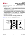
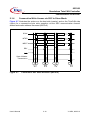
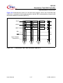
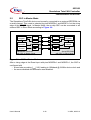
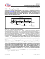
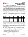
1
U se r’ s Ma n ua l, V1 .0 D 2, D ec . 20 00
8 2C 90 0
S t a n d a l o n e T w i n C AN C o n t r o l l e r
M i c ro c o n t ro l l e rs
N e v e r
s t o p
t h i n k i n g .
Edition 2000-12
Published by Infineon Technologies AG,
St.-Martin-Strasse 53,
D-81541 München, Germany
© Infineon Technologies AG 2000.
All Rights Reserved.
Attention please!
The information herein is given to describe certain components and shall not be considered as warranted
characteristics.
Terms of delivery and rights to technical change reserved.
We hereby disclaim any and all warranties, including but not limited to warranties of non-infringement, regarding
circuits, descriptions and charts stated herein.
Infineon Technologies is an approved CECC manufacturer.
Information
For further information on technology, delivery terms and conditions and prices please contact your nearest
Infineon Technologies Office in Germany or our Infineon Technologies Representatives worldwide (see address
list).
Warnings
Due to technical requirements components may contain dangerous substances. For information on the types in
question please contact your nearest Infineon Technologies Office.
Infineon Technologies Components may only be used in life-support devices or systems with the express written
approval of Infineon Technologies, if a failure of such components can reasonably be expected to cause the failure
of that life-support device or system, or to affect the safety or effectiveness of that device or system. Life support
devices or systems are intended to be implanted in the human body, or to support and/or maintain and sustain
and/or protect human life. If they fail, it is reasonable to assume that the health of the user or other persons may
be endangered.
U se r’ s Ma n ua l, V1 .0 D 2, D ec . 20 00
82 C9 00
S t a n d a lo n e T wi n C A N C o n t r o l l e r
M i c ro c o n t ro l l e rs
N e v e r
s t o p
t h i n k i n g .
82C900
Revision History:
2000-12
Previous Version:
-
Page
V1.0D2
Subjects (major changes since last revision)
We Listen to Your Comments
Any information within this document that you feel is wrong, unclear or missing at all?
Your feedback will help us to continuously improve the quality of this document.
Please send your proposal (including a reference to this document) to:
[email protected]
82C900
Standalone TwinCAN Controller
Table of Contents
Page
1
1.1
1.2
1.2.1
1.2.2
1.2.3
1.3
1.3.1
1.3.2
1.4
1.4.1
1.4.2
1.4.3
1.4.4
1.4.5
1.4.6
1.5
1.5.1
1.6
1.6.1
1.6.2
1.6.3
1.6.4
1.7
Standalone TwinCAN Device . . . . . . . . . . . . . . . . . . . . . . . . . . . . . . . . 1-1
Architectural Overview . . . . . . . . . . . . . . . . . . . . . . . . . . . . . . . . . . . . . . . 1-1
Application Fields . . . . . . . . . . . . . . . . . . . . . . . . . . . . . . . . . . . . . . . . . . . 1-3
Connection to a Host Device via the Parallel Interface . . . . . . . . . . . . 1-3
Connection to a Host Device via the Serial Interface . . . . . . . . . . . . . 1-4
Operation without Host Device . . . . . . . . . . . . . . . . . . . . . . . . . . . . . . 1-5
Pin Definitions and Functions . . . . . . . . . . . . . . . . . . . . . . . . . . . . . . . . . 1-6
Pin Configuration . . . . . . . . . . . . . . . . . . . . . . . . . . . . . . . . . . . . . . . . . 1-6
Pin Definition . . . . . . . . . . . . . . . . . . . . . . . . . . . . . . . . . . . . . . . . . . . . 1-6
Device Description . . . . . . . . . . . . . . . . . . . . . . . . . . . . . . . . . . . . . . . . . 1-10
Host Access to the CAN RAM . . . . . . . . . . . . . . . . . . . . . . . . . . . . . . 1-10
Register Addressing in Page Mode . . . . . . . . . . . . . . . . . . . . . . . . . . 1-12
Clock Generation . . . . . . . . . . . . . . . . . . . . . . . . . . . . . . . . . . . . . . . . 1-13
Power Saving Modes . . . . . . . . . . . . . . . . . . . . . . . . . . . . . . . . . . . . . 1-15
Interrupt Control . . . . . . . . . . . . . . . . . . . . . . . . . . . . . . . . . . . . . . . . . 1-16
Initialization via CAN Bus . . . . . . . . . . . . . . . . . . . . . . . . . . . . . . . . . . 1-17
Port Control Unit . . . . . . . . . . . . . . . . . . . . . . . . . . . . . . . . . . . . . . . . . . 1-18
Output Port Configuration . . . . . . . . . . . . . . . . . . . . . . . . . . . . . . . . . 1-19
Parallel Bus used as Communication Channel . . . . . . . . . . . . . . . . . . . 1-20
Parallel Bus Functions with an active SSC . . . . . . . . . . . . . . . . . . . . 1-20
Parallel Bus used as Trigger for a CAN Message Transfer . . . . . . . . 1-20
General Purpose I/O Registers accessed via CAN Bus . . . . . . . . . . 1-20
Parallel Bus used as CAN Status Monitor . . . . . . . . . . . . . . . . . . . . . 1-21
Register Address Map . . . . . . . . . . . . . . . . . . . . . . . . . . . . . . . . . . . . . . 1-23
2
2.1
2.1.1
2.1.2
2.1.3
2.1.4
2.1.5
2.2
2.2.1
2.2.2
2.3
Communication via the SSC . . . . . . . . . . . . . . . . . . . . . . . . . . . . . . . . . 2-1
SSC in Slave Mode . . . . . . . . . . . . . . . . . . . . . . . . . . . . . . . . . . . . . . . . . 2-2
Single Read Access via SSC in Slave Mode . . . . . . . . . . . . . . . . . . . . 2-4
Consecutive Read Accesses via SSC in Slave Mode . . . . . . . . . . . . . 2-7
Single Write Access via SSC in Slave Mode . . . . . . . . . . . . . . . . . . . 2-13
Consecutive Write Access via SSC in Slave Mode . . . . . . . . . . . . . . 2-16
Error Handling . . . . . . . . . . . . . . . . . . . . . . . . . . . . . . . . . . . . . . . . . . 2-21
SSC in Master Mode . . . . . . . . . . . . . . . . . . . . . . . . . . . . . . . . . . . . . . . 2-22
Communication Protocol . . . . . . . . . . . . . . . . . . . . . . . . . . . . . . . . . . 2-23
Initialization via Serial EEPROM . . . . . . . . . . . . . . . . . . . . . . . . . . . . 2-24
Configuration of the SSC . . . . . . . . . . . . . . . . . . . . . . . . . . . . . . . . . . . . 2-26
3
3.1
3.2
3.2.1
3.2.2
3.2.3
TwinCAN Module Description . . . . . . . . . . . . . . . . . . . . . . . . . . . . . . .
Overview . . . . . . . . . . . . . . . . . . . . . . . . . . . . . . . . . . . . . . . . . . . . . . . . .
TwinCAN Control Shell . . . . . . . . . . . . . . . . . . . . . . . . . . . . . . . . . . . . . .
Initialization Processing . . . . . . . . . . . . . . . . . . . . . . . . . . . . . . . . . . . .
Interrupt Request Compressor . . . . . . . . . . . . . . . . . . . . . . . . . . . . . .
Global Control and Status Logic . . . . . . . . . . . . . . . . . . . . . . . . . . . . .
User’s Manual
I-1
3-1
3-1
3-4
3-4
3-5
3-5
V1.0D2, 2000-12
82C900
Standalone TwinCAN Controller
Table of Contents
Page
3.3
3.3.1
3.3.2
3.3.3
3.3.4
3.3.5
3.3.6
3.3.7
3.4
3.4.1
3.4.2
3.4.3
3.4.4
3.4.5
3.5
3.5.1
3.5.2
3.6
3.6.1
3.6.2
3.6.3
3.7
3.7.1
3.7.2
3.7.3
CAN Node Control Logic . . . . . . . . . . . . . . . . . . . . . . . . . . . . . . . . . . . . . 3-6
Overview . . . . . . . . . . . . . . . . . . . . . . . . . . . . . . . . . . . . . . . . . . . . . . . 3-6
Timing Control Unit . . . . . . . . . . . . . . . . . . . . . . . . . . . . . . . . . . . . . . . 3-8
Bitstream Processor . . . . . . . . . . . . . . . . . . . . . . . . . . . . . . . . . . . . . 3-10
Error Handling Logic . . . . . . . . . . . . . . . . . . . . . . . . . . . . . . . . . . . . . 3-10
Node Interrupt Processing . . . . . . . . . . . . . . . . . . . . . . . . . . . . . . . . . 3-11
Message Interrupt Processing . . . . . . . . . . . . . . . . . . . . . . . . . . . . . . 3-12
Interrupt Indication . . . . . . . . . . . . . . . . . . . . . . . . . . . . . . . . . . . . . . 3-12
Message Handling Unit . . . . . . . . . . . . . . . . . . . . . . . . . . . . . . . . . . . . . 3-14
Arbitration and Acceptance Mask Register . . . . . . . . . . . . . . . . . . . . 3-15
Handling of Remote and Data Frames . . . . . . . . . . . . . . . . . . . . . . 3-16
Handling of Transmit Message Objects . . . . . . . . . . . . . . . . . . . . . . . 3-17
Handling of Receive Message Objects . . . . . . . . . . . . . . . . . . . . . . . 3-20
Single Data Transfer Mode . . . . . . . . . . . . . . . . . . . . . . . . . . . . . . . 3-22
CAN Message Object Buffer (FIFO) . . . . . . . . . . . . . . . . . . . . . . . . . . . 3-23
Buffer Access by the CAN Controller . . . . . . . . . . . . . . . . . . . . . . . . . 3-24
Buffer Access by the CPU . . . . . . . . . . . . . . . . . . . . . . . . . . . . . . . . . 3-26
Gateway Message Handling . . . . . . . . . . . . . . . . . . . . . . . . . . . . . . . . . 3-26
Normal Gateway Mode . . . . . . . . . . . . . . . . . . . . . . . . . . . . . . . . . . . 3-27
Normal Gateway with FIFO Buffering . . . . . . . . . . . . . . . . . . . . . . . . 3-31
Shared Gateway Mode . . . . . . . . . . . . . . . . . . . . . . . . . . . . . . . . . . . 3-34
Programming the TwinCAN Module . . . . . . . . . . . . . . . . . . . . . . . . . . . 3-38
Configuration of CAN Node A/B . . . . . . . . . . . . . . . . . . . . . . . . . . . . 3-38
Initialization of Message Objects . . . . . . . . . . . . . . . . . . . . . . . . . . . . 3-38
Controlling a Message Transfer . . . . . . . . . . . . . . . . . . . . . . . . . . . . . 3-39
4
4.1
4.2
4.3
4.4
Standalone Shell Register Description . . . . . . . . . . . . . . . . . . . . . . . . 4-1
Register Map . . . . . . . . . . . . . . . . . . . . . . . . . . . . . . . . . . . . . . . . . . . . . . 4-1
Control Registers . . . . . . . . . . . . . . . . . . . . . . . . . . . . . . . . . . . . . . . . . . . 4-3
Port Registers . . . . . . . . . . . . . . . . . . . . . . . . . . . . . . . . . . . . . . . . . . . . 4-16
Interrupt Register . . . . . . . . . . . . . . . . . . . . . . . . . . . . . . . . . . . . . . . . . . 4-21
5
5.1
5.2
5.3
5.4
TwinCAN Register Description . . . . . . . . . . . . . . . . . . . . . . . . . . . . . . . 5-1
Register Map . . . . . . . . . . . . . . . . . . . . . . . . . . . . . . . . . . . . . . . . . . . . . 5-1
CAN Node A / B Registers . . . . . . . . . . . . . . . . . . . . . . . . . . . . . . . . . . . . 5-4
CAN Message Object Registers . . . . . . . . . . . . . . . . . . . . . . . . . . . . . . 5-21
Global CAN Control / Status Registers . . . . . . . . . . . . . . . . . . . . . . . . . 5-35
6
Index . . . . . . . . . . . . . . . . . . . . . . . . . . . . . . . . . . . . . . . . . . . . . . . . . . . . 6-1
User’s Manual
I-2
V1.0D2, 2000-12
82C900
Standalone TwinCAN Controller
Standalone TwinCAN Device
1
Standalone TwinCAN Device
1.1
Architectural Overview
The Standalone TwinCAN device provides several submodules to control the data flow
and to configure the peripheral function:
• Two interface channels are implemented for the communication with a host device:
– the Multiplexed Data/Address Bus can be used by an external CPU to read and
write the TwinCAN’s internal registers for initial configuration and control during
normal operation. The standard Infineon Bus Mode and the Motorola Bus Mode can
be handled.
– alternatively, a Synchronous Serial Channel (SSC) may be selected to read out the
initial TwinCAN’s register configuration from a serial EEPROM. The SSC can be
also used by an external control device (microcontroller, CPU, etc.) in order to
exchange control and status information.
• Both communication channels are based on byte transfers. In order to minimize the
communication overhead, all internal 16-bit and 32-bit wide registers can be accessed
in Page Mode requiring only one address byte.
• Powerful initialization mechanism for all registers, the device can be configured via
EEPROM, based on CAN messages or by an external host device.
• Additional input/output functionality controlled by CAN messages. The transmission of
CAN messages can be triggered by input pins if the SSC is used for communication.
• The clock control unit can be supplied with an external clock. Alternatively, an on-chip
oscillator may be used to generate a clock driving also an external device via an output
pin.
• Power Saving features have been implemented. A Sleep Mode and a Power-Down
Mode can be activated in order to minimize the power consumption. The clock control
of the device can be controlled by CAN messages.
• The internal power saving status can be monitored at output pins. This allows flexible
and powerful system partitioning.
• The Device Controller unit generates the internal target address by concatenating the
contents of the PAGE register with the address delivered by the appropriate host read/
write access.
• The Interrupt Control unit passes the interrupt requests generated by the TwinCAN
controller to the external host via selectable output pins.
• The Port Control unit can be used to select the required functionality of the port pins
operating as communication channel, CAN node function monitor, interrupt request
line or general purpose I/O. Furthermore, the slew rate of pins configured for output
operation can be adjusted via this module.
User’s Manual
1-1
V1.0D2, 2000-12
82C900
Standalone TwinCAN Controller
Standalone TwinCAN Device
The TwinCAN module permits the connection and autonomous handling of two
independent CAN buses.
• Full-CAN module with 32 message objects, which can be independently assigned to
one of the two buses.
• The CAN protocol version 2.0B active with standard and extended identifiers can be
handled.
• The full CAN baudrate range is supported.
• Scalable FIFO mechanism for reception and transmission in order to improve the realtime behavior of the system.
• Built-in automatic gateway functionality for data exchange between both CAN buses.
The gateway feature can also be used for automatic reply to received messages
(lifesign: “I got it!”).
• Powerful interrupt structure, permitting application-specific interrupt generation.
• Remote frames can be monitored.
• Enhanced acceptance filtering (an acceptance mask for each message object).
• A 16-bit frame count / timestamp is implemented for each message object.
• Analyzing mode (no dominant level will be sent) supported.
Figure 1-1 shows a block diagram of the 82C900 device architecture.
4
CTRL0..CTRL3
8
Port
Control
CAN
data
P0..P7
2
MODE0, MODE1
Interrupt
Control
int
Clock
control
clk
2
OUT0, OUT1
2
XTAL1, XTAL2
addr
2
RESET, RDY
SSC
2
data
CAN CAN
Node Node
A
B
Message
Object
Buffer
RXDCA, RXDCB
2
TXDCA, TXDCB
Figure 1-1
Device Control
TwinCAN Control
Standalone TwinCAN Architecture
Note: The CAN bus transceivers are not integrated and have to be connected externally.
User’s Manual
1-2
V1.0D2, 2000-12
82C900
Standalone TwinCAN Controller
Standalone TwinCAN Device
1.2
Application Fields
The Standalone TwinCAN device 82C900 can be used in application requiring one or
two independent CAN nodes. The built-in FIFO and gateway features minimize the CPU
load for the message handling and lead to an improved real-time behavior. The access
to the internal registers can be handled via a parallel or a serial interface, adapted to a
large variety of applications. The interface selection is done via the two MODE pins,
which can be directly connected to the supply voltage or via pull-up/down resistors (of
about 10-47 kOhm). In all modes, the clock generation can be controlled either by the
82C900 device or by the system it is connected to.
1.2.1
Connection to a Host Device via the Parallel Interface
The 82C900 can be connected to a host device via a parallel 8-bit multiplexed interface.
Therefore, pin MODE0 has to be 0, whereas pin MODE1 selects, whether an Infineon(Intel-) compatible or an Motorola-compatible protocol is handled. In this mode, the
device can be easily used to extend the CAN capability of a system. The internal
registers can be accessed in pages of 256 bytes per page. An additional RDY output
indicates when the device is ready to be accessed. This signal can be used to detect an
overload situation of the CAN device (too many host accesses to the TwinCAN module).
One interrupt output line (OUT1) is always available, a second one (OUT0) can be used
as clockout pin or as another interrupt output.
C A N B us A
C A N B us B
T ran sceiver
Tra nsce ive r
RXDCA,
TXDCA
RXDCB,
TXDCB
82C 900
Tw inC A N M odu le
C lock C ontrol
P arallel Interface
Interrup t
C on tro l
A D 7 ..0
C T R L 3 ..0
RDY
O UTx
H ost
Figure 1-2
User’s Manual
Host Connection via the Parallel Interface
1-3
V1.0D2, 2000-12
82C900
Standalone TwinCAN Controller
Standalone TwinCAN Device
1.2.2
Connection to a Host Device via the Serial Interface
The second possibility to connect the 82C900 to a host device is via the serial interface.
This mode is selected if the pin MODE0=1 and MODE1=0.
The standard four-line SPI-compatible interface has been extended by a RDY signal,
which indicates that the serial interface is ready for the next access by the host.
The page size is reduced to 128 bytes per page, because the MSB of the address byte
contains a read/write indication. A special incremental access mode has been
implemented in order to reduce significantly the number of transferred bytes for
consecutive register accesses.
The 8 remaining I/O pins from the unused parallel interface are controlled by a port
control logic and can be used as I/O extension. These lines can be read or written by the
serial channel or by CAN messages. Furthermore, these lines can be programmed as
additional interrupt output lines in order to increase the number of independent
interrupts.
The output lines OUT0 and OUT1 have the same functionality in the case a parallel
interface or a serial interface connects the 82C900 to a host device.
C A N B us A
C A N B us B
T ran sceiver
T ransceiver
RXDCA,
TXDCA
RXDCB,
TXDCB
8 2C 900
Tw in C A N M od ule
P ort C on trol
I/O 7 ..0
S erial Interface
C T R L 3 ..0
In put/O utput
E xte nsio n
Figure 1-3
User’s Manual
C lo ck C ontrol
In te rrup t
C ontrol
RDY
OUTx
H o st
Host Connection via the Serial Interface
1-4
V1.0D2, 2000-12
82C900
Standalone TwinCAN Controller
Standalone TwinCAN Device
1.2.3
Operation without Host Device
The standalone functionality comprises an additional mode, leading to a low-cost
system, which does not require any external host device. This mode can be selected by
setting the input pins MODE0 and MODE1 to 1. The best solution are pull-up resistors
(about 10 to 47 kOhm). After the reset phase, the MODE pins can be enabled to control
the power-down functionality of the entire connected system by indicating the internal
status of two clock control bits. The power-down functionality can run completely via
CAN messages (sleep and wake-up by CAN messages).
The initialization sequence is automatically started from an external non-volatile
memory, a serial (SPI-compatible) EEPROM. The data, which is read out from the
EEPROM permits the user to initialize the registers with the desired values in a freely
programmable order. Changes in the application only lead to modified data stored in the
non-volatile memory.
For example, the bit timing, one message object and some control registers are set up
via the data read from the EEPROM. Then, the initialization can continue via CAN
messages.
The 8 remaining I/O pins from the unused parallel interface are controlled by a port
control logic and can be used as I/O extension. These lines can be read or written by
CAN messages.
C A N B us A
C A N B us B
T ransceiver
T ran sce iver
RXDCA,
TXDCA
RXDCB,
TXDCB
8 2C 900
Tw inC A N M o dule
P ort C on tro l
I/O 7 ..0
Inp ut/O u tpu t
e xte nsion
Figure 1-4
User’s Manual
C lock C ontrol
S eria l Interface
D evice
C on tro l
C T R L 3 ..0
S e rial
EEPROM
P o w er-D ow n
Indication
Connection to a Serial EEPROM
1-5
V1.0D2, 2000-12
82C900
Standalone TwinCAN Controller
Standalone TwinCAN Device
1.3
Pin Definitions and Functions
1.3.1
Pin Configuration
RXDC A
TXDC A
RESET
X TA L 1
X TA L 2
OUT0
VDD
VSS
CTRL0
CTRL2
P0
P2
P4
P6
Figure 1-5
1.3.2
1
2
3
4
5
6
7
8
9
10
11
12
13
14
28
27
26
25
24
23
22
21
20
19
18
17
16
15
RXDCB
TXDC B
MODE0
MODE1
RDY
OUT1
VD D
VSS
CTRL1
CTRL3
P1
P3
P5
P7
82C900 Pin Configuration
Pin Definition
Table 1-1
Pin Definitions and Functions
Symbol
Pin
I/O 1) Function
Number
RXDCA
1
I
Receiver Input of CAN Node A
Receiver input of CAN node A, connected to the
associated CAN bus via a transceiver device.
TXDCA
2
O
Transmitter Output of CAN Node A
TXDCA delivers the output signal of CAN node A. The
signal level has to be adapted to the physical layer of the
CAN bus via a transceiver device.
RXDCB
28
I
Receiver Input of CAN Node B
Receiver input of CAN node B, connected to the
associated CAN bus via a transceiver device.
User’s Manual
1-6
V1.0D2, 2000-12
82C900
Standalone TwinCAN Controller
Standalone TwinCAN Device
Table 1-1
Pin Definitions and Functions (cont’d)
Symbol
Pin
I/O 1) Function
Number
TXDCB
27
O
Transmitter Output of CAN Node B
TXDCB delivers the output signal of CAN node B. The
signal level has to be adapted to the physical layer of the
CAN bus via a transceiver device.
RESET
3
I
Reset
A low level on this pin resets the device.
RDY
24
O
Ready Signal
Output signal indicating that the standalone device is
ready for data transfer.
CTRL0
9
I/O
Control 0
MODE0=0: Chip Select CS
Input used as Chip Select for the device.
MODE0=1: Select Slave SLS
MODE1=0: Input used to enable SSC action when
active.
MODE1=1: Output used to select a slave when active.
CTRL1
20
I/O
Control 1
MODE0=0:
Address Latch Enable or Address
Strobe, ALE or AS
Input used for latching the address from the multiplexed
address/data bus.
MODE0=1: Serial Channel Clock SCLK
Input/output of the SSC clock.
MODE1=0: Clock input
MODE1=1: Clock output
CTRL2
User’s Manual
10
I/O
Control 2
MODE0=0:
MODE1=0:
MODE1=1:
MODE1=1:
MODE0=1:
MODE1=0:
MODE1=1:
Write or Read/Write, WR or R/W
Input used as write signal WR
R/W=0: Data transfer direction = write
R/W=1: Data transfer direction = read
Master Transmit Slave Receive MTSR
Serial data input
Serial data output
1-7
V1.0D2, 2000-12
82C900
Standalone TwinCAN Controller
Standalone TwinCAN Device
Table 1-1
Pin Definitions and Functions (cont’d)
Symbol
Pin
I/O 1) Function
Number
CTRL3
19
P7
P6
P5
P4
P3
P2
P1
P0
I/O
Control 3
MODE0=0:
MODE1=0:
MODE1=0:
MODE0=1:
MODE1=0:
MODE1=1:
Read or Read/Write Enable, RD or E
Input used as read signal RD
Read/write enable
Master Receive Slave Transmit MRST
Serial data output
Serial data input
15
14
16
13
17
12
18
11
I/O
Parallel Bus
MODE0=0: 8-bit Address/ Data Bus AD[7:0]
Address and data bus AD7..AD0 in 8-bit multiplexed
modes.
MODE0=1: 8-bit parallel I/O Port IO[7:0]
Programmable 8-bit general purpose I/O-port IO7..IO0.
6
O
Output Line 0
The logic “0“ level at this pin indicates an interrupt request
to the external host device if selected as interrupt output.
The interrupt line will be active if there is a new pending
interrupt request for interrupt node 0 (according to
register GLOBCTR).
If selected as clock output, the functionality is defined by
register CLKCTR.
OUT1
23
O,
Output Line 1
open The logic 0 level at this pin indicates an interrupt request
drain to the external host device.
The interrupt line will be active if there is a new pending
interrupt request for interrupt node 1 (according to
register GLOBCTR).
MODE0 3)
26
I/O, Interface Selection
open Pin MODE0 selects whether the on-chip SSC or an 8-bit
drain multiplexed bus are used to access the TwinCAN device.
MODE0=0: 8-bit multiplexed address/data bus
MODE0=1: on-chip SSC
After registering the initial state of MODE0 with the rising
edge of the reset signal, the respective pin can be used
as additional general purpose or special function I/O line
according register IOMODE4.
OUT0
2)
User’s Manual
1-8
V1.0D2, 2000-12
82C900
Standalone TwinCAN Controller
Standalone TwinCAN Device
Table 1-1
Pin Definitions and Functions (cont’d)
Symbol
Pin
I/O 1) Function
Number
MODE1
25
I/O, Interface Mode Selection
open Pin MODE1 determines the access mode of the host
drain device.
MODE0=0: 8-bit multiplexed bus
MODE1=0: Infineon / Intel mode, (RD, WR)
MODE1=1: Motorola mode, (R/W, E)
MODE0=1: On-chip SSC
MODE1=0: SSC is slave, host device is master
MODE1=1: SSC is master, external serial
EEPROM is slave
After registering the initial state of MODE1 with the rising
edge of the reset signal, the respective pin can be used
as additional general purpose or special function I/O line
according register IOMODE4.
XTAL1
4
I
XTAL1
Input of the inverting oscillator amplifier and input to the
internal clock generation circuit.
When the 82C900 device is provided with an external
clock, XTAL1 should be driven while XTAL2 is left
unconnected.
Minimum and maximum high and low pulse width as well
as rise/fall times specified in the AC characteristics must
be respected.
XTAL2
5
O
XTAL2
Output of the inverting oscillator amplifier.
VSS
21, 8
0V
Ground, both pins must be connected.
VDD
22, 7
+5V
Power Supply, both pins must be connected.
1)
The slew rate of the output pins OUT0, OUT1, CTRL1..3, P0..P7, TXDCA and TXDCB can be defined by the
bit fields SLR0..3 in register GLOBCTR.
2)
After reset, this pin is configured as clock output, see register CLKCTR.
3)
The initial logic state on pins MODE0 and MODE1 is registered with the rising edge of the RESET input.
Afterwards, both pins can be used as additional I/O lines, according to functionality specified in register
IOMODE4.
User’s Manual
1-9
V1.0D2, 2000-12
82C900
Standalone TwinCAN Controller
Standalone TwinCAN Device
1.4
Device Description
1.4.1
Host Access to the CAN RAM
The internal CAN message objects and the CAN control registers are located in a RAM
area, the CAN RAM. It is has one access port, which has to be shared by the TwinCAN
controller and the bus interface to the external communication channels (Figure 1-6).
The registers located in the CAN RAM area are indicated by 32-bit reset values.
CAN Controller
Address Decoder
CAN
Buses
CAN RAM
Output Register
8-bit Mux
Bus
Interface
...
SSC
Access Arbiter
Figure 1-6
Control / Status bits
in SFRs, e.g. for
SSC, system
control, etc.
Internal CAN RAM Access
In order to avoid collisions, an access arbiter is implemented. If the TwinCAN controller
is accessing the RAM while one of the external communication channels wants to read
or write to the RAM, the current access must be correctly finished before allowing the
next one. As a consequence, the bus interface might have to wait until the TwinCAN
controller has finished its access.
In the case that the Serial Communication Channel (SSC) has been selected to access
the Standalone TwinCAN device, this problem has been solved by implementing a
handshake mechanism based on a RDY (ready) signal.
If the parallel bus interface has been selected, the access is only allowed while RDY=1
and the following rules have to be respected:
For host devices, which do not support an extended access cycle time by introducing
wait states, an output buffer register has been implemented. This output buffer register
delivers the data for all read accesses of the host communication channel to the internal
CAN RAM. A RAM read operation to the desired address starts an internal read access
in the CAN RAM area returning the required data to the output buffer register. A second
read access to the internal RAM will deliver the requested data buffered in the output
register. This structure permits the user to read data from the internal RAM area with two
consecutive short read operations. Between these two read operations, further
User’s Manual
1-10
V1.0D2, 2000-12
82C900
Standalone TwinCAN Controller
Standalone TwinCAN Device
instructions may be executed by the external host CPU. In order to read four bytes from
the CAN RAM, five read accesses are required (n bytes -> n+1 read accesses).
The control bit LAE (long read enable) in register GLOBCTR defines whether the CAN
RAM output register can be updated while the read access via the host communication
channel is in progress. For host devices, supporting long access cycles by introducing
wait states, LAE should be set to 1, which allows an update of the CAN RAM output
buffer register during a running host read operation (Figure 1-7). LAE = 0 prevents a
modification of the RAM output buffer register during a host read operation and should
be selected for host devices with short read access cycle time. A write operation to the
internal RAM is handled by an internal buffer structure. As a result, only one short write
access is required.
Old data
New data
Data is read
by host
Long host
read cycle
Data is stored in
buffer register
Triggers read
access in RAM
RAM read operation
Triggers read
access in RAM
Figure 1-7
Data is stored in
buffer register
1st short read
2nd short read
Old data
New data
Data is read
by host
Short host
read cycle
CAN RAM Read Access
When bit LAE is set to 0 (short read access), a data loss may occur, if an application
program is suspended by an interrupt service routine between both consecutive short
read accesses to the internal CAN RAM of the TwinCAN device. In order to guaranty
data consistency, the interrupt service routine has to buffer the address of the last CAN
RAM read access stored in the LRA bit field of the CAN address buffer register CAB. At
the end of the interrupt routine, a (dummy) read access to the target address buffered
before should be programmed to ensure that the data in the CAN RAM output register
fits to the address of the last read access from the internal CAN RAM before the interrupt
routine has been started.
Registers, which are not located in the CAN RAM area are indicated by 16-bit reset
values and can be accessed by single short read or write actions.
User’s Manual
1-11
V1.0D2, 2000-12
82C900
Standalone TwinCAN Controller
Standalone TwinCAN Device
Note: The explicit short and long access timings are given in the Data Sheet.
1.4.2
Register Addressing in Page Mode
The input pin MODE0 (registered at the rising edge of the RESET signal) defines
whether a serial or a parallel communication channel (SSC=SPI-compatible or 8-bit
multiplexed bus) is used to exchange data with an external host devices. The complete
address for an internal register access is 11 bit long and contains two parts. The upper
part defines a page and the lower part is given by the host access. Depending on the
selected communication channel, the page size is 128 bytes (SSC, bit 7 is used as read/
write indication) or 256 bytes (8-bit multiplexed address/data bus).
The 11 bit internal target address is given by a concatenation of the contents of two
registers:
• the upper bits of the target address are provided by the internal page register (PAGE),
• the lower address bits are delivered via the SSC or the multiplexed address/data bus
and are stored in an address register.
Address Generation in 8-bit Multiplexed Bus Mode
x
x
x
x
A10 A9
A8
x
8 bit Mux. Bus
Page Register
A7
A6
A5
A4
A3
A2
A1
A0
A2
A1
A0
A2
A1
A0
A1
A0
Host Address
A10 A9
A8
A7
A6
A5
A4
A3
Target Address
Address Generation in SSC Mode
x
SSC
x
x
x
x
A10 A9
A6
A5
A4
A3
Host Address
A8
A7
A8
A7
Page Register
A10 A9
A6
A5
A4
A3
A2
Target Address
A10..A8 A7
A6..A0
Figure 1-8
User’s Manual
Paged Addressing Scheme
1-12
V1.0D2, 2000-12
82C900
Standalone TwinCAN Controller
Standalone TwinCAN Device
1.4.3
Clock Generation
The TwinCAN device is provided with an on-chip oscillator (pins XTAL1, XTAL2), which
may be used to generate a system clock. For this purpose, a clock divider and a clock
output pin have been integrated in order to support external devices with a lower working
frequency. A clock division factor of 1, 2 or 4 can be adjusted via bit field CLKDIV in
register CLKCTR. This feature enables the TwinCAN device to run internally with 24
MHz for CAN operation while the external device (e.g. 8-bit controller with 12MHz) is
provided with a prescaled clock. Pin OUT0 can be configured via control bit SELOUT0
in register GLOBCTR to output the divided clock signal.
Oscillator
SELOUT0=00B
Crystal
Clock Divider
OUT0
Clock Generation
Interrupt
Generation
OUT1
Host Interface
Slave Interface
Standalone TwinCAN
Figure 1-9
Iinterrupt System
Host
System Clock Generation by TwinCAN Device
The system clock may be also generated by an external device operating at the same
frequency like the Standalone TwinCAN device. In this case, the TwinCAN’s on-chip
oscillator is switched off and the output line OUT0 can be programmed as interrupt
output.
User’s Manual
1-13
V1.0D2, 2000-12
82C900
Standalone TwinCAN Controller
Standalone TwinCAN Device
Oscillator
Crystal
SELOUT0=01B
Clock Divider
OUT0
Clock Generation
Interrupt
Generation
OUT1
Host Interface
Slave Interface
Standalone TwinCAN
Figure 1-10
Interrupt System
Host
System Clock Generation by an External Device
Another alternative is the use of two independent crystals. In this case, OUT0 may be
also configured as interrupt output.
Oscillator
Crystal
SELOUT0=01B
Crystal
Clock Divider
OUT0
Clock Generation
Interrupt
Generation
OUT1
Host Interface
Slave Interface
Standalone TwinCAN
Figure 1-11
User’s Manual
Interrupt System
Host
Clock Generation by Independent Clock Sources
1-14
V1.0D2, 2000-12
82C900
Standalone TwinCAN Controller
Standalone TwinCAN Device
1.4.4
Power Saving Modes
In order to reduce power consumption, the system clock of the TwinCAN device can be
gated off via control bits CANCLK (CAN clock) and PWD (power down) in register
CLKCTR (clock control). Three operating modes have been implemented:
Normal Mode (PWD=0, CANCLK=1):
The oscillator is running and the TwinCAN device is clocked (reset value).
Sleep Mode (PWD=0, CANCLK=0):
The oscillator is running, but the TwinCAN module, the SSC and the 8-bit port logic are
gated off. The wake-up processing can be initiated by a falling edge on one of the input
pins RXDCA, RXDCB (if enabled by control bits CANAWU, CANBWU), RESET or an
activation of CS or SLS, respectively. The CAN output pins become recessive. The
clockout signal at pin OUT0 (if selected by bit field SELOUT0) is still available.
Power Down Mode (PWD=1, CANCLK=x):
Oscillator is stopped and the TwinCAN device is gated off. The CAN output pins become
recessive. The clockout signal (if enabled) is stopped.
An activation of the RESET input is required to wake-up the TwinCAN device again.
C LK D IV
O U T0
SE L O U T 0
O scilla tor
D isa b le
clo ck
Tw inC A N
M od ule
PW D
RXDCA
RXDCB
RESET
C S , S LS
Figure 1-12
SSC
W ake-up
C o ntrol
C ANC LK
8-b it IO
P ort
Power Saving Mode and Wake-up Functionality
The power saving modes may be also entered upon a CAN message received by a
predefined message object, if enabled by control bit SLPEN in register CANPWD. The
number of the respective message object is defined via bit field SLPMSG. The selected
message object has to be configured for receive operation and works independently of
the respective MSGVAL value. Data byte 0 of the received CAN message is treated as
authorization code, which has to match the contents of bit field SLPCODE in order to
enable the required power saving mode.
User’s Manual
1-15
V1.0D2, 2000-12
82C900
Standalone TwinCAN Controller
Standalone TwinCAN Device
1.4.5
Interrupt Control
An interrupt request, generated by one of the 8 TwinCAN’s interrupt nodes, can be
indicated by output pins OUT0 and OUT1 or by the parallel I/O bus.
When bit field SELOUT0 (select output 0) in register GLOBCTR (global control) is set to
01B, output pin OUT0 is enabled to report an interrupt request. If control bit INTGR0
(interrupt group 0) is reset, only a request from interrupt node 0 is reported via output
OUT0. If INTGR0 is set to 1, all interrupt requests generated by interrupt node 0, 2, 4
and 6 are indicated via OUT0 and the external software has to identify the interrupt
request source by analyzing the interrupt control register INTCTR and the interrupt
pending registers AIR/BIR of the TwinCAN module. Depending on control bit INTGR1,
output pin OUT1 reports only an interrupt request generated by interrupt node 1 or
indicates all interrupt requests from interrupt node 1, 3, 5 and 7.
When the SSC is used as communication channel, the 8 pins of the parallel I/O bus can
be configured by bit fields IOM0..IOM7 in register IOMODE0/2 to report the interrupt
requests generated by the 8 interrupt nodes. This report source operates parallel to the
interrupt request indication via pins OUT0 or OUT1.
Register INTCTR indicates via flag INTi (i=0-7), which interrupt node has been activated.
An interrupt request flag INTi can be cleared by setting the corresponding INTRi bit in
register INTCTR to 1. Bit INTRi is automatically reset by hardware after bit INTi has been
cleared. Interrupt requests are generated at the interrupt output lines even if the
corresponding INTi flag is still set and has not been reset by software before (INTi only
for indication purpose).
The interrupt pulse driven by the selected interrupt output pin will have a length of 5
oscillator periods (TCAN).
User’s Manual
1-16
V1.0D2, 2000-12
82C900
Standalone TwinCAN Controller
Standalone TwinCAN Device
1.4.6
Initialization via CAN Bus
If the initialization of the Standalone TwinCAN device has been started via the SSC in
Master Mode, the instructions read in from an external serial EEPROM may be used to
set control bit INITEN (initialization enable) in register CANINIT (CAN initialization
control) to 1 and to reset bit field IB3 (instruction byte 3) in register INITCTR (initialization
control). In this case, the 82C900 can be reconfigured by the reception of CAN
messages. For this purpose, bit field INITMSG in register CANINIT defines the number
of the receive message object used for the import of configuration data.
The utilization of the received bytes in the message object’s data field (object number n,
n=0-31) is predefined as illustrated in Figure 1-13.
Autorisation
INIT
CODE
DBn0
Figure 1-13
Address Part
(2 bytes)
Data part
(1 to 4 bytes)
ADH
ADL
D0
D1
D2
D3
DBn1
DBn2
DBn3
DBn4
DBn5
DBn6
Structure of the Configuration Protocol via CAN Bus
In order to avoid unintended register accesses, the first transferred byte (DBn0) contains
an authorization code. When a message is received with data byte 0 matching the value
of bit field INITCODE in register CANINIT, data bytes 1 and 2 are interpreted as target
address while data bytes 3 to 6 (according to bit field DLC in register MSGCFG, minimum
DLC=4) are copied to the appropriate target address. Afterwards, all data bytes of the
referenced receive message object are overwritten with the value of 00H.
User’s Manual
1-17
V1.0D2, 2000-12
82C900
Standalone TwinCAN Controller
Standalone TwinCAN Device
1.5
Port Control Unit
Pin MODE0 selects whether the on-chip SSC or the 8-bit I/O bus interface is used as
communication channel. A logic 0 level during a rising edge on the RESET input pin
enables the 8 general purpose I/O lines in a “multiplexed data/address bus mode” while
a logic 1 level activates the SSC.
The logic state of pin MODE1 during a rising edge on the RESET pin determines the
access mode:
• If the multiplexed address/data bus interface is selected:
– MODE1=0 enables an access control with two separate RD, WR signals,
– MODE1=1 activates an access control with a R/W and a Read-Write-Enable signal.
• If the SSC is selected:
– MODE1=0 configures the on-chip SSC as slave device, which requires an external
SSC in master mode as communication partner (host device),
– MODE1=1 sets up the on-chip SSC as master device, which needs an external
SSC in slave mode as opposite terminal (serial EEPROM).
After latching the initial states of MODE0 and MODE1 with the rising edge of the reset
signal, both pins can be used as regular I/Os (open drain output) with a functionality
determined via bit fields IOM8 and IOM9 in register IOMODE4.
Depending on the selected communication channel, the pins CTRL0...CTRL3 are used
for control, status or data transmission as illustrated in Table 1-2:
Table 1-2
Functionality of the CTRL Pins
Functionality
of Pin
if Multiplex Address/Data Bus
activated
(MODE0 = 0)
if SSC enabled
(MODE0 = 1)
CTRL0
CS
Chip Select
SLS
Slave Select
CTRL1
ALE / AS
Address Latch Enable or
Address Strobe:
Input used for latching the
address from the mux. bus
SCLK
SSC Clock,
MODE1=0: input
MODE1=1: output
CTRL2
WR or
R/W
Write or Read/Write:
MTSR Master Transmit,
MODE1=0: write signal
Slave Receive Data
WR
MODE1=0: input
MODE1=1: R/W = 0: write
MODE1=1: output
R/W = 1: read
User’s Manual
1-18
V1.0D2, 2000-12
82C900
Standalone TwinCAN Controller
Standalone TwinCAN Device
Table 1-2
Functionality of the CTRL Pins (cont’d)
Functionality
of Pin
if Multiplex Address/Data Bus
activated
(MODE0 = 0)
CTRL3
RD / E
P7..P0
Address and data bus AD7..AD0 in 8bit multiplexed mode.
1.5.1
if SSC enabled
(MODE0 = 1)
Read / Read-Write Enable: MRST Master Receive,
MODE1=0: RD signal
Slave Transmit Data:
MODE1=1: Read-Write
MODE1=0: output
Enable
MODE1=1: input
Programmable 8-bit general
purpose I/O-port IO7..IO0.
The functionality of each port pin
can be individually configured via
bit fields IOM7.. IOM0 in registers
IOMODE0/2.
Output Port Configuration
All port pins, configured for output operation, are provided with a slew rate control. The
switching characteristic of output pins clustered to groups can be configured to a fast
edge or a reduced edge via bit fields SLR0..SLR3 in control register GLOBCTR.
If pin OUT0 is configured as interrupt output via bit field SELOUT0 in register GLOBCTR,
a logic 0 level indicates an interrupt request to the external host device. The interrupt line
will be active if there is a new pending interrupt request for interrupt node 0 according to
the selection made by control bit INTGR0 in register GLOBCTR. If pin OUT0 is activated
as clock output, the functionality is defined by register CLKCTR.
A logic 0 level at pin OUT1 indicates an interrupt request to the external host device. The
interrupt line will be active if there is a new interrupt request for interrupt node 1
according to the selection made by control bit INTGR1 in register GLOBCTR.
User’s Manual
1-19
V1.0D2, 2000-12
82C900
Standalone TwinCAN Controller
Standalone TwinCAN Device
1.6
Parallel Bus used as Communication Channel
If the parallel bus was selected as the communication channel, the I/O lines are
configured as an 8-bit multiplexed address/data bus. Depending on the initial state of the
MODE1 pin, the I/O bus can be adapted to interface with an Infineon or Motorola
compatible microcontroller.
The address byte occurring first on the multiplexed bus, is indicated by signal ALE or AS,
respectively. The following data byte is announced by an appropriate write or read signal
(RD, WR or R/W, E).
When the 8-bit multiplexed address/data bus has been activated, the Shell configuration
registers IOMODEx and CANIO are not taken into account.
After reset, the access to the standalone device must not start before the RDY pin
becomes active. The device should not be accessed while the RDY pin is not active.
1.6.1
Parallel Bus Functions with an active SSC
If the SSC is used as the communication channel, each pin of the 8-bit parallel bus
(P7..P0) can be individually configured as general purpose or special function input/
output via registers IOMODE0 and IOMODE2.
1.6.2
Parallel Bus used as Trigger for a CAN Message Transfer
When IOM3..IOM0 are loaded with 0001B, a falling edge detected on pin P3..P0
generates a message transfer via the CAN bus by setting control bit TXRQ in register
MSGCTR3..MSGCTR0 to 10B. If the respective message object is configured for
transmit operation, a data frame will be transmitted. A configuration as receive message
object causes a remote frame to be sent out after a falling edge has been detected at the
corresponding pin.
1.6.3
General Purpose I/O Registers accessed via CAN Bus
The pins of the 8-bit parallel bus can be configured as a general purpose I/O port by
setting bit field IOMx to 0000B or 1000B. The logical pin state is written to register INREG
or read from register OUTREG. The Standalone TwinCAN device allows access to the
INREG and OUTREG registers via the CAN bus.
The message object, used to modify register OUTREG, is selected by bit field OUTMSG
in register CANIO and has to be configured as a receive object. If control bit CANOUTEN
is set to 1, OUTREG is updated with data byte 0 of a correctly received data frame.
The message object, used to monitor register INREG, is defined by bit field INMSG in
register CANIO and has to be configured as a transmit object. If control bit CANINEN is
set to 1, the contents of INREG is transmitted via data byte 0 of an appropriate data
frame, when TXRQ of the respective message object is set to 10B (e.g. by a matching
remote frame).
User’s Manual
1-20
V1.0D2, 2000-12
82C900
Standalone TwinCAN Controller
Standalone TwinCAN Device
1.6.4
Parallel Bus used as CAN Status Monitor
The I/O lines may be programmed to monitor the internal status of the TwinCAN
controller during a message transfer:
• Four CAN status lines (CD1A, CD0A, CD1B, CD0B) may be used to indicate, which
part of a data/remote/error frame is currently transferred via TwinCAN node A and
TwinCAN node B.
• Two lines (CVA, CVB) may monitor the value, which has been read by the respective
TwinCAN node on the associated CAN bus (CVx = 0: dominant level, CVx = 1:
recessive level).
• Two lines may be configured as clock outputs (COA, COB, based on device clock
cycles) and are asserted high once in each bit time. The values of CDx and CVx
correspond to the bits, which have been sampled just before.
Figure 1-14 illustrates the correlation of CDx, CVx and COx timings with respect to the
sample point. For analyzing purposes, the signals CDx and CVx should be taken into
account at the falling edge of the corresponding COx signal.
XTAL1
CDx
CVx
COx
Input Synch.
Internal Sample Point
Figure 1-14
User’s Manual
Timing of the CAN Status Lines
1-21
V1.0D2, 2000-12
82C900
Standalone TwinCAN Controller
Standalone TwinCAN Device
The coding of the bits CDx is as follows:
Table 1-3
Coding of the CAN Status Lines
CD1x= 0,
CD0x= 0
NoBit
The CAN bus is idle, performs bit (de-) stuffing or is in one of the
following frame segments:
SOF, reserved bits, SRR, CRC, delimiters, first 6 EOF bits, IFS
CD1x= 0,
CD0x= 1
NewBit
This code represents the first bit of a new frame segment.
The current bit is the first bit in one of the following frame
segments:
bit 10 (MSB) of standard ID (transmit only), RTR, IDE,
DLC(MSB), bit 7 (MSB) in each data byte and the first bit of the
ID extension
CD1x= 1,
CD0x= 0
Bit
This code represents a bit inside a frame segment with a length
of more than one bit (not the first bit of the frame segment).
The current bit is processed within one of the following frame
segments:
ID bits (except first bit of standard ID for transmission1) and first
bit of ID extension), DLC (3 LSB) and bits 6..0 in each data byte
CD1x= 1,
CD0x= 1
Done
The current bit is in one of the following frame segments:
Acknowledge slot, last bit of EOF, active/passive error frame,
overload frame.
Two or more directly consecutive Done codes signal an error
frame.
1)
The first bit of the standard ID for reception is indicated by the bit-code.
User’s Manual
1-22
V1.0D2, 2000-12
82C900
Standalone TwinCAN Controller
Standalone TwinCAN Device
1.7
Register Address Map
All Shell and Kernel registers, implemented for controlling the 82C900 device, are
summarized in Table 1-4; detailed information about each register is provided in the
respective module description chapter.
Note: Accesses to addresses which are not specified as registers in the following
register address map are forbidden.
Table 1-4
Summary of Registers
Register Name
Register
Symbol
Address
Reset Value
Global Device Control Register
GLOBCTR
0010H
A0 00H
Interrupt Control Register
INTCTR
0012H
00 00H
CAN Clock Control Register
CLKCTR
0014H
00 24H
Input/Output Mode Register 0
IOMODE0
0020H
00 00H
Input/Output Mode Register 2
IOMODE2
0022H
00 00H
Input/Output Mode Register 4
IOMODE4
0024H
00 00H
Input Value Register (8-bit port)
INREG
0026H
00 00H
Output Value Register (8-bit port)
OUTREG
0028H
00 00H
CAN Power-Down Control Register
CANPWD
0040H
00 00H
CAN Input/Output Control Register
CANIO
0042H
00 00H
CAN Initialization Control Register
CANINIT
0044H
00 00H
Paging Mode Register
(accessible in all pages)
PAGE
XX7CH
00 00H
CAN RAM Address Buffer Register
CAB
007EH
00 00H
Initialization Control Register
INITCTR
02F0H
0103 0000H
CAN Receive Interrupt Pending Register
RXIPND
0284H
0000 0000H
CAN Transmit Interrupt Pending Register
TXIPND
0288H
0000 0000H
CAN Node A Control Register
ACR
0200H
0000 0001H
CAN Node A Status Register
ASR
0204H
0000 0000H
CAN Node A Interrupt Pending Register
AIR
0208H
0000 0000H
CAN Node A Bit Timing Register
ABTR
020CH
0000 0000H
1)
Standalone Shell Registers
TwinCAN Kernel, Common Registers
TwinCAN Kernel, Node A Registers
User’s Manual
1-23
V1.0D2, 2000-12
82C900
Standalone TwinCAN Controller
Standalone TwinCAN Device
Table 1-4
Summary of Registers (cont’d)
Register Name
Register
Symbol
Address
Reset Value
CAN Node A Global Int. Node Pointer Reg.
AGINP
0210H
0000 0000H
CAN Node A Frame Counter Register
AFCR
0214H
0000 0000H
CAN Node A INTID Mask Register 0
AIMR0
0218H
0000 0000H
CAN Node A INTID Mask Register 4
AIMR4
021CH
0000 0000H
CAN Node A Error Counter Register
AECNT
0220H
0060 0000H
CAN Node B Control Register
BCR
0240H
0000 0001H
CAN Node B Status Register
BSR
0244H
0000 0000H
CAN Node B Interrupt Pending Register
BIR
0248H
0000 0000H
CAN Node B Bit Timing Register
BBTR
024CH
0000 0000H
CAN Node B Global Int. Node Pointer Reg.
BGINP
0250H
0000 0000H
CAN Node B Frame Counter Register
BFCR
0254H
0000 0000H
CAN Node B INTID Mask Register 0
BIMR0
0258H
0000 0000H
CAN Node B INTID Mask Register 4
BIMR4
025CH
0000 0000H
CAN Node B Error Counter Register
BECNT
0260H
0060 0000H
1)
TwinCAN Kernel, Node B Registers
TwinCAN Kernel, Message Object Registers
CAN Message Object n Data Register 0
MSGDRn0
0300H
+ n*20H
0000 0000H
CAN Message Object n Data Register 4
MSGDRn4
0304H
+ n*20H
0000 0000H
CAN Message Object n Arbitration Register MSGARn
0308H
+ n*20H
0000 0000H
CAN Message Object n Acceptance Mask
Register
MSGAMRn
030CH
+ n*20H
FFFF FFFFH
CAN Message Object n Message Control
Register
MSGCTRn
0310H
+ n*20H
0000 5555H
CAN Message Object n Message
Configuration Register
MSGCFGn
0314H
+ n*20H
0000 0000H
CAN Message Object n Gateway / FIFO
Control Register
MSGFGCRn
0318H
+ n*20H
0000 0000H
1)
Registers with 32-bit reset values are located in the CAN RAM and have to be accessed accordingly. The
other registers are standard SFRs, which have 16-bit reset values.
User’s Manual
1-24
V1.0D2, 2000-12
82C900
Standalone TwinCAN Controller
Communication via the SSC
2
Communication via the SSC
The Standalone TwinCAN SSC communication channel is compatible with the SSC
interface of the C16x microcontroller family, but the SSC configuration features have
been reduced to an access of the baud rate generator and the error detection. Both parts
can be configured by a write operation via bit fields IB1..IB2 in control register INITCTR
while bit field IB3 is set to 02H. The SSC is internally configured for:
• 8-bit data width with MSB first,
• clock idle high, shift operation on leading clock edge and latch operation on trailing
edge.
The logic state of the MODE1 pin during a rising edge on the reset input pin determines
the initial SSC operation mode:
• MODE1 = 0 configures the on-chip SSC as slave device,
• MODE1 = 1 sets up the on-chip SSC as master device.
The reset value of the baud rate generator (SSCBRG) is 0077H generating a clock signal
of 100 KHz at the SCLK pin if the TwinCAN device is driven by a 24 MHz clock source.
The baud rate generator is clocked with the module clock fCAN.
The required value of SSCBRG for a specific baud rate can be calculated as unsigned
16-bit integer value according to the following equation:
<SSCBRG>= (
f CAN
2 • BaudrateSSC
)-1
Note: The value of a valid SSCBRG has to be > 0.
If the SSC is running in slave mode, the maximum baud rate is limited to fCAN/4 with
SSCBRG=01H, which leads to a maximum baud rate of 6.25 Mbaud (@ 25 MHz crystal
frequency).
If the SSC is running in master mode, the maximum baud rate is limited to fCAN/2 with
SSCBRG=00H, which leads to a maximum baud rate of 12.5 Mbaud (@ 25 MHz crystal
frequency).
Note: In order to avoid undefined states during power-up, it is recommended to add pullup resistors (about 47-100 kOhm) to the power supply on the SLS and SCLK lines.
User’s Manual
2-1
V1.0D2, 2000-12
82C900
Standalone TwinCAN Controller
Communication via the SSC
2.1
SSC in Slave Mode
The Standalone TwinCAN device can be easily connected to an external host device via
a serial channel. This mode is selected by pins MODE0=1 and MODE1=0 at the rising
edge of the RESET signal. In Slave Mode, the on-chip SSC can be connected to an
external SSC in Master Mode according to Figure 2-1.
Data
Register
Baud Rate
Generator
SSC
Control
Host with SSC
in Master Mode
MTSR
MTSR
MRST
MRST
SCLK
SCLK
RDY
RDY
SLSx
SLS
Data
Register
SSC
Control
Standalone TwinCAN
with SSC in Slave Mode
SLSy
to other slave SSCs
Figure 2-1
SSC in Slave Mode
The Slave Mode communication protocol is optimized for a transfer of data bytes stored
at consecutive addresses. Upon the transmission of a single address byte by the
external SSC, a data stream is returned or expected by the TwinCAN’s SSC as long as
the SLS pin is held on 0 level (active state) and the SCLK pin is provided with a clock
signal. The signal SLS has to be set to 1 in order to finish each complete access. An
access to another register location has to be indicated by a falling edge of the SLS signal,
starting a new access (exception: consecutive read actions with INCE=0).
The first byte transmitted by the external master SSC after the activation of the SLS
signal represents an address byte, which is taken into account as the low byte of the
desired register address. Bit A7 of the address byte is used to indicate a read or write
operation (A7=0 indicates a read action, A7=1 selects a write action), see Figure 2-2.
The appropriate upper bits of the target address (A10..A7) are provided by register
PAGE, which can be also modified by a write operation via SSC in order to select a
different address page.
If control bit INCE in register PAGE is set to 1, the contents of the address register is
automatically incremented by one after each data byte transfer. The automatic increment
of the address register is stopped at xxx1.1011B in order to avoid an unintended
overwrite of the following CAN message object data space or the PAGE register. When
User’s Manual
2-2
V1.0D2, 2000-12
82C900
Standalone TwinCAN Controller
Communication via the SSC
INCE is held on 0, the memory location defined by the transmitted address byte, is
continuously read or written.
SCLK
MTSR
0
MRST
SLS
MRST
SLS
Figure 2-2
8 cycles
8 cycles
8 cycles
A
X
X
X
X
D[A]
D[A+1]
D[A+n]
Read access initiated by the external master SSC
SCLK
MTSR
8 cycles
1
8 cycles
8 cycles
8 cycles
8 cycles
A
D[A]
D[A+1]
D[A+n]
X
X
X
X
Write access initiated by the external master SSC
Slave Mode Communication Protocol
In Figure 2-2, the first transferred byte of the master contains the lower seven address
bits (A), the following bytes contain the desired data (D) read/written at the selected
address. In this example, bit INCE has been set to 1 in order to allow an access to
consecutive addresses (A to A+n).
User’s Manual
2-3
V1.0D2, 2000-12
82C900
Standalone TwinCAN Controller
Communication via the SSC
2.1.1
Single Read Access via SSC in Slave Mode
Figure 2-3 and Table 2-1 illustrate the actions on host side (master) and on TwinCAN
side (slave) for a single byte read operation via the SSC communication channel.
SCLK
8 cycles
8 cycles
A
X
X
D[A]
0
MTSR
MRST
RDY
SLS
Start of Master
Transmission
1
3
2
Figure 2-3
User’s Manual
4
6
5
7
8
Single SSC Read Access
2-4
V1.0D2, 2000-12
82C900
Standalone TwinCAN Controller
Communication via the SSC
The following table describes the functionality on the host side and on the slave side for
a single read access to the Standalone TwinCAN device. The seven bit address offset
given by the host is named ’A’.
Table 2-1
Single Read Access
Action Host action
1
Device action
Activation of the SLS output signal to
indicate the start of a new
communication sequence.
As soon as the falling edge of the SLS
input signal has been detected, output
RDY becomes active (1), indicating
that the Standalone TwinCAN device
is ready for data exchange.
2
The desired address (A) and the read- indication bit (0) have to be prepared
and the transmission of the first byte is
started as soon as RDY=1 has been
detected.
3
-
4
Reception of a byte with an undefined After complete reception of the
value.
transferred byte, the read-indication
and the seven address bits (A) are
stored.
Output RDY is set to indicate that the
required data byte has been read from
the selected address (D[A]) and can
be transferred.
5
The transmission of the next byte
(value without impact) is started as
soon as RDY=1 has been detected.
User’s Manual
The detection of the first clock edge for
the current byte transfer resets output
RDY.
2-5
-
V1.0D2, 2000-12
82C900
Standalone TwinCAN Controller
Communication via the SSC
Table 2-1
Single Read Access (cont’d)
Action Host action
Device action
6
-
The detection of the first clock edge for
the current byte transfer resets output
RDY.
7
The desired data byte (D[A]) has been
received.
8
Deactivation of the SLS output signal
to indicate the end of the
communication sequence.
As soon as input SLS=1 has been
detected, output RDY is reset. If this is
detected before having set RDY, RDY
will not be set. The communication
sequence is finished.
User’s Manual
2-6
V1.0D2, 2000-12
82C900
Standalone TwinCAN Controller
Communication via the SSC
2.1.2
Consecutive Read Accesses via SSC in Slave Mode
Figure 2-4 illustrates the actions on the host side (master) and on the TwinCAN side
(slave) for a consecutive byte read operation via the SSC communication channel
without automatic address increment (INCE=0).
SCLK
8 cycles
0
MTSR
8 cycles
A0
0
X
MRST
8 cycles
A1
A2
0
D[A0]
D[A1]
RDY
SLS
Start of Master
Transmission
1
3
2
Figure 2-4
User’s Manual
4
6
5
7
9
8
10
11
Consecutive SSC Read Accesses (INCE=0)
2-7
V1.0D2, 2000-12
82C900
Standalone TwinCAN Controller
Communication via the SSC
Figure 2-5 illustrates the actions on the host side (master) and on the TwinCAN side
(slave) for a consecutive byte read operation via the SSC communication channel with
automatic address increment (INCE=1).
SCLK
8 cycles
8 cycles
8 cycles
A
X
X
X
D[A]
D[A+1]
0
MTSR
MRST
RDY
SLS
Start of Master
Transmission
1
3
2
Figure 2-5
User’s Manual
4
6
5
7
9
8
10
11
Consecutive SSC Read Accesses (INCE=1)
2-8
V1.0D2, 2000-12
82C900
Standalone TwinCAN Controller
Communication via the SSC
The following table describes the functionality on the host side and on the slave side for
consecutive read accesses to the Standalone TwinCAN device with (INCE=1) and
without (INCE=0) an automatic address increment. The seven bit address offset given
by the host is named ’A’ (for INCE=1 to indicate that this address is only transmitted
once) or ’A0’, ’A1’, etc. (for INCE=0 to indicate that different addresses are in use).
Table 2-2
Consecutive Read Accesses
Action Host action
1
Device action
Activation of the SLS output signal to
indicate the start of a new
communication sequence.
As soon as the falling edge of the SLS
input signal has been detected, output
RDY becomes active (1), indicating
that the Standalone TwinCAN device
is ready for data exchange.
2
INCE=0:
The desired address (A0) and the
read-indication bit (0) have to be
prepared and the transmission of the
first byte is started as soon as RDY=1
has been detected.
The read-indication is valid for the
complete communication sequence.
INCE=1:
The desired address (A) and the readindication bit (0) have to be prepared
and the transmission of the first byte is
started as soon as RDY=1 has been
detected.
The read-indication is valid for the
complete communication sequence.
3
-
User’s Manual
The detection of the first clock edge for
the current byte transfer resets output
RDY.
2-9
V1.0D2, 2000-12
82C900
Standalone TwinCAN Controller
Communication via the SSC
Table 2-2
Consecutive Read Accesses (cont’d)
Action Host action
Device action
4
Reception of a byte with an undefined INCE=0:
value.
After complete reception of the
transferred byte, the read-indication
and the seven address bits (A0) are
stored.
Output RDY is set to indicate that the
required data byte has been read from
the selected address (D[A0]) and can
be transferred.
INCE=1:
After complete reception of the
transferred byte, the read-indication
and the seven address bits (A) are
stored.
Output RDY is set to indicate that the
required data byte has been read from
the selected address (D[A]) and can
be transferred.
5
INCE=0:
The next desired address (A1) has to
be prepared and the transmission is
started as soon as RDY=1 has been
detected.
INCE=1:
The transmission of the next byte
(value without impact) is started as
soon as RDY=1 has been detected.
-
6
-
The detection of the first clock edge for
the current byte transfer resets output
RDY.
User’s Manual
2-10
V1.0D2, 2000-12
82C900
Standalone TwinCAN Controller
Communication via the SSC
Table 2-2
Consecutive Read Accesses (cont’d)
Action Host action
Device action
7
INCE=0:
The desired data byte (D[A0]) has
been received.
INCE=0:
After complete reception of the
transferred byte, the new seven
address bits (A1) are stored.
Output RDY is set to indicate that the
required data byte has been read from
the new selected address (D[A1]) and
can be transferred.
INCE=1:
INCE=1:
The desired data byte (D[A]) has been The formerly used address is
received.
incremented by 1 in order to generate
the new one.
After complete reception of the
transferred byte, output RDY is set to
indicate that the required data byte
has been read from the new selected
address (D[A+1]) and can be
transferred.
8
INCE=0:
The next desired address (A2) has to
be prepared and the transmission is
started as soon as RDY=1 has been
detected.
INCE=1:
The transmission of the next byte
(value without impact) is started as
soon as RDY=1 has been detected.
User’s Manual
2-11
-
V1.0D2, 2000-12
82C900
Standalone TwinCAN Controller
Communication via the SSC
Table 2-2
Consecutive Read Accesses (cont’d)
Action Host action
Device action
9
-
The detection of the first clock edge for
the current byte transfer resets output
RDY.
10
INCE=0:
The desired data byte (D[An]) has
been received.
INCE=0:
After complete reception of the
transferred byte, the new seven
address bits (Am) are stored.
Output RDY is set to indicate that the
required data byte has been read from
the new selected address (D[Am]) and
can be transferred.
INCE=1:
The formerly used address is
incremented by 1 in order to generate
the new one.
After complete reception of the
transferred byte, output RDY is set to
indicate that the required data byte
has been read from the new selected
address (D[A+n+1]) and can be
transferred.
INCE=1:
The desired data byte (D[A+n]) has
been received.
11
Deactivation of the SLS output signal
to indicate the end of the
communication sequence.
As soon as input SLS=1 has been
detected, output RDY is reset. If this is
detected before having set RDY, RDY
will not be set (see action 7).
The communication sequence is
finished.
User’s Manual
2-12
V1.0D2, 2000-12
82C900
Standalone TwinCAN Controller
Communication via the SSC
2.1.3
Single Write Access via SSC in Slave Mode
Figure 2-6 and Table 2-3 illustrate the actions on the host side (master) and on the
Standalone TwinCAN side (slave) for a single byte write operation via the SSC
communication channel.
SCLK
8 cycles
8 cycles
A
D[A]
X
X
1
MTSR
MRST
RDY
SLS
Start of Master
Transmission
1
3
2
Figure 2-6
User’s Manual
4
6
5
7
8
Single SSC Write Access
2-13
V1.0D2, 2000-12
82C900
Standalone TwinCAN Controller
Communication via the SSC
Table 2-3
Single Write Access
Action Host action
1
Device action
Activation of the SLS output signal to
indicate the start of a new
communication sequence.
As soon as the falling edge of the SLS
input signal has been detected, output
RDY becomes active (1), indicating
that the Standalone TwinCAN device
is ready for data exchange.
2
The desired address (A) and the write- indication bit (1) have to be prepared
and the transmission of the first byte is
started as soon as RDY=1 has been
detected.
3
-
4
Reception of a byte with an undefined After complete reception of the
value.
transferred byte, the write-indication
and the seven address bits (A) are
stored.
Output RDY is set to indicate that the
next byte can be transferred.
5
The transmission of the data byte to be written is started as soon as RDY=1
has been detected.
User’s Manual
The detection of the first clock edge for
the current byte transfer resets output
RDY.
2-14
V1.0D2, 2000-12
82C900
Standalone TwinCAN Controller
Communication via the SSC
Table 2-3
Single Write Access (cont’d)
Action Host action
Device action
6
-
The detection of the first clock edge for
the current byte transfer resets output
RDY.
7
The transmission of the data byte is
finished.
After complete reception of the
transferred byte, output RDY is set to
indicate that the data byte has been
written to the selected address (D[A]).
8
Deactivation of the SLS output signal
to indicate the end of the
communication sequence.
As soon as input SLS=1 has been
detected, output RDY is reset. If this is
detected before having set RDY, RDY
will not be set (see action 7).
The communication sequence is
finished.
User’s Manual
2-15
V1.0D2, 2000-12
82C900
Standalone TwinCAN Controller
Communication via the SSC
2.1.4
Consecutive Write Access via SSC in Slave Mode
Figure 2-7 illustrates the actions on the host side (master) and on the TwinCAN side
(slave) for a consecutive byte write operation via the SSC communication channel
without automatic address increment (INCE=0).
SCLK
8 cycles
8 cycles
8 cycles
A
D[A]
D[A]
X
X
X
1
MTSR
MRST
RDY
SLS
Start of Master
Transmission
1
3
2
Figure 2-7
User’s Manual
4
6
5
7
9
8
10
11
Consecutive SSC Write Accesses (INCE=0)
2-16
V1.0D2, 2000-12
82C900
Standalone TwinCAN Controller
Communication via the SSC
Figure 2-8 illustrates the actions on the host side (master) and on the TwinCAN side
(slave) for a consecutive byte write operation via the SSC communication channel with
automatic address increment (INCE=1).
SCLK
MTSR
8 cycles
8 cycles
8 cycles
A
D[A]
D[A+1]
X
X
X
1
MRST
RDY
SLS
Start of Master
Transmission
1
3
2
Figure 2-8
User’s Manual
4
6
5
7
9
8
10
11
Consecutive SSC Write Accesses (INCE=1)
2-17
V1.0D2, 2000-12
82C900
Standalone TwinCAN Controller
Communication via the SSC
Figure 2-4 describes the functionality on the host side and on the slave side for
consecutive write accesses to the Standalone TwinCAN device with (INCE=1) and
without (INCE=0) an automatic address increment. The seven bit address offset given
by the host is named ’A’ to indicate that this address is only transmitted once.
Table 2-4
Consecutive Write Accesses
Action Host action
1
Device action
Activation of the SLS output signal to
indicate the start of a new
communication sequence.
As soon as the falling edge of the SLS
input signal has been detected, output
RDY becomes active (1), indicating
that the Standalone TwinCAN device
is ready for data exchange.
2
The desired address (A) and the write- indication bit (1) have to be prepared
and the transmission of the first byte is
started as soon as RDY=1 has been
detected.
The write-indication is valid for the
complete communication sequence.
3
-
4
Reception of a byte with an undefined After complete reception of the
value.
transferred byte, the write-indication
and the seven address bits (A) are
stored.
Output RDY is set to indicate that the
next byte can be transferred.
5
The transmission of the first data byte to be written is started as soon as
RDY=1 has been detected.
6
-
User’s Manual
The detection of the first clock edge for
the current byte transfer resets output
RDY.
The detection of the first clock edge for
the current byte transfer resets output
RDY.
2-18
V1.0D2, 2000-12
82C900
Standalone TwinCAN Controller
Communication via the SSC
Table 2-4
Consecutive Write Accesses (cont’d)
Action Host action
Device action
7
The transmission of the first data byte INCE=0:
is finished.
After complete reception of the
transferred byte, output RDY is set to
indicate that the data byte has been
written to the selected address (D[A])
and a new data byte can be
transferred. The value of the selected
target address is not modified.
INCE=1:
After complete reception of the
transferred byte, output RDY is set to
indicate that the data byte has been
written to the selected address (D[A])
and a new data byte can be
transferred. The value of the selected
target address is incremented by one
(as long as the value of xx11011B is
not exceeded).
8
The transmission of the second data byte to be written is started as soon as
RDY=1 has been detected.
User’s Manual
2-19
V1.0D2, 2000-12
82C900
Standalone TwinCAN Controller
Communication via the SSC
Table 2-4
Consecutive Write Accesses (cont’d)
Action Host action
Device action
9
-
The detection of the first clock edge for
the current byte transfer resets output
RDY.
10
The transmission of the n-th data byte INCE=0:
is finished.
After complete reception of the
transferred byte, output RDY is set to
indicate that the data byte has been
written to the selected address (D[A])
and a new data byte can be
transferred. The value of the selected
target address is not modified.
INCE=1:
After complete reception of the
transferred byte, output RDY is set to
indicate that the data byte has been
written to the selected address
(D[A+n-1]) and a new data byte can be
transferred. The value of the selected
target address is incremented by one
(as long as the value of xx11011B is
not exceeded).
11
Deactivation of the SLS output signal
to indicate the end of the
communication sequence.
As soon as input SLS=1 has been
detected, output RDY is reset. If this is
detected before having set RDY, RDY
will not be set (see action 7).
The communication sequence is
finished.
User’s Manual
2-20
V1.0D2, 2000-12
82C900
Standalone TwinCAN Controller
Communication via the SSC
2.1.5
Error Handling
If an error condition (e.g. by the transmission of a lower or a higher number than 8 bits
or by a spike on the SCLK line) is detected by the baud rate error detection, the RDY
signal will become inactive. Furthermore, a received baud rate exceeding the limits of
the double and the half of the selected baud rate will lead to the same error. The error
condition can be checked by the host, e.g. by a time-out function. The baud rate error
detection has to be explicitly enabled by program.
If an error has been detected, the host must deactivate the SLS signal to finish the
communication cycle. The host has to wait for at least 5 clock cycles after the rising edge
of SLS before a new communication cycle can be started by activating the SLS signal.
The end of the internal SSC error recovery process is indicated by the RDY line
becoming active in the next communication cycle, which indicates that the transmission
of a new byte can be started. During the internal SSC error recovery process, the format
error bit in the page register will be set. This bit can be checked by program to detect that
an error occurred.
The SSC can only be configured by an access to register INITCTR with control byte
IB3=02H.
User’s Manual
2-21
V1.0D2, 2000-12
82C900
Standalone TwinCAN Controller
Communication via the SSC
2.2
SSC in Master Mode
The Standalone TwinCAN device can be easily connected to an external EEPROM via
a serial channel. This mode is selected by pins MODE0=1 and MODE1=1 at the rising
edge of the RESET signal. In Master Mode, the on-chip SSC can be connected to an
external SSC in Slave Mode according to Figure 2-9.
Data
Register
Baud Rate
Generator
SSC
Control
MTSR
MTSR
MRST
MRST
SCLK
SCLK
SLS
SLS
Standalone TwinCAN
with SSC in Master Mode
Figure 2-9
Data
Register
SSC
Control
Serial EEPROM
with SSC in Slave Mode
SSC in Master Mode
After a rising edge at the Reset input with pins MODE0=1 and MODE1=1, the SSC is
configured with
– a baud rate according fCAN/ 240, leading to 100kbaud @ 24 MHz device clock and
– the errors disabled and automatic reset disabled.
User’s Manual
2-22
V1.0D2, 2000-12
82C900
Standalone TwinCAN Controller
Communication via the SSC
2.2.1
Communication Protocol
If the SSC of the TwinCAN device is configured in Master Mode, the data flow is
restricted to read operations. In order to allow for flexible and application-depending
initialization of the internal registers, a communication protocol has been defined. This
protocol permits the use of EEPROMs with different memory sizes and all internal
registers can be written with user-defined values in any user-defined order (multiple
writes supported) without changing the hardware.
This communication protocol contains two address bytes and one to four data bytes (see
Figure 2-10). Optionally, a one-byte checksum (byte wise XOR of the address and data
bytes, starting with 00H) can be attached in order to increase the reliability of the data
transmission.
Address Part
(2 Bytes)
ADH
Figure 2-10
ADL
Data Part
(1 to 4 Bytes)
DATA0 DATA1 DATA2 DATA3
Checksum
(1 Byte opt.)
CS
Communication Protocol for SSC in Master Mode
The address bytes ADH and ADL contain control and pointer information:
• bits ADH.7..ADH.5 indicate the number of following data bytes (1..4)
(ADH must have a minimum value of 20H)
• ADH.4 = 1 signals the attachment of a checksum byte
• bits ADH.3..ADH.0 contain A[11:8] of the target address
• bits ADL.7..ADL.0 specify A[7:0] of the target address
• data byte 0 (D0) will be written to target address A[11:0] + 0
• data byte 1 (D1) will be written to target address A[11:0] + 1
• data byte 2 (D2) will be written to target address A[11:0] + 2
• data byte 3 (D3) will be written to target address A[11:0] + 3
If a checksum test fails, the current data value is not taken into account and the read
cycle starts again, using the reset value of register INITCTR.
User’s Manual
2-23
V1.0D2, 2000-12
82C900
Standalone TwinCAN Controller
Communication via the SSC
2.2.2
Initialization via Serial EEPROM
The initialization via serial EEPROM is controlled by the Initialization Control register
INITCTR. The four bytes in this register define the operating mode (byte IB3), a read
instruction for the EEPROM (byte IB2) and two address bytes (IB1, IB0).
After reset, the SSC starts automatically with the transmission of 3 bytes containing the
read request 03H (IB2) and the start address 0000H (IB1, IB0) for the external EEPROM,
as illustrated in Figure 2-11. The communication cycle is started with an activation (0) of
the SLS signal, the end of the cycle is indicated by SLS becoming inactive (1).
.
SLS
SCLK
8 clk
8 clk
8 clk
8 clk
8 clk
8 clk
MTSR
IC2
IC1
IC0
X
X
X
MRST
0
0
ADH
ADL
D0
D1
1-Byte
Address
MRST
0
0
0
ADH
ADL
D0
2-Byte
Address
1
Figure 2-11
2
Reading from an External EEPROM (start)
If an EEPROM is used which only requires one address byte, the first valid configuration
data byte is returned by the EEPROM parallel to the transmission of the third instruction
byte by the TwinCAN device (action 1 in Figure 2-11). If two address bytes are required
by the EEPROM, the first valid configuration data byte is returned parallel to the
transmission of the fourth instruction byte (action 2).
An access to register INITCTR with IB3=02H permits the user to reconfigure the SSC
(baud rate and error recognition).
If checksum transmission is enabled and a checksum test fails, the current data value is
not taken into account and the configuration data read cycle starts again, using the reset
value of register INITCTR.
User’s Manual
2-24
V1.0D2, 2000-12
82C900
Standalone TwinCAN Controller
Communication via the SSC
SLS
SCLK
8 clk
8 clk
8 clk
8 clk
8 clk
8 clk
MTSR
X
X
X
X
IC2
IC1
MRST
IC0
IC1
IC2
IC3
0
0
3
Figure 2-12
Reading from an External EEPROM:
End of the Communication Cycle
In order to finish the current TwinCAN configuration data read cycle (SLS=1, action 3 in
Figure 2-12), register INITCTR has to be updated with a new 4 byte data flow control
information. The new value written to INITCTR can be used to address a different page
in the EEPROM or to finish the initialization by EEPROM. If the value written to IB3 still
allows reading configuration data from the EEPROM, a new communication cycle will be
started.
After loading bit field IB3 with 00H, the communication with the external EEPROM will be
finished and can not be started again. Simultaneously, the modification of the
Standalone TwinCAN device registers via the CAN bus interface is enabled (see also
register CANINIT).
The configuration of the SSC via register INITCTR will not end the current
communication cycle, the data transfer will automatically continue with the settings of the
SSC.
User’s Manual
2-25
V1.0D2, 2000-12
82C900
Standalone TwinCAN Controller
Communication via the SSC
2.3
Configuration of the SSC
The SSC can be configured by writing the four bytes IB0..3 to register INITCTR with the
value of IB3=02H. The four bytes have to be written in single byte accesses in
consecutive order starting with IB0.
INITCTR Initialization Control Register (values for SSC configuration)
31
15
30
14
29
13
28
27
26
25
24
23
22
IB3= 02H
0
w
w
12
11
10
9
8
7
6
21
20
19
18
17
AR BEN PEN
EN
5
w
w
w
4
3
2
16
0
w
1
0
SSCBRG
w
Field
Bits
Type Description
SSCBRG
[15:0]
w
SSC Baud Rate Generator
This bit field contains the reload value for the baud
rate generator according to:
<SSCBRG>= (
f CAN
2 • BaudrateSSC
)-1
PEN
18
w
Phase Error Enable
0
Ignore phase errors.
1
Check phase errors.
BEN
19
w
Baud rate Error Enable
0
Ignore baud rate errors.
1
Check baud rate errors.
AREN
20
w
Automatic Reset Enable
0
No additional action upon a baud rate error.
1
The transfer part of the SSC is automatically
reset upon a baud rate error (the control part
and the baud rate prescaler are not reset = soft
reset).
IB3= 02H
[31:24] w
User’s Manual
Instruction Byte 3 of INITCTR
The SSC will be configured.
2-26
V1.0D2, 2000-12
82C900
Standalone TwinCAN Controller
TwinCAN Module Description
3
TwinCAN Module Description
3.1
Overview
The TwinCAN module contains two Full-CAN nodes operating independently or
exchanging data and remote frames via a gateway function. Transmission and reception
of CAN frames is handled in accordance to CAN specification V2.0 part B (active). Each
of the two Full-CAN nodes can receive and transmit standard frames with 11-bit
identifiers as well as extended frames with 29-bit identifiers.
Both CAN nodes share the TwinCAN module’s resources in order to optimize the CAN
bus traffic handling and to minimize the CPU load. The flexible combination of Full-CAN
functionality and FIFO architecture reduces the efforts to fulfill the real-time requirements
of complex embedded control applications. Improved CAN bus monitoring functionality
as well as the increased number of message objects permit precise and comfortable
CAN bus traffic handling.
Depending on the application, each of the 32 message objects can be individually
assigned to one of the two CAN nodes. Gateway functionality allows automatic data
exchange between two separate CAN bus systems, which reduces CPU load and
improves the real time behavior of the entire system.
The bit timings for both CAN nodes are derived from the peripheral clock (fCAN) and are
programmable up to a data rate of 1 MBaud. A pair of receive and transmit pins connect
each CAN node to a bus transceiver.
Features
•
•
•
•
CAN functionality conforms to CAN specification V2.0 B active.
Dedicated control registers are provided for each CAN node.
A data transfer rate up to 1MBaud is supported.
Flexible and powerful message transfer control and error handling capabilities are
implemented.
• Full-CAN functionality: 32 message objects can be individually
– assigned to one of the two CAN nodes,
– configured as transmit or receive object,
– participate in a 2,4,8,16 or 32 message buffer with FIFO algorithm,
– set up to handle frames with 11-bit or 29-bit identifiers,
– provided with programmable acceptance mask register for filtering,
– monitored via a frame counter,
– configured to Remote Monitoring Mode.
• Up to eight individually programmable interrupt nodes can be used.
• CAN Analyzer Mode for bus monitoring is implemented.
Figure 3-1 shows the functional units of the TwinCAN module.
User’s Manual
3-1
V1.0D2, 2000-12
82C900
Standalone TwinCAN Controller
TwinCAN Module Description
Tw inC A N M odule K ernel
C lock
C ontrol
fC AN
CAN
N ode A
CAN
N ode B
TXDCA
A ddress
D ecoder
RXDCA
M essage
O bject
B uffer
Interrupt
C ontrol
P ort
C ontrol
TXDCB
RXDCB
T w inC A N C ontro l
M C B 0 4 51 5
Figure 3-1
Detailed Block Diagram of the TwinCAN Kernel
The TwinCAN kernel (Figure 3-2) is split into
• A global control shell, subdivided into the Initialization Logic, the Global Control and
Status Logic and the Interrupt Request Compressor.
– The Initialization Logic sets up all submodules after power-on or reset. After
finishing the initialization of the node control logic and its associated message
objects, the respective CAN node is synchronized with the connected CAN bus.
– The Global Control and Status Logic informs the CPU of pending object transmit
and receive interrupts and of recent transfer history.
– The Interrupt Request Compressor condenses the interrupt requests from 72
sources (belonging to CAN node A and B) down to 8 interrupt nodes.
• A message buffer unit, containing the Message Buffers, the FIFO Buffer Management,
the Gateway Control logic, and a message based Interrupt Request Generation unit.
– The Message Buffer Unit stores up to 32 message objects of 8 bytes maximum data
length. Each object has an identifier and its own set of control and status bits. After
initialization, the Message Buffer Unit can handle reception and transmission of
data without CPU supervision.
– The FIFO Buffer Management stores the incoming and outgoing messages in a
circular buffer and determines the next message to be processed by the CAN
controller.
– The Gateway Control logic transfers a message from CAN node A to CAN node B
or vice versa.
– The Interrupt Request Generation unit indicates the reception or transmission of an
object specifically for each message object.
User’s Manual
3-2
V1.0D2, 2000-12
82C900
Standalone TwinCAN Controller
TwinCAN Module Description
• Two separate CAN nodes, subdivided into a Bitstream Processor, a Bit Timing Control
Unit, an Error Handling Control Logic, an Interrupt Request Generation unit and a
Node Control Logic:
– The Bitstream Processor performs data, remote, error and overload frames
according to the ISO-DIS 11898 standard. The serial data flow between the CAN
bus line, the input/output shift register and the CRC register is controlled as well as
the parallel data flow between the I/O shift register and the message buffer unit.
– The Bit Timing Control unit defines the sampling point in respect to propagation
time delays and phase shift errors and performs the resynchronization.
– The Error Handling Control Logic manages the Receive and the Transmit Error
Counter. The CAN controller is set into an “error active”, “error passive” or “bus-off”
state, depending on the contents in both timers.
– The Interrupt Request Generation Unit globally signals the successful end of a
message transmit or receive operation, as well as many kinds of transfer problems
such as bit stuffing errors, format, acknowledge, CRC or bit state errors, and every
change of the “CAN Bus Warning Level” or the “bus-off” state.
– The Node Control Logic enables and disables the node specific interrupt sources,
enters the CAN Analyzer Mode, and manages a global frame counter.
To CAN Bus A
To CAN Bus B
B itstre a m
P ro c e ss o r
Node A
C o n tro l
L o g ic
T im in g
C on tro l
B its tre a m
P ro c es s o r
E rror
H a n d lin g
T im ing
C o n trol
In te rru pt R eq u e st
G e ne ratio n
E rro r
H a n dlin g
Node B
C o ntro l
L o g ic
In te rrup t R e q u es t
G en e ra tio n
M e ss a g e B u ffers
In terru p t R e qu e s t
G e n era tio n
In te rru pt R eq u e st
C o m p re s so r
FIF O B u fer
M an a g em en t
G lob a l C o n tro l a nd S ta tus L o g ic
G a tew a y
C o n tro l
In itializ a tio n
Lo g ic
M C B 0 4 51 6
Figure 3-2
User’s Manual
Detailed Block Diagram of the TwinCAN Kernel
3-3
V1.0D2, 2000-12
82C900
Standalone TwinCAN Controller
TwinCAN Module Description
3.2
TwinCAN Control Shell
3.2.1
Initialization Processing
After an external hardware reset or the occurrence of a “bus-off” event, the respective
CAN controller node is logically disconnected from the associated CAN bus and does
not participate in any message transfer. The “Disconnect Mode” is indicated by the ACR/
BCR control register bit INIT = 1, which is automatically set in case of a reset or “bus-off”
event. Furthermore, the “Disconnect Mode” can be also entered by setting bit INIT to 1
via software. While INIT is active, all message transfers between the affected TwinCAN
node controller and its associated CAN bus are stopped and the bus output pin (TXDC)
is held on ‘High’ level (recessive state).
After an external hardware reset, all control and message object registers are reset to
their associated reset values. Upon an activation of the “bus-off” state or a write access
to register ACR/BCR with INIT = 1, all respective control and message object registers
hold their current values (except the error counters).
Resetting bit INIT to 0 without being in “bus-off” state starts a connect procedure, which
must monitor at least one “Bus Idle” event (11 consecutive ‘recessive’ bits) on the
associated CAN bus before the node is allowed to take part in CAN traffic again.
During the bus-off recovery sequence:
• The Receive and Transmit Error Counter within the Error Handling Control Logic are
reset.
• 128 “Bus Idle” events (11 consecutive ‘recessive’ bits) must be detected, before the
reconnect procedure can be initiated. The monitoring of the bus idle events is
immediately started by hardware after entering the “bus-off” state. The number of “Bus
Idle” events already detected is counted and indicated by the receive error counter.
• The reconnect procedure tests bit INIT by hardware after 128 “Bus Idle” events. If INIT
is still set, the affected TwinCAN node controller waits until INIT is cleared and at least
one “Bus Idle” event is detected on the CAN bus, before the node takes part in CAN
traffic again. If INIT has been already cleared, the message transfer between the
affected TwinCAN node controller and its associated CAN bus is immediately
enabled.
User’s Manual
3-4
V1.0D2, 2000-12
82C900
Standalone TwinCAN Controller
TwinCAN Module Description
3.2.2
Interrupt Request Compressor
The TwinCAN module is equipped with 32*2 message object specific interrupt request
sources and 2*4 node control interrupt request sources. A request compressor
condenses these 72 sources to 8 interrupt nodes reporting the interrupt requests of the
TwinCAN module to the interrupt controller. Each request source is provided with an
‘Interrupt Node Pointer’, selecting the interrupt node to start the associated service
routine to increase flexibility in interrupt processing. Each of the 8 interrupt nodes can
trigger an independent interrupt routine with its own interrupt vector and its own priority.
R equest
C om pressor
C A N Interrupt
N ode 0
>1
T o Interrupt
C ontroller
Interrupt
R equest S ource k
Interrup t N ode P ointer
of R equest S ource k
C A N Interrupt
N ode 7
>1
T o Interrupt
C ontroller
Interrupt
R equest S ource n
Interrup t N ode P ointer
of R equest S ource n
M C A 0 45 17
Figure 3-3
3.2.3
Interrupt Node Pointer and Interrupt Request Compressor
Global Control and Status Logic
The Receive Interrupt Pending Register (RXIPND) contains 32 individual flags indicating
a pending receive interrupt for the associated message objects. Flag bit RXIPNDn is set
by hardware if the corresponding message object has received a frame and the
correlated interrupt request generation has been enabled by RXIEn = 10B. RXIPNDn can
be cleared by software by resetting bit INTPNDn in the corresponding message object
control register MSGCTRn.
The Transmit Interrupt Pending Register (TXIPND) has the same layout as the RXIPND
register and provides identical information about pending transmit interrupts.
User’s Manual
3-5
V1.0D2, 2000-12
82C900
Standalone TwinCAN Controller
TwinCAN Module Description
3.3
CAN Node Control Logic
3.3.1
Overview
Each node is equipped with its own Node Control Logic to configure the global behavior
and providing status information.
Configuration Mode is activated when the ACR/BCR register bit CCE is set to 1. This
mode allows CAN bit timing parameters and the error counter registers to be modified.
CAN Analyzer Mode is activated when bit CALM in control register ACR/BCR is set to 1.
In this operation mode, data and remote frames are monitored without an active
participation in any CAN transfer (CAN transmit pin is held on recessive level). Incoming
remote frames are stored in a corresponding ‘transmit message object’, while arriving
data frames are saved in a matching ‘receive message object’.
In CAN Analyzer mode, the entire configuration information of the received frame is
stored in the corresponding message object and can be evaluated by the CPU
concerning their identifier, XTD bit information and data length code (ID and DLC
optionally if the Remote Monitoring Mode is active, RMM=1). Incoming frames are not
acknowledged and no error frames are generated. Neither remote frames are answered
by the corresponding data frame nor data frames can be transmitted by setting TXRQ, if
CAN Analyzer Mode is enabled. Receive interrupts are generated (if enabled) for all
error free received frames and the respective remote pending (bit RMTPND) is set in
case of received remote frames.
The node specific interrupt configuration is also defined by the Node Control Logic via
the ACR/BCR register bits SIE, EIE and LECIE:
• If control bit SIE is set to 1, a status change interrupt occurs when the ASR/BSR
register has been updated (by each successfully completed message transfer).
• If control bit EIE is set to 1, an error interrupt is generated when a “bus-off” condition
has been recognized or the ‘Error Warning Level’ has been exceeded or underrun.
• If control bit LECIE is set to1, a last error code interrupt is generated when an error
code is set in bit field LEC in the status registers ASR or BSR.
The Status Register (ASR/BSR) provides an overview about the current state of the
respective TwinCAN node:
• Flag TXOK is set when a message has been transmitted successfully and has been
acknowledged by at least one other CAN node.
• flag RXOK indicates an error-free reception of a CAN bus message.
• Bit field LEC indicates the last error occurred on the CAN bus. Stuff, form, and CRC
errors as well as bus arbitration errors (Bit0, Bit1) are reported.
• bit EWRN is set when at least one of the error counters in the Error Handling Control
Logic has reached the error warning limit (default value 96).
User’s Manual
3-6
V1.0D2, 2000-12
82C900
Standalone TwinCAN Controller
TwinCAN Module Description
• bit BOFF is set when the transmit error counter has exceeded the error limit of 255
and the respective TwinCAN node controller has been logically disconnected from the
associated CAN bus.
The CAN frame counter can be used to check the transfer sequence of message objects
or to obtain information about the time instant a frame has been transmitted or received
from the associated CAN bus. CAN frame counting is performed by a 16-bit counter,
controlled by register AFCR/BFCR. Bit field CFCMD defines the operation mode and the
trigger event incrementing the frame counter:
• After correctly transmitted frames,
• After correctly received frames,
• After a foreign frame on the CAN bus (not transmitted/received by the CAN node
itself),
• at beginning of a new bit time.
The captured frame counter value is copied to the CFCVAL field of the associated
MSGCTRn register at the end of the monitored frame transfer. Flag CFCOV is set on a
frame counter overflow condition (FFFFH to 0000H) and an interrupt request is generated
if bit CFCIE is set to1.
User’s Manual
3-7
V1.0D2, 2000-12
82C900
Standalone TwinCAN Controller
TwinCAN Module Description
3.3.2
Timing Control Unit
According to ISO-DIS 11898 standard, a CAN bit time is subdivided into different
segments (Figure 3-4). Each segment consists of multiples of a time quantum tq. The
magnitude of tq is adjusted by the bit field BRP and by bit DIV8X, both controlling the
baud rate prescaler (see bit timing register ABTR/BBTR). The baud rate prescaler is
driven by the TwinCAN module clock fCAN.
1 B it T im e
TS eg1
T sync T prop
S ync.
S eg
TS eg 2
Tb1
T b2
1 Tim e Q uantum ( t q )
S am p le P oint
Transm it P oint
M C T 04 518
Figure 3-4
CAN Bus Bit Timing Standard
The Synchronization Segment (TSync) allows a phase synchronization between
transmitter and receiver time base. The Synchronization Segment length is always 1 tq.
The Propagation Time Segment (TProp) takes into account the physical propagation
delay in the transmitter output driver on the CAN bus line and in the transceiver circuit.
For a working collision detect mechanism, TProp must be two times the sum of all
propagation delay quantities rounded up to a multiple of tq. The Phase Buffer Segments
1 and 2 (Tb1, Tb2) before and after the signal sample point are used to compensate a
mismatch between transmitter and receiver clock phase detected in the synchronization
segment.
The maximum number of time quanta allowed for resynchronization is defined by bit field
SJW in bit timing register ABTR/BBTR. The Propagation Time Segment and the Phase
Buffer Segment 1 are combined to parameter TSeg1, which is defined by the value
TSEG1 in the respective bit timing register ABTR/BBTR. A minimum of 3 time quanta
are requested by the ISO standard. Parameter TSeg2, which is defined by the value of
TSEG2 in the bit timing register ABTR/BBTR, covers the Phase Buffer Segment 2. A
minimum of 2 time quanta are requested by the ISO standard. According ISO standard,
a CAN bit time, calculated as the sum of TSync, TSeg1 and TSeg2, must not be less than
8 time quanta.
Note: The access to bit timing register ABTR/BBTR is only enabled if bit CCE in control
register ACR/BCR is set to 1.
User’s Manual
3-8
V1.0D2, 2000-12
82C900
Standalone TwinCAN Controller
TwinCAN Module Description
Calculation of the bit time:
tq
= (BRP+1) / fCAN
if DIV8X = 0
= (BRP+1) / 8 × fCAN
if DIV8X = 1
TSync
= 1 tq
TSeg1
= (TSEG1 + 1) × tq
(min. 3 tq)
TSeg2
= (TSEG2 + 1) × tq
(min. 2 tq)
bit time
= TSync + TSeg1 + TSeg2
(min. 8 tq)
To compensate phase shifts between clocks of different CAN controllers, the CAN
controller has to synchronize on any edge from the recessive to the dominant bus level.
If the hard synchronization is enabled (at the start of frame), the bit time is restarted at
the synchronization segment. Otherwise, the resynchronization jump width TSJW defines
the maximum number of time quanta a bit time may be shortened or lengthened by one
resynchronization. The value of SJW is programmed in the ABTR/BBTR registers.
TSJW
= (SJW + 1) × tq
TSeg1
≥ TSJW + Tprop
TSeg2
≥ TSJW
The maximum relative tolerance for fCAN depends on the phase buffer segments and the
resynchronization jump width.
dfCAN
≤ min. (Tb1, Tb2) / 2 × (13 × bit time - Tb2)
dfCAN
≤ TSJW / 20 × bit time
User’s Manual
3-9
AND
V1.0D2, 2000-12
82C900
Standalone TwinCAN Controller
TwinCAN Module Description
3.3.3
Bitstream Processor
Based on the objects in the message buffer, the Bitstream Processor generates the
remote and data frames to be transmitted via the CAN bus. It controls the CRC generator
and adds the checksum information to the new remote or data frame. After including the
‘Start of Frame Bit’ and the ‘End of Frame Field’, the Bitstream Processor starts the CAN
bus arbitration procedure and continues with the frame transmission when the bus was
found in idle state. While the data transmission is running, the Bitstream Processor
monitors continuously the I/O line. If (outside the CAN bus arbitration phase or the
acknowledge slot) a mismatch is detected between the voltage level on the I/O line and
the logic state of the bit currently sent out by the transmit shift register, a ‘Last Error’
interrupt request is generated and the error code is indicated by bit field LEC in status
register ASR/BSR.
An incoming frame is verified by checking the associated CRC field. When an error has
been detected, the ‘Last Error’ interrupt request is generated and the associated error
code is presented in status register ASR/BSR. Furthermore, an error frame is generated
and transmitted on the CAN bus. After decomposing a faultless frame into identifier and
data portion, the received information is transferred to the message buffer executing
remote and data frame handling, interrupt generation and status processing.
3.3.4
Error Handling Logic
The Error Handling Logic is responsible for the fault confinement of the CAN device. Its
two counters, the Receive Error Counter and the Transmit Error Counter (control
registers AECNT and BECNT), are incremented and decremented by commands from
the Bitstream Processor. If the Bitstream Processor itself detects an error while a
transmit operation is running, the Transmit Error Counter is incremented by 8. An
increment of 1 is used, when the error condition was reported by an external CAN node
via an error frame generation. For error analysis, the transfer direction of the disturbed
message and the node, recognizing the transfer error, are indicated in the control
registers AECNT, BECNT. According to the values of the error counters, the CAN
controller is set into the states “error active”, “error passive” and “bus-off”.
The CAN controller is in error active state, if both error counters are below the error
passive limit of 128. It is in error passive state if at least one of the error counters equals
or exceeds 128.
The “bus-off” state is activated if the Transmit Error Counter is equal to or exceeds the
“bus-off” limit of 256. This state is reported by flag BOFF in the ASR/BSR status register.
The device remains in this state until the “bus-off” recovery sequence is finished.
Additionally, the bit EWRN in the ASR/BSR status register is set if at least one of the
error counters equals or exceeds the error warning limit defined by bit field EWRNLVL
in the control registers AECNT and BECNT. Bit EWRN is reset if both error counters fall
below the error warning limit again.
User’s Manual
3-10
V1.0D2, 2000-12
82C900
Standalone TwinCAN Controller
TwinCAN Module Description
3.3.5
Node Interrupt Processing
Each CAN node is equipped with 4 interrupt sources supporting the following:
• Global transmit/receive logic,
• CAN frame counter,
• Error reporting system.
S IE
TX O K
L E C IE
>1
T R IN P
G lo b a l
CAN
T ra n sm it
and
R ec e iv e
Lo g ic
RXOK
LE C
L E C IN P
>1
EW RN
E IN P
B O FF
E IE
CAN
Fra m e
C ou n te r
CFCO V
C F C IN P
C F C IE
M C A 0 45 1 9
Figure 3-5
Node Specific Interrupt Control
If enabled by bit SIE = 1 in the ACR/BCR register, the global transmit/receive logic
generates an interrupt request, if the node status register (ASR/BSR) is updated after
finishing a faultless transmission or reception of a message object. The associated
interrupt node pointer is defined by bit field TRINP in control register AGINP/BGINP.
An error is reported by a ‘Last Error Code’ interrupt request, if activated by LECIE = 1 in
the ACR/BCR register. The corresponding interrupt node pointer is defined by bit field
LECINP in control register AGINP/BGINP.
The CAN frame counter creates an interrupt request upon an overflow, when the AFCR/
BFCR control register bit CFCIE is set to 1. Bit field CFCINP, located also in the AGINP/
BGINP control register, selects the corresponding interrupt node pointer.
The error logic monitors the number of CAN bus errors and sets or resets an ‘Error
Warning Bit’ (EWRN) according to the value in the error counters. If bit EIE in control
register ACR/BCR is set to 1, an interrupt request is generated on any modification of
User’s Manual
3-11
V1.0D2, 2000-12
82C900
Standalone TwinCAN Controller
TwinCAN Module Description
bits EWRN and BOFF. The associated interrupt node pointer is defined by bit field EINP
in control register AGINP/BGINP.
3.3.6
Message Interrupt Processing
Each message object is equipped with two interrupt request sources indicating the
successful end of a message transmission or reception.
C o rre c t
T ran s fe r o f
M es s a ge
O bjec t n
T X IE
T X IP N D
T X IN P
>1
T ran s m it
IN T P N D
R e ce ive
R X IE
R X IP N D
R X IN P
M C A 0 4 52 0
Figure 3-6
Message Specific Interrupt Control
The message-based transfer interrupt sources are enabled, if bit TXIE or RXIE in the
associated message control register MSGCTRn are set to 10B. The associated interrupt
node pointers are defined by bit fields RXINP and TXINP in message configuration
register MSGCFGn.
3.3.7
Interrupt Indication
The AIR/BIR register provides an INTID bit field indicating the source of the pending
interrupt request with the highest internal priority (lowest message object number). The
type of the monitored interrupt requests considered by bit field INTID can be selected by
registers AIMR0/AIMR4 and BIMR0/BIMR4 containing a mask bit for each interrupt
source. If no interrupt request is pending, all bits of AIR/BIR are cleared. The interrupt
requests INTPNDn must be cleared by software.
User’s Manual
3-12
V1.0D2, 2000-12
82C900
Standalone TwinCAN Controller
TwinCAN Module Description
IN T ID V a lu e
IM R 4 M a sk R e g is te r
IM C
34
In terru p t R e q ue s t S o u rc e
IM C
32
>1
TX O K
G lo b a l
CAN
T ra n sm it
and
R ec e iv e
Lo g ic
IM C
33
>1
RXOK
LE C
IN T D = 1
EW RN
>1
BOFF
M C A 0 45 2 1
Figure 3-7
INTID Mask for Global Interrupt Request Sources
Registers AIMR0/4 and BIMR0/4 contain a mask bit for each interrupt source (AIMR0/
BIMR0 for message-specific interrupt sources and AIMR4/BIMR4 for the node-specific
interrupt sources). If a mask bit is reset, the corresponding interrupt source is not taken
into account for the generation of the INTID value.
A IM R 0
M ask
R eg iste r
IM C
n
M e s s ag e C on tro l
R eg is ter for
O b je c t n
A IR
In terru p t P e nd ing
R e g is ter
IN T ID = n + 2
IN TP N D n
IN T ID = n + 2
IM C
n
B IM R 0
M ask
R eg iste r
Figure 3-8
User’s Manual
B IR
In terru p t P e nd ing
R e g is ter
M C A 0 4 5 22
INTID Mask for Message Interrupt Request Sources
3-13
V1.0D2, 2000-12
82C900
Standalone TwinCAN Controller
TwinCAN Module Description
3.4
Message Handling Unit
A ‘Message Object’ is the basic information unit exchanged between the CPU and the
CAN controller. Thirty-two message objects are provided by the internal CAN memory.
Each of these objects has an identifier, its own set of control and status bits, and a
separate data area. Each message object covers 32 bytes of internal memory
subdivided into control registers and data storage as illustrated in Figure 3-9.
3 0 0 H + n× 2 0 H
M es s a ge O bjec t n
D a ta R e g is ter 0
+ 0 0H
D a ta R e g is ter 4
+ 0 4H
A rb itra tion R e g is te r
+ 0 8H
A c c ep ta n c e M a sk R e g is te r
+0CH
M e s sa g e C o n trol R eg ister
+ 1 0H
M es s a ge C o n fig . R e g is te r
+ 1 4H
F IF O /G ate w a y C o n trol R eg . + 1 8 H
M C A 0 45 2 3
Figure 3-9
Structure of a Message Object
In “Normal Operation Mode”, each message object is associated with one CAN node.
Only in “Shared Gateway Mode”, a message object can be accessed by both TwinCAN
nodes.
In order to be considered by the respective CAN node control logic, the message object
must be declared valid in its associated message control register (bit MSGVAL).
When a message object is initialized by the CPU, bit field MSGVAL in message control
register MSGCTRn should be reset, thus, inhibiting a read or write access of the
TwinCAN node controller to the associated register and data buffer storage. Afterwards,
the message identifier and operation mode (transmit, receive) must be defined. If a
successful transmission and/or reception of a message object should be followed by the
execution of an interrupt service routine, the respective bit fields TXIE and RXIE must be
set and the interrupt pending indicator (bit field INTPND) should be reset.
If the automatic response of an incoming remote frame with matching identifier is not
requested, the respective transmission message object should be configured with
CPUUPD = 10B.
As soon as bit field MSGVAL is set to 10B, the respective message object is operable
and can taken into account by the associated TwinCAN node controller.
User’s Manual
3-14
V1.0D2, 2000-12
82C900
Standalone TwinCAN Controller
TwinCAN Module Description
3.4.1
Arbitration and Acceptance Mask Register
The Arbitration Register (MSGARn) is used to filter the incoming messages and to
provide the outgoing messages with an identifier. The Acceptance Mask Register
(MSGAMRn) may be used to disable some identifier bits of an incoming message for the
acceptance test.
The identifier of a received message is compared (bitwise XOR) to the identifiers of all
message objects stored in the internal CAN controller memory. The compare operation
starts at object 0 and takes into account all objects with:
•
•
•
•
•
A valid message flag (MSGVAL = 10B),
A suitable NODE declaration (register MSGCFGn),
A cleared DIR control bit (receive message object) for data frame reception,
DIR = 1 (transmit message object) for remote frame reception,
A matching identifier length declaration (XTD = 1 marks extended 29-bit identifiers,
XTD = 0 indicates standard 11-bit identifiers).
The result of the compare operation is bit-by-bit ANDED with the contents of the
Acceptance Mask Register (Figure 3-10). If concordance is detected, the received
message is stored into the CAN controller’s message object. The compare operation is
finished after analyzing message object 31.
Note: Depending on the allocated identifiers and the corresponding mask register
contents, multiple message objects may fulfill the selection criteria described
above. In this case, the received frame is stored in the appropriate message object
with the lowest message number.
Id e n tifie r of
R e c e iv e d F ra m e
B itw is e
XOR
0 = B it m a tc h
1 = N o m a tc h
Id e n tifie r of
M e ss a g e O b je c t n
A cc e p ta n ce M as k o f
M e ss a g e O b je c t n
B itw is e
AND
R e s ult = 0 :
ID o f th e re c eive d fra m e
fits to m es s a ge ob je c t n
R e s ult > 0 :
ID o f th e re c eive d fra m e d o e s
no t fit to m e s sa g e o b je ct n
M C A 0 45 2 4
Figure 3-10
Acceptance Filtering for Received Message Identifiers
User’s Manual
3-15
V1.0D2, 2000-12
82C900
Standalone TwinCAN Controller
TwinCAN Module Description
3.4.2
Handling of Remote and Data Frames
Message objects can be set up for transmit or receive operation according to the
selected value for control bit DIR. The impact of the message object type on the
associated TwinCAN node controller concerning to the generation or reception of remote
and data frames is illustrated in Table 3-1.
Table 3-1
Handling of Remote and Data Frames
A transmission
request (TXRQ =
10B) for this
message object
generates...
If a data frame with If a remote frame
matching identifier with matching
is received ...
identifier is
received ...
Receive Object
(receives data
frames, transmits
remote frames,
control bit DIR = 0)
... a remote frame. ... the data frame is
The requested data stored in this
frame is stored in
message object.
this message object
on reception.
... the remote frame
is NOT taken into
account.
Transmit Object
(transmits data
frames, receives
remote frames,
control bit DIR = 1)
... a data frame
... the data frame is
based upon the
NOT stored.
information stored in
this message
object.
... the remote frame
is stored in this
message object and
RMTPND and
TXRQ are set to
10B.
A data frame, based
upon the
information stored in
this message
object, is generated
automatically if
CPUUPD is set to
01B.
User’s Manual
3-16
V1.0D2, 2000-12
82C900
Standalone TwinCAN Controller
TwinCAN Module Description
3.4.3
Handling of Transmit Message Objects
A message object with direction flag DIR = 1 (message configuration register
MSGCFGn) is handled as a transmit object.
All message objects with bit field MSGVAL = 10B are operable and can taken into
account by the TwinCAN node controller operation described below.
During the initialization phase, the ‘transmit request’ bit field (TXRQ), the ‘new
information’ bit field (NEWDAT) should be reset to 01B and the ‘update in progress by
CPU’ bit field (CPUUPD) in register MSGCTRn should be reset to 10B. The message
bytes to be transmitted are written into the data partition of the message object
(MSGDRn0, MSGDRn4). The number of message bytes to be transmitted must be
written to bit field DLC in register MSGCFGn. The selected identifier must be written to
register MSGARn. Then, bit field NEWDAT in register MSGCTRn should be set to 10B
and bit field CPUUPD should be reset to 01B by the CPU.
When ‘Remote Monitoring Mode’ is enabled (RMM = 1 in MSGCFGn), the identifier and
the data length code of a received remote frame will be copied to the corresponding
transmit message object, if an acceptable identifier was found during the compare and
mask operation with all CAN message objects. The copy procedure may change the
identifier in the transmit message object if some MSGAMRn mask register bits have
been set to 0.
As long as bit field MSGVAL in register MSGCTRn is set to 10B, the reception of a
remote frame with matching identifier automatically sets bit field TXRQ to 10B.
Simultaneously, bit field RMTPND in register MSGCTRn is set to 10B to indicate the
reception of an accepted remote frame. Alternatively, TXRQ may be set by the CPU via
a write access to register MSGCTRn. If the transmit request bit field TXRQ is found at
10B (while MSGVAL = 10B and CPUUPD = 01B) by the appropriate CAN controller node,
a data frame based upon the information stored in the respective transmit message
object is generated and transferred automatically when the associated CAN bus
becomes idle.
If bit field CPUUPD in register MSGCTRn is set to 10B, the automatic transmission of a
message object is prohibited and flag TXRQ is not evaluated by the respective TwinCAN
node controller. The CPU can release the pending transmission by clearing CPUUPD.
This allows the user to listen to the bus and to answer remote frames under software
control.
When the data partition of a transmit message object must be updated by the CPU, bit
field CPUUPD in message control register MSGCTRn should be set to 10B, inhibiting a
read or write access of the associated TwinCAN node controller. If a remote frame with
an accepted identifier arrives during the update of a message object’s data storage, bit
fields TXRQ and RMTPND are automatically set to 10B and the transmission of the
corresponding data frame is pending until CPUUPD is reset again.
User’s Manual
3-17
V1.0D2, 2000-12
82C900
Standalone TwinCAN Controller
TwinCAN Module Description
If several valid message objects with pending transmission request are noticed by the
associated TwinCAN node controller, the contents of the message object with the lowest
message number is transmitted first.
NEWDAT is internally reset by the respective TwinCAN node controller when the
contents of the selected message object’s data registers are copied to the bitstream
processor. RMTPND and TXRQ are automatically reset when the message object has
been successfully transmitted.
The captured value of the frame counter is copied to bit field CFCVAL in register
MSGCTRn and a transmit interrupt request is generated (INTPNDn and TXIPNDn are
set) if enabled by TXIE = 10B. Then the Frame Counter is incremented by one if enabled
in control register AFCR/BFCR.
When a data frame with matching identifier is received, it is ignored by the respective
transmit object and is not indicated by any interrupt request.
User’s Manual
3-18
V1.0D2, 2000-12
82C900
Standalone TwinCAN Controller
TwinCAN Module Description
y es
no
B us idle ?
no
M atch in g
re m ote fra m e
re ce iv e d ?
T X R Q = 10 B
C P U U P D = 01 B
no
ye s
ye s
N E W D A T := 0 1 B
C op y m e ss a ge to
b its tre am p roc es s or
TX R Q := 10 B
R M TP N D := 1 0 B
S e nd m e s sa ge
R X IE = 10 B
no
ye s
no
Tra ns m is sion
su c ce ss fu l ?
IN T P N D := 10 B
ye s
N E W D A T = 10 B
no
TX R Q := 01 B
R M T P N D := 01 B
y es
no
TX IE = 1 0 B
ye s
IN TP N D := 10 B
0 1 B : R es et
1 0 B : S et
Figure 3-11
User’s Manual
M C A 04525
Handling of Message Objects with Direction = 1: Transmit by the
CAN Controller Node Hardware
3-19
V1.0D2, 2000-12
82C900
Standalone TwinCAN Controller
TwinCAN Module Description
3.4.4
Handling of Receive Message Objects
A message object with direction flag DIR =0 (message configuration register MSGCFGn)
is handled as receive object.
In the initialization phase, the transmit request bit field (TXRQ), the message lost bit field
(MSGLST) and the NEWDAT bit field in register MSGCTR should be reset.
All message objects with bit field MSGVAL = 10B are operable and taken into account
by the TwinCAN node controller operation described below.
When a data frame has been received, the new information is stored in the data partition
of the message object (MSGDRn0, MSGDRn4) and the bit field DLC in register
MSGCFG is updated with the number of received bytes. Unused message bytes will be
overwritten by non-specified values. If the NEWDAT bit field in register MSGCTR is still
set, the CAN controller assumes an overwrite of the previously stored message and
signals a data loss by setting bit field MSGLST. In any case, bit field NEWDAT is
automatically set to 10B reporting an update of the data register by the CAN controller.
The captured value of the frame counter is copied to bit field CFCVAL in register
MSGCTRn and a receive interrupt request is generated (INTPNDn and RXIPNDn are
set) if enabled by RXIE = 10B. Then the Frame Counter is incremented by one if enabled
in control register AFCR/BFCR.
When a receive object is marked to be transmitted (TXRQ = 10B), bit MSGLST changes
automatically to CPUUPD. If CPUUPD is reset to 01B, the CAN controller generates a
remote frame which is emitted to the other communication partners via CAN bus. In case
of CPUUPD = 10B, the remote frame transfer is prohibited until the CPU releases the
pending transmission by resetting CPUUPD to 01B. RMTPND and TXRQ are
automatically reset when the remote frame has been successfully transmitted. Finally, a
transmit interrupt request is generated if enabled by TXIE = 10B.
When a remote frame with matching identifier is received, it is not answered and not
indicated by an interrupt request.
User’s Manual
3-20
V1.0D2, 2000-12
82C900
Standalone TwinCAN Controller
TwinCAN Module Description
y es
no
B us idle ?
no
T X R Q = 10 B
C P U U P D = 01 B
M atch in g
d ata fram e
re ce iv e d ?
ye s
N E W D A T := 01 B
ye s
L oa d ide ntifier a nd
c on tro l b its info
b its tre am p roc es s or
S en d re m ote fra m e
no
no
ye s
M S G LS T := 10 B
Tra ns m is sion
su c ce ss fu l ?
N E W D A T = 10 B
no
S tore m es sa ge
N E W D A T := 10 B
TX R Q := 01 B
R M TP N D := 0 1 B
ye s
T X R Q := 0 1 B
R M TP N D := 0 1 B
no
R X IE = 10 B
no
ye s
TX IE = 1 0 B
IN T P N D := 10 B
ye s
IN TP N D := 10 B
0 1 B : R es et
1 0 B : S et
Figure 3-12
User’s Manual
M C A 04526
Handling of Message Objects with Direction = 0: Receive by the CAN
Controller Node Hardware
3-21
V1.0D2, 2000-12
82C900
Standalone TwinCAN Controller
TwinCAN Module Description
3.4.5
Single Data Transfer Mode
Single Data Transfer Mode is a useful feature to broadcast data over the CAN bus
without unintentional duplication of information. Single Data Transfer Mode is selected
via bit SDT in the FIFO/Gateway control register MSGFGCRn.
Each received data frame with matching identifier is automatically stored in the
corresponding receive message object if MSGVAL is set to 10B. When data frames
addressing the same message object are received within a short time interval,
information might get lost (indicated by MSGLST = 10B), if the CPU has not processed
the former message object contents in time.
Each arriving remote frame with matching identifier is answered by a data frame based
on the contents of the corresponding message object. This behavior may lead to multiple
generation and transmission of identical data frames according to the number of
accepted remote requests.
If SDT is set to 1, the TwinCAN node controller automatically resets bit MSGVAL in a
message object after receiving a data frame with corresponding identifier. All following
data frames addressing the disabled message object are ignored until MSGVAL is set
again by the CPU.
If SDT is set to 1, the TwinCAN node controller automatically resets bit MSGVAL in the
addressed message object, when the transmission of the corresponding data frame has
been finished successfully. Consequently, all following remote requests concerning the
disabled message object are ignored until MSGVAL is set again by the CPU. This
feature allows for transmitting of data in a consecutive manner without unintended
doubling of any information.
If SDT is cleared, control bit field MSGVAL is not reset by the TwinCAN node controller.
User’s Manual
3-22
V1.0D2, 2000-12
82C900
Standalone TwinCAN Controller
TwinCAN Module Description
3.5
CAN Message Object Buffer (FIFO)
With a high CPU load, it may be difficult to process an incoming data frame before the
corresponding message object is overwritten with the next input data stream provided by
the TwinCAN node controller. Depending on the application, it could be also necessary
to ensure a minimum data frame generation rate to fulfill external real time requirements.
Therefore, a message buffer facility has been implemented to avoid a loss of incoming
messages and to minimize the setup time for outgoing messages. Some message
objects can be configured as ‘Base Object’ using successive ‘Slave Message Objects’
as individual buffer storage (circular buffer used as message FIFO). The number of base
and slave message objects, combined to a buffer, must be a power of two (2, 4, 8 etc.)
and the ‘Buffer Base Address’ must be an integer multiple of the buffer length. For
example, a buffer containing 8 messages can use object 0, 8, 16 or 24 as the ‘Base
Object’ as illustrated in Table 3-2.
Table 3-2
Message Objects Providing FIFO Base Functionality
Message Object n
FIFO Size
0
2
4
6
8
10
12
14
16
18
2-stage FIFO
X
X
X
X
X
X
X
X
X
X
4-stage FIFO
X
8-stage FIFO
X
16-stage FIFO
X
32-stage FIFO
X
X
X
X
X
...
30
X
X
X
X
A ‘Base Object’ is defined by setting bit field MMC to 010B (control register MSGFGCRn);
the requested buffer size is determined by selecting an appropriate value for FSIZE. A
‘Slave Object’ is defined by setting bit field MMC to 011B. Bit field FSIZE must be equal
in all FIFO elements.
The identifiers and corresponding acceptance masks must be identical in all FIFO
elements belonging to the same buffer in case of a receive FIFO (DIR = 0). For a transmit
FIFO (DIR = 1) the identifier of the currently addressed message object is taken into
account for transmission.
Each member of a buffer configuration keeps its individual MSGVAL, NEWDAT,
CPUUPD or MSGLST, TXRQ and RMTPND flag and its separate interrupt control
configuration. Inside a FIFO buffer, all elements must be:
•
•
•
•
•
•
Assigned to the same CAN node (control bit NODE in register MSGCFGn),
Programmed for the same transfer direction (control bit DIR),
Set up to the same identifier length (control bit XTD),
Programmed to the same FIFO length (bit field FSIZEn) and
Set up with the same value for the FIFO direction (bit FD in register MSGFGCRn).
The slave’s CANPTR must point to the FIFO base object.
User’s Manual
3-23
V1.0D2, 2000-12
82C900
Standalone TwinCAN Controller
TwinCAN Module Description
The CANPTR of the base object must be initialized with the message number of the base
object, the CANPTR pointers of the slave objects must be set up with the message
number of the base object. The CANPTR of the base object addresses the next FIFO
element to be accessed for information transfer and its value is calculated as follows:
CANPTRn(new) := CANPTRn(old) & ~FSIZEn | (CANPTRn(old)+1) & FSIZEn
Control bit FD defines which transfer action (reception or transmission) leads to an
update of the CANPTR bit field. Bit FD works independently from the direction bit DIR of
the FIFO elements. The reception of a data frame (DIR = 0) or the reception of a remote
frame (DIR = 1) are receive actions leading to an update of CANPTR if FD = 0. The
transmission of a data frame (DIR = 1) or the transmission of a remote frame (DIR = 0)
are transmit actions initiating an increment of CANPTR if FD = 1.
Note: The overall message object storage size is not affected by the configuration of
buffer structures. The available storage size may be used for 32 message objects
without buffering or for one message object with a buffer depth of 32 elements.
Additionally, any combination of buffered and unbuffered message objects is
allowed, according to the FIFO rules, as long as the limit of 32 message objects is
not exceeded.
3.5.1
Buffer Access by the CAN Controller
Data transfer between the message buffer and the CAN bus is managed by the
associated CAN controller. Each buffer is controlled by a FIFO algorithm (First In, First
Out = First Overwritten) storing messages, delivered by the CAN controller, in a circular
order.
User’s Manual
3-24
V1.0D2, 2000-12
82C900
Standalone TwinCAN Controller
TwinCAN Module Description
C A N P o in te r
= B as e + 1
E le m e n t
1
(S la ve )
C A N P oin te r
= Base + 0
C A N P ointe r
= Base + 7
C A N P oin te r
= Base + 2
E lem en t
2
(S la v e)
C A N P o in te r
= B a se + 3
E le m e n t
0
(B a s e)
E le m e nt
3
(S la v e)
E le m e nt
7
(S la v e)
E lem en t
4
(S la ve )
E le m e n t
6
(S la ve )
E lem en t
5
(S la v e)
C A N P oin te r
= Base + 6
C A N P o in te r
= B a se + 4
C A N P o in te r
= B a se + 5
M C A 04 5 2 7
Figure 3-13
FIFO Buffer Structure: one Base Object and seven Slave Objects
If the FIFO buffer was initialized with receive objects, the first accepted message is
stored in the Base Message Object (number n), the second message is written to buffer
element (n+1) and so on. The number of the element, used to store the next input
message, is indicated by bit field CANPTR in control register MSGFGCRn of the base
object. If the reserved buffer space has been used up, the Base Message Object
(followed by the consecutive Slave Objects) is addressed again to store the next
incoming message. When a message object was not read out on time by the CPU, the
previous message data is overwritten, as indicated by flag MSGLST in the
corresponding MSGCTR register.
If the FIFO buffer was initialized with transmit message objects, the CAN controller starts
the transfer with the contents of buffer element 0 (FIFO base object) and increments bit
field CANPTR in control register MSGFGCRn, pointing to the next element to be
transmitted.
If the message object currently addressed by the base object’s CANPTR is not valid
(MSGVAL = 01B), the FIFO is not enabled for data transfer. In this case, the MSGVAL
bit fields of the other FIFO elements (including the base element if not currently
addressed) are not taken into account.
User’s Manual
3-25
V1.0D2, 2000-12
82C900
Standalone TwinCAN Controller
TwinCAN Module Description
If MSGVAL bit fields are set to 10B for the FIFO base object and 01B for the currently
addressed FIFO slave object, the data will not be delivered to the slave object, whereas
the bit field CANPTR in the FIFO base object is incremented according to FIFO rules.
If the FIFO is set up for the transmission of data frames and a matching remote frame is
detected for one of the elements of the FIFO, the transmit request and remote pending
bits will be set automatically in the corresponding message object. The transmission of
the requested data frame is handled according to the FIFO rules and the value of the
CANPTR bit field in the FIFO base object.
3.5.2
Buffer Access by the CPU
The message transfer between a buffer and the CPU must be managed by software. All
message objects combined to a buffer can be accessed directly by the CPU. Bit field
CANPTR in control register MSGFGCRn is not automatically modified by a CPU access
to the message object registers.
3.6
Gateway Message Handling
The TwinCAN module supports an automatic information transfer between two
independent CAN bus systems without CPU interaction.
CAN Bus A
CAN Bus B
CAN
N od e A
CAN
N od e B
G atew a y
C A N M e s sa g e O b je c t M em o ry
B u s Inte rfa c e
CPU
M C A 0 45 2 8
Figure 3-14
TwinCAN Gateway Functionality
The gateway functionality is handled via the CAN message object memory shared by
both CAN nodes. Each object stored in the message memory is associated to Node A
or to Node B via bit NODE in the message configuration register MSGCFGn. The
information exchange between both CAN nodes can be handled by coupling two
User’s Manual
3-26
V1.0D2, 2000-12
82C900
Standalone TwinCAN Controller
TwinCAN Module Description
message objects (Normal Gateway Mode) or by sharing one common message object
(Shared Gateway Mode).
In the following sections, the gateway side receiving data frames is named “Source”
(indicated by <s>) and the side transmitting data frames that passed the gateway is
called “Destination” (indicated by <d>). In accordance with this notation, remote frames
passing the gateway are received on the destination side and transmitted on the source
side.
The gateway function of a message object and the requested information transfer mode
are defined by bit field MMC in the FIFO/Gateway control register MSGFGCRn.
3.6.1
Normal Gateway Mode
The ‘Normal Gateway Mode’ consumes two message objects to transfer a message
from the source to the destination node. In this mode, different identifiers can be used
for the same message data. Details of the message transfer through the ‘Normal
Gateway’ are controlled by the respective MSGFGCR<s> and MSGFGCR<d> registers.
All eight data bytes from the source object (even if not all bytes are valid) are copied to
the destination object.
The object receiving the information from the source node must be configured as receive
message object (DIR = 0) and must be associated with the source CAN bus via bit
NODE. Register MSGFGCR<s> should be initialized according the following
enumeration:
• Bit field MMC<s> must be set to 100B indicating a ‘Normal Mode Gateway’ for incoming
(data) frames.
• Bit field CANPTR<s> must be initialized with the number of the message object used
as destination for the data copy process.
• If no FIFO functionality is required on the destination side, bit field FSIZE<s> must be
filled with 00000B. When FIFO capabilities are needed, bit field FSIZE<s> must contain
the FIFO buffer length, which must be identical with the content of the FIFO base
object’s FSIZE bit field on the destination side.
• When bit IDC<s> is set, the identifier of the source message object is copied to the
destination message object. Otherwise, the identifier of the destination message
object is not modified.
• If DLCC<s> is set, the ‘Data Length Code’ of the source message is copied to the
destination object.
• Bit GDFS<s> decides, whether the transmit request flag on the destination side is set
(TXRQ<d> = 10B if GDFS<s> = 1) after finishing the data copy process. An automatic
transmission of the copied data frame on the destination side takes place, if control bit
CPUUPD<d> is reset to 01B.
The destination message object, addressed by CANPTR<s>, must be configured for
transmit operation (DIR = 1). Depending on the required functionality, the destination
message object can be set up in three different operating modes:
User’s Manual
3-27
V1.0D2, 2000-12
82C900
Standalone TwinCAN Controller
TwinCAN Module Description
• With MMC<d> = 000B, the destination message object is declared as standard
message object. In this case, data frames, received on the source side, can be
automatically emitted on the destination side if enabled by the respective control bits
CPUUPD<d> and GDFS<s>. Remote frames, received on the destination side, are not
transferred to the source side, but can be directly answered by the destination
message object if CPUUPD<d> is reset to 01B.
• With MMC<d> = 100B, the destination message object is declared as ‘Normal Mode
Gateway’ for incoming (remote) frames. Data frames, received on the source side,
can be automatically emitted on the destination side if enabled (CPUUPD<d>,
GDFS<s>) and remote frames, received on the destination side, are transmitted on the
source side if enabled by SRREN<d> = 1.
• With MMC<d> = 01XB, the destination message object is set up as an element of a
FIFO buffering the data frames transferred from the source side through the gateway.
Remote frames received on the destination side are not transferred to the source side,
but can be directly answered by the currently addressed FIFO element if CPUUPD<d>
is reset (bits SRREN<d> must be cleared).
• Remote frame handling is completely done on the destination side according to FIFO
rules.
User’s Manual
3-28
V1.0D2, 2000-12
82C900
Standalone TwinCAN Controller
TwinCAN Module Description
MMC<d> = 000B:
Operation with a standard message object on the destination side is illustrated in
Figure 3-15.
S ou rce C A N B us
D es tina tion C A N B us
G a tew a y
G a tew a y
S o urc e
G ate w ay
D es tina tion
P oin ter to D e stin atio n
M e ss a ge O b jec t
N od e = < s >
N o de = < d >
M M C = 1 00 B
M M C = 0 0 0B
C A N P TR = < d>
C A N P T R <d >
FS IZ E = 0 00 0 0 B
FS IZ E = 0 0 00 0 B
D IR = 0
P oin ter to
M e ss a ge
O b jec t
D IR = 1
C op y
D A TA
DATA
C o py if ID C < s > = 1
ID
ID
C o p y if D LC C < s > = 1
D LC
TX R Q = 0 1 B
R M T P N D = 0 1B
N E W DA T = 10 B
IN T P N D
D ata Fra m e
DLC
R e se t
S e t if G D FS < s > = 1
R e se t
U n ch a ng e d
Set
S et
S e t if
R X IE < s > = 1
S et if R X IE <d > = 1
C o p y D a ta F ra m e
TX R Q
RMTPND
N E W D A T = 1 0B
IN TP N D
D a ta F ra m e (G D F S < s> = 1)
M C A 04529
Figure 3-15
Data Frame Reception in Normal Gateway Mode with a Standard
Destination Message Object (MMC<d> = 000B)
A matching data frame, arrived at the source node, is automatically copied to the
destination node’s message object addressed by CANPTR<s>. Bit field CANPTR<d> is
loaded with the destination message object number. Regardless of control bit
SRREN<d>, remote frames received on the destination node are not transferred to the
source side, but can be directly answered by the destination message object. For this
purpose, control bit fields TXRQ<d> and RMTPND<d> are set to 10B, which immediately
initiates a data frame transmission on the destination CAN bus if CPUUPD<d> is reset to
01B.
User’s Manual
3-29
V1.0D2, 2000-12
82C900
Standalone TwinCAN Controller
TwinCAN Module Description
MMC<d> = 100B:
The operation with a ‘Normal Mode Gateway’ message object for incoming (remote)
frames on the destination side is illustrated in Figure 3-16.
S ou rce C A N B us
D es tina tion C A N B us
G a tew a y
G a tew a y
S o urc e
G a te w ay
D es tina tion
P oin ter to D e s tin a tio n
M e s sa g e O b je ct
P oin ter to S o u rc e
M e s sa g e O bje ct
N od e = < s >
N od e = < d >
M M C = 1 00 B
M M C = 1 00 B
C A N P TR = < d>
C A N P TR < s >
FS IZ E = 0 00 0 0 B
FS IZ E = 0 0 00 0 B
D IR = 0
D IR = 1
D A TA
D A TA
C op y if ID C < d > = 1
ID
ID
C op y if D L C C < d> = 1
D LC
TX R Q
RMTPND
S et if S R R E N <d > = 0
S e t if S R R E N < d > = 1
S et if S R R E N <d > = 0
U n ch a ng e d
NEW DAT
U n ch a ng ed
S e t if R X IE < s > = 1
IN T P N D
R em o te Fra m e
D LC
S e t if S R R E N < d > = 1
S et if R X IE <d > = 1
R e m o te R e qu es t
(S R R E N < d> = 1 )
TX R Q
RMTPND
U p d ate d if
RM M<d>
=1
U p d ate d if
RM M<d>
=1
NEW DAT
IN TP N D
R e m o te Fra m e
D a ta Fra m e (S R R E N <d > = 0 )
M C A 04530
Figure 3-16
Remote Frame Transfer in Normal Gateway Mode, MMC<d>= 100B
The gateway object on the destination side, setup as transmit object, can receive remote
frames. If bit SRREN<d> in the associated gateway control register MSGFGCRn is
cleared, a remote frame with matching identifier is directly answered by the CAN
destination node controller. For this purpose, control bits TXRQ<d> and RMTPND<d> are
set to 10B, which immediately initiates a data frame transmission on the destination CAN
bus if CPUUPD<d> is reset. When bit SRREN<d> is set to 1, a remote frame received on
the destination side is transferred via the gateway and transmitted again by the CAN
source node controller.
A transmit request for the gateway message object on the source side, initiated by the
CPU via setting TXRQ<s>, always generates a remote frame on the source CAN bus
system.
User’s Manual
3-30
V1.0D2, 2000-12
82C900
Standalone TwinCAN Controller
TwinCAN Module Description
3.6.2
Normal Gateway with FIFO Buffering
MMC<d>= 01XB:
When the gateway destination object is programmed as FIFO buffer, bit field
CANPTR<s> is used as the pointer to the FIFO element to be addressed as destination
for the next copy process. CANPTR<s> must be initialized with the message object
number of the FIFO base element on the destination side. CANPTR<s> is automatically
updated according to the FIFO rules when a data frame was copied to the indicated FIFO
element on the destination side. Bit GDFS<s> determines if the TXRQ<d> bit in the
selected FIFO element is set after reception of a data frame copied from the source side.
The base message object is indicated by <ba>, the slave message objects by <sl>. The
number of base and slave message objects, combined to a buffer on the destination
side, must be a power of two (2, 4, 8 etc.) and the ‘Buffer Base Address’ must be an
integer multiple of the buffer length. Bit field CANPTR<ba> of the FIFO base element and
bit field CANPTR<s> must be initialized with the same start value (message object
number of the FIFO base element). CANPTR<sl> of all FIFO slave elements must be
initialized with the message object number of the FIFO base element. Bit field FSIZE<d>
of all FIFO elements must contain the FIFO buffer length and must be identical with the
content of FSIZE<s>.
Figure 3-17 illustrates the operation of a ‘Normal Gateway’ with a FIFO buffer on the
destination side
User’s Manual
3-31
V1.0D2, 2000-12
82C900
Standalone TwinCAN Controller
TwinCAN Module Description
.
S ou rce C A N B us
D e stin atio n C A N B u s
G a te w a y
G a tew a y
S o urc e
G a te w a y
D e s tin a tio n
N o de = < d >
M M C < s l> = 0 11 B
C A N P T R < sl>
N od e = < s >
N o de = < d >
M M C = 1 00 B
M M C < ba > = 01 0 B
C A N P TR = < d>
C A N P T R < ba >
P oin ter to N e xt A d dre ss e d
D es tina tion M e ss a ge O b jec t
FS IZ E = 0 0 00 1 B
P o inte r
to B a s e
O b je ct
F S IZE = 00 0 01 B
D IR = 0
D IR = 1
C op y
D A TA
DATA
C o py if ID C < s > = 1
ID
ID
C o p y if D LC C < s > = 1
D LC
TX R Q = 0 1 B
RMTPND = 01B
N E W D A T = 10 B
IN TP N D
D ata Fra m e
DLC
R e se t
S et if G D FS < s > = 0
R e se t
U n ch a ng e d
Set
S et
S e t if
R X IE < s > = 1
S et if R X IE <d > = 1
C o p y D a ta Fra m e
TXRQ
R M TP N D
N E W D A T = 1 0B
IN TP ND
F IFO
D a ta Fra m e (G D FS < s > = 1 )
M C A 04531
Figure 3-17
Data Frame Transfer in Normal Gateway Mode with a 2 Stage FIFO on
the Destination Side (MMC<d> = 01XB)
Remote frames, received on the destination side by a FIFO element, cannot be
automatically passed to the source side. Therefore, the SRREN<d> control bits
associated to the FIFO elements on the destination side, must be cleared so that
incoming remote frames with matching identifiers can be answered directly with
appropriate data frames.
Buffered transfers of remote requests from the destination to the source side can be
handled by a software routine operating on the FIFO buffered gateway configuration for
data frame transfers. The elements of the FIFO buffer on the destination side should be
configured as transmit message objects with CPUUPD<d> = 10B. An arriving remote
frame with matching identifier should initiate an interrupt service request for the
addressed FIFO message object. The associated interrupt service routine may copy the
message identifier and the data length code from the received remote frame to a receive
message object linked with the source side CAN node. In any case, TXRQ of the
User’s Manual
3-32
V1.0D2, 2000-12
82C900
Standalone TwinCAN Controller
TwinCAN Module Description
selected receive message object must be set to 10B initiating the transmission of a
remote frame on the source side.
S ou rce C A N B u s
D es tin atio n C A N B u s
G a te w ay
G a tew a y
S o urc e
G ate w ay
D e stin atio n
N od e = < d >
M M C < sl> = 01 1 B
P oin ter
to B a se
O b jec t
C A N P TR < s l>
N od e = < s >
N od e = < d >
M M C = 1 0 0B
M M C < ba > = 0 1 0 B
CANPTR = <d>
FS IZ E = 0 0 00 1 B
P o in te r to N e x t A d d re s s ed
D es tin atio n M e s s ag e O bje c t
D IR = 0
C A N P TR < b a >
FS IZ E = 0 0 00 1 B
D IR = 1
D A TA
D A TA
C o p y b y S W if req uire d
ID
C o p y b y S W if req uire d
D LC
TX R Q = 10 B
RMTPND = 01B
N E W D A T = 0 1B
IN TP N D
R em o te Fra m e
S e t by S W
R es e t b y S W
R e s et by S W
R es e t b y S W
R e s et by S W
U n c ha ng e d
U n c ha ng e d
S e t if R X IE < d> = 1
C o p y R e m o te R e qu e st b y S W
(C P U U P D < d > = 1 0 B )
ID
D LC
TX R Q = 0 1 B
RMTPND = 01B
NEW DAT
IN TP N D
FIF O
R e m o te Fra m e
D a ta F ra m e (C P U U P D < d> = 01 B )
M C A 04532
Figure 3-18
User’s Manual
Remote Frame Transfer in Normal Gateway Mode with a Two-Stage
FIFO on the Destination Side
3-33
V1.0D2, 2000-12
82C900
Standalone TwinCAN Controller
TwinCAN Module Description
3.6.3
Shared Gateway Mode
In Shared Gateway Mode, only one message object is required to implement a gateway
function. The shared gateway object can be considered as normal message object, that
is toggled between the source and destination CAN node as illustrated in Figure 3-19.
S o urc e C A N B u s
D e s tina tio n C A N B u s
S o urc e
Node
D e s tin a tio n
N o de
S h are d G ate w ay
C on tro l Lo g ic
N o de = <s , d>
P oin ter to
M e ss a ge
O b jec t
M M C = 10 1 B
CANPTR = n
F S IZE = 00 0 00 B
D IR = 0 , 1
DATA
ID
DLC
TXRQ
R M TP N D
NEW DAT
IN TP N D
M C A 04533
Figure 3-19
Principle of the Shared Gateway Mode
Each message object can be used as a shared gateway by setting MMC in the
corresponding MSGFGCRn register to 101B. When the message configuration bit NODE
is cleared, CAN node A is used as source, transferring data frames to destination node
B. If NODE is set to 1, CAN node B operates as data source. A bidirectional gateway is
achieved by using a second message object, configured to shared gateway mode with
a complementary NODE declaration. Bit field CANPTR must be initialized with the
shared gateway’s message object number, whereas FSIZE, IDC and DLCC must be
cleared. Bit GDFS in control register MSGFGCRn determines whether bit TXRQ will be
set automatically for any arriving data frame with matching identifier (GDFS = 1).
User’s Manual
3-34
V1.0D2, 2000-12
82C900
Standalone TwinCAN Controller
TwinCAN Module Description
Bit SRREN determines, whether a remote frame, received on the destination side, is
transferred through the gateway to the source node or is answered directly by a data
frame generated on the destination side.
The functionality of the shared gateway mode is optimized to support different scenarios:
• A data source, connected with CAN node A continuously transmits data frames, which
must be automatically emitted on the destination CAN bus by CAN node B.
The corresponding transfer state transitions are 1 - 2 - ...
• A data source connected with CAN node A continuously transmits data frames, which
must be emitted by CAN node B upon a matching remote frame received from the
destination CAN bus.
The corresponding transfer state transitions are 7 - 4 - 2 - ...
• A data source connected with CAN node A transmits a data frame upon a matching
remote frame that has been triggered by a matching remote frame received by CAN
node B. The respective data frame must be emitted again on the destination CAN bus
by CAN node B.
The corresponding transfer state transitions are 5 - 6 - 1 - 3 - ...
Depending on the application, the shared gateway message object can be initialized as
receive object on the source side or as transmit object on the destination side via an
appropriate configuration of NODE, DIR, GDFS, and SRREN. The various transfer
states are illustrated in Figure 3-20.
D ata Fra m e T ran s m is sio n , S R R E N = 1
3
T ra ns m . O bj.
D es tina tion S ide
TXRQ Set
1
D a ta Fra m e
R e ce p tio n ,
GDFS = 1
4
R e m o te Fra m e R ec e ption ,
SRREN = 0
2
7
D a ta F ra m e
T ra n sm iss io n,
SRREN = 0
R ec e iv e O b j.
S o u rc e S id e
T X R Q R e s et
T ra n sm . O b j.
D e stin atio n S id e
TX R Q R es e t
D a ta F ram e
R e c ep tion ,
G DFS = 0
6
R e m o te Fra m e Tra ns m is s ion
5
R em ote Fram e
R ec e ptio n,
SRREN = 1
R ec e ive O b j.
S ou rce S ide
TXRQ Set
M C A 04534
Figure 3-20
Transfer States in Shared Gateway Mode
When a shared gateway message object, set up as receive object on the source side
(lower left state bubble in Figure 3-20), receives a data frame while GDFS is set to 1, it
User’s Manual
3-35
V1.0D2, 2000-12
82C900
Standalone TwinCAN Controller
TwinCAN Module Description
commutes to a transmission object on the destination side by toggling control bits NODE
and DIR and sends the corresponding data frame without any CPU interaction (upper
left state bubble).
Depending on control bit SRREN, the shared gateway message object returns to its
initial function as receive object assigned to the source side (SRREN = 0: state transition
2 to the lower left state bubble in Figure 3-20) or remains assigned to the destination
side waiting for a remote frame with matching identifier (SRREN = 1: state transition 3 to
the upper right state bubble).
When the shared gateway message object is assigned as transmit object to the
destination side (upper right state bubble), it responds to remote frames received on the
destination side. If bit SRREN is cleared, the remote request is answered directly by a
data frame based on the contents of the gateway message object (state transition 4 to
the upper left state bubble).
If bit SRREN is set and a remote frame is received on the destination side, the shared
gateway message object commutes to a receive object on the source side by toggling
control bits NODE and DIR and prepares the emission of the received remote frame by
setting TXRQ and RMTPND to 10B (state transition 5 to the lower right state bubble).
Then, the shared gateway message object emits the corresponding remote frame
without any CPU interaction (state transition 6 to the lower left state bubble).
The gateway message object remains assigned to the source side until a data frame with
matching identifier arrives (lower left state bubble). Then, the shared gateway message
object returns to the destination side and, depending on control bit GDFS, transmits
immediately the corresponding data frame (GDFS = 1, upper left state bubble) or waits
upon an action of the CPU setting TXRQ to 10B (GDFS = 0: state transition 7 to the upper
right state bubble). Alternatively, a remote frame with matching identifier arriving on the
destination side may set TXRQ to 10B and initiate the data frame transmission.
If a data frame arrives on the source side while the shared gateway object with matching
identifier is switched to the destination side, the data frame on the source side gets lost.
Due to its temporary assignment to the destination node, the shared gateway message
object does not notice the data frame on the source node and is not able to report the
data loss via control bit field MSGLST = 10B. The probability for a data loss is enlarged,
if the automatic data frame transmission on the destination side is disabled by GDFS =
0. A corresponding behavior must be taken into account for incoming remote frames on
the destination bus.
Note: As long as bit field MSGLST is activated, an incoming data frame cannot be
transmitted automatically on the destination side. Due to the internal toggling of
control bit DIR, the shared gateway object converts from receive to transmit
operation and bit field MSGLST is interpreted as CPUUPD = 10B preventing the
automatic transmission of a data frame.
User’s Manual
3-36
V1.0D2, 2000-12
82C900
Standalone TwinCAN Controller
TwinCAN Module Description
Table 3-3 and Table 3-4 show the impact of the transfer state transitions on the bit fields
in the message object in Shared Gateway Mode:
Table 3-3
Shared Gateway State Transitions (Part 1 of 2)
Bit Fields
Transition 1:
data frame
received,
GDFS=1
Transition 2:
data frame
transmitted,
SRREN=0
Transition 3:
data frame
transmitted,
SRREN=1
Transition 4:
remote frame
received,
SRREN=0
Node
toggled to <d>
toggled to <s>
unchanged
unchanged
DIR
set
reset
unchanged
unchanged
DATA
received
unchanged
unchanged
unchanged
Identifier
received
unchanged
unchanged
received if
RMM=1
DLC
received
unchanged
unchanged
received if
RMM=1
TXRQ
set
reset
reset
set
RMTPND
reset
reset
reset
set
NEWDAT
set
reset
reset
reset
INTPND
set if RXIE=10B
set if TXIE=10B
set if TXIE=10B
set if RXIE=10B
Table 3-4
Shared Gateway State Transitions (Part 2 of 2)
Bit Fields
Transition 5:
remote frame
received,
SRREN=1
Transition 6:
remote frame
transmitted
Transition 7:
data frame received,
GDFS=0
Node
toggled to <s>
unchanged
toggled to <d>
DIR
reset
unchanged
set
DATA
unchanged
unchanged
received
Identifier
received if RMM=1
unchanged
received
DLC
received if RMM=1
unchanged
received
TXRQ
set
reset
reset
RMTPND
reset
reset
reset
NEWDAT
unchanged
unchanged
set
INTPND
set if RXIE=10B
set if TXIE=10B
set if RXIE=10B
User’s Manual
3-37
V1.0D2, 2000-12
82C900
Standalone TwinCAN Controller
TwinCAN Module Description
3.7
Programming the TwinCAN Module
Software initialization should be performed by setting bit INIT in the TwinCAN node
specific control register ACR/BCR to 1. While bit INIT is set, all message transfers
between the CAN controller and the CAN bus are disabled.
The initialization routine should process the following tasks:
• Configuration of the corresponding node,
• Initialization of each associated message object.
3.7.1
Configuration of CAN Node A/B
Each CAN node may be individually configured by programming the associated register.
Depending on the contents of the ACR/BCR control registers, the “Normal Operation
Mode” or the “CAN Analyzer Mode” is activated. Furthermore, various interrupt
categories (status change, error, last error) can be enabled or disabled.
The bit timing is defined by programming the ABTR/BBTR register. The prescaler value,
the synchronization jump width, and the time segments (arranged before and after the
sample point) depend on the characteristic of the CAN bus segment linked to the
corresponding CAN node.
The global interrupt node pointer register (AGINP/BGINP) controls the multiplexer
connecting an interrupt request source (error, last error, global transmit/receive and
frame counter overflow interrupt request) with one of the eight common interrupt nodes.
The contents of the INTID mask register (AIMR0/4 and BIMR0/4) determine which
interrupt sources may be reported by the AIR/BIR interrupt pending register.
3.7.2
Initialization of Message Objects
The message memory space, containing 32 message objects, is shared by both CAN
nodes. Each message object must be configured concerning its target node and
operation properties. Initialization of the message object properties is always started with
disabling the message object via MSGVAL = 01B.
The CAN node, associated with a message, is defined by bit NODE in register
MSGCFGn. The message object can be also defined as gateway, transferring
information from CAN node A to B or vice versa. In this case, the FIFO/Gateway control
register MSGFGCRn must be programmed to specify the gateway mode (bit field MMC),
the target interrupt node, and further details of the information handover.
The identifier, correlated with a message, is set up in register MSGARn. Bit XTD in
register MSGCFGn indicates, whether an extended 29-bit or a standard 11-bit identifier
is used and must be set accordingly. Incoming messages can be filtered by the mask
defined in register MSGAMRn.
The message interrupt handling can be individually configured for transmit and receive
direction. The direction specific interrupt is enabled by bits TXIE and RXIE in register
MSGCNTn and the target interrupt node is selected by bit fields TXINP and RXINP in
User’s Manual
3-38
V1.0D2, 2000-12
82C900
Standalone TwinCAN Controller
TwinCAN Module Description
register MSGCFGn.
Message objects can be provided with a FIFO buffer. The buffer size is determined by
bit field FSIZE in the FIFO/Gateway control register MSGFGCRn.
For transmit message objects, the object property assignment can be completed by
setting MSGVAL to 10B, before the corresponding data partition has been initialized. If
bit field CPUUPD is set to 10B, an incoming remote frame with matching identifier is kept
in mind via setting TXRQ internally, but is not immediately answered by a corresponding
data frame. The message data stored in register MSGDRn0/MSGDRn4 can be updated
as long as CPUUPD is hold on 10B. As soon as CPUUPD is reset to 01B, the respective
data frame is transmitted by the associated TwinCAN node controller.
3.7.3
Controlling a Message Transfer
Figure 3-21 illustrates the handling of a transmit message object. Initialization of the
message object properties is always started by disabling the message object via
MSGVAL = 01B. After resetting some control flags (INTPND, RMTPND, TXRQ and
NEWDAT), the transfer direction and the identifier are defined. The message object
initialization is completed by setting MSGVAL to 10B.
An update of a transmit message data partition should be prepared by setting CPUUPD
to 10B followed by a write access to the MSGDRn0/MSGDRn4 register. The data
partition update must be indicated by the CPU via setting NEWDAT to 10B. Afterwards,
bit CPUUPD must be reset to 01B, if an automatic message handling is requested. In this
case, the data transmission is started when flag TXRQ in register MSGCTRn has been
set to 10B by software or by the respective CAN node hardware due to a received remote
frame with matching identifier. If CPUUPD remains set, the CPU must initiate the data
transmission by setting TXRQ to 10B and disabling CPUUPD. If a remote frame with an
accepted identifier arrives during the update of a message object’s data storage, bit
TXRQ and RMTPND are automatically set to 10B and the transmission of the
corresponding data frame is automatically started by the CAN controller when CPUUPD
is reset again.
Figure 3-22 demonstrates the handling of a receive message object. The initialization of
the message object properties is embedded between disabling and enabling the
message object via MSGVAL as described above. After setting MSGVAL to 10B, the
transmission of a remote frame can be initiated by the CPU via TXRQ = 10B. The
reception of a data frame is indicated by the associated TwinCAN node controller via
NEWDAT = 10B. The processing of the received data frame, stored in register
MSGDRn0/MSGDRn4, should be started by the CPU with resetting NEWDAT to 01B.
After scanning flag MSGLST, indicating a loss of the previous message, the received
information should be copied to an application data buffer in order to release the
message object for a new data frame. Finally, NEWDAT should be checked again to
ensure, that the processing was based on a consistent set of data and not on a part of
an old message and part of the new message.
User’s Manual
3-39
V1.0D2, 2000-12
82C900
Standalone TwinCAN Controller
TwinCAN Module Description
P ow e r U p
(A ll b its w ritte n w ith re s et v a lu es )
M e s s ag e
Initia liz atio n
M S G V A L := 0 1 B
IN T P N D := 0 1 B
R M T P N D := 0 1 B
T X R Q := 0 1 B
N E W D A T := 0 1 B
D IR := 1 (tra n sm it ob je c t)
Ide n tifie r := (a p plic a tio n s p e cific )
X TD := (ap p lica tio n sp e c ific )
T X IE := (a pp lic atio n s p ec ific )
R X IE := (ap p lica tio n s pe c ific )
C P U U P D := 1 0 B
M S G V A L := 1 0 B
C P U U P D := 1 0 B
N E W D A T := 1 0 B
U pd a te : S tart
U pd a te
W rite /ca lc u la te m e ss a g e co n te n ts
C P U U P D := 0 1 B
U pd a te : E n d
yes
W a n t to s en d ?
TX R Q := 10 B
no
no
U p da te m e ss a g e?
01B : Reset
10B : Set
Figure 3-21
User’s Manual
y es
M C A 0 4 53 5
CPU Handling of Message Objects with Direction = Transmit
3-40
V1.0D2, 2000-12
82C900
Standalone TwinCAN Controller
TwinCAN Module Description
P ow e r U p
(A ll b its w ritte n w ith res e t va lue s )
In itia liz atio n
M S G V A L := 0 1 B
IN TP N D := 0 1 B
R M T P N D := 01 B
T X R Q := 0 1 B
N E W D A T := 0 1 B
D IR := 0 (re c eiv e o bjec t)
M S G L S T := 01 B
T X IE := (a p p lic a tion sp e c ific )
R X IE := (a p plic a tio n s p e cific )
Id e ntifie r := (ap p lica tio n s pe c ific )
X T D := (a p plic a tio n s p e cific )
M S G V A L := 1 0 B
N E W D A T := 0 1 B
P ro c es s m e s s ag e c o nte nts
D ata F ra m e P ro ce s s in g
NEW DAT = 10B ?
y es
R e s ta rt P ro ce s s
no
no
R e m o te fra m e
tran s m iss io n ?
y es
R em o te Fra m e G e n eratio n
T X R Q := 1 0 B
01B : Reset
10B : Set
Figure 3-22
User’s Manual
M C A 0 4 53 6
CPU Handling of Message Objects with Direction = Receive
3-41
V1.0D2, 2000-12
82C900
Standalone TwinCAN Controller
TwinCAN Module Description
User’s Manual
3-42
V1.0D2, 2000-12
82C900
Standalone TwinCAN Controller
Standalone Shell Register Description
4
Standalone Shell Register Description
4.1
Register Map
Figure 4-1 shows all registers associated with the Standalone Shell area.
Control
Registers
Port
Registers
PAGE
IO M O D E 0
CAB
IO M O D E 1
G L O B C TR
IO M O D E 4
CLKC TR
IN R E G
CANPW D
OUTREG
Interrupt
Registers
IN T C T R
C A N IO
C A N IN IT
IN IT C T R
M C A 0 4 53 8 _ m o d
Figure 4-1
82C900 Standalone Shell Registers
Table 4-1
Shell Registers
Register
Short Name
Register Long Name
Description
see
PAGE
Paging Mode Register
Page 4-3
CAB
CAN RAM Address Buffer Register
Page 4-5
GLOBCTR
Global Device Control Register
Page 4-6
CLKCTR
CAN Clock Control Register
Page 4-9
CANPWD
CAN Power-Down Control Register
Page 4-11
CANIO
CAN Input/Output Control Register
Page 4-12
CANINIT
CAN Initialization Control Register
Page 4-13
INITCTR
Initialization Control Register
Page 4-14
IOMODEn
Input/Output Mode Register n (n=0, 2, 4)
Page 4-16
Page 4-18
Page 4-19
INREG
Input Value Register (no explicite address)
Page 4-20
OUTREG
Output Value Register (no explicite address)
Page 4-20
INTCTR
CAN Interrupt Control Register
Page 4-21
User’s Manual
4-1
V1.0D2, 2000-12
82C900
Standalone TwinCAN Controller
Standalone Shell Register Description
+000H
Shell Registers
+080H
reserved
+200H
+240H
+280H
CAN Node A
Registers
CAN Node B
Registers
Global Control
Registers
Global Device Ctrl.
Interrupt Request Ctrl.
Clock Ctrl.
Input/Output Mode 0
Input/Output Mode 2
Input/Output Mode 4
Input Value Register
Output Value Register
CAN Power-Down Ctrl.
CAN I/O Ctrl.
CAN Initialization Ctrl.
+10H
+12H
+14H
+20H
+22H
+24H
+26H
+28H
+40H
+42H
+44H
CAN Address Buffer
+7EH
Initialization Ctrl.
+2F0H
+2C0H
reserved
+300H
Message Object 0
+320H
Page Register
Message Object 1
+XX7CH
in every page
+340H
Message Object 2
...
Message Object n
...
+6E0H
Message Object 31
Figure 4-2
User’s Manual
Shell Register Address Map
4-2
V1.0D2, 2000-12
82C900
Standalone TwinCAN Controller
Standalone Shell Register Description
4.2
Control Registers
Register PAGE contains the upper bits (page number) of a TwinCAN device internal
address and the respective control / error bits. This register can be accessed at
addresses 7CH or FCH, independent of the currently stored value in the page register.
PAGE
Paging Mode Register
15
14
13
Field
12
10
9
0
AC
FE
ILE INCE
r
rwh
rwh
rwh
Bits
11
Reset Value: 0000H
8
7
rw
6
5
4
3
2
1
0
0
A10
A9
A8
A7
r
rw
rw
rw
rw
Type Description
A10, A9, A8, A7 [3:0]
rw
Upper Address Bits
The upper address bits in register page define the
page number, which is currently selected.
If MODE0=0, then the 8-bit mux-bus is selected and
bit A7 is not used.
If MODE0=1, then the SSC is selected and bit A7 is
used.
INCE 1)
7
rw
Increment Enable Bit
0
Automatic increment of the address is
disabled.
1
Automatic increment of the address is enabled.
The increment is not taken into account if the
value XX11011B is exceeded (address limit
violation).
ILE 2)
8
rwh
Increment Limit Error
Bit ILE indicates whether an access in increment
mode caused an address limit violation.
0
No limit violation has been detected up to now.
1
A data access caused an address limit
violation since bit ILE was reset by software.
User’s Manual
4-3
V1.0D2, 2000-12
82C900
Standalone TwinCAN Controller
Standalone Shell Register Description
Field
Bits
Type Description
FE 3)
9
rwh
Format Error
Bit FE reports a format error (incorrect number of
transferred data bits via SSC).
0
No format violation.
1
The number of data bits, transferred by an SSC
operation, deviated from the hard-wired value
8 since bit FE was reset by software. This error
is detected by the baudrate error mechanism
of the SSC, if enabled.
AC 4)
10
rwh
Access Collision
Bit AC indicates whether a data access to the CAN
RAM memory has been rejected due to an internal
timing collision
0
No access collision has been detected up to
now.
1
An access collision was detected since bit AC
was reset by software.
0
[6:4],
r
[15:11]
Reserved; returns 0 if read; should be written with 0;
1)
Bit INCE is only available if the SSC is selected. If the 8 bit mux-bus is selected this bit has no effect and should
be written with zero. The increment feature should only be used for the TwinCAN module registers.
2)
Bit ILE is only available if the SSC is selected. If the 8 bit mux-bus is selected this bit has no effect and should
be written with zero. Bit ILE can only be set by HW and reset by SW. In case of an address limit violation, the
data access is denied in order to ensure data consistency.
3)
Bit FE is only available if the SSC is selected. If the 8 bit mux-bus is selected, FE has no effect and should be
written with zero. Bit FE can only be set by HW and reset by SW. In case of a format error, the data access is
denied in order to ensure data consistency and output RDY will not be activated. A new data access can be
started after disabling the slave and enabling it again by the SLS signal.
4)
Due to the shared CAN RAM memory, only a limited number of accesses from the host to the RAM is
supported in order to ensure the CAN functionality.The required data access has not been taken into account.
User’s Manual
4-4
V1.0D2, 2000-12
82C900
Standalone TwinCAN Controller
Standalone Shell Register Description
Register CAB contains the lower bits of the target address used by the last read access
to the shared CAN RAM memory. This register can be accessed in every page.
CAB
CAN RAM Address Buffer Register
15
14
13
12
11
10
9
Reset Value: 0000H
8
7
6
5
4
3
0
LRA
r
rh
2
1
0
Field
Bits
Type Description
LRA
[7:0]
rh
Last Read Address Bits
This byte contains the low byte of the target address
(A[7:0]) used by the last read access to the CAN
RAM.
0
[15:8]
r
Reserved; should not be accessed
User’s Manual
4-5
V1.0D2, 2000-12
82C900
Standalone TwinCAN Controller
Standalone Shell Register Description
Register GLOBCTR contains control bits for control tasks on device level.
GLOBCTR
Global Device Control Register
15
14
13
12
11
10
Reset Value: A000H
9
8
7
6
5
SLR3
SLR2
SLR1
SLR0
LC
M1
LC
M0
0
rw
rw
rw
rw
rh
rh
rw
Field
4
3
2
1
0
INT INT
LAE SELOUT0 GR1
GR0
rw
rw
rw
rw
Bits
Type Description
0
rw
Interrupt Request Group Bit 0
Bit INTGR0 selects which interrupt nodes are
grouped together to the output line OUT0.
0
Only the request from interrupt node 0 is
connected to the output line OUT0.
1
The requests from interrupts nodes 0, 2, 4 and
6 are grouped together (logic or) and are
connected to the output line OUT0.
INTGR1
2
rw
Interrupt Request Group Bit 1
Bit INTGR1 selects which interrupt nodes are
grouped together to the output line OUT1.
0
Only the request from interrupt node 1 is
connected to the output line OUT1.
1
The requests from interrupts nodes 1, 3, 5 and
7 are grouped together (logic or) and are
connected to the output line OUT1.
SELOUT
[3:2]
rw
Selection Bits for output line 0
Bit field SELOUT0 selects if the output line OUT0 is
used as clock output or as interrupt output.
00
The output line is used as clock output, the
clock frequency is according to bit field
CLKDIV.
01
The output line is used as interrupt output,
functionality according to bit INTGR0.
1X Reserved
INTGR0
1)
User’s Manual
4-6
V1.0D2, 2000-12
82C900
Standalone TwinCAN Controller
Standalone Shell Register Description
Field
Bits
Type Description
LAE
4
rw
Long Access Enable
Bit LAE defines if the data value of the CAN RAM
output register can change during a read access or if
it is kept constant.
0
Only short accesses are supported. The value
will not be updated while the read access is in
progress.
1
Long accesses are supported. The value of the
CAN RAM output register will be updated
during the read access in order to deliver the
newest data.
0
5
rw
Reserved; returns 0 if read, must be written with 0.
LCM0
6
rh
Latched Configuration Mode 0
0
The value of input pin MODE0 was 0 at the
rising edge of the reset signal.
1
The value of input pin MODE0 was 1 at the
rising edge of the reset signal.
LCM1
7
rh
Latched Configuration Mode 1
0
The value of input pin MODE1 was 0 at the
rising edge of the reset signal.
1
The value of input pin MODE1 was 1 at the
rising edge of the reset signal.
SLR0
[9:8]
rw
Slew Rate Control 0
Bit field SLR0 selects slew rate for the following pins
(if used as outputs):
OUT0, OUT1, CTRL1, CTRL2, CTRL3
00
Fast edge (default)
10
Reduced edge
X1 Reserved
SLR1
[11:10] rw
Slew Rate Control 1
Bit field SLR1 selects slew rate for the following pins
(if used as outputs): P7..P0
00
Fast edge (default)
10
Reduced edge
X1 Reserved
User’s Manual
4-7
V1.0D2, 2000-12
82C900
Standalone TwinCAN Controller
Standalone Shell Register Description
Field
Bits
SLR2
[13:12] rw
Slew Rate Control 2
Bit field SLR2 selects the slew rate for pin TXDCA.
00
Fast edge
10
Reduced edge (default)
X1 Reserved
SLR3
[15:14] rw
Slew Rate Control 3
Bit field SLR3 selects the slew rate for pin TXDCB.
00
Fast edge
10
Reduced edge (default)
X1 Reserved
1)
Type Description
The interrupt(s) are only taken into account for the output signals, if bit SELOUT0 is not 00B.
User’s Manual
4-8
V1.0D2, 2000-12
82C900
Standalone TwinCAN Controller
Standalone Shell Register Description
Register CLKCTR controls the generation of an external (system) clock, the power-down
mode, the sleep mode and the wake-up functionality of the device.
CLKCTR
CAN Clock Control Register
15
14
13
12
11
10
Reset Value: 0024H
9
8
7
6
5
4
3
0
PWD
0
CLKDIV
0
r
rwh
r
rwh
2
1
0
CAN
CAN CAN
B
A
CLK WU WU
rwh rw
rw
Field
Bits
Type Description
CANAWU
0
rw
CAN Wake-up Enable for node A
CANAWU enables the wake-up functionality via CAN
bus receive line RxDCA.
0
CANCLK is not set when RxDCA becomes
active (detection of a dominant 0 level).
1
CANCLK is set when RxDCA becomes active.
CANBWU
1
rw
CAN Wake-up Enable for node B
CANBWU enables the wake-up functionality via CAN
bus receive line RxDCB.
0
CANCLK is not set when RxDCB becomes
active (detection of a dominant 0 level).
1
CANCLK is set when RxDCB becomes active.
CANCLK 1)
2
rwh
CAN Clock Enable
CANCLK controls the internal clock generation.
0
The device is not clocked (sleep mode).
1
The device is clocked (default).
CLKLDIV
[5:4]
rwh
Clock Divider
This bit field selects a prescale factor for the clock
signal supplied on pin OUT0.
00
Internal clock divided by 1.
01
Internal clock divided by 2.
10
Internal clock divided by 4 (default).
11
Reserved
PWD
7
rwh
Power-Down Bit
0
The on-chip oscillator is enabled (default).
1
The on-chip oscillator is disabled.
The device must be reset in order to leave the powerdown mode.
User’s Manual
4-9
V1.0D2, 2000-12
82C900
Standalone TwinCAN Controller
Standalone Shell Register Description
Field
Bits
Type Description
0
2, 6,
[15:8]
r
1)
Reserved; returns 0 if read; should be written with 0;
Bit CANCLK can be reset by software at any moment, but it is only taken into account when the CAN busses
are idle. The device can leave the sleep mode by a wake-up event at the CAN receive pins (if enabled).
User’s Manual
4-10
V1.0D2, 2000-12
82C900
Standalone TwinCAN Controller
Standalone Shell Register Description
Register CANPWD enables the 82C900 device to enter the power-saving mode upon
the reception of a specific CAN message.
CANPWD
CAN Power-Down Control Register
15
14
13
12
11
10
9
Reset Value: 0000H
8
7
6
5
4
3
2
SLPCODE
SLP
EN
0
SLPMSG
rw
rw
r
rw
1
0
Field
Bits
Type Description
SLPMSG
[4:0]
rw
CAN Sleep Message
Bit field SLPMSG defines the number of the receive
message object triggering the power-down mode
upon a specific CAN message.
SLPEN1)
7
rw
CAN Sleep Enable
Bit SLPEN enables entering the power-down mode
upon a specific CAN message.
0
Power-down feature by CAN is disabled.
1
Power-down feature by CAN is enabled.
SLPCODE 2)
[15:8]
rw
CAN Sleep Code
The power-down mode is entered upon a specific
CAN message, if bit SLPEN is set and data byte 0 in
the selected receive message object is equal to
SLPCODE.
In this case, data byte 1 of the message object is
copied to register CLKCTR and data byte 0 of the
message object is overwritten with 00H.
0
[6:5]
r
Reserved; returns 0 if read; should be written with 0;
1)
The power-down feature via CAN bus works independently from bit field MSGVAL of the selected message
object, only data byte 0, bit field SLPCODE and bit SLPEN are taken into account.
2)
The bit field SLPCODE should not be programmed to 00 H in order to be able to detect if the desired action
has already taken place. The delay between the reception of the message and the entering of the power
saving mode is not specified and depends on the actual CAN bus load, the clock frequency and the number
of host accesses to the 82C900 device.
User’s Manual
4-11
V1.0D2, 2000-12
82C900
Standalone TwinCAN Controller
Standalone Shell Register Description
Register CANIO controls the write or read access to the parallel port (via registers
INREG, OUTREG) by CAN messages. The message object, providing data byte 0 to be
written to register OUTREG, has to be configured as receive object. The message
object, transferring the contents of INREG via data byte 0, has to be setup as transmit
object.
CANIO
CAN Input/Output Control Register
15
14
CAN
IN
EN
rw
13
12
11
10
9
0
INMSG
r
rw
Reset Value: 0000H
8
7
CAN
OUT
EN
rw
6
5
4
3
2
0
OUTMSG
r
rw
1
0
Field
Bits
Type Description
OUTMSG
[4:0]
rw
CAN Output Message
Bitf ield OUTMSG defines which message object is
used to write to register OUTREG.
CANOUTEN
7
rw
CAN Output Enable
Bit CANOUTEN enables the write action to register
OUTREG by the CAN.
0
Write feature by CAN is disabled.
1
Write feature by CAN is enabled.
INMSG
[12:8]
rw
CAN Input Message
Bit field INMSG defines which message object is used
to read from register INREG.
CANINEN
15
rw
CAN Input Enable
Bit CANINEN enables the read action from register
INREG by the CAN.
0
Read feature by CAN is disabled.
1
Read feature by CAN is enabled.
0
[6:5],
r
[14:13]
User’s Manual
Reserved; returns 0 if read; should be written with 0;
4-12
V1.0D2, 2000-12
82C900
Standalone TwinCAN Controller
Standalone Shell Register Description
Register CANINIT allows the remote initialization of the 82C900 device via CAN bus
messages. Data byte 0 of the received CAN bus message contains an authorization
code, data bytes 1 and 2 define the desired target address and the remaining data bytes
(data bytes 3..6) are considered as configuration data.
CANINIT
CAN Initialization Control Register
15
14
13
12
11
10
9
Reset Value: 0000H
8
7
6
5
4
3
2
INITCODE
INIT
EN
0
INITMSG
rw
rw
r
rw
1
0
Field
Bits
Type Description
INITMSG
[4:0]
rw
CAN Initialization Message
Bit field INITMSG defines the number of the message
object (it has to be configured as receive object) used
to receive the TwinCAN configuration data via CAN
bus.
INITEN 1)
7
rw
CAN Initialization Enable
Bit INITEN enables the initialization via CAN bus.
0
Initialization is disabled.
1
Initialization is enabled.
INITCODE 2)
[15:8]
rw
CAN Initialization Code
When the initialization via CAN bus is enabled and the
selected object receives a message with data byte 0
matching the value of INITCODE, data bytes 1 and 2
are interpreted as 16 bit address and data bytes 3 .. 6
(according to DLC, minimum DLC = 5) are copied to
the requested target address. After having copied the
data, all data bytes of the message object are
overwritten with 00H.
0
[6:5]
r
Reserved; returns 0 if read; should be written with 0;
1)
This mode is only available, if the initialization has been started from an external serial EEPROM and is
controlled by register INITCTR. The initialization feature via CAN bus works independently from bit field
MSGVAL of the selected message object, only data byte 0, bit field INITCODE and bit INITEN are taken into
account.
2)
Bit field INITCODE should not be programmed to 00H in order to be able to monitor the progress of the
remote initialization. The delay between the reception of the message and the complete write action is not
specified and depends on the actual CAN bus load, the clock frequency and the number of host accesses to
the 82C900 device.
User’s Manual
4-13
V1.0D2, 2000-12
82C900
Standalone TwinCAN Controller
Standalone Shell Register Description
In order to use serial EEPROMS with different sizes and to access SSC registers,
specific instructions have to be implemented. The initialization control register INITCTR
is used to control these accesses. This register contains four bytes, IB3 to IB0, which
can only be written. Read accesses to register INITCTR are not allowed.
INITCTR
Initialization Control Register
31
15
30
14
29
13
28
27
26
Reset Value: 0103 0000H
25
24
23
22
21
20
IB3
IB2
w
w
12
11
10
9
8
7
6
5
4
IB1
IB0
w
w
19
18
17
16
3
2
1
0
Field
Bits
Type Description
IB0
[7:0]
w
Instruction Byte 0 of INITCTR
IB3=01H:
This byte contains the low address byte, which is
written to the EEPROM.
IB3=02H:
This byte contains the low byte of the reload value for
the SSC baud rate generator.
(default: 00H = start address for the EEPROM)
IB1
[15:8]
w
Instruction Byte 1 of INITCTR
IB3=01H:
This byte contains the high address byte, which is
written to the EEPROM.
IB3=02H:
This byte contains the high byte of the reload value for
the SSC baud rate generator.
(default: 00H = start address for the EEPROM)
User’s Manual
4-14
V1.0D2, 2000-12
82C900
Standalone TwinCAN Controller
Standalone Shell Register Description
Field
Bits
IB2
[23:16] w
Instruction Byte 2 of INITCTR
IB3=01H:
This byte contains the instruction word, which is
written to the EEPROM.
(default: IB2= 03H: read access from EEPROM)
IB3=02H:
This byte contains the control bits for the SSC error
detection (if enabled by IB3=02H).
IB3
[31:24] w
Instruction Byte 3 of INITCTR
This byte contains control information for the data
flow 1).
00H The initialization is finished. A new
communication with the EEPROM will not be
started. Initialization via CAN is supported,
according to register CANINIT.
01H The initialization phase is not finished, a
communication with the EEPROM has to be
started. Initialization via CAN is disabled
(default).
02H The SSC will be configured with the values
currently stored in IB0..2.
else Reserved
1)
Type Description
Data Flow Control 00H and 01H are only used if the SSC is master and the initialization is done by an external
EEPROM. Bit combination 02H can be used in any SSC mode in order to adapt the SSC parameters.
Note: SSC in slave mode:
Register INITCTR has always to be written with all four bytes in the order IB0 to
IB3. Shorter accesses with less than four bytes are not allowed. The bytes have
to be written to register INITCTR with four consecutive single byte write actions
without using the increment feature. The desired action is started after the
reception of IB3.
SSC in master mode:
After writing 00H to bit field IB3, the initialization process via EEPROM is finished
and can not be restarted. The four bytes of INITCTR should be written in one fourbyte write operation (four data bytes are read from the EEPROM).
User’s Manual
4-15
V1.0D2, 2000-12
82C900
Standalone TwinCAN Controller
Standalone Shell Register Description
4.3
Port Registers
When the SSC has been selected as communication channel, each I/O pin of the parallel
bus can be individually configured as input or output with extended functionality via
registers IOMODE0 and IOMODE2. The value at the portpin is always monitored in
register INREG.
Note: In the case that the 8 bit multiplexed bus has been selected, the value of the
IOMODE0 and IOMODE2 registers are not taken into account.
IOMODE0
Input/Output Mode Register 0
15
14
13
12
11
Reset Value: 0000H
10
9
8
7
6
5
4
3
2
1
IOM3
IOM2
IOM1
IOM0
rw
rw
rw
rw
0
Field
Bits
Type Description
IOM0
[3:0]
rw
Input / Output Mode for Pin IO0
0XXXB Input:
0000B No additional input functionality
0001B Bit TXRQ0 will be set after a falling edge at pin
IO0
1XXXB Output:
1000B Used as standard output line for OUTREG.0
1001B Used as interrupt output line for INT0
1010B Used as output for signal CD1B
else
Reserved
IOM1
[7:4]
rw
Input / Output Mode for Pin IO1
0XXXB Input:
0000B No additional input functionality
0001B Bit TXRQ1 will be set after a falling edge at pin
IO1
1XXXB Output:
1000B Used as standard output line for OUTREG.1
1001B Used as interrupt output line for INT1
1010B Used as output for signal CD0B
else
Reserved
User’s Manual
4-16
V1.0D2, 2000-12
82C900
Standalone TwinCAN Controller
Standalone Shell Register Description
Field
Bits
Type Description
IOM2
[11:8]
rw
Input / Output Mode for Pin IO2
0XXXB Input:
0000B No additional input functionality
0001B Bit TXRQ2 will be set after a falling edge at pin
IO2
1XXXB Output:
1000B Used as standard output line for OUTREG.2
1001B Used as interrupt output line for INT2
1010B Used as output for signal CVB
else
Reserved
IOM3
[15:12] rw
Input / Output Mode for Pin IO3
0XXXB Input:
0000B No additional input functionality
0001B Bit TXRQ3 will be set after a falling edge at pin
IO3
1XXXB Output:
1000B Used as standard output line for OUTREG.3
1001B Used as interrupt output line for INT3
1010B Used as output for signal COB
else
Reserved
User’s Manual
4-17
V1.0D2, 2000-12
82C900
Standalone TwinCAN Controller
Standalone Shell Register Description
IOMODE2
Input/Output Mode Register 2
15
14
13
12
11
Reset Value: 0000H
10
9
8
7
6
5
4
3
2
1
IOM7
IOM6
IOM5
IOM4
rw
rw
rw
rw
0
Field
Bits
Type Description
IOM4
[3:0]
rw
Input / Output Mode for Pin IO4
0XXXB Input:
0000B No additional input functionality
1XXXB Output:
1000B Used as standard output line for OUTREG.4
1001B Used as interrupt output line for INT4
1010B Used as output for signal CD1A
else
Reserved
IOM5
[7:4]
rw
Input / Output Mode for Pin IO5
0XXXB Input:
0000B No additional input functionality
1XXXB Output:
1000B Used as standard output line for OUTREG.5
1001B Used as interrupt output line for INT5
1010B Used as output for signal CD0A
else
Reserved
IOM6
[11:8]
rw
Input / Output Mode for Pin IO6
0XXXB Input:
0000 No additional input functionality
1XXXB Output:
1000B Used as standard output line for OUTREG.6
1001B Used as interrupt output line for INT6
1010B Used as output for signal CVA
else
Reserved
IOM7
[15:12] rw
Input / Output Mode for Pin IO7
0XXXB Input:
0000B No additional input functionality
1XXXB Output:
1000B Used as standard output line for OUTREG.7
1001B Used as interrupt output line for INT7
1010B Used as output for signal COA
else
Reserved
User’s Manual
4-18
V1.0D2, 2000-12
82C900
Standalone TwinCAN Controller
Standalone Shell Register Description
After a rising edge on the reset pin, defining the initial selection and configuration of the
communication channel by analyzing the logic state at pins MODE0 and MODE1,
register IOMODE4 can be used to configure MODE0 and MODE1 as general purpose
or special function input/output.
IOMODE4
Input/Output Mode Register 4
15
14
13
12
11
10
Reset Value: 0000H
9
8
7
6
5
4
3
2
1
0
IOM9
IOM8
r
rw
rw
0
Field
Bits
Type Description
IOM8
[3:0]
rw
Input / Output Mode for pin MODE0
0000B No additional function
0001B Open drain output of PWD signal
(= bit PWD inverted),
signal PWD is 0 = oscillator disabled
else
Reserved
IOM9
[7:4]
rw
Input / Output Mode for pin MODE1
0000B No additional function
0001B Open drain output of sleep mode signal
SLPMD (= bit CANCLK),
signal SLPMD is 0 = device clock gated off
else
Reserved
0
[15:8]
r
Reserved; returns 0 if read; should be written with 0;
User’s Manual
4-19
V1.0D2, 2000-12
82C900
Standalone TwinCAN Controller
Standalone Shell Register Description
When the SSC is used as communication channel, registers INREG (inputs) and
OUTREG (outputs) contain the current logic state of the 8 bit parallel port. Both registers
can be accessed by the SSC or the CAN bus, if enabled by register CANIO. The value
of register INREG is sampled and copied to data byte 0 of the selected message object
when the corresponding CAN message is set up for transmission.
INREG
Input Value Register
15
14
13
12
Reset Value: 0000H
11
10
9
8
7
6
5
4
3
0
INVALUE
r
rh
2
1
0
Field
Bits
Type Description
INVALUE
[7:0]
rh
Input Value
These bits monitor the status of the 8 input lines of the
parallel port.
0
[15:8]
r
Reserved; returns 0 if read; should be written with 0;
The bits in register OUTREG define which levels are driven by the respective port pins
if they have been selected as output. Data byte 0 of the message object selected by
register CANIO is copied to register OUTREG after the reception of a correct data frame
(if enabled).
OUTREG
Output Value Register
15
14
13
12
Reset Value: 0000H
11
10
9
8
7
6
5
4
3
0
OUTVALUE
r
rwh
2
1
0
Field
Bits
Type Description
OUTVALUE
[7:0]
rwh
Output Value
These bits contain the output value for the 8 bit
parallel port (output pins according to bit fields
IOM7..0).
0
[15:8]
r
Reserved; returns 0 if read; should be written with 0;
User’s Manual
4-20
V1.0D2, 2000-12
82C900
Standalone TwinCAN Controller
Standalone Shell Register Description
4.4
Interrupt Register
Register INTCTR indicates the pending interrupt requests for interrupt node 7..0 and
controls the reset of the respective request flags.
INTCTR
Interrupt Control Register
Reset Value: 0000H
15
14
13
12
11
10
9
8
7
6
5
4
3
2
1
0
INT
R7
INT
R6
INT
R5
INT
R4
INT
R3
INT
R2
INT
R1
INT
R0
INT
7
INT
6
INT
5
INT
4
INT
3
INT
2
INT
1
INT
0
rwh
rwh
rwh
rwh
rwh
rwh
rwh
rwh
rh
rh
rh
rh
rh
rh
rh
rh
Field
Bits
Type Description
INTi 1)
(i=0-7)
[7:0]
rh
Interrupt Request Bits for Nodes 0..7
Bits INTi (i=0-7) indicate which interrupt node has
been activated or reset.
0
Interrupt node i has not been activated since
this bit has been reset by software.
1
A request for interrupt node i is pending.
INTRi 2)
(i=0-7)
[15:8]
rwh
Interrupt Request Reset Bits for Nodes 0..7
Bits INTRi (i=0-7) allow the reset of the interrupt
request bits INTi.
0
Bit INTi will not be cleared.
1
Bit INTi will be cleared.
1)
Bit INTi can be reset by software by writing to bit INTRi. The corresponding interrupt line will be activated when
a new interrupt request is started, even if INTi is still set.
2)
Bit INTRi is automatically reset by hardware after bit INTi has been reset.
User’s Manual
4-21
V1.0D2, 2000-12
82C900
Standalone TwinCAN Controller
Standalone Shell Register Description
User’s Manual
4-22
V1.0D2, 2000-12
82C900
Standalone TwinCAN Controller
TwinCAN Register Description
5
TwinCAN Register Description
5.1
Register Map
Figure 5-1 shows all registers associated with the TwinCAN module kernel
N ode A
Registers
N ode B
R egisters
M essage
Object
Registers 1)
ACR
BCR
M SG D Rn0
ASR
BSR
M SG D Rn4
A IR
B IR
MSGARn
ABTR
BBTR
M SG AM Rn
A G IN P
B G IN P
M SG CTRn
A FC R
BFCR
M SG CFG n
A IM R 0
B IM R 0
M SG FG C Rn
A IM R 4
B IM R 4
AECNT
BECNT
C ontrol / Status
R egisters
R X IP N D
T X IP N D
1)
T h e n um be r 'n ' in d ic a te s th e m e s s ag e o b je c t n u m b e r, n = 0 ...3 1 .
M C A 0 4 53 8
Figure 5-1
TwinCAN Kernel Registers
Table 5-1
TwinCAN Kernel Registers
Register
Short Name
Register Long Name
Description
see
ACR
Node A Control Register
Page 5-4
ASR
Node A Status Register
Page 5-6
AIR
Node A Interrupt Pending Register
Page 5-9
ABTR
Node A Bit Timing Register
Page 5-12
AGINP
Node A Global Int. Node Pointer Register
Page 5-17
AFCR
Node A Frame Counter Register
Page 5-14
User’s Manual
5-1
V1.0D2, 2000-12
82C900
Standalone TwinCAN Controller
TwinCAN Register Description
Table 5-1
TwinCAN Kernel Registers (cont’d)
Register
Short Name
Register Long Name
Description
see
AIMR0
Node A INTID Mask Register 0
Page 5-19
AIMR4
Node A INTID Mask Register 4
Page 5-20
AECNT
Node A Error Counter Register
Page 5-10
BCR
Node B Control Register
Page 5-4
BSR
Node B Status Register
Page 5-6
BIR
Node B Interrupt Pending Register
Page 5-9
BBTR
Node B Bit Timing Register
Page 5-12
BGINP
Node B Global Int. Node Pointer Register
Page 5-17
BFCR
Node B Frame Counter Register
Page 5-14
BIMR0
Node B INTID Mask Register 0
Page 5-19
BIMR4
Node B INTID Mask Register 4
Page 5-20
BECNT
Node B Error Counter Register
Page 5-10
RXIPND
Receive Interrupt Pending Register
Page 5-35
TXIPND
Transmit Interrupt Pending Register
Page 5-36
MSGDRn0
Message Object n Data Register 0 (n=31-0)
Page 5-21
MSGDRn4
Message Object n Data Register 4 (n=31-0)
Page 5-21
MSGARn
Message Object n Arbitration Register (n=31-0)
Page 5-22
MSGAMRn
Message Object n Acceptance Mask Register (n=31-0)
Page 5-22
MSGCTRn
Message Object n Message Control Register (n=31-0)
Page 5-23
MSGCFGn
Message Object n Message Configuration Register
(n=31-0)
Page 5-27
MSGFGCRn Message Object n FIFO/Gateway Control Register
(n=31-0)
Page 5-29
User’s Manual
5-2
V1.0D2, 2000-12
82C900
Standalone TwinCAN Controller
TwinCAN Register Description
+ 00 0 H
R e s e rv e d
Node A
+ 20 0 H
C A N N od e A
R eg isters
+ 24 0 H
C A N N od e B
R eg isters
+ 28 0 H
G lo ba l C o n trol
R eg isters
Node B
+2C0H
R e s e rv e d
+ 30 0 H
M e s s ag e O b jec t 0
+ 32 0 H
C o ntro l R e g is te r
+00H
S ta tu s R e giste r
+04H
Inte rru p t P e n din g R e g is te r
+08H
B it Tim in g R eg ister
+0C H
G lo b a l IN P R eg ister
+10H
F ram e C o u nte r R e giste r
+14H
IN T ID M a s k 0 R e giste r
+18H
IN T ID M a s k 4 R e giste r
+1C H
E rro r C o u nte r R e giste r
+20H
R e c e iv e In t. P en d in g
+04H
Tran s m it Int. P e n ding
+08H
D a ta R eg iste r 0
+00H
D a ta R eg iste r 4
+04H
A rb itratio n R eg ister
+08H
A c c e pta nc e M a s k R eg is ter
+0C H
M e s s a ge C o ntro l R e g is te r
+10H
M e ss a g e C o n fig. R eg is ter
+14H
M e s s ag e O b jec t 1
+ 34 0 H
M e s s ag e O b jec t 2
...
M e s s ag e O b jec t n
...
+6E0H
M e ss a g e O b je c t 3 1
FIF O /G a te w ay C o ntro l R e g . + 1 8 H
M C A 04 5 3 9
Figure 5-2
User’s Manual
TwinCAN Kernel Address Map
5-3
V1.0D2, 2000-12
82C900
Standalone TwinCAN Controller
TwinCAN Register Description
5.2
CAN Node A / B Registers
The Node Control Register controls the initialization, defines the node specific interrupt
handling, and selects an operation mode.
ACR
Node A Control Register
BCR
Node B Control Register
31
30
29
28
27
Reset Value: 0000 0001H
Reset Value: 0000 0001H
26
25
24
23
22
21
20
19
18
17
16
7
6
5
4
3
2
1
0
SIE
0
INIT
rw
r
rwh
0
r
15
14
13
12
11
10
9
8
CAL CCE
M
0
r
rw
rw
0
r
LEC EIE
IE
rw
rw
Field
Bits
Type Description
INIT
0
rwh
Initialization
0
Resetting bit INIT starts the synchronization to
the CAN bus. After a synchronization
procedure 1), the node takes part in CAN
communication.
1
After setting bit INIT, the CAN node stops all CAN
bus activities and all registers can be initialized
without any impact on the actual CAN bus traffic.
Bit INIT is automatically set when the “bus-off”
state is entered.
SIE
2
rw
Status Change Interrupt Enable
A status change interrupt occurs when a message
transfer (indicated by the flags TXOK or RXOK in the
status registers ASR or BSR) is successfully
completed.
0
Status change interrupt is disabled
1
Status change interrupt is enabled
User’s Manual
5-4
V1.0D2, 2000-12
82C900
Standalone TwinCAN Controller
TwinCAN Register Description
Field
Bits
Type Description
EIE
3
rw
Error Interrupt Enable
An error interrupt is generated on a change of bit BOFF
or bit EWRN in the status registers ASR or BSR.
0
Error interrupt is disabled
1
Error interrupt is enabled
LECIE
4
rw
Last Error Code Interrupt Enable
A last error code interrupt is generated when an error
code is set in bit field LEC in the status registers ASR
or BSR.
0
Last error code interrupt is disabled
1
Last error code interrupt is enabled
CCE
6
rw
Configuration Change Enable
0
Access to bit timing register and modification of
the error counters are disabled
1
Access to bit timing register and modification of
the error counters are enabled
CALM
7
rw
CAN Analyzer Mode
Bit CALM defines if the message objects of the
corresponding node operate in analyzer mode
0
The CAN message objects participate in CAN
protocol
1
CAN Analyzer Mode is selected
0
1, 5,
[31:8]
r
Reserved; returns 0 if read; should be written with 0.
1)
After resetting bit INIT by software without being in the “bus-off” state (such as after power-on), a sequence of
11 consecutive recessive bits (11*1) on the bus must be monitored before the module takes part in the CAN
traffic.
During a “bus-off” recovery procedure, 128 sequences of 11 consecutive recessive bits (11 * 1) must be
detected. The monitoring of the recessive bit sequences is immediately started by hardware after entering the
“bus-off” state. The number of already detected 11 * 1 sequences is indicated by the receive error counter.
At the end of the “bus-off” recovery sequence, bit INIT is tested by hardware. If INIT is still set, the affected
TwinCAN node controller waits until INIT is cleared and 11 consecutive recessive bits (11 * 1) are detected on
the CAN bus, before the node takes part in CAN traffic again. If INIT has been already cleared, the message
transfer between the affected TwinCAN node controller and its associated CAN bus is immediately enabled.
User’s Manual
5-5
V1.0D2, 2000-12
82C900
Standalone TwinCAN Controller
TwinCAN Register Description
The Node Status Register reports error states and successfully ended data
transmissions. This register must be read in order to release the status change interrupt
request.
ASR
Node A Status Register
BSR
Node B Status Register
31
30
29
28
27
Reset Value: 0000 0000H
Reset Value: 0000 0000H
26
25
24
23
22
21
20
19
18
17
16
7
6
5
4
3
2
1
0
0
RX
OK
TX
OK
LEC
r
rwh
rwh
rwh
0
r
15
14
13
12
11
0
10
9
8
B
E
OFF WRN
r
User’s Manual
rh
5-6
rh
V1.0D2, 2000-12
82C900
Standalone TwinCAN Controller
TwinCAN Register Description
Field
Bits
Type Description
LEC
[2:0]
rwh
Last Error Code
000B No error
001B Stuff Error: More than 5 equal bits in a
sequence have occurred in a part of a received
message where this is not allowed.
010B Form Error: A ‘fixed format part’ of a received
frame has the wrong format.
011
Ack Error: The transmitted message was not
acknowledged by another node.
100B Bit1 Error: During a message transmission, the
CAN node tried to send a recessive level (1),
but the monitored bus value was dominant
(outside the arbitration field and the
acknowledge slot).
101B Bit0 Error: Two different conditions are signaled
by this code:
a) During transmission of a message (or
acknowledge bit, active error flag, overload
flag), the CAN node tried to send a dominant
level (0), but the monitored bus value was
recessive.
b) During “bus-off” recovery, this code is set
each time a sequence of 11 recessive bits has
been monitored. The CPU may use this code as
indication, that the bus is not continuously
disturbed.
110B CRC Error: The CRC checksum of the received
message was incorrect.
111B Reserved
TXOK
3
rwh
Message Transmitted Successfully
0
No successful transmission since last flag reset
1
A message has been transmitted successfully
(error free and acknowledged by at least one
other node).
TXOK must be reset by software.
RXOK
4
rwh
Message Received Successfully
0
No successful reception since last flag reset
1
A message has been received successfully
RXOK must be reset by software.
User’s Manual
5-7
V1.0D2, 2000-12
82C900
Standalone TwinCAN Controller
TwinCAN Register Description
Field
Bits
Type Description
EWRN
6
rh
Error Warning Status
0
No warning limit exceeded
1
One of the error counters in the Error
Management Logic reached the error warning
limit of 96.
BOFF
7
rh
Bus-off Status
0
CAN controller is not in the “bus-off” state
1
CAN controller is in the “bus-off” state
0
5,
[31:8]
r
Reserved; returns 0 if read; should be written with 0.
User’s Manual
5-8
V1.0D2, 2000-12
82C900
Standalone TwinCAN Controller
TwinCAN Register Description
The Interrupt Pending Register contains the ID number of the pending interrupt request
with the highest priority.
AIR
Node A Interrupt Pending Register
BIR
Node B Interrupt Pending Register
31
30
29
28
27
26
25
Reset Value: 0000 0000H
Reset Value: 0000 0000H
24
23
22
21
20
19
18
17
16
7
6
5
4
3
2
1
0
0
r
15
14
13
12
11
10
9
8
0
INTID
r
rwh
Field
Bits
Type Description
INTID
[7:0]
rwh
Interrupt Identifier
00H No interrupt is pending
01H LEC, EI, TXOK or RXOK interrupt is pending
02H RX or TX interrupt of message object 0 is pending
03H RX or TX interrupt of message object 1 is pending
...
21H RX or TX interrupt of message object 31 is
pending
Bit field INTID can be written by software to start an
update after software actions and to check for changes.
0
[31:8]
r
Reserved; returns 0 if read:
User’s Manual
5-9
V1.0D2, 2000-12
82C900
Standalone TwinCAN Controller
TwinCAN Register Description
Register AECNT/BECNT contains the values of the receive error counter and the
transmit error counter. Some additional status/ control bits allow for easier error analysis.
AECNT
Node A Error Counter Register
BECNT
Node B Error Counter Register
31
15
30
14
29
13
28
27
Reset Value: 0060 0000H
25
24
0
LE
INC
LE
TD
EWRNLVL
r
rh
rh
rw
9
8
12
26
Reset Value: 0060 0000H
11
10
23
7
22
6
21
5
20
19
4
3
TEC
REC
rwh
rwh
18
17
16
2
1
0
Field
Bits
Type Description
REC
[7:0]
rwh
Receive Error Counter
Bit field REC contains the value of the receive error
counter for the corresponding node.
TEC
[15:8]
rwh
Transmit Error Counter
Bit field TEC contains the value of the transmit error
counter for the corresponding node.
EWRNLVL
[23:16] rw
Error Warning Level
Bit field EWRNLVL defines the threshold value
(warning level, default 96) to be reached in order to set
the corresponding error warning bit EWRN.
LETD
24
Last Error Transfer Direction
0
The last error occurred while the corresponding
CAN node was receiving a message (REC has
been incremented).
1
The last error occurred while the corresponding
CAN node was transmitting a message (TEC
has been incremented).
An error during message reception is indicated without
regard to the result of the acceptance filtering.
User’s Manual
rh
5-10
V1.0D2, 2000-12
82C900
Standalone TwinCAN Controller
TwinCAN Register Description
Field
Bits
Type Description
LEINC
25
rh
0
[31:26] r
Last Error Increment
0
The error counter was incremented by 1 due to
the error reported by LETD.
1
The error counter was incremented by 8 due to
the error reported by LETD.
Reserved; returns 0 if read; should be written with 0.
Note: Modifying the contents of register AECNT/BECNT requires bit CCE = 1 in register
ACR/BCR.
User’s Manual
5-11
V1.0D2, 2000-12
82C900
Standalone TwinCAN Controller
TwinCAN Register Description
The Bit Timing Register contains all parameters to adjust the data transfer baud rate.
ABTR
Node A Bit Timing Register
BBTR
Node B Bit Timing Register
31
30
29
28
27
Reset Value: 0000 0000H
Reset Value: 0000 0000H
26
25
24
23
22
21
20
19
18
17
16
7
6
5
4
3
2
1
0
0
r
15
14
13
12
11
10
9
8
DIV
8X
TSEG2
TSEG1
SJW
BRP
rw
rw
rw
rw
rw
Field
Bits
Type Description
BRP
[5:0]
rw
Baud Rate Prescaler
One bit time quantum corresponds to the period length
of the external oscillator clock multiplied by (BRP+1),
depending also on bit DIV8X.
SJW
[7:6]
rw
(Re)Synchronization Jump Width
(SJW+1) time quanta are allowed for
resynchronization.
TSEG1
[11:8]
rw
Time Segment Before Sample Point
(TSEG1+1) time quanta before the sample point take
into account the signal propagation delay and
compensate for a mismatch between transmitter and
receiver clock phase.
Valid values for TSEG1 are 2...15.
TSEG2
[14:12]
rw
Time Segment After Sample Point
(TSEG2+1) time quanta after the sample point take
into account a user defined delay and compensate for
a mismatch between transmitter and receiver clock
phase.
Valid values for TSEG2 are 1...7.
User’s Manual
5-12
V1.0D2, 2000-12
82C900
Standalone TwinCAN Controller
TwinCAN Register Description
Field
Bits
Type Description
DIV8X
15
rw
Division of Module Clock fCAN by 8
0
The baud rate prescaler is directly driven
by fCAN.
1
The baud rate prescaler is driven by fCAN/8.
0
[31:16]
r
Reserved; read as 0; should be written with 0.
Note: Modifying the contents of register AECNT/BECNT requires bit CCE = 1 in register
ACR/BCR.
User’s Manual
5-13
V1.0D2, 2000-12
82C900
Standalone TwinCAN Controller
TwinCAN Register Description
The Frame Counter Register controls the frame counter and provides status information.
AFCR
Node A Frame Counter Register
BFCR
Node B Frame Counter Register
31
15
30
14
29
13
28
27
26
Reset Value: 0000 0000H
Reset Value: 0000 0000H
25
24
23
22
21
20
19
18
17
0
CFC CFC
OV
IE
0
CFCMD
r
rwh
rw
r
rw
7
6
12
11
10
9
8
5
4
3
2
1
16
0
CFC
rwh
Field
Bits
Type Description
CFC
[15:0]
rwh
User’s Manual
CAN Frame Counter
This bit field contains the count value of the frame
counter.
At the end of a correct message transfer, the value of
CFC (captured value during SOF bit) is copied to bit
field CFCVAL of the corresponding message object
control register MSGCTRn.
5-14
V1.0D2, 2000-12
82C900
Standalone TwinCAN Controller
TwinCAN Register Description
Field
Bits
Type Description
CFCMD
[19:16]
rw
Frame Count Mode
This bit field defines the operation mode of the frame
counter. This counter can work on frame base (frame
count) or on time base (time stamp).
0XXXB Frame Count:1)
0XX0B The CFC is not incremented after a foreign
frame was transferred on the CAN bus.
0XX1B The CFC is incremented each time a foreign
frame was transferred correctly on the CAN
bus.
0X0XB The CFC is not incremented after a frame
was received by the respective CAN node.
0X1XB The CFC is incremented each time a frame
was received correctly by the node.
00XXB The CFC is not incremented after a frame
was transmitted by the node.
01XXB The CFC is incremented each time a frame
was transmitted correctly by the node.
1XXXB Time Stamp:
1000B The CFC is incremented with the beginning
of a new bit time. The value is sampled
during the SOF bit.
1001B The CFC is incremented with the beginning
of a new bit time. The value is sampled
during the last bit of EOF.
others Reserved
CFCIE
22
rw
CAN Frame Count Interrupt Enable
Setting CFCIE enables the CAN Frame Counter
Overflow (CFCO) interrupt request.
0
The CFCO interrupt is disabled.
1
The CFCO interrupt is enabled.
CFCOV
23
rwh
CAN Frame Count Overflow Flag
Flag CFCOV is set on a CFC overflow condition
(FFFFH to 0000H). An interrupt request is generated if
the corresponding interrupt is enabled (CFCIE = 1).
0
An overflow has not yet been detected.
1
An overflow has been detected since the bit
has been reset.
CFCOV must be reset by software.
User’s Manual
5-15
V1.0D2, 2000-12
82C900
Standalone TwinCAN Controller
TwinCAN Register Description
Field
Bits
0
[21:20], r
[31:24]
1)
Type Description
Reserved; read as 0; should be written with 0.
If the frame counter functionality has been selected (CFCMD.3 = 0), bit CFCMD.0 enables or disables the
counting of foreign frames. A foreign frame is a correct frame on the bus that has not been transmitted/received
by the node itself. Bit CFCMD.1 enables or disables the counting of frames that have been received correctly
by the corresponding CAN node. Bit CFCMD.2 enables or disables the counting of frames that have been
transmitted correctly by the corresponding CAN node.
User’s Manual
5-16
V1.0D2, 2000-12
82C900
Standalone TwinCAN Controller
TwinCAN Register Description
The Global Interrupt Node Pointer Register connects each global interrupt request
source with one of the eight available interrupt nodes.
AGINP
Node A Global Interrupt Node Pointer Register
BGINP
Node B Global Interrupt Node Pointer Register
31
30
29
28
27
26
25
24
Reset Value: 0000 0000H
Reset Value: 0000 0000H
23
22
21
20
19
18
17
16
7
6
5
4
3
2
1
0
0
r
15
14
13
12
11
10
9
8
0
CFCINP
0
TRINP
0
LECINP
0
EINP
r
rw
r
rw
r
rw
r
rw
Field
Bits
Type Description
EINP
[2:0]
rw
Error Interrupt Node Pointer
Number of interrupt node reporting the “Error
Interrupt Request”, if enabled by EIE = 1.
000B CAN interrupt node 0 is selected
...
111B CAN interrupt node 7 is selected
LECINP
[6:4]
rw
Last Error Code Interrupt Node Pointer
Number of interrupt node reporting the “Last Error
Interrupt Request”, if enabled by LECIE = 1.
000B CAN interrupt node 0 is selected
...
111B CAN interrupt node 7 is selected
User’s Manual
5-17
V1.0D2, 2000-12
82C900
Standalone TwinCAN Controller
TwinCAN Register Description
Field
Bits
Type Description
TRINP
[10:8]
rw
Transmit/Receive OK Interrupt Node Pointer
Number of interrupt node reporting the “Transmit and
Receive Interrupt Request”, if enabled by SIE = 1.
000B CAN interrupt node 0 is selected
...
111B CAN interrupt node 7 is selected
CFCINP
[14:12]
rw
Frame Counter Interrupt Node Pointer
Number of interrupt node reporting the “Frame
Counter Overflow Interrupt Request”, if enabled by
CFCIE = 1.
000B CAN interrupt node 0 is selected
...
111B CAN interrupt node 7 is selected
0
3, 7,11, r
[31:15]
User’s Manual
Reserved; read as 0; should be written with 0.
5-18
V1.0D2, 2000-12
82C900
Standalone TwinCAN Controller
TwinCAN Register Description
The Interrupt ID Mask Registers allow disabling the ID notification of a pending interrupt
request in the AIR/BIR register. The Interrupt Mask Registers AIMR0/BIMR0 are used to
enable the message specific interrupt sources (correct transmission/ reception) for the
generation of the corresponding INTID value.
AIMR0
Node A INTID Mask Register 0
BIMR0
Node B INTID Mask Register 0
31
30
29
28
27
26
Reset Value: 0000 0000H
Reset Value: 0000 0000H
25
24
23
22
21
20
19
18
17
16
IMC IMC IMC IMC IMC IMC IMC IMC IMC IMC IMC IMC IMC IMC IMC IMC
31
30
20
28
27
26
25
24
23
22
21
20
19
18
17
16
rw
rw
rw
rw
rw
rw
rw
rw
rw
rw
rw
rw
rw
rw
rw
rw
15
14
13
12
11
10
9
8
7
6
5
4
3
2
1
0
IMC IMC IMC IMC IMC IMC IMC IMC IMC IMC IMC IMC IMC IMC IMC IMC
15
14
13
12
11
10
9
8
7
6
5
4
3
2
1
0
rw
rw
rw
rw
rw
rw
rw
rw
rw
Field
Bits
Type Description
IMCn
(n=31-0)
n
rw
User’s Manual
rw
rw
rw
rw
rw
rw
rw
Message Object n INTID Mask Control
0
Message object n is ignored for the generation
of the INTID value.
1
The interrupt pending status of message object
n is taken into account for the generation of the
INTID value.
5-19
V1.0D2, 2000-12
82C900
Standalone TwinCAN Controller
TwinCAN Register Description
The Interrupt Mask Registers AIMR4/BIMR4 are used to enable the node specific
interrupt sources (last error, correct reception, error warning/bus-off) for the generation
of the corresponding INTID value.
AIMR4
Node A INTID Mask Register 4
BIMR4
Node B INTID Mask Register 4
31
30
29
28
27
26
Reset Value: 0000 0000H
Reset Value: 0000 0000H
25
24
23
22
21
20
19
18
17
16
7
6
5
4
3
2
1
0
0
r
15
14
13
12
11
10
9
8
IMC IMC IMC
34
33
32
0
r
rw
rw
rw
Field
Bits
Type Description
IMC32
0
rw
Last Error Interrupt INTID Mask Control
0
The Last Error Interrupt source is ignored for
the generation of the INTID value.
1
The Last Error Interrupt source is taken into
account for the generation of the INTID
value.
IMC33
1
rw
TX/RX Interrupt INTID Mask Control
0
The TX/RX Interrupt source is ignored for the
generation of the INTID value.
1
The TX/RX Interrupt pending status is taken
into account for the generation of the INTID
value.
IMC34
2
rw
Error Interrupt INTID Mask Control
0
The Error Interrupt source is ignored for the
generation of the INTID value.
1
The Error Interrupt pending status is taken
into account for the generation of the INTID
value.
0
[31:3]
r
Reserved; read as 0; should be written with 0.
User’s Manual
5-20
V1.0D2, 2000-12
82C900
Standalone TwinCAN Controller
TwinCAN Register Description
5.3
CAN Message Object Registers
Each message object is provided with a set of control and data register. The
corresponding register names are supplemented with a variable n running from 0 to 31
(for example, MSGDRn0 means that data register MSGDR300 is assigned with
message object number 30).
MSGDRn0 (n=31-0)
Message Object n Data Register 0
31
24 23
Reset Value: 0000 0000H
16 15
8 7
0
DATA3
DATA2
DATA1
DATA0
rwh
rwh
rwh
rwh
Field
Bits
Type Description
DATA0
[7:0]
rwh
Data Byte 0 associated to Message Object n
DATA1
[15:8]
rwh
Data Byte 1 associated to Message Object n
DATA2
[23:16] rwh
Data Byte 2 associated to Message Object n
DATA3
[31:24] rwh
Data Byte 3 associated to Message Object n
MSGDRn4 (n=31-0)
Message Object n Data Register 4
31
24 23
Reset Value: 0000 0000H
16 15
8 7
0
DATA7
DATA6
DATA5
DATA4
rwh
rwh
rwh
rwh
Field
Bits
Type Description
DATA4
[7:0]
rwh
Data Byte 4 associated to Message Object n
DATA5
[15:8]
rwh
Data Byte 5 associated to Message Object n
DATA6
[23:16] rwh
Data Byte 6 associated to Message Object n
DATA7
[31:24] rwh
Data Byte 7 associated to Message Object n
User’s Manual
5-21
V1.0D2, 2000-12
82C900
Standalone TwinCAN Controller
TwinCAN Register Description
Register MSGARn contains the identifier of message object n.
MSGARn (n=31-0)
Message Object n Arbitration Register
31
Reset Value: 0000 0000H
29 28
0
0
ID
r
rwh
Field
Bits
Type Description
ID
[28:0]
rwh
0
[31:29] r
Message Identifier
Identifier of a standard message (ID[28:18]) or an
extended message (ID[28:0]). For standard identifiers
bits ID[17:0] are “don’t care”.
Reserved; returns 0 if read; should be written with 0.
Register MSGAMRn contains the mask bits for the acceptance filtering of message
object n.
MSGAMRn (n=31-0)
Message Object n Acceptance Mask Register
31
29 28
0
1
AM
r
rw
Field
Bits
Type Description
AM
[28:0]
rw
1
[31:29] r
User’s Manual
Reset Value: FFFF FFFFH
Message Acceptance Mask
Mask to filter incoming messages with standard
identifiers (AM[28:18]) or extended identifiers
(AM[28:0]). For standard identifiers bits AM[17:0] are
“don’t care”.
0
Identifier bit is ignored for acceptance test
1
Identifier bit is taken into account for the
acceptance filtering
Reserved; returns 1 if read; should be written with 1;
5-22
V1.0D2, 2000-12
82C900
Standalone TwinCAN Controller
TwinCAN Register Description
Register MSGCTRn affects the data transfer between a TwinCAN node controller and
the corresponding message object n and provides a bit field to store a snapshot of the
frame counter value.
MSGCTRn (n=31-0)
Message Object n Message Control Register
31
30
29
28
27
26
25
24
23
Reset Value: 0000 5555H
22
21
20
19
18
17
16
6
5
4
3
2
1
0
CFCVAL
15
14
13
12
11
10
9
8
7
RMTPND
TXRQ
MSGLST
CPUUPD
NEWDAT
MSGVAL
TXIE
RXIE
INTPND
rwh
rwh
rwh
rwh
rwh
rw
rw
rwh
Field
Bits
Type Description
INTPND
[1:0]
rwh
Message Object Interrupt Pending
INTPND is generated by an “OR” operation between
the RXIPNDn and TXIPNDn flags (if enabled by TXIE
or RXIE). INTPND must be reset by software.
Resetting INTPND also resets the corresponding
RXIPND and TXIPND flags.
01
No message object interrupt request is
pending.
10
The message object has generated an interrupt
request.
RXIE
[3:2]
rw
Message Object Receive Interrupt Enable
01
Message object receive interrupt is disabled.
10
Message object receive interrupt is enabled.
If RXIE is set, bits INTPND and RXIPND are set
after successful reception of a frame.
TXIE
[5:4]
rw
Message Object Transmit Interrupt Enable
01
Message object transmit interrupt is disabled.
10
Message object transmit interrupt is enabled.
If TXIE is set, bits INTPND and TXIPND are set
after successful transmission of a frame.
User’s Manual
5-23
V1.0D2, 2000-12
82C900
Standalone TwinCAN Controller
TwinCAN Register Description
Field
Bits
Type Description
MSGVAL1)
[7:6]
rwh
Message Object Valid
The CAN controller only operates on valid message
objects. Message objects can be tagged invalid while
they are changed or if they are not used at all.
01
Message object is invalid
10
Message object is valid
NEWDAT2)
[9:8]
rwh
New Message Object Data Available
01
No update of message object data occurred
10
New message object data has been updated
MSGLST
[11:10] rwh
CPUUPD3)
TXRQ4)
User’s Manual
Message Lost (for reception only)
01
No message object data is lost
10
The CAN controller has stored a new message
into the message object while NEWDAT was
still set. The previously stored message is lost.
MSGLST must be reset by software.
CPU Update (for transmission only)
Indicates that the corresponding message object
cannot be transmitted now. The software sets this bit
in order to inhibit the transmission of a message that
is currently updated by the CPU or to control the
automatic response to remote requests.
01
The message object data can be transmitted
automatically by the CAN controller.
10
The automatic transmission of the message
data is inhibited.
[13:12] rwh
Message Object Transmit Request Flag
01
No message object data transmission is
requested by the CPU or a remote frame.
10
The transmission of the message object data,
requested by the CPU or by a remote frame, is
pending.
Automatic setting of TXRQ by the TwinCAN node
controller can be disabled for Gateway Message
Objects via control bit GDFS = 0.
TXRQ is automatically reset, when the message
object has been successfully transmitted.
If there are several valid message objects with
pending transmit requests, the message object with
the lowest message number will be transmitted first.
5-24
V1.0D2, 2000-12
82C900
Standalone TwinCAN Controller
TwinCAN Register Description
Field
Bits
RMTPND
[15:14] rwh
Remote Pending Flag
(used for transmit-objects)
01
No remote node request for a message object
data transmission.
10
Transmission of the message object data has
been requested by a remote node but the data
has not yet been transmitted. When RMTPND
is set, the TwinCAN node controller also sets
TXRQ.
RMTPND is automatically reset, when the message
object data has been successfully transmitted.
CFCVAL
[31:16] rwh
Message Object Frame Counter Value
CFCVAL contains a copy of the frame counter
content valid at the end of the last data transmission
or reception executed for the corresponding message
object.
1)
2)
Type Description
MSGVAL has to be set from 01B to 10B in order to take into account an update of bits XTD, DIR, NODE and
CANPTR.
Bit NEWDAT indicates that new data has been written into the data registers of this corresponding message
object. For transmit objects, NEWDAT should be set by software and is reset by the respective TwinCAN node
controller when the transmission is started.
For receive objects, NEWDAT is set by the respective TwinCAN node controller after receiving a data frame
with matching identifier. It has to be reset by software.
When the CAN controller writes new data into the message object, unused message bytes will be overwritten
with non-specified values. Usually, the CPU will clear this bit field before working on the data and will verify
that the bit field is still cleared once the CPU has finished working to ensure a consistent set of data. For
transmit objects, the CPU should set this bit field along with clearing bit field CPUUPD. This will ensure that,
if the message is actually being transmitted during the time the message is updated by the CPU, the CAN
controller will not reset bit field TXRQ. In this way, TXRQ is only reset once the actual data has been
transferred correctly.
3)
While bit field MSGVAL is set (10B) an incoming matching remote frame is taken into account by automatically
setting bit fields TXRQ and RMTPND to 10B (independent from bit field CPUUPD/MSGLST). The transmission
of a frame is only possible if CPUUPD is reset (01B).
4)
If a receive object (DIR=0) is requested for transmission, a remote frame will be sent in order to request a data
frame from another node. If a transmit object (DIR=1 is requested for transmission, a data frame will be sent.
Bit field TXRQ will be reset by the CAN controller along with bit field RMTPND after the correct transmission
of the data frame if bit field NEWDAT has not been set or after correct transmission of a remote frame.
Note: For transmitting frames (remote frames or data frames), bit field CPUUPD/
MSGLST must be reset.
User’s Manual
5-25
V1.0D2, 2000-12
82C900
Standalone TwinCAN Controller
TwinCAN Register Description
Each control and status element of the MSGCTRn register is implemented with two
complementary bits. This special mechanism allows the selective setting or resetting of
a specific element (leaving others unchanged) without requiring read-modify-write
cycles. Table 5-2 illustrates how to use these 2-bit bit fields.
Table 5-2
Setting/Resetting the Control and Status Element of the MSGCTRn
Register
Value of
the 2-bit
bit field
Function on Write
Meaning on Read
00B
Reserved
Reserved
01B
Reset element
Element is reset
10B
Set element
Element is set
11B
Leave element unchanged
Reserved
User’s Manual
5-26
V1.0D2, 2000-12
82C900
Standalone TwinCAN Controller
TwinCAN Register Description
Register MSGCFGn defines the configuration of message object n and the associated
interrupt node pointers. Changes of bits XTD, NODE or DIR by software are only taken
into account after setting bit field MSGVAL to 10B. This avoids unintentional modification
while the message object is still active by explicitly defining a timing instant for the
update. Bits XTD, NODE or DIR can be written while MSGVAL is 01B or 10B, the update
always takes place by setting MSGVAL to 10B.
MSGCFGn (n=31-0)
Message Object n Message Configuration Register
31
15
30
14
29
13
28
27
12
26
25
24
23
22
Reset Value: 0000 0000H
21
20
19
18
17
0
TXINP
0
RXINP
r
rw
r
rw
11
10
9
8
7
6
5
4
3
2
1
16
0
0
DLC
DIR XTD NO
DE RMM
r
rwh
rwh
rw
rwh
rw
Field
Bits
Type Description
RMM
0
rw
Transmit Message Object Remote Monitoring
Mode
0
Remote Monitoring mode is disabled.
1
Remote Monitoring mode is enabled for this
transmit message object. The identifier and DLC
code of a remote frame with matching identifier
are copied to this transmit message object in
order to monitor incoming remote frames.
Bit RMM is only available for transmit objects and has
no impact for receive objects.
NODE
1
rwh
Message Object CAN Node Select
0
The message object is assigned to CAN node A.
1
The message object is assigned to CAN node B.
XTD
2
rw
Message Object Extended Identifier
0
This message object uses a standard 11-bit
identifier.
1
This message object uses an extended 29-bit
identifier.
User’s Manual
5-27
V1.0D2, 2000-12
82C900
Standalone TwinCAN Controller
TwinCAN Register Description
Field
Bits
Type Description
DIR
3
rwh
Message Object Direction Control
0
The message object is defined as receive
object. If TXRQ = 10B, a remote frame with the
identifier of this message object is transmitted.
On reception of a data frame with matching
identifier, the message data is stored in the
corresponding MSGDRn0/MSGDRn4 registers.
1
The message object is declared as transmit
object. If TXRQ = 10B, the respective data frame
is transmitted. On reception of a remote frame
with matching identifier, RMTPND and TXRQ
are set to 10B.
DLC1)
[7:4]
rwh
Message Object Data Length Code
0000B - 1XXXB
DLC contains the number of data bytes associated to
the message object.
Bit field DLC may be modified by hardware in Remote
Monitoring Mode and in Gateway Mode.
RXINP
[18:16] rw
Receive Interrupt Node Pointer
Bit field RXINP determines which interrupt node is
triggered by a message object receive event, if bit field
RXIE in register MSGCTRn is set.
000B CAN interrupt node 0 is selected
...
111B CAN interrupt node 7 is selected
TXINP
[22:20] rw
Transmit Interrupt Node Pointer
Bit field TXINP determines which interrupt node is
triggered by a message object transmit event, if bit
field TXIE in register MSGCTRn is set.
000B CAN interrupt node 0 is selected
...
111B CAN interrupt node 7 is selected
0
[15:8], r
19,
[31:23]
Reserved; returns 0 if read; should be written with 0.
1)
The maximum number of data bytes is eight. A value >8 written by the CPU, is internally corrected to eight but
the content of bit field DLC is not updated.
If a received data frame contains a data length code value >8, only eight bytes are taken into account. A read
access to bit field DLC returns the original value of the DLC bit field of the received data frame.
User’s Manual
5-28
V1.0D2, 2000-12
82C900
Standalone TwinCAN Controller
TwinCAN Register Description
The FIFO/gateway control register MSGFGCRn contains bits to enable and to control
the FIFO functionality, the gateway functionality and the desired transfer actions.
MSGFGCRn (n=31-0)
CAN FIFO/Gateway Control Register n
31
30
29
28
27
26
25
Reset Value: 0000 0000H
24
23
21
20
19
18
0
MMC
0
CANPTR
r
rw
r
rwh
15
14
13
12
11
0
SDT
FD
0
DL
CC
r
rw
rw
r
rw
10
9
8
7
GD
IDC SRR
EN FS
rw
rw
rw
Field
Bits
Type Description
FSIZE
[4:0]
rw
User’s Manual
22
6
5
4
3
2
0
FSIZE
r
rw
17
16
1
0
FIFO Size Control
Bit field FSIZE determines the number of message
objects combined to a FIFO buffer. Even numbered
message objects may provide FIFO base or slave
functionality, while odd numbered message objects
are restricted to slave functionality. In gateway mode,
FSIZE determines the length of the FIFO on the
destination side.
00000B Message object n is part of a 1-stage FIFO
00001B Message object n is part of a 2-stage FIFO
00011B Message object n is part of a 4-stage FIFO
00111B Message object n is part of a 8-stage FIFO
01111B Message object n is part of a 16-stage FIFO
11111B Message object n is part of a 32-stage FIFO
else
Reserved
FSIZE = 00000B leads to the behavior of a standard
message object (the pointer CANPTR used for this
action will not be changed). This value must be written
if a gateway transfer to a single message object (no
FIFO) as destination is desired.
FSIZE is not evaluated for message objects
configured in standard mode, shared gateway mode
or FIFO slave functionality. In this case, FSIZE should
be programmed to 00000B.
5-29
V1.0D2, 2000-12
82C900
Standalone TwinCAN Controller
TwinCAN Register Description
Field
Bits
Type Description
GDFS
8
rw
Gateway Data Frame Send
Specifies if a CAN data frame will be automatically
generated on the destination side after new data has
been transferred via gateway from the source to the
destination side.
0
No additional action. TXRQ will not be set on the
destination side.
1
The corresponding data frame will be sent
automatically (TXRQ of the message object,
pointed to by CANPTRn, will be set by
hardware).
Bit GDFS is only taken into account, if a data frame
has been received (DIR<s> = 0).
SRREN
9
rw
Source Remote Request Enable
Specifies if the transmit request bit is set in message
object n itself (to generate a data frame) or in the
message object pointed to by CANPTRn (in order to
generate a remote frame on the source bus).
0
A remote on the source bus will not be
generated, a data frame with the contents of the
destination object will be generated on the
destination bus, instead (TXRQn will be set).
1
A data frame with the contents of the destination
object will not be sent. Instead, a corresponding
remote frame will be generated by the message
object pointed to by bit field CANPTRn
(TXRQ[CANPTRn] will be set).
SRREN is restricted to transmit message objects in
normal or shared gateway mode (DIR = 1). This bit is
only taken into account if a remote frame has been
received.
Bit SRREN must not be set if message object n is part
of a FIFO buffer.
In order to generate a remote frame on the source
side, CANPTR must point to the source message
object.
User’s Manual
5-30
V1.0D2, 2000-12
82C900
Standalone TwinCAN Controller
TwinCAN Register Description
Field
Bits
Type Description
IDC
10
rw
Identifier Copy
IDC controls the identifier handling during a frame
transfer through a gateway.
0
The identifier of the receiving object is not
copied to the transmitting message object.
1
The identifier of the receiving object is
automatically copied to the transmitting
message object.
Bit field IDC is restricted to message objects
configured in normal gateway mode.
DLCC
11
rw
Data Length Code Copy
DLCC controls the handling of the data length code
during a data frame transfer through a gateway.
0
The data length code, provided by the source
object, is not copied to the transmitting object.
1
The data length code, valid for the receiving
object, is copied automatically to the
transmitting object.
Bit field DLCC is restricted to message objects
configured in normal gateway mode.
FD
13
rw
FIFO Direction
FD is only taken into account for a FIFO base object
(the FD bits of all FIFO elements should have an
identical value). It defines which transfer action
(reception or transmission) leads to an update of the
FIFO base object’s CANPTR.
0
FIFO Reception:
The CANPTR (of the FIFO base object) is
updated after a correct reception of a data frame
(DIR=0) or a remote frame (DIR=1) by the
currently addressed message object. The
CANPTR is left unchanged after any
transmission.
1
FIFO Transmission:
The CANPTR (of the FIFO base object) is
updated after a correct transmission of a data
frame (DIR=1) or a remote frame (DIR=0) from
the currently addressed message object. The
CANPTR is left unchanged after any reception.
Bit field FD is not correlated with bit DIR.
User’s Manual
5-31
V1.0D2, 2000-12
82C900
Standalone TwinCAN Controller
TwinCAN Register Description
Field
Bits
Type Description
SDT
14
rw
User’s Manual
Single Data Transfer Mode
This bit is taken into account in any transfer mode
(FIFO mode or as standard object, receive and
transmit objects).
0
Control bit MSGVAL is not reset when this
object has taken part in a successful data
transfer (receive or transmit).
1
Control bit MSGVAL is automatically reset after
a successful data transfer (receive or transmit)
has taken place.
Bit SDT is not taken into account for remote frames.
Bit SDT must be reset in all message objects
belonging to a FIFO buffer.
5-32
V1.0D2, 2000-12
82C900
Standalone TwinCAN Controller
TwinCAN Register Description
Field
Bits
Type Description
CANPTR
[20:16]
rwh
CAN Pointer for FIFO/Gateway Functions
Message object is configured in standard mode
(MMC = 000B):
No impact, CANPTR should be initialized with the
respective message object number.
Message object is configured as FIFO base object
(MMC = 010B):
CANPTR contains the number of the message object
addressed by the associated CAN controller for the
next transmit or receive operation.
For initialization, CANPTR should be written with the
message number of the respective FIFO base object.
Message object is configured as FIFO slave object
(MMC = 011B):
CANPTR must be initialized with the respective
message object number of the FIFO base object.
Message object is configured for normal gateway
mode (MMC = 100B):
CANPTR contains the number of the message object
used as gateway destination object.
Message object is configured as gateway destination
object without FIFO functionality (MMC = 000B):
If SRREN is set to 1, CANPTR must be initialized with
the number of the message object used as gateway
source. The backward pointer is required to transfer
remote frames from the destination to the source side.
If SRREN is cleared, CANPTR is not evaluated and
must be initialized with the respective message object
number.
Message object is configured for shared gateway
mode (MMC = 101B):
No impact, CANPTR must be initialized with the
respective message object number.
For FIFO functionality (or gateway functionality with a
FIFO as destination), CANPTRn should not be written
by software while FIFO mode is activated and data
transfer is in progress. This bit field can be used to
reset the FIFO by software.
User’s Manual
5-33
V1.0D2, 2000-12
82C900
Standalone TwinCAN Controller
TwinCAN Register Description
Field
Bits
Type Description
MMC
[24:26]
rw
0
[7:5],
r
12, 15
[23:21],
[31:27]
Message Object Mode Control
Bit field MMC controls the functionality of message
object n.
000B Standard message object functionality
010B FIFO functionality enabled (base object)
011B FIFO functionality enabled (slave object)
100B Normal gateway functionality for incoming
frames
101B Shared gateway functionality for incoming
frames
others Reserved
Reserved; returns 0 if read; should be written with 0.
Note: Changes of bit field CANPTR for transmission objects are taken into account only
after setting bit field MSGVAL to 10B. This avoids unintentional modification while
the message object is still active by explicitly defining a timing instant for the
update. Bit field CANPTR for transmission objects can be written while MSGVAL
is 01B or 10B; the update always takes place by setting MSGVAL to 10B. Changes
to bit field CANPTR for receive objects are taken into account immediately.
User’s Manual
5-34
V1.0D2, 2000-12
82C900
Standalone TwinCAN Controller
TwinCAN Register Description
5.4
Global CAN Control / Status Registers
The Receive Interrupt Pending Register indicates whether a receive interrupt is pending
for message object n.
RXIPND
Receive Interrupt Pending Register
31
30
29
28
27
26
25
Reset Value: 0000 0000H
24
23
22
21
20
19
18
17
16
RXI RXI RXI RXI RXI RXI RXI RXI RXI RXI RXI RXI RXI RXI RXI RXI
PND PND PND PND PND PND PND PND PND PND PND PND PND PND PND PND
16
17
18
19
20
21
22
23
24
25
26
27
28
20
30
31
rh
rh
rh
rh
rh
rh
rh
rh
rh
rh
rh
rh
rh
rh
rh
rh
15
14
13
12
11
10
9
8
7
6
5
4
3
2
1
0
RXI RXI RXI RXI RXI RXI RXI RXI RXI RXI RXI RXI RXI RXI RXI RXI
PND PND PND PND PND PND PND PND PND PND PND PND PND PND PND PND
0
1
2
3
4
5
6
7
8
9
10
11
12
13
14
15
rh
rh
rh
rh
rh
rh
rh
rh
rh
rh
rh
rh
rh
rh
rh
rh
Field
Bits
Type Description
RXIPNDn
(n=31-0)
n
rh
User’s Manual
Message Object n Receive Interrupt Pending
Bit RXIPNDn is set by hardware if message object n
received a frame and bit RXIEn has been set.
0
No receive is pending for message object n
1
Receive is pending for message object n
RXIPNDn can be cleared by software via resetting the
corresponding bit INTPNDn.
5-35
V1.0D2, 2000-12
82C900
Standalone TwinCAN Controller
TwinCAN Register Description
The Transmit Interrupt Pending Register indicates whether a transmit interrupt is
pending for message object n.
TXIPND
Transmit Interrupt Pending Register
31
30
29
28
27
26
25
Reset Value: 0000 0000H
24
23
22
21
20
19
18
17
16
TXI TXI TXI TXI TXI TXI TXI TXI TXI TXI TXI TXI TXI TXI TXI TXI
PND PND PND PND PND PND PND PND PND PND PND PND PND PND PND PND
31
30
20
28
27
26
25
24
23
22
21
20
19
18
17
16
rh
rh
rh
rh
rh
rh
rh
rh
rh
rh
rh
rh
rh
rh
rh
rh
15
14
13
12
11
10
9
8
7
6
5
4
3
2
1
0
TXI TXI TXI TXI TXI TXI TXI TXI TXI TXI TXI TXI TXI TXI TXI TXI
PND PND PND PND PND PND PND PND PND PND PND PND PND PND PND PND
0
1
2
3
4
5
6
7
8
9
10
11
12
13
14
15
rh
rh
rh
rh
rh
rh
rh
rh
rh
rh
rh
rh
rh
rh
rh
rh
Field
Bits
Type Description
TXIPNDn
(n=31-0)
n
rh
User’s Manual
Message Object n Transmit Interrupt Pending
Bit TXIPNDn is set by hardware if message object n
transmitted a frame and bit TXIEn has been set.
0
No transmit is pending for message object n
1
Transmit is pending for message object n
TXIPNDn can be cleared by software via resetting the
corresponding bit INTPNDn.
5-36
V1.0D2, 2000-12
82C900
Standalone TwinCAN Controller
Index
6
Index
This section lists a number of keywords and registers which refer to specific details of
the 82C900 in terms of its architecture, its functional units. or functions. Bold page
number entries refer to the main definition part of e.g. SFR’s or SFR bits.
A
Address
Buffer 1-10, 4-5
Increment 4-3
Registers 1-23
Alternate IO functions 4-16
B
Baud rate
SSC 2-1, 2-26
Bus modes 1-20
Parallel interface 1-3
Serial interface 1-4
Bus off
Recovery sequence 3-4
C
CAN
Acceptance filtering 3-15
Analyzing mode 3-6
Arbitration 3-15
Bit timing 3-8
Clock enable 4-9
Error handling 3-10
Message objects
Control bits 5-23
Registers
ABTR 1-23, 5-12
ACR 1-23, 5-4
AECNT 1-24, 5-10
AFCR 1-24, 5-14
AGINP 1-24, 5-17
AIMR0 1-24, 5-19
AIMR4 1-24, 5-20
AIR 1-23, 5-9
User’s Manual
ASR 1-23, 5-6
BBTR 1-24, 5-12
BCR 1-24, 5-4
BECNT 1-24, 5-10
BFCR 1-24, 5-14
BGINP 1-24, 5-17
BIMR0 1-24, 5-19
BIMR4 1-24, 5-20
BIR 1-24, 5-9
BSR 1-24, 5-6
MSGAMRn 1-24, 5-22
MSGARn 1-24, 5-22
MSGCFGn 1-24, 5-27
MSGCTRn 1-24, 5-23
MSGDRn0 1-24, 5-21
MSGDRn4 1-24, 5-21
MSGFGCRn 1-24, 5-29
Offset addresses 5-1
RXIPND 1-23, 5-35
TXIPND 1-23, 5-36
Single data transfer 3-22
Status monitor 1-21
Transfer interrupts 3-5
Wake-up via 4-9
Clock
Divider 4-9
Generation 1-13
Output 4-6
E
EEPROM
Application 1-5
Communication protocol 2-23
Connection 2-22
6-1
V1.0D2, 2000-12
82C900
Standalone TwinCAN Controller
Index
F
M
FIFO
Base object 3-23
Circular buffer 3-24
for CAN messages 3-23
Slave objects 3-24
Frames
Counter 3-7
Handling 3-16
Message object
Interrupt indication 3-12
Interrupts 3-12
Register description 5-21
Transfer handling 3-16
G
Gateway
Normal mode 3-27
Shared mode 3-34
with FIFO 3-31
I
Increment
Enable bit 4-3
Initialization
Communication cycle 2-24
Control 4-14
Protocol via CAN 1-17
Protocol via EEPROM 2-23
via CAN 4-13
via EEPROM 2-22
Interrupts
Control 1-16, 4-21
for CAN transfer 3-5
Group 4-6
Indication/INTID 3-12
Node pointer/request compressor 3-5
Output 4-6
IO pins
Alternate functions 1-20, 4-16
Clockout enable 4-6
Control 4-16
Control via CAN 4-12
Input/output value 4-20
Power-down outputs 4-19
Slew rate 4-6
User’s Manual
P
Paged addressing 1-12, 4-3
Pinning
Pin description 1-6
Port control
Control pins 1-18
Modes 1-18
Power-down
Control bit 4-9
Modes 1-15
via CAN 4-11
R
RAM access 1-10, 4-6
Register map
List 1-23
Standalone shell 4-1
TwinCAN module 5-1
Registers
CAB 1-23, 4-5
CANINIT 1-23, 4-13
CANIO 1-23, 4-12
CANPWD 1-23, 4-11
CLKCTR 1-23, 4-9
GLOBCTR 1-23, 4-6
INITCTR 1-23, 4-14
INREG 1-23, 4-20
INTCTR 1-23, 4-21
IOMODE0 1-23, 4-16
IOMODE2 1-23, 4-18
IOMODE4 1-23, 4-19
OUTREG 1-23, 4-20
PAGE 1-23, 4-3
6-2
V1.0D2, 2000-12
82C900
Standalone TwinCAN Controller
Index
S
Short/long access 1-10, 4-6
Single-shot mode 3-22
Slew rate
Control 4-6
SSC
Baud rate 2-1, 2-26
Communication protocol 2-3
Configuration 2-1, 2-26, 2-26, 4-14
Format error 2-21, 4-3
Master mode 2-22
Register read access 2-4
Register write access 2-13
Slave mode 2-2
Slave select 2-3
Standalone shell
Clock divider 4-9
Register map 4-1
Registers
Address buffer 4-5
CAN Initialization 4-13
CAN IO control 4-12
CAN power-down control 4-11
Clock control 4-9
Global control 4-6
Initialization control 4-14
Input value 4-20
Interrupt control 4-21
IO mode 4-16
Output value 4-20
Paging mode 4-3
Message interrupts 3-12
Node Control 3-6
Node interrupts 3-10, 3-11
Overview 3-1
Register map 5-1
W
Wake-up 1-15, 4-9
T
TwinCAN
Initialization 3-38
Message handling 3-14
FIFO 3-23
Gateway overview 3-26
Gateway+FIFO 3-31
Normal gateway 3-27
Shared gateway 3-34
Transfer control 3-39
User’s Manual
6-3
V1.0D2, 2000-12
82C900
Standalone TwinCAN Controller
Index
User’s Manual
6-4
V1.0D2, 2000-12
((5))
Infineon goes for Business Excellence
“Business excellence means intelligent approaches and clearly
defined processes, which are both constantly under review and
ultimately lead to good operating results.
Better operating results and business excellence mean less
idleness and wastefulness for all of us, more professional
success, more accurate information, a better overview and,
thereby, less frustration and more satisfaction.”
Dr. Ulrich Schumacher
http://www.infineon.com
Published by Infineon Technologies AG