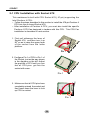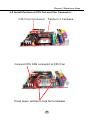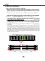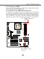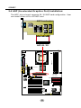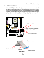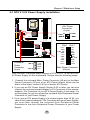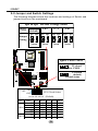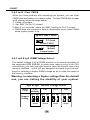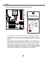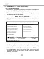
1
R
T h e
S o u l
O f
C o m p u t e r
T e c h n o l o g y
Mainboard
SL-85DRS2
User Manual V1.0
85DRS2
Product Model
Manual Revision
Release Date
: SL-85DRS2
: V1.0
: December 2001
NOTICE
This Users Guide & Technical Reference is to help system manufacturers and end-users set up and install the mainboard.Every effort has been made to ensure that the information in this manual is
accurate. Soltek Computer Inc. is not responsible for printing or
clerical errors. Information in this document is subject to change
without notice and does not represent a commitment on Soltek
Computer Inc.
No part of this manual may be reproduced, transmitted, translated
into any language in any form or by any means, electronic or
mechanical, including photocopying and recording, for any purpose
without the express written permission of Soltek Computer Inc.
Companies and products mentioned in this manual are for identification purpose only. Product names appearing in this manual may
or may not be registered trademarks or copyrights of their respective companies.
Soltek Computer Inc. provides this manual “as is “ without warranty
of any kind, either express or implied, including but not limited to the
implied warranties or conditions of merchantability or fitness for a
particular purpose. In no event shall Soltek Computer Inc. be liable
for any loss or profits, loss of business, loss of use or data, interruption of
business, or for indirect, special, incidental, or consequential damages of
any kind, even if Soltek Computer Inc. has been advised of the possibility
of such damages arising from any defect or error in this manual or product.
• Intel Pentium 4 is trademark of Intel Corporation.
• SiS, SiS 645 (A2), SiS 961 are trademarks of Silicon Integrated Systems
Corporation.
• AMI, AMIBIOS are trademarks of American Megatrends Inc.
• ITE, IT8705F are trademarks of Integrated Technology Express, Inc.
Copyright © 2001 Soltek Computer Inc. All Rights Reserved.
2
85DRS2
SOLTEK AROUND THE WORLD
SOLTEK COMPUTER INC.
Address
Telephone
Fax
E-mail
Web site
: 7F, No. 306-3, Ta-Tung Rd, Sec.1, Hsi-Chih, TaipeiHsien, Taiwan, R.O.C.
: 886-2-2642-9060
: 886-2-2642-9065
: [email protected]
: http://www.soltek.com.tw
SOUL TECHNOLOGY EUROPE B.V.
Address
Telephone
Fax
E-mail
Web site
: Hongkongstraat 55, 3047 BP Rotterdam. The Netherlands
: 31-10-2457492
: 31-10-2457493
: [email protected]
: http://www.soultech-europe.com
SOLTEK KOREA INC.
Address
Telephone
Fax
E-mail
: 1002, Chung Jin Bldg. 53-5 Wonhyo-Ro, 3-Ka,
Yongsan-Ku Seoul 140-113, Korea
: 82-2-32717400
: 82-2-32717405
: [email protected]
3
Contents
Contents
Chapter 1 Specification ............................................. 9
1-1 Main board Layout and Component Locations: .............. 10
1-2 Mainboard Specifications ..................................................... 11
1-2.1 CPU Socket ................................................................................... 11
1-2.2 System Chipsets ........................................................................... 11
1-2.3 Memory ......................................................................................... 11
1-2.4 AMI BIOS V2.01A ....................................................................... 11
1-2.5 Accelerated Graphics Port (AGP) Interface ........................... 11
1-2.6 Advanced System Power Management: .................................. 12
1-2.7 Multi-I/O Functions: ................................................................... 12
1-2.8 Expansion Slots ............................................................................ 12
1-2.9 Hardware Monitor on board ..................................................... 13
1-2.10 AC’97 Audio Codec on board ................................................. 13
1-2.11 Form Factor ................................................................................ 13
1-3 Mainboard Specification Table ........................................... 14
1-4 Chipset System Block Diagram ........................................... 15
Chapter 2 Hardware Setup ..................................... 17
2-1 CPU Installation with Socket 478 ....................................... 18
2-2 Install Pentium 4 CPU Fan and Fan Connector : ............ 19
2-3 Memory Installation ............................................................. 20
2-3.1 To Install DDR SDRAM Module for this Mainboard : ........ 20
2-3.2 To Remove a DIMM: ................................................................... 21
2-3.3 Indicator D7 for DIMM Socket Power On: ............................ 21
2-4 AGP (Accelerated Graphics Port) Installation: ............... 22
4
Contents
2-5 HDD Installation .................................................................... 23
2-6 Flopy Disk Drive (FDD) Installation .................................. 24
2-7 ATX V 2.03 Power Supply Installation .............................. 25
2-8 Jumper and Switch Settings ................................................ 26
2-8.1 Switch S3 for CPU Clock Select ................................................ 27
2-8.2 Jp10 Clear CMOS ...................................................................... 28
2-8.3 Jp2 & Jp3 DIMM Voltage Select: ............................................ 28
2-9 Other Connectors Configuration ........................................ 29
2-9.1 On Board FAN Connectors ........................................................ 29
2-9.2 WOL1 Wake On LAN Connector ............................................. 30
2-9.3 Connector Video-In ..................................................................... 30
2-9.4 CD-ROM Audio Connectors (CD_In1/CD_In2) .................... 31
2-9.5 Chassis Panel Connectors ......................................................... 31
2-9.6 Thermal Sensor Connectors RT1 and RT2 ............................. 32
2-9.7 Complex Header .......................................................................... 33
2-9.8 USB Ports and USB Header (Header USB 2) ......................... 35
2-9.9 PS/2 Mouse And PS/2 Keyboard ............................................... 35
2-10 IRQ Description ................................................................... 36
Chapter 3 Software Setup ....................................... 38
3-1 Open up Support CD: ........................................................... 39
3-2 Proceed to INF Driver Installation ..................................... 40
3-3 Proceed to AC’97 Audio Driver Installation ..................... 41
3-4 Proceed to Hardware Monitor Installation ..............................42
Chapter 4 BIOS Setup ............................................. 44
4-1 About BIOS Setup ................................................................. 45
4-2 To run BIOS Setup ................................................................ 45
4-3 About CMOS .......................................................................... 45
4-4 The POST ( Power On Self Test ) ....................................... 45
5
Contents
4-5 To upgrade BIOS ................................................................... 46
4-5.1 Before Upgrading BIOS ............................................................. 46
4-5.2 Upgrade Process ........................................................................... 46
4-6 BIOS SETUP --- CMOS Setup Utility ................................ 48
4-6.1 CMOS Setup Utility .................................................................... 48
4-6.2 Standard CMOS Setup ............................................................... 49
4-6.3 Advanced BIOS Features ........................................................... 52
4-6.4 Advanced Chipset Features ....................................................... 55
4-6.5 Power Management Setup ......................................................... 57
4-6.6 PNP / PCI Configuration ............................................................ 60
4-6.7 Integrated Peripherals ................................................................ 62
4-6.8 PC Health Status .......................................................................... 65
4-6.9 Frequency/Voltage Control ....................................................... 67
4-6.10 Set Supervisor / User Password ............................................. 69
4-6.11 Load Optimized Defaults ........................................................ 71
4-6.12 Save & Exit Setup ...................................................................... 71
4-6.13 Exit Without Saving .................................................................. 72
APPENDICES .......................................................... 74
Appendix-1 Identify Mainboard Model Number ................... 75
Appendix-2 Technical Terms ...................................................... 76
6
Contents
7
85DRS2
ITEM CHECKUP
Mainboard
Support CD
Bundled Bonus Pack CD
Bundled Bonus Pack Manual
Temperature Sensor Cable (Optional)
ATA66/100 IDE Cable
FDD Cable
User Manual
RS232 Cable
8
Chapter 1 Specification
Chapter 1 Specification
Introduction
This mainboard features an integration of the powerful processor Intel Pentium 4 and the single-chip North Bridge SiS 645 (A2 version).
The Intel P4 processor is a rapid execution engine providing 400MHz
quadpumped system bus to allow 3.2GB data transfer rates possible,
while North Bridge SiS 645 (A2) is an upgraded version of SiS 645 for
further advancing the performace of DRAM, 3D Graphics and the whole
system.
Together with South Bridge SiS 961, SiS 645 (A2) supports Intel P4
processor to execute the 400MHz FSB, the AGP 4X external bus, the
LPC Super I/O and the DDR SDRAM data transfer. This chapter is to
introduce to users every advanced function of this high performance
integration.
Topics included in this chapter are:
1-1 Mainboard Specifications
1-2 Mainboard Layout
1-3 Mainboard Specification Table
1-4 Chipset Diagram
9
85DRS2
1-1 Main board Layout and Component Locations:
D7
PS/2 Mouse
(on top)
DIMM
Indicator
FAN1
PS/2 K/B
(underside)
1
USB0
(on top)
mPGA478B
1
DDR 333
COM2
COM1
LPT1
USB1 (underside)
1
FAN2
1
Peripheral
3
1
+12V Power
SiS 645
(A2)
Main Power
Jp3
AGP 4X/2X
DIP
S3
Jp2
1 2 3 4 5
1
RT1
1
FAN3 1
PCI 1
DIMM 3
CD_IN1
ON
DIMM 2
Switch
DIMM 1
GAME/MIDI PORT
1
1
CD_IN2
1
IDE1
SiS
961
1
FDC
IR
PCI 5
PCI 6
IT8705F
LPC I/O
16 1
USB 2
1
10
RST
WOL1
HDD/LED
1
PWR SMI
RT2
30
PCI 4
Jp10
1
FAN4
FLASH BIOS
SUS LED
PCI 3
PWR LED
AC'97
Audio
1
IDE2
PCI 2
SPK
Video-In
Li
Battery
MIC
LINE LINE
IN
OUT
1
Chapter 1 Specification
1-2 Mainboard Specifications
1-2.1 CPU Socket
CPU Socket 478B on board, supporting Intel® Pentium 4 processors in
478-pin package for :
-- 400MHz System Bus;
-- Hyper pipelined technology;
-- Advanced dynamic execution;
-- Advanced transfer cache;
1-2.2 System Chipsets
North Bridge SiS 645 (A2) (advanced version of SiS 945) plus South
Bridge SiS 961 working with Intel Pentium 4 Processor for managing
and arbitrating operations between all system interfaces:
1-2.3 Memory
3 DDR DIMM 184-pin sockets on board for DDR333/266/200 SDRAMs,
supported by 2.5V default voltage :
• Supporting unbuffered SDRAM transfer rate 100/133/166MHz up to 3GB
DDR266/200 SDRAMs in 3 DIMMs or 2GB DDR333 in 2 DIMMs
• Supporting installation of mixed volumes yet same type of DDR SDRAM
modules
1-2.4 AMI BIOS V2.01A
•
•
•
•
Supporting Plug & Play V1.0
Flash Memory for easy upgrade
Supporting BIOS Writing Protection and Year 2000 compliant
Supporting BIOS Setup (Please see Chapter 4 BIOS Setup)
1-2.5 Accelerated Graphics Port (AGP) Interface
AGP Controller embedded, supporting:
• 1.5V/4X, 3.3V/2X power mode , AGP voltage selectable in BIOS Setup
• 2x/ 4x AD and SBA signalling, AGP pipelined split-transection longburst
transfers up to 1GB/sec.
• AGP v2.0 compliant
11
85DRS2
1-2.6 Advanced System Power Management:
• ACPI 1.0B compliant (Advanced Configuration and Power Interface)
• APM V1.2 compliant (Legacy power management)
• ACPI STR mode (Suspend To RAM) , POS (Power On Suspend) and
STD (Suspend to Disk)
• PS/2 Keyboard & Mouse power on
• Supporting Ring Power Up Control for Wake-on-Modem (external) and
Wake-on-LAN
• Real Time Clock (RTC) with date alarm, month alarm, and century field
• USB wake-up Function;
1-2.7 Multi-I/O Functions:
• PCI EIDE Controller, supporting:
-- 2x Ultra ATA100 / 66 / 33 IDE connectors supporting up to 4 IDE
devices
• Dedicated IR Functions:
-- Third serial port dedicated to IR function either through the two
complete serial ports or the third dedicated port Infrared-IrDA (HPSIR)
and ASK (Amplitude Shift Keyed) IR
• Multi-mode parallel Data transfer:
-- Standard mode, ECP and EPP support
• Floppy Disk connector:
-- One FDD connector with drive swap support
• Universal Serial Bus Transfer Mode:
-- USB V1.1 compliant;
-- 2 built-in USB connectors and one USB Header (USB2) which
requires an optional USB cable to provide 2 more optional USB ports
• PS/2 Keyboard
• PS/2 Mouse
• UARTs (Universal Asynchronous Receiver / Transmitter):
-- Two complete Serial Ports (COM1 & COM2) on board
1-2.8 Expansion Slots
• Six PCI bus Master slots
• One AGP 4x/2X slot
• Three DDR DIMM slots
12
Chapter 1 Specification
1-2.9 Hardware Monitor on board
Programmable hardware status to provide monitoring and alarm for flexible desktop management of hardware temperatures. Utility Software is
enclosed in Support CD to help display monitoring statuses of:
-- 6 voltages, 3 hardware temperatures, 2 Fan speeds
1-2.10 AC’97 Audio Codec on board
AC’97 Audio codec on board supported by AC97 Link on chip SiS 961
1-2.11 Form Factor
• ATX form factor, ATX power supply, version 2.03 compliant, supported by
one Main Power Connector, one +12V Power Connector and one Peripheral Power Connector
• Mainboard size: 305mm x 225mm
13
85DRS2
1-3 Mainboard Specification Table
Model
CPU
SL-85DRS2
Socket PGA 478B for Intel Pentium 4 CPU
Memory
Controller Hub
SiS 645 (A2 version)
I/O
Controller Hub
SiS 961
BIOS
AMI BIOS
I/O Chip
IT 8705F
Memory
Supporting DDR333/266/200 SDRAM up to 3GB
3 DIMM Slots
Onboard IDE
I/O Connectors
PCI slot
AGP Interface
Audio
2 x ATA 33/66/100 IDE ports
4 x USB ports, 1 x FDD port, 2 x COM ports,
1 x LPT port, 1 IrDA, 1 PS/2 Mouse, 1 PS/2 K/B
6 PCI Master Slots
AGP 4X Mode
AC'97 Audio Codec
Hardware¤
Monitoring
Power Supply
Yes
ATX 2.03 form factor
with one Main power Connector
one Peripheral Power Connector
one +12V Power Connector
BIOS writing
Protection
Yes
Keyboard power
on function &
USB wake up
Function
Yes
Remark
14
Chapter 1 Specification
1-4 Chipset System Block Diagram
Intel Pentium 4 Processor
System Bus (4x100MHz)
Bandwidth 3.2GB/s
with 2X address/4X data
DDR
Memory
Interface
AGP 4x
(1.5V)
AGP Graphics
SiS 645 (A2)
-System Bus
-Memory Controller
DDR333/266/
200 SDRAM
System
Memory
-AGP Controller
Bi-directional 15-bit data bus,
at 266MHz operating frequency,
533MH/s bandwidth
HDD
CD-ROM
PCI Slots
PCI Bus
ATA100/66/33
SiS 961
USB Ports
USB Bus
IR
FD
Mouse
Keyboard
Serial Ports
Printer Port
Game/MIDI
I/O Control Hub
AC'97 2.1
Audio Codec
LPC I/O
Chip IT8705F
BIOS
Intel Pentium 4 + SiS 645 (A2) + SiS 961 Diagram
15
85DRS2
MEMO
MEMO
16
Chapter 2 Hardware Setup
Chapter 2 Hardware Setup
To Get things ready for Hardware setup !
1. We recommend to install your CPU before any other components.
For detailed installation instructions of processor, you can also refer
to the pamphlet enclosed in your CPU package.
2. Installing a cooling fan with a good heatsink is a must for proper heat
dissipation for your CPU. Get ready an appropriate fan with heatsink
for proper installation. Improper fan and installation will damage your
CPU.
3. In case CPU Vcore, CPU clock or Frequency Ratio is adjustable on
board, please follow the instructions described in the User manual
for proper setup. Incorrect setting will cause damage to your CPU.
The following topics are included in this chapter:
2-1 Pentium 4 CPU Installation
2-2 Pentium 4 CPU Fan Installation
2-3 Memory Installation
2-4 HDD Installation
2-5 FDD Installation
2-6 AGP (Accelerated Graphic Port) Installation
2-7 ATX 2.03 Power Supply Installation
2-8 Jumper Settings for Devices on board
2-9 Other Connectors Configuration
2-10 IRQ Description
17
85DRS2
2-1 CPU Installation with Socket 478
This mainboard is built with CPU Socket 478 ( 47-pin) supporting the
Intel Pentium 4 CPU:
• Follow the steps described in this section to install the 478-pin Pentium 4
CPU into the on board Socket 478.
• After installation of Pentium 4 CPU, you must also install the specific
Pentium 4 CPU fan designed in tandem with this CPU. This CPU Fan
installation is described in next section.
m
PG
A
47
8B
1. First pull sideways the lever of
Socket 478, and then turn it up
900 so as to raise the upper layer
of the socket from the lower
platform.
Pin 1
Inte
m
PG
A4
78
B
l Pe
ntiu
m4
2. Configure Pin 1 of CPU to Pin 1 of
the Socket, just as the way shown
in the diagram on the left. Adjust
the position of CPU until you can
feel all CPU pins get into the
socket with ease.
Pin 1
Intel Pentium 4
mPGA478B
3. Make sure that all CPU pins have
completely entered the socket and
then lower down the lever to lock
up CPU to socket.
Pin 1
18
Chapter 2 Hardware Setup
2-2 Install Pentium 4 CPU Fan and Fan Connector :
CPU Fan Connector
Pentium 4 Fanbase
Connect CPU FAN connector to CPU Fan
Press down latches to lock fan to fanbase
19
85DRS2
2-3 Memory Installation
How to tackle with the memory Modules:
• Make sure to unplug your power supply before adding or removing memory
module. Failure to do so may cause severe damage to both your main
board and the memory module.
• Pay attention to the orientation of the DIMM slots. Forcing a DIMM in a
socket improperly will damage the memory module and socket.
• Make sure you have the right type of memory module for your mainboard.
2-3.1 To Install DDR SDRAM Module for this Mainboard :
1. This mainboard only supports unbuffered DDR SDRAM. Do not insert
other type of DDR SDRAM therein.
2. For DDR333, this mainboard can support up to 2GB memory in two
DIMMs.That is, you can only use 1 or 2 DDR333 SDRAM modules.
3. For DDR266/200, this mainboard can support up to 3 GB memory in
3 DIMMs.
4. DDR DIMM socket has 184 pins and one notch. Insert a DDR SDRAM
vertically into the 184-pin socket with its notch matching the one in
the socket. Press the Module down in a gradual way until it surely
reaches the bottom and clicks straight up the two latches on the left
and right side of the socket. If any one of the latches has not turned
up completely, you should unplug the module and press it down the
socket a bit more firmly.
184-Pin DIMM Notch Key Definitions (2.5V)
DRAM Key Position
Voltage Key Position
2.5V
Module Latch
20
Chapter 2 Hardware Setup
2-3.2 To Remove a DIMM:
Press down the holding latches on both sides of socket and the module
will be released from the DIMM socket.
2-3.3 Indicator D7 for DIMM Socket Power On:
An indicator D7 is designed on board. Whenever system is started or
is in STR status (Suspend to RAM), all the DIMM sockets on board will
also get powered on with the set voltage, resulting in D7 lighting up.
This indicator D7 is to warn users that, whenever DIMM socket is
powered, no memory module should be removed from or added into it.
DIMM Power On
Indicator
D7
D7
PS/2 Mouse
(on top)
DIMM
Indicator
FAN1
PS/2 K/B
(underside)
1
USB0
(on top)
mPGA478B
1
DDR 333
COM2
COM1
LPT1
USB1 (underside)
1
FAN2
1
Peripheral
3
1
+12V Power
SiS 645
(A2)
Main Power
Jp3
AGP 4X/2X
S3
Jp2
1
RT1
1
FAN3 1
PCI 1
DIMM 3
DIP
1 2 3 4 5
DIMM 2
ON
DIMM 1
Switch
CD_IN1
1
1
CD_IN2
1
IDE1
SiS
961
1
FDC
PCI 5
PCI 6
IT8705F
LPC I/O
RST
IR
WOL1
HDD/LED
1
PWR SMI
RT2
30
PCI 4
SUS LED
PCI 3
PWR LED
AC'97
Audio
1
IDE2
PCI 2
SPK
Video-In
Li
Battery
LINE LINE
IN
OUT
MIC
GAME/MIDI PORT
1
16 1
USB 2
1
Jp10
1
FAN4
FLASH BIOS
DDR DIMM Sockets
(184-pin)
21
85DRS2
2-4 AGP (Accelerated Graphics Port) Installation:
The AGP slot on board supports 4X / 2X AGP card configuration. User
can install either a 4X or 2X AGP card.
AGP Accelerator
AGP 4X / 2X
D7
PS/2 Mouse
(on top)
DIMM
Indicator
FAN1
PS/2 K/B
(underside)
1
USB0
(on top)
mPGA478B
1
DDR 333
COM2
COM1
LPT1
USB1 (underside)
1
FAN2
1
Peripheral
3
1
+12V Power
SiS 645
(A2)
Main Power
Jp3
AGP 4X/2X
S3
Jp2
1 2 3 4 5
1
RT1
1
FAN3 1
PCI 1
DIMM 3
DIP
DIMM 2
CD_IN1
ON
DIMM 1
Switch
1
1
CD_IN2
1
IDE1
SiS
961
1
FDC
PCI 6
IT8705F
LPC I/O
16 1
USB 2
1
22
RST
IR
PCI 5
HDD/LED
WOL1
PWR SMI
RT2
1
30
PCI 4
Jp10
1
FAN4
FLASH BIOS
SUS LED
PCI 3
PWR LED
AC'97
Audio
1
IDE2
PCI 2
SPK
Video-In
Li
Battery
LINE LINE
IN
OUT
MIC
GAME/MIDI PORT
1
Chapter 2 Hardware Setup
2-5 HDD Installation
To install HDD (Hard Disk Drive), you may connect the connector of
IDE cable to the primary (IDE1) or secondary (IDE2) connector on board,
and then connect the gray connector to your slave device and the black
connector to your master device. If you install two hard disks, you must
configure the second drive to Slave mode by setting its jumpers correctly.
Please refer to your hard disk documentation for the jumper settings.
D7
PS/2 Mouse
(on top)
DIMM
Indicator
FAN1
PS/2 K/B
(underside)
1
USB0
(on top)
mPGA478B
1
DDR 333
COM2
COM1
LPT1
USB1 (underside)
1
FAN2
IDE2
1
Peripheral
3
1
+12V Power
(A2)
Main Power
Jp3
AGP 4X/2X
DIP
S3
Jp2
1 2 3 4 5
1
RT1
1
FAN3 1
PCI 1
1
DIMM 3
ON
DIMM 2
Switch
CD_IN1
1
CD_IN2
1
IDE1
SiS
961
1
FDC
30
PCI 4
PWR SMI
RT2
PCI 5
Pin 1 (to Red Line)
RST
IT8705F
LPC I/O
HDD/LED
PCI 6
Li
Battery
IR
WOL1
Hard Disk Drive Connector:
Orient the red line on the IDE
ribbon cable to Pin1.
SUS LED
PCI 3
PWR LED
AC'97
Audio
1
IDE2
PCI 2
SPK
Video-In
1
IDE1
SiS 645
DIMM 1
LINE LINE
IN
OUT
MIC
GAME/MIDI PORT
1
16 1
USB 2
1
Jp10
1
FAN4
FLASH BIOS
Gray connector
Black connector
red line
Blue connector
IDE Cable
23
85DRS2
2-6 Flopy Disk Drive (FDD) Installation
To install FDD (Floppy Disk Drive), you should connect the end of the
cable with single connector to the board , and connect the other end
with two connectors to the floppy drives.
D7
PS/2 Mouse
(on top)
DIMM
Indicator
FAN1
PS/2 K/B
(underside)
1
USB0
(on top)
mPGA478B
1
FAN2
1
Floppy Disk Drive
Connector:
Orient the red line on
the floppy ribbon cable
to Pin1.
DDR 333
COM2
COM1
LPT1
USB1 (underside)
1
Peripheral
3
1
+12V Power
SiS 645
(A2)
Main Power
Jp3
AGP 4X/2X
1
RT1
1
FAN3 1
Pin 1 (to Red Line)
Jp2
PCI 1
1
DIMM 3
S3
1 2 3 4 5
DIMM 2
DIP
DIMM 1
Switch
CD_IN1
ON
1
CD_IN2
1
IDE2
1
IDE1
SiS
961
1
FDC
30
PCI 4
PCI 5
IR
WOL1
PWR SMI
RT2
1
FDC
RST
HDD/LED
PCI 6
IT8705F
LPC I/O
SUS LED
PCI 3
PWR LED
PCI 2
SPK
Video-In
AC'97
Audio
Li
Battery
LINE LINE
IN
OUT
MIC
GAME/MIDI PORT
1
16 1
USB 2
1
Jp10
1
FAN4
FLASH BIOS
To 2nd Floppy Drive
red line
To 1st Floppy Drive
FDD Cable
24
To mainboard
Chapter 2 Hardware Setup
2-7 ATX V 2.03 Power Supply Installation
D7
PS/2 Mouse
(on top)
DIMM
Indicator
FAN1
PS/2 K/B
(underside)
1
USB0
(on top)
mPGA478B
1
FAN2
1
+12V Power
Connector
(4-pin)
DDR 333
COM2
COM1
LPT1
USB1 (underside)
1
Peripheral
3
1
+12V Power
SiS 645
(A2)
Main Power
Jp3
DIP
S3
1 2 3 4 5
1
RT1
1
FAN3 1
PCI 1
DIMM 3
ON
Jp2
DIMM 2
Switch
CD_IN1
AGP 4X/2X
DIMM 1
LINE LINE
IN
OUT
MIC
GAME/MIDI PORT
1
1
1
+12V 4
3 +12V
GND 2
1 GND
CD_IN2
1
IDE1
SiS
961
1
FDC
30
PCI 4
PCI 5
16 1
USB 2
1
Peripheral
Power
Connector
(4-pin)
Pin 1
Pin 4
RST
IT8705F
LPC I/O
HDD/LED
PCI 6
Li
Battery
IR
WOL1
PWR SMI
RT2
1
Jp10
1
FAN4
SUS LED
PCI 3
PWR LED
AC'97
Audio
1
IDE2
PCI 2
FLASH BIOS
+12V
GND
GND
+5V
SPK
Video-In
PIN1
+12V
5SB
PWR_OK
GND
+5V
GND
+5V
GND
+3.3V
+3.3V
Pin11
+5V
+5V
-5V
GND
GND
GND
PS_ON#
GND
-12V
+3.3V
Main Power Connector
(20-pin)
Intel Pentium 4 requires power support of ATX V2.03. To set up ATX2.
03 Power Supply on this mainboard, Please take the following steps:
1. Connect the on-board Main Power Connector (20-pin) to the Main
Power Connector (20-pin) of an ATX Power Supply which can be
either of the latest version 2.03 or of earlier ATX format.
2. If you use an ATX Power Supply Version 2.03 or later, you can now
connect the on-board square-shaped +12V Connector to the squareshaped +12V Connector of your ATX Power Supply. In this case, it is
not necessary for you to connect the on-board 4-pin Peripheral Power
Connector to your Power Supply.
3. If you use an ATX power Supply of a version earlier than V2.03, you
cannot find a square-shaped +12V Connector with your Power Supply;
you must then connect the on-board 4-pin Peripheral Power
Connector to the 4-pin Peripheral Power Connector of your Power
Supply.
25
85DRS2
2-8 Jumper and Switch Settings
The following diagrams show the locations and settings of Switch and
jumper blocks on the mainboard.
Jp2 & Jp3 DIMM Voltage Select
DIMM
2.5VJ
2.6VJ
2.7VJ
2.8VJ
Voltage
(default)
Jp2J Jp3J Jp2J Jp3J
Jumper
Setting 1J
1J
1J
1-2J 1-2J
closedJ
1J
Jp2J Jp3J
1J
1J
Jp2J Jp3J
1J
1-2J 2-3 J 2-3 J 1-2J
closedJ
closedJ
1J
2-3 J 2-3 J
closedJ
D7
PS/2 Mouse
(on top)
DIMM
Indicator
FAN1
PS/2 K/B
(underside)
1
USB0
(on top)
mPGA478B
1
DDR 333
COM2
COM1
LPT1
USB1 (underside)
1
FAN2
Jp10 Clear CMOS
1
Peripheral
3
1
+12V Power
SiS 645
1 2-3 closed
(A2)
Main Power
Jp3
S3
Jp2
1 2 3 4 5
CD_IN1
1
RT1
1
FAN3 1
PCI 1
DIMM 3
DIP
DIMM 2
ON
DIMM 1
Switch
AGP 4X/2X
1
To clear CMOS
1
CD_IN2
IDE2
1
FDC
30
PCI 4
PCI 5
IR
WOL1
PCI 6
16 1
USB 2
1
S3
On
RST
IT8705F
LPC I/O
HDD/LED
1
PWR SMI
RT2
SUS LED
SiS
961
1
1
IDE1
PCI 3
PWR LED
PCI 2
1-2 closed
(default)
Normal status
1
SPK
Video-In
AC'97
Audio
Li
Battery
LINE LINE
IN
OUT
MIC
GAME/MIDI PORT
1
Jp10
1
FAN4
FLASH BIOS
DIP
ON
CPU Clock Select
Off
1 2 34 5
On On Off Off Off (Default)
DDR
type
DDR266
DDR333
CPU Clock
S3-1
(MHz)
default 100 on
105
108
112
133
100
133
off
off
off
off
on
on
S3-2 S3-3 S3-4 S3-5
on
off
off
off
off
off
off
on
on
on
off
off
off
off
on
on
on
on
on
off
off
off
off
on
on
on
off
on
26
Chapter 2 Hardware Setup
How to tackle with Jumpers:
• Do not remove the jumper when power is on. Always make sure
the power is off before changing any jumper settings. Otherwise,
mainboard could be damaged.
• In the Jumper setting diagram, all jumper pins covered with black
marks stand for closed pins by jumper caps.
2-8.1 Switch S3 for CPU Clock Select
1. This mainboard is shipped to users with a 5-DIP Switch on board, by
which user can select a CPU clock to match with the Pentium 4
processor installed on board. Yet users are not recommended to
take Switch S3 as a foolproof tool for overclocking. Instead, it is
saver and more advisable to select the CPU clock as near as possible
to the one marked on the selected CPU.
2. An Advice from our Engineering Team:
CPU Overclocking should always take the on-board components into
account. If you are using DDR266 SDRAM on this mainboard, you must
not set the switch S3 to the DDR333 settings; otherwise you risk system
damage.
S3
On
DIP
ON
CPU Clock Select
Off
1 2 34 5
On On Off Off Off (Default)
DDR
type
DDR266
DDR333
CPU Clock
S3-1
(MHz)
default 100 on
105
108
112
133
100
133
off
off
off
off
on
on
S3-2 S3-3 S3-4 S3-5
on
off
off
off
off
off
off
on
on
on
off
off
off
off
on
on
on
on
on
off
off
off
off
on
on
on
off
on
27
85DRS2
2-8.2 Jp10 Clear CMOS
When you have problem with rebooting you system, you can clear
CMOS data and restore it to default value. To clear CMOS with Jumper
Jp10, please follow the steps below:
1. Power off system;
2. Set JBAT1 to Pin 2-3 closed.
3. After 2 or 3 seconds, return the JBAT1 setting to Pin1-2 closed.
4. CMOS data are restored to default. Remember never clear CMOS
when system power is on.
Jp10 Clear CMOS
1 2-3 closed
To clear CMOS
1-2 closed
(default)
Normal status
1
2-8.3 Jp2 & Jp3 DIMM Voltage Select:
The default voltage 2.5V at DIMM sockets is for normal operation of
the supported DDR SDRAM. In some case, when you try to do CPU
overclocking, you then may also need to raise the transfer rate of the
memory interface. Jp2 & Jp3 are designed on board to provide settings for selecting a higher DIMM voltage so as to raise the speed of
the memory interface.
Warning: In selecting a higher voltage than the default
one, you are risking the stability of your system.
Jp2 & Jp3 DIMM Voltage Select
DIMM
2.5VJ
2.6VJ
2.7VJ
2.8VJ
Voltage
(default)
Jp2J Jp3J Jp2J Jp3J
Jumper
Setting 1J
1J
1-2J 1-2J
closedJ
1J
1J
Jp2J Jp3J
1J
1J
1-2J 2-3 J 2-3 J 1-2J
closedJ
closedJ
28
Jp2J Jp3J
1J
1J
2-3 J 2-3 J
closedJ
Chapter 2 Hardware Setup
2-9 Other Connectors Configuration
This section lists out all connectors configurations for users’ reference.
2-9.1 On Board FAN Connectors
D7
PS/2 Mouse
(on top)
DIMM
Indicator
FAN1
PS/2 K/B
(underside)
1
USB0
(on top)
mPGA478B
1
DDR 333
COM2
COM1
LPT1
USB1 (underside)
1
FAN2
CPU FAN Connector
FAN1, yellow, sensor
1
Peripheral
1
+12V Power
SiS 645
(A2)
Main Power
Jp3
AGP 4X/2X
DIP
S3
Jp2
1 2 3 4 5
1
RT1
1
FAN3 1
PCI 1
DIMM 3
ON
DIMM 2
Switch
CD_IN1
DIMM 1
LINE LINE
IN
OUT
MIC
GAME/MIDI PORT
1
3
GND
+12V
SENSOR
1
1
Power FAN Connector
FAN2, no sensor
CD_IN2
1
IDE1
PCI 3
SiS
961
1
FDC
PCI 5
RST
System FAN Connector
FAN4, no sensor
SPK
IT8705F
LPC I/O
HDD/LED
PCI 6
Li
Battery
IR
WOL1
PWR SMI
RT2
1
30
PCI 4
AGP FAN Connector
FAN3, yellow, sensor
SUS LED
AC'97
Audio
1
IDE2
PCI 2
PWR LED
Video-In
16 1
USB 2
1
Jp10
1
FAN4
FLASH BIOS
These fan connectors support CPU/Power/AGP/System cooling fan
with +12V. When connecting the wire to FAN connectors, users should
make sure that the red wire is for the positive current and should be
connected to pin +12V, and the black wire is Ground and should be
connected to pin GND. If your mainboard has Hardware Monitor chipset
on board, you must use a specially designed fan with speed sensor to
take advantage of the monitoring function.
For fans with speed sensors, each rotation of the fan blades will send
out 2 electric pulses, by which System Hardware Monitor will work out
the fan rotation speed by counting the pulses.
NOTE : 2 “Yellow” fan connectors are used on this series to mark that
they support fan speed sensor function. The other two white fan connectors
do not support sensor function.
29
85DRS2
2-9.2 WOL1 Wake On LAN Connector
1. This connector connects to a LAN card with a Wake On Ring output.
The connector powers up the system when it receives a wake-up
packet or signal through the LAN card.
2. This feature requires that Ring Power Up Control feature is enabled
in the BIOS setting “Power Management Setup” and that your system
must be on ATX power supply with at least 720mA / +5V standby
power.
D7
PS/2 Mouse
(on top)
DIMM
Indicator
FAN1
PS/2 K/B
(underside)
1
USB0
(on top)
GND
+5V
Standby
Ring
mPGA478B
1
DDR 333
COM2
COM1
LPT1
USB1 (underside)
1
FAN2
1
3
1
+12V Power
SiS 645
(A2)
Main Power
Jp3
S3
Jp2
1 2 3 4 5
1
RT1
1
PCI 1
FAN3 1
1
DIMM 3
ON
DIMM 2
Switch
CD_IN1
AGP 4X/2X
DIP
DIMM 1
LINE LINE
IN
OUT
MIC
GAME/MIDI PORT
Peripheral
1
1
Wake On LAN Connector:
CD_IN2
1
IDE1
SiS
961
30
PCI 4
PWR SMI
RT2
PCI 5
WOL1
Li
Battery
IR
1
WOL1 LAN card to WOL1
RST
IT8705F
LPC I/O
HDD/LED
PCI 6
Connect the Wake
On LAN signal from
1
FDC
SUS LED
PCI 3
PWR LED
AC'97
Audio
1
IDE2
PCI 2
SPK
Video-In
16 1
USB 2
1
Jp10
1
FAN4
FLASH BIOS
2-9.3 Connector Video-In
This connector connects to the Video Tuner Card and acts as Audio
Input connector.
D7
PS/2 Mouse
(on top)
DIMM
Indicator
FAN1
PS/2 K/B
(underside)
1
USB0
(on top)
Connector Video-In
mPGA478B
1
DDR 333
COM2
COM1
LPT1
USB1 (underside)
1
FAN2
1
1
Peripheral
3
1
+12V Power
Pin 1 R-Channel
SiS 645
(A2)
Main Power
Jp3
AGP 4X/2X
1 2 3 4 5
1
RT1
1
FAN3 1
PCI 1
DIMM 3
S3
Pin 2 GND
Jp2
DIMM 2
DIP
DIMM 1
Switch
CD_IN1
ON
1
1
Pin 3 GND
CD_IN2
1
IDE2
SiS
961
1
FDC
PCI 6
IT8705F
LPC I/O
RST
IR
PCI 5
HDD/LED
WOL1
PWR SMI
RT2
1
30
PCI 4
SUS LED
PCI 3
Pin 4 L-Channel
1
IDE1
PWR LED
PCI 2
SPK
Video-In
AC'97
Audio
Li
Battery
LINE LINE
IN
OUT
MIC
GAME/MIDI PORT
1
16 1
USB 2
1
Jp10
1
FAN4
FLASH BIOS
30
Chapter 2 Hardware Setup
2-9.4 CD-ROM Audio Connectors (CD_In1/CD_In2)
Both CD-In1 and CD-In2 are audio connectors connecting CD-ROM
audio to mainboard. Only take notice that Connector CD-In1 is of narrower pin pitch.
D7
PS/2 Mouse
(on top)
DIMM
Indicator
FAN1
PS/2 K/B
(underside)
1
USB0
(on top)
CD-ROM Audio Pin Assignment
mPGA478B
1
1
FAN2
CD_IN1
1
1
Peripheral
1
+12V Power
Pin 2
Pin 3
Pin 4
GND
Left
Channel
GND
Right
Channel
GND
GND
Right
Channel
Left
CD_IN2 Channel
SiS 645
(A2)
Main Power
Jp3
AGP 4X/2X
DIP
S3
Jp2
1 2 3 4 5
1
RT1
1
PCI 1
FAN3 1
DIMM 3
ON
DIMM 2
Switch
CD_IN1
DIMM 1
LINE LINE
IN
OUT
MIC
GAME/MIDI PORT
1
3
Pin 1
1
DDR 333
COM2
COM1
LPT1
USB1 (underside)
1
1
CD_IN2
AC'97
Audio
1
IDE2
PCI 2
1
IDE1
PCI 3
SiS
961
1
FDC
30
PCI 4
PWR SMI
RT2
PWR LED
PCI 5
WOL1
RST
IT8705F
LPC I/O
SPK
HDD/LED
PCI 6
Li
Battery
IR
1
SUS LED
Video-In
16 1
USB 2
1
Jp10
1
FAN4
FLASH BIOS
2-9.5 Chassis Panel Connectors
A
B
C
D
E
F
A.
B.
E.
F.
C.
D.
G.
: PS/2 MOUSE PORT
: USB 0 PORT
: LPT1 PORT
: GAME/MIDI PORT
: PS/2 KEYBOARD PORT
: USB 1 PORT
H.
G
H
I
J
K
31
I.
J.
K.
: COM1 PORT
: COM2 PORT
: LINE/SPEAKER OUT
: LINE IN
: MICROPHONE INPUT
85DRS2
2-9.6 Thermal Sensor Connectors RT1 and RT2
D7
PS/2 Mouse
(on top)
DIMM
Indicator
FAN1
PS/2 K/B
(underside)
1
USB0
(on top)
mPGA478B
1
FAN2
1
RT1
DDR 333
COM2
COM1
LPT1
USB1 (underside)
RT1 mounted with
blue Thermal Resistor
1
Peripheral
3
1
+12V Power
SiS 645
(A2)
Main Power
Jp3
AGP 4X/2X
DIP
S3
Jp2
1 2 3 4 5
1
RT1
1
FAN3 1
PCI 1
DIMM 3
ON
DIMM 2
Switch
CD_IN1
DIMM 1
LINE LINE
IN
OUT
MIC
GAME/MIDI PORT
1
1
1
Thermal Cable
CD_IN2
PCI 2
1
IDE1
PCI 3
SiS
961
1
FDC
PCI 5
RST
To Devices
SPK
IT8705F
LPC I/O
HDD/LED
PCI 6
Li
Battery
IR
WOL1
PWR SMI
RT2
1
30
PCI 4
SUS LED
AC'97
Audio
1
IDE2
PWR LED
Video-In
16 1
USB 2
1
Jp10
1
FAN4
FLASH BIOS
To RT2
RT2
1. Connector RT1: A blue thermal resistor is already soldered to
connector RT1 so as to sense the temperature round the mainboad.
What RT1 does is to transmit the thermal signal to BIOS or Hardware
Monitor.
2. Connector RT2: A thermal cable is needed to connect RT2 to onboard devices such as HDD, Graphics card etc., so as to detect the
temperature generated therein. Please connect the end (a) of the
thermal cable to mainboard RT2 header, and tape another end (b) of
thermal cable on to the device which you want to monitor. After you
have finished the thermal cable installation, you will see the detected
temperature in BIOS setup or Hardware monitor utility.
32
Chapter 2 Hardware Setup
2-9.7 Complex Header
This complex Header consists of 9 connectors providing various
supports:
D7
PS/2 Mouse
(on top)
DIMM
Indicator
FAN1
PS/2 K/B
(underside)
1
USB0
(on top)
mPGA478B
1
DDR 333
COM2
COM1
LPT1
USB1 (underside)
1
FAN2
1
Peripheral
3
+12V Power
1
SiS 645
(A2)
Main Power
Jp3
S3
Jp2
1 2 3 4 5
1
RT1
1
FAN3 1
PCI 1
1
DIMM 3
CD_IN1
AGP 4X/2X
DIP
ON
DIMM 2
Switch
DIMM 1
LINE LINE
IN
OUT
MIC
GAME/MIDI PORT
1
1
CD_IN2
1
IDE1
SiS
961
1
FDC
30
PCI 4
PWR SMI
RT2
PCI 5
WOL1
16 1
USB 2
1
1 SMI
2 Power Switch
GND
Jp10
1
SUSPEND LED SIGNAL
(-)
GND
NO CONNECTION
Vcc
GND
INFRARED TRANSMIT SIGNAL
GND
1st HDD LED
Suspend LED 5
ATX POWER SWITCH
INFRARED TRANSMIT SIGNAL
2nd HDD LED
FLASH BIOS
Vcc
Vcc
4
FAN4
GND
SMI SIGNAL
NO CONNECTION
3 Infrared(IR)
RST
IT8705F
LPC I/O
HDD/LED
PCI 6
Li
Battery
IR
1
SUS LED
PCI 3
PWR LED
AC'97
Audio
1
IDE2
PCI 2
SPK
Video-In
RESET SIGNAL
SPEAKER SIGNAL¤
(+)
(-)
HDD LED SIGNAL (-)
Logic High (+)
Logic High
HDD LED SIGNAL
Power LED 6
(+)
Reset Switch 7
GND¤
NO CONNECTION¤
Vcc¤
33
Speaker 8
85DRS2
(1) SMI Connector (System Management Interrupt):
Connection: Connected to the case-mounted Suspend Switch.
Function: Manually selecting system into the Suspend Mode or
“Green Mode”.
(2) Power Switch Connector:
Connection: Connected to a momentary button or switch.
Function: Manually switching the system between “On” and “Soft
Off”. Pressing the momentary button for more than 4 seconds
will also turn the system off.
(3) IR Connector (Infrared Connector):
Connection: Connected to Connector IR on board.
Function: Supporting wireless transmitting and receiving module on board.
(4) 1st HDD LED Connector / 2nd HDD LED Connector:
Connection: Connected to HDD LED.
Function: To supply power to HDD LED.
(5) Suspend LED Connector:
Connection: Connected to Suspend indicator.
Function: To supply power to “Suspend indicator”.
(6) Power LED Connector:
Connection: Connected to System Power LED.
Function: To supply power to “System Power LED”.
(7) Reset Switch Connector:
Connection: Connected to the case-mounted “Reset Switch”.
Function: To supply power to “Reset Switch” and support system reboot function.
(8) Speaker Connector:
Connection: Connected to the case-mounted Speaker.
Function: To supply power to the case-mounted Speaker.
34
Chapter 2 Hardware Setup
2-9.8 USB Ports and USB Header (Header USB 2)
This series of mainboards provides two USB ports USB0 and USB1
on board supporting various USB devices. In addition, one USB header
is added on board to provide two additional USB ports by using an additional USB Cable. User can order the additional USB cable from your
mainboard dealer or vender.
When plugging the USB cable into Header USB2, user must make
sure the red wire is connected to Pin 1.
USB Ports USB 0 & 1
USB Cable (Optional)
D7
PS/2 Mouse
(on top)
DIMM
Indicator
FAN1
PS/2 K/B
(underside)
1
USB0
(on top)
mPGA478B
1
USB Port
DDR 333
COM2
COM1
LPT1
USB1 (underside)
1
FAN2
USB2
1
Peripheral
3
1
+12V Power
SiS 645
(A2)
USB I
P4D - GND
Main Power
Jp3
AGP 4X/2X
DIP
S3
Jp2
1 2 3 4 5
1
RT1
1
FAN3 1
PCI 1
DIMM 3
CD_IN1
ON
DIMM 2
Switch
DIMM 1
LINE LINE
IN
OUT
MIC
GAME/MIDI PORT
1
1
1
SiS
961
WOL1
30
PCI 5
+5V
10
16 1
USB 2
1
Jp10
1
FAN4
USBI Void
P2D +
¤
RST
IT8705F
LPC I/O
HDD/LED
PCI 6
Li
Battery
IR
1
PWR SMI
RT2
1
1
1
FDC
PCI 4
USBI
P4D + N/C
10
1
IDE1
PCI 3
SUS LED
PCI 2
PWR LED
AC'97
Audio
1
IDE2
SPK
Video-In
+5V
Red wire
CD_IN2
FLASH BIOS
1
10
USB I GND
P2D -
USB2 Header
Pin Assignment
Header USB 2
2-9.9 PS/2 Mouse And PS/2 Keyboard
PIN 6 : Void
PIN 5 : Mouse Clock
PIN 4 : Vcc
PIN 3 : GND
PIN 2 : Void
PIN 1 : Mouse Data
PIN 6 : Void
PIN 5 : Keyboard Clock
PIN 4 : Vcc
PIN 3 : GND
PIN 2 : Void
PIN 1 : Keyboard Data
PS/2 MOUSE
PS/2 KEYBOARD
35
85DRS2
2-10 IRQ Description
IRQII
IRQI 0I
Function DescriptionI
System TimerII
Priority
1
IRQI 1I
Keyboard ControllerI
2
IRQI 2I
Programmable InterruptI
N/A
IRQI 3I
Serial Port (COM 2)I
11
IRQI 4I
Serial Port (COM 1)I
12
IRQI 5I
FreeI
13
IRQI 6I
Floppy Disk ControllerI
14
IRQI 7I
Parallel Port (LPT1)I
15
IRQI 8I
Real Time Clock (RTC)I
3
IRQI 9I
FreeI
4
IRQI 10I
FreeI
5
IRQI 11I
FreeI
6
IRQI 12I
PS/2 Mouse PortI
7
IRQI 13I
CoprocessorI
8
IRQI 14I
Primary IDE ChannelI
9
IRQI 15I
Secondary IDE ChannelI
10
• Both ISA and PCI expansion cards may require IRQs. System IRQs are
available to cards installed in the ISA expansion bus first, then any remaining IRQs are available to PCI cards. Currently, there are two types of
ISA cards.
• The original ISA expansion card design, now referred to as “Legacy” ISA
card, requires you to configure the card’s jumpers manually and then install it in any available slot on the ISA bus. To see a map of your used and
free IRQs in Windows 98, the Control Panel in My Computer, contains a
System icon, which gives you a Device Manager tab. Double-Clicking
on a specific hardware device gives you a Resources tab which shows
the Interrupt number and address. Double-Clicking Computers to see all
the interrupts and addresses for your system. Make sure that each ISA
device should be assigned to one IRQ respectively. If ISA device share
IRQ with any other device, your computer will easily get into trouble.
36
Chapter 2 Hardware Setup
MEMO
MEMO
37
85DRS2
Chapter 3 Software Setup
Drivers, Utilities and Software Installation
Support CD:
This mainboard is shipped with a Support CD which contains those
necessary driver files, Application Softwares and some helpful utilities.
It is a user-friendly, auto-run CD which will open itself up in a CD-ROM
automatically.
Contents of Support CD:
User will be able to find in the Support CD the following drivers and
utilities supported by SiS 645 Chipset:
1. INF;
2. AC’97 Audio Drivers;
3. Hardware Monitor Utility;
This chapter is devoted to describing the installations of all these
essential drivers and utilities on Windows 9X, Windows ME Windows
NT Windows 2000 and Windows XP. The driver installation procedures for all these operating sistems are programed into an auto-run
mode. What users have to do is read and follow the pop-up instructions.
We herein take the installation on Windows 98 as the general illustration.
The priority of driver installation should also be noted. Users are recommended to take the following installation order:
3-1 Open Support CD and choose your drivers
3-2 Install INF Driver
3-3 AC’97 Audio Driver Installation
3-4 Hardware Monitor Utility Installation
38
Chapter 3 Software Installation
3-1 Open up Support CD:
1. Please put the Support CD enclosed in your mainboard package into
the CD-ROM drive. In a few seconds, the Main Menu will automatically appear, displaying the contents to be installed for this mainboard:
Install INF
Install AC’97 Audio Driver
Install Hardware Monitor Utility
Install Acrobat Reader
Browse CD-ROM
Exit
2. In case your system does not open the Support CD automatically,
pleaseclick to the following path to enter the Main Installation Menu:
D:\ Autorun.exe (assuming that your CD-ROM Drive is Drive D)
3. Users are recommended to install all the drivers and utilities at a time
though they can be installed separately.
Also, we should take “INF Driver” as first installation priority to optimize
the system.
From next section, we provide detailed descriptions of all these installations with graphical illustrations.
39
85DRS2
3-2 Proceed to INF Driver Installation
1, Following the procedures of opening the Support CD, click to “ Install
INF Driver” to proceed.
2.The SiS AGP Driver
Program screen will pop
up. Click “Next” button to
continue.
3.The Setup Program is now
installing the driver into a
directory as shown in the
Instruction Box. Please click the
“Next” button to continue.
Next
Next
4. After all these setup procedures have finished, you should restart
your computer by clicking on “Finish” so as to put INF driver into
effect and proceed to next driver installation.
Finish
40
Chapter 3 Software Installation
3-3 Proceed to AC’97 Audio Driver Installation
1. Following the installation of INF driver, you have to restart system
so that your system can be reconfigured with the driver. When
restarting procedures finish, please open the Support CD with your
CD-ROM to enter the Main Installation Menu. Then click to “Install
AC’97 Audio Driver”.
3. Instantly, the Setup
Program is installing the
Advance AC’97 into a
directory as shown in the
pop-up screen below:
2. The InstallShield Wizard
will pop up to guide you
to install the Advance
A C ’ 9 7 A u d i o D r i v e r.
Press click “Next” button
to continue.
Next
4. After all these setup procedures have completed, click to “Finish”
button to exit the Installation program.
Finish
41
85DRS2
3-4 Proceed to Hardware Monitor Installation
1. Following the installation of AC’97 driver, you may proceed to install
Hardware Monitor Utility. Please open the Support CD with your CDROM to enter the Main Instsllation Menu. Then click to “Install
Hardware Monitor Utility”
2. Instantly the “ITE SmartGuardian Install” screen pops up. Please
click to “Install” to continue.
Install
3. In a few seconds, installation of Hardware Monitor is complete. Please
click on the “OK” Dialog Box to finish installation.
OK
42
Chapter 3 Software Installation
4. To display the Hardware Monitor Utility, just click on the “ITE SMARTGUARDIAM” icon in your program file, and the following screen of
Smartguardian Control Panel will show up, displaying the information
about system temperatures, voltages and Fan speed. Clicking to the
“Option” menu of the Control Panel, you can also change some Value
settings for your system to optimize its performance.
“Exit”
“Option”
Note On Hard Disk DMA Function:
User must enable the DMA function for the DMA HardDisk. The process is as below:
1. [Start] [setting] [Control Panel] [System] [Device Manager].
2. In Device Manager, select [Disk Drivers] [GENERIC IDE TYPEXX].
3. Select [Properties] for GENERIC IDE TYPEXX.
4. In Properties, select [Settings].
5. In Option item, select the DMA checkbox.
6. Restart your computer.
43
85DRS2
Chapter 4 BIOS Setup
THE BIOS
BIOS stands for Basic Input and Output System. It was once called
ROM BIOS when it was stored in a Read-Only Memory (ROM) chip
Now manufacturers would like to store BIOS in EEPROM which means
Electrically Erasable Programmable Memory. BIOS used in this series
of mainboard is stored in EEPROM, and is the first program to run when
you turn on your computer.
BIOS performs the following functions:
1. Initializing and testing hardware in your computer (a process called
“POST”, for Power On Self Test).
2. Loading and running your operating system.
3. Helping your operating system and application programs manage
your PC hardware by means of a set of routines called BIOS RunTime Service.
This Chapter includes the following topics :
4-1 About BIOS Setup
4-2 To run BIOS Setup
4-3 About CMOS
4-4 The POST (Power On Self Test)
4-5 To upgrade BIOS
4-6 BIOS Setup
44
Chapter 4 BIOS Setup
4-1 About BIOS Setup
BIOS setup is an interactive BIOS program that you need to run when:
1. Changing the hardware of your system. (For example: installing a
new Hard Disk etc.)
2. Modifying the behavior of your computer. (For example: changing
the system time or date, or turning special features on or off etc.)
3. Enhancing your computer’s behavior. (For example: speeding up
performance by turning on shadowing or cache)
4-2 To run BIOS Setup
First access BIOS setup menu by pressing < DEL > key after “POST” is
complete ( before OS is loaded ). BIOS will then display the following
message:
DEL:SETUP
4-3 About CMOS
CMOS is the memory maintained by a battery. CMOS is used to store
the BIOS settings you have selected in BIOS Setup. CMOS also
maintains the internal clock. Every time you turn on your computer, the
BIOS Looks into CMOS for the settings you have selected and configures
your computer accordingly. If the battery runs out of power, the CMOS
data will be lost and POST will issue a “CMOS invalid” or “CMOS
checksum invalid” message. If this happens, you have to replace the
battery and do some proper settings in BIOS Setup.
4-4 The POST ( Power On Self Test )
POST is an acronym for Power On Self Test. This program will test all
things the BIOS does before the operating system is started. Each of
POST routines is assigned a POST code, a unique number which is
sent to I/O port 080h before the routine is executed.
45
85DRS2
4-5 To upgrade BIOS
• System BIOS is incorporated into a Flash memory component. Flash
BIOS allows user to upgrade BIOS without the need to replace an EPROM
component.
• The Upgrade Utility can be loaded on a floppy diskette to execute saving,
verifying, and updating the system BIOS. The Upgrade Utility can also be
run from a hard disk drive or a network drive.
4-5.1 Before Upgrading BIOS
• It is highly recommended that you save a copy of the original mainboard
BIOS along with a Flash EPROM Programming utility (AMIFLASH.EXE)
to a bootable floppy disk so that you can reinstall the BIOS when needed.
4-5.2 Upgrade Process
• Normally, to upgrade BIOS is unnecessary if the system is working fine
Users should only upgrade the BIOS when you experience incompatible
problems or need to create new features.
• “AMIFLASH.EXE” is a Flash EPROM Programming utility that up dates
the BIOS by uploading a new BIOS file to the programmable flash ROM
on the mainboard. This program only works in DOS environment, the
utility can not be executed in win95/98, ME, NT WINDOWS 2000 or
Windows XP environment.
• Please follow the steps below for upgrading the system BIOS:
Step 1. Please visit the board maker’s website, download latest BIOS
file and AMI flash utility “AMIFLASH.EXE”. The BIOS file format will be
*.ROM, of which “ * ” stands for the specific BIOS file name.
Step 2. Create a bootable diskette. Then copy the BIOS file and AMI
flash utility “AMIFLASH.EXE” into the diskette.
Step 3. Insert the diskette into drive A, reboot your system and boot
from the diskette.
46
Chapter 4 BIOS Setup
Step 4. Type AMIFLASH *.ROM and then press <Enter> to run BIOS
upgrade program. (*.ROM depends on your mainboard model and
version code. Instead of typing “*”, you should type specific file name
for your specific mainboard).
Step 5. When the message “Flash ROM Update Completed - Pass.”
appears, please restart your system.
Step 6. You will see a message “CMOS Memory Size Wrong” during
booting the system. Press <Del> or <F1> to run CMOS setup utility,
then reload “LOAD SETUP DEFAULTS” or “Load Optimal Defaults”
and save this change.
47
85DRS2
4-6 BIOS SETUP --- CMOS Setup Utility
4-6.1 CMOS Setup Utility
This mainboard comes with the AMI BIOS from American Megatrends
Inc. Enter the CMOS Setup Utility Main Menu by:
1. Turn on or reboot your system. After a series of diagnostic checks,
the following message will appear:
PRESS <Del> TO RUN SETUP
2. Press the <Del> key and the main program screen will appear as
follows.
AMIBIOS EASY SETUP UTILITY - VERSION 2.01A
Standard CMOS Features
Set Supervisor Password
Advanced BIOS Features
Set User Password
Advanced Chipset Features
Load Optimal defaults
Power Management Setup
Save and Exit Setup
PNP/PCI Configurations
Exit without Saving
Integrated Peripherals
PC Health Status
Frequency/Voltage Control
<
<
: Select Item
<- ->:Select Menu
Enter:Select
Sub-Menu
F10? : Save & Exit
F6:Setup defaults
Esc:Exit
Set Time, Date, Hard Disk Type...
3. Use the arrow keys on your keyboard to select an option, and press
<Enter>. Modify the system parameters to reflect the options installed
in your system.
4. You may return to the Main Menu anytime by pressing <ESC>.
5. In the Main Menu, “Save & Exit Setup” saves your changes and
reboots the system, and “Exit Without Saving” ignores your changes
and exits the program.
48
Chapter 4 BIOS Setup
4-6.2 Standard CMOS Setup
Standard CMOS Setup records some basic system hardware
configuration and sets the system clock and error handling. You only
need to modify the configuration values of this option if you want to
change your system hardware configuration or when the data stored in
the CMOS memory gets lost or damaged.
Run the Standard CMOS Setup as follows:
1. Choose “Standard CMOS Setup” from the Main Menu and a screen
with a list of options will appear:
AMIBIOS EASY SETUP UTILITY - VERSION 2.01a
Standard CMOS Features
System Time ??
System Date??
00 19 29
Dec 05 2001 Wed
Floppy Drive A ??
Floppy Drive B ??
Primary IDE Master??
Primary Slave??
Secondary Master??
Secondary Slave??
1.44M, 3.5 in.
Not Installed
Maxtor 20560 A4
Not Installed
Not Installed
Not Installed
<
<
:Select Item
F1:Help
Esc :Previuos Menu
Setup Help
+/- :Change Values
F9 :Setup defaults
Enter :Select Sub-Menu F10? :Save & Exit
2. Use one of the arrow keys to move between options and modify the
selected options by using PgUp / PgDn / + / - keys.
3. Press <ESC> to return to the Main Menu when you finish setting up
all items. The following item descriptions are provided as a quick
guide to your setup.
49
85DRS2
System Time The BIOS shows the time of the day in the format:
hh:mm:ss. Choose the field with the Arrow keys
and change the time with the Page Up/Page
Down keys.
System Date The BIOS shows the date of the day in the format:
mm:dd:yy :day of the Week. Choose the field with
the Arrow keys and change the value with the
Page Up/Page Down keys.
Floppy Drive A / Select this field to the type(s) of floppy disk drive(s)
Floppy Drive B installed in your system. The choices are:
360KB, 5.25 in.
1.2MB, 5.25 in.
720KB, 3.5 in.
1.44MB, 3.5 in.
2.88MB, 3.5 in.
Not Installed
Primary/Secondary Press Enter on any one of these four items will
IDE Master/Slave reveal the following submenu for your configuration of the hard Disk you have installed:
Primary IDE Master :Maxtor 82560 A4
Type
Cylinders
Heads
Write Precompensation
Sectors
Maxium Capacity
LBA Mode
Black Mode
Fast Programmed I/O Modes
32 Bit Transfer Mode
Auto
4962
16
63
2561 Mb
On
On
4
On
50
Setup Help
Chapter 4 BIOS Setup
Type This option shows the types of configuration for the
IDE devices:
1-50: Predefined types
USER: set Parameters by User
Auto: Set parameters automatically
CD-ROM: Use for ATAPI CD-ROM drives
Double click [Auto] to set all HDD parameters
automatically, including “Cylinders, Heads, Write
Precompensation, Sectors, Maximum Capacity and
32 Bit Transfer Mode.
51
85DRS2
4-6.3 Advanced BIOS Features
Advanced BIOS Features improves your system performance or sets
up system features according to your preference.
Run the Advanced BIOS Features as follows:
1. Choose “Advanced BIOS Features” from the Main Menu and a screen
with a list of options will appear:
AMIBIOS EASY SETUP UTILITY - VERSION 2.01a
Setup Help
Advanced BIOS Features
Quick Boot
Delay for Hard Drive (Sec.)
1st
2nd
3rd
Try Other Boot Devices
S.M.A.R.T for Hard Disks
Bootup Num-lock
Primary Display
Password Check
Boot To OS/2
Internal Cache
External Cache
System BIOS Cacheable
C000,32K Shadow
C800,16K Shadow
CC00,16K Shadow
D000,16K Shadow
D400,16K Shadow
D800,16K Shadow
DC00,16K Shadow
<
<
:Select Item
F1:Help
Esc :Previuos Menu
Enabled
2
Floppy: 1.44 MB 3.5
CD-ROM
IDE-0 :Maxtor 20560 A4 Yes
Disabled
On
VGA/EGA
Setup
No
WriteBack
WriteBack
Enabled
Cached
Disabled
Disabled
Disabled
Disabled
Disabled
Disabled
+/- :Change Values
F9 :Setup defaults
Enter :Select Sub-Menu F10? :Save & Exit
52
Chapter 4 BIOS Setup
2. Use one of the arrow keys to move between options and modify the
selected options by using PgUp / PgDn / + / - keys. An explanation
of the <F> keys follows:
<F1>: “Help” gives options available for each item.
<F9>: Setup BIOS default values.
<F10>: Save and Exit Setup.
3. Press <ESC> to return to the Main Menu when you finish setting up
all items. The following item descriptions are provided as a quick
guide.
Quick Boot Allows you to Enable / disable quick boot of your
system.
Delay for Hard Drive Allows you to set the delay time for hard drive
(Sec.) access.
Choices: Disabled; 1~10 sec. (Default: 2)
1st/2nd/3rd Boot Allows you to set floppy or IDE devices already inDevice stalled to be the 1st/2nd/3rd boot device.
Choises: Disabled; Device(s) installed
Try Other Boot De- Allows you to enable/disable system to try to boot
vices with other boot devices.
Choises: Yes; No
S.M.A.R.T. for Hard Allows you to Enable / disable the Self Monitoring
Disks Analysis and Reporting Technology for the hard Disk.
Choices: Enabled; Disabled
53
85DRS2
BootUp Num-Lock Allows you to Toggle between On or Off to control
the state of the NumLock key when the system
boots. If On, the numeric keypad is in numeric
mode. If off, the numeric keypad is in cursor control mode.
Primary Display Allows you to choose the primary display for the system.
Choices: VGA/EGA (default); CGA40x25; CGA80x25;
Mono; Absent
Password Check Allows you to set BIOS to check up password with a
password prompt at BIOS Setup or whenever restarting system.
Choices: Setup; Always
Boot to OS/2 Allows you to set your system to OS/2 operating
system.
Choices: Yes; No (default)
Internal /External Allows you to set the Internal/External Cache Mode.
Cache Choices: WriteBack (default); WriteThru; Disabled
System BIOS Allows you to Enable / disable the System BIOS
Cacheable Cacheable function.
C000, 32K Shadow Allows you to set these addresses cached, Enabled or
Disabled. Default: Cached
C800,CC00,D000,D400, Allows you to set these addresses cached, Enabled or
D800,DC00 16K Disabled. Default: Disabled
Shadow
54
Chapter 4 BIOS Setup
4-6.4 Advanced Chipset Features
Advanced Chipset Features is used to modify the values of chipset
buffers. These buffers control the system options.
Run the Advanced Chipset Features as follows:
1. Choose “Advanced Chipset Features” from the Main Menu and a
list of option will appear:
AMIBIOS EASY SETUP UTILITY - VERSION 2.01a
Advanced Chipset Features
Graphic Win Size
DRAM CAS# Latency
Timing Setting Mode
Ma 1T/2T Select
Advanced Read Prefetch
APIC Select
USB0 Access Interface
USB1 Access Interface
IDE Access Interface
<
<
:Select Item
F1:Help
Esc :Previuos Menu
Setup Help
64M
2.5T
Normal
Auto
Enabled
Disabled
Fast Embedded Bus
Fast Embedded Bus
Fast Embedded Bus
+/- :Change Values
F9 :Setup defaults
Enter :Select Sub-Menu F10? :Save & Exit
2. Use one of the arrow keys to move between options and modify the
selected options by using PgUp / PgDn / + / - keys. An explanation
of the <F> keys follows:
<F1>: “Help” gives options available for each item.
<F9>: Setup BIOS default values.
<F10>: Save and Exit Setup.
3. Press <ESC> to return to the Main Menu when you finish setting up
all items. The following item descriptions are provided as a quick
guide to your setup.
55
85DRS2
DRAM CAS# Latency Allows you to set the latency period of the Column
Address Strobeof the DRAM.
Choices: 2T; 2.5T; 3T
Timing Setting Mode Allows you to set the latency mode of DRAM.
Choices: Safe; Normal; Fast; Turbo; Ultra
MA 1T/2T Select Allows you to select the MA 1T mode or MA 2T
Mode..
Choices: Auto (default); MA 1T; MA 2T
Advanced Read Allows you to Enable / Disable the memory read
Prefetch prefetch function..
Choices: Enabled; Disabled
APIC Select Allows you to enable / disable the APIC function.
Default: Disabled
USB0/USB1/IDE Allows you to select between PCI Bus and Fast
Access Interface Embedded Bus for the USB and the IDE Interfaces.
Choices: PCI Bus; Fast Embedded Bus
56
Chapter 4 BIOS Setup
4-6.5 Power Management Setup
Power Management Setup allows you to set the system’s power saving
functions.
Run the Power Management Setup as follows:
1. Choose “Power Management Setup” from the Main Menu and a list
of options will appear:
AMIBIOS EASY SETUP UTILITY - VERSION 2.01a
Power Management Features
Power Switch Type
ACPI Aware O/S
ACPI Standby State
Initialize VGA BIOS By S3
Power Management
Suspend Time Out
Hard Disk Time Out
RTC Alarm Resume from Soft Off
RTC Alarm Date
RTC Alarm Hour
RTC Alarm Minute
RTC Alarm Second
Resume On Modem Ring
Resume On PS2 Mouse
Keyboard PowerOn Function
USB Device Lead To Power On
Restore on AC/Power Loss
<
<
:Select Item
F1:Help
Esc :Previuos Menu
Setup Help
On/Off
Yes
S1
Enabled
Enabled
Disabled
Disabled
Disabled
Every Day
12
30
00
Disabled
Disabled
Disabled
Disabled
Power Off
+/- :Change Values
F9 :Setup defaults
Enter :Select Sub-Menu F10? :Save & Exit
2. Use one of the arrow keys to move between options and modify the
selected options by using PgUp / PgDn / + / - keys. An explanation
of the <F> keys follows:
<F1>: “Help” gives options available for each item.
<F9>: Setup BIOS default values.
<F10>: Save and Exit Setup.
3. Press <ESC> to return to the Main Menu when you finish setting up
all items. The following item descriptions are provided as a quick
guide to your setup.
57
85DRS2
Power Switch Type Allows you to select the type of Power Switch.
Choices: On/Off; Suspend
ACPI Aware O/S Select Yes for Windows systems supporting ACPI.
Select No for windows systems not supporting ACPI.
ACPI Standby State This item allows you to select the ACPI Suspend
type. You can select S3(STR) for suspending to
DRAM if your system supports this mode. Or you
can select S1 (POS) for Power on Suspend under
Windows 98 ACPI mode..
Initialize VGA BIOS by Allows you to enable / disable the VGA BIOS by S3
S3 function.
Power Management Allows you to enable / disable the Power management function.
Suspend Time Out Allows you to enable / disable the Suspend Time
Out function( low power mode) when no activity occurs during Suspend time.
HDD Time Out Allows you to enable / disable the HDD Time Out
function( low power mode) when no activity occurs
in HDD during Suspend time.
When enabled and after the set time of system
inactivity, the hard disk drive will be powered down
while all other devices remain active.
RTC Alarm Resume Allows you to enable / disable the RTC Alarm ReFrom Soft Off sume function. If enabled, the following items are
allowed to set the date and time of resume:
RTC Alarm Date
RTC Alarm Hour
RTC Alarm Minute
RTC Alarm Second
.
58
Chapter 4 BIOS Setup
Resume on Modem Allows you to enable / disable the Resume on Mo
Ring dem Ring Signal function.
An input signal on the serial Ring Indicator (RI) Line
(in other words, an incoming call on the modem)
Awakens the system from a soft off state.
Resume on PS2 Mouse Allows you to enable / disable the Resume on PS2
Mouse function.
Keyboard Power On Allows you to enable / disable the Keyboard Power
Function On funtion.
USB Device Lead to
Power On
If enabled, system can be powered on with a USB
deviced already installed. If disabled (default), this
function is disabled.
Restore on AC/Power
Loss
Allows you to set the Restore state.
Choices: Power Off (default); Power On; Last State
59
85DRS2
4-6.6 PNP / PCI Configuration
PNP/PCI Configuration allows you to modify the system’s power saving
functions.
Run the PNP/PCI Configuration as follows:
1. Choose “PNP/PCI Configuration” from the Main Menu and a screen
with a list of options will appear:
AMIBIOS EASY SETUP UTILITY - VERSION 2.01a
PNP/PCI Configurations
Setup Help
Plug and Play Aware O/S
DMA Channel 1
DMA Channel 3
DMA Channel 5
DMA Channel 6
DMA Channel 7
IRQ3
IRQ4
IRQ5
IRQ7
IRQ9
IRQ10
IRQ11
IRQ14
IRQ15
PCI IRQ Line 1
PCI IRQ Line 2
PCI IRQ Line 3
PCI IRQ Line 4
PCI IRQ Line 5
PCI IRQ Line 6
<
<
:Select Item
F1:Help
Esc :Previuos Menu
No
PnP
PnP
PnP
PnP
PnP
PCI/PnP
PCI/PnP
PCI/PnP
PCI/PnP
PCI/PnP
PCI/PnP
PCI/PnP
PCI/PnP
PCI/PnP
Auto
Auto
Auto
Auto
Auto
Auto
+/- :Change Values
F9 :Setup defaults
Enter :Select Sub-Menu F10? :Save & Exit
2. Use one of the arrow keys to move between options and modify the
selected options by using PgUp / PgDn / + / - keys. An explanation
of the <F> keys follows:
<F1>: “Help” gives options available for each item.
<F9>: Setup BIOS default values.
<F10>: Save and Exit Setup.
3. Press <ESC> to return to the Main Menu when you finish setting up
all items. The following item descriptions are provided as a quick
guide to your setup.
60
Chapter 4 BIOS Setup
Plug & Play Aware O/S Select Yes for Windows systems supporting Plug
and Play function. Select No for systems not supporting PNP.
DMA Channel 1/3/5/6/7 Allows you to set DMA Channels either for PnP or
ISA/EISA bus.
IRQ 3/4/5/7/9/10/11/14/ Allows you to set IRQs either for PCI/PnP or ISA/
15 EISA bus.
PCI IRQ Line1/2/3/4/5/6 Allows you to set 6 specific lines of IRQ for PCI slots.
Choices: Auto; 3; 4; 5; 7; 9; 10; 11
61
85DRS2
4-6.7 Integrated Peripherals
Integrated Peripherals option allows you to get some information inside
your system when it is working.
Run the Integrated Peripherals as follows:
1. Choose “Integrated peripherals” from the Main Menu and a list of
options will appear:
AMIBIOS EASY SETUP UTILITY - VERSION 2.01a
Integrated Peripherals
Audio Device
USB Function
USB KB/Mouse/FDD Legacy Support
OnBoard FDC
OnBoard Serial PortA
OnBoard Serial PortB
Serial Port2 Mode
OnBoard Parallel Port
Parallel Port Mode
Parallel Port IRQ
Parallel Port DMA
OnBoard Game Port
OnBoard MIDI Port
MIDI Port IRQ
OnBoard PCI IDE
PCI IDE BusMaster
Primary Master Prefetch
Primary Slave Prefetch
Secondary Masterr Prefetch
Secondary Slave Prefetch
<
<
:Select Item
F1:Help
Esc :Previuos Menu
Setup Help
Enabled
Enabled
Enabled
Auto
Auto
Auto
Normal
Auto
SSP
Auto
N/A
201h
300h
10
Both
Enabled
Enabled
Enabled
Enabled
Enabled
+/- :Change Values
F9 :Setup defaults
Enter :Select Sub-Menu F10? :Save & Exit
2. Use one of the arrow keys to move between options and modify the
selected options by using PgUp / PgDn / + / - keys. An explanation
of the <F> keys follows:
<F1>: “Help” gives options available for each item.
<F9>: Setup BIOS default values.
<F10>: Save and Exit Setup.
3. Press <ESC> to return to the Main Menu when you finish setting up
all items. The following item descriptions are provided as a quick
guide to your setup.
62
Chapter 4 BIOS Setup
Audio Device Allows you to enable /disable Audio Device on board.
The choices: Enabled; Disabled
USB Function Allows you to enable /disable USB Function on
board.
The choices: Enabled; Disabled
USB KB/Mouse/FDD If USB Function is Enabled, this option appears to
Legacy Support Allow you to enable /disable these USB functions.
The choices: Enabled; Disabled
OnBoard FDC Allows you to enable /disable Floppy Disk Drive on
board.
The choices: Auto; Enabled; Disabled
OnBoard Serial PortA/ Allows you to set Serial Port on board.
PortB Select a logical COM port name and matching
address for the first and second serial ports.
Select an address and corresponding interrupt
for the first and second serial ports.
The choices: Auto; Disable; 3F8h/COM1;
2F8h/COM2; 3F8h/COM3; 2F8h/COM4
Serial Port2 Mode Allows you to set serial Port 2 Mode.
The choices: Normal; IrDA; ASKIR
OnBoard Parallel Port Allows you to configure parallel port on board.
The choices: Auto; Disabled; 378h; 278h; 3BCh
Parallel Port Mode If Parallel Port is not disabled, this option allows
you to configure parallel port mode.
The choices: SPP; EPP; ECP; EPP+ECP
Parallel Port IRQ/DMA If Parallel Port is set 378h, this option allows you to
configure parallel port IRQ/DMA.
The choices: 5/7 for IRQ; 0/1/3 for DMA
OnBoard Game Port Allows you to configure Onboard Game port
address.
The choices: Disabled; 201h (default); 209h
63
85DRS2
OnBoard MIDI Port Allows you to configure onboard MIDI port .
The choices: Disabled; 300h(default); 330h
MIDI Port IRQ If the onboard MIDI port is set at 300h or 380h, this
item appears to allow you to configure the MIDI Port
IRQ.
The choices: 5; 10 (default); 11
Onboard PCI IDE Allows you to enable / disable the PCI IDE the PCI
IDE channels.
The choices: Disabled; Primary; Secondary;
Both (default)
PCI IDE BusMaster Allows you to enable / disable the PCI IDE
BusMaster function. Default: Enabled
Primary/Secondary Allows you to enable / disable the PCI IDE prefetch
Master/Slave Prefetch function of the PCI IDE channels. Default: Enabled
64
Chapter 4 BIOS Setup
4-6.8 PC Health Status
This menu helps you to read only and get more information on the
working CPU temperature, FAN speed and voltage.
1. Choose “PC Health Status” from the Main Menu and a screen with a
list of current status of your working system will appear:
AMIBIOS EASY SETUP UTILITY - VERSION 2.01a
PC Health Status
Vcore
Vcc2.5v
Vcc3
Vcc
+12V
-12V
SB5V
VBAT
Fan1 Speed
Fan3 Speed
CPU1 Temperature
System Temperature
CPU2 Temperature
Setup Help
1.680 V
2.352 V
3.398 V
5.104 V
11.924 V
-13.235 V
5.078 V
3.387 V
4687 RPM
0 RPM
44 0C/111 0F
-55 0C/-131 0F
29 0C/84 0F
2. Press <ESC> to return to the Main Menu. in case any irregular reading appears about your system, it indicates that a problem exists
therein. To solve the problem, a hardware professional or your dealer
is recommended.
65
85DRS2
Vcore Shows CPU core actual voltage value.
Vcc2.5V/Vcc3 Shows actual voltage value against the default voltage 2.5V.
Vcc Shows power supply actual voltage value.
+12V/-12V Shows current voltage against the +12V/-12V power
supply.
SB5V Shows current voltage against the SB5V power
supply.
VBAT Shows current voltage against battery power supply.
Fan1/Fan3 Speed These fields display the current speed of the sensor
fans on board.
CPU1/System/CPU 2 Shows current System / CPU temperature.
Temperature
66
Chapter 4 BIOS Setup
4-6.9 Frequency/Voltage Control
Run the “Frequency/Voltage Control” as following:
1. Choose “Frequency/Voltage Control” from the Main Menu and a
screen with a list of options will appear:
AMIBIOS EASY SETUP UTILITY - VERSION 2.01a
Frequency/Voltage Control
CPU/DRAM Base Frequency
CPU Multiple Factory
Host Frequency
DRAM Frequency
<
<
:Select Item
F1:Help
Esc :Previuos Menu
Setup Help
100/100MHz
H/W TRAP0
100MHz
100MHz
+/- :Change Values
F9 :Setup defaults
Enter :Select Sub-Menu F10? :Save & Exit
2. Use one of the arrow keys to move between options and modify the
selected options by using PgUp / PgDn / + / - keys. An explanation
of the <F> keys follows:
<F1>: “Help” gives options available for each item.
<F9>: Setup BIOS default values.
<F10>: Save and Exit Setup.
3. Press <ESC> to return to the Main Menu when you finish setting up
all items. The following item descriptions are provided as a quick
guide to your setup.
67
85DRS2
CPU /DRAM This item allows you to choose the CPU/DRAM
Base Frequency Base Frequency. If CPU/DRAM could not be
adjusted, your CPU and DRAM is locked by default,
H/W Trap (Hardware Trap)will appear as the option.
Choices: H/W Trap; 66/66MHz; 100/100MHz;
100/133MHz; 100/150MHz;
100/166MHz; 100/200MHz;
133/100MHz; 133/133MHz;
133/166MHz
Host/DRAM These items will appear to show the Host / DRAM
Frequency frequency once you choose an option in CPU/
DRAM Base Frequency item.
CPU Multiple This item allows you to choose the CPU Multiplier.
Frequency If CPU multiplier is locked by default, Trap
(Hardware Trap)will appear as the option.
Choices: H/W Trap; 8.0 ~ 24.0 in 1.0 stepping
68
Chapter 4 BIOS Setup
4-6.10 Set Supervisor / User Password
These two options allow you to set your system passwords. Normally,
the Supervisor Password should be set up first before you could go to
set up the User Password. :
1. Choose “Set Supervisor Password” in the Main Menu and press
<Enter>. Then the following message appears:
[ Enter new supervisor password ]
2. The first time you run this option, enter your password up to 8 characters and press <Enter>. (The screen does not display the entered
characters.)
3. After you enter the password, the following message appears prompting you to confirm the password:
[ Retype new supervisor Password ]
4. Enter the same password “exactly” the same as you have just typed
to confirm the password and press <Enter>.
5. The following message appears to confirm the new password setup.
[ New supervisor password installed ]
6. Then choose “Advanced BIOS Features” of the main menu, and roll
your cursor to the item “Password Check”, so that you can set the
new password to Always (System) or Setup (BIOS) only.
7. After you have made your choise for the new password, you can now
set up the User Password from the Main Menu. Choose “Set User
Password” in the Main Menu and press <Enter>.
8. When the following message appears, enter your new user password in the dialog box and then press <Enter>:
[ Enter new user password ]
9. After pressing <Enter>, the following message appears to prompt
you to confirm the new password and press <Enter>:
[ Retype new user password ]
69
85DRS2
10. After pressing <Enter>, the following message appears to confirm
the new user password.
[ New user password installed ]
11. Move the cursor to Save & Exit Setup to save the password.
12. If you need to delete the password entered before, choose the Supervisor Password and press <Enter>. It will delete the password
that you have entered before.
13. Move the cursor to Save & Exit Setup to save the option you have
just configured; otherwise the old password will still be there the
next time you turn your system on.
14. Press <Enter> to exit to the Main Menu.
NOTE: If you forget or lose the password, the only way to access
the system is to clear the CMOS RAM. All setup informations
will be lost and you need to run the BIOS setup program again.
70
Chapter 4 BIOS Setup
4-6.11 Load Optimized Defaults
When you press <Enter> on this item, you will get a confirmation dialog
box with a message similar to:
[ Load Optimal Defaults ]
Press [Enter] to continue
or [ESC] to abort
Press <Enter> now to load Optimal values for all the Setup options.
4-6.12 Save & Exit Setup
Save & Exit Setup allows you to save all modifications you have specified
into the CMOS memory. Highlight this option on the Main Menu and
press <Enter>. The following message appears:
[ Saving current settings and exit ]
Press [Enter] to continue
or [ESC] to abort
Press <Enter> key to save the configuration changes and exit CMOS
Setup to restart your system.
71
85DRS2
4-6.13 Exit Without Saving
Exit Without Saving option allows you to exit the Setup Utility without
saving the modifications that you have specified. Highlight this option
on the Main Menu and the following message appears:
[ Quit Without Saving Changes ]
Press [Enter] to continue
or [ESC] to abort
Follow the message and press <Enter> key to exit CMOS Setup and
retart system.
72
Chapter 4 BIOS Setup
MEMO
MEMO
73
Appendices
APPENDICES
Appendix-1 Identifying Mainboard Model
Number
Appendix-2 Technical Terms
74
Appendices
Appendix-1 Identify Mainboard Model Number
Usually the mainboard model number is labeled on the side of ISA side
of slot or PCI slot. Please see pictures below as an illustration:
Pictures shown hereby are taken as an example only, and may not be of
the same model as your mainboard.)
2
1. Mainboard Model Number
example: SL-65KV2
2. Mainboard Serial Number
example: 0012000T005679
75
1
Appendices
Appendix-2 Technical Terms
AC’97
AC’97 is a device designed to include a digital processor for modem and
an audio CODEC for analog I/O. These two parts are linked together by
AC’97 link bus. Putting the digital processor into the main system chipset
will reduce the cost of sound/modem onboard solution.
ACPI (Advanced Configuration & Power Interface)
ACPI is developed together by Intel, Microsoft and Toshiba. This
interface provides a channel of management of the PC system and its
hardware such as CPU and BIOS, pushing the PC power management to a
more advanced and user-friendly level.
AGP (Accelerated Graphic Port)
AGP is a bus interface targeted for high-performance 3D graphics. AGP
takes advantage of both rising and falling edge of the 66MHz clock. For
2X AGP, the data transfer rate is 66MHz x 4byte x 2 = 528MB/s. AGP
4X mode is 66MHz x 4byte x 4 = 1056MB/s.
AMR (Audio/Modem Riser)
AMR is an interface to connect the CODEC circuit of AC’97 sound/
modem solution to the mainboard through an AMR card and an AMR
connector.
APM (Advanced Power Management)
APM is developed by Intel and Microsoft , intending for PC power
management through the system BIOS. Through APM, the PC power
consumption can be reduced to 5W or lower.
ATA (AT Attachment), ATA/66, ATA/100
ATA is the specification of disk drive interface, that integrates the
controller on the disk drive itself with the IDE technology.
ATA/66 uses both rising edge and falling edge to provide a data transfer
rate 16.6MB/s x4 = 66MB/s. To use ATA/66, you need special ATA/66
IDE cable.
ATA/100 also uses both rising edge and falling edge as ATA/66, but clock
cycle time is reduced to 40ns. The data transfer rate is (1/40ns) x 2 bytes x
2 = 100MB/s. To use ATA/100, you need special 80-wire IDE cable, the
same as ATA/66.
76
Appendices
ATAPI (AT Attachment Packet Interface)
This is the exension of the EIDE (extended IDE) that enables the interface
to support CD-ROM players and tape drives.
BIOS (Basic Input/Output System)
BIOS is a set of assembly routine/program that resides in EPROM or
Flash ROM. BIOS controls Input/output devices and other hardware
devices of the mainboard. Generally, operation system and drivers will
access BIOS before accessing hardware devices so as to enhance the
portability of the hardware devices.
Bus Master IDE (DMA mode)
An IDE interface is an interface for mass storage devices, in which the
controller is integrated into the disk or CD-ROM itself. To reduce the
workload of the CPU, the bus master IDE device transfers data from/to
memory without interrupting CPU, and releases CPU to operate
concurrently while data is transferring between memory and IDE device.
You need the bus master IDE driver and the bus master IDE HDD to
support bus master IDE mode.
CAS (Column Address Strobe)
CAS is a technology of DRAM writes and reads. The number of clock
cycles of the CAS signals is depending on the DRAM timing.
CMOS Chip (Complementary Metal Oxide Semiconductor Chip)
CMOS Chip is built on CMOS Technology, by which CMOS Chip can
store data with very slow power supply.
CNR (Communication and Networking Riser)
CNR interface provides a cost reducing method of implementing LAN,
home networking, DSL, USB, wireless, audio and modem subsystems
through a CNR card and a CNR connector.
CODEC (Coder and Decoder)
Normally, CODEC means a circuit that can do digital to analog
conversion and vice versa. It is part of AC’97 sound/modem solution.
DDR (Double Data Rated) SDRAM
DDR SDRAM essentially doubles the memory speed of SDRAMs
without increasing the clock frequency.
77
Appendices
DIMM (Dual In Line Memory Module)
DIMM socket is built with a 168-pin assignment and supports 64-bit data.
DIMM can be single or double sided. The golden finger signals on each
side of the module are different, and that is why it is called Dual In Line.
Almost all DIMMs are made with SDRAM now, which operate at 3.3V.
Some old DIMMs are made by FPM/EDO and only operate at 5V.
DMA (Direct Memory Access)
Channel for communications between memory and surrounding devices.
ECC (Error Checking and Correction)
The ECC algorithm has the ability to detect double-bit error and
automatically correct single-bit error while parity mode can only detect
single-bit error.
ECP (Enhanced Communication Port)
ECP is a technology designed to improved I/O for parallel ports.
EPP (Enhanced Parallel Port)
EPP is a standard that supports data transfer rates of up to 500 kps for
parallel printers
EDO (Extended Data Output) Memory
Unlike traditional FPM (Fast Page Mode) memory that tri-states the
memory output data to start the pre-charge activity, EDO DRAM holds
the memory data valid until the next memory access cycle, which is
similar to pipeline effect in reducing one clock state.
EEPROM (Electronic Erasable Programmable ROM)
Both EEPROM and Flash ROM can be re-programmed by electronic
signals, but the interface technology is different. Size of EEPROM is
much smaller than flash ROM. BIOS is now generally stored in
EEPROM or Flash ROM.
EPROM (Erasable Programmable ROM)
Traditional mainboard stores BIOS codes in EPROM which can only be
erased by ultra-violet (UV) light. If BIOS has to be updated, you need to
remove EPROM from mainboard, clear data by UV light, re-program, and
then insert it back to socket.
FC-PGA (Flip Chip-Pin Grid Array)
FC means Flip Chip, while FC-PGA is a new package of Intel for
Pentium III CPU. It is compatible with SKT370 socket, but requires
78
Appendices
mainboard to add some signals on socket 370.
Flash ROM
Flash ROM can be re-programmed by electronic signals. It is easier for
BIOS to upgrade by a flash utility, but it is also easier to be infected by
virus. Because of increase of new functions, BIOS size is increased from
64KB to 256KB (2M bit) or more.
FSB (Front Side Bus)
FSB is the data channel connecting the Processor to chipset, RAM,
mainboard buses, AGP socket etc. Its speed is in terms of MHz and is
talked to as FSB clock:
FSB Clock means CPU external bus clock.
CPU internal clock = CPU FSB Clock x CPU Clock Ratio
IEEE 1394
IEEE 1394 is a low-cost digital transfer interface with transfer rate at 100,
200 or 400 Mbps. It provides solutions of connecting digital television
devices and Serial Bus Management. There are two type of IEEE 1394
data transfer: asynchronous and isochronous. Isochronous data channels
provide guaranteed data transport at a pre-determined rate. This is
especially important for time-critical multimedia data where just-in-time
delivery eliminates the need for costly buffering.
Parity Bit
The parity bit mode of error detection uses 1 parity bit for each byte.
Normally it is even parity mode, that is, each time the memory data is
updated, parity bit will be adjusted to have even count “1” for each byte.
Next time when memory is read with odd number of “1”, the parity error
is occurred and this is called single bit error detection.
PC-100 DIMM
SDRAM DIMM that supports 100MHz CPU FSB bus clock.
PC-133 DIMM
SDRAM DIMM that supports 133MHz CPU FSB bus clock.
PC-1600 or PC-2100 DDR SDRAM
PC-1600 DDR SDRAM with a 64-bit data bus doubles the data transfer
rate of PC100 SDRAM and hence provides data transfer bandwidth up to
100x64/8x2=1600MB/s. PC2100 DDR SDRAM doubles the data transfer
rate of PC-133 and hence provides data transfer bandwidth up to 133x64/
8x2=2100MB/s.
PCI (Peripheral Component Interface) Bus
79
Appendices
A high speed data channel for the internal connection of peripheral
devices and the computer system through a PCI expansion card.
PnP (Plug and Play)
The PnP specification suggests a standard register interface for both BIOS
and operating system (such as Windows 95). These registers are used by
BIOS and operating system to configure system resource and prevent any
conflicts. PnP BIOS or operating system will automatically allocate the
IRQ/DMA/Memory. Currently, almost all the PCI cards and most ISA
cards are already PnP compliant.
POST (Power-On Self Test)
The BIOS self-test procedure after power-on. It is generally the first or
the second program shown on your monitor screen during system boot.
RAID (Redundant Array of Independent Disks)
A group of hard disks set up in PC system for data fault tolerance and
better performance. RAID is usually more used in servers than in personal
computers. Different level of RAID stands for different function and
performance:
Level 0 provides data striping or spreading out blocks of files across
multiple disks, and so improvement of performance but no fault
tolerance.
Level 1 provides disk mirroring, and so data backup.
Level 3 provides a dedicated disk for error correction of data, and so
better performance and some fault tolerance.
RAS (Row Address Strobe)
RAS is a technology that DRAM writes and reads to the Row addresses,
while a CAS (Column Address Strobe) signal is used to validate the
column address. The signals are generally sent CAS before RAS.
(in Network field, RAS stands for Remote Access Services).
RDRAM (Rambus DRAM)
Rambus DRAM is a memory technology that uses large burst mode data
transfer of up to 1.6GHz. It is import to know that RDRAM technology
helps set up a system level improvement, not just a component upgrade.
RIMM (Rambus Inline Memory Module)
RIMM is built with a 184-pin architecture module that supports RDRAM
memory technology. A RIMM memory module may contain up to
maximum of 16 RDRAM devices.
80
Appendices
SDRAM (Synchronous DRAM)
SDRAM is one of the Dynamic Random Access Memory (DRAM)
technologies that allow DRAM to use the same clock as the CPU host
clock (EDO and FPM are asynchronous and do not have clock signal).
SDRAM comes in 64-bit 168-pin DIMM and operates at 3.3V.
SIMM (Single In Line Memory Module)
SIMM socket is only 72-pin, and is only single side. The golden finger
signals on each side of PCB are identical. That is why it is called Single
In Line. SIMM is made of FPM or EDO DRAM and supports 32-bit data.
SIMM is phased out in current mainboard design.
SPD (Serial Presence Detect)
SPD is a small ROM or EEPROM device resided on the DIMM or
RIMM. Memory module information such as DRAM timing and chip
parameters can be stored into SPD so that BIOS can access it and use it to
decide best timing for this DIMM or RIMM.
UART (Universal Asynchronous Receiver/transmitter)
UART is built in a chip that controls the data sent to and received from a
serial port. A 16550 UART is now standard in most PCs, and supports
modem speed up to 57,600 bps and beyond and direct connect speed of
115,200 bps. Many UARTs have built-in errors in the internal code and
just do not work correctly with many external modems. UART is also
found as the serial interface on internal modem.
Ultra DMA
Ultra DMA (or, more accurately, Ultra DMA/33) is a protocol for
transferring data at 33.3MB/s between a hard disk drive through the
computer’s data path (or bus) to the computer’s random access memory
(RAM). The transfer data is twice as fast as the previous Direct Access
Memory (DMA) interface. The latest Ultra DMA has advanced to Ultra
DMA/66 and Ultra DMA/100.
16.6MB/s x2 = 33MB/s
16.6MB/s x4 = 66MB/s
16.6MB/s x6 = 100MB/s
USB (Universal Serial Bus)
USB is a 4-pin serial peripheral bus that is capable of cascading low/
medium speed peripherals (less than 10Mbit/s) such as keyboard, mouse,
joystick, scanner, printer and modem.
81
Appendices
VCM (Virtual Channel Memory)
NEC’s Virtual Channel Memory (VCM) is a new DRAM core
architecture that dramatically improves the memory system’s ability to
service multimedia requirements. VCM increases memory bus efficiency
and performance of any DRAM technology by providing a set of fast
static registers between the memory core and I/O pins. Using VCM
technology results in reduced data access latency and reduced power
consumption.
VRM (Voltage regulator Module)
This is a small module installed on a mainboard to regulate the voltage
fed to the processor on board. Voltage regulator can be built on board in
various way. VRM is a socketed type of regulator module which is easier
to change when needed.
Zero Wait State
When memory is operating at its fastest speed in its course of fetching
and yielding data, it allows no “no-op” cycle and is called in a zero wait
state. On the other hand, a memory is in a wait state , after it gets a
command to fetch data, it waits for one , two or more cycles to assure that
the expected data is in the buffer.
ZIP file
Zip file is a compressed file with a reduced file size.
Zoom
To zoom is to make a window or screen larger or smaller in a Graphical
User Interface of a computer system. Usually, to “zoom in” means to
enlarge, and to “zoom out” means to reduce size.
82
Appendices
MEMO
MEMO
83