1
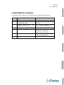
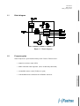
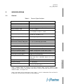
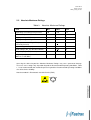
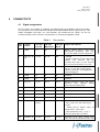
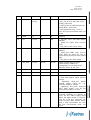
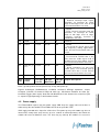
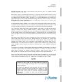
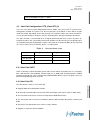
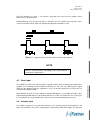
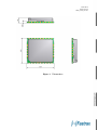
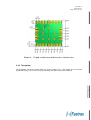
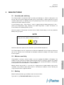
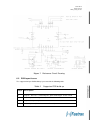
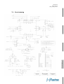
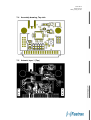
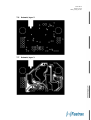
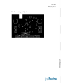
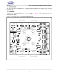
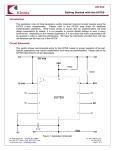
REV 1.6
TECHNICAL DESCRIPTION
Fastrax IT430 OEM GPS Receiver
This document describes the electrical connectivity and main
functionality of the Fastrax IT430 OEM GPS Receiver.
September 10, 2010
Fastrax Ltd.
2010-09-10
Page 2 of 43
IT430_Tech_doc.doc
TRADEMARKS
Fastrax is a registered trademark of Fastrax Ltd.
All other trademarks are trademarks or registered trademarks of their respective holders.
COPYRIGHT
© 2010 Fastrax Ltd.
DISCLAIMER
This document is compiled and kept up-to-date as conscientiously as possible. Fastrax Ltd.
cannot, however, guarantee that the data are free of errors, accurate or complete and,
therefore, assumes no liability for loss or damage of any kind incurred directly or indirectly
through the use of this document. The information in this document is subject to change
without notice and describes only generally the product defined in the introduction of this
documentation. Fastrax products are not authorized for use in life-support or safety-critical
applications. Use in such applications is done at the sole discretion of the customer. Fastrax
will not warrant the use of its devices in such applications.
2010-09-10
Page 3 of 43
IT430_Tech_doc.doc
CHANGE LOG
Rev.
Notes
Date
1.0
Initial documentation
2010-02-18
1.1
Added notes on power up and power removal; relaxed
operation temperature range between -40ºC and -30ºC;
increased module height to 1.85 mm, updated table 3
(added I/O type vs. operating mode); added note and
spec on ESD sensitivity and avoid ultrasonic exposure
2010-04-19
1.2
Updated power consumption and added notes on
internal regulator mode; added note on ESD sensitivity
of the antenna input; added out-of-band RF_IN power
spec to abs. max
2010-05-11
1.3
Added chapter on reset state. Clarified low power
operation modes (added APM; notes on PTF &
SiRFAware);
2010-06-04
1.4
Added two module variants, corrected volatile data RAM
clearing at reset; added Tape&Reel spec; added chapter
on Jammer Remover; clarified operating temperature
range down to -40… -30C with relaxed performance
2010-06-28
1.5
Corrected external pull up resistors requirement to
DR_I2C bus
2010-06-30
1.6
Changed accelerometer interrupt to EIT signal and EIT2
connection to GND; added operation notes on CGEE
usage and ROM patch; updated notes on host SPI and
I2C bus; added chapter on ABP; corrected some typos;
updated AP430 documents to rev B board; clarified
reset operation vs. ROM patch
2010-09-10
2010-09-10
Page 4 of 43
IT430_Tech_doc.doc
CONTENTS
_______________________________________________________________________
1
2
3
4
GENERAL DESCRIPTION............................................................................... 7
1.1
Block diagram....................................................................................... 8
1.2
Frequency plan ..................................................................................... 8
SPECIFICATIONS ........................................................................................... 9
2.1
General.................................................................................................. 9
2.2
Absolute Maximum Ratings ............................................................... 10
OPERATION.................................................................................................. 11
3.1
Operating modes ................................................................................ 11
3.2
Full on mode ....................................................................................... 11
3.2.1
Host port configuration ............................................................. 11
3.2.2
Power management system modes .......................................... 12
3.2.3
Self-Assistance - Client Generated EE usage .......................... 12
3.2.4
Patching ROM Firmware .......................................................... 13
3.2.5
Almanac Based Positioning ...................................................... 13
3.3
Hibernate state ................................................................................... 13
3.4
Reset state .......................................................................................... 14
CONNECTIVITY ............................................................................................ 15
4.1
Signal assignments ............................................................................ 15
4.2
Power supply ...................................................................................... 17
4.3
Host Port Configuration: RTS_N and CTS_N .................................... 19
4.3.1
Host Port UART ....................................................................... 19
4.3.2
Host Port SPI ........................................................................... 19
4.3.3
Host Port I2C ............................................................................ 20
4.4
ON_OFF control input ........................................................................ 20
4.5
Reset input.......................................................................................... 21
4.6
Antenna input ..................................................................................... 21
4.6.1
Active GPS antenna ................................................................. 22
4.6.2
Jamming Remover ................................................................... 22
4.7
Dead Reckoning I2C bus .................................................................... 22
4.8
Time Mark TM ..................................................................................... 23
4.9
WAKEUP ............................................................................................. 23
4.10 Interrupt inputs EIT and EIT2............................................................. 24
4.10.1 EIT ........................................................................................... 24
4.10.2 EIT2 ......................................................................................... 24
2010-09-10
Page 5 of 43
IT430_Tech_doc.doc
4.11 ELCK ................................................................................................... 24
4.12 TSYNC ................................................................................................. 24
4.13 Mechanical dimensions and contact numbering .............................. 24
4.14 Test points .......................................................................................... 26
4.15 Suggested pad layout ........................................................................ 27
5
MANUFACTURING ....................................................................................... 28
5.1
Assembly and soldering .................................................................... 28
5.2
Moisture sensitivity ............................................................................ 28
5.3
Marking ............................................................................................... 28
5.3.1
5.4
6
7
Module variants........................................................................ 29
Tape and reel ...................................................................................... 30
REFERENCE DESIGN................................................................................... 31
6.1
Reference circuit diagram.................................................................. 31
6.2
PCB layout issues .............................................................................. 32
AP430 APPLICATION BOARD ..................................................................... 34
7.1
Card Terminal I/O-connector ............................................................. 34
7.2
Bill of materials .................................................................................. 37
7.3
Circuit drawing ................................................................................... 39
7.4
Assembly drawing, Top side.............................................................. 40
7.5
Artwork, layer 1 (Top)......................................................................... 40
7.6
Artwork, layer 2 .................................................................................. 41
7.7
Artwork, layer 3 .................................................................................. 41
7.8
Artwork, layer 4 (Bottom) ................................................................... 42
2010-09-10
Page 6 of 43
IT430_Tech_doc.doc
COMPLEMENTARY READING
The following reference documents are complementary reading for this document:
Ref. #
File name
Document name
I
SiRFstarIV Brochure.pdf
SiRFstar IV Brochure
II
NMEA Reference Manual (CS129435-MA-1).pdf
NMEA
Manual
III
GSD4e OSP Manual
129291-DC-8).pdf
One Socket Protocol (OSP)
Interface Control Document
IV
Reflow_soldering_ profile.pdf
Soldering Profile
V
AN-452.pdf
Microwire™ Serial Interface;
National Semiconductor
Application Note AN-452
VI
39340011.pdf
The
I2C
Bus
Specification,
Philips Semiconductors
VII
SiRFLive User Manual.pdf
SiRFLive User Manual
(CS-
Protocol
Reference
2010-09-10
Page 7 of 43
IT430_Tech_doc.doc
1
GENERAL DESCRIPTION
The Fastrax IT430 is an OEM GPS receiver module, which provides the SiRFstar IV receiver (ref
I) functionality using the state of the art SiRF GSD4e chip (ROM variant). The module has ultra
small form factor 9.6x9.6 mm, height is 1.85 mm nominal (2.15 mm max). The Fastrax IT430
receiver provides low power and very fast TTFF together with weak signal acquisition and
tracking capability to meet even the most stringent performance expectations.
The module provides complete signal processing from antenna input to host port in either NMEA
messages (ref II) or in SiRF OSP binary protocol (ref III). The module requires a single power
2
supply VDD +1.8V. The host port is configurable to UART, SPI or I C during power up. Host data
and I/O signal levels are 1.8V CMOS compatible, inputs are 3.6V tolerable.
The SiRFstar IV provides a new feature called SiRFAware (also referenced as Micro Power
Management mode), which enables fast TTFF for Snap start mode while consuming only 500 uA
average current (typ.) in autonomous Hibernate state. The receiver does wakeup autonomously
to calibrate internal GPS time and to collect ephemeris data while maintaining 1 sec Snap fix
capability. The module supports also connectivity to optional external sensors for Dead
2
Reckoning like 3D-accelerometer on dedicated DR_I C bus.
The receiver is also optionally self-assisted since the Client Generated Extended Ephemeris
(CGEE) calculation is embedded in the software without any resources required from the host.
2
The CGEE data is stored on external serial EEPROM memory on the dedicated DR_I C bus (can
be optionally transferred to/from host).
The SiRFstar IV contains also a CW Jammer Remover, which will track and remove up to 8 CW
(Carrier Wave) type signals up to 80dBHz (equals to -90 dBm typ.) signal level.
The antenna input supports passive and active antennas and provides also an input for externally
generated antenna bias supply.
This document describes the electrical connectivity and main functionality of the Fastrax
IT430 OEM GPS Receiver module.
2010-09-10
Page 8 of 43
IT430_Tech_doc.doc
1.1
Block diagram
Figure 1
1.2
Block diagram
Frequency plan
Clock frequencies generated internally at the Fastrax IT430 receiver:
• 32768 Hz real time clock (RTC)
• 8 MHz switched mode regulator (when enabled by command)
• 16.369 MHz master clock (TCXO or crystal)
• 3142.96 MHz local oscillator of the RF down-converter
2010-09-10
Page 9 of 43
IT430_Tech_doc.doc
2
SPECIFICATIONS
2.1
General
Table 1
General Specifications
Receiver
GPS L1 C/A-code, SPS
Chip set & Tracking sensitivity
SiRF IV, GSD4e, -163 dBm
Channels
48
Update rate (default)
1 Hz max (fix rate configurable)
Supply voltage, VDD
+1.71… +1.89 V
Supply voltage ripple, VDD
54 mV(RMS) max @ f = 0… 3MHz
15 mV(RMS) max @ f > 3 MHz
Power consumption (note 1)
56 mW (Switcher mode) or 68 mW (LDO
mode) typ. @ VDD=1.8 V
Power consumption (Hibernate
state)
36 uW typical @ 1.8 V
Antenna net gain range
0…+25 dB
Antenna bias voltage VDD_ANT
+/- 5.5 V (externally generated)
Antenna bias current VDD_ANT
70 mA rated max
Storage temperature
-40ºC…+85ºC
Operating temperature
-40ºC…+85ºC (note 2)
Host port configuration
SPI (default), UART or I 2 C
Serial port protocol (UART)
NMEA (configurable to SiRF binary OSP)
Serial data format (UART)
8 bits, no parity, 1 stop bit
Serial data speed (UART)
4800 baud (configurable)
I/O signal levels
CMOS compatible: low state 0… +0.4 V max;
high state 0.75…1.0xVDD. Inputs are 3.6 V
tolerable
I/O output sink/source capability
+/- 2 mA max
I/O input leakage
+/- 10 uA max
TM output (1PPS)
200ms high pulse, rising
accuracy to GPS epoch
edge
+/-1
us
Note 1: Module boots for internal 1.2V LDO regulator mode. Internal Switcher mode
regulator reduces power consumption and requires a binary command from host to enable
Switcher mode, see chapter 4.2.
Note 2: Operation in the temperature range –40°C… –30°C is allowed but Time-to-First-Fix
performance and tracking sensitivity may be degraded.
2010-09-10
Page 10 of 43
IT430_Tech_doc.doc
2.2 Absolute Maximum Ratings
Table 2
Absolute Maximum Ratings
Item
Min
Max
unit
Operating and storage temperature
-40
+85
ºC
Power dissipation
-
200
mW
Supply voltage, VDD
-0.3
+2.2
V
Supply voltage, VDD_ANT
-5.5
+5.5
V
Supply current, VDD_ANT (must be
externally limited)
-
+150
mA
Input voltage on any input connection
-0.3
+3.6
V
ESD voltage (RF_IN, Machine Model)
-
+50
V
RF_IN input power (in band)
-
+10
dBm
RF_IN input power (out of band <1460
MHz or >1710 MHz)
-
+15
dBm
Stressing the device beyond the Absolute Maximum Ratings may cause permanent damage.
These are stress ratings only. Operation beyond the Recommended Operating Conditions, Table
1, is not recommended and extended exposure beyond the Recommended Operating Conditions
can affect device reliability.
Note that module is Electrostatic Sensitive Device (ESD).
2010-09-10
Page 11 of 43
IT430_Tech_doc.doc
3
OPERATION
3.1 Operating modes
After power up the IT430 module boots from the internal ROM to Hibernate state. The module
operation requires ON_OFF interrupt to wakeup for Normal (Navigation, Full on) mode. Modes of
operation:
• Full on (Navigation, Full Power)
o
Power management system modes
• Hibernate state
• Reset state
3.2 Full on mode
The module will enter Hibernate state after first power up with factory configuration settings. The
Navigation mode will start after waking up from Hibernate state in cold start mode by sending
ON_OFF signal interrupt pulse from host. Power consumption will vary depending on the amount
of satellite acquisitions and number of satellites in track. This mode is also referenced as Full on,
Full Power or Navigation mode.
Navigation is available and any configuration settings are valid as long as the VDD power supply
is active. When the VDD is powered off, settings are reset to factory configuration and receiver
performs a cold start on next power up.
VDD supply is intended to be kept active all the time and navigation activity is suggested to be
controlled to low quiescent Hibernate state via ON_OFF control input. See also chapter 3.3 and
4.2.
3.2.1 Host port configuration
2
User can select the host port configuration between UART, SPI (slave) and I C (master/slave)
during power up boot. The port selection is not intended to be changed dynamically but only set
once at power up. Default host port is SPI and other host port configurations requires external
pull down or pull up resistor at CTS_N and RTS_N signals, see chapter 4 for details.
Default protocol for host communication is NMEA (ref II) 4800 baud. Protocol is switchable to
SiRF binary OSP (One Socket Protocol, ref III) by NMEA protocol command $PSRF100.
Default NMEA message configuration: $GPGGA, $GPGSA and $GPRMC rate every second (in
this order) and $GPGSV messages (can be 1… 4) every 5 seconds (sent after $GPGSA
message). Message output and rate can be configured by NMEA message $PSRF103 (ref II).
2010-09-10
Page 12 of 43
IT430_Tech_doc.doc
3.2.2 Power management system modes
The IT430 module supports also SiRF operating modes for reduced average power consumption
TM
TM
(ref III) like Adaptive TricklePower , Advanced Power Management, Push-to-Fix
and
TM
SiRFAware modes:
1. Adaptive TricklePower (ATP): In this mode the receiver stays at Full on power state for
200… 900ms and provides a valid fix. Between fixes with 1… 10 sec interval the receiver
stays in Hibernate state. ATP mode is configurable with SiRF binary protocol message
ID151 (ref III). The receiver stays once in while in Full on power mode automatically (typ.
every 1800 sec) to receive new ephemeris data from rising satellites or if received signal
levels drop below certain level.
2. Advanced Power Management (APM): APM allows power savings while ensuring that the
quality of the solution is maintained when signal levels drop. APM does not engage until
all necessary information is received. Host can configure e.g. number of APM cycles
(continuous or up to 255), time between fixes (10… 180 sec), Power duty cycle (5…
100%) and max position error. Rest of the time the receiver stays in Hibernate state. This
mode is configurable with SiRF binary protocol message ID53 (ref III).
3. Push-to-Fix (PTF): In this mode the receiver is configured to wake up periodically, typically
every 1800 sec (configurable range 10… 7200 sec), for position update and to collect
new ephemeris data from rising satellites. Rest of the time the receiver stays in
Hibernate state. When position update is needed, the host can wake up the receiver by
ON_OFF control input interrupt (pulse low-high-low >90us after which the receiver
performs either Snap or Hot start and a valid fix is available within 1… 8 seconds typ.
This mode is configurable with SiRF binary protocol message ID151 & 167 (ref III).
4. SiRFAware (aka Micro Power Management mode, MPM): In this mode the receiver is
configured to wake up periodically for 18 sec, typically every 1800 sec, to collect new
ephemeris data from rising satellites, and also every 60 seconds for 250 ms to calibrate
internal navigation state and GPS time estimate. Rest of the time the receiver stays in
Hibernate state and module achieves 0.5 mA typ. average current drain. The host wakes
up the receiver by ON_OFF control input interrupt (pulse low-high-low >90us) to Full on
power mode after which the receiver performs Snap start and a valid fix is available
within 1 second typ. After valid fix, operation can return back to Micro Power
Management mode by re-sending the configuration binary message from host. This
mode is configurable with SiRF OSP (One Socket Protocol) binary protocol message
MID218 (ref III).
These power management modes are also configurable with SiRF OSP binary protocol message
MID 218, Power Mode Request (ref III). Note that position accuracy is somewhat degraded in
power management modes when compared to full power operation.
3.2.3 Self-Assistance - Client Generated EE usage
The IT430 module supports Client Generated Extended Ephemeris (CGEE), which allows fast
TTFF 10 sec typ for 3 days. The CGEE data is generated internally from satellite ephemeris as a
background task and thus host should allow the IT430 to navigate and to collect ephemeris from
as many satellites as possible before entering Hibernate state.
The CGEE feature requires that power supply is kept active all the time and that an external 1
2
Mbit EEPROM connected to DR_I C bus for CGEE data storage (see chapter 4.7). A command
2010-09-10
Page 13 of 43
IT430_Tech_doc.doc
is also required from host to enable EE storage to EEPROM ($PSRF120,F,R*30<CR><LF> or
OSP binary message ID 232, Sub ID 253; contact Fastrax support for details).
The CGEE data can be also stored optionally to host (contact Fastrax support for availability and
details).
3.2.4 Patching ROM Firmware
The firmware that is associated with IT430 is executed for internal ROM memory. It is a normal
practice that firmware patches may be provided from time to time in order to address ROM
firmware issues as a method of implementing bug fixes. Patch firmware (max. size 24 kB) and
downloading tools are available via Fastrax support. Patch can be stored on external EEPROM
2
at DR_I C bus or at host. Note that power down will clear internal patch RAM and thus after
power up the patch must be up either re-loaded from host or re-issued from external EEPROM
by two binary OSP messages sent from host (contact Fastrax support for suggested procedure).
3.2.5 Almanac Based Positioning
User can enable so called Almanac Based Positioning (ABP, see NMEA command $PSRF103 or
OSP command ID 136), which allows fast cold starts TTFF 22 sec typ. since broadcast
ephemeris data is not need from visible satellites but the factory set (or broadcast or pushed)
Almanac data is used for positioning. When broadcast ephemeris data gets available from visible
satellites, the navigation will use automatically more precise ephemeris data for positioning.
When ABP is enabled, the navigation message (e.g. NMEA $GPRMC) will indicate when ABP
positioning is being used in navigation ($GPRMC: Mode=R).
The positioning accuracy is in the order of few hundred meters to kilometers and is usable mainly
to coarse positioning (e.g. to find out in which country/state/district the receiver is located).
Position accuracy is also expected to degenerate when actual Ephemeris/Almanac starts to differ
from the factory set Almanac data in power down/on cycles. Host may try to overcome this
problem by either keeping the power supply active all the time using Hibernate or by polling latest
broadcast Almanac from the module (by OSP Message ID 146) prior power down and then
pushing the Almanac back to module (by OSP Message ID 130) at next power up after waking
up from Hibernate state. Note the Almanac data broadcast takes 12.5 minutes and thus allow the
module to navigate in Full on mode at least for this period.
3.3 Hibernate state
Hibernate state means a low quiescent (20uA typ.) power state where only the internal I/O Keep
Alive, non-volatile RTC, patch RAM and backup RAM block is powered on. Other internal blocks
like digital baseband and RF are internally powered off. The main supply input VDD shall be kept
active all the time, even during Hibernate state. Waking up from and entering in to Hibernate
state is controlled by host interrupt at ON_OFF control input (rising edge toggle low-high-low
>90us).
During Hibernate state the I/O Keep Alive is still active, thus I/O signals keep respective states
except TX and RX signals, which are configured to high input impedance state.
2010-09-10
Page 14 of 43
IT430_Tech_doc.doc
The receiver wakes up from Hibernate state on the next ON_OFF interrupt (at rising edge) using
all internal aiding like GPS time, Ephemeris, Last Position etc. resulting to a fastest possible
TTFF in either Hot or Warm start modes.
3.4 Reset state
Reset state is entered internally after power up until the internal RTC clock wakes up after which
internal reset state is relaxed and module boots to Hibernate state. Host can override reset state
via RESET_N (pin 12) input, low state active. Normally external reset override is not required but
if power shall be removed abruptly see chapter 4.2 for reset suggestion.
Note that reset clears data RAM content, e.g. downloaded ROM patch code. User can overcome
this problem by using patch storage to external EEPROM and thus the module is able to re-issue
patch code header back to internal patch RAM after waking up from successive Hibernate state.
Backup RAM content is not cleared and thus fast TTFF is possible after reset and system
configuration settings are sustained.
2010-09-10
Page 15 of 43
IT430_Tech_doc.doc
4
CONNECTIVITY
4.1 Signal assignments
The I/O signals are available as soldering (castellated) pads on the bottom side of the module.
These pads are also used to attach the module on the motherboard. All I/O signal levels are 1.8V
CMOS compatible and inputs are 3.6V tolerable. All unconnected I/O signals can be left
unconnected when not used, unless instructed to use external pull up/down resistor.
Table 3
Connections
Con
tact
Signal
name
I/O type
Full on
I/O type
Hibernate
I/O type
Reset
Signal description
1
VDD
P,I
P,I
P,I
Power supply input +1.8V nom.
De-couple externally with e.g.
4.7uF low ESR ceramic capacitor.
2
DR_I2C_D
IO
S,C,B
S,C,B
HZ
- GPIO0
- Dead reckoning I 2 C host bus data
(SDA). Use external pull up
resistor when bus is used. Can be
left unconnected when not used.
3
VDD_ANT
P,I
P,I
P,I
Antenna bias power supply input
up to +/-5.5V. De-couple signal
further externally, see Application
Circuit Diagram.
4
GND
G
G
G
Ground
5
GND
G
G
G
Ground
6
RF_IN
A,I,O
A,I,O
A,I,O
Analog Antenna input (50 ohm),
Antenna
bias
voltage
output
(filtered from VDD_ANT)
7
GND
G
G
G
Ground
8
GND
G
G
G
Ground
9
GND
G
G
G
Ground
10
GND
G
G
G
Ground
11
CTS_N
S,C,B,
PD(a)
S,C,B, PD
HZ
- GPIO6
- SPI_CLK slave SPI clock input
(CLK)
- UART_CTS_N UART Clear to
Send (CTS), active low
- Host port boot strap, see 4.3
Pull up externally for UART.
12
RESET_N
C,I,PU
C,I,PU
C,I,PU
External reset input, active low.
Can be left unconnected when not
2010-09-10
Page 16 of 43
IT430_Tech_doc.doc
used.
13
RTS_N
S,C,B,
PU(a)
S,C,B, PU
HZ
- GPIO7
- SPI_SS_N slave SPI chip select
(CS#), active low
- UART_RTS_N UART Request to
Send (RTS), active low
- Host port boot strap, see 4.3
Can be left unconnected when not
used.
14
GND
G
G
G
Ground
15
TX
S,C,B
HZ
HZ
- SPI_DO slave SPI data output
(MISO)
- UART_TX UART data transmit
(TX)
- I2C_CLK I²C bus clock (SCL)
16
RX
S,C,B
HZ
HZ
- SPI_DI slave SPI data input
(MOSI)
- UART_RX UART data receive
(RX). Must be driven by host or
use external pull up resistor (UART
RX).
- I2C_DIO I²C bus data (SDA)
17
ON_OFF
S,C,B
S,C,B
S,C,B
Power control input used to
command the module On
(Navigation) or Off (Hibernate).
Must be driven by the host.
18
GND
G
G
G
Ground
19
GND
G
G
G
Ground
20
TM
S,C,B
S,C,B
HZ
- GPIO5
- Time mark output signal (default
1PPS)
- Optionally GPS_ON, power
control output signal for e.g.
external LNA bias control.
- Optionally RTC_CLK, buffered
RTC clock output. Can be left
unconnected when not used.
21
WAKEUP
C,O
C,O
C,O
Wakeup output for control of
external regulator, e.g. battery to
1.8V for the VDD supply input
when full power mode is entered.
Can be used also externally for
active antenna bias control, active
high = high current/bias on. Can
be left unconnected when not
used.
2010-09-10
Page 17 of 43
IT430_Tech_doc.doc
22
EIT
S,C,B
S,C,B
HZ
- GPIO4
- External interrupt input signal.
Provides an interrupt on either
high or low logic level. Can be left
unconnected when not used.
23
EIT2
S,C,B
S,C,B
HZ
- GPIO8
- EIT2 external interrupt input #2.
Provides an interrupt on either
high or low logic level or edgesensitive interrupt. Connect to
GND when not used.
24
GND
G
G
G
Ground
25
ECLK
S,C,B
S,C,B
HZ
- GPIO3
- Reserved for ECLK clock input
for frequency aiding applications.
Can be left unconnected when not
used.
26
TSYNC
S,C,B
S,C,B
HZ
- GPIO2
- Reserved for TSYNC that is the
time transfer strobe input used in
A-GPS precise time aiding. Can be
left unconnected when not used.
27
DR_I2C_C
LK
S,C,B
S,C,B
HZ
- GPIO1
- Dead reckoning I²C host bus
clock (SCL). Use external pull up
resistor when bus is used. Can be
left unconnected when not used.
28
GND
G
G
G
Ground
Con
tact
Signal
name
I/O type
Full on
I/O type
Hibernate
I/O type
Reset
Signal description
Notes: (a) Pull Up/down resistor present only shortly after power up.
Legend: A=Analogue, B=Bidirectional, C=CMOS, G=Ground, HZ=High Impedance, I=Input,
O=Output, P=Power, PU=Internal Pullup 86 kohm typ., PD=Internal Pulldown 91 kohm typ.,
S=Schmitt Trigger (when Input). Note that with Birectional I/O the firmware has control for input
vs. output I/O type depending on the firmware function.
4.2 Power supply
The IT430 module requires only one power supply VDD. Keep the supply active all the time in
order to keep the non-volatile RTC & RAM active for fastest possible TTFF.
VDD supply intended to be kept alive all the time. First power up may take 300ms typ. due to
internal RTC startup time (may increase up to 5 seconds at cold temperature) after which the
module will enter to Hibernate state. The host may try wakeup the module via successive
2010-09-10
Page 18 of 43
IT430_Tech_doc.doc
ON_OFF interrupts sent every second until the host port messages are outputted and/or
WAKEUP output is at high state.
When power supply is intended to be removed, it is suggested that prior power removal a serial
message in binary (MID 205) or NMEA format ($PSRF117,16*0B<CR><LF>) is sent to module to
shut down firmware operations orderly. Otherwise e.g. external EEPROM may get corrupted if
power down happens in the middle of EEPROM writing, which may increase in TTFF. If external
EEPROM is also used for ROM patch code, the abrupt power removal may cause patch code
corruption that may end to system failure.
Second option for orderly shutdown is to send ON_OFF interrupt prior VDD removal. Operations
shutdown may take anything between 10 to 900 ms depending upon operation in progress and
messages pending and hence is dependent upon serial interface speed and host port type.
If it is likely that VDD supply will be removed abruptly, suggestion is to add external voltage
monitor to detect under voltage condition below 5% nominal supply voltage and to drive
RESET_N signal to reset condition (low state). This important especially when external EEPROM
or data storage at host is used. VDD supply off-time is suggested to be over 10 seconds to next
power up in order to clear all internal backup RAM content and to minimize risk for wrong backup
data.
Main power supply VDD current varies according to the processor load and satellite acquisition.
Typical VDD peak current is 56 mA (typ.) during waking for Full on power up. Typical VDD
current in low power Hibernate state is 20uA. The external power supply can be using dual
low/high current modes, which can be controlled via the WAKEUP output signal (high current =
WAKEUP high) as indication when full power is required by the module. The external power
supply should be able to provide full current to VDD within 9 ms after WAKEUP low-to-high
transition.
The internal 1.2V regulator is powered from VDD supply and it boots for LDO mode. The internal
1.2V power supply includes also Switcher mode regulator (f = 8 MHz). The host may reduce
power drain by enabling the Switcher mode via sending a binary message from the host
(Message ID 178 TrackerIC, Sub ID 2 TrackerConfig; contact Fastrax support for details).
By-pass the VDD supply input by a low ESR ceramic de-coupling capacitor (e.g. 4.7 uF) placed
nearby VDD pin to ensure low ripple voltage at VDD. Ensure that the VDD supply ripple voltage
is low enough: 54 mV(RMS) max @ f = 0… 3MHz and 15 mV(RMS) max @ f > 3 MHz.
NOTE
VDD supply is intended to be active all the time. Abrupt
removals of VDD supply are not suggested and if required,
use an external voltage detector to force reset at VDD under
voltage conditions.
De-couple the VDD input externally with e.g. 4.7uF low ESR
ceramic capacitor connected to GND. The module has also
internal a low ESR (~0.01 ohm) by-pass capacitor at VDD
supply input. Ensure that the external regulator providing
VDD supply is suitable for loads with low ESR ceramic
capacitors.
2010-09-10
Page 19 of 43
IT430_Tech_doc.doc
VDD supply ripple voltage: 54 mV(RMS) max @ f = 0… 3MHz
and 15 mV(RMS) max @ f > 3 MHz.
4.3 Host Port Configuration: RTS_N and CTS_N
2
User can select the host port configuration between UART, SPI (slave) and I C (master/slave)
during power up boot. At system reset, the host port pins are disabled, so there will be no port
conflict occurring. Depending on the host port type, the software enables the correct port drivers,
sets up the port hardware, configures the pins according to the port type and begins operations.
The port selection is not intended to be changed dynamically but only set once at power up.
Default host port is SPI (selected by internal pull up/down resistors that are present during power
up) and other host port configurations requires connection of external pull down (to 0V) or pull up
(to 1.8V) resistor at CTS_N and RTS_N pins, see table below.
Table 4
Host port boot strap
Host port
RTS_N
CTS_N
UART
-
Pull up 10 kohm
SPI (default)
-
-
I2C
Pull down 10 kohm
-
4.3.1 Host Port UART
UART is normally used for GPS data reports and receiver control. Serial data rates are selectable
from 1200 baud to 1.8432 Mbaud. Default baud rate is 4800 baud; default protocol is NMEA
(protocol and baud rate can be configured by NMEA $PSRF100 message). RX signal can be left
not connected (floating) when not used.
4.3.2 Host Port SPI
The host interface SPI is a slave mode SPI:
■ Supports both SPI and Microwire formats
■ An interrupt is provided when the transmit FIFO and output serial register (SR) are both empty
■ The transmitter and receiver each have independent 1024B FIFO buffers
■ The transmitter and receiver have individual software-defined 2-byte idle patterns of 0xA7 and
0xB4
■ SPI detects synchronization errors and is reset by software
■ Supports a maximum clock of 6.8MHz.
2010-09-10
Page 20 of 43
IT430_Tech_doc.doc
The SPI bus is a synchronous serial data link and a ‘de facto’ standard named by Motorola. For
further information see e.g. Wikipedia:
http://en.wikipedia.org/wiki/Serial_Peripheral_Interface_Bus.
Microwire is a restricted subset of SPI and a trademark of National Semiconductor. For details
see e.g. http://www.national.com/an/AN/AN-452.pdf (ref V).
4.3.3 Host Port I2C
The I²C host port interface supports:
■ Default speed is 100kbps, configurable to 400kbps max (by OSP Message ID 178, Sub ID 2)
■ Default operating mode is multi-master (configurable to slave, OSP Message ID 178, Sub ID 2):
■ Transmit side operates as master by seizing the I²C bus when detected idle
■ Receive side operates as a slave when another master seizes bus and transmits to this
address
2
■ Default I C address values are (configurable by OSP Message ID 178, Sub ID 2):
■ RX 0x60, TX 0x62
■ Individual transmit and receive FIFO lengths of 64B
The operation of the I²C in multi-master mode with a master transmit and slave receive mimics a
UART operation, where both module and host can independently freely transmit. The I²C bus
operation is specified in detail including evaluating tools, application notes and drivers by Philips
Semiconductors, see http://www.nxp.com/acrobat_download2/literature/9398/39340011.pdf (ref
VI).
NOTE
When host port is configured to I²C bus use external pull up
resistors (e.g. 2.2 kohm to +1.8… +3.6 V) at both signals.
4.4 ON_OFF control input
The ON_OFF control input must be used by the host to wakeup the module after first power up
and to control the receiver activity between Normal and Hibernate states and also to generate
interrupt in Push-to-Fix and SiRFAware modes of operation.
The module will boot to Hibernate state after power up. First ON_OFF interrupt wakes up the
module for Normal (Navigation) operation. Consequent ON_OFF interrupts switch the operation
mode between Hibernate and Navigation modes.
The ON_OFF interrupt is generated by rising edge of a low-high-low pulse, which should be
longer than 90us and less than 1s (suggestion is abt. 100ms pulse length). Do not generate
2010-09-10
Page 21 of 43
IT430_Tech_doc.doc
ON_OFF interrupts less than 1 sec intervals. Especially take care that any multiple switch
bounce pulses are filtered out.
During Hibernate state the I/O Keep Alive is still active, thus I/O signals keep respective states
except TX and RX signals, which are configured to high input impedance state.
Figure 2
Suggested ON_OFF Hibernate control timing diagram.
NOTE
Do not generate multiple ON_OFF interrupts less than 1 sec
intervals. Especially filter out multiple pulses generated by a
mechanical switch bounce.
4.5 Reset input
The RESET_N (active low) signal provides external override of the internally generated power
up/down reset. Normally external control of RESET_N is not necessary. When power supply
VDD may be abruptly removed, suggestion is to use externally generated reset by means of
external VDD voltage monitor.
When RESET_N signal is used, it will force volatile RAM data loss (e.g. ROM patch code). NonVolatile Backup RAM content is not cleared and thus fast TTFF is possible after reset. The input
has internal pull up resistor 86 kohm typ. and leave it not connected (floating) if not used.
4.6 Antenna input
The module supports passive and active antennas. The antenna input RF_IN impedance is 50
ohms and it provides also a bias supply low-pass filtered form VDD_ANT supply. The RF input
2010-09-10
Page 22 of 43
IT430_Tech_doc.doc
signal path contains first a SAW band-pass filter, which provides good out-of-band protection
against GPS blocking caused by possible near-by wireless transmitters.
Note that antenna input is ESD sensitive. With passive antennas the ESD performance can be
improved by connecting VDD_ANT supply input to GND. Also an external TVS diode with low
capacitance (<0.5pF, e.g. Infineon ESD0P2RF) can be used to improve RF-input ESD capability.
NOTE
With Passive antennas leave VDD_ANT not connected or
connect to GND.
4.6.1 Active GPS antenna
The customer may use an external active GPS antenna when antenna cable loss exceeds > 1dB.
It is suggested the active antenna has a net gain including cable loss in the range from +7 dB to
+25 dB. Specified sensitivity is measured with external low noise (NF<1dB, G>15dB) amplifier,
which gives about 2dB advantage in sensitivity when compared to a passive antenna.
An active antenna requires certain bias voltage, which can be supplied externally via VDD_ANT
supply input. De-couple externally the VDD_ANT input; see the application circuit diagram in
chapter 6. The external bias supply must provide limitation of the max current below 150mA
during e.g. antenna signal short circuit condition.
When the module is in Hibernate state, the antenna bias can be switched off externally by using
WAKEUP signal output to switch off VDD_ANT supply, see e.g. Application Circuit Diagram.
NOTE
With Active GPS Antenna provide externally VDD_ANT
supply suitable for the active antenna used. The VDD_ANT
supply must provide also short circuit protection externally,
rated current 70mA, abs. max. 150mA.
4.6.2 Jamming Remover
Jamming Remover (aka CW Detection) is an embedded HW block that detects, tracks and
removes up to 8 pcs CW (Carrier Wave) type signals up to 80 dBHz (-90 dBm) signal levels. The
usage requires an OSP binary command Message ID 220 (CW Configuration) to enable.
Jamming Remover can be used for detecting and solving EMI problems in the customer’s system
and it is effective against e.g. narrow band clock harmonics. Use PC utility SiRFLive to indicate
and detect CW EMI signals, see SiRFLive user manual (ref VII) for details.
Note that Jamming Removal is not effective against wide band noise (e.g. from host CPU
memory bus), which increases effective noise floor and reduces GPS signal levels.
4.7
Dead Reckoning I2C bus
2
The DR_I C bus (master) provides optional connectivity to the following devices:
2010-09-10
Page 23 of 43
IT430_Tech_doc.doc
■ Optional Dead Reckoning sensors (e.g. 3-D Accelerometer)
■ Optional connectivity to EEPROM for Client Generated Extended Ephemeris (CGEE) data
storage (see chapter 3.2.3).
■ Optional ROM patch code storage to EEPROM and upload to IT430 (see chapter 3.2.3).
The accelerometer MEMS sensor provides stationary detection, which allows to reduce the
position spread when stationary with weak GPS signals e.g. indoors. Other features will follow
like Pedestrian DR (contact Fastrax support for details). When MEMS sensor is used connect
also the sensor’s INT output to IT430’s EIT input. The bus signals require external pull up
resistors 2.2kohm on both signals and can be left not connected when not used.
DR I²C interface supports:
■ Common sensor formats (Kionix, KXTF9-4100 device)
■ Common EEPROM data formats (STMicroelectronics, M24M01, 1 Mbit device)
■ Typical data lengths (command + in/data out) of several bytes
■ Standard I²C bus maximum data rate 400kbps
■ Minimum data rate 100kbps
NOTE
When used the DR I²C bus require external pull up resistors
2.2kohm (to +1.8… +3.6 V) at both signals.
4.8
Time Mark TM
The TM output signal provides pulse-per-second (1PPS) output pulse signal for timing purposes.
Pulse length (high state) is 200ms about 1us accuracy synchronized at rising edge to full UTC
second.
The firmware may support optionally other output functions from TM signal, like GPS_ON output
for e.g. external LNA power control or RTC_CLK, which outputs buffered RTC clock signal at
32768 Hz; contact Fastrax support for details.
4.9
WAKEUP
The WAKEUP output signal provides indication to e.g. external power supply when full power is
required by the module. Polarity is active high = high current mode. The external power supply
should be able to provide full current to VDD within 9ms after WAKEUP low->high transition.
WAKEUP signal can be also used externally to switch off the Active Antenna Bias supply voltage
(VDD_ANT) during Hibernate state; polarity is active high = VDD_ANT active.
2010-09-10
Page 24 of 43
IT430_Tech_doc.doc
4.10 Interrupt inputs EIT and EIT2
The EIT and EIT2 are external, level sensitive interrupt inputs. EIT2 pin is also configurable as an
edge-sensitive input. Both pins are disabled at initial power-up and usage is configured by the
software.
Either pin can be used as a source of a level sensitive interrupt to wake-up the module from
Hibernate low-power state. This feature allows external sensors, e.g. gyro, accelerometer,
compass, etc., to provide an interrupt when a change of state is detected.
4.10.1
EIT
The EIT signal is only available as a level triggered interrupt. Either high and low levels are
programmable as the active condition on EIT, this is also the same as the EIT2 pin. The input can
be left not connected when not used.
In order to recognize a level triggered interrupt, the EIT pin input must remain in a given state for
a long enough time for the RTC re-timing process to sample the level, 3 RTC_CLK ticks are
sufficient, about 90µs. At system reset, the EIT pin is disabled.
4.10.2
EIT2
The EIT2 signal is available as either an edge triggered or a level triggered interrupt, while EIT is
only available as a level triggered interrupt. Either high or low levels or either rising edge or falling
edge are programmable as the active condition on EIT2. The input is suggested to be connected
to GND when not used.
In order to recognize a level or an edge, the pin input must remain in a given state for a long
enough time for the RTC re-timing process to sample the level, 3 RTC_CLK ticks are sufficient,
about 90µs. At system reset, the EIT2 pin is disabled.
4.11 ELCK
The ECLK is reserved for external clock input with special variant for A-GPS frequency aiding.
The input can be left not connected when not used.
4.12 TSYNC
TSYNC input is reserved for external time aiding with a special variant used for A-GPS. The input
can be left not connected when not used.
4.13 Mechanical dimensions and contact numbering
Module size is square 9.6 mm (width/length) and 1.85 mm (height, 2.15 mm max). General
tolerance is ±0.3 mm. Note pin 1 polarity mark on the lower left corner on the shield.
2010-09-10
Page 25 of 43
IT430_Tech_doc.doc
Figure 3
Dimensions
2010-09-10
Page 26 of 43
IT430_Tech_doc.doc
Figure 4
I/O pad numbering and dimensions, bottom view.
4.14 Test points
On the bottom side of the module there are also test points TP1… TP8, which are reserved for
production testing. Leave these test points floating (not connected) and unsoldered.
2010-09-10
Page 27 of 43
IT430_Tech_doc.doc
4.15 Suggested pad layout
Figure 5
Suggested pad layout and occupied area, top view. Suggested
paste mask openings equal pad layout.
2010-09-10
Page 28 of 43
IT430_Tech_doc.doc
5
MANUFACTURING
5.1 Assembly and soldering
The IT430 module is intended for SMT assembly and soldering in a Pb-free reflow process on
the top side of the PCB. Suggested solder paste stencil height is 150um minimum to ensure
sufficient solder volume. If required paste mask pad openings can be increased to ensure proper
soldering and solder wetting over pads.
Use pre-heating at 150… 180 ºC for 60… 120 sec. Suggested peak reflow temperature is 235…
245ºC (for SnAg3.0Cu0.5 alloy). Absolute max reflow temperature is 260ºC. For details see
Fastrax document ‘Soldering Profile’ (ref IV).
Note that module is Electrostatic Sensitive Device (ESD). Rated voltage is 50V max (Machine
Model) at RF_IN signal.
NOTE
Note that module is Electrostatic Sensitive Device (ESD),
rating 50V max (Machine Model) at RF_IN.
Avoid also ultrasonic exposure due to internal crystal and SAW components.
The IT430 module meets the requirements of Directive 2002/95/EC of the European Parliament
and of the Council on the Restriction of Hazardous Substance (RoHS). For details contact
Fastrax support.
5.2 Moisture sensitivity
IT430 module is moisture sensitive at MSL 3 (see the standard IPC/JEDEC J-STD-020C). The
module must be stored in the original moisture barrier bag or if the bag is opened, the module
must be repacked or stored in a dry cabin (according to the standard IPC/JEDEC J-STD-033B).
Factory floor life in humid conditions is 1 week for MSL 3.
Moisture barrier bag self life is 1 year; thus it is suggested to assemble modules prior self life
expiration. If the moisture barrier bad self life is exceeded, the modules must be baked prior
usage; contact Fastrax support for details.
5.3
Marking
Module marking includes type and batch code and serial number.
Type code is e.g. IT430-400S-SGT-3595 (may vary), where
2010-09-10
Page 29 of 43
IT430_Tech_doc.doc
•
IT430 is module type code for IT430
•
400 is firmware (SDK) revision 4.0.0 and S is incremental firmware release revision (may
vary)
•
SGT is firmware feature set (Basic BSC or Signature SGT available, see 5.3.1)
•
3595 is BOM (Bill-of-Materials) revision code (may vary)
Batch code is e.g.100208 (may vary), where
•
1 is factory code
•
0 is last digit of the year (e.g. 2010)
•
02 is month (e.g. February)
•
08 is incremental number of the production batch during the month
Serial number is unique for each module having 10 digits including tester code, last two digits of
the year, julian date code and incremental number.
5.3.1 Module variants
The IT430 module is available in two variants based on firmware feature set. Note that by default
IT430 is shipped with Signature feature set and Basic feature set variant is available only on
request.
•
•
IT430-sssr-BSC Basic feature set (available only on request; sssr = FW revision):
o
CW Jammer Remover
o
Embedded Client and Server generated EE support
o
TricklePower, APM and Push-to-Fix low power modes
o
HW support only for default LDO mode (no Switcher coil in HW)
IT430-sssr-SGT Signature feature set adds the following in addition to Basic feature set:
o
SiRFAware (Micro Power Management) 500 uA low power state
o
Support for Almanac Based Navigation
o
AGPS support
o
SBAS/WAAS support
o
MEMS sensor support: 3-D Accelerometer, Stationary Detection
o
HW support for both LDO and Switcher mode (Switcher coil included in HW)
2010-09-10
Page 30 of 43
IT430_Tech_doc.doc
5.4 Tape and reel
One reel contains 500 modules.
Figure 6
Tape and reel specification
2010-09-10
Page 31 of 43
IT430_Tech_doc.doc
6
REFERENCE DESIGN
The idea of the reference design is to give a guideline for the applications using the OEM GPS
module. In itself it is not a finished product, but an example that performs correctly.
In the following two chapters the reader is exposed to design rules that he should follow, when
designing the GPS receiver in to the application. By following the rules one end up having an
optimal design with no unexpected behavior caused by the PCB layout itself. In fact these
guidelines are quite general in nature, and can be utilized in any PCB design related to RF
techniques or to high speed logic.
6.1 Reference circuit diagram
The following picture describes a minimum connectivity for a typical autonomous navigation
application. It consists of the IT430 module, which is powered by the main VDD supply (+1.8 V).
The external by-pass capacitor C1 is used to de-couple the VDD supply pin.
No back up supply is required. Instead keep the main supply VDD active all the time and use the
ON_OFF control input to switch between Navigation and Hibernate operation modes. WAKEUP
signal can be used for external regulator mode control for full power state. WAKEUP signal can
be also used to drive external antenna bias VDD_ANT (+3.3 V typ.) voltage switch (Q1) during
Normal/Hibernate modes. L1 and C2 provide Additional RF decoupling to VDD_ANT supply.
The host port is configured to UART by the pull up resistor R5. Serial port TX output is connected
to host UART input. RX input connection to host UART output is required when sending
commands to IT430. ON_OFF input must be driven by the host to wakeup the module from
Hibernate state after first power up. Optional connectivity for host includes TM signal for timing
purposes.
2
Optional connectivity includes an accelerometer sensor and an EEPROM on DR_I C bus for
stationary detection (later Pedestrian Dead Reckoning) and for Extended Ephemeris or ROM
patch code data storage, respectively. Use external pull up resistors 2.2kohm at bus signals
when bus is used.
Note that all I/O signal levels are CMOS 1.8V compatible and inputs are 3.6 V tolerable.
Some I/O signals have series resistors 47… 220 ohm, which are intended for RF-decoupling
purposes to improve rejection to internally generated EMI that may leak to nearby GPS antenna.
If GPS antenna is away > 10cm from module and/or I/O signals are routed under ground plane
these series resistor may be omitted.
2010-09-10
Page 32 of 43
IT430_Tech_doc.doc
Figure 7
Reference Circuit Drawing
6.2 PCB layout issues
The suggested 4-layer PCB build up is presented in the following table.
Table 5
Suggested PCB build up
Layer
Description
1
Signal + RF trace + Ground plane with solid copper under IT430
2
Ground plane for signals and for RF trace
3
Signals and power planes
4
Ground plane (also short traces allowed)
2010-09-10
Page 33 of 43
IT430_Tech_doc.doc
Routing signals directly under the module should be avoided. This area should be dedicated to
keep-out to both traces and assigned to ground plane (copper plane), except for via holes, which
can be placed close to the pad under the module. If possible, the amount of VIA holes
underneath the module should be minimized.
For a multi-layer PCB the first inner layer below the IT430 is suggested to be dedicated for the
ground plane. Below this ground layer other layers with signal traces are allowed. It is always
better to route very long signal traces in the inner layers of the PCB. In this way the trace can be
easily shielded with ground areas from above and below.
The serial resistors at the I/O should be placed very near to the IT430 module. In this way the
risk for the local oscillator leakage is minimized. For the same reason by-pass capacitors C1 and
C2 should be connected very close to the module with short traces to IO contacts and to the
ground plane. Place the GND via hole as close as possible to the capacitor.
Connect the GND soldering pads of the IT430 to ground plane with short traces (thermals) to via
holes, which are connected to the ground plane. Use preferably one via hole for each GND pad.
The RF input should be routed clearly away form other signals, this minimizes the possibility of
interference. The proper width for the 50 ohm transmission line impedance depends on the
dielectric material of the substrate and on the height between the signal trace and the first ground
plane. With FR-4 material the width of the trace shall be two times the substrate height.
A board space free of any traces should be covered with copper areas (GND). In this way, a solid
RF ground is achieved throughout the circuit board. Several via holes should be used to connect
the ground areas between different layers.
Additionally, it is important that the PCB build-up is symmetrical on both sides of the PCB core.
This can be achieved by choosing identical copper content on each layers, and adding copper
areas to route-free areas. If the circuit board is heavily asymmetric, the board may bend during
the PCB manufacturing or reflow soldering. Bending may cause soldering failures and reduce
end product reliability.
The AP430 Application Board layout described in next chapter can be also used as layout
reference.
2010-09-10
Page 34 of 43
IT430_Tech_doc.doc
7
AP430 APPLICATION BOARD
The Fastrax Application Board AP430 provides the IT430 connectivity to the Fastrax Evaluation
Kit or to other evaluation purposes. It provides a single PCB board equipped with the IT430
module, 1.8V regulator, 1 Mbit EEPROM, MEMS accelerometer, 4 channel level translator for
1.8V I/O to 3.3V conversion, MCX antenna connector, Antenna Bias +3.3 V switch, Push-Button
for ON_OFF control and 2x20 pin Card Terminal connector.
Default host port configuration is set to UART by switch S4… S8. Also connectivity to SPI and
I2C host ports are supported via J3, see the circuit diagram for applicable switch settings in
chapter 7.3.
NOTE
Note that IT430 module is sensitive to voltage ripple and thus
current measurement instrument connected at J4 should
have internal series resistance < 0.2 ohm.
7.1 Card Terminal I/O-connector
The following signals are available at the 40-pin Card Terminal I/O connector J2. The same pin
numbering applies also to the Fastrax Evaluation Kit pin header J4. Note that UART Port maps to
serial Port 0 at the Fastrax Evaluation Kit. I/O signal levels are CMOS 3.3V compatible unless
stated otherwise.
Table 6
AP430 Application Board connectivity
Pin
Signal name
I/O
Alternative GPIO
name
Interface to Fastrax Evaluation
Kit
1
-
-
-
Not connected
2
GND
-
-
Ground
3
-
-
-
Not connected
4
GND
-
-
Ground
5
TX_3V3
O
TX
UART async. Output, VDD +3.3V
6
GND
-
-
Ground
7
RX
I
-
UART async. input
8
GND
-
-
Ground
9
VDD_3V3
I
-
Power supply input +3.3V
10
GND
-
-
Ground
2010-09-10
Page 35 of 43
IT430_Tech_doc.doc
11
TM_3V3
O
TM
1PPS signal output, VDD +3.3V
12
GND
-
-
Ground
13
XRESET_3V3
I
RESET_N
Active low async. system reset
14
-
-
-
Not connected
15
-
-
-
Not connected
16
-
I
-
Not connected
17
GND
-
-
Ground
18
-
-
-
Not connected
19
-
-
-
Not connected
20
-
-
-
Not connected
21
GND
-
-
Ground
22
-
-
-
Not connected
23
-
-
-
Not connected
24
-
-
-
Not connected
25
GND
-
-
Ground
26
-
-
-
Not connected
27
CTS
I
GPIO6
UART CTS signal
28
-
-
-
Not connected
29
RTS
O
GPIO7
UART RTS signal
30
UI_A_3V3
O
WAKEUP
UI indicator A output, VDD +3.3V
31
GND
-
-
Ground
32
EIT2
I
-
Interrupt EIT2
33
GND
-
-
Ground
34
EIT
I
-
Interrupt EIT
35
GND
-
-
Ground
36
TSYNC
I
-
Timesync timing input
37
GND
-
-
Ground
38
ECLK
I
-
ECLK clock input
39
GND
-
-
Ground
2010-09-10
Page 36 of 43
IT430_Tech_doc.doc
40
ON_OFF_N
I
ON_OFF (inv.)
Inverted ON_OFF control
pulled up to VDD_3V3
input,
Pin
Signal name
I/O
Alternative GPIO
name
Interface to Fastrax Evaluation
Kit
2010-09-10
Page 37 of 43
IT430_Tech_doc.doc
7.2 Bill of materials
Reference
C5
C9
C10
C12
C2
C6
C8
C1
C4
C7
C11
H3
H4
H1
H2
A1
J4
J2
J5
J3
J1
L1
S2
MT1
PCB1
Q1
R15
R14
R32
R17
R25
R26
R27
R30
R31
R33
R1
R34
R35
R4
R6
R7
R9
R10
R20
R21
R28
R29
VALUE
27pF
100nF
100nF
1uF
10nF
10nF
10nF
4u7F
4u7F
4u7F
4u7F
FIDUCIAL
FIDUCIAL
TECHNICAL DESCRIPTION
Capacitor chip, 27pF 50V 5% NP0 0402
Capacitor chip, 100nF 6.3V +20% X5R 0402
Capacitor chip, 100nF 6.3V +20% X5R 0402
Capacitor chip, 1uF 6.3V +20% X5R 0402
10nF 50V 10% X7R 0402
10nF 50V 10% X7R 0402
10nF 50V 10% X7R 0402
4,7uF 6,3V X5R 0805 +20%
4,7uF 6,3V X5R 0805 +20%
4,7uF 6,3V X5R 0805 +20%
4,7uF 6,3V X5R 0805 +20%
FIDUCIAL, Circle, rectangle, triangle
FIDUCIAL, Circle, rectangle, triangle
IT430
1x2P2.54
2x20 edge
N/A
2x5P2.54
CON/BNC_90DEG_PCB
BLM15BB750
STICKER13x16
KXTF9-4100
PCB/AP430B00
UMD22N
0R
N/A
100k, 5%
10k, 5%
10k, 5%
10k, 5%
10k, 5%
N/A
N/A
N/A
15k, 1%
N/A
N/A
220R, 5%
220R, 5%
220R, 5%
220R, 5%
220R, 5%
220R, 5%
220R, 5%
2.2k, 5%
2.2k, 5%
IT430 MODULE
1x2 pin-header, straight, pitch 2.54mm
EDGE MOUNT SOCKET STRIP 40 PINS
2x3 pin-header, straight, 2,54mm
2x5 pin-header, straight, 2.54mm
50 Ohm male MCX connector PCB
75R,+25%@100MHz, 0R4@DC, 300mA
Label 13x16mm iTrax03s
Sensor, 3D accelerometer, I2C interface, 1.8-3.6V
Application board for IT430 rev B
Dual digital transistor, PNP/NPN
Resistor chip, 0R 0402
Resistor chip, 0R 0402
Resistor chip, 100k 5% 0402 63mW
Resistor chip, 10k 5% 0402 63mW
Resistor chip, 10k 5% 0402 63mW
Resistor chip, 10k 5% 0402 63mW
Resistor chip, 10k 5% 0402 63mW
Resistor chip, 10k 5% 0402 63mW
Resistor chip, 10k 5% 0402 63mW
Resistor chip, 10k 5% 0402 63mW
Resistor chip, 15k 1% 0402 63mW
Resistor chip, 1.5k 5% 0402 63mW
Resistor chip, 1.5k 5% 0402 63mW
Resistor chip, 220R 5% 0402 63mW
Resistor chip, 220R 5% 0402 63mW
Resistor chip, 220R 5% 0402 63mW
Resistor chip, 220R 5% 0402 63mW
Resistor chip, 220R 5% 0402 63mW
Resistor chip, 220R 5% 0402 63mW
Resistor chip, 220R 5% 0402 63mW
Resistor chip, 2k2 5% 0402 63mW
Resistor chip, 2k2 5% 0402 63mW
2010-09-10
Page 38 of 43
IT430_Tech_doc.doc
R8
R2
R3
R5
R11
R12
R13
R19
R22
R24
S1
S4
S5
S6
S7
S8
S3
U5
U2
U4
U3
33k 1%
47R, 5%
47R, 5%
47R, 5%
47R, 5%
47R, 5%
47R, 5%
47R, 5%
47R, 5%
47R, 5%
J4/P1-P2
SW JMP 2P54
SW JMP 2P54
SW JMP 2P54
SW JMP 2P54
SW JMP 2P54
SW
M24M01-RMN6TP
FXL4TD245
NC7SZ14M5X
TPS79101
Resistor chip, 33k 1% 0402 63mW
Resistor chip, 47R 0402 63mW 5%
Resistor chip, 47R 0402 63mW 5%
Resistor chip, 47R 0402 63mW 5%
Resistor chip, 47R 0402 63mW 5%
Resistor chip, 47R 0402 63mW 5%
Resistor chip, 47R 0402 63mW 5%
Resistor chip, 47R 0402 63mW 5%
Resistor chip, 47R 0402 63mW 5%
Resistor chip, 47R 0402 63mW 5%
Jumper, Pitch, 2.54mm, Red colour
Switch, on-off
Switch, on-off
Switch, on-off
Switch, on-off
Switch, on-off
Switch, SMD PUSH BUTTON
EEPROM 1Mbit, 1.8-5.5V, I2C, SO8N
Dual supply 4 bit translator with independent direction controls
Schmit-Trigger inverter
REGULATOR TPS79101
2010-09-10
Page 39 of 43
IT430_Tech_doc.doc
7.3 Circuit drawing
2010-09-10
Page 40 of 43
IT430_Tech_doc.doc
7.4 Assembly drawing, Top side
7.5 Artwork, layer 1 (Top)
2010-09-10
Page 41 of 43
IT430_Tech_doc.doc
7.6 Artwork, layer 2
7.7 Artwork, layer 3
2010-09-10
Page 42 of 43
IT430_Tech_doc.doc
7.8 Artwork, layer 4 (Bottom)
2010-09-10
Page 43 of 43
IT430_Tech_doc.doc
Contact Information
Fastrax Ltd.
Street Address: Valimotie 7, 01510 Vantaa, FINLAND
Tel: +358 (0)424 733 1
Fax: +358 (0)9 8240 9691
http://www.fastraxgps.com
E-mail:
Sales: [email protected]
Support: [email protected]