1
Preface
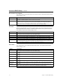
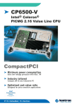
CP6500-V
4-4
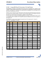
Shorting Chassis GND (Shield) to Logic GND ........................................... 4 - 4
4-5
VGA-CRT Jumper Setting .......................................................................... 4 - 4
4-6
General Purpose LED Setting .................................................................... 4 - 4
4-7
Resistor Setting to Configure COM1 .......................................................... 4 - 5
4-8
Jumper Setting for RS422 RXD Termination (COM1) ................................ 4 - 5
4-10 Resistor Setting to Configure COM2 .......................................................... 4 - 6
4-9
Jumper Setting for RS422 TXD and RS485 Termination (COM1) ............. 4 - 6
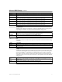
4-11 Jumper Setting for RS422 RXD Termination (COM2) ................................ 4 - 7
4-12 Jumper Setting for RS422 TXD and RS485 Termination (COM2) ............. 4 - 7
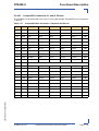
4-14 PCI Interrupt Routing ................................................................................. 4 - 9
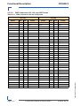
4-15 Memory Map for the 1st Megabyte ............................................................ 4 - 9
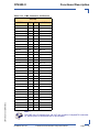
4-16 I/O Address Map ...................................................................................... 4 - 10
4-17 Watchdog Timer Register ........................................................................ 4 - 12
4-18 Geographic Addressing Register ............................................................. 4 - 13
4-19 Watchdog, CompactPCI Interrupt Configuration Register ....................... 4 - 14
4-20 CPCI Master Reset Register .................................................................... 4 - 15
4-21 I/O Status Register ................................................................................... 4 - 16
4-22 Board ID Register .................................................................................... 4 - 16
4-23 Hardware Index Register ........................................................................ 4 - 17
4-24 Hot Swap Control Register ....................................................................... 4 - 17
4-25 Logic Version Register ............................................................................ 4 - 18
4-26 LED Control Register ............................................................................... 4 - 18
4-27 Hot Swap LED Control Register .............................................................. 4 - 19
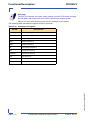
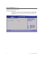
6-1
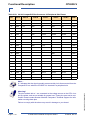
Maximum Input Power Voltage Limits ........................................................ 6 - 3
6-2
DC Operational Input Voltage Ranges ....................................................... 6 - 3
6-3
Input Voltage Characteristics ..................................................................... 6 - 5
6-4
Power Consumption: DOS ......................................................................... 6 - 7
6-5
Power Consumption: Windows® 2000 IDLE Mode .................................... 6 - 7
6-6
Power Consumption: Windows® 2000 100% CPU Usage ........................ 6 - 8
6-7
Power Consumption Table for CP6500-V Accessories .............................. 6 - 8
6-8
Start-Up Current of the CP6500-V ............................................................. 6 - 8
Page x
© 2005 Kontron Modular Computers GmbH
ID 28945, Rev. 01
28945.01.UG.VC.050304/090948
PRELIMINARY
4-13 Interrupt Setting .......................................................................................... 4 - 8