1
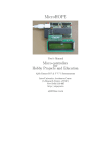
MicroHOPE
User's Manual
Micro-controllers
for
Hobby Projects and Education
Inter-University Accelerator Centre
(A Research Centre of UGC)
New Delhi 110 067
Visit http://expeyes.in/microhope for updates
Chapter 1
Introduction
Most of computer systems in use today are embedded in other machinery, such as automobiles, telephones, appliances, and peripherals for computer systems. Tasks requiring
smaller amounts of processing power and memory are generally implemented using microcontrollers (uC). A micro-controller is a small computer on a single integrated circuit
consisting of a CPU combined with program and data memory, peripherals like analog
to digital converters, timer/counters, serial communication ports and general purpose
Input/Output ports. Intel 8051, Atmel AVR, PIC etc. are popular micro controllers
available in the market. To design the MicroHOPE hardware, we have chosen ATmega32
micro-controller from Atmel AVR series, after considering the hardware resources available on it and the support of Free Software tools like GNU assembler and C compiler.
Why microHOPE ?
Many people who write programs that run on a PC nd it dicult to get started on
coding for a microcontroller, mainly due to:
1. Programming a uC requires some knowledge about the target hardware.
2. Transferring the program from the PC to the target device requires some special
hardware and software.
There are plenty of micro-controller development kits in the market, but most of them
focus on explaining the hardware and software of the development kit rather than the
micro-controller. They teach programming the I/O pins of the development board using
the library functions provided and the user can get things done without understanding
anything about the micro-controller. The objective of this work is to help learning uC
architecture and programming, not the MicroHOPE hardware or software. The focus will
be on the features of the micro-controller without hiding its details from the user.
A simple Graphical User Interface is provided to Edit, Compile (or Assemble) and
upload the program. We start by programming the Input/Output ports of Atmega32,
which require some basic knowledge of binary number system and C language, with its bit
manipulation operators. After that we will proceed to the programming of the peripherals
like ADC, Timer/Counter etc. Since they are more complex, we will start with a software
library, in the form of C source les, that can be included in your program1 . Once you
1 We
are very much aware of the drawback of this method. When you include a le all the functions in
that will get added to your executable, increasing its size. Once the code is working, copy the necessary
functions to your source le, instead of including the whole le, to get rid of this diculty.
2
CHAPTER 1.
INTRODUCTION
3
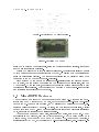
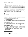
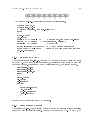
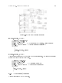
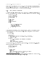
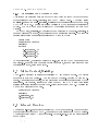
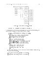
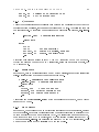
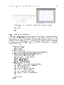
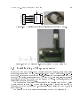
Figure 1.1: (a)MicroHOPE Block diagram.
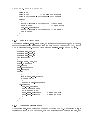
Figure 1.2: MicroHOPE board
learn how to program the peripherals, using the Special Function Registers, there is no
need to use these library functions.
MicroHOPE allows you to code in assembly language. This feature is included mainly
to get a better idea about the architechture of the uC, by playing with the registers and
assembly instructions directly. The content of registers can be displayed using LEDs
connected to the I/O ports of the micro-controller.
Since microHOPE comes with a bootloader pre-installed inside the program memory
of Atmega32, you can upload code using the USB interface with a single click, from the
GUI provided. At the same time, executing the compile and upload programs from a text
terminal are also explained. For compiling the C program we use the avr-gcc compiler
and avrdude for uploading it to the target.
1.1
MicroHOPE Hardware
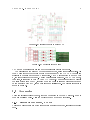
A block diagram of microHOPE hardware is shown in gure 1.1. Programs can be uploaded from the PC through the USB port, with the help of the pre-loaded boot-loader
code on the uC. To load a new program, the PC asserts the RTS signal of MCP2200, generating a pulse that resets ATmega32. On reset, the boot loader code will start, waiting
for new code from the PC. If new code is available it is loaded and control is transferred
to it, otherwise the existing code will start running.
Atmega32 has 32 Input/Output pins, organized as 4 ports, each 8 bit wide. The IC
is available in DIP package, that can be socket mounted. The ATmega32 has 32 kB of
Flash memory, 512 bytes EEPROM and 2 kB Static RAM. Three Timer/Counters, a
serial interface (USART), a byte oriented Two-wire Serial Interface, an 8-channel 10-bit
CHAPTER 1.
INTRODUCTION
4
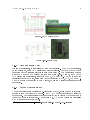
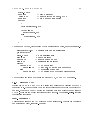
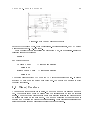
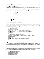
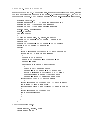
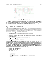
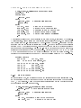
Figure 1.3: Circuit schematic of microHOPE
Figure 1.4: The digital output Board
ADC and an SPI serial port are some of the peripheral devices on the chip.
The processor on the microHOPE board runs at 8MHz, using the external crystal. All
the I/O pins (except the two bits of port D that are used by the UART Rx/Tx pins) are
available to the user on the four I/O connectors. An LED is connected to Bit 0 of Port
B, for quick testing of the board. A reset button is also provided. The 5V USB power,
via a fuse, is connected to both VCC and AVCC inputs. A jumper is provided to disable
the reset option from the PC, required when the board is running programs that need
to communicate with a PC, like a data logger or oscilloscope. The circuit schematic is
shown in gure 1.3
1.2
Accessories
There are several accessory boards, that can be plugged in to the I/O sockets. Some of
them are explained below. Visit the website to know about new additions.
1.2.1 Digital Output Board, 8 LEDs
This can be plugged into any of the four ports to monitor the output, useful for debugging
code.
CHAPTER 1.
INTRODUCTION
5
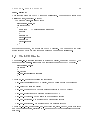
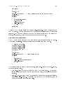
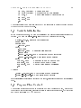
Figure 1.5: LCD display board
Figure 1.6: H-Bridge board
1.2.2 Alphanumeric LCD
For some applications, it is necessary to have a local display. The HD44780 controller,
or compatible IC, based LCD displays are widely available. They come with a 16 pin
connector and the transfer protocol is well documented 2 . The connections between
microHOPE and the LCD display are shown in gure 1.5(a). Pins 4,5 and 7 of the
LCD display are control lines, connected to PC1, PC2 and PC4. The ASCII codes are
transferred in the 4bit mode, using pins 11 to 14 connected to PC4, PC5, PC6 and PC7.
The LCD should be connected to port C socket, to use the C library functions to access
the display.
1.2.3 Motor Control Board
The motor control board consists of 2 H-bridges (IC L293D). Board can be powered from
outside or from the MicroHOPE socket. An INT/EXT jumper is provided to select the
power option. The voltage level at the for outputs of L293 is decided by the four LSBs of
the port on which it is connected. The outputs (A,B,C & D) can be used for controlling
2 DC motors or one stepper motor.
2 For
details refer to http://en.wikipedia.org/wiki/Hitachi_HD44780_LCD_controller
CHAPTER 1.
INTRODUCTION
6
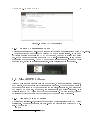
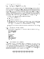
Figure 1.7: MicroHOPE User Interface
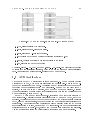
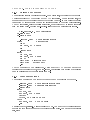
1.2.4 USBASP Programmer board
This is an open sourced ISP (In-System Programming) programmer available from http://www.schl.d
. This is provided as an accessory to MicroHOPE due to several reasons. If you want
to develop programs that uses the UART of Atmega32, you need to upload code using
ISP. It can be used for programming other AVR micro-controllers also. It can be used
for burning the boot loader. The LED on the board indicates power. It goes o while
uploding code, giving an additional indication. More details are given in chapter 4.
1.3
MicroHOPE Software
MicroHOPE's software requirements are a text editor, a cross compiler and assembler,
avr C library, a code uploader and other associated programs. We have written a minimal
text editor (that is our IDE) that can invoke the compiler, uploader etc. and also detect
the MicroHOPE hardware. It can edit, compile/assemble and upload programs. It is
available for both GNU/Linux and MS Windows platforms3 . On MSwindows, you need
to install the Winavr package and the driver for MCP2200 IC from Microchip.
1.3.1 All GNU/Linux Systems
Download and install avr-gcc, avrlib and avrdude from the repositories of your GNU/Linux
distribution. Download the source le uhope.c and the Makele from MicroHOPE website. The command
$ make
3 Download
from http://expeyes.in/microhope
CHAPTER 1.
INTRODUCTION
7
will compile and create the executable uhope, you need to install gtk library. Copy it
to /usr/bin.
$ uhope
will start the program
1.3.1.1
Debian and derivatives, like Ubuntu
Debian package is available on the website. After installing the package, run 'createmicrohope-env' from a terminal to copy the example programs to a directory named
microhope, inside your home directory. The MicroHOPE program can be started from the
applications menu. A screen shot of the microhope IDE is shown in gure 1.7. By default
it looks for les inside a subdirectory named 'microhope', inside your home directory. The
IDE allows you to load/save les, detect the hardware, compile/assemble the code and
upload the output.
The examples given in this document will appear inside the directory named 'microhope'. All les starting with mh- are the les containing library functions to access the
various peripherals of Atmega32. To make the source code visible to the user, they are
not compiled as a library le. Do not modify the les starting with mh-.
You can select any of the example programs, compile/assemble and upload them
using the menu. Correct all the errors before doing Upload. You also need to detect the
hardware once before uploading. For assembly language programs, the le name extension
should be .s or .S (The pre-processor is invoked if .S is used.)
1.3.2 MS Windows
Download and install the software from
http://www.expeyes.herobo.com/microhope.php .
The requirements are the USB to Serial IC drivers, winavr package from
sourceforge.net and the microHOPE installer.
Chapter 2
Getting Started
After installing the required software packages, you must have copied the examples to
a directory named microhope inside your home directory. Start the microHOPE IDE.
Choosing File->Open from the menubar will display all the C les inside the microhope
directory. You can open any of the examples (do not modify the les starting with mh-),
compile/assemble and upload from the IDE. We will start by programming the digital
Input/Output ports of Atmega32, and them proceed to the peripheral devices. 1 .
2.1
Testing the Hardware
Connect MicroHOPE hardware to a USB port and start the microHOPE IDE from the
menu. Click on Detect-MH to get a popup menu of the available USB to Serial devices.
It will contain entries like '/dev/ttyACM0', '/dev/ttyACM1' etc2 . If you are running
expEYES, nd out the device descriptor used by it from the expEYES GUI titlebar and
avoid using the same.
Using File->Open from the menubar, load blink.c from the microhope directory.
Compile and Upload the program by clicking on the menubar. In case of error, check the
USB connections rst. If problem persists, try pressing and releasing the microHOPE
resent button at the same time when you click on Upload. Make sure that the PCRST
jumper is closed.
Once the program is uploaded, the LED connected to PB0 should blink at 1 Hz rate.
If not, press the reset button on the board.
2.2
Input/Output ports of Atmega32
The pinout diagram of Atmega32 is shown in gure 2.1. There are 32 pins organized as
four ports named A, B, C and D, each 8 bit wide. Each pin can be congured as an
input or output. The data direction and transfer are done by writing to the registers
DDRX, PORTX and PINX (where X stands for A, B, C or D). The avr-gcc compiler
allows us to program the registers and their individual bits using the same names given
in the Atmega32 manual. The C compiler allows you to access them just like normal
variables. For example, the statement PORTB = 15 , writes the number 15 to Port B.
The individual pins are referred using names like PA0, means BIT 0 of Port A.
1 For
2 For
complete details of Atmega32 refer to http://www.atmel.in/Images/doc2503.pdf
old model of microHOPE using FT232, it will be ttyUSB*
8
CHAPTER 2.
GETTING STARTED
9
Figure 2.1: Atmega32 Pinout
• DDRX : Direction of every pin of an I/O port is decided by the state of corresponding
bit in the Data Direction registers DDRX. To congure a pin as output, make the
bit 1, and to make it as input make it zero. For example, DDRA = 1 will congure
BIT 0 of Port A (PA0) as output, and all other pins as input.
• PORTX : For pins that are congured as ouput, assigning a value to PORTX will
set that data on them. For example PORTA = 1 will make PA0 high, that can be
measured on the pin number 40 of the IC.
• PINX : For the pins congured as inputs, PINX will read the status of the external
voltage level connected to the pins. For pins that are congured as outputs, PINX
will return the data written to PORTX.
If the pins congured as inputs are left unconnected, there could be unwanted level changes
due to electrical noise, this can be prevented by enabling the internal pull-up resistor. For
pins that are congured as inputs, setting/clearing the bits in PORTX will enable/disable
the corresponding internal pullup resistor.
The operations described above can be understood easily with some examples. For a
quick test, MicroHOPE hardware has an LED connected to PB0, with a series resistor
for current limiting.
2.2.1 Reading and Writing Ports
The program copy.c reads the voltage level at PA0 (Pin 0 of Port A) and sets the same
on PB0, where we have the LED. We will enable the internal pullup resistor on PA0 so
that and it will go LOW only when it is connected to ground using a piece of wire.
#include <avr/io.h>
int main (void)
{
DDRA = 0;
PORTA = 1;
DDRB = 1;
for(;;)
// Include file for I/O operations
// Port A as Input
// Enable pullup on PA0
// Configure PB0 as output
CHAPTER 2.
}
GETTING STARTED
PORTB = PINA;
10
// Read Port A and write it to Port B
To test this example, open copy.c from the File menu of microHOPE IDE, Click on
Compile and then Upload from the menubar The LED on PB0 should start glowing after
uploading the program. LED will be o when you connect PA0 to ground. You may
rewrite the program so that the LED may be controlled by some other bit congured as
input.
The simple program given above has certain drawbacks. It changes PORTB as a
whole instead of acting on PB0 alone. Suppose we have something else connected to the
other pins of Port B, they also will be aected by the action of P ORT B = P IN A. To
avoid such problems, we should manipulate individual bits. The include le mh-digital.c
contains macros for setting and clearing bits by specifying their position.
2.2.2 Bit manipulation macros3
These macros can be used on variables, dened in the program, and also on registers like
DDRX, PORTX etc.
BITVAL(bit position)
The value of bit position could be 0 to 7 in the case of 8 bit integers and 0 to 15 for 16
bit integers. This macro returns (1 << bit position). For example BITVAL(3), will give
8, that is binary 1000, obtained by left shifting of 1 thrice.
SETBIT(variable, bit position)
This macro SETS the specied bit in the given variable, without aecting the other bits.
For example SETBIT(DDRB, 7), will make the last bit of DDRB high.
CLRBIT(variable, bit position)
This macro clears the specied bit of the given variable. For example CLRBIT(val, 0),
clears the least signicant bit of 'val', that is an integer type variable.
GETBIT(variable, bit position)
This macro returns the value the specied bit if the specied bit of the variable is 1, else
it returns zero. For example: if x = 3, GETBIT(x, 1) will return 2 and GETBIT(x,3)
will return zero.
Let us rewrite the previous program as copy2.c, using these macros as:
#include <avr/io.h>
int main (void)
{
3 The
macros are implemented using:
#dene BITVAL(bit) (1 << (bit))
#dene CLRBIT(sfr, bit) (_SFR_BYTE(sfr) &= ~BITVAL(bit))
#dene SETBIT(sfr, bit) (_SFR_BYTE(sfr) |= BITVAL(bit))
#dene GETBIT(sfr, bit) (_SFR_BYTE(sfr) & BITVAL(bit))
CHAPTER 2.
GETTING STARTED
uint8_t val;
DDRA = 0;
PORTA = 1;
DDRB = 1;
for(;;)
11
// Port A as Input
// Enable pullup on PORTA, bit 0
// Pin 0 of Port B as output
{
val = GETBIT(PORTA, 0);
if (val != 0)
SETBIT(PORTB, 0);
else
CLRBIT(PORTB, 0);
}
}
The same can be done, without using the bit manipulation macros, as shown in copy3.c
#include <avr/io.h>
int main (void)
{
uint8_t val;
DDRA = 0;
PORTA = 1;
DDRB = 1;
for(;;)
}
if(PINA & 1)
PORTB |= 1;
else
PORTB &= ~1;
// Include file for I/O operations
// 8 bit unsigned word
// Port A as Input
// Enable pullup on PA0
// Configure PB0 as output
//
//
//
//
If PA0 is set
Set PB0, by ORing with 00000001b
otherwise clear PB0
by ANDing with 11111110b (~00000001b)
The code fragment shown above uses the Bitwise AND, OR and NOT operators.
2.2.3 Blinking LED
Making pin PB0 HIGH and LOW in a closed loop result in the blinking of the LED
conencted to it. We need to slow down the rate of blinking so that it can be perceived by
our eyes. This can be done by making the processor wait for a while between writing to
PORTB. There are some delay functions provided for this. The le mh-utils.c contains
the following functions:
delay_100us(int n)
This function will make the CPU idle for n x100 microseconds. For example to insert a
200 microsecond delay, call delay_100us(2)
CHAPTER 2.
GETTING STARTED
12
delay_ms(int n)
This function will make the CPU idle for n milliseconds. For example to insert a 500
millisecond delay, call delay_ms(500)
The program blink.c lis listed below:
#include mh-utils.c
int main (void)
{
DDRB = 1;
// configure PB0 as output
for(;;)
{
PORTB = 1;
delay_ms(500);
PORTB = 0;
delay_ms(500);
}
}
If everything goes ne, you should see the LED blinking. You can remove the delay
statements and watch the high frequency pulses on PB0 using an oscilloscope.
2.3
The LCD Display
The le mh-lcd.c contains functions to access the display, connected to port C. The
example program hello.c listed below demonstrates the usage of the LCD display.
#include "mh-lcd.c"
int main()
{
lcd_init();
lcd_put_string("Hello World");
}
The le mh-lcd.c provides the following functions :
• lcd_init() : Initializes the LCD display, must be called once in the beginning
• lcd_clear() : Clears the display
• lcd_put_char(char ch) : Outputs a single character to the LCD display
• lcd_put_string(char* s) : Displays a string to the LCD
• lcd_put_byte(uint8_t i) : Diplays an 8 bit unsigned integer
• lcd_put_int(uint16_t i) : Displays a 16 bit unsigned integer
• lcd_put_long(uint32_t i) : Displays a 32 bit unsigned integer
The le mh-lcd-oat.c provides lcd_put_oat(oat val, uint8_t ndec), where ndec is the
number of decimal places, restricted to 3. Dening oat type data increases the program
size a lot.
CHAPTER 2.
2.4
GETTING STARTED
13
Analog to Digital Converter
Most of the I/O PORT pins of Atmega32 have alternate functions. PA0 to PA7 can be
used as ADC inputs by enabling the built-in ADC. All the pins congured as inputs in the
DDRA will become ADC inputs, but the ones congured as outputs will remain as digital
output pins. The ADC converts the analog input voltage in to a 10-bit number. The
minimum value represents GND and the maximum value represents the ADC reference
voltage. The reference inputs could be AVCC, an internal 2.56V or a voltage connected
to the AREF pin. The selection is done in software. The ADC operation is controlled via
the registers ADMUX and ADCSRA. The data is read from ADCH and ADCL.
The include le 'mh-adc.c' provides the following functions:
1. adc_enable() : Enables the ADC
2. adc_disable() : Disables the ADC
3. adc_set_ref(ref) : Select the reference, where ref is REF_EXT is an external voltage is applied to the AVREF pin, REF_INT to use the internal 2.56 V reference
and REF_AVCC to connect the AVCC supply internally to AVREF.
4. read_adc(ch) : Converts the voltage on channel ch and returns it in a 16 bit number.
2.4.1 Reading an Analog Voltage
The example program
adc.c
, reads an ADC input and display the result on the LCD.
#include "mh-lcd.c"
#include "mh-adc.c"
main()
{
uint16_t data;
lcd_init();
adc_enable();
data = read_adc(0);
lcd_put_int(data);
}
2.4.2 Programmig ADC registers
The operation of the ADC is controlled mainly by the registers ADCSRA and ADMUX.
Setting ADEN will enable the ADC and setting ADSC will start a conversion. The bit
ADIF is set after a conversion and this bit can be cleared by writing a '1' to it. The
ADSP bits decide the speed of operation of the ADC, by pre-scaling the clock input. The
channel number is selected by the MUX0 to MUX4 bits in the ADMUX rregister. The
reference input is selected by the REFS0 and REFS1 bits.
CHAPTER 2.
GETTING STARTED
14
The program adc-v2.c, demonstrates the usage of these registers.
#include <avr/io.h>
#include "mh-lcd.c"
// convert channel 0, set pre-scaler to 7
main()
{
uint16_t data;
lcd_init();
ADCSRA = (1 << ADEN) | 7;
// Enable ADC, set clock pre-scaler
ADMUX = (1 << REFS0);
// AVCC reference, channel 0
ADCSRA |= (1 <<ADSC);
// Start ADC
while ( !(ADCSRA & (1<<ADIF)) ) ; // wait for ADC conversion
data = (ADCH << 8) | ADCL;
// make 10 bit data from ADCL and ADCH
lcd_put_int(data);
}
2.4.3 Reading in a Loop
The example program adc-loop.c , reads an ADC input in a loop and display the result
on the LCD. If the input is left unconnected, the displayed value could be anywhere
between 0 an 1023. Connecting PA0 to 5V will display 1023, the maximum output.
#include "mh-lcd.c"
#include "mh-adc.c"
#include "mh-utils.c"
main()
{
uint16_t data;
lcd_init();
adc_enable();
for (;;)
{
data = read_adc(0);
lcd_clear();
lcd_put_int(data);
}
delay_ms(100);
}
Modify the code for reading other ADC channels.
2.4.4 Temperature Control
The program adc-loop.c can be easily modied to make a temperature monitor/controller
using the LM35 temperature sensor. Connect LM35 output to PA0. At 1000 C , the
CHAPTER 2.
GETTING STARTED
15
Figure 2.2: 8 bit Timer/Counter0 Schematic
output of LM35 will be 1 volt. With the internal 2.56 volts as reference, the ADC output
will be around 400 (1.0 / 2.56 * 1023).
Drive the relay contact controlling the heater from PB0, via a transistor. Insert the
following line in the beginning
DDRB = 1
and within the loop:
if (data > 400)
// switch off heater
PORTB = 0;
else if (data < 395)
// switch on heater
PORTB = 1;
The heater will be switched OFF when the ADC output is greater than 400. It will be
switched ON only when the output goes below 395. The window of 6 is given to avoid
the relay chattering.
2.5
Timer/Counters
ATmega16 has three counter/timer units. Two of them are of 8 bit size and one is 16
bit. The counter input could be derived from the internal clock or from an external
source. The output of the counter is compared with setpoint registers and dierent types
of actions are taken on compare match. The mode of operation of Counter/Timer is
programmed by setting the bits in the control registers. These circuits are useful for time
interval measurements and generating dierent kinds of waveforms.
CHAPTER 2.
GETTING STARTED
16
2.5.1 8 bit Timer/Counter0
A block diagram of Timer/Counter0 is shown in gure2.2. The counter TCNT0 gets its
input and control signals from the control logic circuit. The counter output is compared
with a Output Compare Register OCR0 and a compare match can trigger dierent types
of actions, like generating a waveform on OC0 (pin 4 of Atmega32, same as PB3). The
mode of operation is decided by the register TCCR0, shown below:
Let us start using Timer/Counter0 with the help of the following functions.
sqwave_tc0(csb, ocrval)
This function generates a square wave on OC0, whose frequency is decided by the clock
select bits (csb) and ocrval. Example sqwave-tc0.c listed below demonstrates the usage
of this function.
// example : sqwave-tc0.c
#include "mh-timer.c"
csb = 2;
// Clock select bits
ocrval = 99; // Output Compare register vaule
int main()
{
sqwave_tc0(csb, ocrval);
}
The 8MHz system clock is divided by 8 (csb =2, refer to table below) to get a 1MHz input
to the counter. The OCR0 register is set to 99. The mode bits are set such that the when
the counter value reaches the OCR0, the output is toggled and counter is cleared. This
will result in the waveform generator output toggles after every 100 clock cycles, giving a
5kHz sqaurewave on pin OC0 (PB3). You may view this on an oscilloscope. If you do not
have one, connect a loudspeaker with a 100Ω series resistor from PB3 to ground. We have
used expEYES for viewing and characterizing the waveforms generated by microHOPE.
Changing ocrval to 199 will give output 2.5kHz on the output. The output frequency
is given by the relation
fclock
f=
2.N.(1 + OCR0)
where fclock is the system clock and N is the clock division factor, as shown below.
CHAPTER 2.
GETTING STARTED
17
pwm_tc0(csb, ocrval)
This function generates a Pulse Width Modulated waveform on OC0, whose frequency is
decided by the clock select bits (csb) and the duty cycle by the ocrval. The output OC0
is cleared when the counter reaches the OCR0 value, the counter proceeds upto 255 and
then sets OC0. The program pwm-tc0.c generates a 3.9 kHz PWM with 25% dutycycle.
// example : pwm-tc0.c
#include "mh-timer.c"
uint8_t csb = 2; // Clock select bits uint8_t
ocrval = 63;
// Output Compare register vaule
int main()
{
pwm_tc0(csb, ocrval);
}
PWM waveforms are often used for generating analog DC voltages, in 0 to 5 volts range,
by ltering it using an RC circuit. It is better to set a higher frequency so that the lter
RC value could be small. The frequency can be made 31.25kHz by setting csb=1. The
DC level is decided by the value of OCR0, ranging from 0 to 255. Once you learn howto
manipulate the control registers, the same thing can be done without calling the library
function, as shown below.
// example : pwm-tc0-v2.c
#include <avr/io.h>
uint8_t csb = 1;
// Clock select bits uint8_t
ocrval = 254/4;
// Output Compare register vaule
int main()
{
// Set TCCR0 in the Fast PWM mode
TCCR0 =(1 << WGM01) | (1 << WGM00) | (1 << COM01) | csb;
OCR0 = ocrval;
TCNT0 = 0;
DDRB |= (1 << PB3); // Set PB3(OC0) as output
}
Connect a 1k resistor and 100uF capacitor in series from PB3 to ground,as shown below,
and measure the voltage across the capacitor using a voltmeter.
2.5.2 16 bit Timer/Counter1
The Timer/Counter1 has more features like two Output Compare Registers, Input Capture unit etc., as shown in gure2.3. The frequency and duty cycle of the waveforms can
be controlled better due to the 16 bit size of the counters. Some C functions to use the
T/C1 are given below.
CHAPTER 2.
GETTING STARTED
18
Figure 2.3: 16 bit Timer/Counter1 schematic
sqwave_tc1(csb, OCRA)
// example : sqwave-tc1.c
#include "mh-timer.c"
uint8_t csb = 2;
// 2 is divide by 8 option, 1MHz clock in
uint16_t ocra = 50000; // Output Compare register A
int main()
{
sqwave_tc1(csb, ocra);
}
pwm10_tc1(csb, OCRA)
This function generates a PWM waveform with 10bit resolution. The value of ocra should
be from 0 to 1023 to set the duty cycle.
// example : pwm-tc1.c
#include "mh-timer.c"
uint8_t csb = 1;
// 1 => 8MHz clock in
uint16_t ocra = 1024/3; // Duty cycle arounf 33%
int main()
{
pwm10_tc1(csb, ocra);
}
2.5.3 8 bit Timer/Counter2
This one is similar to Timer/Counter0.
CHAPTER 2.
GETTING STARTED
19
sqwave_tc2(uint32_t freq)
This function generates a square wave on OC2. The clock selction bits and the OCR2
value are calculated. It is not possible to set all frequency values using this method. The
actual frequency set is returned and displayed on the LCD.
//Example sqwave-tc2.c
#include "mh-timer.c"
#include "mh-lcd.c"
int main()
{
uint32_t f;
lcd_init();
f = set_sqr_tc2(1500);
lcd_put_long(f);
}
PWM by programming the registers
The example given below demonstrates the usage of T/C2 as a PWM waveform generator,
by setting the control register bits. The duty cycle is set to 25% by setting the OCR2 to
one fourth of the maximum.
// example : pwm-tc2.c
#include <avr/io.h>
uint8_t csb = 2;
// Clock select bits uint8_t
ocrval = 255/4;
// Output Compare register vaule
int main()
{
// Set TCCR2 in the Fast PWM mode
TCCR2 =(1 << WGM21) | (1 << WGM20) | (1 << COM21) | csb;
OCR2 = ocrval;
TCNT0 = 0;
DDRD |= (1 << PD7); // Set PD7(OC2) as output
}
2.5.4 More applications of Timer/Counter
Timer/Counter can be used for timing applications, like measuring the time elapsed between two events or counting the number of pulse inputs during a specied time interval.
measure_frequency()
This function counts the number of pulses received on the external input of Timer/Counter1
(PB1) during 500 milliseconds to calculates the frequency of the input pulse.
// Example freq-counter.c
#include "mh-utils.c"
#include "mh-timer.c"
#include "mh-lcd.c"
CHAPTER 2.
GETTING STARTED
20
int main()
{
uint32_t f;
set_sqr_tc2(1500);
// Set a square wave on TC2 output (PD7)
lcd_init();
while(1)
{
f = measure_freq();
lcd_clear();
lcd_put_long(f);
delay_ms(200);
}
return 0;
}
Connect PD7 to PB1 and upload the program freq-counter.c to read the frequency on
the LCD display. You can also connect PB1 to an external pulse source to measure its
frequency. The maximum frequency that can be measured is limited by the size of the
counter, that is 63535, means we it can handle upto around 126 kHz.
Time Interval Measurement
The T/C units can be programmed to keep track of time interval between two events.
The program r2ftime.c measures the rising edge to falling edge time on PB1.
// Example r2ftime.c
#include "mh-utils.c"
#include "mh-timer.c"
#include "mh-lcd.c"
int main()
{
lcd_init();
set_sqr_tc2(500);
// Test signal on PD7
while(1)
{
lcd_clear();
lcd_put_long(r2ftime(PB1));
delay_ms(100);
}
}
The function r2ftime() uses two other functions, called start_timer() and read_timer(),
that are explained below.
• void start_timer() : Start the counter with a 1 MHz clock input. An interrupt
service routine is activated when the count reached 50000, that increments another
interger.
• uint32_t read_timer() : Stops the counter and returns the microseconds elapsed
after calling start_timer(). There will be an error of 2 to 3 microseconds, that is
due to the overhead of the function calls.
CHAPTER 2.
2.5.4.1
GETTING STARTED
21
Distance Measurement
This technique is used for measuring distance using an ultrasound echo module HYSRF054 , using ultra-sound-echo.c. The trigger is connected to PB0 and the echo is
connected to PB1. The distance is measured by
// Example ultra-sound-echo.c
#include "mh-utils.c"
#include "mh-timer.c"
#include "mh-lcd.c"
int vsby2 = 17; // velocity of sound in air = 34 mS/cm
int main()
{
uint32_t x;
DDRB |= (1 << PB0); // set PB0 as output
DDRB &= ~(1 << PB1); // and PB1 as inpt
lcd_init();
while(1)
{
PORTB |= (1 << PB0);
// set PB0 HIGH
delay_100us(1);
PORTB &= ~(1 << PB0); // set PB0 LOW
delay_100us(5);
// Wait for a while to avoid false triggering
start_timer();
while( (PINB & 2) != 0 ) ;
// Wait for LOW on PB1
x = read_timer() + 400;
lcd_clear();
lcd_put_long(x*vsby2/1000); // distance in cm
delay_ms(500);
}
}
2.6
Talking to the PC, via USB
On the microHOPE board, the Rx/Tx pins of ATmega32 are connected to the USB to
Serial Converter IC. User programs also can use this path to communicate to the PC via
the USB port.
The following functions are available for handling the UART
1. uart_init(baud) : 38400 is the maximum baudrate supported. You can use any
submultiple of that. We use 1 Stop Bit and the parity is Even.
2. uart_recv_byte() : Waits on the UART receiver for a character and returns it
3. uart_send_byte(c) : Sends one character over the UART transmitter.
On the PC side, we use a simple Python program to communicate to the micro-controller.
The USB to Serial interface will appear as a virtual COM port on the PC, on GNU/Linux
4 http://www.robot-electronics.co.uk/htm/srf05tech.htm
CHAPTER 2.
GETTING STARTED
22
systems it can be accessed as /dev/ttyACM0. You need to install Python interpreter and
the python-serial module on the PC for this to work. These Python programs should be
terminated before using MicroHOPE again to upload programs.
2.6.1 Send/receive Characters
The program echo.c waits for data from the PC, vis the USB to serial converter, increment
it by one and sends it back. The received data is also displayed on the local LCD display.
#include "mh-lcd.c"
#include "mh-uart.c"
int main(void)
{
uint8_t data;
lcd_init();
uart_init(38400);
for(;;)
{
data = uart_recv_byte();
lcd_put_char(data);
uart_send_byte(data);
}
}
After uploading this program, open a terminal window, change to the directory named
microhope and run the python program echo.py listed below, using the commands:5
$ cd microhope
$ python echo.py
import serial
fd = serial.Serial('/dev/ttyACM0', 38400, stopbits=1, \
timeout = 1.0)
while 1:
c = raw_input('Enter the character to send: ')
fd.write(c)
print 'Receiced ', fd.read()
We can rewrite echo.c without using the library functions. The program echo-v2.c listed
below id functionally identical to echo.c
#include "mh-lcd.c"
int main(void)
{
uint8_t data;
lcd_init();
//38400 baudrate, 8 databit, 1 stopbit, No parity
UCSRB = (1 << RXEN) | (1 << TXEN);
5 If
you are using old microHOPE with FT232 IC, edit echo.py to replace ttyACM0 with ttyUSB0.
The same thing applies to programs like cro.py, pymicro.py etc.
CHAPTER 2.
}
GETTING STARTED
23
UBRRH = 0;
UBRRL = 12;
// At 8MHz (12 =>38400)
UCSRC = (1<<URSEL) | (1<<UCSZ1) | (1<< UCSZ0);
for(;;)
{
while ( !(UCSRA & (1<<RXC)) ); //wait on Rx
data = UDR;
// read a byte
lcd_put_char(data);
while ( !(UCSRA & (1<<UDRE)) ); // Rx Empty ?
UDR = data;
}
2.6.2 Sending ADC data
The program remote-adc.c, listed below, on receiving a channel number, in 0 to 7 range,
reads the corresponding channel and send the data to the PC using the UART, via the
USB to Serial converter. Use the Python program remote-adc.py on the PC side.
#include "mh-lcd.c"
#include "mh-uart.c"
#include "mh-adc.c"
int main(void)
{
uint8_t chan, low, hi;
uint16_t adcval;
lcd_init();
uart_init(38400);
adc_enable();
for(;;)
{
data = uart_recv_byte();
if (chan <= 7)
{
adcval = read_adc(chan);
lcd_clear();
lcd_put_int(low);
low = adcval & 255;
hi = adcval >> 8;
uart_send_byte(low);
// send LOW byte
uart_send_byte(hi);
// send HI byte
}
}
}
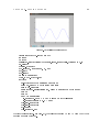
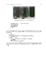
2.6.3 A simple Oscilloscope
The program cro.c can waits for a command byte from the PC. On receiving a '1', it
digitizes the input at PA0 500 times, with 100 microseconds in between samples, and
CHAPTER 2.
GETTING STARTED
24
sends the data to the PC. The program cro.py sends the necessary command, receives
the data and displays it as shown in the gure2.4. While running cro.py , the PCRST
jumper should be open. The C program running on the micro-controller is listed below.
#include <avr/io.h>
#define READBLOCK 1
// code for readblock is 1
#define NS 500 // upto1800 for ATmega32
#define TG 100 // 100 usec between samples
uint8_t tmp8, dbuffer[NS];
uint16_t tmp16;
int main (void)
{
// UART at 38400 baud, 8, 1stop, No parity
UCSRB = (1 << RXEN) | (1 << TXEN); UBRRH = 0;
UBRRL = 12;
UCSRC = (1 <<URSEL) | (1 << UCSZ1) | (1 << UCSZ0);
ADCSRA = (1 << ADEN); // Enable ADC
for(;;)
{
while ( !(UCSRA & (1<<RXC)) ); // wait for the PC
if(UDR == 1) // '1' is our command
{
TCCR1B = (1 << CS11);
ADMUX = (1 << REFS0) |(1 << ADLAR) | 0;
ADCSRA |= ADIF;
for(tmp16 = 0; tmp16 < NS; ++tmp16)
{
TCNT1 = 1; // counter for TG
ADCSRA |= (1 << ADSC) | 1; // Start ADC
while ( !(ADCSRA & (1<<ADIF)) ) ; // Done ?
dbuffer[tmp16] = ADCH; // Collect Data
ADCSRA |= ADIF; // reset ADC DONE flag
while(TCNT1L < TG) ; // Wait TG usecs
}
while( !(UCSRA & (1 <<UDRE) ) ); // Wait Tx empty
UDR = 'D'; // Send a 'D' first
for(tmp16=0; tmp16 < NS; ++tmp16) // Send to the PC
{
while( !(UCSRA & (1 <<UDRE) ) );
UDR = dbuffer[tmp16];
}
}
}
}
The Python program cro.py
import serial, struct, time
import numpy as np
CHAPTER 2.
GETTING STARTED
25
Figure 2.4: Oscilloscope screen shot
import matplotlib.pyplot as plt
NP = 500
TG = 100
fd=serial.Serial('/dev/ttyACM0',38400,stopbits=1,timeout = 1.0)
fd.flush()
fig=plt.figure()
plt.axis([0, NP*TG/1000, 0, 5])
plt.ion()
plt.show()
va =ta = range(NP)
line, = plt.plot(ta,va)
while 1:
fd.write(chr(1)) # command for the uC
print fd.read() # This must be a 'D'
data = fd.read(NP)
raw = struct.unpack('B'* NP, data) # convert to byte array
ta = []
va = []
for i in range(NP):
ta.append(0.001 * i * TG) # micro to milliseconds
va.append(raw[i] * 5.0 / 255)
line.set_xdata(ta)
line.set_ydata(va)
plt.draw()
time.sleep(0.05)
Modifed versions (cro2.c and cro2.py), that allows changing NS and TG from the Python
program are also provided.
CHAPTER 2.
GETTING STARTED
26
2.6.4 Controlling the uC from Python
This section demonstrates a simple method to read/write the Input/Output ports and
other registers of the micro-controller, from the PC using Python. A program called
pymicro.c runs on the micro-controller. It listens over the serial port for two commands,
READB or WRITEB. The rst one should be followed by the address of the register to
be read. The WRITE command is followed by the register address and the data to be
written.
On the PC side, pymicro.py handles the communication to the micro-controller. It
denes a class named atm32, that contains the communication routines. The example
program listed below demonstrates a blinking LED code in Python
import time
from pymicro import *
u=atm32()
while 1:
u.outb(PORTB, 1)
time.sleep(0.5)
u.outb(PORTB, 0)
time.sleep(0.5)
To run this program, compile and upload pymicro.c, remove the PCRST jumper and then
run blink.py. It is very easy to implement some programs, for example a stepper motor
controller in Python, using this method.
2.7
Motor Control, H-bridge
The H-bridge accessory is useful for controlling DC and stepper motors. The circuit
schematic is shown in gure2.5. One can use the pymicro.c program to test the Hbridge. After uploading pymicro, you can control the motor control outputs from Python
interpreter. For example, connect the board to port A and a DC motor (with series
resistor for current limiting) between the H-bridge output pins A and B. The following
Python code will rotate the motor.
from pymicro import *
p=atm32()
p.outb(DDRA,15)
p.outb(PORTA,1)
2.8
Infrared Receiver
The program ir-recv.c can receive data using the TSOP1738 IR receiver. The output of the
chip is connected to bit 2 of PORTD. The received byte is displayed on the LCD display.
The receiver tested using TV remote controls. To test ir-recv.c, make the connections as
shown below:
CHAPTER 2.
GETTING STARTED
27
Figure 2.5: H-bridge schematic
Press some buttons on the remote control panel. The received number will be displayed
on the LCD display of microHOPE. The code ir-recv.c is available on the website. It can
be modied to work with the single byte IR transmitted from expEYES.
2.9
Alternate Serial Port
The Atmega32 controller has only one Serial Port (UART), that is already connected to
the USB to Serial converter. In order to communicate to other devices that supports
serial communication, we have a simple library that will convert PD2 to a Transmit pin
and PD3 a Receive pin. The functions available are:
• enable_uart(9600) // baudrates 2400,4800, 9600 & 19200 only
• uart_read() , returns one byte from the receiver buer, call only when variable
ubcount is nonzero
• uart_write(uint8_t) , writes a byte to the transmitter
• disable_uart() , disable the interrupts
The Soft Serial code is tested by connecting PD2 (soft Rx) and PD3 (soft Tx) to a
computer through the USB to Serial converter MCP2200 (by using another microHOPE
board with the uC removed). The Transmit output from MCP2200 that appears on pin
14 of the uC socket is connected to PD2. Receive input (on pin15) is connected to PD3.
The program soft-echo.c, listed below, waits for data from the PC and the received data
is send to the LCD display and also to the PC via PD3.
#include "mh-soft-uart.c"
#include "mh-lcd.c"
int main()
{
uint8_t x=0;
lcd_init();
enable_uart(9600); // 2400,4800, 9600 & 19200 allowed
for(;;)
CHAPTER 2.
GETTING STARTED
28
Figure 2.6: Connection to PC via soft serial port
{
}
while(!ubcount) ; // wait for Rx data
x = uart_read();
lcd_put_char(x);
uart_write(x);
}
The Python echo.py is used on the PC side. The device name is shown as /dev/ttyACM1,
assuming that /dev/ttyACM0 is already taken by the microhope board used for program
development.
import serial
fd = serial.Serial('/dev/ttyACM1', 9600, stopbits=1, \
timeout = 1.0)
while 1:
c = raw_input('Enter the character to send: ')
fd.write(c)
print 'Receiced ', fd.read()
Even though this code has been tested, it seems to be having severe limitations. Receiver
cannot handle data coming a high rates, require at least 2 to 3 milliseconds gap between
bytes.
Chapter 3
Coding in Assembly Language
Main objective of this chapter is to learn the architecture of the micro-controller rather
than developing large programs. Some examples justifying coding in assembly for better
performance will be demonstrated. One concern with assembly or machine language coding is that the work is specic to the architecture of the selected device. The approach will
be to examine the architecture in a generic manner and provide some example programs
that are more or less common to any kind of processors.1
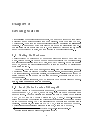
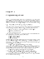
Major components of a micro-controller are shown in gure3.1. After powering up (or
Reset) the Program Counter in initialized to zero, so that it points to the beginning of the
Program Memory. The instruction stored at that location is brought to the Instruction
Decoder and executed. This could be operations like; moving data between the Working
Registers and RAM, performing some arithmetic and logical operations, changing the
content of the program counter, etc. Writing to the Special Function Registers control the
Input/Output pins and also the operation of peripheral devices like ADC, Timer/Counter
etc. The popular family of micro-controllers like 8051, AVR and PIC follows the same
architechture, even though the details may dier. Understanding them from a generic
point of view makes switching from one type of device to another easier.
To program in assembly language, we need to have some understanding about the
Instruction Set, the Registers and the memory conguration of the micro-controller. We
also need to know the syntax supported by the assembler we use, there is usually small
dierences between various assemblers. Since we are using Atmega32, belonging to the
AVR family, and the GNU assember for AVR, further discussions will be restricted to
them.
3.1
Format of an Assembler Program
A single line of code may have a
• Label: , always terminated by a colon
• The instruction
• The operands (could be 0, 1 or 2 of them)
• A comment starting with a semicolon
1 http://sourceware.org/binutils/docs/as/
29
CHAPTER 3.
CODING IN ASSEMBLY LANGUAGE
30
Figure 3.1: A block diagram of Micro-controller
lab1: INC R1
;increment the content of Register r1
The instruction and operand is not case sensitive but the labels are case sensitive, Lab1
is not the same as lab1. A complete program is shown below.
;first.s , example assembler program, for avr-gcc.
work = 1
.equ DDRB, 0x37 ; memory mapped addresses
.equ PORTB, 0x38 ; of DDRB and PORTB
.section .data ; the data section
var1:
.byte 15 ; global variable var1
.section .text ; The code section
.global __do_copy_data ; initialize variables
.global __do_clear_bss ; and setup stack
.global main ; declare label main as global
main:
lds work, var1 ; load var1 to R1
sts DDRB, work ; PB0 as output
sts PORTB, work ; set PB0 HIGH
.end
1. The Working registers (R1 to R31) and the SFRs can be assigned dierent names,
as shown in the beginning.
2. .data, starts a data section, initialized RAM variables.
3. .text, starts a text section, code and ROM constants.
CHAPTER 3.
CODING IN ASSEMBLY LANGUAGE
31
Figure 3.2: AVR memory maps.(a)Data memory.(b) Program memory
4. .byte, allocates single byte constants.
5. .ascii, allocates a non-terminated string.
6. .asciz, allocates a \0-terminated string.
7. .set declares a symbol as a constant expression (identical to .equ)
8. .global, declares a public symbol that is visible to the linker
9. .end, singies the end of the program
The lines .global __do_copy_data and .global __do_clear_bss will tell the compiler
to insert code for initializing variables, which is a must for programs having initialized
data. Assembling and uploading rst.s will set the 4 LSBs of port B.
3.2
AVR Architecture
A schematic of the AVR architecture is shown in gure 3.1. The 32 General Purpose
Registers (R1 to R31, 8 bit wide) are also called the Register File. Data is moved between the Registers and the memory. Addressing memory locations above 255 is done by
combining two 8bit registers to form a 16 bit register. R26 and R27 combined is the X
register, R28 with R29 is the Y register, and R30 with R31 is the Z register. Dierent
types of addressing modes are dened for transferring data between the Registers and the
memory locations, mostly the SRAM.
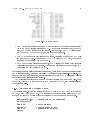
In the AVR data memory space (gure 3.2), locations 0 to 31 (0x1F)are occupied by
the Register File. Generally the assembler refers to them by names R1 to R31, not by the
adresses. Location 0x20 to 0x5F (32 to 95) are occupied by the Special Function Registers
(SFR), like the Status Register, the Stack Pointer and the control/status registers of the
peripherals. The Special Function Registers can also be accessed using the I/O address
space ranging from 0 to 0x3F, using IN and OUT insructions. Some of the special function
registers are shown in gure 3.3(b), refer to the Atmega32 data sheet for a complete list.
Use the address given inside the parantheses to access them as memory locations.
CHAPTER 3.
CODING IN ASSEMBLY LANGUAGE
32
The rst Register is SREG, the status register that holds the ags resulting from
the last executed arithmetic or logical instruction. There are several instructions whose
results depend on the status of the bits inside SREG. Availability of SREG as a special
function register allows us to examine the status of various ags, after arithmetic and
logical operations. Stack Pointer is used as a pointer to the data address space. PUSH
and POP instructions are used for moving data between the register le and location
specied by the stack pointer.
All the peripherals and the general purpose I/O ports are operated by accessing the
corresponding SFRs. We will be using ports A and B to view data written to them using
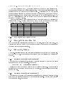
8 LEDs. The SFRs used often in the example programs are listed below.
Name
I/O Addr. Mem Addr
Function
DDRA
0x1A
0x3A
Data Direction of Port A
PORTA
0x1B
0x3B
Output to Port A
PINA
0x19
0x39
Input from Port A
DDRB
0x17
0x37
Data Direction of Port B
PORTB
0x18
0x38
Output to Port B
PINB
0x16
0x36
Input from Port B
SREG
0x3F
0x5F
Status Register
3.2.1 The Program Memory Space
3.3
Atmega32 Instruction Set
For a complete list of instructions supported by Atmega32, refer to the data sheet. We
will only examine some of them to demonstrate dierent types of memory addressing and
the arithmetic and logical operations.
3.4
Addressing Modes
The micro-controller spends most of the time transferring data between the Register File,
SFRs and the RAM. Let us examine the dierent modes of addressing the Registers and
Memory.
3.4.1 Register Direct (Single Register)
The contents of the register is read, specied operation is performed on it and the result
is written back to the same register. For example
Lab1:
INC
R2
; increments Register 2
The line above shows the format a line of code in assembly language. The label eld is
required only if the program needs to jump to that line. Everything after the semicolon
is comment only.
3.4.2 Register Direct (Two Registers )
The contents of the source and destination registers are read, specied operation is performed and the result is written back to the destination register. The format is to specify
the destination rst. For example
CHAPTER 3.
CODING IN ASSEMBLY LANGUAGE
Figure 3.3: AVR Special Function Registers.
33
CHAPTER 3.
MOV
ADD
CODING IN ASSEMBLY LANGUAGE
R2, R5
R1, R2
34
; content of R5 is copied to R2
; r1 + r2 stored to r1
3.4.3 I/O Direct
These type of instructions are to transfer data between the Registers (r1 to r31) and the
Special Function Registers, that can also be accessed as I/O ports. The following example
demonstrates this. At this point we are writing a complete example program, io-direct.s
.
.section .text
; denotes code section
.global main
main:
clr
inc
out
out
.end
r1
r1
0x17, r1
0x18, r1
; R1 now contains 1
; using I/O address, DDRB and
; PORTB. LED should glow
Executing this program should switch ON the LED connected to the LSB of Port B.
Modify the program to remove the INC instruction, assemble and upload it again, the
LED should go o.
3.4.4 Immediate
In this mode, data to be transferred from/to any of the Registers, is part of the instruction
itself. Registers below r16 cannot be used under this mode.
; immed.s , demonstrate Load Immediate mode
.section .text
; denotes code section
.global main
main:
ldi r16, 255
; load r16 with 255
out 0x17, r16 ; Display content of R16
out 0x18, r16 ; using LEDs on port B
.end
Assembling and running immed.s listed above makes all port B bits HIGH, can be viewed
using the LED board.
3.4.5 Data Direct
In this mode, the address of the memory location containing the data is specied, instead
of the data itself. Data could be transferred from the specied location to a register (LDS)
or from a register to the memory location (STS). The instruction mnemonics are LDS,
for moving data from RAM to Register, and STS for storing Register content to RAM.
The example data-direct.s demonstrates the usage of LDS and STS instructions. First
we use the immediate mode to initialize R17 with some value.
CHAPTER 3.
CODING IN ASSEMBLY LANGUAGE
35
; data-direct.s,demonstrate data direct mode
DDRB = 0x37
PORTB = 0x38
.section .data
var1:
.section .text
; denotes code section
.global main
main:
ldi R17, 0xf0
; set r17 to 11110000b
sts var1, r17
; store r17 to location var1
lds r16, var1
; content of RAM at var1 to r16
sts DDRB, r16
; store R16 to DDRB & PORTB
sts PORTB, r16
; using their memory addresses
.end
The actual address of the memory location is not known to us, it is decided by the linker.
The label 'var1', dened inside the data section is used inside the code. The actual value
can be seen from the .lst le generated by the avr-objdumb program. Generated machine
language code for the section 'main' is shown below. It can be seen that the label 'var1'
is given the RAM address of 0x0060. Also note that the main is at address 0x0000006c
in the program address space. Examine the .lst le to have a look at the complete code,
including the sections added by the assembler. Moving data from R16 to DDRB and
PORTB is done using both the I/O space address and the memory space address. The
generated code is smaller in the case of I/O space addressing using the OUT instruction.
0000006c <main>:
6c: 10 ef
ldi r17, 0xF0
6e:
10 93 60 00 sts 0x0060, r17
72: 00 91 60 00 lds r16, 0x0060
76: 07 bb
out 0x17, r16
78: 08 bb
out 0x18, r16
7a: 00 93 37 00 sts 0x0037, r16
7e: 00 93 38 00 sts 0x0038, r16
3.4.6 Data Indirect
In the previous mode, the address of the memory location is part of the instruction word.
In Data Indirect mode the address of the memory location is taken from the contents of
the X, Y or Z registers. This mode has several variations like pre and post incrementing
of the register or adding an oset to it.
; data-indirect.s, addressing using pointer
.section .data
; data section starts here
var1:
.section .text
; denotes code section
.global main
main:
ldi r17, 0b10101010 ; set r17 to 10101010b
sts var1, r17
; store it to RAM at var1
CHAPTER 3.
ldi
ldi
ld
out
out
.end
CODING IN ASSEMBLY LANGUAGE
r26, lo8(var1)
r27, hi8(var1)
r16, X
0x17, r16
0x18, r16
36
; lower byte and
; higher byte of the address
; data from where X is pointing to
The operators lo8() and hi8() are provided by the assembler to extract the high and low
bytes of the 16bit memory address.
3.5
Variable Initialization
In the previous examples, we have not initialized the global variable 'var1' inside the
program. The example global-init.s listed below demonstrates this feature.
; global-init.s, variable initialization
DDRB = 0x37
PORTB = 0x38
.section .data
var1:
.byte 0xee
.section .text
; denotes code section
.global main
.global __do_copy_data ; initialize global variables
.global __do_clear_bss ; and setup stack pointer
main:
lds r16, var1
; content of RAM at var1 to r16
sts DDRB, r16
; store R16 to DDRB & PORTB
sts PORTB, r16
; using their memory addresses
.end
The lines
.global __do_copy_data ; initialize global variables
.global __do_clear_bss ; and setup stack pointer
are for initializing variables and setting up the stack, essential for programs with initialized
data.
3.6
Program Flow Control
The programs written so far has an execution ow from beginning to end, without any
branching or subroutine calls, generally required in all practical programs. The execution
ow can be controlled by CALL and JMP
CHAPTER 3.
CODING IN ASSEMBLY LANGUAGE
37
3.6.1 Calling a Subroutine
The subroutine call can be relative or direct. For a direct call, the content of the Program
Counter is replaced by the operand of the CALL instruction. For an indirect call, the
operand is added to the current value of the Program Counter. In both cases the current
value of the PC is pushed into the memory location pointed by the Stack Pointer register.
The RET instruction, inside the called subroutine, pops the stored PC to resume execution
from the called point. Program sub-routine.s listed below demonstrates this feature.
; sub-routine.s , CALL instruction
IO_DDRB = 0x17
IO_PORTB = 0x18
.section .text
; code section starts
disp:
; subroutine
inc r1
out 0x18, r1
; PORTB
ret
.global main
main:
ldi r16, 255
out 0x17, r16
; DDRB
clr r1
rcall disp
; relative call
;call disp
; direct call
.end
The LED connected to PB0 will light up. Uncomment the CALL DISP and nd out the
dierence in the generated code, from the .lst le. Functionally both are same but relative
jump is possible only if the oset is less than 256.
3.6.2 Jump instructions
The program counter can be modied to change the ow of execution of the code.
.section .data
; data section starts here
.section .text
; denotes code section
.global main
main:
ldi r16, 255
out 0x17, r16
; DDRB
jmp lab1
ldi r16, 15 ; load 15 ro r16
lab1:
out 0x18, r16
; r16 to PortB
.end
Running this code, jump.s, will put on all the LEDs. Comment the JMP instruction and
execute the code again to gure out the dierence it is making. Jumps can be conditional
also, like:
CHAPTER 3.
CODING IN ASSEMBLY LANGUAGE
38
Figure 3.4: Interrupt vectors of Atmega32. Addresses according to a 2byte word arrangement.
CPI R16, 100
BREQ loop1
The branching will happen only if R16 is equal to 100.
3.6.3 Interrupt, Call from anywhere
So far we have seen that the execution ow is decided by the program instructions.
There are situations where the uC should respond to external events, stopping the current
program temporarily. This is done using Interrupts, that are external signals, either from
the I/O pins or from from some of the peripheral devices. On receiving an interrupt
signal, the processor stores the current Program Counter to the memory location pointed
to by the Stack Pointer and jumps to the corresponding interrupt vector location, as
shown in gure . For example, the processor will jump to location 0x0002 (0x0004 if you
count them as bytes), if external interrupt pin INT0 is activated, provided the interrupt
is enabled by the processor beforehand.
The interrupt vector location is lled with the address of the subroutine handling the
interrupt. For the interrupts that are not used by the program, the assembler lls some
default values. After executing the Interrupt Service Routine, the program execution
resumes at the point where it was interrupted. The program interrpt.s listed below
shows the usage of interrupts. Connect 8 LEDs to Port B and run the code. Connect
PD2 to ground momentarily and watch the LEDs.
.section .data
; data section starts here
.section .text
; denotes code section
.global __vector_1 ; INT0_vect
__vector_1:
inc r1
CHAPTER 3.
CODING IN ASSEMBLY LANGUAGE
out 0x18, r1
reti
.global main
main:
ldi r16, 255
out 0x17, r16
out 0x12, r16
ldi r16, 0x40
out 0x3b, r16
clr r1
sei
loop:
rjmp loop
.end
3.7
39
; DDRB
; Port D pullup
; enable INT0
Output of the Assembler
We have learned howto write, assemble and execute simple assembler programs. Let us
assemble a program with a single instruction, as shown below.
; test.s , an single line program
.section .data ; data section starts here
.section .text ; denotes code section
.global main
main:
clr r1
.end
The generated machine language output can be examined by looking at the .lst output,
shown below, generated by the objdump program. It can be seen that the assembler
generates some code that is required for the proper operation of the uC. In the Atmega32
Program memory, the rst 80 (50hex) bytes are supposed to be lled with the addresses of
the 20 interrupt vectors. It can be seen that, the program jumps to location __ctors_end
(54hex). The porcessor status register (0x3F) is cleared and the Stack Pointer is initialized
to 0x085F (the last RAM location), before calling our main section. After returning from
the main, it jumps to _exit (0x6e), clears the interrupt ag and then enters an innite
loop. That means we need to end the main section with an innite loop, if our program
uses interrupts.
/home/ajith/microhope/ASM/test:
Disassembly of section .text:
00000000 <__vectors>:
0: 0c 94 2a 00 jmp 0x54 ; 0x54
4: 0c 94 34 00 jmp 0x68 ; 0x68
8: 0c 94 34 00 jmp 0x68 ; 0x68
c: 0c 94 34 00 jmp 0x68 ; 0x68
10: 0c 94 34 00 jmp 0x68 ; 0x68
14: 0c 94 34 00 jmp 0x68 ; 0x68
file format elf32-avr
<__ctors_end>
<__bad_interrupt>
<__bad_interrupt>
<__bad_interrupt>
<__bad_interrupt>
<__bad_interrupt>
CHAPTER 3.
40
CODING IN ASSEMBLY LANGUAGE
18: 0c 94 34 00 jmp 0x68 ; 0x68 <__bad_interrupt>
1c: 0c 94 34 00 jmp 0x68 ; 0x68 <__bad_interrupt>
20: 0c 94 34 00 jmp 0x68 ; 0x68 <__bad_interrupt>
24: 0c 94 34 00 jmp 0x68 ; 0x68 <__bad_interrupt>
28: 0c 94 34 00 jmp 0x68 ; 0x68 <__bad_interrupt>
2c: 0c 94 34 00 jmp 0x68 ; 0x68 <__bad_interrupt>
30: 0c 94 34 00 jmp 0x68 ; 0x68 <__bad_interrupt>
34: 0c 94 34 00 jmp 0x68 ; 0x68 <__bad_interrupt>
38: 0c 94 34 00 jmp 0x68 ; 0x68 <__bad_interrupt>
3c: 0c 94 34 00 jmp 0x68 ; 0x68 <__bad_interrupt>
40: 0c 94 34 00 jmp 0x68 ; 0x68 <__bad_interrupt>
44: 0c 94 34 00 jmp 0x68 ; 0x68 <__bad_interrupt>
48: 0c 94 34 00 jmp 0x68 ; 0x68 <__bad_interrupt>
4c: 0c 94 34 00 jmp 0x68 ; 0x68 <__bad_interrupt>
50: 0c 94 34 00 jmp 0x68 ; 0x68 <__bad_interrupt>
00000054 <__ctors_end>:
54: 11 24
eor r1, r1
56: 1f be
out 0x3f, r1 ; 63
58: cf e5
ldi r28, 0x5F ; 95
5a: d8 e0
ldi r29, 0x08 ; 8
5c: de bf
out 0x3e, r29 ; 62
5e: cd bf
out 0x3d, r28 ; 61
60: 0e 94 36 00 call 0x6c ; 0x6c <main>
64: 0c 94 3e 00 jmp 0x7c ; 0x7c <_exit>
00000068 <__bad_interrupt>:
68: 0c 94 00 00 jmp 0 ; 0x0 <__vectors>
0000006c <main>:
6c: 88 27
eor r16, r16
0000006e <_exit>:
6e: f8 94
cli
00000070 <__stop_program>:
70: ff cf
rjmp .-2; 0x70 <__stop_program>
3.8
Using Pre-processor, .s and .S
The examples described so far used the .s extension for the lenames. The program
square-wave-tc0.s listed below generates a 15.93 kHz square wave on PB3.
TCCR0 = 0x53
WGM01 = 3
COM00 = 4
OCR0 = 0x5C
DDRB = 0x37
PB3 = 3
.section .text ;code section
.global main
main:
ldi r16, (1 << WGM01) | (1 << COM00) |
1
;CTC mode
CHAPTER 3.
CODING IN ASSEMBLY LANGUAGE
41
sts TCCR0 , r16
ldi r16, 100
sts OCR0, r16
ldi r16, (1 << PB3)
sts DDRB, r16
.end
The addresses of the Special Function Registers and the various bits inside them are
dened inside the program (rst 6 lines). Instead of entering them like this, we can use
the corresponding include le. We need to use the .S le extension to tell avr-gcc to call
the assembler with the suitable pre-processor options. The same program re-written with
.S extension, square-wave-tc0.S, is listed below.
#include <avr/io.h>
.section .text
.global main
main:
ldi r16,(1 << WGM01) | (1 << COM00) | 1 ; CTC mode
sts TCCR0 , r16
ldi r16, 250
sts OCR0, r16
ldi r16, (1 << PB3)
sts DDRB, r16
.end
The second method is advisable if you plan to develop larger assembler programs for
practical applications.
3.9
Example Programs
The programs described below performs better than their C counterparts.
3.9.1 R2R DAC on Port B
A R2R network, as shown in gure 3.5(a), is connected to port B. The program writes
the content of R1 to port B in an innite loop. R1 ia incremented every time and after
reaching 255, it will become 0, resulting in a ramp at the output of the R-2R network,
gure 3.5(b). The frequency of the ramp generated is around 8 kHz.
; program ramp-on-R2RDAC.S , generates ramp on Port B
#include <avr/io.h>
.section .text
.global main
main:
ldi r16, 255
sts DDRB, r16 ; all bits of DDRB set
loop:
inc r1
sts PORTB, r1 ; R1 to PORTB. LEDs
CHAPTER 3.
CODING IN ASSEMBLY LANGUAGE
42
Figure 3.5: R2R DAC on port B (a) schematic (b) output waveform
rjmp loop
.end
3.9.2 Sine wave Generator
The program sine-wave.S listed below uses Timer/Counter 0 to trigger an interrupt
when the counter reaches the set point register OCR0. Register X is pointed to a sine
table stored in SRAM. On an interrupt the value from sine table, pointed to by X, is
written to Port B where the R-2R DAC is connected. Register R22 is used for reseting
the pointer after 32 increments. The R-2R DAC on port B generates the DC values, that
makes the sine wave.
#include <avr/io.h>
.section .data
.global stab
stab: ; sine table
.byte 128,150,171,191,209,223,234,240,242,240,234,\
223,209,191,171,150,128,105,84,64,46,32,21,\
15,13,15,21,32,46,64,84,105,127
.section .text ; code section
.global __do_copy_data
.global __do_clear_bss
.global TIMER0_COMP_vect
TIMER0_COMP_vect:
; ISR
ld r24, X+ ; load from table, increment
sts PORTB, r24 ; write it to PORTB
inc r22 ; increment r22
CPSE r20,r22 ; reached the end ?
reti
; Skip if equal
clr r22 ; ready for next round
subi r26,32 ; set X to table start
reti
.global main
main:
CHAPTER 3.
ldi
sts
ldi
sts
ldi
sts
ldi
sts
ldi
sts
ldi
ldi
clr
ldi
sei
loop:
rjmp
.end
CODING IN ASSEMBLY LANGUAGE
r16, 255
DDRB, r16
r16, (1 << WGM01) | 1 ; TCCR0 to CTC mode
TCCR0 , r16
r16, 50
; Set point reg to 50
OCR0, r16
r16, (1 << OCIE0) ; set TC0 compare interrupt enable
TIMSK, r16
r16, (1 << OCF0)
; interrupt enable bit
TIFR, r16
XL, lo8(stab) ; point X to the sine table
XH, hi8(stab)
r22 ; R22 will keep track of the location in table
r20,32 ; Store size of the table in R20
loop
; infinite loop
43
Chapter 4
Programming details
MicroHOPE does program loading through the Rx/Tx pins of the UART, with the help
of the pre-loaded boot loader program. The boot loader code is rst loaded using the
In-System Programming (ISP) feature of the uC, implemented using the Serial Peripheral
Interface (SPI) interface of the micro-controller. Both the methods are explained below.
4.1
Compile and Upload, using bootloader
Even though the IDE does the job, it is a good idea to learn about the programs used
behind the seen, to compile and upload the code. The software packages used are:
• avr-gcc : To compile the C program, also require the C library avr-libc
• avr-objcopy : To generate the HEX le
• avrdude : To upload the Hex le
These packages are available under GNU/Linux. For Debian/Ubuntu distributions they
can be installed from the repository using the commands:
# apt-get install avr-libc
# apt-get install avrdude
# chmod u+s avrdude
Insatlling avr-libc, automatically installs gcc-avr and other required packages. The last
command will enable non-root users to use avrdude. The installed programs can be
invoked from the command line. Use a text editor to create your source program, for
example blink.c, and compile it using:
$ avr-gcc -Wall -O2 -mmcu=atmega32 -o blink blink.c
We have asked the compiler to print all the warnings, optimize to level 2, generate code
for atmega32. The executable output stored in blink and input taken from blink.c. The
executable le is converted into Intel Hex format using the following command:
$ avr-objcopy -j .text -j .data -O ihex blink blink.hex
The Hex le is now ready for upload. This can be done using the command:
$ avrdude -b 19200 -P /dev/ttyACM0 -pm32 -c stk500v1 -U flash:w:blink.hex
We have specied a baudrate of 19200, the output device is /dev/ttyACM0, m32 processor
and the transfer protocol stk500v1.
44
CHAPTER 4.
PROGRAMMING DETAILS
45
CDC ACM Device
The PC is connected to the uC through the USB to Serial Converter IC, MCP2200. This
chip implements the Communication Device Class (CDC) protocol of USB and is classied
as an Abstract Control Model (ACM) device. It apprears as a virtual COM port to the
application program. They get the device names /dev/ttyACM0, /dev/ttyACM1 etc. in
the order in which they are plugged in. Remember to close the application programs
before disconnecting the device, otherwise it will get higher numbers when connected
again.
4.1.1 Batch les
Since a lot of command line arguments are required to specify the compiler, linker and
loader options, it is convenient to put them in small batch les or shell scripts. These
les can be found inside the microhope directory, once the package is installed. The
compilation of C code and generation of Intel Hex format le for uploading is done by
compile-mega32.sh, listed below.
$ avr-gcc -Wall -O2 -mmcu=atmega32 -Wl,-Map,$1.map -o $1 $1.c
$ avr-objcopy -j .text -j .data -O ihex $1 $1.hex
$ avr-objdump -S $1 > $1.lst
For example, to compile a program named 'hello.c', it should be invoked from the command line as;
$./compile-mega32.sh hello
The .c extension should not be specied. The script also generates the linker MAP le
and a listing le, that may be used for examining the generated output.
Under GNU/Linux, microhope on the USB port will appear as le '/dev/ttyACM0'1
and program uploading is done by mh-upload.sh, listed below
$ avrdude -b 19200 -P /dev/ttyACM0 -pm32 -c stk500v1 -U flash:w:$1.hex
To upload hello.hex, use the command
$./mh-upload hello
Running from DOS prompt
Use a text editor like notepad to edit the source program and save it with a .c extension.
The commands for compilation and uploading are:
C:\> avr-gcc -Wall -O2 -mmcu=atmega32 -o blink blink.c
C:\> avr-objcopy -j .text -j .data -O ihex blink blink.hex
C:\> avrdude -b 19200 -P COMxx -pm32 -c stk500v1 -U flash:w:blink.hex
Where COMxx is the virtual com port number assigned by Windows. We have found it
very dicult due to the arbitrary numbering of the COM ports.
1 For
the old model of microhope using FT232 IC, this will be /dev/ttyUSB0
CHAPTER 4.
PROGRAMMING DETAILS
46
2
11
1
16
18
MOSI 6
MISO 7
SCK 8
RESET 9
GND 11
10 1 PB0
ATmega16
PC Parallel Port
5V
Figure 4.1: PC Parallel port cable for Serial loading of program memory.
Figure 4.2: USBASP programmer.(a) block diagram (b) with MicroHOPE
4.2
Serial Loading of Program memory
Most of the uCs have the In-System Programming (ISP) feature, implemented using
three pins, Serial ClocK (SCK), Master-InSlave-Out (MISO) and Master-OutSlaveIn (MOSI). All types of memory on the micro-controller can be accessed using the SCK,
MISO and MOSI pins, while holding the RESET pin LOW. These pins, along with ground,
are available on the 5 pin header J7 on the microHOPE board. For details, refer to the
circuit schematic shown in gure 1.3.
The SPI pins can be accessed by connecting to the Parallel port of the PC, using
a cable as shown is gure 4.1. We can also use In-System Programmers that can be
connected to the USB port of the PC. We are using an ISP called the USBASP, that is
open hardware.
The microHOPE IDE can upload programs using the USBASP programmer
CHAPTER 4.
PROGRAMMING DETAILS
47
4.2.1 Software
The program avrdude can be used for programming the micro-controller by using Parallal
port or the USBASP programmer. The commands to use, as root user, are:
# avrdude -c dapa -patmega32 -U flash:w:blink.hex
# avrdude -c usbasp -patmega32 -U flash:w:blink.hex
The -c option is used for specifying the programmer to be used. The commands should
be given from a terminal, after changing to the directory 'microhope', where all the data
les are kept.
Setting up the Boot Loader
We can use one of these methods for uploading the bootloader program of microHOPE.
The commands for uploading the hex le and setting the fuses, using the parallel port
cable, are:
avrdude -c dapa -patmega32 -U ash:w:ATmegaBOOT_168_atmega32.hex
avrdude -c dapa -patmega32 -U lfuse:w:0xef:m -U hfuse:w:0xda:m
If you are using USBASP, use:
avrdude -B10 -c usbasp -patmega32 -U ash:w:ATmegaBOOT_168_atmega32.hex
avrdude -B10 -c usbasp -patmega32 -U lfuse:w:0xef:m -U hfuse:w:0xda:m
For more details refer to the microhope section of the website expeyes.in
CHAPTER 4.
PROGRAMMING DETAILS
48
Latest version of this document can be downloaded from expeyes.in/microhope. This
product is from the PHOENIX project of IUAC, New Delhi, with contributions from the
academic community.
People involved in development and testing:
Ajith Kumar B P
V V V Satyanarayana
Ambar Chatterjee
Jithin B P
Georges Khaznadar
Jeffrey Antony
Kishore T
Pramode C E
Arun Jayan
Akshay M