1
22-S3-C4520A-032001
USER'S MANUAL
S3C4520A
32-Bit RISC
Microprocessor
Revision 2
Product Overview
Programmer′′s Model
Instruction Set
System Manager
Unified Instruction/Data Cache
HDLC Controller
IOM2 Controller
TSA (Timer Slot Assigner)
DMA Controller
UART
USB
32-Bit Timers
I/O Ports
Interrupt Controller
Electrical Data
Mechanical Data
Appendix A
Product Overview
Programmer′′s Model
Instruction Set
System Manager
Unified Instruction/Data Cache
HDLC Controller
IOM2 Controller
TSA (Timer Slot Assigner)
DMA Controller
UART
USB
32-Bit Timers
I/O Ports
Interrupt Controller
Electrical Data
Mechanical Data
Appendix A
S3C4520A
32-BIT RISC
MICROPROCESSOR
USER'S MANUAL
Revision 2
Important Notice
The information in this publication has been carefully
checked and is believed to be entirely accurate at the
time of publication. Samsung assumes no
responsibility, however, for possible errors or
omissions, or for any consequences resulting from the
use of the information contained herein.
Samsung reserves the right to make changes in its
products or product specifications with the intent to
improve function or design at any time and without
notice and is not required to update this
documentation to reflect such changes.
This publication does not convey to a purchaser of
semiconductor devices described herein any license
under the patent rights of Samsung or others.
Samsung makes no warranty, representation, or
guarantee regarding the suitability of its products for
any particular purpose, nor does Samsung assume
any liability arising out of the application or use of any
product or circuit and specifically disclaims any and
all liability, including without limitation any
consequential or incidental damages.
"Typical" parameters can and do vary in different
applications. All operating parameters, including
"Typicals" must be validated for each customer
application by the customer's technical experts.
Samsung products are not designed, intended, or
authorized for use as components in systems
intended for surgical implant into the body, for other
applications intended to support or sustain life, or for
any other application in which the failure of the
Samsung product could create a situation where
personal injury or death may occur.
Should the Buyer purchase or use a Samsung product
for any such unintended or unauthorized application,
the Buyer shall indemnify and hold Samsung and its
officers, employees, subsidiaries, affiliates, and
distributors harmless against all claims, costs,
damages, expenses, and reasonable attorney fees
arising out of, either directly or indirectly, any claim of
personal injury or death that may be associated with
such unintended or unauthorized use, even if such
claim alleges that Samsung was negligent regarding
the design or manufacture of said product.
S3C4520A RISC Microprocessor
User's Manual, Revision 2
Publication Number: 22-S3-C4520A-032001
© 2001 Samsung Electronics
All rights reserved. No part of this publication may be reproduced, stored in a retrieval system, or transmitted in
any form or by any means, electric or mechanical, by photocopying, recording, or otherwise, without the prior
written consent of Samsung Electronics.
Samsung Electronics' Microprocessor business has been awarded full ISO14001 certification (BSI Certificate No. FM24653). All semiconductor products
are designed and manufactured in accordance with the highest quality standards
and objectives.
Samsung Electronics Co., Ltd.
San #24 Nongseo-Ri, Kiheung-Eup
Yongin-City, Kyunggi-Do, Korea
C.P.O. Box #37, Suwon 449-900
TEL: (82)-(31)-209-8311
FAX: (82)-(31)-209-2839
Home-Page URL: http://www.samsungsemi.com
Printed in the Republic of Korea
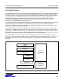
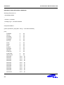
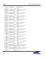
Table of Contents
Chapter 1
Product Overview
Introduction..............................................................................................................................................1-1
Features ..................................................................................................................................................1-2
Signal Descriptions ..................................................................................................................................1-6
CPU Core Overview ................................................................................................................................1-19
Instruction Set .................................................................................................................................1-20
Memory Interface ............................................................................................................................1-21
Operating States .............................................................................................................................1-21
Operating Modes.............................................................................................................................1-21
Registers .........................................................................................................................................1-22
Exceptions ......................................................................................................................................1-23
Special Registers ............................................................................................................................1-24
Chapter 2
Programmer's Model
Overview .................................................................................................................................................2-1
Switching State ...............................................................................................................................2-1
Big-Endian Format ..........................................................................................................................2-2
Little-Endian Format........................................................................................................................2-2
Instruction Length............................................................................................................................2-3
Operating Modes.............................................................................................................................2-3
Registers .........................................................................................................................................2-4
The Program Status Registers.........................................................................................................2-8
Exceptions ......................................................................................................................................2-11
S3C4520A RISC MICROCONTROLLER
iii
Table of Contents (Continued)
Chapter 3
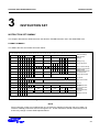
Instruction Set
Instruction Set Summay.......................................................................................................................... 3-1
Format Summary ........................................................................................................................... 3-1
Instruction Summary....................................................................................................................... 3-2
The Condition Field................................................................................................................................. 3-4
Branch and Exchange (BX)..................................................................................................................... 3-5
Instruction Cycle Times .................................................................................................................. 3-5
Assembler Syntax........................................................................................................................... 3-5
Using R15 As An Operand.............................................................................................................. 3-5
Branch and Branch With Link (B, Bl)....................................................................................................... 3-7
The Link Bit .................................................................................................................................... 3-7
Instruction Cycle Times .................................................................................................................. 3-7
Assembler Syntax........................................................................................................................... 3-8
Data Processing...................................................................................................................................... 3-9
CPSR Flags.................................................................................................................................... 3-11
Shifts.............................................................................................................................................. 3-12
Immediate Operand Rotates........................................................................................................... 3-16
Writing to R15 ................................................................................................................................ 3-16
Using R15 as an Operand............................................................................................................... 3-16
TEQ, TST, CMP and CMN Opcodes............................................................................................... 3-16
Instruction Cycle Times .................................................................................................................. 3-17
Assembler Syntax........................................................................................................................... 3-17
PSR Transfer (MRS, MSR) ..................................................................................................................... 3-19
Operand Restrictions ...................................................................................................................... 3-19
Reserved Bits ................................................................................................................................. 3-21
Instruction Cycle Times .................................................................................................................. 3-21
Assembler Syntax........................................................................................................................... 3-22
Multiply And Multiply-Accumulate (MUL, MLA)........................................................................................ 3-23
CPSR Flags.................................................................................................................................... 3-24
Instruction Cycle Times .................................................................................................................. 3-24
Assembler Syntax........................................................................................................................... 3-24
Multiply Long And Multiply-Accumulate Long (MULL,MLAL) ................................................................... 3-25
Operand Restrictions ...................................................................................................................... 3-25
CPSR Flags.................................................................................................................................... 3-26
Instruction Cycle Times .................................................................................................................. 3-26
Assembler Syntax........................................................................................................................... 3-27
Single Data Transfer (LDR, STR)............................................................................................................ 3-28
Offsets and Auto-Indexing .............................................................................................................. 3-29
Shifted Register Offset ................................................................................................................... 3-29
Bytes and Words ............................................................................................................................ 3-29
Use of R15 ..................................................................................................................................... 3-31
Restriction on The Use of Base Register......................................................................................... 3-31
Data Aborts .................................................................................................................................... 3-31
Instruction Cycle Times .................................................................................................................. 3-31
Assembler Syntax........................................................................................................................... 3-32
iv
S3C4520A RISC MICROCONTROLLER
Table of Contents (Continued)
Chapter 3
Instruction Set (Continued)
Halfword and Signed Data Transfer (LDRH/STRH/LDRSB/LDRSH).........................................................3-34
Offsets and Auto-Indexing ...............................................................................................................3-35
Halfword Load and Stores ...............................................................................................................3-36
Signed Byte and Halfword Loads.....................................................................................................3-36
Endianness and Byte/Halfword Selection.........................................................................................3-36
Use of R15 ......................................................................................................................................3-37
Data Aborts .....................................................................................................................................3-37
Instruction Cycle Times ...................................................................................................................3-37
Assembler Syntax ...........................................................................................................................3-38
Block Data Transfer (LDM, STM).............................................................................................................3-40
The Register List .............................................................................................................................3-40
Addressing Modes ...........................................................................................................................3-41
Address Alignment ..........................................................................................................................3-41
Use of The S Bit ..............................................................................................................................3-43
Use of R15 as The Base..................................................................................................................3-43
Inclusion of The Base In The Register List.......................................................................................3-44
Data Aborts .....................................................................................................................................3-44
Instruction Cycle Times ...................................................................................................................3-44
Assembler Syntax ...........................................................................................................................3-45
Single Data Swap (SWP).........................................................................................................................3-47
Bytes and Words .............................................................................................................................3-47
Use of R15 ......................................................................................................................................3-47
Data Aborts .....................................................................................................................................3-48
Instruction Cycle Times ...................................................................................................................3-48
Assembler Syntax ...........................................................................................................................3-48
Software Interrupt (SWI) ..........................................................................................................................3-49
Return From The Supervisor ...........................................................................................................3-49
Comment Field................................................................................................................................3-49
Instruction Cycle Times ...................................................................................................................3-49
Assembler Syntax ...........................................................................................................................3-50
Coprocessor Data Operations (CDP) .......................................................................................................3-51
Coprocessor Instructions .................................................................................................................3-51
The Coprocessor Fields...................................................................................................................3-51
Instruction Cycle Times ...................................................................................................................3-52
Assembler Syntax ...........................................................................................................................3-52
Coprocessor Data Transfers (LDC, STC) .................................................................................................3-53
The Coprocessor Fields...................................................................................................................3-53
Addressing Modes ...........................................................................................................................3-54
Address Alignment ..........................................................................................................................3-54
Use of R15 ......................................................................................................................................3-54
Data Aborts .....................................................................................................................................3-54
Instruction Cycle Times ...................................................................................................................3-54
Assembler Syntax ...........................................................................................................................3-55
S3C4520A RISC MICROCONTROLLER
v
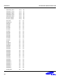
Table of Contents (Continued)
Chapter 3
Instruction Set (Continued)
Coprocessor Register Transfers (MRC, MCR)......................................................................................... 3-56
The Coprocessor Fields.................................................................................................................. 3-56
Transfers To R15............................................................................................................................ 3-57
Transfers From R15 ....................................................................................................................... 3-57
Instruction Cycle Times .................................................................................................................. 3-57
Assembler Syntax........................................................................................................................... 3-57
Undefined Instruction .............................................................................................................................. 3-58
Instruction Cycle Times .................................................................................................................. 3-58
Assembler Syntax........................................................................................................................... 3-58
Using The Conditional Instructions.................................................................................................. 3-59
Pseudo-Random Binary Sequence Generator................................................................................. 3-61
Multiplication By Constant Using The Barrel Shifter ........................................................................ 3-61
Thumb Instruction Set Format................................................................................................................. 3-64
Format Summary ........................................................................................................................... 3-64
Opcode Summary .......................................................................................................................... 3-65
Format 1: Move Shifted Register ............................................................................................................ 3-67
Operation ....................................................................................................................................... 3-67
Instruction Cycle Times .................................................................................................................. 3-67
Format 2: Add/Subtract........................................................................................................................... 3-68
Operation ....................................................................................................................................... 3-68
Instruction Cycle Times .................................................................................................................. 3-69
Format 3: Move/Compare/Add/Subtract Immediate ................................................................................ 3-70
Operations...................................................................................................................................... 3-70
Instruction Cycle Times .................................................................................................................. 3-70
Format 4: Alu Operations........................................................................................................................ 3-71
Operation ....................................................................................................................................... 3-71
Instruction Cycle Times .................................................................................................................. 3-72
Format 5: Hi-Register Operations/Branch Exchange ............................................................................... 3-73
Operation ....................................................................................................................................... 3-73
Instruction Cycle Times .................................................................................................................. 3-74
The Bx Instruction .......................................................................................................................... 3-74
Using R15 As An Operand.............................................................................................................. 3-75
Format 6: PC-Relative Load ................................................................................................................... 3-76
Operation ....................................................................................................................................... 3-76
Instruction Cycle Times .................................................................................................................. 3-76
Format 7: Load/Store With Register Offset ............................................................................................. 3-77
Operation ....................................................................................................................................... 3-77
Instruction Cycle Times .................................................................................................................. 3-78
Format 8: Load/Store Sign-Extended Byte/Halfword ............................................................................... 3-79
Operation ....................................................................................................................................... 3-79
Instruction Cycle Times .................................................................................................................. 3-80
vi
S3C4520A RISC MICROCONTROLLER
Table of Contents (Continued)
Chapter 3
Instruction Set (Continued)
Format 9: Load/Store With Immediate Offset..........................................................................................3-81
Operation ........................................................................................................................................3-81
Instruction Cycle Times ...................................................................................................................3-82
Format 10: Load/Store Halfword ..............................................................................................................3-83
Operation ........................................................................................................................................3-83
Instruction Cycle Times ...................................................................................................................3-83
Format 11: SP-Relative Load/Store .........................................................................................................3-84
Operation ........................................................................................................................................3-84
Instruction Cycle Times ...................................................................................................................3-84
Format 12: Load Addres ..........................................................................................................................3-85
Operation ........................................................................................................................................3-85
Instruction Cycle Times ...................................................................................................................3-86
Format 13: Add Offset To Stack Pointer ..................................................................................................3-87
Operation ........................................................................................................................................3-87
Instruction Cycle Times ...................................................................................................................3-87
Format 14: Push/POP Registers ..............................................................................................................3-88
Operation ........................................................................................................................................3-88
Instruction Cycle Times ...................................................................................................................3-89
Format 15: Multiple Load/Store................................................................................................................3-90
Operation ........................................................................................................................................3-90
Instruction Cycle Times ...................................................................................................................3-90
Format 16: Conditional Branch ................................................................................................................3-91
Operation ........................................................................................................................................3-91
Instruction Cycle Times ...................................................................................................................3-92
Format 17: Software Interrupt ..................................................................................................................3-93
Operation ........................................................................................................................................3-93
Instruction Cycle Times ...................................................................................................................3-93
Format 18: Unconditional Branch.............................................................................................................3-94
Operation ........................................................................................................................................3-94
Format 19: Long Branch With Link...........................................................................................................3-95
Operation ........................................................................................................................................3-95
Instruction Cycle Times ...................................................................................................................3-96
Instruction Set Examples .........................................................................................................................3-97
Multiplication By a Constant Using Shifts And Adds.........................................................................3-97
Division by a Constant.....................................................................................................................3-100
S3C4520A RISC MICROCONTROLLER
vii
Table of Contents (Continued)
Chapter 4
System Manager
Overview ................................................................................................................................................ 4-1
System Manager Registers............................................................................................................. 4-2
External Address Translation Method Depends on the Width of External Memory .......................... 4-6
Connection of External Memory With Various Data Width .............................................................. 4-7
Endian Modes................................................................................................................................. 4-8
BUS Arbitration............................................................................................................................... 4-15
Control Registers .................................................................................................................................... 4-16
System Configuration Register (SYSCFG)...................................................................................... 4-16
Product Code and Revision Number Register (PROREV)............................................................... 4-18
Peripheral & SDRAM Clock Enable Register (CER)........................................................................ 4-19
Watch Dog Timer Register (WDT).................................................................................................. 4-20
System Clock and Mux Bus Control Register .......................................................................................... 4-22
Clock Control Register (CLKCON) .................................................................................................. 4-22
System Clock ................................................................................................................................. 4-23
USB 48 MHz Clock......................................................................................................................... 4-24
External I/O Access Control Registers (EXTACON0/1) ................................................................... 4-26
ROM/SRAM/FLASH Control Registers (ROMCON) ........................................................................ 4-32
DRAM Control Registers................................................................................................................. 4-37
DRAM Interface Features ............................................................................................................... 4-45
DRAM Bank Space......................................................................................................................... 4-47
DRAM Refresh and External I/O Control Register........................................................................... 4-49
Chapter 5
Unified Instruction/Data Cache
Overview ................................................................................................................................................ 5-1
Cache Configuration....................................................................................................................... 5-1
Cache Replace Operations ............................................................................................................. 5-3
Cache Disable/Enable .................................................................................................................... 5-4
Cache Flush Operation................................................................................................................... 5-4
Non-Cacheable Area Control Bit..................................................................................................... 5-4
viii
S3C4520A RISC MICROCONTROLLER
Table of Contents (Continued)
Chapter 6
HDLC Controller
Overview .................................................................................................................................................6-1
Features ..................................................................................................................................................6-2
Function Descriptions ......................................................................................................................6-3
HDLC Frame Format.......................................................................................................................6-4
Protocol Features ....................................................................................................................................6-6
Invalid Frame ..................................................................................................................................6-6
Zero Insertion and Zero Deletion .....................................................................................................6-6
Abort ...............................................................................................................................................6-6
Idle and Time Fill.............................................................................................................................6-6
FIFO Structure ................................................................................................................................6-7
DMA Support...................................................................................................................................6-7
Baud Rate Generator ......................................................................................................................6-7
Digital Phase-Locked Loop (DPLL) ..................................................................................................6-9
Clock Usage Method .......................................................................................................................6-9
HDLC Operational Description .................................................................................................................6-11
HDLC Initialization...........................................................................................................................6-11
HDLC Data Encoding/Decoding.......................................................................................................6-12
HDLC Data Setup and Hold Timing With Clock ...............................................................................6-13
HDLC Transmitter Operation ...........................................................................................................6-14
HDLC Receiver Operation...............................................................................................................6-16
Transparent Operation.....................................................................................................................6-17
Hardware Flow Control ....................................................................................................................6-18
HDLC Special Registers ..................................................................................................................6-20
HDLC Global Mode Register ...........................................................................................................6-23
HDLC Control Register ....................................................................................................................6-26
HDLC Status Register (HSTAT).......................................................................................................6-32
Summary ........................................................................................................................................6-32
HDLC Interrupt Enable Register (HINTEN) ......................................................................................6-37
HDLC Tx FIFO (HTXFIFO)..............................................................................................................6-39
HDLC Rx FIFO (HRXFIFO) .............................................................................................................6-40
HDLC BRG Time Constant Registers (HBRGTC) ............................................................................6-41
HDLC Preamble Constant Register (HPRMB) .................................................................................6-42
HDLC Station Address Registers (HSADR0-3) and HMASK Register ..............................................6-43
Received Byte Count Register.........................................................................................................6-45
HDLC Synchronization Register ......................................................................................................6-46
Chapter 7
IOM2 Controller
Features ..................................................................................................................................................7-1
IOM2 Bus ................................................................................................................................................7-2
Channel Operation ..........................................................................................................................7-4
Pin Direction Reversal.....................................................................................................................7-9
IOM2 Special Registers...................................................................................................................7-9
S3C4520A RISC MICROCONTROLLER
ix
Table of Contents (Continued)
Chapter 8
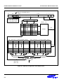
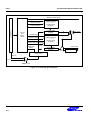
TSA (Timer Slot Assigner)
Overview ................................................................................................................................................ 8-1
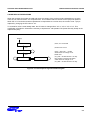
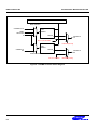
TSA Block Diagram ........................................................................................................................ 8-2
HDLC External Pin Multiplexed Signals .......................................................................................... 8-3
Operation ....................................................................................................................................... 8-3
TSA Special Registers.................................................................................................................... 8-4
Chapter 9
DMA Controller
Overview ................................................................................................................................................ 9-1
GDMA Special Registers ................................................................................................................ 9-3
GDMA Source/Destination Address Registers................................................................................. 9-8
DMA Transfer Count Registers ....................................................................................................... 9-9
DMA Mode Operation ..................................................................................................................... 9-10
GDMA Function Description.................................................................................................................... 9-11
GDMA Transfers............................................................................................................................. 9-11
Starting/Ending GDMA Transfers.................................................................................................... 9-11
Data Transfer Modes ...................................................................................................................... 9-11
DMA Transfer Timing Data ............................................................................................................. 9-13
Clock Description............................................................................................................................ 9-14
Single and One Data Burst Mode (GDMACON[11] = 0, [9] = 0) ...................................................... 9-15
Single and Four Data Burst Mode (GDMACON[11] = 0, [9] = 1)...................................................... 9-16
Block and One Data Burst Mode (GDMACON[11] = 1, [9] = 0) ....................................................... 9-17
Block and Four Data Burst (GDMACON[11] = 1, [9] = 1) ................................................................ 9-17
Continuous and One Burst Mode (GDMACON[14] = 1, [9] = 0)....................................................... 9-18
Continuous and Four Data Burst Mode (GDMACON[14] = 1, [9] = 1).............................................. 9-18
Demand and One Data Burst Mode (GDMACON[15] = 1, [9] = 0)................................................... 9-19
Demand & Four Data Burst Mode (GDMACON[15] = 1, [9] = 1)...................................................... 9-19
Chapter 10
UART
Overview ................................................................................................................................................ 10-1
UART Special Registers ......................................................................................................................... 10-3
UART Control Registers ................................................................................................................. 10-4
UART Status Registers................................................................................................................... 10-9
UART Transmit Buffer Register ...................................................................................................... 10-16
UART Receive Buffer Register ....................................................................................................... 10-17
UART Baud Rate Divisor Register .................................................................................................. 10-18
UART Baud Rate Examples ........................................................................................................... 10-19
UART Control Character 1 Register................................................................................................ 10-20
UART Control Character 2 Register................................................................................................ 10-21
UART Operation............................................................................................................................. 10-22
x
S3C4520A RISC MICROCONTROLLER
Table of Contents (Continued)
Chapter 11
USB
USB Features ..........................................................................................................................................11-1
USB BUS Topology and Physical Connection..................................................................................11-1
Frame Generation ...........................................................................................................................11-2
Packet Formats ...............................................................................................................................11-4
Bit Stuffing and NRZI Coding ..........................................................................................................11-5
BULK Transactions..........................................................................................................................11-5
Control Transactions .......................................................................................................................11-5
Isochronous Transactions ................................................................................................................11-6
Interrupt Transactions......................................................................................................................11-6
S3C4520A USB Block Overview..............................................................................................................11-7
S3C4520A USB Function Features..........................................................................................................11-10
USB Function Address Register ......................................................................................................11-12
USB Power Management Register ..................................................................................................11-13
USB Endpoint Interrupt Register......................................................................................................11-15
For ISO Endpoints:..........................................................................................................................11-15
USB Interrupt Register.............................................................................................................................11-17
USB Endpoint Interrupt Enable Register..........................................................................................11-19
USB Interrupt Enable Register.........................................................................................................11-21
USB Frame Number Register 1, 2 ...................................................................................................11-23
USB Index Register.........................................................................................................................11-25
USB Disconnect Register ................................................................................................................11-27
USB In CSR Register 1 (ENDPOINT 0) ...........................................................................................11-31
USB In CSR Register 1 (ENDPOINT1-ENDPOINT4).......................................................................11-34
USB In CSR Register 2 ...................................................................................................................11-37
USB Out CSR Register1, 2..............................................................................................................11-39
USB Out Write Count Register 1,2 ..................................................................................................11-43
USB FIFO Register .........................................................................................................................11-45
Chapter 12
32-Bit Timers
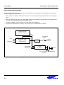
Overview .................................................................................................................................................12-1
Interval Mode Operation..................................................................................................................12-1
Toggle Mode Operation...................................................................................................................12-1
Timer Operation Guidelines.............................................................................................................12-2
Timer Mode Register.......................................................................................................................12-3
Timer Data Registers.......................................................................................................................12-4
Timer Count Registers.....................................................................................................................12-4
S3C4520A RISC MICROCONTROLLER
xi
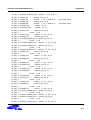
Table of Contents (Concluded)
Chapter 13
I/O Ports
Overview ................................................................................................................................................ 13-1
I/O Port Special Registers....................................................................................................................... 13-2
I/O Port Mode Register (IOPMOD0/1)............................................................................................. 13-2
I/O Port Control Register (IOPCON0/1/2) ....................................................................................... 13-4
I/O Port Data Register (IOPDATA0/1)............................................................................................. 13-9
Chapter 14
Interrupt Controller
Overview ................................................................................................................................................ 14-1
Interrupt Sources .................................................................................................................................... 14-2
Interrupt Controller Special Registers...................................................................................................... 14-3
Interrupt Mode Register .................................................................................................................. 14-3
Interrupt Pending Register .............................................................................................................. 14-4
Interrupt Mask Register................................................................................................................... 14-5
Interrupt Priority Registers .............................................................................................................. 14-6
Interrupt Offset Register ................................................................................................................. 14-7
Interrupt Pending By Priority Register ............................................................................................. 14-8
Interrupt Pending Test Register ...................................................................................................... 14-8
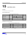
Chapter 15
Electrical Data
Overview ................................................................................................................................................ 15-1
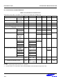
Absolute Maximum Ratings ............................................................................................................ 15-1
Recommended Operating Conditions ............................................................................................. 15-1
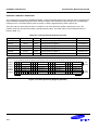
D.C. Electrical Characteristics ........................................................................................................ 15-2
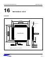
Chapter 16
Mechanical Data
Overview ................................................................................................................................................ 16-1
Appendix A
Test Access Port..................................................................................................................................... A-1
Boundary Scan Register ................................................................................................................. A-3
Instruction Register......................................................................................................................... A-3
Boundary Scan Definition Language............................................................................................... A-4
xii
S3C4520A RISC MICROCONTROLLER
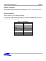
List of Figures
Figure
Number
Title
Page
Number
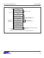
1-1
1-2
1-3
1-4
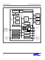
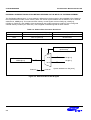
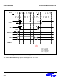
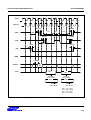
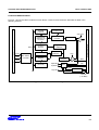
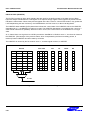
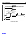
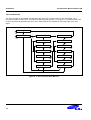
S3C4520A Block Diagram ......................................................................................1-4
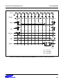
S3C4520A Pin Assignment Diagram ......................................................................1-5
Reset Timing Diagram............................................................................................1-18
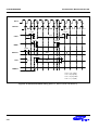
ARM7TDMI Core Block Diagram ............................................................................1-19
2-1
2-2
2-3
2-4
2-5
2-6
Big-Endian Addresses of Bytes within Words..........................................................2-2
Little-Endian Addresses of Bytes Words .................................................................2-2
Register Organization in ARM State .......................................................................2-5
Register Organization in THUMB State ..................................................................2-6
Mapping of THUMB State Registers onto ARM State Registers..............................2-7
Program Status Register Format ............................................................................2-8
3-1
3-2
3-3
3-4
3-5
3-6
3-7
3-8
3-9
3-10
3-11
3-12
3-13
3-14
3-15
3-16
3-17
3-18
3-19
3-20
3-21
3-22
3-23
3-24
3-25
3-26
3-27
3-28
3-29
3-30
3-31
3-32
3-33
3-34
3-35
ARM Instruction Set Format ...................................................................................3-1
Branch and Exchange Instructions..........................................................................3-5
Branch Instructions.................................................................................................3-7
Data Processing Instructions ..................................................................................3-9
ARM Shift Operations.............................................................................................3-12
Logical Shift Left ....................................................................................................3-12
Logical Shift Right ..................................................................................................3-13
Arithmetic Shift Right .............................................................................................3-13
Rotate Right ...........................................................................................................3-14
Rotate Right Extended ...........................................................................................3-14
PSR Transfer .........................................................................................................3-20
Multiply Instructions................................................................................................3-23
Multiply Long Instructions .......................................................................................3-25
Single Data Transfer Instructions............................................................................3-28
Little-Endian Offset Addressing ..............................................................................3-30
Halfword and Signed Data Transfer with Register Offset ........................................3-34
Halfword and Signed Data Transfer with Immediate Offset and Auto-Indexing .......3-35
Block Data Transfer Instructions.............................................................................3-40
Post-Increment Addressing.....................................................................................3-41
Pre-Increment Addressing ......................................................................................3-42
Post-Decrement Addressing ...................................................................................3-42
Pre-Decrement Addressing.....................................................................................3-43
Swap Instruction.....................................................................................................3-47
Software Interrupt Instruction..................................................................................3-49
Coprocessor Data Operation Instruction .................................................................3-51
Coprocessor Data Transfer Instructions ..................................................................3-53
Coprocessor Register Transfer Instructions ............................................................3-56
Undefined Instruction..............................................................................................3-58
THUMB Instruction Set Formats .............................................................................3-64
Format 1 ................................................................................................................3-67
Format 2 ................................................................................................................3-68
Format 3 ................................................................................................................3-70
Format 4 ................................................................................................................3-71
Format 5 ................................................................................................................3-73
Format 6 ................................................................................................................3-76
S3C4520A RISC MICROCONTROLLER
xiii
List of Figures (Continued)
Figure
Number
Title
Page
Number
3-36
3-37
3-38
3-39
3-40
3-41
3-42
3-43
3-44
3-45
3-46
3-47
3-48
Format 7................................................................................................................ 3-77
Format 8................................................................................................................ 3-79
Format 9................................................................................................................ 3-81
Format 10.............................................................................................................. 3-83
Format 11.............................................................................................................. 3-84
Format 12.............................................................................................................. 3-85
Format 13.............................................................................................................. 3-87
Format 14.............................................................................................................. 3-88
Format 15.............................................................................................................. 3-90
Format 16.............................................................................................................. 3-91
Format 17.............................................................................................................. 3-93
Format 18.............................................................................................................. 3-94
Format 19.............................................................................................................. 3-95
4-1
4-2
4-3
4-4
4-5
4-6
4-7
4-8
4-9
4-10
4-11
4-12
4-13
4-14
4-17
4-18
4-19
4-20
4-21
4-22
4-23
4-24
4-25
4-26
4-27
4-28
4-29
4-30
4-31
4-32
4-33
S3C4520A System Memory Map........................................................................... 4-3
Initial System Memory Map (After Reset) .............................................................. 4-5
External Address Bus Diagram .............................................................................. 4-6
Data Bus Connection with External Memory .......................................................... 4-8
System Configuration Register (SYSCFG)............................................................. 4-17
Product Code and Revision Number Register (PROREV)...................................... 4-18
Peripheral & SDRAM Clock Enable Register (CER)............................................... 4-19
Watch Dog Timer Register (WDT)......................................................................... 4-20
Clock Control Register (CLKCON) ......................................................................... 4-22
System Clock Circuit ............................................................................................. 4-23
USB 48 MHz Clock Circuit..................................................................................... 4-24
Divided System Clocks Timing Diagram................................................................ 4-25
External I/O Access Control Registers (EXTACON0, EXTACON1) ........................ 4-27
External I/O Read Timing (tCOH = 1, tACC = 4, tCOS = 0, tACS = 1) .......................... 4-28
External I/O Write Timing with nEWAIT (tCOH = 1, tACC = 7, tCOS = 0, tACS = 1)..... 4-31
ROM/SRAM/FLASH Control Registers (ROMCON0 – ROMCON1) ....................... 4-33
ROM/SRAM/Flash Read Access Timing ................................................................ 4-34
ROM/Flash Page Read Access Timing .................................................................. 4-35
ROM/SRAM/Flash Write Access Timing................................................................ 4-36
DRAM Control Registers (DRAMCON0–DRAMCON1)........................................... 4-38
EDO/FP DRAM Bank Read Timing (Page Mode) .................................................. 4-39
EDO/FP DRAM Bank Write Timing (Page Mode) .................................................. 4-40
EDO/FP DRAM Bank Read/Write Timing (Page Mode) ......................................... 4-41
SDRAM Power-up Sequence................................................................................. 4-42
Non-burst, Read-Write-Read Cycles @CAS Latency = 2, Burst Length = 1 ........... 4-43
SDRAM Burst-Read............................................................................................... 4-44
SDRAM Application Example ................................................................................ 4-48
DRAM Refresh and External I/O Control Register (REFEXTCON)......................... 4-50
External I/O Bank Address Map............................................................................. 4-51
EDO/FP DRAM Refresh Timing............................................................................. 4-52
Auto Refresh Cycle of SDRAM .............................................................................. 4-53
xiv
S3C4520A RISC MICROCONTROLLER
List of Figures (Continued)
Figure
Number
Title
Page
Number
5-1
5-2
Memory Configuration for 4-Kbyte Cache...............................................................5-2
Cache Replace Algorithm State Diagram ...............................................................5-3
6-1
6-2
6-3
6-4
6-5
6-6
6-7
6-8
6-9
6-10
6-11
6-12
6-13
6-14
6-15
6-16
6-17
6-18
6-19
6-20
6-21
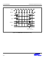
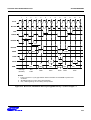
HDLC Module Block Diagram.................................................................................6-3
Baud Rate Generator Block Diagram......................................................................6-7
DPLL Block Diagram ..............................................................................................6-9
Clock Usage Method Diagram ................................................................................6-9
Data Encoding Methods and Timing Diagrams .......................................................6-12
Data Setup and Hold Timing Diagrams...................................................................6-13
nCTS already Asserted...........................................................................................6-18
CTS Lost during Transmission................................................................................6-18
CTS Delayed on .....................................................................................................6-19
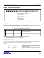
HMODE Register....................................................................................................6-25
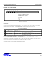
HDLC Control Register (HCON) .............................................................................6-30
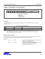
HDLC Status Register ............................................................................................6-35
HDLC Interrupt Enable Register .............................................................................6-38
HDLC Tx FIFO Function Diagram ..........................................................................6-39
HDLC Rx FIFO Function Diagram ..........................................................................6-40
HDLC BRG Time Constant Register.......................................................................6-41
HDLC Preamble Constant Register ........................................................................6-42
Address Recognition...............................................................................................6-43
HDLC Station Address and HMASK Register..........................................................6-44
Received Byte Count Register................................................................................6-45
HDLC Synchronization Register .............................................................................6-46
7-1
7-2
7-3
7-4
7-5
7-6
7-7
7-8
7-9
7-10
7-11
7-12
7-13
7-14
7-15
7-16
7-17
7-18
IOM2 Channel Structure in Terminal ......................................................................7-2
Monitor Channel Handshake Protocol.....................................................................7-4
Abortion of Monitor Channel Transmission .............................................................7-5
Structure of Last Byte of Channel 2 on DU .............................................................7-7
Structure of Last Byte of Channel 2 on DD .............................................................7-8
IOM2 Control Register............................................................................................7-11
IOM2 Status Register .............................................................................................7-13
IOM2 Interrupt Enable Register ..............................................................................7-15
IOM2 TIC Bus Address Register.............................................................................7-16
IOM2 IC Channel Transmit Data Register...............................................................7-17
IOM2 IC Channel Receive Data Register................................................................7-17
IOM2 C/I0 Channel Transmit Data Register............................................................7-18
IOM2 C/I0 Channel Receive Data Register.............................................................7-18
IOM2 C/I1 Channel Transmit Data Register............................................................7-19
IOM2 C/I1 Channel Receive Data Register.............................................................7-19
IOM2 Monitor Channel Transmit Data Register ......................................................7-20
IOM2 Monitor Channel Receive Data Register .......................................................7-20
IOM2 Strobe Register.............................................................................................7-21
S3C4520A RISC MICROCONTROLLER
xv
List of Figures (Continued)
Figure
Number
Title
Page
Number
8-1
8-2
8-3
8-4
TSA Block Diagram ............................................................................................... 8-2
TSA A Configuration Register................................................................................ 8-4
TSA B Configuration Register................................................................................ 8-5
TSA C Configuration Register................................................................................ 8-6
9-1
9-2
9-3
9-4
9-5
9-6
9-7
9-8
9-9
9-10
9-11
9-12
9-13
9-14
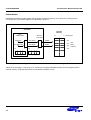
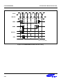
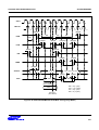
GDMA Controller Block Diagram ........................................................................... 9-2
GDMA Control Register ......................................................................................... 9-7
GDMA Source/Destination Address Register ......................................................... 9-8
DMA Transfer Count Register................................................................................ 9-9
External DMA Requests (Single Mode).................................................................. 9-11
External DMA Requests (Block Mode) ................................................................... 9-12
External DMA Requests (Demand Mode) .............................................................. 9-12
External DMA Requests Detailed Timing ............................................................... 9-13
MCLKO and SCLK(In_MCLK)................................................................................ 9-14
Single and One Data Burst Mode Timing............................................................... 9-15
Single and Four Data Burst Mode Timing .............................................................. 9-16
Block and One Data Burst Mode Timing ................................................................ 9-17
Continuous and One Burst Mode Timing ............................................................... 9-18
Demand and One Data Burst Mode Timing ........................................................... 9-19
10-1
10-2
10-3
10-4
10-5
10-6
10-7
10-8
10-9
10-10
10-11
10-12
10-13
10-14
10-15
10-16
10-17
10-18
10-19
10-20
Serial I/O Block Diagram ....................................................................................... 10-2
UART Control Register .......................................................................................... 10-7
UART Status Register ........................................................................................... 10-12
UART Interrupt Enable Register ............................................................................ 10-15
UART Transmit Buffer Register ............................................................................. 10-16
UART Receive Buffer Register .............................................................................. 10-17
UART Baud Rate Divisor Register ......................................................................... 10-18
UART Baud Rate Generator (BRG) ....................................................................... 10-19
UART Control Character 1 Register....................................................................... 10-20
UART Control Character 2 Register....................................................................... 10-21
When Signal is Asserted During Transmit Operation ............................................. 10-23
When CTS Signal is Deasserted During Transmit Operation ................................. 10-23
Normal Received Rx Data ..................................................................................... 10-24
CD Lost During Rx Data Receive........................................................................... 10-24
Interrupt-Based Serial I/O Timing Diagram (Tx and Rx Only) ................................ 10-25
DMA-Based Serial I/O Timing Diagram (Tx Only).................................................. 10-26
DMA-Based Serial I/O Timing Diagram (Rx Only) ................................................. 10-26
Serial I/O Frame Timing Diagram (Normal UART)................................................. 10-27
Infra-Red Transmit Mode Frame Timing Diagram.................................................. 10-27
Infra-Red Receive Mode Frame Timing Diagram................................................... 10-28
xvi
S3C4520A RISC MICROCONTROLLER
List of Figures (Concluded)
Figure
Number
Title
Page
Number
11-1
11-2
11-3
11-4
11-5
11-6
11-7
11-8
11-9
11-10
11-11
11-12
11-13
11-14
11-15
11-16
11-17
11-18
11-19
11-20
11-21
11-22
11-23
SOF Packets ..........................................................................................................11-2
Frame Model..........................................................................................................11-3
USB Frame Format ................................................................................................11-4
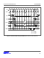
USB Core Block Diagram .......................................................................................11-7
SIE Block Diagram .................................................................................................11-9
USBFA Register .....................................................................................................11-12
USBPM Register ....................................................................................................11-14
USBEPINT Register ...............................................................................................11-16
USBINT Register....................................................................................................11-18
USBEPINTE Register.............................................................................................11-20
USBINTE Register .................................................................................................11-22
USBFNL/USBFNH Registers..................................................................................11-24
USBIDX Register....................................................................................................11-26
USBDISCONNECT Register ..................................................................................11-28
USBMAXP Register................................................................................................11-30
USBICSR1 (EP0) Register .....................................................................................11-33
USBICSR1 Register ...............................................................................................11-36
USBICSR2 Register ...............................................................................................11-38
USBOCSR1 Register .............................................................................................11-41
USBOCSR2 Register .............................................................................................11-42
USBOWCL/USBOWCH Registers..........................................................................11-44
USBEP0/USBEP1/USBEP2 FIFO Registers...........................................................11-46
USBEP3/USBEP4 FIFO Registers .........................................................................11-46
12-1
12-2
12-3
12-4
12-5
Timer Output Signal Timing....................................................................................12-1
32-Bit Timer Block Diagram ...................................................................................12-2
Timer Mode Register (TMOD) ................................................................................12-3
Timer Data Registers (TDATA0, TDATA1) .............................................................12-4
Timer Counter Registers (TCNT0, TCNT1).............................................................12-4
13-1
13-2
13-3
13-4
13-6
13-7
13-9
13-10
I/O Port Function Diagram......................................................................................13-1
I/O Port Mode Register (IOPMOD0) .......................................................................13-2
I/O Port Mode Register (IOPMOD1) .......................................................................13-3
I/O Port Control Register 0 (IOPCON0) ..................................................................13-5
I/O Port Control Register 2 (IOPCON2) ..................................................................13-8
I/O Port Data Register0 (IOPDATA0)......................................................................13-9
External Interrupt Request Timing (Active High).....................................................13-10
External Interrupt Request Timing (Active Low)......................................................13-10
14-1
14-2
14-3
14-4
Interrupt Mode Register (INTMOD).........................................................................14-3
Interrupt Pending Register (INTPND)......................................................................14-4
Interrupt Mask Register (INTMSK)..........................................................................14-5
Interrupt Priority Register (INTPRIn).......................................................................14-6
A-1
TAP Controller State Machine ................................................................................A-2
S3C4520A RISC MICROCONTROLLER
xvii
List of Tables
Table
Number
Title
Page
Number
1-1
1-2
1-3
1-4
1-5
S3C4520A Signal Descriptions ...............................................................................1-6
S3C4520A Pin List and PAD Type..........................................................................1-13
S3C4520A PAD Type.............................................................................................1-17
S3C4520A CPU Exceptions ...................................................................................1-23
S3C4520A Special Registers..................................................................................1-24
2-1
2-2
2-3
PSR Mode Bit Values .............................................................................................2-10
Exception Entry/Exit ...............................................................................................2-12
Exception Vectors ..................................................................................................2-14
3-1
3-2
3-3
3-4
3-5
3-6
3-7
3-8
3-9
3-10
3-11
3-12
3-13
3-14
3-15
3-16
3-17
3-18
3-19
3-20
3-21
3-22
3-23
3-24
3-25
3-26
The ARM Instruction Set ........................................................................................3-2
Condition Code Summary ......................................................................................3-4
ARM Data Processing Instructions..........................................................................3-11
Incremental Cycle Times........................................................................................3-17
Assembler Syntax Descriptions ..............................................................................3-27
Addressing Mode Names........................................................................................3-45
THUMB Instruction Set Opcodes ............................................................................3-65
Summary of Format 1 Instructions..........................................................................3-67
Summary of Format 2 Instructions..........................................................................3-68
Summary of Format 3 Instructions..........................................................................3-70
Summary of Format 4 Instructions..........................................................................3-71
Summary of Format 5 Instructions..........................................................................3-74
Summary of PC-Relative Load Instruction..............................................................3-76
Summary of Format 7 Instructions..........................................................................3-77
Summary of format 8 instructions...........................................................................3-79
Summary of Format 9 Instructions..........................................................................3-81
Halfword Data Transfer Instructions........................................................................3-83
SP-Relative Load/Store Instructions .......................................................................3-84
Load Address .........................................................................................................3-85
The ADD SP Instruction .........................................................................................3-87
PUSH and POP Instructions ...................................................................................3-88
The Multiple Load/Store Instructions.......................................................................3-90
The Conditional Branch Instructions .......................................................................3-91
The SWI Instruction................................................................................................3-93
Summary of Branch Instruction ..............................................................................3-94
The BL Instruction ..................................................................................................3-96
List of Tables (Continued)
Table
Number
Title
Page
Number
4-1
4-2
4-3
4-4
4-5
4-6
4-7
4-8
4-9
4-10
4-11
4-12
4-13
4-14
4-15
4-16
4-17
4-18
4-19
4-20
4-21
4-22
4-23
4-24
4-25
4-26
System Manager Registers.................................................................................... 4-5
Address Bus Generation Guidelines ...................................................................... 4-6
Word Access Store Operation with Big-Endian ...................................................... 4-9
Word Access Load Operation with Big-Endian....................................................... 4-9
Half-Word Access Store Operation with Big-Endian............................................... 4-10
Half-Word Access Load Operation with Big-Endian ............................................... 4-10
Byte Access Store Operation with Big-Endian........................................................ 4-11
Byte Access Load Operation with Big-Endian ........................................................ 4-11
Word Access Store Operation with Little-Endian.................................................... 4-12
Word Access Load Operation with Little-Endian .................................................... 4-12
Half-Word Access Store Operation with Little-Endian ............................................ 4-13
Half-Word Access Load Operation with Little-Endian ............................................. 4-13
Byte Access Store Operation with Little-Endian ..................................................... 4-14
Byte Access Load Operation with Little-Endian ...................................................... 4-14
Bus Priorities for Arbitration ................................................................................... 4-15
SYSCFG Register ................................................................................................. 4-16
PROREV Register ................................................................................................. 4-18
CER Register ........................................................................................................ 4-19
WDT Register........................................................................................................ 4-20
Watch Dog Timer Timeout Value (WDTVAL, X : Don't Care)................................ 4-21
CLKCON Register ................................................................................................. 4-22
CLKCON Register Description............................................................................... 4-22
External I/O Access Control Register Description .................................................. 4-26
ROM/SRAM/Flash Control Register Description .................................................... 4-32
DRAM and External I/O Control Register Description ............................................ 4-37
CAN and Address MUX Output.............................................................................. 4-47
6-1
6-2
6-3
6-4
6-5
6-6
6-7
6-8
6-9
6-10
6-11
6-12
6-13
6-14
6-15
6-16
6-17
6-18
6-19
6-20
HDLC Data Frame Format..................................................................................... 6-4
Baud Rate Example of HDLC ................................................................................ 6-8
HDLC SETUP and HOLD Time Table.................................................................... 6-13
HDLC Channel A Special Registers ...................................................................... 6-20
HDLC Channel B Special Registers ...................................................................... 6-21
HDLC Channel C Special Registers...................................................................... 6-22
HMODEA , HMODEB and HMODEC Register....................................................... 6-23
HMODE Register Description ................................................................................ 6-23
HCONA , HCONB and HCONC Register ............................................................... 6-26
HCON Register Description ................................................................................... 6-26
HSTATA ,HSTATB and HSTATC Register ............................................................ 6-32
HSTAT Register Description.................................................................................. 6-33
HINTENA, HINTENB and HINTENC Register........................................................ 6-37
HINTEN Register Description ................................................................................ 6-37
HBRGTCA ,HBRGTCB HRBGTCC Register ......................................................... 6-41
HPRMBA ,HPRMBB and HPRMBC Register ......................................................... 6-42
Preamble Reference Pattern ................................................................................. 6-42
HSADR and HMASK Register ............................................................................... 6-43
Received Byte Count Register............................................................................... 6-45
Synchronization Register ....................................................................................... 6-46
xx
S3C4520A RISC MICROCONTROLLER
List of Tables (Continued)
Table
Number
Title
Page
Number
7-1
7-2
7-3
7-4
7-5
7-6
7-7
7-8
7-9
7-10
7-11
7-12
7-13
7-14
IOM2 Special Registers..........................................................................................7-9
IOM2CON Register (Control Register)....................................................................7-10
IOM2STAT Register (Status Register) ....................................................................7-12
IOM2INTEN Register (Interrupt Enable Register) ...................................................7-14
IOM2TBA Register (TIC Bus Address Register)......................................................7-16
IOM2ICTD (IOM2 IC Channel Transmit Data Register)...........................................7-17
IOM2ICRD (IOM2 IC Channel Receive Data Register) ...........................................7-17
IOM2CITD0 (IOM2 C/I0 Channel Transmit Data Register)......................................7-18
IOM2CIRD0 (IOM2 C/I0 Channel Receive Data Register) ......................................7-18
IOM2CITD1 (IOM2 C/I1 Channel Transmit Data Register)......................................7-19
IOM2CIRD1 (IOM2 C/I1 Channel Receive Data Register) ......................................7-19
IOM2MTD (IOM2 Monitor Channel Transmit Data Register) ...................................7-20
IOM2MRD (IOM2 Monitor Channel Receive Data Register)....................................7-20
IOM2STRB (Strobe Register) .................................................................................7-21
8-1
8-2
HDLC External Pin Multiplexed Signals..................................................................8-3
TSA Special Registers............................................................................................8-4
9-1
9-2
9-3
9-3
9-3
9-4
9-5
GDMA Special Registers Overview ........................................................................9-3
GDMACON0 and GDMACON1 Registers...............................................................9-4
GDMA Control Register Description .......................................................................9-4
GDMA Control Register Description (Continued) ....................................................9-5
GDMA Control Register Description (Continued) ....................................................9-6
GDMASRC0/1 and GDMADST0/1 Registers ..........................................................9-8
GDMACNT0/1/2/3/4/5 Registers.............................................................................9-9
10-1
10-2
10-3
10-4
10-5
10-6
10-7
10-8
10-9
10-10
10-11
10-12
10-13
10-14
10-15
UART Special Registers Overview .........................................................................10-3
UART Control Registers ........................................................................................10-4
UART Control Register Description ........................................................................10-4
UART Status Registers...........................................................................................10-9
UART Status Register Description..........................................................................10-9
UCON Interrupt Enable Registers...........................................................................10-14
UART Interrupt Enable Register Description...........................................................10-14
UXTBUF Registers .................................................................................................10-16
UART Transmit Register Description ......................................................................10-16
UXRBUF Registers.................................................................................................10-17
UART Receive Register Description .......................................................................10-17
UBRDIV0 and UBRDIV0 Registers .........................................................................10-18
Typical Baud Rates Examples of UART .................................................................10-19
CONCHAR1 Registers ...........................................................................................10-20
CONCHAR2 Registers ...........................................................................................10-21
S3C4520A RISC MICROCONTROLLER
xxi
List of Tables (Continued)
Table
Number
Title
Page
Number
11-1
11-2
11-3
11-4
11-5
11-6
11-7
11-8
11-9
11-10
11-11
11-12
11-13
11-14
11-15
11-16
11-17
11-18
11-19
11-20
11-21
11-22
11-23
11-24
11-25
11-26
11-27
11-28
11-29
11-30
11-31
11-32
USB Registers ....................................................................................................... 11-11
USB Function Address register .............................................................................. 11-12
USBFA Description................................................................................................ 11-12
USB Power Management register.......................................................................... 11-13
USBPM Description............................................................................................... 11-13
USB EndPoint INTerrupt register ........................................................................... 11-15
USBEPINT Description.......................................................................................... 11-15
USB INTerrupt register .......................................................................................... 11-17
USBINT Description .............................................................................................. 11-17
USB EndPoint INTerrupt Enable register ............................................................... 11-19
USBEPINTE Description ....................................................................................... 11-19
USB INTerrupt Enable register .............................................................................. 11-21
USBINTE Description ............................................................................................ 11-21
USB Frame Number register 1, 2........................................................................... 11-23
USBFN1, 2 Descriptions ........................................................................................ 11-23
USB INDEX register .............................................................................................. 11-25
USBIDX Description .............................................................................................. 11-25
USB DISCONNECT register.................................................................................. 11-27
USB DISCONNECT Description ............................................................................ 11-27
USB MAXP register ............................................................................................... 11-29
USBMAXP Description .......................................................................................... 11-29
USB In CSR register 1........................................................................................... 11-31
USBICSR1 (for EP0) Description........................................................................... 11-32
USB In CSR register 1........................................................................................... 11-34
USBICSR1 Description.......................................................................................... 11-35
USB In CSR register 2........................................................................................... 11-37
USBICSR2 Description.......................................................................................... 11-37
USB Out CSR register 1, 2 .................................................................................... 11-39
USBOCSR1 Description ........................................................................................ 11-39
USBOCSR2 Description ........................................................................................ 11-40
USB Out Write Count register 1, 2......................................................................... 11-43
USBEP0,1, 2, 3, 4, 5 Descriptions ......................................................................... 11-45
12-1
12-2
12-3
TMOD Register ..................................................................................................... 12-3
TDATA0 and TDATA1 Registers............................................................................ 12-4
TCNT0 and TCNT1 Registers................................................................................ 12-4
xxii
S3C4520A RISC MICROCONTROLLER
List of Tables (Concluded)
Table
Number
Title
Page
Number
13-1
13-2
13-3
13-4
13-5
13-6
13-7
IOPMOD0 Register ................................................................................................13-2
IOPMOD1 Register ................................................................................................13-3
IOPCON0 Register.................................................................................................13-4
IOPCON1 Register.................................................................................................13-6
IOPCON2 Register.................................................................................................13-7
IOPDATA0 Register ...............................................................................................13-9
IOPDATA1 Register ...............................................................................................13-9
14-1
14-2
14-3
14-4
14-5
14-6
14-7
14-8
S3C4520A Interrupt Sources ..................................................................................14-2
INTMOD Register...................................................................................................14-3
INTPND Register....................................................................................................14-4
INTMSK Register ...................................................................................................14-5
Interrupt Priority Register Overview........................................................................14-6
INTOFFSET Register .............................................................................................14-7
INTPNDPRI Register..............................................................................................14-8
INTPNDTST Register .............................................................................................14-8
15-1
15-2
15-3
15-4
Absolute Maximum Ratings....................................................................................15-1
Recommended Operating Conditions .....................................................................15-1
D.C Electrical Characteristics .................................................................................15-2
A.C Electrical Characteristics .................................................................................15-3
A-1
Public Instructions ..................................................................................................A-3
S3C4520A RISC MICROCONTROLLER
xxiii
S3C4520A RISC MICROCONTROLLER
1
PRODUCT OVERVIEW
PRODUCT OVERVIEW
INTRODUCTION
Samsung's S3C4520A 16/32-bit RISC microcontroller is a cost-effective, high-performance microcontroller
solution for ISDN TA (Integrated Service Digital Network Terminal Adaptor). Also provides the full-rate USB
(Universal Serial Bus) function.
The S3C4520A is built around an outstanding CPU core: the 16/32-bit ARM7TDMI RISC processor designed by
Advanced RISC Machines, Ltd. The ARM7TDMI core is a low-power, general purpose, microprocessor macrocell that was developed for use in application-specific and custom-specific integrated circuits. Its simple, elegant,
and fully static design is particularly suitable for cost-sensitive and power-sensitive applications.
Most of the on-chip function blocks have been designed using the Verilog HDL synthesizer and the S3C4520A
has been fully verified in Samsung's state-of-the-art ASIC test environment. Important peripheral functions
include six channel general-purpose DMAs, IOM-2 Interface by three channel HDLCs with transparent mode, one
UART with autobaud detection, a USB peripheral controller, two 32-bit timers, one 16-bit watchdog timer, and 38
programmable I/O ports. On-chip logic includes an interrupt controller, DRAM controller, and a controller for
ROM/SRAM and flash memory. The System Manager includes an internal 32-bit system bus arbiter and an
external memory controller.
The following integrated on-chip functions are described in detail in this user's manual:
•
Architecture
•
System Manager
•
Unified Instruction/Data Cache
•
HDLC with Transparent Mode
•
IOM2 Interface
•
TSA(Time Slot Assigner)
•
General Purpose DMA
•
UART
•
USB Interface
•
32-bit Timer
•
Programmable I/O Ports
•
Interrupt controller
•
Electrical Data
1-1
PRODUCT OVERVIEW
S3C4520A RISC MICROCONTROLLER
FEATURES
Architecture
IOM-2 Interface
•
16/32-bit RISC ARM7TDMI embedded
•
IOM2 TE mode
•
Little/Big-Endian mode supported Basically,
the internal architecture is big-endian.
So, the little-endian mode only support for
external memory.
•
TIC bus support
•
Monitor channel collision control
•
Cost-effective JTAG-based debug solution
•
Boundary scan
Three HDLCs
•
HDLC protocol features:
– Flag detection and synchronization
System Manager
– Zero insertion and deletion
•
8/16-bit external bus support for ROM/SRAM,
flash memory, DRAM, and external I/O
– Idle detection and transmission
•
Support for 2-bank SRAM/ROM/Flash
– Abort detection and transmission
•
Support for 2-bank EDO/Normal or SDRAM
•
Address search mode (expandable to 4 bytes)
•
Support for 4-bank external I/Os
•
Selectable CRC or No CRC mode
•
Programmable access cycle (0-7 wait cycles)
•
Automatic CRC generator preset
•
4-word depth write buffer
•
Digital PLL block for clock recovery
•
Cost-effective memory-to-peripheral DMA
interface
•
Programmable baud rate generator
•
NRZ/NRZI/FM/Manchester data formats for
Tx/Rx
•
Loop-back and auto-echo modes
•
8-word (8 x 32-bit) Tx/Rx FIFOs with
programmable trigger level, 1- or 4-word
•
GDMA-based or Interrupt-based operation
General-Purpose DMAs
•
Data alignment logic
•
6-channel general-purpose DMAs
•
Endian translation
•
Can be used for data transfer from memory or
I/O to memory or I/O and from UART or HDLCs
to memory or I/O, or vice versa.
•
Programmable interrupts
•
Modem interface
•
Hardware flow control
•
HDLC frame length based on octets
•
Transparant mode
Unified Instruction/Data Cache
•
Two-way, set-associative, unified 4-Kbyte cache
•
Support for LRU (least recently used) protocol
•
1-2
The DMA request sources are the external DMA
request 0-5, UART, and HDLC A, B, C.
– FCS encoding and detection (16-bit)
S3C4520A RISC MICROCONTROLLER
PRODUCT OVERVIEW
One UART
Interrupt Controller
•
•
•
•
•
•
•
•
•
•
•
•
•
•
32-byte FIFO for each Rx and Tx supported
programmable trigger level with timer
Up to 460Kbps baudrate
Automatic baudrate detection
Hardware flow control
Eight control character comparison for software
control
GDMA-based or Interrupt-based operation
Programmable transmit and receive data length
(5-8 bits)
Programmable baud rates
Programmable 1 or 2 stop bits
Odd/even/force/no parity mode
Break generation and detection
Parity, overrun, and frame error detection
— x 16 clock mode
Infra-red (IR) Tx/Rx support (IrDA)
•
•
23 interrupt request sources, i.e.,
6 for three HDLCs, 2 for two Timers,
6 for six GDMAs, 2 for one UART,
4 external interrupt request, 1 for USB,
1 for WatchDog Timer, and 1 for IOM-2.
Normal or fast interrupt mode (IRQ, FIQ)
Prioritized interrupt handling
16-bit Watchdog Timer
•
Useful for periodic reset or interrupts
Programmable I/O Ports
•
•
•
38 programmable I/O ports
Pins individually configurable to input, output, or
I/O mode for dedicated signals
4 external interrupt request input with 3-tap
filtering
PLL0 for system clock
USB with Transceiver
•
•
•
•
•
•
•
•
USB specification 1.1 compliant
Full speed 12Mbps operation with internal
transceiver only
Use interrupts to handle FIFO data for any
endpoint.
1 control endpoint with 64-byte FIFO (EP0),
2 interrupt enpoint with 16-byte FIFO (EP1/2),
and 2 data endpoints with
64-byte FIFOs (EP3 and EP4)
Data endpoints are programmable as to
direction (IN or OUT), transfer type
(bulk, or interrupt),
and maximum packet size
The maximum packet size (MAXP) of EP3 and
EP4 can be programmed to 8, 16, 32 or 64bytes
Fully integrated transceiver
Supports USB peripheral function,
not host or hub functions
Two 32-bit Timers
•
Interval mode or toggle mode operation
•
•
•
The external clock can be multiplied by on-chip
PLL to provide high frequency system clock
The input frequency range is 10-40MHz
The output frequency is 5 times of input clock.
To get 50MHz, input clock frequency should be
10MHz.
PLL1 for USB
•
•
•
The external clock can be multiplied by on-chip
PLL to provide high frequency USB clock
The input frequency range is 10-40MHz
The output frequency is 4.8 times of input clock.
To get 48 MHz, input clock frequency should be
10 MHz.
Package Type
•
144 LQFP
Operating Voltage Range
•
•
3.3V ± 5%
5-V-tolerant I/O, 3.3-V output levels
Operating Frequency
•
Up to 50 MHz
1-3
PRODUCT OVERVIEW
S3C4520A RISC MICROCONTROLLER
ARM7TDMI
32-bit RISC CPU
ICE
Breaker
TAP Controller for JTAG
2-Bank
ROM
SRAM
FLASH
CPU Interface
32-bit
System Bus
32-bit
CPU
Local
Bus
4-Kbyte
Unified
Cache
4-Word
Write
Buffer
Memory
Controller
with
Refresh
Control
16-bit Bus
2-Bank
DRAM
4-Bank
External
I/O
Device
General-Purpose
DMA 0,1,2,3,4,5
Bus Rounter
4 Ext INT Req.
6 Ext GDMA Req.
6 Ext GDMA Ack.
Timer 0 Output
Timer 1 Output
General I/O ports
Interruput Controller
HDLC A
TSA
HDLC B
IOM-2
SEL
S/T
Transceiver
HDLC C
High-Speed
UART
32-bit Timer 0,1
Watchdog Timer
XCLK
MCLKO
CLKSEL
PLL 0
Full-Speed
USB
PLL 1
FILTER
USB_XCKI
USB_XCKO
USB_CLKSEL
USB_FILTER
Figure 1-1. S3C4520A Block Diagram
1-4
PC
S3C4520A RISC MICROCONTROLLER
PRODUCT OVERVIEW
VDD
XDATA8
XDATA9
XDATA10
XDATA11
XDATA12
XDATA13
VSS
XDATA14
XDATA15
UCLK/PP16
UTXD/PP17
URXD/PP18
nUDSR/PP19
VDD
nUDTR/PP20
nURTS/PP21
nUCTS/PP22
nUDCD/PP23
PP24/xINTREQ0
PP25/xINTREQ1
VSS
PP26/xINTREQ2
PP27/xINTREQ3
PP28/TOUT0
PP29/TOUT1
PP30/xDREQ0
PP31/xDACK0
VDD
PP32/xDREQ1
PP33/xDACK1
PP34/xDREQ2
PP35/xDACK2
PP36/xDREQ3/nCTSA
PP37/xDACK3/nDCDA
VSS
109
110
111
112
113
114
115
116
117
118
119
120
121
122
123
124
125
126
127
128
129
130
131
132
133
134
135
136
137
138
139
140
141
142
143
144
VDD
IOM2_DU/TXDA
IOM2_DD/RXDA
IOM2_BCL/nDTRA
IOM2_STRB/nRTSA
IOM2_FSC/TXCA
IOM2_DCL/RXCA
PP0/xDREQ4/nCTSB
PP1/xDACK4/nDCDB
VSS
PP2/TXDB
PP3/RXDB
PP4/nDTRB
PP5/nRTSB
PP6/TXCB
PP7/RXCB
PP8/xDREQ5/nCTSC
PP9/xDACK5/nDCDC
VDD
PP10/TXDC
PP11/RXDC
PP12/nDTRC
PP13/nRTSC
PP14/TXCC
PP15/RXCC
USB_SOF/_XCLKO
USB_CLKSEL
USB_XCLK
VSS_USB
USB_D+
USB_DVDD_USB
VDD_A
USB_FILTER
FILTER
VSS_A
1
2
3
4
5
6
7
8
9
10
11
12
13
14
15
16
17
18
19
20
21
22
23
24
25
26
27
28
29
30
31
32
33
34
35
36
S3C4520A
144-LQFP
108
107
106
105
104
103
102
101
100
99
98
97
96
95
94
93
92
91
90
89
88
87
86
85
84
83
82
81
80
79
78
77
76
75
74
73
VSS
XDATA7
XDATA6
XDATA5
XDATA4
XDATA3
XDATA2
VDD
XDATA1
XDATA0
ADDR21
ADDR20
ADDR19
ADDR18
VSS
ADDR17
ADDR16
ADDR15
ADDR14
ADDR13
ADDR12
VDD
ADDR11
ADDR10/AP
ADDR9
ADDR8
ADDR7
ADDR6
VSS
ADDR5
ADDR4
ADDR3
ADDR2
ADDR1
ADDR0
VDD
72
71
70
69
68
67
66
65
64
63
62
61
60
59
58
57
56
55
54
53
52
51
50
49
48
47
46
45
44
43
42
41
40
39
38
37
VSS
nWBE1/DQM1
nWBE0/DQM0
nOE
B0SIZE
nRCS1
nRCS0
VDD
nEWAIT
nECS3
nECS2
nECS1
nECS0
VSS
nDWE
CKE
nCAS1/nSDCAS
nCAS0/nSDRAS
nRAS1/nSDCS1
nRAS0/nSDCS0
VDD
LITTLE
TMODE
CLKOEN
CLKSEL
MCLKO/SDCLK
VSS
XCLK
VSS
nRESET
TDI
TMS
nTRST
TCK
TDO
VDD
Figure 1-2. S3C4520A Pin Assignment Diagram
1-5
PRODUCT OVERVIEW
S3C4520A RISC MICROCONTROLLER
SIGNAL DESCRIPTIONS
Table 1-1. S3C4520A Signal Descriptions
Signal
Pin No.
I/O Type
Description
nRESET
43
I
Not Reset. nRESET is the global reset input for the S3C4520A. For
a system reset, and to allow for internal digital filtering, nRESET
must be held to Low level for at least 64 master clock cycles. Refer
to "Figure 3. S3C4520A reset timing diagram" for more details
about reset timing.
XCLK
45
I
S3C4520A System Clock source. If CLKSEL is Low, PLL output
clock is used as the S3C4520A internal system clock. If CLKSEL is
High, XCLK is used as the S3C4520A internal system clock.
(1)
47
O
System Clock Out. The reverse phase of the internal system clock,
MCLK is monitored from this pin.
SDCLK is system clock for SDRAM
CLKSEL
48
I
Clock Select. When CLKSEL is '0'(low level),PLL output clock can
be used as the master clock. When CLKSEL is '1'(high level), The
XCLK is used as the master clock.
CLKOEN
49
I
Clock Out Enable/Disable. (See the pin description for MCLKO.)
(2)
50
I
Test Mode. The TMODE bit settings are interpreted as follows:
'0' = normal operating mode, '1' = chip test mode.
This TMODE pin also can be used to change MF of PLL..
To get 66MHz MCLK(internal system clock) from 10MHz external
input clock, '1'(high level) should be assigned to TMODE and
'0'(low level) to CLKSEL then MF will be changed to 6.6.
LITTLE
51
I
Little endian mode select pin. If LITTLE is High, S3C4520A operate
in little endian mode. If Low, then in Big endian mode. Default value
is low because this pin is pull-downed internally.
FILTER
35
AO
System Signals
MCLKO/SDCLK
TMODE
1-6
If the PLL is used, 820pF capacitor should be connected between
the pin and analog ground (VSS_A).
S3C4520A RISC MICROCONTROLLER
PRODUCT OVERVIEW
Table 1-1. S3C4520A Signal Descriptions (Continued)
Signal
Pin No.
I/O Type
Description
JTAG Interface Signals
TCK
39
I
JTAG Test Clock. The JTAG test clock shifts state information and
test data into, and out of, the S3C4520A during JTAG test
operations. This pin should not be left unconnected. When the
JTAG mechanism is not active, the signal level at this pin must be
driven Low.
TMS
41
I
JTAG Test Mode Select. This pin controls JTAG test operations in
the S3C4520A. This pin should not be left unconnected. When the
JTAG mechanism is not active, the signal level at this pin must be
driven High.
TDI
42
I
JTAG Test Data In. The TDI level is used to serially shift test data
and instructions into the S3C4520A during JTAG test operations.
This pin should not be left unconnected. When the JTAG
mechanism is not active, the level of this pin must be driven High.
TDO
38
O
JTAG Test Data Out. The TDO level is used to serially shift test
data and instructions out of the S3C4520A during JTAG test
operations.
nTRST
40
I
JTAG Not Reset. Asyncronous reset of the JTAG logic.
O
Address Bus. The 22-bit address bus, ADDR[21:0], covers the full 8
M word address range of each ROM/SRAM, flash memory, and
DRAM, and the external I/O banks.
Memory Control Signals
(1)
ADDR[21:0]/
ADDR[10]/AP
74-79,
81-86,
88-98
The 25-bit internal address bus used to generate DRAM address.
The number of column address bits in DRAM bank can be
programmed 8bit to 11bits use by DRAMCON registers.
ADDR[10]/AP is the auto precharge control pin. The auto precharge
command is issued at the same time as burst read or burst write by
asserting high on ADDR[10]/AP.
XDATA[15:0]
(1)
99,100,
102-107,
110-115,
117,118
B
External (bi-directional, 16-bit) Data Bus. The S3C4520A data bus
supports external 8-bit and 16-bit bus sizes.
53,54
O
Not Row Address Strobe for DRAM. The S3C4520A supports up to
two DRAM banks. One nRAS output is provided for each bank.
nRAS[1:0]/
nSDCS[1:0]
(1)
nCAS[0]/
nSDRAS
nCAS[1]/
nSDCAS
nSDCS[1:0] are chip select pins for SDRAM.
55,56
O
Not column address strobe for DRAM. The two nCAS outputs
indicate the byte selections whenever a DRAM bank is accessed.
nSDRAS is row address strobe signal for SDRAM. Latches row
addresses on the positive going edge of the SDCLK with nSDRAS
low. Enable row access and precharge.
nSDCAS is column address strobe for SDRAM. Latches column
addresses on the positive going edge of the SDCLK with nSDCAS
low. Enables column access.
1-7
PRODUCT OVERVIEW
S3C4520A RISC MICROCONTROLLER
Table 1-1. S3C4520A Signal Descriptions (Continued)
Signal
Pin No.
I/O Type
Description
CKE
57
O
CKE is clock enable signal for SDRAM. Masks SDRAM system
clock,SDCLK to freeze operation from the next clock cycle. SDCLK
should be enabled at least one cycle prior to new command. Disable
input buffers of SDRAM for power down in standby.
nDWE
58
O
Not DRAM Write Enable. This pin is provided for DRAM bank write
operations. (nWBE[1:0] is used for write operations to the
ROM/SRAM/flash memory banks.) .
60-63
O
Not External I/O Chip Select. Four external I/O banks are provided
for external memory-mapped I/O operations. Each I/O bank stores
up to 256 Kbytes. nECS signals indicate which of the four external
I/O banks is selected.
64
I
Not External Wait. This signal is activated when an external I/O
device or ROM/SRAM/flash memory needs more access cycles
than those defined in the corresponding control register.
66,67
O
Not ROM/SRAM/Flash Chip Select. The S3C4520A can access up
to one external ROM/Flash banks. By controlling the nRCS signals,
you can map CPU addresses into the physical memory banks.
B0SIZE
68
I
Bank 0 Data Bus Access Size. Bank 0 is used for the boot program.
You use these pins to set the size of the bank 0 data bus, as
follows: '0' = one byte, '1' = half-word.
nOE
69
O
Not Output Enable. Whenever a memory access occurs, the nOE
output controls the output enable port of the specific memory
device.
70,71
O
Not Write Byte Enable. Whenever a memory write access occurs,
the nWBE output controls the write enable port of the specific
memory device (except for DRAM). For DRAM banks, CAS[3:0] and
nDWE are used for the write operation.
nECS[3:0]
nEWAIT
nRCS[1:0]
(*NOTE1)
nWBE[1:0]/
DQM[1:0]
DQM is data input/output mask signal for SDRAM.
USB Interface Signals
USB_D+
30
B
Internal USB transceiver differential input/output
USB_D-
31
B
Internal USB transceiver differential input/output
USB_SOF/
26
O/O
USB_XCLKO
USB_SOF: USB start of frame. 1 kHz frame pulse used to
synchronize USB isochronous transfers to an external device on a
frame-by-frame basis
USB clock source output
USB_XCLK
28
I
USB clock source input.
USB_CLKSEL
27
I
Clock Select. When USB_CLKSEL is '0'(low level), PLL output
clock can be used as the USB clock. When USB_CLKSEL is '1'(high
level), the USB_XCLK is used as the USB clock.
USB_FILTER
1-8
34
AO
If the PLL is used, 820pF capacitor should be connected between
the pin and analog ground (VSS_A).
S3C4520A RISC MICROCONTROLLER
PRODUCT OVERVIEW
Table 1-1. S3C4520A Signal Descriptions (Continued)
Signal
Pin No.
I/O Type
Description
IOM-2 Interface and HDLC A
IOM2_DU/TXDA
2
B/O
IOM-2 Data Upstream. Open Drain Output.
HDLC Ch-A Transmit Data. The serial data output from the
transmitter is decoded in NRZ/NRZI/FM/Manchester data format.
IOM2_DD/RXDA
3
B/I
IOM-2 Data Downstream. Schmitt Trigger Input.
HDLC Ch-A Receive Data. The serial input data received by the
device should be coded in NRZ/NRZI/FM/Manchester data format.
The data rate should not exceed the rate of the S3C4520A internal
master clock.
IOM2_BCL/
nDTRA
4
O/O
IOM-2 Bit Clock. 768kHz.
HDLC Ch-A Data Terminal Ready. NDTRA output indicates that the
data terminal device is ready for transmission and reception.
IOM2_STRB/
nRTSA
5
O/O
IOM-2 Data Strobe. 8kHz programmable signal for selecting an 8-bit
timeslot or 16-bit timeslot.
HDLC Ch-A Request To Send. The nRTSA output is controlled by
the Tx Request to Send control bit. When the TxRTS bit set to '1',
the nRTS output is driven Low. When the TxRTS bit clear to '0', the
nRTS output remains still Low until 1) when the sending frame is
reached to end, and 2) when there is no more data in the TxFIFO
for sending a new frame.
IOM2_FSC/
TXCA
6
I/B
IOM-2 Frame Synchronization Clock. Schmitt Trigger Input.
HDLC Ch-A Transmitter Clock. When this clock input is used as the
transmitter clock, the transmitter shifts data on the positive or
negative transition of the TXCA clock input. This can be determined
by S/W selection. If you do not use TXCA as the transmitter clock,
you can use it as an output pin for monitoring internal clocks such
as the transmitter clock, receiver clock, and baud rate generator
output clocks.
IOM2_DCL/
RXCA
7
I/I
IOM-2 Data Receive and Transmit Clock. Schmitt Trigger Input.
HDLC Ch-A Receiver Clock. When this clock input is used as the
receiver clock, the receiver samples the data on the positive or
negative edge of RXCA clock. This can be determined by S/W
selection. This clock can be the source clock of the receiver, the
baud rate generator, or the DPLL.
PP36/
xDREQ3/
nCTSA
142
B/I
General I/O Port
External DMA Request 3
HDLC Ch-A Clear To Send. The S3C4520A stores each transition of
nCTS to ensure that its occurrence will be acknowledged by the
system.
PP37/xDACK3/
nDCDA
143
B/I
General I/O Port
External DMA Acknowledge 3
HDLC Ch-A Data Carrier Detected. A High level on this pin resets
and inhibits the receiver register. Data from a previous frame that
may remain in the RxFIFO is retained. The S3C4520A stores each
transition of nDCD.
1-9
PRODUCT OVERVIEW
S3C4520A RISC MICROCONTROLLER
Table 1-1. S3C4520A Signal Descriptions (Continued)
Signal
Pin No.
I/O Type
Description
General Purpose I/O Ports and HDLC B
PP2/TXDB
11
B/O
General I/O Port
HDLC Ch-B Transmit Data. See the TXDA description.
PP3/RXDB
12
B/I
General I/O Port
HDLC Ch-B Receive Data. See the RXDA description.
PP4/nDTRB
13
B/O
General I/O Port
HDLC Ch-B Data Terminal Ready. See the nDTRA description.
PP5/nRTSB
14
B/O
General I/O Port
HDLC Ch-B Request To Send. See the nRTSA description.
PP6/TXCB
15
B/B
General I/O Port
HDLC Ch-B Transmitter Clock. See the TXCA description.
PP7/RXCB
16
B/I
General I/O Port
HDLC Ch-B Receiver Clock. See the RXCA description.
PP0/xDREQ4/
nCTSB
8
B/I
General I/O Port
External DMA Request 4
HDLC Ch-B Clear To Send. See the nCTSA descriptions.
PP1/xDACK4/
nDCDB
9
B/I
General I/O Port
External DMA Acknowledge 4
HDLC Ch-B Data Carrier Detected. See the nDCDA description.
General Purpose I/O Ports and HDLC C
PP10/TXDC
20
B/O
General I/O Port
HDLC Ch-C Transmit Data. See the TXDA description.
PP11/RXDC
21
B/I
General I/O Port
HDLC Ch-C Receive Data. See the RXDA description.
PP12/nDTRC
22
B/O
General I/O Port
HDLC Ch-C Data Terminal Ready. See the nDTRA description.
PP13/nRTSC
23
B/O
General I/O Port
HDLC Ch-C Request To Send. See the nRTSA description.
PP14/TXCC
24
B/B
General I/O Port
HDLC Ch-C Transmitter Clock. See the TXCA description.
PP15/RXCC
25
B/I
General I/O Port
HDLC Ch-C Receiver Clock. See the RXCA description.
PP8/xDREQ5/
nCTSC
17
B/I
General I/O Port
External DMA Request 5
HDLC Ch-C Clear To Send. See the nCTSA descriptions.
PP9/xDACK5/
nDCDC
18
B/I
General I/O Port
External DMA Acknowledge 5
HDLC Ch-C Data Carrier Detected. See the nDCDA description.
1-10
S3C4520A RISC MICROCONTROLLER
PRODUCT OVERVIEW
Table 1-1. S3C4520A Signal Descriptions (Continued)
Signal
Pin No.
I/O Type
Description
UART and General Purpose I/O Ports
UCLK/PP16
119
I/B
The external UART clock input. MCLK or PLL generated clock
can be used as the UART clock. You can use UCLK, with an
appropriate divided by factor, if a very precious baud rate clock is
required.
General I/O Port
UTXD/PP17
120
O/B
UART Transmit Data. TXD is the UART output signal for
transmitting serial data.
General I/O Port
URXD/PP18
121
I/B
UART Receive Data. RXD is the UART input signal for receiving
serial data.
General I/O Port
nUDSR/PP19
122
I/B
Not UART Data Set Ready. This input signals the UART that the
peripheral (or host) is ready to transmit or receive serial data.
General I/O Port
nUDTR/PP20
124
O/B
Not UART Data Terminal Ready. This output signals the host (or
peripheral) that the UART is ready to transmit or receive serial
data.
General I/O Port
nURTS/PP21
125
O/B
Not UART Request To Send
General I/O Port
nUCTS/PP22
126
I/B
Not UART Clear To Send
General I/O Port
nUDCD/PP23
127
I/B
Not UART Data Carrier Detected
General I/O Port
1-11
PRODUCT OVERVIEW
S3C4520A RISC MICROCONTROLLER
Table 1-1. S3C4520A Signal Descriptions (Concluded)
Signal
Pin No.
I/O Type
Description
General Purpose I/O Ports
PP24-27/
xINTREQ[3:0]
128,129,
131,132
I/B
General I/O ports.
External Interrupt Request lines
PP28/TOUT0
133
O/B
General I/O port.
Timer 0 out
PP29/TOUT1
134
O/B
General I/O port.
Timer 1 out
PP30/xDREQ0
PP31/xDACK0
135
136
I/B
General I/O ports.
External DMA Request 0 and Acknowledge 0
PP32/xDREQ1
PP33/xDACK1
138
139
I/B
General I/O ports.
External DMA Request 1 and Acknowledge 1
PP34/xDREQ2
PP35/xDACK2
140
141
I/B
General I/O ports.
External DMA Request 2 and Acknowledge 2
VDD
1,19,37,52,
65,73,
87,101,
109,123,
137
Power
Power, 3.3V
VSS
10,44,46,
59,72,80,
94,108,
116,130,
144
GND
Ground
VDD_USB
32
Power
Power for the internal USB transceiver, 3.3V
VSS_USB
29
GND
Ground for the internal USB transceiver
VDD_A
33
Power
Analog power for PLL0 and PLL1, 3.3V
VSS_A
36
GND
Analog / Bulk ground for PLL0 and PLL1
Powers
NOTES:
1. DRAM or EDO/normal DRAM interface signal pins are shared functions. Its function will be configured by
SYSCFG[31].
2. The select mode for 66MHz internal system clock are prepared to the future 66MHz operation Device not S3C4520A.
1-12
S3C4520A RISC MICROCONTROLLER
PRODUCT OVERVIEW
Table 1-2. S3C4520A Pin List and PAD Type
Group
System
Configurations
(8)
TAP Control (5)
Memory
Interface (55)
USB (6)
Pin Name
Pin
Counts
I/O
Type
Pad
Type
Description
nRESET
1
I
ptis
Not Reset.
XCLK
1
I
ptic
S3C4520A System Clock Source
MCLKO/
SDCLK
1
O
pob4
System Clock Out.
SDRAM Clock
CLKSEL
1
I
pticd
Clock Select.
CLKOEN
1
I
ptic
Clock Out Enable/Disable.
TMODE
1
I
ptic
Test Mode.
Little endian mode select pin
LITTLE
1
I
pticd
FILTER
1
AI
pia_bb
TCK
1
I
ptic
JTAG Test Clock.
TMS
1
I
pticu
JTAG Test Mode Select.
TDI
1
I
pticu
JTAG Test Data In.
TDO
1
O
ptot2
JTAG Test Data Out.
nTRST
1
I
pticu
JTAG Not Reset.
ADDR[21:0]/
ADDR[10]/AP
22
O
ptot6
Address Bus.
Auto Precharge Control Pin
XDATA[15:0]
16
B
ptbsut6
nRAS[1:0]/
nSDCS[1:0]
2
O
ptot4
Not row address strobe for DRAM.
Chip Select for SDRAM
nCAS[0]/
nSDRAS
1
O
ptot4
Not column address strobe0 for DRAM.
Not row address strobe for SDRAM.
nCAS[1]/
nSDCAS
1
O
ptot4
Not column address strobe1 for DRAM.
Not column address strobe for SRAM.
CKE
1
O
ptot4
Clock enable signal for SDRAM
nDWE
1
O
ptot4
Not Write Enable.
nECS[3:0]
4
O
ptot4
Not external I/O Chip select.
nEWAIT
1
I
ptic
nRCS[1:0]
2
O
ptot4
B0SIZE
1
I
ptic
nOE
1
O
ptot4
Not output enable.
nWBE[1:0]/
DMQ[1:0]
2
O
ptot4
Not write byte enable.
Data inpu/output mask signal for SDRAM.
USB_D+
1
B
pbusb_fs Internal USB transceiver differential I/O
USB_D-
1
B
pbusb_fs/ Internal USB transceiver differential I/O
USB_SOF/
USB_XCLKO
1
O/O
pob1/
pob1
USB start of frame
USB clock source output
USB_XCLK
1
I
ptic
USB clock source input.
USB_CLKSEL
1
I
ptic
USB Clock Select.
USB_FILTER
1
AI
pia_bb
PLL0 filter pin
External bidirectional 16-bit data bus
Not External wait signal.
Not ROM/SRAM/Flash Chip select.
Bank 0 Data Bus Access Size.
Filter for USB PLL (PLL1)
1-13
PRODUCT OVERVIEW
S3C4520A RISC MICROCONTROLLER
Table 1-2. S3C4520A Pin List and PAD Type (Continued)
Group
Pin Name
Pin
Counts
I/O Type
Pad Type
Description
IOM-2/
HDLC A (8)
IOM2_DU/
TXDA
1
B/O
ptbst4sm
IOM-2 Data Upstream. Open Drain Output.
HDLC Ch-A Transmit Data.
IOM2_DD/
RXDA
1
B/I
ptbst4sm
IOM-2 Data Downstream. Schmitt Trigger
Input.
HDLC Ch-A Receive Data.
IOM2_BCL/
nDTRA
1
O/O
pob4
IOM-2 Bit Clock. 768kHz.
HDLC Ch-A Data Terminal Ready.
IOM2_STRB/
nRTSA
1
O/O
pob4
IOM-2 Data Strobe.
HDLC Ch-A Request To Send.
IOM2_FSC/
TXCA
1
I/B
ptbsut1
IOM2_DCL/
RXCA
1
I/I
ptis
PP36/xDREQ
3/nCTSA
1
B/I/I
ptbst4sm
General I/O Port
External DMA Request 3
HDLC Ch-A Clear To Send.
PP37/xDACK
3/nDCDA
1
B/I/O
ptbst4sm
General I/O Port
External DMA Acknowledge 3
HDLC Ch-A Data Carrier Detected.
PP2/TXDB
1
B/O
ptbst4sm
General I/O Port
HDLC Ch-B Transmit Data.
PP3/RXDB
1
B/I
ptbst4sm
General I/O Port
HDLC Ch-B Receive Data.
PP4/nDTRB
1
B/O
ptbst4sm
General I/O Port
HDLC Ch-B Data Terminal Ready.
PP5/nRTSB
1
B/O
ptbst4sm
General I/O Port
HDLC Ch-B Request To Send.
PP6/TXCB
1
B/B
ptbsut1
General I/O Port
HDLC Ch-B Transmitter Clock.
PP7/RXCB
1
B/I
ptbsut1
General I/O Port
HDLC Ch-B Receiver Clock.
PP0/xDREQ4
/nCTSB
1
B/I/I
ptbst4sm
General I/O Port
External DMA Request 4
HDLC Ch-B Clear To Send.
PP1/xDREQ4
/nDCDB
1
B/I/O
ptbst4sm
General I/O Port
External DMA Acknowledge 4
HDLC Ch-B Data Carrier Detected.
GPIOs/
HDLC B (8)
1-14
IOM-2 Frame Synchronization Clock.
HDLC Ch-A Transmitter Clock.
IOM-2 Data Receive and Transmit Clock.
HDLC Ch-A Receiver Clock.
S3C4520A RISC MICROCONTROLLER
PRODUCT OVERVIEW
Table 1-2. S3C4520A Pin List and PAD Type (Continued)
Group
Pin Name
Pin
Counts
I/O Type
Pad Type
Description
GPIOs/
HDLC B (8)
PP10/TXDC
1
B/O
ptbst4sm
General I/O Port
HDLC Ch-C Transmit Data.
PP11/RXDC
1
B/I
ptbst4sm
General I/O Port
HDLC Ch-C Receive Data.
PP12/nDTRC
1
B/O
ptbst4sm
General I/O Port
HDLC Ch-C Data Terminal Ready.
PP13/nRTSC
1
B/O
ptbst4sm
General I/O Port
HDLC Ch-C Request To Send.
PP14/TXCC
1
B/B
ptbsut1
General I/O Port
HDLC Ch-C Transmitter Clock.
PP15/RXCC
1
B/I
ptbsut1
General I/O Port
HDLC Ch-C Receiver Clock.
PP8/xDREQ5
/nCTSC
1
B/I/I
ptbst4sm
General I/O Port
External DMA Request 5
HDLC Ch-C Clear To Send.
PP9/xDACKC
/nDCDB
1
B/I/O
ptbst4sm
General I/O Port
External DMA Acknowledge 5
HDLC Ch-C Data Carrier Detected.
1-15
PRODUCT OVERVIEW
S3C4520A RISC MICROCONTROLLER
Table 1-2. S3C4520A Pin List and PAD Type (Concluded)
Group
Pin Name
Pin
Counts
I/O Type
Pad Type
UART/
GPIOs (8)
UCLK/PP16
1
I/B
ptbst4sm
External UART clock input.
General I/O Port
UTXD/PP17
1
O/B
ptbst4sm
UART Transmit Data.
General I/O Port
URXD/PP18
1
I/B
ptbst4sm
UART Receive Data.
General I/O Port
nUDSR/PP19
1
I/B
ptbst4sm
Not UART Data Set Ready.
General I/O Port
nUDTR/PP20
1
O/B
ptbst4sm
Not UART Data Terminal Ready.
General I/O Port
nURTS/PP21
1
O/B
ptbst4sm
Not UART Request To Send
General I/O Port
nUCTS/PP22
1
I/B
ptbst4sm
Not UART Clear To Send
General I/O Port
nUDCD/PP23
1
I/B
ptbst4sm
Not UART Data Carrier Detected
General I/O Port
General
Purpose
PP24-27/
xINTREQ[3:0]
4
I/B
ptbst4sm
General I/O ports.
External Interrupt Request lines
I/O Ports
(12)
PP28/TOUT0
1
I/B
ptbst4sm
General I/O port.
Timer 0 out
PP29/TOUT1
1
I/B
ptbst4sm
General I/O port.
Timer 1 out
PP30/xDREQ0
PP31/xDACK0
2
O/B
ptbst4sm
General I/O ports.
External DMA Request 0 and Acknowledge 0
PP32/xDREQ1
PP33/xDACK1
2
O/B
ptbst4sm
General I/O ports.
External DMA Request 1 and Acknowledge 1
PP34/xDREQ2
PP35/xDACK2
2
O/B
ptbst4sm
General I/O ports.
External DMA Request 2 and Acknowledge 2
1-16
Description
S3C4520A RISC MICROCONTROLLER
PRODUCT OVERVIEW
Table 1-3. S3C4520A PAD Type
Pad Type
I/O Type
Current
Drive
Cell Type
ptic
I
–
LVCMOS Level
5V-tolerant
–
ptis
I
–
LVCMOS Schmitt Trigger Level
5V-tolerant
–
pticu
I
–
LVCMOS Level
5V-tolerant
Pull-up resistor
–
pticd
I
–
LVCMOS Level
5V-tolerant
Pull-down resistor
–
pia_bb
I
–
Analog input with separate ulk bias
–
–
pob1
O
1mA
LVCMOS Normal Buffer
–
–
pob4
O
4mA
LVCMOS Normal Buffer
–
–
ptot2
O
2mA
LVCMOS Tri-State Buffer
5V-tolerant
–
ptot4
O
4mA
LVCMOS Tri-State Buffer
5V-tolerant
–
ptot6
O
6mA
LVCMOS Tri-State Buffer
5V-tolerant
–
ptbsut1
I/O
1mA
LVCMOS Schmit Trigger Level
Tri-State Buffer
5V-tolerant
Pull-up resistor
–
ptbcut4
I/O
4mA
LVCMOS Level Tri-State Buffer
5V-tolerant
Pull-up resistor
–
ptbcd4
I/O
4mA
LVCMOS Level Open Drain Buffer
5V-tolerant
–
ptbst4sm
I/O
4mA
LVCMOS Schmit Trigger Level
Tri-State Buffer
5V-tolerant
ptbsut6
I/O
6mA
LVCMOS Schmit Trigger Level
Tri-State Buffer
5V-tolerant
Pull-up resistor
pbusb_fs
I/O
–
Full Speed USB Buffer
Feature
Slew-Rate
Control
Medium
–
–
–
NOTE: pticu and pticd provides 100K Ohm Pull-up(down) register. For detail information about the pad type,
see Chapter 4. Input/Output Cells of the "STD90/MDL90 0.35um 3.3V Standard Cell Library Data Book",
produced by Samsung Electronics Co., Ltd, ASIC Team.
1-17
PRODUCT OVERVIEW
S3C4520A RISC MICROCONTROLLER
nRESET
64*fMCLK
512*fMCLK
nRSCO
NOTE: After the falling edge of nRESET, the S3C4520A count 64 cycles for a system reset
and needs further 512 cycles for a TAG RAM clear of cache.
After these cycles, the S3C4520A asserts nRCS0 when the nRESET is released.
Figure 1-3. Reset Timing Diagram
1-18
S3C4520A RISC MICROCONTROLLER
PRODUCT OVERVIEW
CPU CORE OVERVIEW
The S3C4520A CPU core is a general purpose 32-bit ARM7TDMI microprocessor, developed by Advanced RISC
Machines, Ltd. (ARM). The core architecture is based on Reduced Instruction Set Computer (RISC) principles.
The RISC architecture makes the instruction set and its related decoding mechanism simpler and more efficient
than those with microprogrammed Complex Instruction Set Computer (CISC) systems. High instruction
throughput and impressive real-time interrupt response are among the major benefits of the architecture.
Pipelining is also employed so that all components of the processing and memory systems can operate
continuously. The ARM7TDMI has a 32-bit address bus.
An important feature of the ARM7TDMI processor that makes itself distinct from the ARM7 processor is a unique
architectural strategy called THUMB. The THUMB strategy is an extension of the basic ARM architecture
consisting of 36 instruction formats. These formats are based on the standard 32-bit ARM instruction set, while
having been re-coded using 16-bit wide opcodes.
As THUMB instructions are one-half the bit width of normal ARM instructions, they produce very high-density
codes. When a THUMB instruction is executed, its 16-bit opcode is decoded by the processor into its equivalent
instruction in the standard ARM instruction set. The ARM core then processes the 16-bit instruction as it would a
normal 32-bit instruction. In other words, the THUMB architecture gives 16-bit systems a way to access the 32-bit
performance of the ARM core without requiring the full overhead of 32-bit processing.
As the ARM7TDMI core can execute both standard 32-bit ARM instructions and 16-bit THUMB instructions, it
allows you to mix the routines of THUMB instructions and ARM code in the same address space. In this way, you
can adjust code size and performance, routine by routine, to find the best programming solution for a specific
application.
Address
Register
Address
Incrementer
Register Bank
Instruction
Decoder and
Logic Controll
Multiplier
Barrel
Shifter
32-BIT ALU
Write Data
Register
Instruction
Pipeline and Read
Data Register
Figure 1-4. ARM7TDMI Core Block Diagram
1-19
PRODUCT OVERVIEW
S3C4520A RISC MICROCONTROLLER
INSTRUCTION SET
The S3C4520A instruction set is divided into two subsets: a standard 32-bit ARM instruction set and a 16-bit
THUMB instruction set.
The 32-bit ARM instruction set is comprised of thirteen basic instruction types, which can, in turn, be divided into
four broad classes:
•
Four types of branch instructions which control program execution flow, instruction privilege levels, and
switching between an ARM code and a THUMB code.
•
Three types of data processing instructions which use the on-chip ALU, barrel shifter, and multiplier to
perform high-speed data operations in a bank of 31 registers (all with 32-bit register widths).
•
Three types of load and store instructions which control data transfer between memory locations and the
registers. One type is optimized for flexible addressing, another for rapid context switching, and the third for
swapping data.
•
Three types of co-processor instructions which are dedicated to controlling external co-processors. These
instructions extend the off-chip functionality of the instruction set in an open and uniform way.
NOTE
All 32-bit ARM instructions can be executed conditionally.
The 16-bit THUMB instruction set contains 36 instruction formats drawn from the standard 32-bit ARM instruction
set. The THUMB instructions can be divided into four functional groups:
•
Four branch instructions.
•
Twelve data processing instructions, which is a subset of the standard ARM data processing instructions.
•
Eight load and store register instructions.
•
Four load and store multiple instructions.
NOTE
Each 16-bit THUMB instruction has a corresponding 32-bit ARM instruction with an identical processing
model.
The 32-bit ARM instruction set and the 16-bit THUMB instruction set are good targets for compilers of many
different high-level languages. When an assembly code is required for critical code segments, the ARM
programming technique is straightforward, unlike that of some RISC processors, which depend on sophisticated
compiler technology to manage complicated instruction interdependencies.
Pipelining is employed so that all parts of the processor and memory systems can operate continuously.
Typically, while one instruction is being executed, its successor is being decoded, and the third instruction is
being fetched from memory.
1-20
S3C4520A RISC MICROCONTROLLER
PRODUCT OVERVIEW
MEMORY INTERFACE
The CPU memory interface has been designed to help the highest performance potential to be realized without
incurring high costs in the memory system. Speed-critical control signals are pipelined so that system control
functions can be implemented in standard low-power logic. These pipelined control signals allow you to fully
exploit the fast local access modes, offered by industry standard dynamic RAMs.
OPERATING STATES
From a programmer's point of view, the ARM7TDMI core is always in one of two operating states. These states,
which can be switched by software or by exception processing, are:
•
ARM state (when executing 32-bit, word-aligned, ARM instructions), and
THUMB state (when executing 16-bit, half-word aligned THUMB instructions).
OPERATING MODES
The ARM7TDMI core supports seven operating modes:
•
User mode: a normal program execution state
•
FIQ (Fast Interrupt Request) mode: for supporting a specific data transfer or channel processing
•
IRQ (Interrupt Request) mode: for general purpose interrupt handling
•
Supervisor mode: a protected mode for the operating system
•
Abort mode: entered when a data or instruction pre-fetch is aborted
•
System mode: a privileged user mode for the operating system
•
Undefined mode: entered when an undefined instruction is executed
Operating mode changes can be controlled by software. They can also be caused by external interrupts or
exception processing. Most application programs execute in user mode. Privileged modes (that is, all modes
other than User mode) are entered to service interrupts or exceptions, or to access protected resources.
1-21
PRODUCT OVERVIEW
S3C4520A RISC MICROCONTROLLER
REGISTERS
The S3C4520A CPU core has a total of 37 registers : 31 general-purpose 32-bit registers, and 6 status registers.
Not all of these registers are always available. Whether a registers is available to the programmer at any given
time depends on the current processor operating state and mode.
NOTE
When the S3C4520A is operating in ARM state, 16 general registers and one or two status registers can
be accessed at any time. In privileged mode, mode-specific banked registers are switched in.
Two register sets, or banks, can also be accessed, depending on the core′s current state, the ARM state register
set and the THUMB state register set:
•
The ARM state register set contains 16 directly accessible registers: R0-R15. All of these registers, except for
R15, are for general-purpose use, and can hold either data or address values. An additional (17th) register,
the CPSR (Current Program Status Register), is used to store status information.
•
The THUMB state register set is a subset of the ARM state set. You can access 8 general registers, R0-R7,
as well as the program counter (PC), a stack pointer register (SP), a link register (LR), and the CPSR. Each
privileged mode has a corresponding banked stack pointer, link register, and saved process status register
(SPSR).
The THUMB state registers are related to the ARM state registers as follows:
•
THUMB state R0-R7 registers and ARM state R0-R7 registers are identical
•
THUMB state CPSR and SPSRs and ARM state CPSR and SPSRs are identical
•
THUMB state SP, LR, and PC are mapped directly to ARM state registers R13, R14, and R15, respectively
In THUMB state, registers R8-R15 are not part of the standard register set. However, you can access them for
assembly language programming and use them for fast temporary storage, if necessary.
1-22
S3C4520A RISC MICROCONTROLLER
PRODUCT OVERVIEW
EXCEPTIONS
An exception arises when the normal flow of program execution is interrupted, e.g., when processing is diverted
to handle an interrupt from a peripheral. The processor state just prior to handling the exception must be
preserved so that the program flow can be resumed when the exception routine is completed. Multiple exceptions
may arise simultaneously.
To process exceptions, the S3C4520A uses the banked core registers to save the current state. The old PC value
and the CPSR contents are copied into the appropriate R14 (LR) and SPSR registers The PC and mode bits in
the CPSR are adjusted to the value corresponding to the type of exception being processed.
The S3C4520A core supports seven types of exceptions. Each exception has a fixed priority and a corresponding
privileged processor mode, as shown in Table 1-4.
Table 1-4. S3C4520A CPU Exceptions
Exception
Mode on Entry
Priority
Reset
Supervisor mode
1 (highest)
Data abort
Abort mode
2
FIQ
FIQ mode
3
IRQ
IRQ mode
4
Prefetch abort
Abort mode
5
Undefined instruction
Undefined mode
6
SWI
Supervisor mode
6 (lowest)
1-23
PRODUCT OVERVIEW
S3C4520A RISC MICROCONTROLLER
SPECIAL REGISTERS
Table 1-5. S3C4520A Special Registers
Group
Registers
Offset
R/W
System
SYSCFG
0x000
R/W
Config and
PDCODE
0x004
System
CLKEN
Manager
WATCHDOG
CLKCON
Description
Reset Val.
System configuration register
0x0000_0000
R
Product Code and Revision No register
0x4520_0010
0x008
R/W
Peri and SDRAM Clock Eanble register
0x0000_FFFF
0x00C
R/W
Watch Dog Timer register
0x0000_0000
0x300
R/W
Clock Control register
0x0000_0000
EXTACON0
0x304
R/W
External I/O timing register 0
0x0000_0000
EXTACON1
0x308
R/W
External I/O timing register 1
0x0000_0000
ROMCON0
0x30C
R/W
ROM/SRAM/Flash Bank0 Control Register
0x0100_0160
ROMCON1
0x310
R/W
ROM/SRAM/Flash Bank1 Control Register
0x0000_0060
DRAMCON0
0x314
R/W
DRAM bank 0 control register
0x0000_0000
DRAMCON1
0x318
R/W
DRAM bank 1 control register
0x0000_0000
REFEXTCON0
0x31C
R/W
Refresh and external I/O control register
0x0000_801E
Interrupt
INTMOD
0x400
R/W
Interrupt mode register
0x0000_0000
Controller
INTPND
0x404
R/W
Interrupt pending register
0x0000_0000
INTMSK
0x408
R/W
Interrupt mask register
0x00FF_FFFF
INTPRI0
0x40C
R/W
Interrupt priority register 0
0x0302_0100
INTPRI1
0x410
R/W
Interrupt priority register 1
0x0706_0504
INTPRI2
0x414
R/W
Interrupt priority register 2
0x0B0A_0908
INTPRI3
0x418
R/W
Interrupt priority register 3
0x0F0E_0D0C
INTPRI4
0x41C
R/W
Interrupt priority register 4
0x1312_1110
INTPRI5
0x420
R/W
Interrupt priority register 5
0x0016_1514
IOPMOD0
0x500
R/W
I/O port mode register
0x0000_0000
I/O Port
Controller
IOPMOD1
0x504
R/W
I/O port mode register
0x0000_0000
IOPCON0
0x508
R/W
I/O port control register
0x00FF_0000
IOPCON1
0x50C
R/W
I/O port control register
0x0000_0000
IOPCON2
0x510
R/W
I/O port control register
0x0000_0000
IOPDATA0
0x514
R/W
I/O port data register
Undefined
IOPDATA1
0x518
R/W
I/O port data register
Undefined
Group
Registers
Offset
R/W
Description
Reset Val.
Timer
TMOD
0x600
R/W
Timer mode register
0x0000_0000
Controller
TDATA0
0x604
R/W
Timer 0 data register
0x0000_0000
TDATA1
0x608
R/W
Timer 1 data register
0x0000_0000
TCNT0
0x60C
R/W
Timer 0 Count Register
0x0000_0000
TCNT1
0x610
R/W
Timer 1 Count Register
0x0000_0000
1-24
S3C4520A RISC MICROCONTROLLER
PRODUCT OVERVIEW
Table 1-5. S3C4520A Special Registers (Continued)
Group
Registers
Offset
R/W
Description
Reset Val.
HDLC
HMODE
0x700
R/W
HDLC mode register
0x0000_0000
(Ch A)
HCON
0x704
R/W
HDLC control register
0x0000_0000
HSTAT
0x708
R/W
HDLC status register
0x0000_1040
HINTEN
0x70c
R/W
HDLC interrupt enable register
0x0000_0000
HTXFIFOC
0x710
W
TxFIFO frame continue register
_
HTXFIFOT
0x714
W
TxFIFO frame terminate register
_
HRXFIFO
0x718
R
HDLC RxFIFO entry register
0x0000_0000
HBRGTC
0x71C
R/W
HDLC Baud rate generate time constant
0x0000_0000
HPRMB
0x720
R/W
HDLC Preamble Constant
0x0000_0000
HSAR0
0x724
R/W
HDLC station address 0
0x0000_0000
HSAR1
0x728
R/W
HDLC station address 1
0x0000_0000
HSAR2
0x72C
R/W
HDLC station address 2
0x0000_0000
HSAR3
0x730
R/W
HDLC station address 3
0x0000_0000
HMASK
0x734
R/W
HDLC mask register
0x0000_0000
HRBCNT
0x738
R/W
Received Byte Count Register
0x0000_0000
HSYNC
0x73C
R/W
Synchronization Register
0x0000_007E
HCNTR
0x740
R
Test Register
0x0080_07FF
HDLC
HMODE
0x800
R/W
HDLC mode register
0x0000_0000
(Ch B)
HCON
0x804
R/W
HDLC control register
0x0000_0000
HSTAT
0x808
R/W
HDLC status register
0x0000_1040
HINTEN
0x80c
R/W
HDLC interrupt enable register
0x0000_0000
HTXFIFOC
0x810
W
TxFIFO frame continue register
_
HTXFIFOT
0x814
W
TxFIFO frame terminate register
_
HRXFIFO
0x818
R
HDLC RxFIFO entry register
0x0000_0000
HBRGTC
0x81C
R/W
HDLC Baud rate generate time constant
0x0000_0000
HPRMB
0x820
R/W
HDLC Preamble Constant
0x0000_0000
HSAR0
0x824
R/W
HDLC station address 0
0x0000_0000
HSAR1
0x828
R/W
HDLC station address 1
0x0000_0000
HSAR2
0x82C
R/W
HDLC station address 2
0x0000_0000
HSAR3
0x830
R/W
HDLC station address 3
0x0000_0000
HMASK
0x834
R/W
HDLC mask register
0x0000_0000
HRBCNT
0x838
R/W
Received Byte Count Register
0x0000_0000
HSYNC
0x83C
R/W
Synchronization Register
0x0000_007E
HCNTR
0x840
R
Test Register
0x0080_07FF
1-25
PRODUCT OVERVIEW
S3C4520A RISC MICROCONTROLLER
Table 1-5. S3C4520A Special Registers (Continued)
Group
Registers
Offset
R/W
Description
Reset Val.
HDLC
HMODE
0x900
R/W
HDLC mode register
0x0000_0000
(Ch C)
HCON
0x904
R/W
HDLC control register
0x0000_0000
HSTAT
0x908
R/W
HDLC status register
0x0000_1040
HINTEN
0x90c
R/W
HDLC interrupt enable register
0x0000_0000
HTXFIFOC
0x910
W
TxFIFO frame continue register
_
HTXFIFOT
0x914
W
TxFIFO frame terminate register
_
HRXFIFO
0x918
R
HDLC RxFIFO entry register
0x0000_0000
HBRGTC
0x91C
R/W
HDLC Baud rate generate time constant
0x0000_0000
HPRMB
0x920
R/W
HDLC Preamble Constant
0x0000_0000
HSAR0
0x924
R/W
HDLC station address 0
0x0000_0000
HSAR1
0x928
R/W
HDLC station address 1
0x0000_0000
HSAR2
0x92C
R/W
HDLC station address 2
0x0000_0000
HSAR3
0x930
R/W
HDLC station address 3
0x0000_0000
HMASK
0x934
R/W
HDLC mask register
0x0000_0000
HRBCNT
0x938
R/W
Received Byte Count Register
0x0000_0000
HSYNC
0x93C
R/W
Synchronization Register
0x0000_007E
HCNTR
0x940
R
Test Register
0x0080_07FF
IOM-2 &
IOM2CON
0xA00
R/W
Control register
0x0000_0000
TSA
IOM2STAT
0xA04
R/W
status register
0x0000_0080
IOM2INTEN
0xA08
R/W
Interrupt Enable register
0x0000_0000
IOM2TBA
0xA0C
R/W
TIC Bus Address
0x0000_0007
IOM2ICTD
0xA10
R/W
IC Channel TX Buffer
0x0000_00FF
IOM2ICRD
0xA14
R/W
IC Channel RX Buffer
0x0000_0000
IOM2CITD0
0xA18
R/W
C/I0 Channel TX Buffer
0x0000_000F
IOM2CIRD0
0xA1C
R/W
C/I0 Channel RX Buffer
0x0000_0000
IOM2CITD1
0xA20
R/W
C/I1 Channel TX Buffer
0x0000_003F
IOM2CIRD1
0xA24
R/W
C/I1 Channel RX Buffer
0x0000_0000
IOM2MTD
0xA28
R/W
Monitor Channel TX Buffer
0x0000_00FF
IOM2MRD
0xA2C
R/W
Monitor Channel RX Buffer
0x0000_00FF
TSAACFG
0xA30
R/W
TSA A Configuration register
0x0000_0000
TSABCFG
0xA34
R/W
TSA B Configuration register
0x0000_0000
TSACCFG
0xA38
R/W
TSA C Configuration register
0x0000_0000
IOM2STB
0xA03c
R/W
IOM2 Strobe Set register
0x0000_0000
1-26
S3C4520A RISC MICROCONTROLLER
PRODUCT OVERVIEW
Table 1-5. S3C4520A Special Registers (Continued)
Group
Registers
Offset
R/W
GDMACON0
0xB00
R/W
GDMA0 Channel Control Register
GDMASRC0
0xB04
R/W
GDMA0 Channel Source address Register
Undefined
GDMADST0
0xB08
R/W
GDMA0 Channel Dest.address Register
Undefined
GDMACNT0
0xB0C
R/W
GDMA0 Channel Transfer count register
Undefined
GDMACON1
0xB80
R/W
GDMA1 Channel Control Register
GDMASRC1
0xB84
R/W
GDMA1 Channel Source address Register
Undefined
GDMADST1
0xB88
R/W
GDMA1 Channel Dest.address Register
Undefined
GDMACNT1
0xB8C
R/W
GDMA1 Channel Transfer count register
Undefined
GDMACON2
0xC00
R/W
GDMA2 Channel Control Register
GDMASRC2
0xC04
R/W
GDMA2 Channel Source address Register
Undefined
GDMADST2
0xC08
R/W
GDMA2 Channel Dest.address Register
Undefined
GDMACNT2
0xC0C
R/W
GDMA2 Channel Transfer count register
Undefined
GDMACON3
0xC80
R/W
GDMA3 Channel Control Register
GDMASRC3
0xC84
R/W
GDMA3 Channel Source address Register
Undefined
GDMADST3
0xC88
R/W
GDMA3 Channel Dest.address Register
Undefined
GDMACNT3
0xC8C
R/W
GDMA3 Channel Transfer count register
Undefined
GDMACON4
0xD00
R/W
GDMA4 Channel Control Register
GDMASRC4
0xD04
R/W
GDMA4 Channel Source address Register
Undefined
GDMADST4
0xD08
R/W
GDMA4 Channel Dest.address Register
Undefined
GDMACNT4
0xD0C
R/W
GDMA4 Channel Transfer count register
Undefined
GDMACON5
0xD80
R/W
GDMA5 Channel Control Register
GDMASRC5
0xD84
R/W
GDMA5 Channel Source address Register
Undefined
GDMADST5
0xD88
R/W
GDMA5 Channel Dest.address Register
Undefined
GDMACNT5
0xD8C
R/W
GDMA5 Channel Transfer count register
Undefined
UART
UARTCON
0xE00
R/W
UART Control Register
0x0000_0000
Controller
UARTSTAT
0xE04
R/W
UART Status Register
0x000E_0900
UARTINTEN
0xE08
R/W
UART Interrupt Enable Register
0x0000_0000
UARTTXBUF
0xE0C
R/W
UART TXBUF Register
0x0000_0000
UARTRXBUF
0xE10
R/W
UART RXBUF Register
0x0000_0000
UARTBRDIV
0xE14
R/W
UART Baud Divisor Register
0x0000_0000
UARTCHAR1
0xE18
R/W
UART Character1 Register
0x0000_0000
UARTCHAR2
0xE1C
R/W
UART Character2 Register
0x0000_0000
GDMA0
GDMA1
GDMA2
GDMA3
GDMA4
GDMA5
Description
Reset Val.
0x0000_0000
0x0000_0000
0x0000_0000
0x0000_0000
0x0000_0000
0x0000_0000
1-27
PRODUCT OVERVIEW
S3C4520A RISC MICROCONTROLLER
Table 1-5. S3C4520A Special Registers (Concluded)
Group
Registers
Offset
R/W
Description
Reset Val.
USB
USBFA
0xF00
R/W
USB Function Address Register
0x0000_0000
Controller
USBPM
0xF04
R/W
USB Power Management register
0x0000_0000
USBEPINT
0xF08
R/W
USB Endpoint Interrupt Register
0x0000_0000
USBINT
0xF0C
R/W
USB Interrupt register
0x0000_0000
USBEPINTEN
0xF10
R/W
USB Endpoint Interrupt Enable Register
0x3F3F_3F3F
USBINTEN
0xF14
R/W
USB Interrupt Enable Register
0x0404_0404
USBFNL
0xF18
R/W
USB Frame Number Register (Lower Bit)
0x0000_0000
USBFNH
0xF1C
R/W
USB Frame Number Register (Higher Bit)
0x0000_0000
USBINDEX
0xF20
R/W
USB INDEX Register High
0x0000_0000
DISCONNECT1
0xF24
R/W
Disconnect Register High
0x0000_0000
DISCONNECT2
0xF28
R/W
Disconnect Register Middle
0x0000_0000
DISCONNECT3
0xF2C
R/W
Disconnect Register Low
0x0000_0000
USBMAXP
0xF40
R/W
USB MAXP Register
0x0101_0101
USBICSR1
0xF44
R/W
USB In CSR Register1
0x0000_0000
USBICSR2
0xF48
R/W
USB In CSR Register2
0x0000_0000
USBOSCR1
0xF50
R/W
USB Out CSR Register1
0x0000_0000
USBOSCR2
0xF54
R/W
USB Out CSR Register2
0x0000_0000
USBOWCL
0xF58
R/W
Out FIFO Write Counter Register(Lower bit)
0x0000_0000
USBOWCH
0xF5C
R/W
Out FIFO Write Counter Register(Higher bit)
0x0000_0000
USBEP0
0xF80
R/W
USB EP0 FIFO
USBEP0
0xF84
R/W
USB EP1 FIFO
USBEP0
0xF88
R/W
USB EP2 FIFO
USBEP0
0xF8C
R/W
USB EP3 FIFO
USBEP0
0xF90
R/W
USB EP4 FIFO
1-28
S3C4520A RISC MICROCONTROLLER
2
PROGRAMMER'S MODEL
PROGRAMMER'S MODEL
OVERVIEW
S3C4520A was developed using the advanced ARM7TDMI core designed by advanced RISC machines, Ltd.
Processor Operating States
From the programmer′s point of view, the ARM7TDMI can be in one of two states:
•
ARM state which executes 32-bit, word-aligned ARM instructions.
•
THUMB state which operates with 16-bit, half-word-aligned THUMB instructions. In this state, the PC uses bit
1 to select between alternate half-words.
NOTE
Transition between these two states does not affect the processor mode or the contents of the registers.
SWITCHING STATE
Entering THUMB State
Entry into THUMB state can be achieved by executing a BX instruction with the state bit (bit 0) set in the operand
register.
Transition to THUMB state will also occur automatically on return from an exception (IRQ, FIQ, UNDEF, ABORT,
SWI etc.), if the exception was entered with the processor in THUMB state.
Entering ARM State
Entry into ARM state happens:
1. On execution of the BX instruction with the state bit clear in the operand register.
2. On the processor taking an exception (IRQ, FIQ, RESET, UNDEF, ABORT, SWI etc.). In this case, the
PC is placed in the exception mode's link register, and execution commences at the exception's vector
address.
MEMORY FORMATS
ARM7TDMI views memory as a linear collection of bytes numbered upwards from zero. Bytes 0 to 3 hold the first
stored word, bytes 4 to 7 the second and so on. ARM7TDMI can treat words in memory as being stored either in
Big-Endian or Little-Endian format.
2-1
PROGRAMMER'S MODEL
S3C4520A RISC MICROCONTROLLER
BIG-ENDIAN FORMAT
In Big-Endian format, the most significant byte of a word is stored at the lowest numbered byte and the least
significant byte at the highest numbered byte. Byte 0 of the memory system is therefore connected to data lines
31 through 24.
Higher address
31
9
24
5
15
8 7
0
Word address
8
9
10
11
8
4
5
6
7
4
0
1
2
3
0
Lower address
w
w
Most significant byte is at lowest address
Word is addressed by byte address of most signficant byte
Figure 2-1. Big-Endian Addresses of Bytes within Words
NOTE
The data locations in the external memory are different with Figure 2-1 in the S3C4520A. Please refer to
the chapter 4, system manager.
LITTLE-ENDIAN FORMAT
In Little-Endian format, the lowest numbered byte in a word is considered the word′s least significant byte, and
the highest numbered byte the most significant. Byte 0 of the memory system is therefore connected to data lines
7 through 0.
Higher address
31
23
24
16
15
8 7
0
11
10
9
8
8
7
6
5
4
4
3
2
1
0
0
Lower address
w
w
Most significant byte is at lowest address
Word is addressed by byte address of least signficant byte
Figure 2-2. Little-Endian Addresses of Bytes Words
2-2
Word address
S3C4520A RISC MICROCONTROLLER
PROGRAMMER'S MODEL
INSTRUCTION LENGTH
Instructions are either 32 bits long (in ARM state) or 16 bits long (in THUMB state).
Data Types
ARM7TDMI supports byte (8-bit), half-word (16-bit) and word (32-bit) data types. Words must be aligned to fourbyte boundaries and half words to two-byte boundaries.
OPERATING MODES
ARM7TDMI supports seven modes of operation:
•
User (usr):
The normal ARM program execution state
•
FIQ (fiq):
Designed to support a data transfer or channel process
•
IRQ (irq):
Used for general-purpose interrupt handling
•
Supervisor (svc):
Protected mode for the operating system
•
Abort mode (abt):
Entered after a data or instruction prefetch abort
•
System (sys):
A privileged user mode for the operating system
•
Undefined (und):
Entered when an undefined instruction is executed
Mode changes may be made under software control, or may be brought about by external interrupts or exception
processing. Most application programs will execute in User mode. The non-user modes-known as privileged
modes-are entered in order to service interrupts or exceptions, or to access protected resources.
2-3
PROGRAMMER'S MODEL
S3C4520A RISC MICROCONTROLLER
REGISTERS
ARM7TDMI has a total of 37 registers: 31 general-purpose 32-bit registers and six status registers - but these
cannot all be seen at once. The processor state and operating mode dictate which registers are available to the
programmer.
The ARM State Register Set
In ARM state, 16 general registers and one or two status registers are visible at any one time. In privileged (nonUser) modes, mode-specific banked registers are switched in. Figure 2-3 shows which registers are available in
each mode: the banked registers are marked with a shaded triangle.
The ARM state register set contains 16 directly accessible registers: R0 to R15. All of these except R15 are
general-purpose, and may be used to hold either data or address values. In addition to these, there is a
seventeenth register used to store status information
Register 14
is used as the subroutine link register. This receives a copy of R15 when a branch and link
(BL) instruction is executed. At all other times it may be treated as a general-purpose
register. The corresponding banked registers R14_svc, R14_irq, R14_fiq, R14_abt and
R14_und are similarly used to hold the return values of R15 when interrupts and exceptions
arise, or when branch and link instructions are executed within interrupt or exception
routines.
Register 15
holds the Program Counter (PC). In ARM state, bits [1:0] of R15 are zero and bits [31:2]
contain the PC. In THUMB state, bit [0] is zero and bits [31:1] contain the PC.
Register 16
is the CPSR (Current Program Status Register). This contains condition code flags and the
current mode bits.
FIQ mode has seven banked registers mapped to R8-14 (R8_fiq-R14_fiq). In ARM state, many FIQ handlers do
not need to save any registers. User, IRQ, Supervisor, Abort and Undefined each have two banked registers
mapped to R13 and R14, allowing each of these modes to have a private stack pointer and link registers.
2-4
S3C4520A RISC MICROCONTROLLER
PROGRAMMER'S MODEL
ARM State General Registers and Program Counter
System & User
FIQ
Supervisor
About
IRG
Undefined
R0
R0
R0
R0
R0
R0
R1
R1
R1
R1
R1
R1
R2
R2
R2
R2
R2
R2
R3
R3
R3
R3
R3
R3
R4
R4
R4
R4
R4
R4
R5
R5
R5
R5
R5
R5
R6
R6
R6
R6
R6
R6
R7
R7
R7
R7
R7
R7
R8
R8_fiq
R8
R8
R8
R8
R9
R9_fiq
R9
R9
R9
R9
R10
R10_fiq
R10
R10
R10
R10
R11
R11_fiq
R11
R11
R11
R11
R12
R12_fiq
R12
R12
R12
R12
R13
R13_fiq
R13_svc
R13_abt
R13_irq
R13_und
R14
R14_fiq
R14_svc
R14_abt
R14_irq
R14_und
R15 (PC)
R15 (PC)
R15 (PC)
R15 (PC)
R15 (PC)
R15 (PC)
ARM State Program Status Register
CPSR
CPSR
CPSR
CPSR
CPSR
CPSR
SPSR_fiq
SPSR_svc
SPSR_abt
SPSR_irq
SPSR_und
= banked register
Figure 2-3. Register Organization in ARM State
2-5
PROGRAMMER'S MODEL
S3C4520A RISC MICROCONTROLLER
The THUMB State Register Set
The THUMB state register set is a subset of the ARM state set. The programmer has direct access to eight
general registers, R0-R7, as well as the Program Counter (PC), a stack pointer register (SP), a link register (LR),
and the CPSR. There are banked stack pointers, link registers and Saved Process Status Registers (SPSRs) for
each privileged mode. This is shown in Figure 2-4.
THUMB State General Registers and Program Counter
System & User
FIQ
Supervisor
About
IRG
Undefined
R0
R0
R0
R0
R0
R0
R1
R1
R1
R1
R1
R1
R2
R2
R2
R2
R2
R2
R3
R3
R3
R3
R3
R3
R4
R4
R4
R4
R4
R4
R5
R5
R5
R5
R5
R5
R6
R6
R6
R6
R6
R6
R7
R7
R7
R7
R7
R7
SP
SP_fiq
SP_svg
SP_abt
SP_irq
SP_und
LR
LR_fiq
LR_svc
LR_abt
LR_irq
LR_und
PC
PC
PC
PC
PC
PC
THUMB State Program Status Registers
CPSR
CPSR
CPSR
CPSR
CPSR
CPSR
SPSR_fiq
SPSR_svc
SPSR_abt
SPSR_irq
SPSR_und
= banked register
Figure 2-4. Register Organization in THUMB State
2-6
S3C4520A RISC MICROCONTROLLER
PROGRAMMER'S MODEL
The relationship between ARM and THUMB state registers
The THUMB state registers relate to the ARM state registers in the following way:
•
THUMB state R0-R7 and ARM state R0-R7 are identical
•
THUMB state CPSR and SPSRs and ARM state CPSR and SPSRs are identical
•
THUMB state SP maps onto ARM state R13
•
THUMB state LR maps onto ARM state R14
•
The THUMB state program counter maps onto the ARM state program counter (R15)
THUMB State
ARM State
R0
R0
R1
R1
R2
R2
R3
R3
R4
R4
R5
R5
R6
R6
R7
R7
Lo-registers
This relationship is shown in Figure 2-5.
R8
R10
R11
R12
Stack Pointer (SP)
Stack Pointer (R13)
Link Register (LR)
Link Register (R14)
Program Counter (PC)
Program Counter (R15)
CPSR
CPSR
SPSR
SPSR
Hi-registers
R9
Figure 2-5. Mapping of THUMB State Registers onto ARM State Registers
2-7
PROGRAMMER'S MODEL
S3C4520A RISC MICROCONTROLLER
Accessing Hi-Registers in THUMB State
In THUMB state, registers R8-R15 (the Hi registers) are not part of the standard register set. However, the
assembly language programmer has limited access to them, and can use them for fast temporary storage.
A value may be transferred from a register in the range R0-R7 (a Lo register) to a Hi register, and from a Hi
register to a Lo register, using special variants of the MOV instruction. Hi register values can also be compared
against or added to Lo register values with the CMP and ADD instructions. For more information, refer to Figure
3-34.
THE PROGRAM STATUS REGISTERS
The ARM7TDMI contains a Current Program Status Register (CPSR), plus five Saved Program Status Registers
(SPSRs) for use by exception handlers. These register′s functions are:
•
Hold information about the most recently performed ALU operation
•
Control the enabling and disabling of interrupts
•
Set the processor operating mode
The arrangement of bits is shown in Figure 2-6.
Condition Code Flags
Control Bits
(Reserved)
31
30
29
28
27
26
25
24
N
Z
C
V
.
.
.
.
.
8
7
6
5
4
3
2
1
0
.
I
F
T
M4
M3
M2
M1
M0
Overflow
Mode bits
Carry/Borrow/Extend
State bit
Zero
FIQ disable
Negative/Less Than
FRQ disable
Figure 2-6. Program Status Register Format
2-8
S3C4520A RISC MICROCONTROLLER
PROGRAMMER'S MODEL
The Condition Code Flags
The N, Z, C and V bits are the condition code flags. These may be changed as a result of arithmetic and logical
operations, and may be tested to determine whether an instruction should be executed.
In ARM state, all instructions may be executed conditionally: see Table 3-2 for details.
In THUMB state, only the branch instruction is capable of conditional execution: see Figure 3-46 for details.
The Control Bits
The bottom 8 bits of a PSR (incorporating I, F, T and M[4:0]) are known collectively as the control bits. These will
change when an exception arises. If the processor is operating in a privileged mode, they can also be
manipulated by software.
The T bit
This reflects the operating state. When this bit is set, the processor is executing in
THUMB state, otherwise it is executing in ARM state. This is reflected on the TBIT
external signal.
Note that the software must never change the state of the TBIT in the CPSR. If this
happens, the processor will enter an unpredictable state.
Interrupt disable bits
The I and F bits are the interrupt disable bits. When set, these disable the IRQ and
FIQ interrupts respectively.
The mode bits
The M4, M3, M2, M1 and M0 bits (M[4:0]) are the mode bits. These determine the
processor′s operating mode, as shown in Table 2-1. Not all combinations of the mode
bits define a valid processor mode. Only those explicitly described shall be used. The
user should be aware that if any illegal value is programmed into the mode bits,
M[4:0], then the processor will enter an unrecoverable state. If this occurs, reset
should be applied.
2-9
PROGRAMMER'S MODEL
S3C4520A RISC MICROCONTROLLER
Table 2-1. PSR Mode. Bit Values
M[4:0]
10000
Mode
User
Visible THUMB State Registers
Visible ARM State Registers
R7..R0,
R14..R0,
LR, SP
PC, CPSR
PC, CPSR
10001
10010
10011
10111
11011
11111
FIQ
IRQ
Supervisor
Abort
Undefined
System
R7..R0,
R7..R0,
LR_fiq, SP_fiq
R14_fiq..R8_fiq,
PC, CPSR, SPSR_fiq
PC, CPSR, SPSR_fiq
R7..R0,
R12..R0,
LR_irq, SP_irq
R14_irq..R13_irq,
PC, CPSR, SPSR_irq
PC, CPSR, SPSR_irq
R7..R0,
R12..R0,
LR_svc, SP_svc,
R14_svc..R13_svc,
PC, CPSR, SPSR_svc
PC, CPSR, SPSR_svc
R7..R0,
R12..R0,
LR_abt, SP_abt,
R14_abt..R13_abt,
PC, CPSR, SPSR_abt
PC, CPSR, SPSR_abt
R7..R0
R12..R0,
LR_und, SP_und,
R14_und..R13_und,
PC, CPSR, SPSR_und
PC, CPSR
R7..R0,
R14..R0,
LR, SP
PC, CPSR
PC, CPSR
Reserved bits
2-10
The remaining bits in the PSRs are reserved. When changing a PSR’s flag or control
bits, you must ensure that these unused bits are not altered. Also, your program should
not rely on them containing specific values, since in future processors they may read as
one or zero.
S3C4520A RISC MICROCONTROLLER
PROGRAMMER'S MODEL
EXCEPTIONS
Exceptions arise whenever the normal flow of a program has to be halted temporarily, for example to service an
interrupt from a peripheral. Before an exception can be handled, the current processor state must be preserved
so that the original program can resume when the handler routine has finished.
It is possible for several exceptions to arise at the same time. If this happens, they are dealt with in a fixed order.
see exception priorities on page 2-14.
Action on Entering an Exception
When handling an exception, the ARM7TDMI:
1.
Preserves the address of the next instruction in the appropriate link register. If the exception has been
entered from ARM state, then the address of the next instruction is copied into the
link register
(that is, current PC + 4 or PC + 8 depending on the exception. See Table 2-2 on for details). If the
exception has been entered from THUMB state, then the value written into the link register is the current
PC offset by a value such that the program resumes from the correct place on return from the exception.
This means that the exception handler need not determine which state the exception was entered from.
For example, in the case of SWI, MOVS PC, R14_svc will always return to the next instruction regardless
of whether the SWI was executed in ARM or THUMB state.
2.
Copies the CPSR into the appropriate SPSR
3.
Forces the CPSR mode bits to a value that depends on the exception
4.
Forces the PC to fetch the next instruction from the relevant exception vector
It may also set the interrupt disable flags to prevent otherwise unmanageable nestings of exceptions.
If the processor is in THUMB state when an exception occurs, it will automatically switch into ARM state when the
PC is loaded with the exception vector address.
Action on Leaving an Exception
On completion, the exception handler:
1.
Moves the link register, minus an offset where appropriate, to the PC. (The offset will vary depending on
the type of exception.)
2.
Copies the SPSR back to the CPSR
3.
Clears the interrupt disable flags, if they were set on entry
NOTE
An explicit switch back to THUMB state is never needed, since restoring the CPSR from the SPSR
automatically sets the T bit to the value it held immediately prior to the exception.
2-11
PROGRAMMER'S MODEL
S3C4520A RISC MICROCONTROLLER
Exception Entry/Exit Summary
Table 2-2 summarizes the PC value preserved in the relevant R14 on exception entry, and the recommended
instruction for exiting the exception handler.
Table 2-2. Exception Entry/Exit
Return Instruction
Previous State
Notes
ARM R14_x
THUMB R14_x
BL
MOV PC, R14
PC + 4
PC + 2
1
SWI
MOVS PC, R14_svc
PC + 4
PC + 2
1
UDEF
MOVS PC, R14_und
PC + 4
PC + 2
1
FIQ
SUBS PC, R14_fiq, #4
PC + 4
PC + 4
2
IRQ
SUBS PC, R14_irq, #4
PC + 4
PC + 4
2
PABT
SUBS PC, R14_abt, #4
PC + 4
PC + 4
1
DABT
SUBS PC, R14_abt, #8
PC + 8
PC + 8
3
RESET
NA
–
–
4
NOTES:
1. Where PC is the address of the BL/SWI/Undefined Instruction fetch which had the prefetch abort.
2. Where PC is the address of the instruction which did not get executed since the FIQ or IRQ took priority.
3. Where PC is the address of the Load or Store instruction which generated the data abort.
4. The value saved in R14_svc upon reset is unpredictable.
FIQ
The FIQ (Fast Interrupt Request) exception is designed to support a data transfer or channel process, and in
ARM state has sufficient private registers to remove the need for register saving (thus minimizing the overhead
of context switching).
FIQ is externally generated by taking the nFIQ input LOW. This input can except either synchronous or
asynchronous transitions, depending on the state of the ISYNC input signal. When ISYNC is LOW, nFIQ and
nIRQ are considered asynchronous, and a cycle delay for synchronization is incurred before the interrupt can
affect the processor flow.
Irrespective of whether the exception was entered from ARM or Thumb state, a FIQ handler should leave the
interrupt by executing
SUBS
PC,R14_fiq,#4
FIQ may be disabled by setting the CPSR's F flag (but note that this is not possible from User mode). If the F flag
is clear, ARM7TDMI checks for a LOW level on the output of the FIQ synchroniser at the end of each instruction.
2-12
S3C4520A RISC MICROCONTROLLER
PROGRAMMER'S MODEL
IRQ
The IRQ (Interrupt Request) exception is a normal interrupt caused by a LOW level on the nIRQ input. IRQ has a
lower priority than FIQ and is masked out when a FIQ sequence is entered. It may be disabled at any time by
setting the I bit in the CPSR, though this can only be done from a privileged (non-User) mode.
Irrespective of whether the exception was entered from ARM or Thumb state, an IRQ handler should return from
the interrupt by executing
SUBS
PC,R14_irq,#4
Abort
An abort indicates that the current memory access cannot be completed. It can be signalled by the external
ABORT input. ARM7TDMI checks for the abort exception during memory access cycles.
There are two types of abort:
—
Prefetch abort: occurs during an instruction prefetch.
— Data abort: occurs during a data access.
If a prefetch abort occurs, the prefetched instruction is marked as invalid, but the exception will not be taken until
the instruction reaches the head of the pipeline. If the instruction is not executed - for example because a branch
occurs while it is in the pipeline - the abort does not take place.
If a data abort occurs, the action taken depends on the instruction type:
—
Single data transfer instructions (LDR, STR) write back modified base registers: the Abort handler must be
aware of this.
—
The swap instruction (SWP) is aborted as though it had not been executed.
—
Block data transfer instructions (LDM, STM) complete. If write-back is set, the base is updated. If the
instruction would have overwritten the base with data (ie it has the base in the transfer list), the overwriting is
prevented. All register overwriting is prevented after an abort is indicated, which means in particular that R15
(always the last register to be transferred) is preserved in an aborted LDM instruction.
The abort mechanism allows the implementation of a demand paged virtual memory system. In such a system
the processor is allowed to generate arbitrary addresses. When the data at an address is unavailable, the
Memory Management Unit (MMU) signals an abort. The abort handler must then work out the cause of the abort,
make the requested data available, and retry the aborted instruction. The application program needs no
knowledge of the amount of memory available to it, nor is its state in any way affected by the abort.
After fixing the reason for the abort, the handler should execute the following irrespective of the state (ARM or
Thumb):
SUBS
SUBS
PC,R14_abt,#4
PC,R14_abt,#8
; for a prefetch abort, or
; for a data abort
This restores both the PC and the CPSR, and retries the aborted instruction.
2-13
PROGRAMMER'S MODEL
S3C4520A RISC MICROCONTROLLER
Software Interrupt
The software interrupt instruction (SWI) is used for entering Supervisor mode, usually to request a particular
supervisor function. A SWI handler should return by executing the following irrespective of the state (ARM or
Thumb):
MOV
PC,R14_svc
This restores the PC and CPSR, and returns to the instruction following the SWI.
NOTE
nFIQ, nIRQ, ISYNC, LOCK, BIGEND, and ABORT pins exist only in the ARM7TDMI CPU core.
Undefined Instruction
When ARM7TDMI comes across an instruction which it cannot handle, it takes the undefined instruction trap.
This mechanism may be used to extend either the THUMB or ARM instruction set by software emulation.
After emulating the failed instruction, the trap handler should execute the following irrespective of the state (ARM
or Thumb):
MOVS
PC,R14_und
This restores the CPSR and returns to the instruction following the undefined instruction.
Exception Vectors
The following table shows the exception vector addresses.
Table 2-3. Exception Vectors
Address
2-14
Exception
Mode in Entry
0x00000000
Reset
Supervisor
0x00000004
Undefined instruction
Undefined
0x00000008
Software Interrupt
Supervisor
0x0000000C
Abort (prefetch)
Abort
0x00000010
Abort (data)
Abort
0x00000014
Reserved
Reserved
0x00000018
IRQ
IRQ
0x0000001C
FIQ
FIQ
S3C4520A RISC MICROCONTROLLER
PROGRAMMER'S MODEL
Exception Priorities
When multiple exceptions arise at the same time, a fixed priority system determines the order in which they are
handled:
Highest priority:
1. Reset
2. Data abort
3. FIQ
4. IRQ
5. Prefetch abort
Lowest priority:
6. Undefined Instruction, Software interrupt.
Not All Exceptions Can Occur at Once:
Undefined Instruction and Software Interrupt are mutually exclusive, since they each correspond to particular
(non-overlapping) decoding of the current instruction.
If a data abort occurs at the same time as a FIQ, and FIQs are enabled (ie the CPSR's F flag is clear),
ARM7TDMI enters the data abort handler and then immediately proceeds to the FIQ vector. A normal return from
FIQ will cause the data abort handler to resume execution. Placing data abort at a higher priority than FIQ is
necessary to ensure that the transfer error does not escape detection. The time for this exception entry should be
added to worst-case FIQ latency calculations.
2-15
PROGRAMMER'S MODEL
S3C4520A RISC MICROCONTROLLER
Interrupt Latencies
The worst case latency for FIQ, assuming that it is enabled, consists of the longest time the request can take to
pass through the synchroniser (Tsyncmax if asynchronous), plus the time for the longest instruction to complete
(Tldm, the longest instruction is an LDM which loads all the registers including the PC), plus the time for the data
abort entry (Texc), plus the time for FIQ entry (Tfiq). At the end of this time ARM7TDMI will be executing the
instruction at 0x1C.
Tsyncmax is 3 processor cycles, Tldm is 20 cycles, Texc is 3 cycles, and Tfiq is 2 cycles. The total time is
therefore 28 processor cycles. This is just over 1.4 microseconds in a system which uses a continuous 20 MHz
processor clock. The maximum IRQ latency calculation is similar, but must allow for the fact that FIQ has higher
priority and could delay entry into the IRQ handling routine for an arbitrary length of time. The minimum latency
for FIQ or IRQ consists of the shortest time the request can take through the synchroniser (Tsyncmin) plus Tfiq.
This is 4 processor cycles.
Reset
When the nRESET signal goes LOW, ARM7TDMI abandons the executing instruction and then continues to fetch
instructions from incrementing word addresses.
When nRESET goes HIGH again, ARM7TDMI:
1. Overwrites R14_svc and SPSR_svc by copying the current values of the PC and CPSR into them. The value
of the saved PC and SPSR is not defined.
2. Forces M[4:0] to 10011 (Supervisor mode), sets the I and F bits in the CPSR, and clears the CPSR's T bit.
3. Forces the PC to fetch the next instruction from address 0x00.
4. Execution resumes in ARM state.
2-16
S3C4520A RISC MICROCONTROLLER
3
INSTRUCTION SET
INSTRUCTION SET
INSTRUCTION SET SUMMAY
This chapter describes the ARM instruction set a0nd the THUMB instruction set in the ARM7TDMI core.
FORMAT SUMMARY
The ARM instruction set formats are shown below.
31 30 29 28 27 26 25 24 23 22 21 20 19 18 17 16 15 14 13 12 11 10 9 8 7
Cond
0 0
1
Opcode
Cond
0 0
0 0 0
Cond
0 0
Cond
6 5 4
3 2 1
0
Data processing/
PSR Transfer
S
Rn
Rd
0 A S
Rd
Rn
Rs
1
0 0 1
Rm
Multiply
0 0 1 U A S
RdHi
RnLo
Rn
1
0 0 1
Rm
Multiply Long
0 0
0 1 0 B 0 0
Rn
Rd
0 0
0 0 1
0 0 1
Rm
Single data swap
Cond
0 0
0 1 0
1 1 1
1 1 0
0 0 1
Rn
Branch and exchange
Cond
0 0
0 P U 0 W L
Rn
Rd
0 0 1 S H 1
Rm
Cond
0 0
0 P U 1 W L
Rn
Rd
Halfword data transfer:
register offset
Halfword data transfer:
immediate offset
Cond
0 1
1 P U B W L
Rn
Rd
Cond
0 1
1
Cond
1 0
0 P U S W L
Cond
1 0
1 L
Cond
1 1
0 P U N W L
Cond
1 1
1 0
Cond
1 1
1 0
Cond
1 1
1 1
0
1 0
1 1 1
Operand2
1 1 1 1
0 0
Offset
1 S H 1
Offset
Offset
Single data transfer
1
Rn
Undefined
Register List
Block data transfer
Offset
CP Opc
CP Opc
L
Branch
Rn
CRd
CP#
CRn
CRd
CP#
CP#
0
CRm
CRn
Rd
CP#
CP#
1
CRm
Coprocessor data
transfer
Coprocessor data
Operation
Coprocessor data
Transfer
Offset
Ignored by processor
31 30 29 28 27 26 25 24 23 22 21 20 19 18 17 16 15 14 13 12 11 10 9 8 7
Software Interrupt
6 5 4
3 2 1
0
Figure 3-1. ARM Instruction Set Format
NOTE
Some instruction codes are not defined but do not cause the Undefined instruction trap to be taken, for
instance a Multiply instruction with bit 6 changed to a 1. These instructions should not be used, as their
action may change in future ARM implementations.
3-1
INSTRUCTION SET
S3C4520A RISC MICROCONTROLLER
INSTRUCTION SUMMARY
Table 3-1. The ARM Instruction Set
Mnemonic
Instruction
Action
ADC
Add with carry
Rd: = Rn + Op2 + Carry
ADD
Add
Rd: = Rn + Op2
AND
AND
Rd: = Rn AND Op2
B
Branch
R15: = address
BIC
Bit clear
Rd: = Rn AND NOT Op2
BL
Branch with link
R14: = R15, R15: = address
BX
Branch and exchange
R15: = Rn,
T bit: = Rn[0]
CDP
Coprocessor data processing
(coprocessor-specific)
CMN
Compare negative
CPSR flags: = Rn + Op2
CMP
Compare
CPSR flags: = Rn - Op2
EOR
Exclusive OR
Rd: = (Rn AND NOT Op2)
OR (op2 AND NOT Rn)
3-2
LDC
Load coprocessor from memory
Coprocessor load
LDM
Load multiple registers
Stack manipulation (Pop)
LDR
Load register from memory
Rd: = (address)
MCR
Move CPU register to coprocessor register
cRn: = rRn {<op>cRm}
MLA
Multiply accumulate
Rd: = (Rm * Rs) + Rn
MOV
Move register or constant
Rd: = Op2
MRC
Move from coprocessor register to CPU register
Rn: = cRn {<op>cRm}
MRS
Move PSR status/flags to register
Rn: = PSR
MSR
Move register to PSR status/flags
PSR: = Rm
MUL
Multiply
Rd: = Rm * Rs
MVN
Move negative register
Rd: = 0xFFFFFFFF EOR Op2
S3C4520A RISC MICROCONTROLLER
INSTRUCTION SET
Table 3-1. The ARM Instruction Set (Continued)
Mnemonic
Instruction
Action
ORR
OR
Rd: = Rn OR Op2
RSB
Reverse subtract
Rd: = Op2 - Rn
RSC
Reverse subtract with carry
Rd: = Op2 - Rn-1 + Carry
SBC
Subtract with carry
Rd: = Rn - Op2-1 + Carry
STC
Store coprocessor register to memory
Address: = CRn
STM
Store multiple
Stack manipulation (push)
STR
Store register to memory
<address>: = Rd
SUB
Subtract
Rd: = Rn - Op2
SWI
Software Interrupt
OS call
SWP
Swap register with memory
Rd: = [Rn], [Rn] := Rm
TEQ
Test bitwise equality
CPSR flags: = Rn EOR Op2
TST
Test bits
CPSR flags: = Rn AND Op2
3-3
INSTRUCTION SET
S3C4520A RISC MICROCONTROLLER
THE CONDITION FIELD
In ARM state, all instructions are conditionally executed according to the state of the CPSR condition codes and
the instruction′s condition field. This field (bits 31:28) determines the circumstances under which an instruction is
to be executed. If the state of the C, N, Z and V flags fulfils the conditions encoded by the field, the instruction is
executed, otherwise it is ignored.
There are sixteen possible conditions, each represented by a two-character suffix that can be appended to the
instruction′s mnemonic. For example, a branch (B in assembly language) becomes BEQ for "Branch if "Equal",
which means the branch will only be taken if the Z flag is set.
In practice, fifteen different conditions may be used: these are listed in Table 3-2. The sixteenth (1111) is
reserved, and must not be used.
In the absence of a suffix, the condition field of most instructions is set to "Always" (suffix AL). This means the
instruction will always be executed regardless of the CPSR condition codes.
Table 3-2. Condition Code Summary
3-4
Code
Suffix
Flags
Meaning
0000
EQ
Z set
Equal
0001
NE
Z clear
Not equal
0010
CS
C set
Unsigned higher or same
0011
CC
C clear
Unsigned lower
0100
MI
N set
Negative
0101
PL
N clear
Positive or zero
0110
VS
V set
Overflow
0111
VC
V clear
No overflow
1000
HI
C set and Z clear
Unsigned higher
1001
LS
C clear or Z set
Unsigned lower or same
1010
GE
N equals V
Greater or equal
1011
LT
N not equal to V
Less than
1100
GT
Z clear AND (N equals V)
Greater than
1101
LE
Z set OR (N not equal to V)
Less than or equal
1110
AL
(Ignored)
Always
S3C4520A RISC MICROCONTROLLER
INSTRUCTION SET
BRANCH AND EXCHANGE (BX)
This instruction is only executed if the condition is true. The various conditions are defined in Table 3-2.
This instruction performs a branch by copying the contents of a general register, Rn, into the program counter,
PC. The branch causes a pipeline flush and refill from the address specified by Rn. This instruction also permits
the instruction set to be exchanged. When the instruction is executed, the value of Rn[0] determines whether the
instruction stream will be decoded as ARM or THUMB instructions.
31
28 27
Cond
24 23
20 19
16 15
12 11
8 7
0
4 3
0 0 0 1 0 0 1 0 1 1 1 1 1 1 1 1 1 1 1 1 0 0 0 1
Rn
[3:0] Operand Register
If bit0 of Rn = 1, subsequent instructions decoded as THUMB instructions
If bit0 of Rn = 0, subsequent instructions decoded as ARM instructions
[31:28] Condition Field
Figure 3-2. Branch and Exchange Instructions
INSTRUCTION CYCLE TIMES
The BX instruction takes 2S + 1N cycles to execute, where S and N are defined as sequential (S-cycle) and nonsequential (N-cycle), respectively.
ASSEMBLER SYNTAX
BX - branch and exchange.
BX {cond} Rn
{cond}
Rn
Two character condition mnemonic. See Table 3-2.
is an expression evaluating to a valid register number.
USING R15 AS AN OPERAND
If R15 is used as an operand, the behaviour is undefined.
3-5
INSTRUCTION SET
S3C4520A RISC MICROCONTROLLER
Examples
ADR
R0, Into_THUMB + 1
BX
R0
CODE16
Into_THUMB
ADR R5, Back_to_ARM
BX R5
ALIGN
CODE32
Back_to_ARM
3-6
;
;
;
;
;
;
;
Generate branch target address
and set bit 0 high - hence
arrive in THUMB state.
Branch and change to THUMB
state.
Assemble subsequent code as
THUMB instructions
; Generate branch target to word aligned address
; - hence bit 0 is low and so change back to ARM state.
; Branch and change back to ARM state.
; Word align
; Assemble subsequent code as ARM instructions
S3C4520A RISC MICROCONTROLLER
INSTRUCTION SET
BRANCH AND BRANCH WITH LINK (B, BL)
The instruction is only executed if the condition is true. The various conditions are defined Table 3-2. The
instruction encoding is shown in Figure 3-3, below.
31
25 24 23
28 27
Cond
101
0
L
Offset
[24] Link bit
0 = Branch
1 = Branch with link
[31:28] Condition Field
Figure 3-3. Branch Instructions
Branch instructions contain a signed 2's complement 24 bit offset. This is shifted left two bits, sign extended to 32
bits, and added to the PC. The instruction can therefore specify a branch of +/- 32Mbytes. The branch offset must
take account of the prefetch operation, which causes the PC to be 2 words (8 bytes) ahead of the current
instruction.
THE LINK BIT
Branch with Link (BL) writes the old PC into the link register (R14) of the current bank. The PC value written into
R14 is adjusted to allow for the prefetch, and contains the address of the instruction following the branch and link
instruction. Note that the CPSR is not saved with the PC and R14[1:0] are always cleared.
To return from a routine called by branch with link use MOV PC,R14 if the link register is still valid or LDM
Rn!,{..PC} if the link register has been saved onto a stack pointed to by Rn.
INSTRUCTION CYCLE TIMES
Branch and branch with link instructions take 2S + 1N incremental cycles, where S and N are defined as
sequential (S-cycle) and internal (I-cycle).
3-7
INSTRUCTION SET
S3C4520A RISC MICROCONTROLLER
ASSEMBLER SYNTAX
Items in {} are optional. Items in <> must be present.
B{L}{cond} <expression>
{L}
Used to request the branch with link form of the instruction. If absent, R14 will not be
affected by the instruction.
{cond}
A two-character mnemonic as shown in Table 3-2. If absent then AL (Always) will be
used.
<expression>
The destination. The assembler calculates the offset.
Examples
here
3-8
BAL
B
CMP
here
there
R1,#0
BEQ
fred
BL
ADDS
sub+ROM
R1,#1
BLCC
sub
;
;
;
;
;
Assembles to 0xEAFFFFFE (note effect of PC offset).
Always condition used as default.
Compare R1 with zero and branch to fred
if R1 was zero, otherwise continue.
Continue to next instruction.
;
;
;
;
;
Call subroutine at computed address.
Add 1 to register 1, setting CPSR flags
on the result then call subroutine if
the C flag is clear, which will be the
case unless R1 held 0xFFFFFFFF.
S3C4520A RISC MICROCONTROLLER
INSTRUCTION SET
DATA PROCESSING
The data processing instruction is only executed if the condition is true. The conditions are defined in Table 3-2.
The instruction encoding is shown in Figure 3-4.
31
21 20 19
28 27 26 25 24
Cond
00
I
OpCode
S
16 15
Rn
0
12 11
Rd
Operand2
[15:12] Destination register
0 = Branch
1 = Branch with Link
[19:16] 1st operand register
0 = Branch
1 = Branch with Link
[20] Set condition codes
0 = Do not after condition codes
1 = Set condition codes
[24:21] Operation code
0000 = AND-Rd: = Op1 AND Op2
0001 = EOR-Rd: = Op1 EOR Op2
0010 = SUB-Rd: = Op1-Op2
0011 = RSB-Rd: = Op2-Op1
0100 = ADD-Rd: = Op1+Op2
0101 = ADC-Rd: = Op1+Op2+C
0110 = SBC-Rd: = OP1-Op2+C-1
0111 = RSC-Rd: = Op2-Op1+C-1
1000 = TST-set condition codes on Op1 AND Op2
1001 = TEO-set condition codes on OP1 EOR Op2
1010 = CMP-set condition codes on Op1-Op2
1011 = SMN-set condition codes on Op1+Op2
1100 = ORR-Rd: = Op1 OR Op2
1101 = MOV-Rd: =OP2
1110 = BIC-Rd: = Op1 AND NOT Op2
1111 = MVN-Rd: = NOT Op2
[25] Immediate operand
0 = Operand 2 is a register
1 = Operand 2 is an immediate Value
[11:0] Operand 2 Type selection
11
3 4
Shift
Rm
[3:0] 2nd Operand Register
11
0
[11:4] Shift applied to Rm
8 7
Rotate
0
Imm
[7:0] Unsigned 8 bit immediate value
[11:8] Shift applied to Imm
[31:28] Condition field
Figure 3-4. Data Processing Instructions
3-9
INSTRUCTION SET
S3C4520A RISC MICROCONTROLLER
The instruction produces a result by performing a specified arithmetic or logical operation on one or two
operands. The first operand is always a register (Rn).
The second operand may be a shifted register (Rm) or a rotated 8 bit immediate value (Imm) according to the
value of the I bit in the instruction. The condition codes in the CPSR may be preserved or updated as a result of
this instruction, according to the value of the S bit in the instruction.
Certain operations (TST, TEQ, CMP, CMN) do not write the result to Rd. They are used only to perform tests and
to set the condition codes on the result and always have the S bit set. The instructions and their effects are listed
in Table 3-3.
3-10
S3C4520A RISC MICROCONTROLLER
INSTRUCTION SET
CPSR FLAGS
The data processing operations may be classified as logical or arithmetic. The logical operations (AND, EOR,
TST, TEQ, ORR, MOV, BIC, MVN) perform the logical action on all corresponding bits of the operand or
operands to produce the result. If the S bit is set (and Rd is not R15, see below) the V flag in the CPSR will be
unaffected, the C flag will be set to the carry out from the barrel shifter (or preserved when the shift operation is
LSL #0), the Z flag will be set if and only if the result is all zeros, and the N flag will be set to the logical value of
bit 31 of the result.
Table 3-3. ARM Data Processing Instructions
Assembler Mnemonic
Op-Code
Action
AND
0000
Operand1 AND operand2
EOR
0001
Operand1 EOR operand2
SUB
0010
Operand1 - operand2
RSB
0011
Operand2 operand1
ADD
0100
Operand1 + operand2
ADC
0101
Operand1 + operand2 + carry
SBC
0110
Operand1 - operand2 + carry - 1
RSC
0111
Operand2 - operand1 + carry - 1
TST
1000
As AND, but result is not written
TEQ
1001
As EOR, but result is not written
CMP
1010
As SUB, but result is not written
CMN
1011
As ADD, but result is not written
ORR
1100
Operand1 OR operand2
MOV
1101
Operand2 (operand1 is ignored)
BIC
1110
Operand1 AND NOT operand2 (Bit clear)
MVN
1111
NOT operand2 (operand1 is ignored)
The arithmetic operations (SUB, RSB, ADD, ADC, SBC, RSC, CMP, CMN) treat each operand as a 32 bit integer
(either unsigned or 2's complement signed, the two are equivalent). If the S bit is set (and Rd is not R15) the V
flag in the CPSR will be set if an overflow occurs into bit 31 of the result; this may be ignored if the operands
were considered unsigned, but warns of a possible error if the operands were 2's complement signed. The C flag
will be set to the carry out of bit 31 of the ALU, the Z flag will be set if and only if the result was zero, and the N
flag will be set to the value of bit 31 of the result (indicating a negative result if the operands are considered to be
2's complement signed).
3-11
INSTRUCTION SET
S3C4520A RISC MICROCONTROLLER
SHIFTS
When the second operand is specified to be a shifted register, the operation of the barrel shifter is controlled by
the shift field in the instruction. This field indicates the type of shift to be performed (logical left or right, arithmetic
right or rotate right). The amount by which the register should be shifted may be contained in an immediate field
in the instruction, or in the bottom byte of another register (other than R15). The encoding for the different shift
types is shown in Figure 3-5.
11
7 6 5 4
11
0
RS
0
1
[6:5] Shift type
[6:5] Shift type
00 = logical left
10 = arithmetic right
8 7 6 5 4
01 = logical right
11 = rotate right
00 = logical left
10 = arithmetic right
01 = logical right
11 = rotate right
[11:7] Shift amount
[11:8] Shift register
5 bit unsigned integer
Shift amount specified in bottom-byte of Rs
Figure 3-5. ARM Shift Operations
Instruction Specified Shift Amount
When the shift amount is specified in the instruction, it is contained in a 5 bit field which may take any value from
0 to 31. A logical shift left (LSL) takes the contents of Rm and moves each bit by the specified amount to a more
significant position. The least significant bits of the result are filled with zeros, and the high bits of Rm which do
not map into the result are discarded, except that the least significant discarded bit becomes the shifter carry
output which may be latched into the C bit of the CPSR when the ALU operation is in the logical class (see
above). For example, the effect of LSL #5 is shown in Figure 3-6.
31
27 26
0
Contents of Rm
carry out
Value of Operand 2
0 0 0 0 0
Figure 3-6. Logical Shift Left
NOTE
LSL #0 is a special case, where the shifter carry out is the old value of the CPSR C flag. The contents of
Rm are used directly as the second operand. A logical shift right (LSR) is similar, but the contents of Rm
are moved to less significant positions in the result. LSR #5 has the effect shown in Figure 3-7.
3-12
S3C4520A RISC MICROCONTROLLER
INSTRUCTION SET
31
5 4
0
Contents of Rm
carry out
0 0 0 0 0
Value of Operand 2
Figure 3-7. Logical Shift Right
The form of the shift field which might be expected to correspond to LSR #0 is used to encode LSR #32, which
has a zero result with bit 31 of Rm as the carry output. Logical shift right zero is redundant as it is the same as
logical shift left zero, so the assembler will convert LSR #0 (and ASR #0 and ROR #0) into LSL #0, and allow
LSR #32 to be specified.
An arithmetic shift right (ASR) is similar to logical shift right, except that the high bits are filled with bit 31 of Rm
instead of zeros. This preserves the sign in 2's complement notation. For example, ASR #5 is shown in Figure 38.
31 30
5 4
0
Contents of Rm
carry out
Value of Operand 2
Figure 3-8. Arithmetic Shift Right
The form of the shift field which might be expected to give ASR #0 is used to encode ASR #32. Bit 31 of Rm is
again used as the carry output, and each bit of operand 2 is also equal to bit 31 of Rm. The result is therefore all
ones or all zeros, according to the value of bit 31 of Rm.
3-13
INSTRUCTION SET
S3C4520A RISC MICROCONTROLLER
Rotate right (ROR) operations reuse the bits which “overshoot” in a logical shift right operation by reintroducing
them at the high end of the result, in place of the zeros used to fill the high end in logical right operations. For
example, ROR #5 is shown in Figure 3-9. The form of the shift field which might be expected to give ROR #0 is
31
5 4
0
Contents of Rm
carry out
Value of Operand 2
Figure 3-9. Rotate Right
used to encode a special function of the barrel shifter, rotate right extended (RRX). This is a rotate right by one
bit position of the 33 bit quantity formed by appending the CPSR C flag to the most significant end of the
contents of Rm as shown in Figure 3-10.
31
1 0
Contents of Rm
carry out
C
in
Value of Operand 2
Figure 3-10. Rotate Right Extended
3-14
S3C4520A RISC MICROCONTROLLER
INSTRUCTION SET
Register Specified Shift Amount
Only the least significant byte of the contents of Rs is used to determine the shift amount. Rs can be any general
register other than R15.
If this byte is zero, the unchanged contents of Rm will be used as the second operand, and the old value of the
CPSR C flag will be passed on as the shifter carry output.
If the byte has a value between 1 and 31, the shifted result will exactly match that of an instruction specified shift
with the same value and shift operation.
If the value in the byte is 32 or more, the result will be a logical extension of the shift described above:
1. LSL by 32 has result zero, carry out equal to bit 0 of Rm.
2. LSL by more than 32 has result zero, carry out zero.
3. LSR by 32 has result zero, carry out equal to bit 31 of Rm.
4. LSR by more than 32 has result zero, carry out zero.
5. ASR by 32 or more has result filled with and carry out equal to bit 31 of Rm.
6. ROR by 32 has result equal to Rm, carry out equal to bit 31 of Rm.
7. ROR by n where n is greater than 32 will give the same result and carry out as ROR by n-32; therefore
repeatedly subtract 32 from n until the amount is in the range 1 to 32 and see above.
NOTE
The zero in bit 7 of an instruction with a register controlled shift is compulsory; a one in this bit will cause
the instruction to be a multiply or undefined instruction.
3-15
INSTRUCTION SET
S3C4520A RISC MICROCONTROLLER
IMMEDIATE OPERAND ROTATES
The immediate operand rotate field is a 4 bit unsigned integer which specifies a shift operation on the 8 bit
immediate value. This value is zero extended to 32 bits, and then subject to a rotate right by twice the value in
the rotate field. This enables many common constants to be generated, for example all powers of 2.
WRITING TO R15
When Rd is a register other than R15, the condition code flags in the CPSR may be updated from the ALU flags
as described above.
When Rd is R15 and the S flag in the instruction is not set the result of the operation is placed in R15 and the
CPSR is unaffected.
When Rd is R15 and the S flag is set the result of the operation is placed in R15 and the SPSR corresponding to
the current mode is moved to the CPSR. This allows state changes which atomically restore both PC and CPSR.
This form of instruction should not be used in User mode.
USING R15 AS AN OPERAND
If R15 (the PC) is used as an operand in a data processing instruction the register is used directly.
The PC value will be the address of the instruction, plus 8 or 12 bytes due to instruction prefetching. If the shift
amount is specified in the instruction, the PC will be 8 bytes ahead. If a register is used to specify the shift
amount the PC will be 12 bytes ahead.
TEQ, TST, CMP AND CMN OPCODES
NOTE
TEQ, TST, CMP and CMN do not write the result of their operation but do set flags in the CPSR. An
assembler should always set the S flag for these instructions even if this is not specified in the
mnemonic.
The TEQP form of the TEQ instruction used in earlier ARM processors must not be used: the PSR
transfer operations should be used instead.
The action of TEQP in the ARM7TDMI is to move SPSR_<mode> to the CPSR if the processor is in a
privileged mode and to do nothing if in User mode.
3-16
S3C4520A RISC MICROCONTROLLER
INSTRUCTION SET
INSTRUCTION CYCLE TIMES
Data processing instructions vary in the number of incremental cycles taken as follows:
Table 3-4. Incremental Cycle Times
Processing Type
Cycles
Normal data processing
1S
Data processing with register specified shift
1S + 1I
Data processing with PC written
2S + 1N
Data processing with register specified shift and PC written
2S + 1N + 1I
NOTE: S, N and I are as defined sequential (S-cycle), non-sequential (N-cycle), and internal (I-cycle) respectively.
ASSEMBLER SYNTAX
•
MOV,MVN (single operand instructions).
<opcode>{cond}{S} Rd,<Op2>
•
CMP,CMN,TEQ,TST (instructions which do not produce a result).
<opcode>{cond} Rn,<Op2>
•
AND,EOR,SUB,RSB,ADD,ADC,SBC,RSC,ORR,BIC
<opcode>{cond}{S} Rd,Rn,<Op2>
where:
<Op2>
Rm{,<shift>} or,<#expression>
{cond}
A two-character condition mnemonic. See Table 3-2.
{S}
Set condition codes if S present (implied for CMP, CMN, TEQ, TST).
Rd, Rn and Rm
Expressions evaluating to a register number.
<#expression>
If this is used, the assembler will attempt to generate a shifted immediate 8-bit field to
match the expression. If this is impossible, it will give an error.
<shift>
<Shiftname> <register> or <shiftname> #expression, or RRX (rotate right one bit with
extend).
<shiftname>s
ASL, LSL, LSR, ASR, ROR. (ASL is a synonym for LSL, they assemble to the same
code.)
3-17
INSTRUCTION SET
S3C4520A RISC MICROCONTROLLER
Examples
3-18
ADDEQ
TEQS
R2,R4,R5
R4,#3
SUB
R4,R5,R7,LSR R2
MOV
MOVS
PC,R14
PC,R14
;
;
;
;
;
;
;
;
;
;
If the Z flag is set make R2: = R4 + R5
Test R4 for equality with 3.
(The S is in fact redundant as the
assembler inserts it automatically.)
Logical right shift R7 by the number in
the bottom byte of R2, subtract result
from R5, and put the answer into R4.
Return from subroutine.
Return from exception and restore CPSR
from SPSR_mode.
S3C4520A RISC MICROCONTROLLER
INSTRUCTION SET
PSR TRANSFER (MRS, MSR)
The instruction is only executed if the condition is true. The various conditions are defined in Table 3-2.
The MRS and MSR instructions are formed from a subset of the data processing operations and are implemented
using the TEQ, TST, CMN and CMP instructions without the S flag set. The encoding is shown in Figure 3-11.
These instructions allow access to the CPSR and SPSR registers. The MRS instruction allows the contents of the
CPSR or SPSR_<mode> to be moved to a general register. The MSR instruction allows the contents of a general
register to be moved to the CPSR or SPSR_<mode> register.
The MSR instruction also allows an immediate value or register contents to be transferred to the condition code
flags (N,Z,C and V) of CPSR or SPSR_<mode> without affecting the control bits. In this case, the top four bits of
the specified register contents or 32 bit immediate value are written to the top four bits of the relevant PSR.
OPERAND RESTRICTIONS
•
In user mode, the control bits of the CPSR are protected from change, so only the condition code flags of the
CPSR can be changed. In other (privileged) modes the entire CPSR can be changed.
•
Note that the software must never change the state of the T bit in the CPSR. If this happens, the processor
will enter an unpredictable state.
•
The SPSR register which is accessed depends on the mode at the time of execution. For example, only
SPSR_fiq is accessible when the processor is in FIQ mode.
•
You must not specify R15 as the source or destination register.
•
Also, do not attempt to access an SPSR in User mode, since no such register exists.
3-19
INSTRUCTION SET
S3C4520A RISC MICROCONTROLLER
MRS (transfer PSR contents to a register)
31
28 27
23 22 21
Ps
00010
Cond
16 15
001111
12 11
0
Rd
000000000000
[15:21] Destination Register
[19:16] Source PSR
0 = CPSR
1 = SPSR_<current mode>
[31:28] Condition Field
MRS (transfer register contents to PSR)
31
28 27
23 22 21
Pd
00010
Cond
12 11
101001111
4 3
00000000
0
Rm
[3:0] Source Register
[22] Destination PSR
0 = CPSR
1 = SPSR_<current mode>
[31:28] Condition Field
MRS (transfer register contents or immediate value to PSR flag bits only)
31
28 27 26 25 24 23 22 21
Cond
00
I
10
12 11
Pd
101001111
0
Soucer operand
[22] Destination PSR
0 = CPSR
1 = SPSR_<current mode>
[25] Immediate Operand
0 = Source operand is a register
1 = SPSR_<current mode>
[11:0] Source Operand
11
4 3
00000000
0
Rm
[3:0] Source Register
[11:4] Source operand is an immediate value
11
8 7
Rotate
0
Imm
[7:0] Unsigned 8 bit immediate value
[11:8] Shift applied to Imm
[31:28] Condition Field
Figure 3-11. PSR Transfer
3-20
S3C4520A RISC MICROCONTROLLER
INSTRUCTION SET
RESERVED BITS
Only twelve bits of the PSR are defined in ARM7TDMI (N, Z, C, V, I, F, T & M[4:0]); the remaining bits are
reserved for use in future versions of the processor. Refer to Figure 2-6 for a full description of the PSR bits.
To ensure the maximum compatibility between ARM7TDMI programs and future processors, the following rules
should be observed:
•
The reserved bits should be preserved when changing the value in a PSR.
•
Programs should not rely on specific values from the reserved bits when checking the PSR status, since they
may read as one or zero in future processors.
A read-modify-write strategy should therefore be used when altering the control bits of any PSR register; this
involves transferring the appropriate PSR register to a general register using the MRS instruction, changing only
the relevant bits and then transferring the modified value back to the PSR register using the MSR instruction.
Examples
The following sequence performs a mode change:
MRS
BIC
ORR
MSR
R0,CPSR
R0,R0,#0x1F
R0,R0,#new_mode
CPSR,R0
;
;
;
;
Take a copy of the CPSR.
Clear the mode bits.
Select new mode
Write back the modified CPSR.
When the aim is simply to change the condition code flags in a PSR, a value can be written directly to the flag
bits without disturbing the control bits. The following instruction sets the N,Z,C and V flags:
MSR
CPSR_flg,#0xF0000000
; Set all the flags regardless of their previous state
; (does not affect any control bits).
No attempt should be made to write an 8 bit immediate value into the whole PSR since such an operation cannot
preserve the reserved bits.
INSTRUCTION CYCLE TIMES
PSR transfers take 1S incremental cycles, where S is defined as sequential (S-cycle).
3-21
INSTRUCTION SET
S3C4520A RISC MICROCONTROLLER
ASSEMBLER SYNTAX
•
MRS - transfer PSR contents to a register
MRS{cond} Rd,<psr>
•
MSR - transfer register contents to PSR
MSR{cond} <psr>,Rm
•
MSR - transfer register contents to PSR flag bits only
MSR{cond} <psrf>,Rm
The most significant four bits of the register contents are written to the N,Z,C & V flags respectively.
•
MSR - transfer immediate value to PSR flag bits only
MSR{cond} <psrf>, <#expression>
The expression should symbolise a 32 bit value of which the most significant four bits are written to the N, Z, C
and V flags respectively.
Key:
{cond}
Two-character condition mnemonic. See Table 3-2.
Rd and Rm
Expressions evaluating to a register number other than R15
<psr>
CPSR, CPSR_all, SPSR or SPSR_all. (CPSR and CPSR_all are synonyms as are
SPSR
and SPSR_all)
<psrf>
CPSR_flg or SPSR_flg
<#expression>
Where this is used, the assembler will attempt to generate a shifted immediate 8-bit
field to match the expression. If this is impossible, it will give an error.
Examples
In User mode the instructions behave as follows:
MSR
MSR
MSR
MRS
CPSR_all,Rm
CPSR_flg,Rm
CPSR_flg,#0xA0000000
Rd,CPSR
;
;
;
;
CPSR[31:28] ← Rm[31:28]
CPSR[31:28] ← Rm[31:28]
CPSR[31:28] ← 0xA (set N, C; clear Z, V)
Rd[31:0] ← CPSR[31:0]
In privileged modes the instructions behave as follows:
MSR
MSR
MSR
MSR
MSR
MSR
MRS
3-22
CPSR_all,Rm
CPSR_flg,Rm
CPSR_flg,#0x50000000
SPSR_all,Rm
SPSR_flg,Rm
SPSR_flg,#0xC0000000
Rd,SPSR
;
;
;
;
;
;
;
CPSR[31:0] ← Rm[31:0]
CPSR[31:28] ← Rm[31:28]
CPSR[31:28] ← 0x5 (set Z, V; clear N, C)
SPSR_<mode>[31:0] ← Rm[31:0]
SPSR_<mode>[31:28] ← Rm[31:28]
SPSR_<mode>[31:28] ← 0xC (set N, Z; clear C, V)
Rd[31:0] ← SPSR_<mode>[31:0]
S3C4520A RISC MICROCONTROLLER
INSTRUCTION SET
MULTIPLY AND MULTIPLY-ACCUMULATE (MUL, MLA)
The instruction is only executed if the condition is true. The various conditions are defined in Table 3-2. The
instruction encoding is shown in Figure 3-12.
The multiply and multiply-accumulate instructions use an 8 bit Booth's algorithm to perform integer multiplication.
31
28 27
Cond
22 21 20 19
0 0 0 0 0 0
A S
16 15
Rd
8 7
12 11
Rn
Rs
4 3
1 0 0 1
0
Rm
[15:12][11:8][3:0] Operand Registers
[19:16] Destination Register
[20] Set Condition Code
0 = Do not alter condition codes
1 = Set condition codes
[21] Accumulate
0 = Multiply only
1 = Multiply and accumulate
[31:28] Condition Field
Figure 3-12. Multiply Instructions
The multiply form of the instruction gives Rd: = Rm * Rs. Rn is ignored, and should be set to zero for
compatibility with possible future upgrades to the instruction set. The multiply-accumulate form gives Rd: = Rm *
Rs + Rn, which can save an explicit ADD instruction in some circumstances. Both forms of the instruction work
on operands which may be considered as signed (2’ complement) or unsigned integers.
The results of a signed multiply and of an unsigned multiply of 32 bit operands differ only in the upper 32 bits-the
low 32 bits of the signed and unsigned results are identical. As these instructions only produce the low 32 bits of a
multiply, they can be used for both signed and unsigned multiplies.
For example consider the multiplication of the operands:
Operand A
Operand B
Result
0xFFFFFFF6 0x0000001
0xFFFFFF38
If the Operands are Interpreted as Signed
Operand A has the value -10, operand B has the value 20, and the result is -200 which is correctly represented as
0xFFFFFF38.
If the Operands are Interpreted as Unsigned
Operand A has the value 4294967286, operand B has the value 20 and the result is 85899345720, which is
represented as 0x13FFFFFF38, so the least significant 32 bits are 0xFFFFFF38.
Oper and Restrictions
The destination register Rd must not be the same as the operand register Rm. R15 must not be used as an
operand or as the destination register.
All other register combinations will give correct results, and Rd, Rn and Rs may use the same register when
required.
3-23
INSTRUCTION SET
S3C4520A RISC MICROCONTROLLER
CPSR FLAGS
Setting the CPSR flags is optional, and is controlled by the S bit in the instruction. The N (Negative) and Z (Zero)
flags are set correctly on the result (N is made equal to bit 31 of the result, and Z is set if and only if the result is
zero). The C (Carry) flag is set to a meaningless value and the V (overflow) flag is unaffected.
INSTRUCTION CYCLE TIMES
MUL takes 1S + mI and MLA 1S + (m+1)I cycles to execute, where S and I are defined as sequential (S-cycle)
and internal (I-cycle), respectively.
m
The number of 8 bit multiplier array cycles is required to complete the multiply, which
is controlled by the value of the multiplier operand specified by Rs. Its possible values
are as follows
1
If bits [32:8] of the multiplier operand are all zero or all one.
2
If bits [32:16] of the multiplier operand are all zero or all one.
3
If bits [32:24] of the multiplier operand are all zero or all one.
4
In all other cases.
ASSEMBLER SYNTAX
MUL{cond}{S} Rd,Rm,Rs
MLA{cond}{S} Rd,Rm,Rs,Rn
{cond}
Two-character condition mnemonic. See Table 3-2.
{S}
Set condition codes if S present
Rd, Rm, Rs and Rn
Expressions evaluating to a register number other than R15.
Examples
MUL
MLAEQS
3-24
R1,R2,R3
R1,R2,R3,R4
; R1: = R2 * R3
; Conditionally R1: = R2 * R3 + R4, setting condition
codes.
S3C4520A RISC MICROCONTROLLER
INSTRUCTION SET
MULTIPLY LONG AND MULTIPLY-ACCUMULATE LONG (MULL,MLAL)
The instruction is only executed if the condition is true. The various conditions are defined in Table 3-2. The
instruction encoding is shown in Figure 3-13.
The multiply long instructions perform integer multiplication on two 32 bit operands and produce 64 bit results.
Signed and unsigned multiplication each with optional accumulate give rise to four variations.
28 27
31
Cond
23 22 21 20 19
0 0 0 0 1
U A S
16 15
RdHi
12 11
RdLo
8 7
Rs
4 3
1 0 0 1
0
Rm
[11:8][3:0] Operand Registers
[19:16][15:12] Source Destination Registers
[20] Set Condition Code
0 = Do not alter condition codes
1 = Set condition codes
[21] Accumulate
0 = Multiply only
1 = Multiply and accumulate
[22] Unsigned
0 = Unsigned
1 = Signed
[31:28] Condition Field
Figure 3-13. Multiply Long Instructions
The multiply forms (UMULL and SMULL) take two 32 bit numbers and multiply them to produce a 64 bit result of
the form RdHi, RdLo: = Rm * Rs. The lower 32 bits of the 64 bit result are written to RdLo, the upper 32 bits of
the result are written to RdHi.
The multiply-accumulate forms (UMLAL and SMLAL) take two 32 bit numbers, multiply them and add a 64 bit
number to produce a 64 bit result of the form RdHi, RdLo: = Rm * Rs + RdHi, RdLo. The lower 32 bits of the 64
bit number to add is read from RdLo. The upper 32 bits of the 64 bit number to add is read from RdHi. The lower
32 bits of the 64 bit result are written to RdLo. The upper 32 bits of the 64 bit result are written to RdHi.
The UMULL and UMLAL instructions treat all of their operands as unsigned binary numbers and write an
unsigned 64 bit result. The SMULL and SMLAL instructions treat all of their operands as two's-complement
signed numbers and write a two's-complement signed 64 bit result.
OPERAND RESTRICTIONS
•
R15 must not be used as an operand or as a destination register.
•
RdHi, RdLo, and Rm must all specify different registers.
3-25
INSTRUCTION SET
S3C4520A RISC MICROCONTROLLER
CPSR FLAGS
Setting the CPSR flags is optional, and is controlled by the S bit in the instruction. The N and Z flags are set
correctly on the result (N is equal to bit 63 of the result, Z is set if and only if all 64 bits of the result are zero).
Both the C and V flags are set to meaningless values.
INSTRUCTION CYCLE TIMES
MULL takes 1S + (m+1)I and MLAL 1S + (m+2)I cycles to execute, where m is the number of 8 bit multiplier
array cycles required to complete the multiply, which is controlled by the value of the multiplier operand specified
by Rs.
Its possible values are as follows:
For Signed Instructions SMULL, SMLAL:
•
If bits [31:8] of the multiplier operand are all zero or all one.
•
If bits [31:16] of the multiplier operand are all zero or all one.
•
If bits [31:24] of the multiplier operand are all zero or all one.
•
In all other cases.
For Unsigned Instructions UMULL, UMLAL:
•
If bits [31:8] of the multiplier operand are all zero.
•
If bits [31:16] of the multiplier operand are all zero.
•
If bits [31:24] of the multiplier operand are all zero.
•
In all other cases.
S and I are defined as sequential (S-cycle) and internal (I-cycle), respectively.
3-26
S3C4520A RISC MICROCONTROLLER
INSTRUCTION SET
ASSEMBLER SYNTAX
Table 3-5. Assembler Syntax Descriptions
Mnemonic
Description
UMULL{cond}{S} RdLo, RdHi, Rm, Rs
Unsigned multiply long
UMLAL{cond}{S} RdLo, RdHi, Rm, Rs
Unsigned multiply & Accumulate long
SMULL{cond}{S} RdLo, RdHi, Rm, Rs
Signed multiply long
SMLAL{cond}{S} RdLo, RdHi, Rm, Rs
Signed multiply & Accumulate long
Purpose
32 x 32 = 64
32 x 32 + 64 = 64
32 x 32 = 64
32 x 32 + 64 = 64
where:
{cond}
Two-character condition mnemonic. See Table 3-2.
{S}
Set condition codes if S present
RdLo, RdHi, Rm, Rs
Expressions evaluating to a register number other than R15.
Examples
UMULL
UMLALS
R1, R4, R2, R3
R1, R5, R2, R3
; R4, R1: = R2 * R3
; R5, R1: = R2 * R3 + R5, R1 also setting condition codes
3-27
INSTRUCTION SET
S3C4520A RISC MICROCONTROLLER
SINGLE DATA TRANSFER (LDR, STR)
The instruction is only executed if the condition is true. The various conditions are defined in Table 3-2. The
instruction encoding is shown in Figure 3-14.
The single data transfer instructions are used to load or store single bytes or words of data. The memory address
used in the transfer is calculated by adding an offset to or subtracting an offset from a base register.
The result of this calculation may be written back into the base register if auto-indexing is required.
28 27 26 25 24 23 22 21 20 19
31
Cond
01
I
P U B W L
16 15
Rn
12 11
Rd
Offset
[15:12] Source/Destination Registers
[19:16] Base Register
[20] Load/Store Bit
0 = Store to memory
1 = Load from memory
[21] Write-back Bit
0 = No write-back
1 = Write address into base
[22] Byte/Word Bit
0 = Transfer word quantity
1 = Transfer byte quantity
[23] Up/Down Bit
0 = Down: subtract offset from base
1 = Up: add offset to base
[24] Pre/Post Indexing Bit
0 = Post: add offset after transfer
1 = Pre: add offset bofore transfer
[25] Immediate Offset
0 = Offset is an immediate value
[11:0] Offset
11
0
Immediate
[11:0] Unsigned 12-bit immediate offset
11
4 3
Shift
0
Rm
[3:0] Offset register [11:4] Shift applied to Rm
[31:28] Condition Field
Figure 3-14. Single Data Transfer Instructions
3-28
0
S3C4520A RISC MICROCONTROLLER
INSTRUCTION SET
OFFSETS AND AUTO-INDEXING
The offset from the base may be either a 12 bit unsigned binary immediate value in the instruction, or a second
register (possibly shifted in some way). The offset may be added to (U = 1) or subtracted from (U = 0) the base
register Rn. The offset modification may be performed either before (pre-indexed, P = 1) or after (post-indexed, P
= 0) the base is used as the transfer address.
The W bit gives optional auto increment and decrement addressing modes. The modified base value may be
written back into the base (W = 1), or the old base value may be kept (W = 0). In the case of post-indexed
addressing, the write back bit is redundant and is always set to zero, since the old base value can be retained by
setting the offset to zero. Therefore post-indexed data transfers always write back the modified base. The only
use of the W bit in a post-indexed data transfer is in privileged mode code, where setting the W bit forces nonprivileged mode for the transfer, allowing the operating system to generate a user address in a system where the
memory management hardware makes suitable use of this hardware.
SHIFTED REGISTER OFFSET
The 8 shift control bits are described in the data processing instructions section. However, the register specified
shift amounts are not available in this instruction class. See Figure 3-5.
BYTES AND WORDS
This instruction class may be used to transfer a byte (B = 1) or a word (B = 0) between an ARM7TDMI register
and memory.
The action of LDR(B) and STR(B) instructions is influenced by the BIGEND control signal of ARM7TDMI core.
The two possible configurations are described below.
Little-Endian Configuration
A byte load (LDRB) expects the data on data bus inputs 7 through 0 if the supplied address is on a word
boundary, on data bus inputs 15 through 8 if it is a word address plus one byte, and so on. The selected byte is
placed in the bottom 8 bits of the destination register, and the remaining bits of the register are filled with zeros.
Please see Figure 2-2.
A byte store (STRB) repeats the bottom 8 bits of the source register four times across data bus outputs 31
through 0. The external memory system should activate the appropriate byte subsystem to store the data.
A word load (LDR) will normally use a word aligned address. However, an address offset from a word boundary
will cause the data to be rotated into the register so that the addressed byte occupies bits 0 to 7. This means that
half-words accessed at offsets 0 and 2 from the word boundary will be correctly loaded into bits 0 through 15 of
the register. Two shift operations are then required to clear or to sign extend the upper 16 bits.
A word store (STR) should generate a word aligned address. The word presented to the data bus is not affected if
the address is not word aligned. That is, bit 31 of the register being stored always appears on data bus output 31.
3-29
INSTRUCTION SET
S3C4520A RISC MICROCONTROLLER
memory
register
A
A
24
A+3
24
B
B
16
A+2
16
C
C
8
A+1
8
D
D
0
A
0
LDR from word aligned address
memory
register
A
A
A+3
24
B
A+2
16
C
A+1
16
C
8
D
A
24
B
8
D
0
0
LDR from address offset by 2
Figure 3-15. Little-Endian Offset Addressing
Big-Endian Configuration
A byte load (LDRB) expects the data on data bus inputs 31 through 24 if the supplied address is on a word
boundary, on data bus inputs 23 through 16 if it is a word address plus one byte, and so on. The selected byte is
placed in the bottom 8 bits of the destination register and the remaining bits of the register are filled with zeros.
Please see Figure 2-1.
A byte store (STRB) repeats the bottom 8 bits of the source register four times across data bus outputs 31
through 0. The external memory system should activate the appropriate byte subsystem to store the data.
A word load (LDR) should generate a word aligned address. An address offset of 0 or 2 from a word boundary will
cause the data to be rotated into the register so that the addressed byte occupies bits 31 through 24. This means
that half-words accessed at these offsets will be correctly loaded into bits 16 through 31 of the register. A shift
operation is then required to move (and optionally sign extend) the data into the bottom 16 bits. An address offset
of 1 or 3 from a word boundary will cause the data to be rotated into the register so that the addressed byte
occupies bits 15 through 8.
A word store (STR) should generate a word aligned address. The word presented to the data bus is not affected if
the address is not word aligned. That is, bit 31 of the register being stored always appears on data bus output 31.
3-30
S3C4520A RISC MICROCONTROLLER
INSTRUCTION SET
USE OF R15
Write-back must not be specified if R15 is specified as the base register (Rn). When using R15 as the base
register you must remember it contains an address 8 bytes on from the address of the current instruction.
R15 must not be specified as the register offset (Rm).
When R15 is the source register (Rd) of a register store (STR) instruction, the stored value will be address of the
instruction plus 12.
RESTRICTION ON THE USE OF BASE REGISTER
When configured for late aborts, the following example code is difficult to unwind as the base register, Rn, gets
updated before the abort handler starts. Sometimes it may be impossible to calculate the initial value.
After an abort, the following example code is difficult to unwind as the base register, Rn, gets updated before the
abort handler starts. Sometimes it may be impossible to calculate the initial value.
Example:
LDR
R0,[R1],R1
Therefore a post-indexed LDR or STR where Rm is the same register as Rn should not be used.
DATA ABORTS
A transfer to or from a legal address may cause problems for a memory management system. For instance, in a
system which uses virtual memory the required data may be absent from main memory. The memory manager
can signal a problem by taking the processor ABORT input HIGH whereupon the data abort trap will be taken. It
is up to the system software to resolve the cause of the problem, then the instruction can be restarted and the
original program continued.
INSTRUCTION CYCLE TIMES
Normal LDR instructions take 1S + 1N + 1I and LDR PC take 2S + 2N +1I incremental cycles, where S,N and I
are defined as sequential (S-cycle), non-sequential (N-cycle), and internal (I-cycle), respectively. STR instructions
take 2N incremental cycles to execute.
3-31
INSTRUCTION SET
S3C4520A RISC MICROCONTROLLER
ASSEMBLER SYNTAX
<LDR|STR>{cond}{B}{T} Rd,<Address>
where:
LDR
Load from memory into a register
STR
Store from a register into memory
{cond}
Two-character condition mnemonic. See Table 3-2.
{B}
If B is present then byte transfer, otherwise word transfer
{T}
If T is present the W bit will be set in a post-indexed instruction, forcing nonprivileged mode for the transfer cycle. T is not allowed when a pre-indexed
addressing mode is specified or implied.
Rd
An expression evaluating to a valid register number.
Rn and Rm
Expressions evaluating to a register number. If Rn is R15 then the assembler will
subtract 8 from the offset value to allow for ARM7TDMI pipelining. In this case
base write-back should not be specified.
<Address>can be:
1
An expression which generates an address:
The assembler will attempt to generate an instruction using the PC as a base and
a corrected immediate offset to address the location given by evaluating the
expression. This will be a PC relative, pre-indexed address. If the address is out
of range, an error will be generated.
2
A pre-indexed addressing specification:
[Rn]
offset of zero
[Rn,<#expression>]{!}
offset of <expression> bytes
[Rn,{+/-}Rm{,<shift>}]{!}
offset of +/- contents of index register, shifted
by <shift>
3
A post-indexed addressing specification:
[Rn],<#expression>
offset of <expression> bytes
[Rn],{+/-}Rm{,<shift>}
offset of +/- contents of index register,
shifted as by <shift>.
<shift>
General shift operation (see data processing instructions) but you cannot specify
the shift amount by a register.
{!}
Writes back the base register (set the W bit) if! is present.
3-32
S3C4520A RISC MICROCONTROLLER
INSTRUCTION SET
Examples
STR
R1,[R2,R4]!
STR
LDR
LDR
LDREQB
R1,[R2],R4
R1,[R2,#16]
R1,[R2,R3,LSL#2]
R1,[R6,#5]
STR
PLACE
R1,PLACE
;
;
;
;
;
;
;
;
Store R1 at R2 + R4 (both of which are registers)
and write back address to R2.
Store R1 at R2 and write back R2 + R4 to R2.
Load R1 from contents of R2 + 16, but don't write back.
Load R1 from contents of R2 + R3 * 4.
Conditionally load byte at R6 + 5 into
R1 bits 0 to 7, filling bits 8 to 31 with zeros.
Generate PC relative offset to address PLACE.
3-33
INSTRUCTION SET
S3C4520A RISC MICROCONTROLLER
HALFWORD AND SIGNED DATA TRANSFER (LDRH/STRH/LDRSB/LDRSH)
The instruction is only executed if the condition is true. The various conditions are defined in Table 3-2. The
instruction encoding is shown in Figure 3-16.
These instructions are used to load or store half-words of data and also load sign-extended bytes or half-words of
data. The memory address used in the transfer is calculated by adding an offset to or subtracting an offset from a
base register. The result of this calculation may be written back into the base register if auto-indexing is required.
28 27
31
Cond
25 24 23 22 21 20 19
000
P U 0 W L
16 15
Rn
8 7 6 5 4 3
12 11
Rd
0000
1 S H 1
[3:0] Offset Register
[6][5] S H
0
0
1
1
0 = SWP instruction
1 = Unsigned halfwords
1 = Signed byte
1 = Signed half words
[15:12] Source/Destination Register
[19:16] Base Register
[20] Load/Store
0 = Store to memory
1 = Load from memory
[21] Write-back
0 = No write-back
1 = Write address into base
[23] Up/Down
0 = Down: subtract offset from base
1 = Up: add offset to base
[24] Pre/Post Indexing
0 = Post: add/subtract offset after transfer
1 = Pre: add/subtract offset bofore transfer
[31:28] Condition Field
Figure 3-16. Halfword and Signed Data Transfer with Register Offset
3-34
0
Rm
S3C4520A RISC MICROCONTROLLER
31
25 24 23 22 21 20 19
28 27
Cond
INSTRUCTION SET
000
P U 1 W L
16 15
Rn
12 11
Rd
8 7 6 5 4 3
Offset
1 S H 1
0
Offset
[3:0] Immediate Offset (Low Nibble)
[6][5] S H
0
0
1
1
0 = SWP instruction
1 = Unsigned halfwords
1 = Signed byte
1 = Signed half words
[11:8] Immediate Offset (High Nibble)
[15:12] Source/Destination Register
[19:16] Base Register
[20] Load/Store
0 = Store to memory
1 = Load from memory
[21] Write-back
0 = No write-back
1 = Write address into base
[23] Up/Down
0 = Down: subtract offset from base
1 = Up: add offset to base
[24] Pre/Post Indexing
0 = Post: add/subtract offset after transfer
1 = Pre: add/subtract offset bofore transfer
[31:28] Condition Field
Figure 3-17. Halfword and Signed Data Transfer with Immediate Offset and Auto-Indexing
OFFSETS AND AUTO-INDEXING
The offset from the base may be either a 8-bit unsigned binary immediate value in the instruction, or a second
register. The 8-bit offset is formed by concatenating bits 11 to 8 and bits 3 to 0 of the instruction word, such that
bit 11 becomes the MSB and bit 0 becomes the LSB. The offset may be added to (U = 1) or subtracted from (U =
0) the base register Rn. The offset modification may be performed either before (pre-indexed, P = 1) or after
(post-indexed, P = 0) the base register is used as the transfer address.
The W bit gives optional auto-increment and decrement addressing modes. The modified base value may be
written back into the base (W = 1), or the old base may be kept (W = 0). In the case of post-indexed addressing,
the write back bit is redundant and is always set to zero, since the old base value can be retained if necessary by
setting the offset to zero. Therefore post-indexed data transfers always write back the modified base.
The Write-back bit should not be set high (W = 1) when post-indexed addressing is selected.
3-35
INSTRUCTION SET
S3C4520A RISC MICROCONTROLLER
HALFWORD LOAD AND STORES
Setting S = 0 and H = 1 may be used to transfer unsigned Half-words between an ARM7TDMI register and
memory.
The action of LDRH and STRH instructions is influenced by the BIGEND control signal. The two possible
configurations are described in the section below.
SIGNED BYTE AND HALFWORD LOADS
The S bit controls the loading of sign-extended data. When S = 1 the H bit selects between Bytes (H = 0) and
Half-words (H = 1). The L bit should not be set low (Store) when Signed (S = 1) operations have been selected.
The LDRSB instruction loads the selected Byte into bits 7 to 0 of the destination register and bits 31 to 8 of the
destination register are set to the value of bit 7, the sign bit.
The LDRSH instruction loads the selected Half-word into bits 15 to 0 of the destination register and bits 31 to 16
of the destination register are set to the value of bit 15, the sign bit.
The action of the LDRSB and LDRSH instructions is influenced by the BIGEND control signal. The two possible
configurations are described in the following section.
ENDIANNESS AND BYTE/HALFWORD SELECTION
Little-Endian Configuration
A signed byte load (LDRSB) expects data on data bus inputs 7 through to 0 if the supplied address is on a word
boundary, on data bus inputs 15 through to 8 if it is a word address plus one byte, and so on. The selected byte is
placed in the bottom 8 bit of the destination register, and the remaining bits of the register are filled with the sign
bit, bit 7 of the byte. Please see Figure 2-2.
A halfword load (LDRSH or LDRH) expects data on data bus inputs 15 through to 0 if the supplied address is on a
word boundary and on data bus inputs 31 through to 16 if it is a halfword boundary, (A[1]=1).The supplied
address should always be on a halfword boundary. If bit 0 of the supplied address is high then the ARM7TDMI
will load an unpredictable value. The selected halfword is placed in the bottom 16 bits of the destination register.
For unsigned half-words (LDRH), the top 16 bits of the register are filled with zeros and for signed half-words
(LDRSH) the top 16 bits are filled with the sign bit, bit 15 of the halfword.
A halfword store (STRH) repeats the bottom 16 bits of the source register twice across the data bus outputs 31
through to 0. The external memory system should activate the appropriate halfword subsystem to store the data.
Note that the address must be halfword aligned, if bit 0 of the address is high this will cause unpredictable
behaviour.
3-36
S3C4520A RISC MICROCONTROLLER
INSTRUCTION SET
Big-Endian Configuration
A signed byte load (LDRSB) expects data on data bus inputs 31 through to 24 if the supplied address is on a
word boundary, on data bus inputs 23 through to 16 if it is a word address plus one byte, and so on. The selected
byte is placed in the bottom 8 bit of the destination register, and the remaining bits of the register are filled with
the sign bit, bit 7 of the byte. Please see Figure 2-1.
A halfword load (LDRSH or LDRH) expects data on data bus inputs 31 through to 16 if the supplied address is on
a word boundary and on data bus inputs 15 through to 0 if it is a halfword boundary, (A[1] =1). The supplied
address should always be on a halfword boundary. If bit 0 of the supplied address is high then the ARM7TDMI
will load an unpredictable value. The selected halfword is placed in the bottom 16 bits of the destination register.
For unsigned half-words (LDRH), the top 16 bits of the register are filled with zeros and for signed half-words
(LDRSH) the top 16 bits are filled with the sign bit, bit 15 of the halfword.
A halfword store (STRH) repeats the bottom 16 bits of the source register twice across the data bus outputs 31
through to 0. The external memory system should activate the appropriate halfword subsystem to store the data.
Note that the address must be halfword aligned, if bit 0 of the address is HIGH this will cause unpredictable
behaviour.
USE OF R15
Write-back should not be specified if R15 is specified as the base register (Rn). When using R15 as the base
register you must remember it contains an address 8 bytes on from the address of the current instruction.
R15 should not be specified as the register offset (Rm).
When R15 is the source register (Rd) of a Half-word store (STRH) instruction, the stored address will be address
of the instruction plus 12.
DATA ABORTS
A transfer to or from a legal address may cause problems for a memory management system. For instance, in a
system which uses virtual memory the required data may be absent from the main memory. The memory
manager can signal a problem by taking the processor ABORT input high whereupon the data abort trap will be
taken. It is up to the system software to resolve the cause of the problem, then the instruction can be restarted
and the original program continued.
INSTRUCTION CYCLE TIMES
Normal LDR(H, SH, SB) instructions take 1S + 1N + 1I. LDR(H, SH, SB) PC take 2S + 2N + 1I incremental
cycles. S,N and I are defined as sequential (S-cycle), non-sequential (N-cycle), and internal (I-cycle),
respectively. STRH instructions take 2N incremental cycles to execute.
3-37
INSTRUCTION SET
S3C4520A RISC MICROCONTROLLER
ASSEMBLER SYNTAX
<LDR|STR>{cond}<H|SH|SB> Rd,<address>
LDR
Load from memory into a register
STR
Store from a register into memory
{cond}
Two-character condition mnemonic. See Table 3-2.
H
Transfer halfword quantity
SB
Load sign extended byte (Only valid for LDR)
SH
Load sign extended halfword (Only valid for LDR)
Rd
An expression evaluating to a valid register number.
<address> can be:
1
An expression which generates an address:
The assembler will attempt to generate an instruction using the PC as a base and a
corrected immediate offset to address the location given by evaluating the expression.
This will be a PC relative, pre-indexed address. If the
address is out of range, an error
will be generated.
2
3
A pre-indexed addressing specification:
[Rn]
[Rn,<#expression>]{!}
[Rn,{+/-}Rm]{!}
offset of zero
offset of <expression> bytes
offset of +/- contents of index register
A post-indexed addressing specification:
[Rn],<#expression>
[Rn],{+/-}Rm
offset of <expression> bytes
offset of +/- contents of index register.
4
Rn and Rm are expressions evaluating to a register number. If Rn is R15 then the
assembler will subtract 8 from the offset value to allow for ARM7TDMI pipelining. In
this case base write-back should not be specified.
{!}
Writes back the base register (set the W bit) if ! is present.
3-38
S3C4520A RISC MICROCONTROLLER
INSTRUCTION SET
Examples
LDRH
STRH
LDRSB
LDRNESH
HERE
STRH
FRED
R1,[R2,-R3]!
;
;
;
R3,[R4,#14]
;
R8,[R2],#-223
;
;
R11,[R0]
;
;
;
R5, [PC,#(FRED-HERE-8)];
Load R1 from the contents of the halfword address
contained in R2-R3 (both of which are registers)
and write back address to R2
Store the halfword in R3 at R14+14 but don't write back.
Load R8 with the sign extended contents of the byte
address contained in R2 and write back R2-223 to R2.
Conditionally load R11 with the sign extended contents
of the halfword address contained in R0.
Generate PC relative offset to address FRED.
Store the halfword in R5 at address FRED
3-39
INSTRUCTION SET
S3C4520A RISC MICROCONTROLLER
BLOCK DATA TRANSFER (LDM, STM)
The instruction is only executed if the condition is true. The various conditions are defined in Table 3-2. The
instruction encoding is shown in Figure 3-18.
Block data transfer instructions are used to load (LDM) or store (STM) any subset of the currently visible
registers. They support all possible stacking modes, maintaining full or empty stacks which can grow up or down
memory, and are very efficient instructions for saving or restoring context, or for moving large blocks of data
around main memory.
THE REGISTER LIST
The instruction can cause the transfer of any registers in the current bank (and non-user mode programs can also
transfer to and from the user bank, see below). The register list is a 16 bit field in the instruction, with each bit
corresponding to a register. A 1 in bit 0 of the register field will cause R0 to be transferred, a 0 will cause it not to
be transferred; similarly bit 1 controls the transfer of R1, and so on.
Any subset of the registers, or all the registers, may be specified. The only restriction is that the register list
should not be empty.
Whenever R15 is stored to memory the stored value is the address of the STM instruction plus 12.
28 27
31
Cond
25 24 23 22 21 20 19
100
P U S W L
16 15
Rn
0
Register list
[19:16] Base Register
[20] Load/Store Bit
0 = Store to memory
1 = Load from memory
[21] Write-back Bit
0 = No write-back
1 = Write address into base
[22] PSR & Force User Bit
0 = Do not load PSR or user mode
1 = Load PSR or force user mode
[23] Up/Down Bit
0 = Down: subtract offset from base
1 = Up: add offset to base
[24] Pre/Post Indexing Bit
0 = Post: add offset after transfer
1 = Pre: add offset bofore transfer
[31:28] Condition Field
Figure 3-18. Block Data Transfer Instructions
3-40
S3C4520A RISC MICROCONTROLLER
INSTRUCTION SET
ADDRESSING MODES
The transfer addresses are determined by the contents of the base register (Rn), the pre/post bit (P) and the up/
down bit (U). The registers are transferred in the order lowest to highest, so R15 (if in the list) will always be
transferred last. The lowest register also gets transferred to/from the lowest memory address. By way of
illustration, consider the transfer of R1, R5 and R7 in the case where Rn = 0x1000 and write back of the modified
base is required (W = 1). Figure 3.19-22 show the sequence of register transfers, the addresses used, and the
value of Rn after the instruction has completed.
In all cases, had write back of the modified base not been required (W = 0), Rn would have retained its initial
value of 0x1000 unless it was also in the transfer list of a load multiple register instruction, when it would have
been overwritten with the loaded value.
ADDRESS ALIGNMENT
The address should normally be a word aligned quantity and non-word aligned addresses do not affect the
instruction. However, the bottom 2 bits of the address will appear on A[1:0] and might be interpreted by the
memory system.
0x100C
0x100C
Rn
0x1000
R1
0x0FF4
0x0FF4
1
2
0x100C
R5
R1
0x1000
0x100C
Rn
R7
R5
R1
0x1000
0x0FF4
0x0FF4
3
0x1000
4
Figure 3-19. Post-Increment Addressing
3-41
INSTRUCTION SET
S3C4520A RISC MICROCONTROLLER
0x100C
0x100C
R1
Rn
0x1000
0x1000
0x0FF4
0x0FF4
1
2
0x100C
Rn
R5
R1
R7
R5
R1
0x100C
0x1000
0x1000
0x0FF4
0x0FF4
4
3
Figure 3-20. Pre-Increment Addressing
Rn
0x100C
0x100C
0x1000
0x1000
R1
0x0FF4
0x0FF4
1
2
0x100C
0x100C
0x1000
R7
R5
R1
R5
R1
0x0FF4
3
Rn
0x0FF4
4
Figure 3-21. Post-Decrement Addressing
3-42
0x1000
S3C4520A RISC MICROCONTROLLER
Rn
INSTRUCTION SET
0x100C
0x100C
0x1000
0x1000
0x0FF4
R1
1
0x100C
0x100C
0x1000
R5
R1
0x0FF4
2
0x0FF4
0x1000
Rn
3
R7
R5
R1
0x0FF4
4
Figure 3-22. Pre-Decrement Addressing
USE OF THE S BIT
When the S bit is set in a LDM/STM instruction its meaning depends on whether or not R15 is in the transfer list
and on the type of instruction. The S bit should only be set if the instruction is to execute in a privileged mode.
LDM with R15 in Transfer List and S Bit Set (Mode Changes)
If the instruction is a LDM then SPSR_<mode> is transferred to CPSR at the same time as R15 is loaded.
STM with R15 in Transfer List and S Bit Set (User Bank Transfer)
The registers transferred are taken from the user bank rather than the bank corresponding to the current mode.
This is useful for saving the user state on process switches. Base write-back should not be used when this
mechanism is employed.
R15 not in List and S Bit Set (User Bank Transfer)
For both LDM and STM instructions, the user bank registers are transferred rather than the register bank
corresponding to the current mode. This is useful for saving the user state on process switches. Base write-back
should not be used when this mechanism is employed.
When the instruction is LDM, care must be taken not to read from a banked register during the following cycle
(inserting a dummy instruction such as MOV R0, R0 after the LDM will ensure safety).
USE OF R15 AS THE BASE
R15 should not be used as the base register in any LDM or STM instruction.
3-43
INSTRUCTION SET
S3C4520A RISC MICROCONTROLLER
INCLUSION OF THE BASE IN THE REGISTER LIST
When write-back is specified, the base is written back at the end of the second cycle of the instruction. During a
STM, the first register is written out at the start of the second cycle. A STM which includes storing the base, with
the base as the first register to be stored, will therefore store the unchanged value, whereas with the base second
or later in the transfer order, will store the modified value. A LDM will always overwrite the updated base if the
base is in the list.
DATA ABORTS
Some legal addresses may be unacceptable to a memory management system, and the memory manager can
indicate a problem with an address by taking the abort signal high. This can happen on any transfer during a
multiple register load or store, and must be recoverable if ARM7TDMI is to be used in a virtual memory system.
Aborts during STM Instructions
If the abort occurs during a store multiple instruction, ARM7TDMI takes little action until the instruction
completes, whereupon it enters the data abort trap. The memory manager is responsible for preventing
erroneous writes to the memory. The only change to the internal state of the processor will be the modification of
the base register if write-back was specified, and this must be reversed by software (and the cause of the abort
resolved) before the instruction may be retried.
Aborts during LDM Instructions
When ARM7TDMI detects a data abort during a load multiple instruction, it modifies the operation of the
instruction to ensure that recovery is possible.
•
Overwriting of registers stops when the abort happens. The aborting load will not take place but earlier ones
may have overwritten registers. The PC is always the last register to be written and so will always be
preserved.
•
The base register is restored, to its modified value if write-back was requested. This ensures recoverability in
the case where the base register is also in the transfer list, and may have been overwritten before the abort
occurred.
The data abort trap is taken when the load multiple has completed, and the system software must undo any base
modification (and resolve the cause of the abort) before restarting the instruction.
INSTRUCTION CYCLE TIMES
Normal LDM instructions take nS + 1N + 1I and LDM PC takes (n+1)S + 2N + 1I incremental cycles, where S,N
and I are defined as sequential (S-cycle), non-sequential (N-cycle), and internal (I-cycle), respectively. STM
instructions take (n-1)S + 2N incremental cycles to execute, where n is the number of words transferred.
3-44
S3C4520A RISC MICROCONTROLLER
INSTRUCTION SET
ASSEMBLER SYNTAX
<LDM|STM>{cond}<FD|ED|FA|EA|IA|IB|DA|DB> Rn{!},<Rlist>{^}
where:
{cond}
Two character condition mnemonic. See Table 3-2.
Rn
An expression evaluating to a valid register number
<Rlist>
A list of registers and register ranges enclosed in {} (e.g. {R0, R2-R7, R10}).
{!}
If present requests write-back (W = 1), otherwise W = 0.
{^}
If present set S bit to load the CPSR along with the PC, or force transfer of user bank
when in privileged mode.
Addressing Mode Names
There are different assembler mnemonics for each of the addressing modes, depending on whether the
instruction is being used to support stacks or for other purposes. The equivalence between the names and the
values of the bits in the instruction are shown in the following table 3-6.
Table 3-6. Addressing Mode Names
Name
Stack
Other
L Bit
P Bit
U Bit
Pre-Increment load
LDMED
LDMIB
1
1
1
Post-Increment load
LDMFD
LDMIA
1
0
1
Pre-Decrement load
LDMEA
LDMDB
1
1
0
Post-Decrement load
LDMFA
LDMDA
1
0
0
Pre-Increment store
STMFA
STMIB
0
1
1
Post-Increment store
STMEA
STMIA
0
0
1
Pre-Decrement store
STMFD
STMDB
0
1
0
Post-Decrement store
STMED
STMDA
0
0
0
FD, ED, FA, EA define pre/post indexing and the up/down bit by reference to the form of stack required. The F
and E refer to a “full” or "empty” stack, i.e. whether a pre-index has to be done (full) before storing to the stack.
The A and D refer to whether the stack is ascending or descending. If ascending, a STM will go up and LDM
down, if descending, vice-versa.
IA, IB, DA, DB allow control when LDM/STM are not being used for stacks and simply mean increment after,
increment before, decrement after, decrement before.
3-45
INSTRUCTION SET
S3C4520A RISC MICROCONTROLLER
Examples
LDMFD
STMIA
LDMFD
LDMFD
SP!,{R0,R1,R2}
R0,{R0-R15}
SP!,{R15}
SP!,{R15}^
STMFD
R13,{R0-R14}^
;
;
;
;
;
;
;
Unstack 3 registers.
Save all registers.
R15 <- (SP), CPSR unchanged.
R15 <- (SP), CPSR <- SPSR_mode
(allowed only in privileged modes).
Save user mode regs on stack
(allowed only in privileged modes).
These instructions may be used to save state on subroutine entry, and restore it efficiently on return to the calling
routine:
3-46
STMED
SP!,{R0-R3,R14}
BL
LDMED
somewhere
SP!,{R0-R3,R15}
;
;
;
;
Save R0 to R3 to use as workspace
and R14 for returning.
This nested call will overwrite R14
Restore workspace and return.
S3C4520A RISC MICROCONTROLLER
INSTRUCTION SET
SINGLE DATA SWAP (SWP)
23 22 21 20 19
28 27
31
Cond
00010
B
00
16 15
Rn
12 11
Rd
8 7
0000
4 3
1001
0
Rm
[3:0] Source Register
[15:12] Destination Register
[19:16] Base Register
[22] Byte/Word Bit
0 = Swap word quantity
1 = Swap word quantity
[31:28] Condition Field
Figure 3-23. Swap Instruction
The instruction is only executed if the condition is true. The various conditions are defined in Table 3-2. The
instruction encoding is shown in Figure 3-23.
The data swap instruction is used to swap a byte or word quantity between a register and external memory. This
instruction is implemented as a memory read followed by a memory write which are “locked” together (the
processor cannot be interrupted until both operations have completed, and the memory manager is warned to
treat them as inseparable). This class of instruction is particularly useful for implementing software semaphores.
The swap address is determined by the contents of the base register (Rn). The processor first reads the contents
of the swap address. Then it writes the contents of the source register (Rm) to the swap address, and stores the
old memory contents in the destination register (Rd). The same register may be specified as both the source and
destination.
The lock output goes HIGH for the duration of the read and write operations to signal to the external memory
manager that they are locked together, and should be allowed to complete without interruption. This is important
in multi-processor systems where the swap instruction is the only indivisible instruction which may be used to
implement semaphores; control of the memory must not be removed from a processor while it is performing a
locked operation.
BYTES AND WORDS
This instruction class may be used to swap a byte (B = 1) or a word (B = 0) between an ARM7TDMI register and
memory. The SWP instruction is implemented as a LDR followed by a STR and the action of these is as
described in the section on single data transfers. In particular, the description of Big and Little Endian
configuration applies to the SWP instruction.
USE OF R15
Do not use R15 as an operand (Rd, Rn or Rs) in a SWP instruction.
3-47
INSTRUCTION SET
S3C4520A RISC MICROCONTROLLER
DATA ABORTS
If the address used for the swap is unacceptable to a memory management system, the memory manager can
flag the problem by driving ABORT HIGH. This can happen on either the read or the write cycle (or both), and in
either case, the data abort trap will be taken. It is up to the system software to resolve the cause of the problem,
then the instruction can be restarted and the original program continued.
INSTRUCTION CYCLE TIMES
Swap instructions take 1S + 2N +1I incremental cycles to execute, where S, N and I are defined as squential (Scycle), non-sequential, and internal (I-cycle), respectively.
ASSEMBLER SYNTAX
<SWP>{cond}{B} Rd,Rm,[Rn]
{cond}
Two-character condition mnemonic. See Table 3-2.
{B}
If B is present then byte transfer, otherwise word transfer
Rd,Rm,Rn
Expressions evaluating to valid register numbers
Examples
3-48
SWP
R0,R1,[R2]
SWPB
R2,R3,[R4]
SWPEQ
R0,R0,[R1]
;
;
;
;
;
;
Load R0 with the word addressed by R2, and
store R1 at R2.
Load R2 with the byte addressed by R4, and
store bits 0 to 7 of R3 at R4.
Conditionally swap the contents of the
word addressed by R1 with R0.
S3C4520A RISC MICROCONTROLLER
INSTRUCTION SET
SOFTWARE INTERRUPT (SWI)
The instruction is only executed if the condition is true. The various conditions are defined in Table 3-2. The
instruction encoding is shown in Figure 3-24, below
31
28 27
Cond
0
24 23
1111
Comment Field (Ignored by Processor)
[31:28] Condition Field
Figure 3-24. Software Interrupt Instruction
The software interrupt instruction is used to enter supervisor mode in a controlled manner. The instruction causes
the software interrupt trap to be taken, which effects the mode change. The PC is then forced to a fixed value
(0x08) and the CPSR is saved in SPSR_svc. If the SWI vector address is suitably protected (by external memory
management hardware) from modification by the user, a fully protected operating system may be constructed.
RETURN FROM THE SUPERVISOR
The PC is saved in R14_svc upon entering the software interrupt trap, with the PC adjusted to point to the word
after the SWI instruction. MOVS PC,R14_svc will return to the calling program and restore the CPSR.
Note that the link mechanism is not re-entrant, so if the supervisor code wishes to use software interrupts within
itself it must first save a copy of the return address and SPSR.
COMMENT FIELD
The bottom 24 bits of the instruction are ignored by the processor, and may be used to communicate information
to the supervisor code. For instance, the supervisor may look at this field and use it to index into an array of entry
points for routines which perform the various supervisor functions.
INSTRUCTION CYCLE TIMES
Software interrupt instructions take 2S + 1N incremental cycles to execute, where S and N are defined as
squential (S-cycle) and non-squential (N-cycle).
3-49
INSTRUCTION SET
S3C4520A RISC MICROCONTROLLER
ASSEMBLER SYNTAX
SWI{cond} <expression>
{cond}
Two character condition mnemonic, Table 3-2.
<expression>
ignored by ARM7TDMI).
Evaluated and placed in the comment field (which is
Examples
SWI
SWI
SWINE
ReadC
WriteI+ “k”
0
; Get next character from read stream.
; Output a “k” to the write stream.
; Conditionally call supervisor with 0 in comment field.
Supervisor code
The previous examples assume that suitable supervisor code exists, for instance:
Zero
ReadC
WriteI
0x08 B Supervisor
EntryTable
DCD ZeroRtn
DCD ReadCRtn
DCD WriteIRtn
...
EQU 0
EQU 256
EQU 512
Supervisor
STMFD
LDR
BIC
MOV
ADR
LDR
WriteIRtn
. . . . . .
LDMFD
3-50
R13,{R0-R2,R14}
R0,[R14,#-4]
R0,R0,#0xFF000000
R1,R0,LSR#8
R2,EntryTable
R15,[R2,R1,LSL#2]
R13,{R0-R2,R15}^
; SWI entry point
; Addresses of supervisor routines
;
;
;
;
;
;
;
;
;
SWI has routine required in bits 8-23 and data (if any) in
bits 0-7. Assumes R13_svc points to a suitable stack
Save work registers and return address.
Get SWI instruction.
Clear top 8 bits.
Get routine offset.
Get start address of entry table.
Branch to appropriate routine.
Enter with character in R0 bits 0-7.
; Restore workspace and return,
; restoring processor mode and flags.
S3C4520A RISC MICROCONTROLLER
INSTRUCTION SET
COPROCESSOR DATA OPERATIONS (CDP)
The instruction is only executed if the condition is true. The various conditions are defined in Table 3-2. The
instruction encoding is shown in Figure 3-25.
This class of instruction is used to tell a coprocessor to perform some internal operation. No result is
communicated back to ARM7TDMI, and it will not wait for the operation to complete. The coprocessor could
contain a queue of such instructions awaiting execution, and their execution can overlap other activity, allowing
the coprocessor and ARM7TDMI to perform independent tasks in parallel.
COPROCESSOR INSTRUCTIONS
The S3C4520A, unlike some other ARM-based processors, does not have an external coprocessor interface. It
does not have a on-chip coprocessor also.
So then all coprocessor instructions will cause the undefined instruction trap to be taken on the S3C4520A. These
coprocessor instructions can be emulated by the undefined trap handler. Even though external coprocessor can
not be connected to the S3C4520A, the coprocessor instructions are still described here in full for completeness.
(Remember that any external coprocessor described in this section is a software emulation.)
31
28 27
Cond
24 23
1110
20 19
CP Opc
16 15
CRn
12 11
CRd
8 7
Cp#
5 4 3
Cp
0
0
CRm
[3:0] Coprocessor operand register
[7:5] Coprocessor information
[11:8] Coprocessor number
[15:12] Coprocessor destination register
[19:16] Coprocessor operand register
[23:20] Coprocessor operation code
[31:28] Condition Field
Figure 3-25. Coprocessor Data Operation Instruction
THE COPROCESSOR FIELDS
Only bit 4 and bits 24 to 31 are significant to ARM7TDMI. The remaining bits are used by coprocessors. The
above field names are used by convention, and particular coprocessors may redefine the use of all fields except
CP# as appropriate. The CP# field is used to contain an identifying number (in the range 0 to 15) for each
coprocessor, and a coprocessor will ignore any instruction which does not contain its number in the CP# field.
The conventional interpretation of the instruction is that the coprocessor should perform an operation specified in
the CP Opc field (and possibly in the CP field) on the contents of CRn and CRm, and place the result in CRd.
3-51
INSTRUCTION SET
S3C4520A RISC MICROCONTROLLER
INSTRUCTION CYCLE TIMES
Coprocessor data operations take 1S + bI incremental cycles to execute, where b is the number of cycles spent
in the coprocessor busy-wait loop.
S and I are defined as sequential (S-cycle) and internal (I-cycle).
ASSEMBLER SYNTAX
CDP{cond} p#,<expression1>,cd,cn,cm{,<expression2>}
{cond}
Two character condition mnemonic. See Table 3-2.
p#
The unique number of the required coprocessor
<expression1>
Evaluated to a constant and placed in the CP Opc field
cd, cn and cm
Evaluate to the valid coprocessor register numbers CRd, CRn and CRm respectively
<expression2>
Where present is evaluated to a constant and placed in the CP field
Examples
3-52
CDP
p1,10,c1,c2,c3
CDPEQ
p2,5,c1,c2,c3,2
; Request coproc 1 to do operation 10
; on CR2 and CR3, and put the result in CR1.
; If Z flag is set request coproc 2 to do operation 5 (type 2)
; on CR2 and CR3, and put the result in CR1.
S3C4520A RISC MICROCONTROLLER
INSTRUCTION SET
COPROCESSOR DATA TRANSFERS (LDC, STC)
The instruction is only executed if the condition is true. The various conditions are defined in Table 3-2. The
instruction encoding is shown in Figure 3-26.
This class of instruction is used to load (LDC) or store (STC) a subset of a coprocessor's registers directly to
memory. ARM7TDMI is responsible for supplying the memory address, and the coprocessor supplies or accepts
the data and controls the number of words transferred.
28 27
31
Cond
25 24 23 22 21 20 19
110
P U N W L
16 15
Rn
12 11
CRd
8 7
CP#
0
Offset
[7:0] Unsigned 8 Bit Immediate Offset
[11:8] Coprocessor Number
[15:12] Coprocessor Source/Destination Register
[19:16] Base Register
[20] Load/Store Bit
0 = Store to memory
1 = Load from memory
[21] Write-back Bit
0 = No write-back
1 = Write address into base
[22] Transfer Length
[23] Up/Down Bit
0 = Down: subtract offset from base
1 = Up: add offset to base
[24] Pre/Post Indexing Bit
0 = Post: add offset after transfer
1 = Pre: add offset bofore transfer
[31:28] Condition Field
Figure 3-26. Coprocessor Data Transfer Instructions
THE COPROCESSOR FIELDS
The CP# field is used to identify the coprocessor which is required to supply or accept the data, and a
coprocessor will only respond if its number matches the contents of this field.
The CRd field and the N bit contain information for the coprocessor which may be interpreted in different ways by
different coprocessors, but by convention CRd is the register to be transferred (or the first register where more
than one is to be transferred), and the N bit is used to choose one of two transfer length options. For instance N =
0 could select the transfer of a single register, and N = 1 could select the transfer of all the registers for context
switching.
3-53
INSTRUCTION SET
S3C4520A RISC MICROCONTROLLER
ADDRESSING MODES
ARM7TDMI is responsible for providing the address used by the memory system for the transfer, and the
addressing modes available are a subset of those used in single data transfer instructions. Note, however, that
the immediate offsets are 8 bits wide and specify word offsets for coprocessor data transfers, whereas they are
12 bits wide and specify byte offsets for single data transfers.
The 8 bit unsigned immediate offset is shifted left 2 bits and either added to (U = 1) or subtracted from (U = 0)
the base register (Rn); this calculation may be performed either before (P = 1) or after (P = 0) the base is used as
the transfer address. The modified base value may be overwritten back into the base register (if W = 1), or the
old value of the base may be preserved (W = 0). Note that post-indexed addressing modes require explicit
setting of the W bit, unlike LDR and STR which always write-back when post-indexed.
The value of the base register, modified by the offset in a pre-indexed instruction, is used as the address for the
transfer of the first word. The second word (if more than one is transferred) will go to or come from an address
one word (4 bytes) higher than the first transfer, and the address will be incremented by one word for each
subsequent transfer.
ADDRESS ALIGNMENT
The base address should normally be a word aligned quantity. The bottom 2 bits of the address will appear on
A[1:0] and might be interpreted by the memory system.
USE OF R15
If Rn is R15, the value used will be the address of the instruction plus 8 bytes. Base write-back to R15 must not
be specified.
DATA ABORTS
If the address is legal but the memory manager generates an abort, the data trap will be taken. The write-back of
the modified base will take place, but all other processor state will be preserved. The coprocessor is partly
responsible for ensuring that the data transfer can be restarted after the cause of the abort has been resolved,
and must ensure that any subsequent actions it undertakes can be repeated when the instruction is retried.
INSTRUCTION CYCLE TIMES
Coprocessor data transfer instructions take (n-1)S + 2N + bI incremental cycles to execute, where:
n
The number of words transferred.
b
The number of cycles spent in the coprocessor busy-wait loop.
S, N and I are defined as sequential (S-cycle), non-sequential (N-cycle), and internal (I-cycle), respectively.
3-54
S3C4520A RISC MICROCONTROLLER
INSTRUCTION SET
ASSEMBLER SYNTAX
<LDC|STC>{cond}{L} p#,cd,<Address>
LDC
Load from memory to coprocessor
STC
Store from coprocessor to memory
{L}
When present perform long transfer (N = 1), otherwise perform short transfer (N = 0)
{cond}
Two character condition mnemonic. See Table 3-2.
p#
The unique number of the required coprocessor
cd
An expression evaluating to a valid coprocessor register number that is placed in the
CRd field
<Address> can be:
1
An expression which generates an address:
The assembler will attempt to generate an instruction using the PC as a base and a
corrected immediate offset to address the location given by evaluating the expression.
This will be a PC relative, pre-indexed address. If the
address is out of range, an error
will be generated
2
A pre-indexed addressing specification:
[Rn]
offset of zero
[Rn,<#expression>]{!}
offset of <expression> bytes
3
A post-indexed addressing specification:
Rn],<#expression
offset of <expression> bytes
{!}
write back the base register (set the W bit) if! is
present
Rn
is an expression evaluating to a valid
ARM7TDMI register number.
NOTE
If Rn is R15, the assembler will subtract 8 from the offset value to allow for ARM7TDMI pipelining.
Examples
LDC
p1,c2,table
STCEQL
p2,c3,[R5,#24]!
;
;
;
;
;
;
Load c2 of coproc 1 from address
table, using a PC relative address.
Conditionally store c3 of coproc 2
into an address 24 bytes up from R5,
write this address back to R5, and use
long transfer option (probably to store multiple words).
NOTE
Although the address offset is expressed in bytes, the instruction offset field is in words. The assembler
will adjust the offset appropriately.
3-55
INSTRUCTION SET
S3C4520A RISC MICROCONTROLLER
COPROCESSOR REGISTER TRANSFERS (MRC, MCR)
The instruction is only executed if the condition is true. The various conditions are defined in Table 3-2.. The
instruction encoding is shown in Figure 3-27.
This class of instruction is used to communicate information directly between ARM7TDMI and a coprocessor. An
example of a coprocessor to ARM7TDMI register transfer (MRC) instruction would be a FIX of a floating point
value held in a coprocessor, where the floating point number is converted into a 32 bit integer within the
coprocessor, and the result is then transferred to ARM7TDMI register. A FLOAT of a 32 bit value in ARM7TDMI
register into a floating point value within the coprocessor illustrates the use of ARM7TDMI register to coprocessor
transfer (MCR).
An important use of this instruction is to communicate control information directly from the coprocessor into the
ARM7TDMI CPSR flags. As an example, the result of a comparison of two floating point values within a
coprocessor can be moved to the CPSR to control the subsequent flow of execution.
28 27
31
Cond
24 23
1110
21 20 19
CP Opc L
16 15
CRn
12 11
Rd
8 7
CP#
5 4 3
CP
1
0
CRm
[3:0] Coprocessor Operand Register
[7:5] Coprocessor Information
[11:8] Coprocessor Number
[15:12] ARM source/Destination Register
[19:16] Coprocessor Source/Destination Register
[20] Load/Store Bit
0 = Store to coprocessor
1 = Load from coprocessor
[21] Coprocessor Operation Mode
[31:28] Condition Field
Figure 3-27. Coprocessor Register Transfer Instructions
THE COPROCESSOR FIELDS
The CP# field is used, as for all coprocessor instructions, to specify which coprocessor is being called upon.
The CP Opc, CRn, CP and CRm fields are used only by the coprocessor, and the interpretation presented here is
derived from convention only. Other interpretations are allowed where the coprocessor functionality is
incompatible with this one. The conventional interpretation is that the CP Opc and CP fields specify the operation
the coprocessor is required to perform, CRn is the coprocessor register which is the source or destination of the
transferred information, and CRm is a second coprocessor register which may be involved in some way which
depends on the particular operation specified.
3-56
S3C4520A RISC MICROCONTROLLER
INSTRUCTION SET
TRANSFERS TO R15
When a coprocessor register transfer to ARM7TDMI has R15 as the destination, bits 31, 30, 29 and 28 of the
transferred word are copied into the N, Z, C and V flags respectively. The other bits of the transferred word are
ignored, and the PC and other CPSR bits are unaffected by the transfer.
TRANSFERS FROM R15
A coprocessor register transfer from ARM7TDMI with R15 as the source register will store the PC+12.
INSTRUCTION CYCLE TIMES
MRC instructions take 1S + (b+1)I +1C incremental cycles to execute, where S, I and C are defined as sequential
(S-cycle), internal (I-cycle), and coprocessor register transfer (C-cycle), respectively. MCR instructions take 1S +
bI +1C incremental cycles to execute, where b is the number of cycles spent in the coprocessor busy-wait loop.
ASSEMBLER SYNTAX
<MCR|MRC>{cond} p#,<expression1>,Rd,cn,cm{,<expression2>}
MRC
Move from coprocessor to ARM7TDMI register (L = 1)
MCR
Move from ARM7TDMI register to coprocessor (L = 0)
{cond}
Two character condition mnemonic. See Table 3-2
p#
The unique number of the required coprocessor
<expression1>
Evaluated to a constant and placed in the CP Opc field
Rd
An expression evaluating to a valid ARM7TDMI register number
cn and cm
Expressions evaluating to the valid coprocessor register numbers CRn and CRm
respectively
<expression2>
Where present is evaluated to a constant and placed in the CP field
Examples
MRC
p2,5,R3,c5,c6
MCR
p6,0,R4,c5,c6
MRCEQ
p3,9,R3,c5,c6,2
;
;
;
;
;
;
;
;
Request coproc 2 to perform operation 5
on c5 and c6, and transfer the (single
32-bit word) result back to R3.
Request coproc 6 to perform operation 0
on R4 and place the result in c6.
Conditionally request coproc 3 to
perform operation 9 (type 2) on c5 and
c6, and transfer the result back to R3.
3-57
INSTRUCTION SET
S3C4520A RISC MICROCONTROLLER
UNDEFINED INSTRUCTION
The instruction is only executed if the condition is true. The various conditions are defined in Table 3-2. The
instruction format is shown in Figure 3-28.
28 27
31
Cond
25 24
011
5 4 3
xxxxxxxxxxxxxxxxxxxx
1
0
xxxx
Figure 3-28. Undefined Instruction
If the condition is true, the undefined instruction trap will be taken.
Note that the undefined instruction mechanism involves offering this instruction to any coprocessors which may
be present, and all coprocessors must refuse to accept it by driving CPA and CPB HIGH.
INSTRUCTION CYCLE TIMES
This instruction takes 2S + 1I + 1N cycles, where S, N and I are defined as sequential (S-cycle), non-sequential
(N-cycle), and internal (I-cycle).
ASSEMBLER SYNTAX
The assembler has no mnemonics for generating this instruction. If it is adopted in the future for some specified
use, suitable mnemonics will be added to the assembler. Until such time, this instruction must not be used.
3-58
S3C4520A RISC MICROCONTROLLER
INSTRUCTION SET
INSTRUCTION SET EXAMPLES
The following examples show ways in which the basic ARM7TDMI instructions can combine to give efficient
code. None of these methods saves a great deal of execution time (although they may save some), mostly they
just save code.
USING THE CONDITIONAL INSTRUCTIONS
Using Conditionals for Logical OR
CMP
BEQ
CMP
BEQ
Rn,#p
Label
Rm,#q
Label
; If Rn=p OR Rm=q THEN GOTO Label.
This can be replaced by
CMP
CMPNE
BEQ
Rn,#p
Rm,#q
Label
; If condition not satisfied try other test.
Rn,#0
Rn,Rn,#0
; Test sign
; and 2's complement if necessary.
Absolute Value
TEQ
RSBMI
Multiplication by 4, 5 or 6 (Run Time)
MOV
CMP
ADDCS
ADDHI
Rc,Ra,LSL#2
Rb,#5
Rc,Rc,Ra
Rc,Rc,Ra
;
;
;
;
Multiply by 4,
Test value,
Complete multiply by 5,
Complete multiply by 6.
;
;
;
;
Discrete test,
Range test
IF Rc<= ”” OR Rc=ASCII(127)
THEN Rc:= ” ”
Combining Discrete and Range Tests
TEQ
CMPNE
MOVLS
Rc,#127
Rc,# ” ”-1
Rc,# “”
3-59
INSTRUCTION SET
S3C4520A RISC MICROCONTROLLER
Division and Remainder
A number of divide routines for specific applications are provided in source form as part of the ANSI C library
provided with the ARM Cross development toolkit, available from your supplier. A short general purpose divide
routine follows.
Div1
Div2
MOV
CMP
CMPCC
MOVCC
MOVCC
BCC
MOV
CMP
SUBCS
ADDCS
MOVS
MOVNE
BNE
Rcnt,#1
Rb,#0x80000000
Rb,Ra
Rb,Rb,ASL#1
Rcnt,Rcnt,ASL#1
Div1
Rc,#0
Ra,Rb
Ra,Ra,Rb
Rc,Rc,Rcnt
Rcnt,Rcnt,LSR#1
Rb,Rb,LSR#1
Div2
; Enter with numbers in Ra and Rb.
; Bit to control the division.
; Move Rb until greater than Ra.
;
;
;
;
;
;
Test for possible subtraction.
Subtract if ok,
Put relevant bit into result
Shift control bit
Halve unless finished.
Divide result in Rc, remainder in Ra.
Overflow Detection in the ARM7TDMI
1. Overflow in unsigned multiply with a 32-bit result
UMULL
TEQ
BNE
Rd,Rt,Rm,Rn
Rt,#0
overflow
; 3 to 6 cycles
; +1 cycle and a register
2. Overflow in signed multiply with a 32-bit result
SMULL
TEQ
BNE
Rd,Rt,Rm,Rn
Rt,Rd ASR#31
overflow
; 3 to 6 cycles
; +1 cycle and a register
3. Overflow in unsigned multiply accumulate with a 32 bit result
UMLAL
TEQ
BNE
Rd,Rt,Rm,Rn
Rt,#0
overflow
; 4 to 7 cycles
; +1 cycle and a register
4. Overflow in signed multiply accumulate with a 32 bit result
SMLAL
TEQ
BNE
3-60
Rd,Rt,Rm,Rn
Rt,Rd, ASR#31
overflow
; 4 to 7 cycles
; +1 cycle and a register
S3C4520A RISC MICROCONTROLLER
INSTRUCTION SET
5. Overflow in unsigned multiply accumulate with a 64 bit result
UMULL
ADDS
ADC
BCS
Rl,Rh,Rm,Rn
Rl,Rl,Ra1
Rh,Rh,Ra2
overflow
;
;
;
;
3 to 6 cycles
Lower accumulate
Upper accumulate
1 cycle and 2 registers
6. Overflow in signed multiply accumulate with a 64 bit result
SMULL
ADDS
ADC
BVS
Rl,Rh,Rm,Rn
Rl,Rl,Ra1
Rh,Rh,Ra2
overflow
;
;
;
;
3 to 6 cycles
Lower accumulate
Upper accumulate
1 cycle and 2 registers
NOTE
Overflow checking is not applicable to unsigned and signed multiplies with a 64-bit result, since overflow
does not occur in such calculations.
PSEUDO-RANDOM BINARY SEQUENCE GENERATOR
It is often necessary to generate (pseudo-) random numbers and the most efficient algorithms are based on shift
generators with exclusive-OR feedback rather like a cyclic redundancy check generator. Unfortunately the
sequence of a 32 bit generator needs more than one feedback tap to be maximal length (i.e. 2^32-1 cycles
before repetition), so this example uses a 33 bit register with taps at bits 33 and 20. The basic algorithm is
newbit: = bit 33 eor bit 20, shift left the 33 bit number and put in newbit at the bottom; this operation is performed
for all the newbits needed (i.e. 32 bits). The entire operation can be done in 5 S cycles:
TST
MOVS
ADC
EOR
EOR
Rb,Rb,LSR#1
Rc,Ra,RRX
Rb,Rb,Rb
Rc,Rc,Ra,LSL#12
Ra,Rc,Rc,LSR#20
;
;
;
;
;
;
;
Enter with seed in Ra (32 bits),
Rb (1 bit in Rb lsb), uses Rc.
Top bit into carry
33 bit rotate right
Carry into lsb of Rb
(involved!)
(similarly involved!) new seed in Ra, Rb as before
MULTIPLICATION BY CONSTANT USING THE BARREL SHIFTER
Multiplication by 2^n (1,2,4,8,16,32..)
MOV
Ra, Rb, LSL #n
Multiplication by 2^n+1 (3,5,9,17..)
ADD
Ra,Ra,Ra,LSL #n
Multiplication by 2^n-1 (3,7,15..)
RSB
Ra,Ra,Ra,LSL #n
3-61
INSTRUCTION SET
S3C4520A RISC MICROCONTROLLER
Multiplication by 6
ADD
MOV
Ra,Ra,Ra,LSL #1
Ra,Ra,LSL#1
; Multiply by 3
; and then by 2
Multiply by 10 and add in extra number
ADD
ADD
Ra,Ra,Ra,LSL#2
Ra,Rc,Ra,LSL#1
; Multiply by 5
; Multiply by 2 and add in next digit
General recursive method for Rb := Ra*C, C a constant:
1. If C even, say C = 2^n*D, D odd:
D=1:
D<>1:
MOV
MOV Rb,Ra,LSL #n
{Rb := Ra*D}
Rb,Rb,LSL #n
2. If C MOD 4 = 1, say C = 2^n*D+1, D odd, n>1:
D=1:
D<>1:
ADD
ADD Rb,Ra,Ra,LSL #n
{Rb := Ra*D}
Rb,Ra,Rb,LSL #n
3. If C MOD 4 = 3, say C = 2^n*D-1, D odd, n>1:
D=1:
D<>1:
RSB
RSB Rb,Ra,Ra,LSL #n
{Rb := Ra*D}
Rb,Ra,Rb,LSL #n
This is not quite optimal, but close. An example of its non-optimality is multiply by 45 which is done by:
RSB
RSB
ADD
Rb,Ra,Ra,LSL#2
Rb,Ra,Rb,LSL#2
Rb,Ra,Rb,LSL# 2
; Multiply by 3
; Multiply by 4*3-1 = 11
; Multiply by 4*11+1 = 45
Rb,Ra,Ra,LSL#3
Rb,Rb,Rb,LSL#2
; Multiply by 9
; Multiply by 5*9 = 45
rather than by:
ADD
ADD
3-62
S3C4520A RISC MICROCONTROLLER
INSTRUCTION SET
LOADING A WORD FROM AN UNKNOWN ALIGNMENT
BIC
LDMIA
AND
MOVS
MOVNE
RSBNE
ORRNE
Rb,Ra,#3
Rb,{Rd,Rc}
Rb,Ra,#3
Rb,Rb,LSL#3
Rd,Rd,LSR Rb
Rb,Rb,#32
Rd,Rd,Rc,LSL Rb
;
;
;
;
;
;
;
;
;
Enter with address in Ra (32 bits) uses
Rb, Rc result in Rd. Note d must be less than c e.g. 0,1
Get word aligned address
Get 64 bits containing answer
Correction factor in bytes
...now in bits and test if aligned
Produce bottom of result word (if not aligned)
Get other shift amount
Combine two halves to get result
3-63
INSTRUCTION SET
S3C4520A RISC MICROCONTROLLER
THUMB INSTRUCTION SET FORMAT
The thumb instruction sets are 16-bit versions of ARM instruction sets (32-bit format). The ARM instructions are
reduced to 16-bit versions, Thumb instructions, at the cost of versatile functions of the ARM instruction sets. The
thumb instructions are decompressed to the ARM instructions by the Thumb decompressor inside the
ARM7TDMI core.
As the Thumb instructions are compressed ARM instructions, the Thumb instructions have the 16-bit format
instructions and have some restrictions. The restrictions by 16-bit format is fully notified for using the Thumb
instructions.
FORMAT SUMMARY
The THUMB instruction set formats are shown in the following figure.
15 14 13 12 11 10
9
Op
8
7
6
5
4
2
1
0
1
0
0
0
2
0
0
0
3
0
0
1
4
0
1
0
0
0
0
5
0
1
0
0
0
1
6
0
1
0
0
1
7
0
1
0
1
L
B
0
Ro
Rb
Rd
Load/store with register
offset
8
0
1
0
1
H
S
1
Ro
Rb
Rd
Load/store sign-extended
byte/halfword
9
0
1
1
B
L
Offset5
Rb
Rd
Load/store with immediate
offset
10
1
0
0
0
L
Offset5
Rb
Rd
Load/store halfword
11
1
0
0
1
L
Rd
Word8
SP-relative load/store
12
1
0
1
0
SP
Rd
Word8
Load address
13
1
0
1
1
0
0
0
0
14
1
0
1
1
L
1
0
R
15
1
1
0
0
L
16
1
1
0
1
17
1
1
0
1
1
18
1
1
1
0
0
Offset11
Unconditional branch
19
1
1
1
1
H
Offset
Long branch with link
1
Offset5
3
1
I
Op
Op
Rn/offset3
Rd
Rs
Rd
Move Shifted register
Rs
Rd
Add/subtract
Offset8
Op
Op
H1 H2
Rs
Rd
Rs/Hs
Rd/Hd
Rd
S
Cond
15 14 13 12 11 10
1
9
ALU operations
Hi regiter operations
/branch exchange
PC-relative load
Word8
SWord7
Add offset to stack pointer
Rlist
Push/pop register
Rlist
Multiple load/store
Softset8
Conditional branch
Value8
Software interrupt
Rb
1
Move/compare/add/
subtract immediate
1
8
7
6
5
4
3
2
1
0
Figure 3-29. THUMB Instruction Set Formats
3-64
S3C4520A RISC MICROCONTROLLER
INSTRUCTION SET
OPCODE SUMMARY
The following table summarises the THUMB instruction set. For further information about a particular instruction
please refer to the sections listed in the right-most column.
Table 3-7. THUMB Instruction Set Opcodes
Mnemonic
Instruction
Lo-Register
Operand
Hi-Register
Operand
Condition
Codes Set
ADC
Add with carry
V
–
V
ADD
Add
V
V
V (1)
AND
AND
V
–
V
ASR
Arithmetic shift right
V
–
V
B
Unconditional branch
V
–
–
Bxx
Conditional branch
V
–
–
BIC
Bit clear
V
–
V
BL
Branch and link
V
–
–
BX
Branch and exchange
V
V
–
CMN
Compare negative
V
–
V
CMP
Compare
V
V
V
EOR
EOR
V
–
V
LDMIA
Load multiple
V
–
–
LDR
Load word
V
–
–
LDRB
Load byte
V
–
–
LDRH
Load halfword
V
–
–
LSL
Logical shift left
V
–
V
LDSB
Load sign-extended byte
V
–
–
LDSH
Load sign-extended halfword
V
–
–
LSR
Logical shift right
V
–
V
MOV
Move register
V
V
V (2)
MUL
Multiply
V
–
V
MVN
Move negative register
V
–
V
NEG
Negate
V
–
V
ORR
OR
V
–
V
POP
Pop registers
V
–
–
PUSH
Push registers
V
–
–
POR
Rotate right
V
–
V
3-65
INSTRUCTION SET
S3C4520A RISC MICROCONTROLLER
Table 3-7. THUMB Instruction Set Opcodes (Continued)
Mnemonic
Instruction
Lo-Register
Operand
Hi-Register
Operand
Condition
Codes Set
SBC
Subtract with carry
V
–
V
STMIA
Store multiple
V
–
–
STR
Store word
V
–
–
STRB
Store byte
V
–
–
STRH
Store halfword
V
–
–
SWI
Software interrupt
–
–
–
SUB
Subtract
V
–
V
TST
Test bits
V
–
V
NOTES:
1. The condition codes are unaffected by the format 5, 12 and 13 versions of this instruction.
2. The condition codes are unaffected by the format 5 version of this instruction.
3-66
S3C4520A RISC MICROCONTROLLER
INSTRUCTION SET
FORMAT 1: MOVE SHIFTED REGISTER
15
14
13
0
0
0
11
12
10
6
2
Rs
Offset5
Op
3
5
0
Rd
[2:0] Destination Register
[5:3] Source Register
[10:6] Immediate Vale
[12:11] Opcode
0 = LSL
1 = LSR
2 = ASR
Figure 3-30. Format 1
OPERATION
These instructions move a shifted value between Lo registers. The THUMB assembler syntax is shown in
Table 3-8.
NOTE
All instructions in this group set the CPSR condition codes.
Table 3-8. Summary of Format 1 Instructions
OP
THUMB Assembler
ARM Equivalent
Action
00
LSL Rd, Rs, #Offset5
MOVS Rd, Rs, LSL #Offset5
Shift Rs left by a 5-bit immediate value and
store the result in Rd.
01
LSR Rd, Rs, #Offset5
MOVS Rd, Rs, LSR #Offset5
Perform logical shift right on Rs by a 5-bit
immediate value and store the result in Rd.
10
ASR Rd, Rs, #Offset5
MOVS Rd, Rs, ASR #Offset5
Perform arithmetic shift right on Rs by a 5-bit
immediate value and store the result in Rd.
INSTRUCTION CYCLE TIMES
All instructions in this format have an equivalent ARM instruction as shown in Table 3-8. The instruction cycle
times for the THUMB instruction are identical to that of the equivalent ARM instruction.
Examples
LSR
R2, R5, #27
; Logical shift right the contents
; of R5 by 27 and store the result in R2.
; Set condition codes on the result.
3-67
INSTRUCTION SET
S3C4520A RISC MICROCONTROLLER
FORMAT 2: ADD/SUBTRACT
15
14
13
12
11
10
9
0
0
0
1
1
1
Op
8
6
3
5
2
Rs
Rn/Offset3
0
Rd
[2:0] Destination Register
[5:3] Source Register
[8:6] Register/Immediate Vale
[9] Opcode
0 = ADD
1 = SUB
[10] Immediate Flag
0 = Register operand
1 = Immediate oerand
Figure 3-31. Format 2
OPERATION
These instructions allow the contents of a Lo register or a 3-bit immediate value to be added to or subtracted
from a Lo register. The THUMB assembler syntax is shown in Table 3-9.
NOTE
All instructions in this group set the CPSR condition codes.
Table 3-9. Summary of Format 2 Instructions
OP
I
0
0
ADD Rd, Rs, Rn
0
1
ADD Rd, Rs, #Offset3 ADDS Rd, Rs, #Offset3
Add 3-bit immediate value to contents of Rs.
Place result in Rd.
1
0
SUB Rd, Rs, Rn
Subtract contents of Rn from contents of Rs.
Place result in Rd.
1
1
SUB Rd, Rs, #Offset3 SUBS Rd, Rs, #Offset3
3-68
THUMB Assembler
ARM Equivalent
ADDS Rd, Rs, Rn
SUBS Rd, Rs, Rn
Action
Add contents of Rn to contents of Rs.
Place result in Rd.
Subtract 3-bit immediate value from contents
of Rs. Place result in Rd.
S3C4520A RISC MICROCONTROLLER
INSTRUCTION SET
INSTRUCTION CYCLE TIMES
All instructions in this format have an equivalent ARM instruction as shown in Table 3-9. The instruction cycle
times for the THUMB instruction are identical to that of the equivalent ARM instruction.
Examples
ADD
SUB
R0, R3, R4
R6, R2, #6
; R0 : = R3 + R4 and set condition codes on the result.
; R6 : = R2 - 6 and set condition codes.
3-69
INSTRUCTION SET
S3C4520A RISC MICROCONTROLLER
FORMAT 3: MOVE/COMPARE/ADD/SUBTRACT IMMEDIATE
15
14
13
0
0
0
12
11
8
10
7
0
Rd
Op
Offset8
[7:0] Immediate Vale
[10:8] Source/Destination Register
[12:11] Opcode
0 = MOV
1 = CMP
2 = ADD
3 = SUB
Figure 3-32. Format 3
OPERATIONS
The instructions in this group perform operations between a Lo register and an 8-bit immediate value. The
THUMB assembler syntax is shown in Table 3-10.
NOTE
All instructions in this group set the CPSR condition codes.
Table 3-10. Summary of Format 3 Instructions
OP
THUMB Assembler
ARM Equivalent
Action
00
MOV Rd, #Offset8
MOVS Rd, #Offset8
Move 8-bit immediate value into Rd.
01
CMP Rd, #Offset8
CMP Rd, #Offset8
Compare contents of Rd with 8-bit immediate
value.
10
ADD Rd, #Offset8
ADDS Rd, Rd, #Offset8
Add 8-bit immediate value to contents of Rd and
place the result in Rd.
11
SUB Rd, #Offset8
SUBS Rd, Rd, #Offset8
Subtract 8-bit immediate value from contents of
Rd and place the result in Rd.
INSTRUCTION CYCLE TIMES
All instructions in this format have an equivalent ARM instruction as shown in Table 3-10. The instruction cycle
times for the THUMB instruction are identical to that of the equivalent ARM instruction.
Examples
MOV
CMP
ADD
SUB
3-70
R0, #128
R2, #62
R1, #255
R6, #145
;
;
;
;
R0 : = 128 and set condition codes
Set condition codes on R2 - 62
R1 : = R1 + 255 and set condition codes
R6 : = R6 - 145 and set condition codes
S3C4520A RISC MICROCONTROLLER
INSTRUCTION SET
FORMAT 4: ALU OPERATIONS
15
14
13
12
11
10
0
0
0
0
0
0
9
6
3
5
2
Rs
Op
0
Rd
[2:0] Source/Destination Register
[5:3] Source Register 2
[9:6] Opcode
Figure 3-33. Format 4
OPERATION
The following instructions perform ALU operations on a Lo register pair.
NOTE
All instructions in this group set the CPSR condition codes
Table 3-11. Summary of Format 4 Instructions
OP
THUMB Assembler
ARM Equivalent
Action
0000 AND Rd, Rs
ANDS Rd, Rd, Rs
Rd: = Rd AND Rs
0001 EOR Rd, Rs
EORS Rd, Rd, Rs
Rd: = Rd EOR Rs
0010 LSL Rd, Rs
MOVS Rd, Rd, LSL Rs
Rd : = Rd << Rs
0011 LSR Rd, Rs
MOVS Rd, Rd, LSR Rs
Rd : = Rd >> Rs
0100 ASR Rd, Rs
MOVS Rd, Rd, ASR Rs
Rd : = Rd ASR Rs
0101 ADC Rd, Rs
ADCS Rd, Rd, Rs
Rd : = Rd + Rs + C-bit
0110 SBC Rd, Rs
SBCS Rd, Rd, Rs
Rd : = Rd - Rs - NOT C-bit
0111 ROR Rd, Rs
MOVS Rd, Rd, ROR Rs
Rd : = Rd ROR Rs
1000 TST Rd, Rs
TST Rd, Rs
Set condition codes on Rd AND Rs
1001 NEG Rd, Rs
RSBS Rd, Rs, #0
Rd = - Rs
1010 CMP Rd, Rs
CMP Rd, Rs
Set condition codes on Rd - Rs
1011 CMN Rd, Rs
CMN Rd, Rs
Set condition codes on Rd + Rs
1100 ORR Rd, Rs
ORRS Rd, Rd, Rs
Rd: = Rd OR Rs
1101 MUL Rd, Rs
MULS Rd, Rs, Rd
Rd: = Rs * Rd
1110 BIC Rd, Rs
BICS Rd, Rd, Rs
Rd: = Rd AND NOT Rs
1111 MVN Rd, Rs
MVNS Rd, Rs
Rd: = NOT Rs
3-71
INSTRUCTION SET
S3C4520A RISC MICROCONTROLLER
INSTRUCTION CYCLE TIMES
All instructions in this format have an equivalent ARM instruction as shown in Table 3-11. The instruction cycle
times for the THUMB instruction are identical to that of the equivalent ARM instruction.
Examples
3-72
EOR
ROR
R3, R4
R1, R0
NEG
R5, R3
CMP
MUL
R2, R6
R0, R7
; R3 : = R3 EOR R4 and set condition codes
; Rotate right R1 by the value in R0, store
; the result in R1 and set condition codes
; Subtract the contents of R3 from zero,
; store the result in R5. Set condition codes ie R5 = - R3
; Set the condition codes on the result of R2 - R6
; R0 : = R7 * R0 and set condition codes
S3C4520A RISC MICROCONTROLLER
INSTRUCTION SET
FORMAT 5: HI-REGISTER OPERATIONS/BRANCH EXCHANGE
15
14
13
12
11
10
0
0
0
0
0
0
9
8
Op
7
6
H1
H2
3
5
Rs/Hs
2
0
Rd/Hd
[2:0] Destination Register
[5:3] Source Register
[6] Hi Operand Flag 2
[7] Hi Operand Flag 1
[9:8] Opcode
Figure 3-34. Format 5
OPERATION
There are four sets of instructions in this group. The first three allow ADD, CMP and MOV operations to be
performed between Lo and Hi registers, or a pair of Hi registers. The fourth, BX, allows a Branch to be performed
which may also be used to switch processor state. The THUMB assembler syntax is shown in Table 3-12.
NOTE
In this group only CMP (Op = 01) sets the CPSR condition codes.
The action of H1 = 0, H2 = 0 for Op = 00 (ADD), Op = 01 (CMP) and Op = 10 (MOV) is undefined, and should
not be used.
3-73
INSTRUCTION SET
S3C4520A RISC MICROCONTROLLER
Table 3-12. Summary of Format 5 Instructions
OP
H1
H2
THUMB Assembler
ARM Equivalent
Action
00
0
1
ADD Rd, Hs
ADD Rd, Rd, Hs
Add a register in the range 8-15 to a register in
the range 0-7.
00
1
0
ADD Hd, Rs
ADD Hd, Hd, Rs
Add a register in the range 0-7 to a register in
the range 8-15.
00
1
1
ADD Hd, Hs
ADD Hd, Hd, Hs
Add two registers in the range 8-15.
01
0
1
CMP Rd, Hs
CMP Rd, Hs
Compare a register in the range 0-7 with a
register in the range 8-15. Set the condition
code flags on the result.
01
1
0
CMP Hd, Rs
CMP Hd, Rs
Compare a register in the range 8-15 with a
register in the range 0-7. Set the condition
code flags on the result.
01
1
1
CMP Hd, Hs
CMP Hd, Hs
Compare two registers in the range 8-15. Set
the condition code flags on the result.
10
0
1
MOV Rd, Hs
MOV Rd, Hs
Move a value from a register in the range 8-15
to a register in the range 0-7.
10
1
0
MOV Hd, Rs
MOV Hd, Rs
Move a value from a register in the range 0-7
to a register in the range 8-15.
00
0
1
MOV Hd, Hs
MOV Hd, Hs
Move a value between two registers in the
range 8-15.
00
1
0
BX Rs
BX Rs
Perform branch (plus optional state change) to
address in a register in the range 0-7.
00
1
1
BX Hs
BX Hs
Perform branch (plus optional state change) to
address in a register in the range 8-15.
INSTRUCTION CYCLE TIMES
All instructions in this format have an equivalent ARM instruction as shown in Table 3-12. The instruction cycle
times for the THUMB instruction are identical to that of the equivalent ARM instruction.
THE BX INSTRUCTION
BX performs a branch to a routine whose start address is specified in a Lo or Hi register.
Bit 0 of the address determines the processor state on entry to the routine:
Bit 0 = 0
Bit 0 = 1
Causes the processor to enter ARM state.
Causes the processor to enter THUMB state.
NOTE
The action of H1 = 1 for this instruction is undefined, and should not be used.
3-74
S3C4520A RISC MICROCONTROLLER
INSTRUCTION SET
Examples
Hi-Register Operations
ADD
R4, R12
MOV
PC, R5
R15, R14
;
;
;
;
;
PC := PC + R5 but don't set the condition codes.CMP
Set the condition codes on the result of R4 - R12.
Move R14 (LR) into R15 (PC)
but don't set the condition codes,
eg. return from subroutine.
Branch and Exchange
ADR
MOV
BX
R1,outofTHUMB
R11,R1
R11
...
ALIGN
CODE32
outofTHUMB
; Switch from THUMB to ARM state.
; Load address of outofTHUMB into R1.
; Transfer the contents of R11 into the PC.
; Bit 0 of R11 determines whether
; ARM or THUMB state is entered, ie. ARM state here.
; Now processing ARM instructions...
USING R15 AS AN OPERAND
If R15 is used as an operand, the value will be the address of the instruction + 4 with bit 0 cleared. Executing a
BX PC in THUMB state from a non-word aligned address will result in unpredictable execution.
3-75
INSTRUCTION SET
S3C4520A RISC MICROCONTROLLER
FORMAT 6: PC-RELATIVE LOAD
15
14
13
12
11
0
0
0
0
0
10
8
7
0
Word 8
Rd
[7:0] Immediate Value
[10:8] Destination Register
Figure 3-35. Format 6
OPERATION
This instruction loads a word from an address specified as a 10-bit immediate offset from the PC. The THUMB
assembler syntax is shown below.
Table 3-13. Summary of PC-Relative Load Instruction
THUMB Assembler
LDR Rd, [PC, #Imm]
ARM Equivalent
Action
LDR Rd, [R15, #Imm]
Add unsigned offset (255 words, 1020 bytes)
in Imm to the current value of the PC. Load
the word from the resulting address into Rd.
NOTE: The value specified by #Imm is a full 10-bit address, but must always be word-aligned (ie with bits 1:0 set to 0),
since the assembler places #Imm >> 2 in field Word 8. The value of the PC will be 4 bytes greater than
the address of this instruction, but bit 1 of the PC is forced to 0 to ensure it is word aligned.
INSTRUCTION CYCLE TIMES
All instructions in this format have an equivalent ARM instruction. The instruction cycle times for the THUMB
instruction are identical to that of the equivalent ARM instruction.
Examples
LDR R3,[PC,#844]
3-76
;
;
;
;
;
Load into R3 the word found at the
address formed by adding 844 to PC.
bit[1] of PC is forced to zero.
Note that the THUMB opcode will contain
211 as the Word8 value.
S3C4520A RISC MICROCONTROLLER
INSTRUCTION SET
FORMAT 7: LOAD/STORE WITH REGISTER OFFSET
15
14
13
12
11
10
9
0
1
0
1
L
B
0
8
6
3
5
Ro
Rb
2
0
Rd
[2:0] Source/Destination Register
[5:3] Base Register
[8:6] Offset Register
[10] Byte/Word Flag
0 = Transfer word quantity
1 = Transfer byte quantity
[11] Load/Store Flag
0 = Store to memory
1 = Load from memory
Figure 3-36. Format 7
OPERATION
These instructions transfer byte or word values between registers and memory. Memory addresses are preindexed using an offset register in the range 0-7. The THUMB assembler syntax is shown in Table 3-14.
Table 3-14. Summary of Format 7 Instructions
L
B
THUMB Assembler
ARM Equivalent
Action
0
0
STR Rd, [Rb, Ro]
STR Rd, [Rb, Ro]
Pre-indexed word store:
Calculate the target address by adding together the
value in Rb and the value in Ro. Store the contents of
Rd at the address.
0
1
STRB Rd, [Rb, Ro]
STRB Rd, [Rb, Ro]
Pre-indexed byte store:
Calculate the target address by adding together the
value in Rb and the value in Ro. Store the byte value
in Rd at the resulting address.
1
0
LDR Rd, [Rb, Ro]
LDR Rd, [Rb, Ro]
Pre-indexed word load:
Calculate the source address by adding together the
value in Rb and the value in Ro. Load the contents of
the address into Rd.
1
1
LDRB Rd, [Rb, Ro]
LDRB Rd, [Rb, Ro]
Pre-indexed byte load:
Calculate the source address by adding together the
value in Rb and the value in Ro. Load the byte value at
the resulting address.
3-77
INSTRUCTION SET
S3C4520A RISC MICROCONTROLLER
INSTRUCTION CYCLE TIMES
All instructions in this format have an equivalent ARM instruction as shown in Table 3-14. The instruction cycle
times for the THUMB instruction are identical to that of the equivalent ARM instruction.
Examples
3-78
STR
R3, [R2,R6]
LDRB
R2, [R0,R7]
;
;
;
;
Store word in R3 at the address
formed by adding R6 to R2.
Load into R2 the byte found at
the address formed by adding R7 to R0.
S3C4520A RISC MICROCONTROLLER
INSTRUCTION SET
FORMAT 8: LOAD/STORE SIGN-EXTENDED BYTE/HALFWORD
15
14
13
12
11
10
9
0
1
0
1
H
S
1
8
6
3
5
Ro
2
0
Rd
Rb
[2:0] Destination Register
[5:3] Base Register
[8:6] Offset Register
[10] Sign-Extended Flag
0 = Operand not sign-extended
1 = Operand sign-extended
[11] H Flag
Figure 3-37. Format 8
OPERATION
These instructions load optionally sign-extended bytes or halfwords, and store halfwords. The THUMB assembler
syntax is shown below.
Table 3-15. Summary of format 8 instructions
S
H
THUMB Assembler
ARM Equivalent
Action
0
0 STRH Rd, [Rb, Ro]
STRH Rd, [Rb, Ro]
Store halfword:
Add Ro to base address in Rb. Store bits 0-15 of Rd at
the resulting address.
0
1 LDRH Rd, [Rb, Ro]
LDRH Rd, [Rb, Ro]
Load halfword:
Add Ro to base address in Rb. Load bits 0-15 of Rd from
the resulting address, and set bits 16-31 of Rd to 0.
1
0 LDSB Rd, [Rb, Ro]
LDRSB Rd, [Rb, Ro]
Load sign-extended byte:
Add Ro to base address in Rb. Load bits 0-7 of Rd from
the resulting address, and set bits 8-31 of Rd to bit 7.
1
1 LDSH Rd, [Rb, Ro]
LDRSH Rd, [Rb, Ro] Load sign-extended halfword:
Add Ro to base address in Rb. Load bits 0-15 of Rd from
the resulting address, and set bits 16-31 of Rd to bit 15.
3-79
INSTRUCTION SET
S3C4520A RISC MICROCONTROLLER
INSTRUCTION CYCLE TIMES
All instructions in this format have an equivalent ARM instruction as shown in Table 3-15. The instruction cycle
times for the THUMB instruction are identical to that of the equivalent ARM instruction.
Examples
3-80
STRH
R4, [R3, R0]
LDSB
R2, [R7, R1]
LDSH
R3, [R4, R2]
;
;
;
;
;
;
Store the lower 16 bits of R4 at the
address formed by adding R0 to R3.
Load into R2 the sign extended byte
found at the address formed by adding R1 to R7.
Load into R3 the sign extended halfword
found at the address formed by adding R2 to R4.
S3C4520A RISC MICROCONTROLLER
INSTRUCTION SET
FORMAT 9: LOAD/STORE WITH IMMEDIATE OFFSET
15
14
13
12
11
0
1
1
B
L
10
6
3
5
2
Rd
Rb
Offset5
0
[2:0] Source/Destination Register
[5:3] Base Register
[10:6] Offset Register
[11] Load/Store Flag
0 = Store to memory
1 = Load from memory
[12] Byte/Word Flad
0 = Transfer word quantity
1 = Transfer byte quantity
Figure 3-38. Format 9
OPERATION
These instructions transfer byte or word values between registers and memory using an immediate 5 or 7-bit
offset. The THUMB assembler syntax is shown in Table 3-16.
Table 3-16. Summary of Format 9 Instructions
L
B
THUMB Assembler
ARM Equivalent
0
0
STR Rd, [Rb, #Imm]
STR Rd, [Rb, #Imm]
Calculate the target address by adding together the
value in Rb and Imm. Store the contents of Rd at
the address.
0
1
LDR Rd, [Rb, #Imm]
LDR Rd, [Rb, #Imm]
Calculate the source address by adding together the
value in Rb and Imm. Load Rd from the address.
1
0
STRB Rd, [Rb, #Imm] STRB Rd, [Rb, #Imm] Calculate the target address by adding together the
value in Rb and Imm. Store the byte value in Rd at
the address.
1
1
LDRB Rd, [Rb, #Imm]
LDRB Rd, [Rb, #Imm]
Action
Calculate source address by adding together the
value in Rb and Imm. Load the byte value at the
address into Rd.
NOTE: For word accesses (B = 0), the value specified by #Imm is a full 7-bit address, but must be word-aligned
(ie with bits 1:0 set to 0), since the assembler places #Imm >> 2 in the Offset5 field.
3-81
INSTRUCTION SET
S3C4520A RISC MICROCONTROLLER
INSTRUCTION CYCLE TIMES
All instructions in this format have an equivalent ARM instruction as shown in Table 3-16. The instruction cycle
times for the THUMB instruction are identical to that of the equivalent ARM instruction.
Examples
3-82
LDR
R2, [R5,#116]
STRB
R1, [R0,#13]
;
;
;
;
;
;
;
;
Load into R2 the word found at the
address formed by adding 116 to R5.
Note that the THUMB opcode will
contain 29 as the Offset5 value.
Store the lower 8 bits of R1 at the
address formed by adding 13 to R0.
Note that the THUMB opcode will
contain 13 as the Offset5 value.
S3C4520A RISC MICROCONTROLLER
INSTRUCTION SET
FORMAT 10: LOAD/STORE HALFWORD
15
14
13
12
11
0
1
0
0
L
10
6
3
5
Offset5
2
0
Rd
Rb
[2:0] Source/Destination Register
[5:3] Base Register
[10:6] Immediate Value
[11] Load/Store Flag
0 = Store to memory
1 = Load from memory
Figure 3-39. Format 10
OPERATION
These instructions transfer halfword values between a Lo register and memory. Addresses are pre-indexed, using
a 6-bit immediate value. The THUMB assembler syntax is shown in Table 3-17.
Table 3-17. Halfword Data Transfer Instructions
L
THUMB Assembler
ARM Equivalent
Action
0
STRH Rd, [Rb, #Imm] STRH Rd, [Rb, #Imm] Add #Imm to base address in Rb and store bits 0-15 of
Rd at the resulting address.
1
LDRH Rd, [Rb, #Imm] LDRH Rd, [Rb, #Imm] Add #Imm to base address in Rb. Load bits 0-15 from the
resulting address into Rd and set bits 16-31 to zero.
NOTE: #Imm is a full 6-bit address but must be halfword-aligned (ie with bit 0 set to 0),
since the assembler places #Imm >> 1 in the Offset5 field.
INSTRUCTION CYCLE TIMES
All instructions in this format have an equivalent ARM instruction as shown in Table 3-17. The instruction cycle
times for the THUMB instruction are identical to that of the equivalent ARM instruction.
Examples
STRH
R6, [R1, #56]
LDRH
R4, [R7, #4]
;
;
;
;
Store the lower 16 bits of R4 at the address formed by
adding 56 R1. Note that the THUMB opcode will contain
28 as the Offset5 value.
Load into R4 the halfword found at the address formed
by
; adding 4 to R7. Note that the THUMB opcode will
; contain 2 as the Offset5 value.
3-83
INSTRUCTION SET
S3C4520A RISC MICROCONTROLLER
FORMAT 11: SP-RELATIVE LOAD/STORE
15
14
13
12
11
1
0
0
1
L
10
8
0
7
Word 8
Rd
[7:0] Immediate Value
[10:8] Destination Register
[11] Load/Store Bit
0 = Store to memory
1 = Load from memory
Figure 3-40. Format 11
OPERATION
The instructions in this group perform an SP-relative load or store. The THUMB assembler syntax is shown in the
following table.
Table 3-18. SP-Relative Load/Store Instructions
L
THUMB Assembler
ARM Equivalent
Action
0
STR Rd, [SP, #Imm]
STR Rd, [R13 #Imm]
Add unsigned offset (255 words, 1020 bytes) in Imm to
the current value of the SP (R7). Store the contents of Rd
at the resulting address.
1
LDR Rd, [SP, #Imm]
LDR Rd, [R13 #Imm]
Add unsigned offset (255 words, 1020 bytes) in Imm to
the current value of the SP (R7). Load the word from the
resulting address into Rd.
NOTE: The offset supplied in #Imm is a full 10-bit address, but must always be word-aligned (ie bits 1:0 set to 0),
since the assembler places #Imm >> 2 in the Word8 field.
INSTRUCTION CYCLE TIMES
All instructions in this format have an equivalent ARM instruction as shown in Table 3-18. The instruction cycle
times for the THUMB instruction are identical to that of the equivalent ARM instruction.
Examples
STR
3-84
R4, [SP,#492]
;
;
;
;
Store the contents of R4 at the address
formed by adding 492 to SP (R13).
Note that the THUMB opcode will contain
123 as the Word8 value.
S3C4520A RISC MICROCONTROLLER
INSTRUCTION SET
FORMAT 12: LOAD ADDRES
15
14
13
12
11
1
0
1
0
SP
10
8
0
7
Word 8
Rd
[7:0] 8-bit Unsigned Constant
[10:8] Destination Register
[11] Source
0 = PC
1 = SP
Figure 3-41. Format 12
OPERATION
These instructions calculate an address by adding an 10-bit constant to either the PC or the SP, and load the
resulting address into a register. The THUMB assembler syntax is shown in the following table.
Table 3-19. Load Address
SP
THUMB Assembler
ARM Equivalent
Action
0
ADD Rd, PC, #Imm
ADD Rd, R15, #Imm
Add #Imm to the current value of the program counter
(PC) and load the result into Rd.
1
ADD Rd, SP, #Imm
ADD Rd, R13, #Imm
Add #Imm to the current value of the stack pointer (SP)
and load the result into Rd.
NOTE: The value specified by #Imm is a full 10-bit value, but this must be word-aligned (ie with bits 1:0 set to 0)
since the assembler places #Imm >> 2 in field Word 8.
Where the PC is used as the source register (SP = 0), bit 1 of the PC is always read as 0. The value of the PC
will be 4 bytes greater than the address of the instruction before bit 1 is forced to 0.
The CPSR condition codes are unaffected by these instructions.
3-85
INSTRUCTION SET
S3C4520A RISC MICROCONTROLLER
INSTRUCTION CYCLE TIMES
All instructions in this format have an equivalent ARM instruction as shown in Table 3-19. The instruction cycle
times for the THUMB instruction are identical to that of the equivalent ARM instruction.
Examples
3-86
ADD
R2, PC, #572
ADD
R6, SP, #212
;
;
;
;
;
;
;
;
R2: = PC + 572, but don't set the
condition codes. bit[1] of PC is forced to zero.
Note that the THUMB opcode will
contain 143 as the Word8 value.
R6: = SP (R13) + 212, but don't
set the condition codes.
Note that the THUMB opcode will
contain 53 as the Word 8 value.
S3C4520A RISC MICROCONTROLLER
INSTRUCTION SET
FORMAT 13: ADD OFFSET TO STACK POINTER
15
14
13
12
11
10
9
8
7
1
0
1
1
0
0
0
0
S
0
6
SWord 7
[6:0] 7-bit Immediate Value
[7] Sign Flag
0 = Offset is positive
1 = Offset is negative
Figure 3-42. Format 13
OPERATION
This instruction adds a 9-bit signed constant to the stack pointer. The following table shows the THUMB
assembler syntax.
Table 3-20. The ADD SP Instruction
S
THUMB Assembler
ARM Equivalent
Action
0
ADD SP, #Imm
ADD R13, R13, #Imm
Add #Imm to the stack pointer (SP).
1
ADD SP, #-Imm
SUB R13, R13, #Imm
Add #-Imm to the stack pointer (SP).
NOTE: The offset specified by #Imm can be up to -/+ 508, but must be word-aligned (ie with bits 1:0 set to 0)
since the assembler converts #Imm to an 8-bit sign + magnitude number before placing it in field SWord7.
The condition codes are not set by this instruction.
INSTRUCTION CYCLE TIMES
All instructions in this format have an equivalent ARM instruction as shown in Table 3-20. The instruction cycle
times for the THUMB instruction are identical to that of the equivalent ARM instruction.
Examples
ADD
SP, #268
ADD
SP, #-104
;
;
;
;
;
;
SP (R13): = SP + 268, but don't set the condition codes.
Note that the THUMB opcode will
contain 67 as the Word7 value and S = 0.
SP (R13): = SP - 104, but don't set the condition codes.
Note that the THUMB opcode will contain
26 as the Word7 value and S = 1.
3-87
INSTRUCTION SET
S3C4520A RISC MICROCONTROLLER
FORMAT 14: PUSH/POP REGISTERS
15
14
13
12
11
10
9
8
1
0
1
1
L
1
0
R
0
7
Rlist
[7:0] Register List
[8] PC/LR Bit
0 = Do not store LR/Load PC
1 = Store LR/Load PC
[11] Load/Store Bit
0 = Store to memory
1 = Load from memory
Figure 3-43. Format 14
OPERATION
The instructions in this group allow registers 0-7 and optionally LR to be pushed onto the stack, and registers 0-7
and optionally PC to be popped off the stack. The THUMB assembler syntax is shown in Table 3-21.
NOTE
The stack is always assumed to be full descending.
Table 3-21. PUSH and POP Instructions
L
B
0
0
PUSH { Rlist }
STMDB R13!, { Rlist }
0
1
PUSH { Rlist, LR }
STMDB R13!, { Rlist, R14} Push the Link Register and the registers specified
by Rlist (if any) onto the stack. Update the stack
pointer.
1
0
POP { Rlist }
LDMIA R13!, { Rlist }
Pop values off the stack into the registers specified
by Rlist. Update the stack pointer.
1
1
POP { Rlist, PC }
LDMIA R13!, {Rlist, R15}
Pop values off the stack and load into the registers
specified by Rlist. Pop the PC off the stack.
Update the stack pointer.
3-88
THUMB
Assembler
ARM Equivalent
Action
Push the registers specified by Rlist onto the stack.
Update the stack pointer.
S3C4520A RISC MICROCONTROLLER
INSTRUCTION SET
INSTRUCTION CYCLE TIMES
All instructions in this format have an equivalent ARM instruction as shown in Table 3-21. The instruction cycle
times for the THUMB instruction are identical to that of the equivalent ARM instruction.
Examples
PUSH
{R0-R4,LR}
POP
{R2,R6,PC}
;
;
;
;
;
;
;
Store R0, R1, R2, R3, R4 and R14 (LR) at
the stack pointed to by R13 (SP) and update R13.
Useful at start of a sub-routine to
save workspace and return address.
Load R2, R6 and R15 (PC) from the stack
pointed to by R13 (SP) and update R13.
Useful to restore workspace and return from sub-routine.
3-89
INSTRUCTION SET
S3C4520A RISC MICROCONTROLLER
FORMAT 15: MULTIPLE LOAD/STORE
15
14
13
12
11
1
1
0
0
L
10
8
0
7
Rlist
Rb
[7:0] Register List
[10:8] Base Register
[11] Load/Store Bit
0 = Store to memory
1 = Load from memory
Figure 3-44. Format 15
OPERATION
These instructions allow multiple loading and storing of Lo registers. The THUMB assembler syntax is shown in
the following table.
Table 3-22. The Multiple Load/Store Instructions
L
THUMB Assembler
ARM Equivalent
Action
0
STMIA Rb!, { Rlist }
STMIA Rb!, { Rlist }
Store the registers specified by Rlist, starting at the base
address in Rb. Write back the new base address.
1
LDMIA Rb!, { Rlist }
LDMIA Rb!, { Rlist }
Load the registers specified by Rlist, starting at the base
address in Rb. Write back the new base address.
INSTRUCTION CYCLE TIMES
All instructions in this format have an equivalent ARM instruction as shown in Table 3-22. The instruction cycle
times for the THUMB instruction are identical to that of the equivalent ARM instruction.
Examples
STMIA
3-90
R0!, {R3-R7}
;
;
;
;
Store the contents of registers R3-R7
starting at the address specified in
R0, incrementing the addresses for each word.
Write back the updated value of R0.
S3C4520A RISC MICROCONTROLLER
INSTRUCTION SET
FORMAT 16: CONDITIONAL BRANCH
15
14
13
12
1
1
0
1
11
8
7
0
SOffset 8
Cond
[7:0] 8-bit Signed Immediate
[11:8] Condition
Figure 3-45. Format 16
OPERATION
The instructions in this group all perform a conditional Branch depending on the state of the CPSR condition
codes. The branch offset must take account of the prefetch operation, which causes the PC to be 1 word (4
bytes) ahead of the current instruction.
The THUMB assembler syntax is shown in the following table.
Table 3-23. The Conditional Branch Instructions
Code
THUMB
Assembler
ARM Equivalent
Action
0000
BEQ label
BEQ label
Branch if Z set (equal)
0001
BNE label
BNE label
Branch if Z clear (not equal)
0010
BCS label
BCS label
Branch if C set (unsigned higher or same)
0011
BCC label
BCC label
Branch if C clear (unsigned lower)
0100
BMI label
BMI label
Branch if N set (negative)
0101
BPL label
BPL label
Branch if N clear (positive or zero)
0110
BVS label
BVS label
Branch if V set (overflow)
0111
BVC label
BVC label
Branch if V clear (no overflow)
1000
BHI label
BHI label
Branch if C set and Z clear (unsigned higher)
1001
BLS label
BLS label
Branch if C clear or Z set (unsigned lower or same)
1010
BGE label
BGE label
Branch if N set and V set, or N clear and V clear
(greater or equal)
3-91
INSTRUCTION SET
S3C4520A RISC MICROCONTROLLER
Table 3-23. The Conditional Branch Instructions (Continued)
Code
THUMB
Assembler
ARM Equivalent
Action
1011
BLT label
BLT label
Branch if N set and V clear, or N clear and V set (less than)
1100
BGT label
BGT label
Branch if Z clear, and either N set and V set or N clear and V
clear (greater than)
1101
BLE label
BLE label
Branch if Z set, or N set and V clear, or N clear and V set
(less than or equal)
NOTES:
1. While label specifies a full 9-bit two’s complement address, this must always be halfword-aligned (i.e. with bit 0 set to 0)
since the assembler actually places label >> 1 in field SOffset8.
2. Cond = 1110 is undefined, and should not be used.
Cond = 1111 creates the SWI instruction: see .
INSTRUCTION CYCLE TIMES
All instructions in this format have an equivalent ARM instruction as shown in Table 3-23. The instruction cycle
times for the THUMB instruction are identical to that of the equivalent ARM instruction.
Examples
over
3-92
CMP R0, #45
BGT over
...
...
...
...
; Branch to 'over' if R0 > 45.
; Note that the THUMB opcode will contain
; the number of halfwords to offset.
; Must be halfword aligned.
S3C4520A RISC MICROCONTROLLER
INSTRUCTION SET
FORMAT 17: SOFTWARE INTERRUPT
15
14
13
12
11
10
9
8
1
1
0
1
1
1
1
1
7
0
V alue 8
[7:0] Comment Field
Figure 3-46. Format 17
OPERATION
The SWI instruction performs a software interrupt. On taking the SWI, the processor switches into ARM state and
enters Supervisor (SVC) mode.
The THUMB assembler syntax for this instruction is shown below.
Table 3-24. The SWI Instruction
THUMB Assembler
ARM Equivalent
SWI Value 8
SWI Value 8
Action
Perform Software Interrupt:
Move the address of the next instruction into LR, move CPSR
to SPSR, load the SWI vector address (0x8) into the PC.
Switch to ARM state and enter SVC mode.
NOTE: Value 8 is used solely by the SWI handler; it is ignored by the processor.
INSTRUCTION CYCLE TIMES
All instructions in this format have an equivalent ARM instruction as shown in Table 3-24. The instruction cycle
times for the THUMB instruction are identical to that of the equivalent ARM instruction.
Examples
SWI 18
; Take the software interrupt exception.
; Enter Supervisor mode with 18 as the
; requested SWI number.
3-93
INSTRUCTION SET
S3C4520A RISC MICROCONTROLLER
FORMAT 18: UNCONDITIONAL BRANCH
15
14
13
12
11
1
1
1
0
0
10
0
Offset11
[10:0] Immediate Value
Figure 3-47. Format 18
OPERATION
This instruction performs a PC-relative Branch. The THUMB assembler syntax is shown below. The branch offset
must take account of the prefetch operation, which causes the PC to be 1 word (4 bytes) ahead of the current
instruction.
Table 3-25. Summary of Branch Instruction
THUMB Assembler
B label
ARM Equivalent
Action
BAL label (halfword offset) Branch PC relative +/- Offset11 << 1, where label is PC
+/- 2048 bytes.
NOTE: The address specified by label is a full 12-bit two′s complement address,
but must always be halfword aligned (ie bit 0 set to 0), since the assembler places label >> 1 in the Offset11 field.
Examples
here
Jimmy
3-94
B here
B jimmy
...
;
;
;
;
Branch onto itself. Assembles to 0xE7FE.
(Note effect of PC offset).
Branch to 'jimmy'.
Note that the THUMB opcode will contain the number of
...
; halfwords to offset.
; Must be halfword aligned.
S3C4520A RISC MICROCONTROLLER
INSTRUCTION SET
FORMAT 19: LONG BRANCH WITH LINK
15
14
13
12
11
1
1
1
1
H
10
0
Offset
[10:0] Long Branch and Link Offset High/Low
[11] Low/High Offset Bit
0 = Offset high
1 = Offset low
Figure 3-48. Format 19
OPERATION
This format specifies a long branch with link.
The assembler splits the 23-bit two's complement half-word offset specified by the label into two 11-bit halves,
ignoring bit 0 (which must be 0), and creates two THUMB instructions.
Instruction 1 (H = 0)
In the first instruction the Offset field contains the upper 11 bits of the target address. This is shifted left by 12 bits
and added to the current PC address. The resulting address is placed in LR.
Instruction 2 (H =1)
In the second instruction the Offset field contains an 11-bit representation lower half of the target address. This is
shifted left by 1 bit and added to LR. LR, which now contains the full 23-bit address, is placed in PC, the address
of the instruction following the BL is placed in LR and bit 0 of LR is set.
The branch offset must take account of the prefetch operation, which causes the PC to be 1 word (4 bytes) ahead
of the current instruction.
3-95
INSTRUCTION SET
S3C4520A RISC MICROCONTROLLER
INSTRUCTION CYCLE TIMES
This instruction format does not have an equivalent ARM instruction.
Table 3-26. The BL Instruction
H
THUMB Assembler
ARM Equivalent
0
BL label
none
Action
LR := PC + OffsetHigh << 12
1
temp := next instruction address
PC := LR + OffsetLow << 1
LR := temp | 1
Examples
next
BL faraway
...
faraway
...
3-96
;
;
;
;
;
;
;
Unconditionally Branch to 'faraway'
and place following instruction
address, ie “next”, in R14,the Link
register and set bit 0 of LR high.
Note that the THUMB opcodes will
contain the number of halfwords to offset.
Must be Half-word aligned.
S3C4520A RISC MICROCONTROLLER
INSTRUCTION SET
INSTRUCTION SET EXAMPLES
The following examples show ways in which the THUMB instructions may be used to generate small and efficient
code. Each example also shows the ARM equivalent so these may be compared.
MULTIPLICATION BY A CONSTANT USING SHIFTS AND ADDS
The following shows code to multiply by various constants using 1, 2 or 3 Thumb instructions alongside the ARM
equivalents. For other constants it is generally better to use the built-in MUL instruction rather than using a
sequence of 4 or more instructions.
Thumb
ARM
1. Multiplication by 2^n (1,2,4,8,...)
LSL
Ra, Rb, LSL #n
; MOV Ra, Rb, LSL #n
2. Multiplication by 2^n+1 (3,5,9,17,...)
LSL
ADD
Rt, Rb, #n
Ra, Rt, Rb
; ADD Ra, Rb, Rb, LSL #n
3. Multiplication by 2^n-1 (3,7,15,...)
LSL
SUB
Rt, Rb, #n
Ra, Rt, Rb
; RSB Ra, Rb, Rb, LSL #n
4. Multiplication by -2^n (-2, -4, -8, ...)
LSL
MVN
Ra, Rb, #n
Ra, Ra
; MOV Ra, Rb, LSL #n
; RSB Ra, Ra, #0
5. Multiplication by -2^n-1 (-3, -7, -15, ...)
LSL
SUB
Rt, Rb, #n
Ra, Rb, Rt
; SUB Ra, Rb, Rb, LSL #n
Multiplication by any C = {2^n+1, 2^n-1, -2^n or -2^n-1} * 2^n
Effectively this is any of the multiplications in 2 to 5 followed by a final shift. This allows the following additional
constants to be multiplied. 6, 10, 12, 14, 18, 20, 24, 28, 30, 34, 36, 40, 48, 56, 60, 62 .....
(2..5)
LSL
Ra, Ra, #n
; (2..5)
; MOV Ra, Ra, LSL #n
3-97
INSTRUCTION SET
S3C4520A RISC MICROCONTROLLER
GENERAL PURPOSE SIGNED DIVIDE
This example shows a general purpose signed divide and remainder routine in both Thumb and ARM code.
Thumb code
;signed_divide
;Get abs value of R0 into R3
ASR
R2, R0, #31
EOR
R0, R2
SUB
R3, R0, R2
; Signed divide of R1 by R0: returns quotient in R0,
; remainder in R1
; Get 0 or -1 in R2 depending on sign of R0
; EOR with -1 (0xFFFFFFFF) if negative
; and ADD 1 (SUB -1) to get abs value
;SUB always sets flag so go & report division by 0 if necessary
BEQ
divide_by_zero
;Get abs value of R1 by xoring with 0xFFFFFFFF and adding 1 if negative
ASR
R0, R1, #31
; Get 0 or -1 in R3 depending on sign of R1
EOR
R1, R0
; EOR with -1 (0xFFFFFFFF) if negative
SUB
R1, R0
; and ADD 1 (SUB -1) to get abs value
;Save signs (0 or -1 in R0 & R2) for later use in determining ; sign of quotient & remainder.
PUSH
{R0, R2}
;Justification, shift 1 bit at a time until divisor (R0 value) ; is just <= than dividend (R1 value). To do this shift
dividend ; right by 1 and stop as soon as shifted value becomes >.
LSR
R0, R1, #1
MOV
R2, R3
B
%FT0
just_l
LSL
R2, #1
0
CMP
R2, R0
BLS
just_l
MOV
R0, #0
; Set accumulator to 0
B
%FT0
; Branch into division loop
div_l
LSR
R2, #1
0
CMP
R1, R2
; Test subtract
BCC
%FT0
SUB
R1, R2
; If successful do a real subtract
0
ADC
R0, R0
; Shift result and add 1 if subtract succeeded
CMP
R2, R3
; Terminate when R2 == R3 (ie we have just
BNE
div_l
; tested subtracting the 'ones' value).
;Now fix up the signs of the quotient (R0) and remainder (R1)
POP
{R2, R3}
; Get dividend/divisor signs back
EOR
R3, R2
; Result sign
EOR
R0, R3
; Negate if result sign = -1
SUB
R0, R3
EOR
R1, R2
; Negate remainder if dividend sign = -1
SUB
R1, R2
MOV
pc, lr
3-98
S3C4520A RISC MICROCONTROLLER
INSTRUCTION SET
ARM Code
signed_divide
ANDS
RSBMI
EORS
;ip bit 31 = sign of result
;ip bit 30 = sign of a2
RSBCS
; Effectively zero a4 as top bit will be shifted out later
a4, a1, #&80000000
a1, a1, #0
ip, a4, a2, ASR #32
a2, a2, #0
;Central part is identical code to udiv (without MOV a4, #0 which comes for free as part of signed entry sequence)
MOVS
a3, a1
BEQ
divide_by_zero
just_l
; Justification stage shifts 1 bit at a time
CMP
a3, a2, LSR #1
MOVLS
a3, a3, LSL #1
; NB: LSL #1 is always OK if LS succeeds
BLO
s_loop
div_l
CMP
a2, a3
ADC
a4, a4, a4
SUBCS
a2, a2, a3
TEQ
a3, a1
MOVNE
a3, a3, LSR #1
BNE
s_loop2
MOV
a1, a4
MOVS
ip, ip, ASL #1
RSBCS
a1, a1, #0
RSBMI
a2, a2, #0
MOV
pc, lr
3-99
INSTRUCTION SET
S3C4520A RISC MICROCONTROLLER
DIVISION BY A CONSTANT
Division by a constant can often be performed by a short fixed sequence of shifts, adds and subtracts.
Here is an example of a divide by 10 routine based on the algorithm in the ARM Cookbook in both Thumb and
ARM code.
Thumb Code
udiv10
; Take argument in a1 returns quotient in a1,
; remainder in a2
MOV
LSR
SUB
LSR
ADD
LSR
ADD
LSR
ADD
LSR
ASL
ADD
ASL
SUB
CMP
BLT
ADD
SUB
a2, a1
a3, a1, #2
a1, a3
a3, a1, #4
a1, a3
a3, a1, #8
a1, a3
a3, a1, #16
a1, a3
a1, #3
a3, a1, #2
a3, a1
a3, #1
a2, a3
a2, #10
%FT0
a1, #1
a2, #10
MOV
pc, lr
0
ARM Code
udiv10
; Take argument in a1 returns quotient in a1,
; remainder in a2
SUB
SUB
ADD
ADD
ADD
MOV
ADD
SUBS
ADDPL
ADDMI
MOV
3-100
a2, a1, #10
a1, a1, a1, lsr #2
a1, a1, a1, lsr #4
a1, a1, a1, lsr #8
a1, a1, a1, lsr #16
a1, a1, lsr #3
a3, a1, a1, asl #2
a2, a2, a3, asl #1
a1, a1, #1
a2, a2, #10
pc, lr
S3C4520A RISC MICROCONTROLLER
4
SYSTEM MANAGER
SYSTEM MANAGER
OVERVIEW
The S3C4520A System Manager has the following functions.
— To arbitrate system bus access requests from several master blocks based on fixed priorities or round-robin
method by SYSCFG[3] register value.
— To provide the required memory control signals for external memory accesses. For example, if a master
block such as the DMA controller or the CPU generates an address that corresponds to a DRAM bank, the
System Manager's DRAM controller generates the required normal/EDO or SDRAM access signals. The
interface signals for normal/EDO or SDRAM can be switched by SYSCFG[31].
— To provide the required signals for bus traffic between the S3C4520A and ROM/SRAM and the external I/O
banks.
— To compensate for differences in bus width for data flowing between the external memory bus and the
internal data bus.
— S3C4520A supports both little and big endian for external memory or I/O devices.
NOTE
By generating an external bus request, an external device can access the S3C4520A's external memory
interface pins. In addition, the S3C4520A can access slow external devices by using a Wait signal. The
Wait signal, which is generated by the external device, extends the duration of the CPU's memory
access cycle beyond its programmable value.
4-1
SYSTEM MANAGER
S3C4520A RISC MICROCONTROLLER
SYSTEM MANAGER REGISTERS
To control the external memory operations, the System Manager uses a dedicated set of special registers (see
Table 4-1). By programming the values in the System Manager special registers, you can specify such things as
— Memory type
— External bus width access cycle
— Control signal timing (RAS and CAS, for example)
— Memory bank locations
— The sizes of memory banks to be used for arbitrary address spacing
The System Manager uses some special registers to control the generation and processing of the control signals,
addresses, and data that are required by the external devices in a standard system configuration. The special
registers are also used to control access to two banks of ROM/SRAM/Flash, two banks of DRAM, four banks of
the external I/O banks, and a special register mapping area.
The address resolution for each memory bank base pointer is 1M bytes (20 bits). And the base address pointer is
5 bits. This gives a total addressable memory bank space of 16 M Half words.
NOTE
When writing a value to a memory bank control register from ROMCON0 to REFEXTCON (locations
0x30C to 0x31C), as shown in Table 4-1, you must always set the register using a single STM (Store
Multiple) instruction. Additionally, the address spaces for successive memory banks must not overlap in
the system memory map.
4-2
S3C4520A RISC MICROCONTROLLER
SYSTEM MANAGER
0x1FFFFFF
Reserved
Special register bank
2K Half words (fixed)
0x1FF8000
Reserved
External I/O bank 3
External I/O bank 2
External I/O bank 1
16M Half words
(16M X 16 bits)
SA [24:0]
External I/O bank 0
Continuous 512 K Half Words
for 4 external I/O banks
128K Half words
(Fixed for all I/O banks)
DRAM/SDRAM bank 1
DRAM/SDRAM bank 0
ROM/SRAM/Flash bank 1
ROM/SRAM/Flash bank 0
0x0000000
NOTE:
512 K Half words-4M Half words (16 bits)
ADDR [21:0]
You can define banks anywhere within the 32-Mbyte address space.
Figure 4-1. S3C4520A System Memory Map
4-3
SYSTEM MANAGER
S3C4520A RISC MICROCONTROLLER
SYSTEM MEMORY MAP
Following are several important features to note about the S3C4520A system memory map:
— The size and location of each memory bank is determined by setting the registers for "current bank base
pointer" and "current bank end pointer". You can use this base/next bank pointer concept to set up a
consecutive memory map. To do this, you set the base pointer of the "next bank" to the same address as the
next pointer of the "current bank". Please note that when setting the bank control registers, the address
boundaries of consecutive banks must not overlap. This rule should be applied even if one or more banks are
disabled.
— Four external I/O banks are defined in a continuous address space. A programmer can only set the base
pointer for external I/O bank 0. Then, the start address of the external I/O bank 1 is the start address of the
external I/O bank 0 + 256KB. Similarly, the start address of the external I/O bank 2 is the start address of the
external I/O bank 0 + 512KB, and the start address of the external I/O bank 3 is the start address of the
external I/O bank 0 + 768KB. Therefore, the total consecutive addressable space of the four external I/O
banks is defined as the start address of the external I/O bank 0 + 1024KB.
— Within the addressable space, the start address of each I/O bank is not fixed. You can use bank control
registers to assign a specific bank start address by setting the bank's base pointer. The address resolution is
1M bytes. The banks start address is defined as "base pointer << 20" and the bank's end address (except for
external I/O banks) is "next pointer << 20 - 1".
After a power-on or system reset, all bank address pointer registers are initialized to their default values. In this
case, all bank pointers except for the next pointer of ROM/SRAM/Flash bank 0 and the base pointer of external
I/O banks are set to zero. This means that, except for ROM/SRAM/Flash bank 0 and external I/O banks, all
banks are undefined following a system startup.
The reset values for the next pointer and the base pointer of ROM/SRAM/Flash bank 0 are 0x10 and 0x00,
respectively. This means that a system reset automatically defines ROM/SRAM/Flash bank 0 as a 16-Mbyte
space with a start address of zero. This initial definition of ROM/SRAM/Flash bank 0 lets the system power-on or
reset operation pass control to the user-supplied boot code that is stored in the external ROM. (This code is
located at address 0 in the system memory map.) When the boot code (i.e. ROM program) is executed, it
performs various system initialization tasks and reconfigures the system memory map according to the
application’s actual external memory and device configuration.
The initial system memory map following system start-up is shown in Figure 4-2.
4-4
S3C4520A RISC MICROCONTROLLER
SYSTEM MANAGER
0X1FFFFFF
Special Function Registers
0X1FF8000
Undefined
Area
32 MBytes
SA[24:0]
0X1000000
ROM/SRAM/FLASH Bank 0 Area
(Non-Accessable)
16 M
ROM/SRAM/FLASH Bank 0 Area
(Accessable)
4 M Address[21:0]
0X0000000
Figure 4-2. Initial System Memory Map (After Reset)
Table 4-1. System Manager Registers
Registers
Offset
R/W
Description
Reset Value
SYSCFG
0x000
R/W
System configuration register
0x0000_0000
PDCODE
0x004
R
Product Code and Revision Number register
0x4520_0010
CLKEN
0x008
R/W
Peripheral & SDRAM Clock Enable register
0x0000_FFFF
WATCHDOG
0x00C
R/W
Watch Dog Timer register
0x0000_0000
CLKCON
0x300
R/W
Clock control register
0x0000_0000
EXTACON0
0x304
R/W
External I/O timing register 1
0x0000_0000
EXTACON1
0x308
R/W
External I/O timing register 2
0x0000_0000
ROMCON0
0x30C
R/W
ROM/SRAM/Flash bank 0 control register
0x0100_0160
ROMCON1
0x310
R/W
ROM/SRAM/Flash bank 1 control register
0x0000_0060
DRAMCON0
0x314
R/W
DRAM bank 0 control register
0x0000_0000
DRAMCON1
0x318
R/W
DRAM bank 1 control register
0x0000_0000
REFEXTCON
0x31C
R/W
Refresh and external I/O control register
0x0000_801E
4-5
SYSTEM MANAGER
S3C4520A RISC MICROCONTROLLER
EXTERNAL ADDRESS TRANSLATION METHOD DEPENDS ON THE WIDTH OF EXTERNAL MEMORY
The S3C4520A address bus is, in some respects, different than the bus used in other standard CPUs. Based on
the required data bus width of each memory bank, the internal system address bus is shifted out to an external
address bus, ADDR[21:0]. This means that the memory control signals such as nRAS[1:0], nCAS[1:0],
nECS[3:0], nRCS[1:0], and nWBE[1:0] are generated by the system manager according to a pre-configured
external memory scheme (see Table 4-2). This is applied to SDRAM signals as same method.
Table 4-2. Address Bus Generation Guidelines
Data Bus Width
External Address Pins, ADDR[21:0]
Accessible Memory Size
8-bit
A21–A0 (internal)
4M bytes
16-bit
A22–A1 (internal)
4M half-words
Data bus width configuration
(8-bit/16-bit)
External Address Pins
ADDR [21:0]
8-bit
22-bit
16-bit
22-bit
22-bit
SA [21:0]
SA [22:1]
System address bus: SA [24:0]
External
Internal
Figure 4-3. External Address Bus Diagram
4-6
S3C4520A RISC MICROCONTROLLER
SYSTEM MANAGER
CONNECTION OF EXTERNAL MEMORY WITH VARIOUS DATA WIDTH
As another example, let us see how the S3C4520A maps CPU address spaces to physical addresses in external
memory:
When the CPU issues an arbitrary address to access an external memory device, the S3C4520A compares the
upper 5 bits of the issued address with the address pointers of all memory banks. It does this by consecutively
subtracting each address pointer value from the CPU address. There are two reasons why this subtraction
method is used:
— To check the polarities of the subtraction result so as to identify which bank corresponds to the address
issued by the CPU.
— To derive the offset address for the corresponding bank.
When the bank is identified and the offset has been derived, the corresponding bank selection signal (nRCS[1:0],
or nECS[3:0]) is generated, and the derived offset is driven to address external memory through the S3C4520A
physical address bus.
The S3C4520A can be configured as big-endian or little-endian mode by external little/big selection pin (LITTLE,
pin 51).
In Big Endian mode, the most significant byte of the external memory data is stored at the lowest numbered byte
and the least significant byte at the highest numbered byte.
For example, in case of the external half word memory system, Byte 0 of the memory is connected to data lines
16 through 9, D[16:9].
In Little Endian mode, vice versa. (See Figure 4-4 External Memory Interface)
4-7
SYSTEM MANAGER
S3C4520A RISC MICROCONTROLLER
ENDIAN MODES
S3C4520A supports both little-endian and big-endian for external memory or I/O devices by setting the pin
LITTLE (pin 51). The system diagram for S3C4520A is shown in
S3C4520A
External
Memory
CPU
(ARM7TDMI)
Memory
Controller
15
CPU Addr.
SA (Addr.)
ADDR
CPU Data Bus
SD (Data)
XDATA
0
Bit Number
...X0
...X2
...X4
31
CPU Register
0
31
0
Half
Word
Address
...X6
Special Register
Figure 4-4. Data Bus Connection with External Memory
Tables of the next page, 4-3 through 4-14, are show the program/data path between the CPU register and the
external memory using little-/big-endian and word/half-word/byte access.
4-8
S3C4520A RISC MICROCONTROLLER
SYSTEM MANAGER
Table 4-3 and 4-4.
Using big-endian and word access, Program/Data path between register and external memory.
WA=Address whose LSB is 0, 4, 8, C
X=Don't care
CAS1-0/nWBE1-0=0 means active and 1 means inactive
Table 4-3. Word Access Store Operation with Big-Endian
STORE (CPU Reg → External Memory)
Ext. Memory Type
Half Word
Byte
Bit Num.
CPU Register Data
31 0
31 0
abcd
abcd
CPU Address
WA
WA
Bit Num.
CPU Data Bus
31 0
31 0
31 0
31 0
31 0
31 0
abcd
abcd
abcd
abcd
abcd
abcd
Bit Num.
Internal SD Bus
31 0
31 0
31 0
31 0
31 0
31 0
abcd
abcd
abcd
abcd
abcd
abcd
External Address
WA
WA + 2
WA
WA + 1
WA + 2
WA + 3
CAS1-0/nWBE1-0
XX00
XX00
XXX0
XXX0
XXX0
XXX0
Bit Num.
XDATA
15 0
15 0
7 0
7 0
7 0
7 0
ab
cd
a
b
c
d
Bit Num.
Ext. Memory Data
15 0
15 0
7 0
7 0
7 0
7 0
ab
cd
a
b
c
d
Timing Sequence
1st write
2nd write
1st write
2nd write
3rd write
4th write
Table 4-4 Word Access Load Operation with Big-Endian
LOAD (CPU Reg ← External Memory)
Ext. Memory Type
Half Word
Byte
Bit Num.
CPU Register Data
31 0
31 0
abcd
abcd
CPU Address
WA
WA
Bit Num.
CPU Data Bus
31 0
31 0
31 0
31 0
31 0
31 0
abXX
abcd
aXXX
abXX
abcX
abcd
Bit Num.
Internal SD Bus
31 0
31 0
31 0
31 0
31 0
31 0
abXX
abcd
aXXX
abXX
abcX
abcd
External Address
WA
WA + 2
WA
WA + 1
WA + 2
WA + 3
CAS1-0/nWBE1-0
XX00
XX00
XXX0
XXX0
XXX0
XXX0
Bit Num.
XDATA
15 0
15 0
7 0
7 0
7 0
7 0
ab
cd
a
b
c
d
Bit Num.
Ext. Memory Data
15 0
15 0
7 0
7 0
7 0
7 0
ab
cd
a
b
c
d
Timing Sequence
1st read
2nd read
1st read
2nd read
3rd read
4th read
4-9
SYSTEM MANAGER
S3C4520A RISC MICROCONTROLLER
Table 4-5 and 4-6.
Using big-endian and half-word access, Program/Data path between register and external memory.
HA=Address whose LSB is 0, 2, 4, 6, 8, A, C, E
X=Don't care
CAS1-0/nWBE1-0=0 means active and 1 means inactive
Table 4-5. Half-Word Access Store Operation with Big-Endian
STORE (CPU Reg → External Memory)
Ext. Memory Type
Bit Num.
CPU Register Data
Half word
Byte
31 0
31 0
abcd
abcd
CPU Address
HA
HA
Bit Num.
CPU Data Bus
31 0
31 0
31 0
cdcd
cdcd
cdcd
Bit Num.
Internal SD Bus
31 0
31 0
31 0
cdcd
cdcd
cdcd
External Address
HA
HA
HA + 1
CAS1-0/nWBE1-0
XX00
XXX0
XXX0
Bit Num.
XDATA
15 0
7 0
7 0
cd
c
d
Bit Num.
Ext. Memory Data
15 0
7 0
7 0
cd
c
d
1st write
2nd write
Timing Sequence
Table 4-6. Half-Word Access Load Operation with Big-Endian
LOAD (CPU Reg ← External Memory)
Ext. Memory Type
Half word
Byte
15 0
15 0
ab
ab
CPU Address
HA
HA
Bit Num.
CPU Data Bus
31 0
31 0
31 0
abab
aXaX
abab
Bit Num.
Internal SD Bus
31 0
31 0
31 0
abab
aXaX
abab
External Address
HA
HA
HA + 1
CAS1-0/nWBE1-0
XXXX
XXXX
XXXX
Bit Num.
XDATA
15 0
7 0
7 0
ab
a
b
Bit Num.
Ext. Memory Data
15 0
7 0
7 0
ab
a
b
1st read
2nd read
Bit Num.
CPU Register Data
Timing Sequence
4-10
S3C4520A RISC MICROCONTROLLER
SYSTEM MANAGER
Table 4-7 and 4-8.
Using big-endian and byte access, Program/Data path between register and external memory.
BA=Address whose is 00,1,2,3,4,5,6,7,8,9,A,B,C,D,E,F X=Don't care
BAL=Address whose LSB is 0, 2, 4, 6, 8, A, C, E
BAU=Address whose LBS is 1, 3, 5, 7, 9, B, D, F
CAS0/nWBE1-0=0 means active and 1 means inactive
Table 4-7. Byte Access Store Operation with Big-Endian
STORE (CPU Reg → External Memory)
Ext. Memory Type
Half Word
Bit Num.
CPU Register Data
Byte
31 0
31 0
abcd
abcd
CPU Address
BAL
BAU
BA
Bit Num.
CPU Data Bus
31 0
31 0
31 0
dddd
dddd
dddd
Bit Num.
Internal SD Bus
31 0
31 0
31 0
dddd
dddd
dddd
External Address
BAL
BAL
BA
CAS1-0/nWBE1-0
XX10
XX01
XXX0
Bit Num.
XDATA
15 0
15 0
7 0
dX
Xd
d
Bit Num.
Ext. Memory Data
15 0
15 0
7 0
d
d
d
Timing Sequence
Table 4-8. Byte Access Load Operation with Big-Endian
LOAD (CPU Reg ← External Memory)
Ext. Memory Type
Half Word
Byte
Bit Num.
CPU Register Data
7 0
7 0
7 0
a
b
a
CPU Address
BAL
BAU
BA
Bit Num.
CPU Data Bus
31 0
31 0
31 0
aaaa
bbbb
aaaa
Bit Num.
Internal SD Bus
31 0
31 0
31 0
aaaa
bbbb
aaaa
External Address
BAL
BAL
BA
CAS1-0/nWBE1-0
XXXX
XXXX
XXXX
15 0
15 0
7 0
ab
ab
a
Bit Num.
XDATA
Bit Num.
Ext. Memory Data
15 0
7 0
ab
a
Timing Sequence
4-11
SYSTEM MANAGER
S3C4520A RISC MICROCONTROLLER
Table 4-9 and 4-10.
Using little-endian and word access, Program/Data path between register and external memory.
WA=Address whose LSB is 0, 4, 8, C
X=Don't care
CAS1-0/nWBE1-0=0 means active and 1 means inactive
Table 4-9. Word Access Store Operation with Little-Endian
STORE (CPU Reg → External Memory)
Ext. Memory Type
Half Word
Byte
Bit Num.
31 0
31 0
CPU Register Data
abcd
abcd
CPU Address
WA
WA
Bit Num.
31 0
31 0
31 0
31 0
31 0
31 0
CPU Data Bus
abcd
abcd
abcd
abcd
abcd
abcd
Bit Num.
31 0
31 0
31 0
31 0
31 0
31 0
Internal SD Bus
abcd
abcd
abcd
abcd
abcd
abcd
External Address
WA
WA + 2
WA
WA + 1
WA + 2
WA + 3
Bit Num.
15 0
15 0
7 0
7 0
7 0
7 0
cd
ab
d
c
b
a
XDATA
Bit Num.
15 0
15 0
7 0
7 0
7 0
7 0
Ext. Memory Data
cd
ab
d
c
b
a
Timing Sequence
1st write
2nd write
1st write
2nd write
3rd write
4th write
Table 4-10. Word Access Load Operation with Little-Endian
LOAD (CPU Reg ← External Memory)
Ext. Memory Type
4-12
Half Word
Byte
Bit Num.
CPU Register Data
31 0
31 0
abcd
abcd
CPU Address
WA
WA
Bit Num.
CPU Data Bus
31 0
31 0
31 0
31 0
31 0
31 0
XXcd
abcd
XXXd
XXcd
Xbcd
abcd
Bit Num.
Internal SD Bus
31 0
31 0
31 0
31 0
31 0
31 0
XXcd
abcd
XXXd
XXcd
Xbcd
abcd
External Address
WA
WA + 2
WA
WA + 1
WA + 2
WA + 3
Bit Num.
XDATA
15 0
15 0
7 0
7 0
7 0
7 0
cd
ab
d
c
b
a
Bit Num.
Ext. Memory Data
15 0
15 0
7 0
7 0
7 0
7 0
cd
ab
d
c
b
a
Timing Sequence
1st read
2nd read
1st read
2nd read
3rd read
4th read
S3C4520A RISC MICROCONTROLLER
SYSTEM MANAGER
Table 4-11 and 4-12.
Using little-endian and half-word access, Program/Data path between register and external memory.
HA=Address whose LSB is 0, 2, 4, 6, 8, A, C, E
X=Don't care
CAS1-0/nWBE1-0=0 means active and 1 means inactive
Table 4-11. Half-Word Access Store Operation with Little-Endian
STORE (CPU Reg → External Memory)
Ext. Memory Type
Bit Num.
CPU Register Data
Half word
Byte
31 0
31 0
abcd
abcd
CPU Address
HA
HA
Bit Num.
CPU Data Bus
31 0
31 0
31 0
cdcd
cdcd
cdcd
Bit Num.
Internal SD Bus
31 0
31 0
31 0
cdcd
cdcd
cdcd
External Address
HA
HA
HA+1
CAS1-0/nWBE1-0
XX00
XXX0
XXX0
Bit Num.
XDATA
15 0
7 0
7 0
cd
d
c
Bit Num.
Ext. Memory Data
15 0
7 0
7 0
cd
d
c
1st write
2nd write
Timing Sequence
Table 4-12. Half-Word Access Load Operation with Little-Endian
LOAD (CPU Reg ← External Memory)
Ext. Memory Type
Bit Num.
CPU Register Data
Half word
Byte
15 0
15 0
15 0
ab
ab
ba
CPU Address
HA
Bit Num.
CPU Data Bus
31 0
31 0
31 0
abab
XaXa
baba
Bit Num.
Internal SD Bus
31 0
31 0
31 0
abab
XaXa
baba
External Address
HA
HA
HA+1
CAS1-0/nWBE1-0
XXXX
XXXX
XXXX
Bit Num.
XDATA
15 0
7 0
7 0
ab
a
b
Bit Num.
Ext. Memory Data
15 0
7 0
7 0
ab
a
b
1st read
2nd read
Timing Sequence
HA
4-13
SYSTEM MANAGER
S3C4520A RISC MICROCONTROLLER
Table 4-13 and 4-14.
Using little-endian and byte access, Program/Data path between register and external memory.
BA=Address whose LSB is 0, 1, 2, 3, 4, 5, 6, 7, 8, 9, A, B, C, D, E, F
X=Don't care
BAL=Address whose LSB is 0, 2, 4, 6, 8, A, C, E
BAU=Address whose LBS is 1, 3, 5, 7, 9, B, D, F
CAS1-0/nWBE1-0=0 means active and 1 means inactive
Table 4-13. Byte Access Store Operation with Little-Endian
STORE (CPU Reg → External Memory)
Ext. Memory Type
Half Word
Bit Num.
CPU Register Data
Byte
31 0
31 0
abcd
abcd
CPU Address
BAL
BAU
BA
Bit Num.
CPU Data Bus
31 0
31 0
31 0
dddd
dddd
dddd
Bit Num.
Internal SD Bus
31 0
31 0
31 0
dddd
dddd
dddd
External Address
BAL
BAL
BA
CAS1-0/nWBE1-0
XX10
XX01
XXX0
Bit Num.
XDATA
15 0
15 0
15 0
Xd
dX
d
Bit Num.
Ext. Memory Data
7 0
15 8
7 0
d
d
d
Timing Sequence
Table 4-14. Byte Access Load Operation with Little-Endian
LOAD (CPU Reg ← External Memory)
Ext. Memory Type
Byte
Bit Num.
CPU Register Data
7 0
7 0
7 0
b
a
a
CPU Address
BAL
BAU
BA
Bit Num.
CPU Data Bus
31 0
31 0
31 0
bbbb
aaaa
aaaa
Bit Num.
Internal SD Bus
31 0
31 0
31 0
bbbb
aaaa
aaaa
External Address
BAL
BAL
BA
CAS1-0/nWBE1-0
XXXX
XXXX
XXXX
15 0
15 0
7 0
ab
ab
a
Bit Num.
XDATA
Bit Num.
Ext. Memory Data
Timing Sequence
4-14
Half Word
15 0
7 0
ab
a
S3C4520A RISC MICROCONTROLLER
SYSTEM MANAGER
BUS ARBITRATION
In the S3C4520A micro-controller, the term "system bus" refers to the separate system address and data buses
inside the chip. The S3C4520A's internal function blocks, or external devices, can request mastership of the
system bus and then hold the system bus in order to perform data transfers. Because the design of S3C4520A
bus allows only one bus master at a time, a bus controller is required to arbitrate when two or more internal units
simultaneously request bus mastership. The S3C4520A can support fixed priority and round-robin method by
register setting.
When the bus mastership is granted to an internal function block, other pending requests are not acknowledged
until the previous bus master has released the bus.
To facilitate bus arbitration, priorities are assigned to each internal S3C4520A function block. The bus controller
arbitration requests for the bus mastership according to these fixed priorities. In the event of contention,
mastership is granted to the function block with the highest assigned priority. In case of round-robin, bus
contention does not occurred. Fixed priorities are listed in Table 4-15.
Table 4-15. Bus Priorities for Arbitration
Function Block
Bus Priority (Group)
SDRAM self refresh controller
A-1 (Highest priority in Group A)
DRAM memory refresh controller
A-2 (Lowest priority in Group A)
General DMA 5 (GDMA 5)
B-1 (Highest priority in Group B)
General DMA 4 (GDMA 4)
B-2
General DMA 3 (GDMA 3)
B-3
General DMA 2 (GDMA 2)
B-4
General DMA 1 (GDMA 1)
B-5
General DMA 0 (GDMA 0)
B-6 (Lowest priority in Group B)
Writer buffer
C-1 (Highest priority in Group C)
Bus router
C-2 (Lowest priority in Group C)
NOTE: The internal function blocks are divided into three groups, Group A, Group B and Group C. Within each group, the
bus arbitration priorities are fixed according to the assigned level only when SYSCFG[3] set to one. In this case, if
any function block is a highest priority within Group, then, it can seize the system bus continuously though other
function block request the system bus. If SYSCFG[3] set to zero, the function blocks in Group B can seize the
system bus as the round-robin method. The relative priority of Group B and Group C is determined more or less in
an alternating manner.
4-15
SYSTEM MANAGER
S3C4520A RISC MICROCONTROLLER
CONTROL REGISTERS
SYSTEM CONFIGURATION REGISTER (SYSCFG)
The System Manager has one system configuration register, SYSCFG. You use SYSCFG settings to control the
write buffer enable, the cache enable, and the stall enable operations.
All DRAM banks can be configured to SDRAM banks by setting the Synchronous DRAM mode (SYSCFG[31]).
Table 4-16. SYSCFG Register
Registers
SYSCFG
4-16
Offset
R/W
0x000
R/W
Description
System configuration register
Reset Value
0x0000_0000
S3C4520A RISC MICROCONTROLLER
31 30
SYSTEM MANAGER
4 3 2 1 0
S
D
M
F W C S
P E E E
[0] Stall enable (SE)
Must be set to zero.
[1] Cache enable (CE)
When set to "1", cache operations are enabled.
[2] Write buffer enable (WE)
When set to "1", write buffer operations are enabled.
[3] Fixed Priority (FP)
0 = Round-robin
1 = Fixed priority within Group
[31] Sync. DRAM Mode
0 = Normal/EDO DRAM interface for 2 DRAM banks
1 = Sync. DRAM interface for 2 DRAM banks.
Figure 4-5. System Configuration Register (SYSCFG)
Cache Disable/Enable
To enable or disable the cache, you set the cache enable (CE) bit of the SYSCFG register to "1" or "0",
respectively. Because cache memory does not have an auto-flush feature, you must be careful to verify the
coherency of data whenever you re-enable the cache. You must also carefully check any changes that the DMA
controller may make to data stored in memory. (Usually, the memory area that is allocated to DMA access
operations must be non-cacheable.)
Write Buffer Disable/Enable
The S3C4520A has four programmable write buffer registers that are used to improve the speed of memory write
operations. When you enable a write buffer, the CPU writes data into the write buffer, instead of an external
memory location. This saves the cycle that would normally be required to complete the external memory write
operation. The four write buffers also enhance the performance of the ARM7TDMI core's store operations.
To maintain data coherency between the cache and external memory, the S3C4520A uses a write-through policy.
An internal 4-level write buffer compensates for performance degradation caused by write-through.
(For more information, see Chapter 5.)
4-17
SYSTEM MANAGER
S3C4520A RISC MICROCONTROLLER
PRODUCT CODE AND REVISION NUMBER REGISTER (PROREV)
There is a PROREV register. You can read the product code and revision number using this register.
Table 4-17. PROREV Register
Registers
PROREV
Offset
R/W
0x004
R
31
Description
Reset Value
Product code and revision number
16 15
PC
8
7
0x4520_0010
4 3
MajRev
[3:0] Minor Revision Number (MinRev)
0x0 = MinRev. 0
[7:4] Major Revision Number (MajRev)
0x0 = MajRev. 0
[31:16] Product Code (PC)
0x4520 = S3C4520
Figure 4-6. Product Code and Revision Number Register (PROREV)
4-18
0
MinRev
S3C4520A RISC MICROCONTROLLER
SYSTEM MANAGER
PERIPHERAL & SDRAM CLOCK ENABLE REGISTER (CER)
You can reduce power dissipation when you don't use any function block using this Peripheral & SDRAM Clock
Enable Register(CER). You can disable sixteen peripheral clocks by writing 0x0000 to CER[15:0]. For the low
power operation of SDRAM you can disable SDRAM Clock Enable Pin (CKE pin 57) by writing 1 to CER[31].
Table 4-18. CER Register
Registers
CER
31 30
Offset
R/W
0x008
R/W
Description
Peripheral & SDRAM Clock Enable
Register
Reset Value
0x0000_FFFF
16 15
S
R
0
Clock Enable of Each Peripheral
[15:0] Clock Enable of Each Peripheral
Each bit can control the following peripheral clock. When set
to "1", the each peripheral clock is enabled.
[0] I/O Port Controller
[1] Timer 0
[2] Timer 1
[3] HDLC Channel A
[4] HDLC Channel B
[5] HDLC Channel C
[6] IOM-2
[7] GDMA 0
[8] GDMA 1
[9] GDMA 2
[10] GDMA 3
[11] GDMA 4
[12] GDMA 5
[13] UART
[14] USB
[15] TSA
[31] SDRAM Self Refresh (SR)
When set to '1', SDRAM enter into the self refresh mode. The
self refresh mode is exited by setting this bit to '0'.
Figure 4-7. Peripheral & SDRAM Clock Enable Register (CER)
4-19
SYSTEM MANAGER
S3C4520A RISC MICROCONTROLLER
WATCH DOG TIMER REGISTER (WDT)
You can use Watch Dog Timer using Watch Dog Timer Register (WDT). If you set WDT[23] (RST)to ‘1’ when
WDT[31] (EN) is 1, internal Watch Dog Timer Counter is cleared as ‘0’. Right after WDT[23] (RST) is
automatically cleared as ‘0’ at the next cycle. You can set Watch Dog Timer Timeout Value (WDTVAL) as shown
in Table 4-19. If you set two or more bits of WDTVAL, the lowest significant bit of those let the watch dog timer
time out.
Table 4-19. WDT Register
Registers
WDT
31 30 29
E
N
M
Offset
R/W
Description
Reset Value
0x00C
R/W
Watch Dog Timer Register
0x0000_0000
24 23
R
S
T
22
16 15
0
Watch Dog Timer Timeout Value (WDTVAL)
[15:0] Wath Dog Timer Timeout Value (WDTVAL)
[23] Watch Dog Timer Counter Reset (RST)
When set to '1', Watch Dog Timer Counter is reset
[30] Watch Dog Timer Mode (M)
0 = Interrupt Mode
1 = Reset Mode
[31] Watch Dog Timer Enable (EN)
0 = Disable
1 = Enable
Figure 4-8. Watch Dog Timer Register (WDT)
4-20
S3C4520A RISC MICROCONTROLLER
SYSTEM MANAGER
Table 4-20. Watch Dog Timer Timeout Value (WDTVAL, X : Don't Care)
15
14
13
12
11
10
9
8
7
6
5
4
3
2
1
0
Count (N x 20ns)
0
0
0
0
0
0
0
0
0
0
0
0
0
0
0
0
No Operation
X
X
X
X
X
X
X
X
X
X
X
X
X
X
X
1
209 (10.2us)
X
X
X
X
X
X
X
X
X
X
X
X
X
X
1
0
212 (81.9us)
X
X
X
X
X
X
X
X
X
X
X
X
X
1
0
0
215 (655us)
X
X
X
X
X
X
X
X
X
X
X
X
1
0
0
0
216 (1.31ms)
X
X
X
X
X
X
X
X
X
X
X
1
0
0
0
0
217 (2.62ms)
X
X
X
X
X
X
X
X
X
X
1
0
0
0
0
0
218 (5.24ms)
X
X
X
X
X
X
X
X
X
1
0
0
0
0
0
0
219 (10.5ms)
X
X
X
X
X
X
X
X
1
0
0
0
0
0
0
0
220 (21.0ms)
X
X
X
X
X
X
X
1
0
0
0
0
0
0
0
0
221 (41.9ms)
X
X
X
X
X
X
1
0
0
0
0
0
0
0
0
0
222 (83.9ms)
X
X
X
X
X
1
0
0
0
0
0
0
0
0
0
0
223 (168ms)
X
X
X
X
1
0
0
0
0
0
0
0
0
0
0
0
224 (336ms)
X
X
X
1
0
0
0
0
0
0
0
0
0
0
0
0
225 (671ms)
X
X
1
0
0
0
0
0
0
0
0
0
0
0
0
0
226 (1.34s)
X
1
0
0
0
0
0
0
0
0
0
0
0
0
0
0
227 (2.68s)
1
0
0
0
0
0
0
0
0
0
0
0
0
0
0
0
228 (5.37s)
4-21
SYSTEM MANAGER
S3C4520A RISC MICROCONTROLLER
SYSTEM CLOCK AND MUX BUS CONTROL REGISTER
CLOCK CONTROL REGISTER (CLKCON)
There is a clock control register in the System Manager. This control register is used to divide the internal system
clock, so the slower clock than the system clock can be made by clock dividing value.
Table 4-21. CLKCON Register
Registers
CLKCON
Offset
R/W
0x300
R/W
Description
Clock control register
Reset Value
0x0000_0000
Table 4-22. CLKCON Register Description
Bit Number
[15:0]
[31]
Bit Name
Description
Clock dividing value
S3C4520A System Clock source. If CLKSEL is Low, PLL output
clock is used as the S3C4520A internal system clock. If CLKSEL
is High, XCLK is used as the S3C4520A internal system clock.
The internal system clock is divided by this value. The clock
divided is used to drive the CPU and system peripherals. Only
one bit can be set in CLKCON[15:0], that is, the clock dividing
value is defined as 1, 2, 4, 8, 16,... . Internal system clock,
fMCLK = fICLK/(CLKCON+1). If all bits are zero, a non-divided
clock is used.
Test bit
This bit is for factory use only. During the normal operation, it
must always be 0.
31 30
16 15
CLKCON
0
Clock Divided Value
[15:0] Clock diving value
If all bits are 0, non-divided clock is used. Only one bit
can be set in CLKCON[15:0]. That is, the clock diving
value is defined as 1,2,4,8,16,...
Internal system clock, fMCLK = fICLK/(CLKCON+1)
[31] Test bit
This bit should be always 0.
Figure 4-9. Clock Control Register (CLKCON)
4-22
S3C4520A RISC MICROCONTROLLER
SYSTEM MANAGER
SYSTEM CLOCK
The external clock input, XCLK, can be used to the internal system clock by assigning VDD to CLKSEL pin. Using
PLL as the internal system clock, CLKSEL pin has to be assigned to VSS. In this case, the internal system clock
is XCLK × MF. To get 50MHz of system clock, a 10 MHz external clock must be used.
CLKSEL
pdown
MF
TMOD
XCLK
(1)
(2)
PLL
0: MF = 5.0
1: MF = 6.6
0
ICLK
MUX
Clock Divider for
Low Power Control
(CLKCON)
1
NOTES:
1. If CLKSEL is 1, the PLL block became to the state of power down.
2. MF means multiplication factor.
Internal
System
Clock
MCLK
MCLKO
CLKOEN
Figure 4-10. System Clock Circuit
4-23
SYSTEM MANAGER
S3C4520A RISC MICROCONTROLLER
USB 48 MHz CLOCK
The external clock input, USB_CK, can be used to the USB 48 MHz clock by assigning VDD to USB_CKS pin.
Using PLL as the USB 48 MHz clock, USB_CKS pin has to be assigned to VSS. In this case, the USB 48 MHz
clock is USB_CK × MF. To get 48MHz of USB clock, a 10 MHz external clock must be used.
USB_CKS
pdown (1)
MF (2)
TMOD
PLL
MF = 4.8
0
USB_CK
MUX
USB 48 MHz Clock
1
NOTES:
1. If USB_CKS is 1, the PLL block became to the state of power down.
2. MF means multiplication factor.
Figure 4-11. USB 48 MHz Clock Circuit
4-24
S3C4520A RISC MICROCONTROLLER
SYSTEM MANAGER
For the purpose of power save, Clock Control Register (CLKCON) can be programmed at low frequency. When
the internal system clock is divided by CLKCON, its duty-cycle is changed.
If CLKCON is programmed to zero, the internal system clock remains the same as the internal clock, ICLK. In
other cases, the duty cycle of internal system clock is no longer 50%.
Figure 4-12 shows the internal system clock, MCLK waveform according to the clock dividing value.
ICLK
MCLK
CLKCON=0
MCLK
CLKCON=1
MCLK
CLKCON=2
Figure 4-12. Divided System Clocks Timing Diagram
4-25
SYSTEM MANAGER
S3C4520A RISC MICROCONTROLLER
EXTERNAL I/O ACCESS CONTROL REGISTERS (EXTACON0/1)
The System Manager has two external I/O access control registers. These registers correspond to up to four
external I/O banks that are supported by S3C4520A. Table 4-23 describes two registers that are used to control
the timing of external I/O bank accesses.
You can control the external I/O access cycles using either a specified value or an external wait signal, nEWAIT.
Especially, to obtain access cycles that are longer than tACC of 7 cycles, you can delay the active time of nOE or
nWBE by nEWAIT assertion. When tACC is not set to be ‘111’, nEWAIT will not have any effect. If nEWAIT is
activated at the first SCLK falling edge after 7 cycles of nOE or nWBE active, the access time will be delayed
until nEWAIT is deasserted. In case of ROM bank, nRCS and nOE/nWBE signals are activated simultaneously;
that is, there is no control parameter as like tCOS.
EXTACON0 is used to set the access timings for external I/O banks 0 and 1. EXTACON1 is used to set the
external access timings for I/O banks 2 and 3.
NOTE
The base pointer for external I/O bank 0 is set in the REFEXTCON register (REFEXTCON register is in
DRAM control registers part).
Table 4-23. External I/O Access Control Register Description
Registers
Offset
R/W
EXTACON0
0x304
R/W
External I/O access timing register 0
0x0000_0000
EXTACON1
0x308
R/W
External I/O access timing register 1
0x0000_0000
4-26
Description
Reset Value
S3C4520A RISC MICROCONTROLLER
31 30 29 28 27
SYSTEM MANAGER
25 24
22 21
19 18
16 15 14 13 12 11
9 8
6 5
3 2
0
EXTACON0
0 0 DW1
tACC1
tCOH1
tACS1
tCOS1
0 0 DW0
tACC0
tCOH0
tACS0
tCOS0
EXTACON1
0 0 DW3
tACC3
tCOH3
tACS3
tCOS3
0 0 DW2
tACC2
tCOH2
tACS2
tCOS2
[2:0] Chip selection set-up time on nOE (tCOS0, tCOS2)
[18:16] tCOS1, tCOS3
000 = 0 cycle
001 = 1 cycle
010 = 2 cycles
011 = 3 cycles
100 = 4 cycles
101 = 5 cycles
110 = 6 cycles
111 = 7 cycles
[5:3] Address set-up time before nECS (tACS0, tACS2)
[21:19] tACS1, tACS3
000 = 0 cycle
001 = 1 cycle
010 = 2 cycles
011 = 3 cycles
100 = 4 cycles
101 = 5 cycle
110 = 6 cycle
111 = 7 cycles
[8:6] Chip selection hold time on oOE (tCOH0, tCOH2)
[24:22] tCOH1, tCOH3
000 = 0 cycle
001 = 1 cycle
010 = 2 cycles
011 = 3 cycles
100 = 4 cycles
101 = 5 cycles
110 = 6 cycles
111 = 7 cycles
[11:9] Access cycles (nOE low time) (tACC0, tACC2)
[27:25] tACC1, tACC3
000 = 0 cycle
001 = 1 cycle
010 = 2 cycles
011 = 3 cycles
100 = 4 cycles
101 = 5 cycles
110 = 6 cycles
111 = 7 cycles
[13:12] Data Bus Width (DW0, DW2)
[29:28] DW1, DW3
00 = Disable
01 = Byte (8 bits)
10 = Half-word (16 bits)
11 = Disable
Figure 4-13. External I/O Access Control Registers (EXTACON0, EXTACON1)
4-27
SYSTEM MANAGER
S3C4520A RISC MICROCONTROLLER
SCLK
MCLKO
tNECS
nECS
tNECS
tCOH
tACC
tACS
tNROE
tNROE
nOE
tADDRh
Address
Data
Addr
Data
nEWAIT
Data
Fetch
tACS = 1 (1 cycle)
tCOS = 0 (0 cycle)
tACC = 4 (4 cycles)
tCOH = 1 (1 cycle)
Figure 4-14. External I/O Read Timing (tCOH = 1, tACC = 4, tCOS = 0, tACS = 1)
The nEWAIT Deassertion timing depends on the applied Ext. I/O devices.
4-28
S3C4520A RISC MICROCONTROLLER
SYSTEM MANAGER
SCLK
MCLKO
tNECS
tNECS
tACC
nECS
tNROE
tNROE
nOE
tADDRh
Address
Addr
Data
Data
tWs
tWh
nEWAIT
Data
Fetch
tACS = 0 (0 cycle)
tCOS = 0 (0 cycle)
tACC = 7 (7 cycles)
tCOH = 0 (0 cycle)
Figure 4-15. External I/O Read Timing with nEWAIT (tCOH = 0, tACC = 7, tCOS = 0, tACS = 0)
4-29
SYSTEM MANAGER
S3C4520A RISC MICROCONTROLLER
SCLK
MCLKO
tNECS
nECS
tNECS
tACC
tACS
tNWBE
tCOH
tNWBE
nWBE
tADDRd
Address
Addr
tWDd
Data
tWDh
Data
nEWAIT
tACS = 1 (1 cycle)
tCOS = 0 (0 cycle)
tACC = 4 (4 cycles)
tCOH = 1 (1 cycle)
Figure 4-16. External I/O Write Timing (tCOH = 1, tACC = 4, tCOS = 0, tACS = 1)
4-30
S3C4520A RISC MICROCONTROLLER
SYSTEM MANAGER
SCLK
MCLKO
tNECS
nECS
tNECS
tACC
tACS
tCOH
tNWBE
tNWBE
nWBE
tADDRd
Addr
Address
tWDd
Data
tWDh
Data
tWs
tWh
nEWAIT
tACS = 1 (1 cycle)
tCOS = 0 (0 cycle)
tACC = 7 (7 cycles)
tCOH = 1 (1 cycle)
Figure 4-17. External I/O Write Timing with nEWAIT (tCOH = 1, tACC = 7, tCOS = 0, tACS = 1)
4-31
SYSTEM MANAGER
S3C4520A RISC MICROCONTROLLER
ROM/SRAM/FLASH CONTROL REGISTERS (ROMCON0/1)
The System Manager has two control registers for ROM, SRAM, and flash memory (see Table 4-24). These
registers correspond to the up to two ROM/SRAM/Flash banks that are supported by S3C4520A.
For ROM/SRAM/Flash bank 0, the external data bus width is determined by the signal at the B0SIZE pin:
When B0SIZE = "0", the external bus width for ROM/SRAM/Flash bank 0 is 8 bits.
When B0SIZE = "1", the external bus width for ROM/SRAM/Flash bank 0 is 16 bits.
You can determine the start address of a special register's bank by the value of the corresponding "special
register bank base pointer". The control register's physical address is always the sum of the register's bank base
pointer plus the register's offset address.
NOTE
If you attach SRAM to a ROM/SRAM/Flash bank, you must set the page mode configuration bits,
ROMCONn[1:0], in the corresponding control register to "00" (normal ROM).
Table 4-24. ROM/SRAM/Flash Control Register Description
Registers
Offset
R/W
Description
Reset Value
ROMCON0
0x30C
R/W
ROM/SRAM/Flash bank 0 control register
0x01000160
ROMCON1
0x310
R/W
ROM/SRAM/Flash bank 1 control register
0x00000060
4-32
S3C4520A RISC MICROCONTROLLER
31
ROMCON#
SYSTEM MANAGER
20 19
25 24
ROM/SRAM/Flash
Bank # Next Pointer
15 14
10 9 8 7 6
ROM/SRAM/Flash
Bank # Base Pointer
DW
4 3 2 1 0
tACC
tPA PMC
[1:0] Page mode configuration (PMC)
00 = Normal ROM
10 = 8-word page
01 = 4-word page
11 = 16-word page
[3:2] Page address access time (tPA)
00 = 5 cycles
10 = 3 cycles
01 = 2 cycles
11 = 4 cycles
[6:4] Programmable access cycle (tACC)
000 = Disable bank
010 = 3 cycles
100 = 5 cycles
110 = 7 cycles
001 = 2 cycles
011 = 4 cycles
101 = 6 cycles
111 = 8 cycles
[8:7] DW
00 = Disable
10 = Half-word (16 bits)
01 = Byte (8 bits)
11 = Disable
[14:10] ROM/SRAM/Flash bank # base pointer
This value is the start address of the ROM/SRAM/Flash bank #.
The start address is calculated as ROM/SRAM/FLASH bank #
base pointer << 20.
[24:20] ROM/SRAM/FLASH bank # next pointer
The start address is calculated as ROM/SRAM/FLASH bank #
base pointer << 20.
Figure 4-18. ROM/SRAM/FLASH Control Registers (ROMCON0 – ROMCON1)
4-33
SYSTEM MANAGER
S3C4520A RISC MICROCONTROLLER
SCLK
MCLKO
tNRCS
tNRCS
tACC
nRCS
tNROE
nOE
tADDRd
Address
tADDRh
Addr
tRDs
Data
tRDh
Data
Data Fetch Point
tACC = 4 (5 cycles)
Figure 4-19. ROM/SRAM/Flash Read Access Timing
4-34
S3C4520A RISC MICROCONTROLLER
SYSTEM MANAGER
SCLK
MCLKO
tNRCS
tNRCS
tPA
tACC
nRCS
tPA
tPA
tNROE
tNROE
nOE
tADDRd
Address
Addr
Addr + 1
tRDh
Data
Data
Data Fetch
Addr + 2
tRDh
Data
Data Fetch
Addr + 3
tRDh
Data
tRDh
Data
Data Fetch
Data Fetch
tACC = 2 (3 cycles)
tPA = 1 (2 cycles)
PMC = 1 (4 word page)
Figure 4-20. ROM/Flash Page Read Access Timing
4-35
SYSTEM MANAGER
S3C4520A RISC MICROCONTROLLER
SCLK
MCLKO
tNRCS
tNRCS
tACC
nRCS
tNWBE
tNWBE
nWBE
tADDRd
Address
Addr
tWDd
Data
Data
tACC = 4 (5 cycles)
Figure 4-21. ROM/SRAM/Flash Write Access Timing
4-36
S3C4520A RISC MICROCONTROLLER
SYSTEM MANAGER
DRAM CONTROL REGISTERS
The System Manager has two DRAM control registers, DRAMCON0–DRAMCON1. These registers correspond to
the up to two DRAM banks that are supported by S3C4520A. A third register, REFEXTCON, is used to set the
base pointer for external I/O bank 0.
S3C4520A supports EDO, normal, Synchronous DRAM(SDRAM). SDRAM mode can be selected by setting
SYSCFG[31]. If this bit is set to '1', all DRAM banks are selected SDRAM. Otherwise, EDO/FP DRAM banks are
selected.
Table 4-25. DRAM and External I/O Control Register Description
Registers
Offset
R/W
Description
Reset Value
DRAMCON0
0x314
R/W
DRAM bank 0 control register
0x00000000
DRAMCON1
0x318
R/W
DRAM bank 1 control register
0x00000000
REFEXTCON
0x31C
R/W
Refresh and external I/O control register
0x0000801E
4-37
SYSTEM MANAGER
S3C4520A RISC MICROCONTROLLER
31 30 29
25 24
15 14
20 19
DRAM Bank #
Next Pointer
DRAMCON# CAN
10 9
DRAM Bank #
Base Pointer
8 7 6 5 4 3 2 1 0
tRP
t
R
C
[0] EDO mode (EDO)(note 1)
0 = Normal DRAM (Fast page mode DRAM)
1 = EDO DRAM
[2:1] CAS strobe time (tCS)(note 2)
00 = 1 cycle
10 = 3 cycles
01 = 2 cycles
11 = 4 cycles
[3] CAS pre-charge time (tCP)(note 1)
0 = 1 cycle
1 = 2 cycles
[5:4] DW
00 = Disable
10 = Half word(16bits)
01 = Byte (8bits)
11 = Disable
[7] RAS to CAS delay (tRC or tRCD)
0 = 1 cycle
1 = 2 cycles
[9:8] RAS pre-charge time (tRP)
00 = 1 cycle
10 = 3 cycles
01 = 2 cycles
11 = 4 cycles
[14:10] DRAM bank # base pointer
This value indicates the start address of DRAM bank #.
The start address is calculated as RAM bank # base
pointer << 20
[24:20] DRAM bank # next pointer
The start address is calculated as DRAM bank # base
pointer << 20
[31:30] Number of column address bits in DRAM bank # (CAN)
00 = 8 bits
10 = 10 bits
01 = 9 bits
11 = 11 bits
NOTES:
1. In SDRAM mode, these bits are reserved.
2. In SDRAM mode, this bit affect SDRAM cycle
tCS[1] value : 0 = 1 cycle
Figure 4-22. DRAM Control Registers (DRAMCON0–DRAMCON1)
4-38
t
E
DW C tCS D
P
O
S3C4520A RISC MICROCONTROLLER
SYSTEM MANAGER
SCLK
MCLKO
tNRASr
tNRASf
nRAS
tCS
tRP
tCP
tCS
tNCASf
tNCASr
tRC
nCAS
tNROE
tNROE
nOE
nDWE
tADDRd
Address
Data
Row
Addr
Column Addr
Data
Data Fetch
(Normal DRAM)
Data
Data Fetch
(EDO DRAM)
Column Addr (same page)
Data
Data Fetch
(Normal DRAM)
Data
Data Fetch
(EDO DRAM)
tRP = 0 (1 cycle)
tCS = 1 (2 cycles)
tCP = 0 (1 cycle)
tRC = 0 (1 cycle)
Figure 4-23. EDO/FP DRAM Bank Read Timing (Page Mode)
4-39
SYSTEM MANAGER
S3C4520A RISC MICROCONTROLLER
SCLK
MCLKO
tNRASr
tNRASf
nRAS
tCS
tCP
tCS
tRP
tNCASwf
nCAS
tNCASwr
tRC
tNDWE
tNDWE
nDWE
nOE
tADDRd
Address
Data
Row
Addr
Column Addr
Data
Column Addr (same page)
Data
tRP = 0 (1 cycle)
tCS = 1 (2 cycles)
tCP = 0 (1 cycle)
tRC = 0 (1 cycle)
Figure 4-24. EDO/FP DRAM Bank Write Timing (Page Mode)
4-40
S3C4520A RISC MICROCONTROLLER
SYSTEM MANAGER
SCLK
MCLKO
tNRASr
tNRASf
nRAS
tCS
tCP
tCS
tRP
tNCASf
nCAS
tNCASr
tNCASwr
tNCASwf
tRC
tNROE
tNROE
nOE
tNDWE
tNDWE
nDWE
tADDRd
Address
Row
Addr
Column Addr
Column Addr (same page)
tWDDd
Data
Data
tWDDh
Data
Data Fetch
(Normal DRAM)
Data
Data Fetch
(EDO DRAM)
tRP = 0 (1 cycle)
tCS = 1 (2 cycles)
tCP = 0 (1 cycle)
tRC = 0 (1 cycle)
Figure 4-25. EDO/FP DRAM Bank Read/Write Timing (Page Mode)
4-41
SYSTEM MANAGER
S3C4520A RISC MICROCONTROLLER
200us
Precharge
(all banks)
Auto
Refresh
Auto
Refresh
Mode
Register Set
(MRS)
SCLK
MCLKO
CKE
High level is necessary.
nSDCS
nSDRAS
nSDCAS
ADDR
Key
BA
A10/AP
nDWE
DQM
KEY
RFU
TM
CAS Latency
BT
Burst Length
A9
A8 A7
A6 A5 A4
A3
A2 A1 A0
0
0 0
0 1 0
0
0 0 0
Figure 4-26. SDRAM Power-up Sequence
4-42
S3C4520A RISC MICROCONTROLLER
1
2
SYSTEM MANAGER
3
4
5
6
7
8
9
10
11
12
13
SCLK
MCLKO
CKE
nSDCS
tRP
nSDRAS
tRCD
nSDCAS
ADDR
Row
Col1
Col0
Col2
(1)
nDWE
DATA
Rd
Rd
Wd
(2)
DQM
Precharge
(all banks)
0xF
0x0
Row
active
Read
0xF
Fetch
(3)
Write
0x0
Read
0xF
Fetch
NOTES:
1. There is minimum 1 cycle gap between data-in and data-out of SDRAM to prevent bus
confliction.
2. All DQM signals go to zero during read operation.
3. Only valid singnals go to zero during write operation.
Figure 4-27. Non-burst, Read-Write-Read Cycles @CAS Latency = 2, Burst Length = 1
4-43
SYSTEM MANAGER
1
S3C4520A RISC MICROCONTROLLER
2
3
4
5
6
7
8
9
10
11
MCLKO
CKE
nSDCS
tRP
nSDRAS
tRCD
nSDCAS
Address
Row
Col0
Col1
Col2
Col3
Rd0
Rd1
nDWE
Data
DQM
0xF
Precharge
(all banks)
0x0
Row active
Read
Rd3
0xF
Fetch
Fetch
Figure 4-28. SDRAM Burst-Read
4-44
Rd2
Fetch
Fetch
12
13
S3C4520A RISC MICROCONTROLLER
SYSTEM MANAGER
DRAM INTERFACE FEATURES
The S3C4520A provides a fully programmable external DRAM interface. You can easily modify the
characteristics of this interface by manipulating the corresponding DRAM control registers. Programmable
features include
— External data bus width
— Control fast page or EDO mode by DRAMCON[0]
— Select fast page/EDO mode or SDRAM mode by SYSCFG
— Number of access cycles for each DRAM bank, and
— CAS strobe time, CAS pre-charge time, RAS to CAS delay, RAS pre-charge time
The refresh and external I/O control register, REFEXTCON, controls DRAM refresh operations and external I/O
bank accesses. The S3C4520A eliminates the need for an external refresh signal by automatically issuing an
internal CAS-before-RAS refresh or auto-refresh control signal.
The S3C4520A generates row and column addresses for DRAM accesses with 25-bit internal address bus. It also
supports symmetric or asymmetric DRAM addressing by changing the number of column address lines from 8 to
11.
EDO Mode DRAM Accesses
The timing for accessing a DRAM in EDO mode is comparable to DRAM accesses in normal fast page mode.
However, in EDO mode, the S3C4520A CPU fetches data (when read) one-half clock later than in normal fast
page mode. This is possible because EDO mode can validate the data even if CAS goes High when RAS is Low.
In this way, gives the CPU sufficient time to access and latch the data so that the overall memory access cycle
time can be reduced.
Synchronous DRAM Accesses
Synchronous DRAM interface features are as follows:
•
MRS cycle with address key program
— CAS latency (2 cycles)
— Burst length (1)
— Burst type (Sequential)
•
Auto refresh
•
Four word burst transfer for cache line fill operation.
•
SDRAM interface signal: CKE, SDCLK, nSDCS[1:0], nSDCAS, nSDRAS, DQM[1:0], ADDR[10]/AP
The address bits except row and column address among the 23-bit internal address bus can be assigned to Bank
select address(BA) for SDRAM.
See the SDRAM interface example, Figure 4-29.
4-45
SYSTEM MANAGER
S3C4520A RISC MICROCONTROLLER
Available Samsung SDRAM Components for S3C4520A
Components
S3C4520A can support below SDRAM configuration for 1 bank.
•
4MBytes to 1 bank → 2 × (1Mx16 with 2banks)
•
8MBytes to 1 bank → 4 × (2Mx8 with 2banks)
•
16MBytes to 1bank → 2 × (4Mx16 with 2/4banks)
•
32MBytes to 1bank → 4 × (8Mx8 with 2/4banks)
You can select any combination among them.
SDRAM components that are available are as follow.
x4 SDRAM whose capacity is larger than 16M SDRAM is not supported at S3C4520A.
16M bit SDRAM
— 4Mx4 with 2banks (supported)
RA0–RA10, CA0–CA9
— 2Mx8 with 2banks (supported)
RA0–RA10, CA0–CA8
— 1Mx16 with 2banks (supported)
RA0–RA10, CA0–CA7
64M bit 2Banks SDRAM
— 16Mx4 with 2banks (not supported)
RA0–RA12, CA0–CA9
— 8Mx8 with 2banks (supported)
RA0–RA12, CA0–CA8
— 4Mx16 with 2banks (supported)
RA0–RA12, CA0–CA7
64M bit 4Banks SDRAM
— 16Mx4 with 4banks (not supported)
RA0–RA11, CA0–CA9
— 8Mx8 with 4banks (supported)
RA0–RA11, CA0–CA8
— 4Mx16 with 4banks (supported)
RA0–RA11, CA0–CA7
4-46
S3C4520A RISC MICROCONTROLLER
SYSTEM MANAGER
Relationship Between CAN (Column Address Number) and Address MUX Output for SDRAM
Table 4-26. CAN and Address MUX Output
CAN
00
01
10
Output
External Address Pins (ADDR)
Timing
[21:15]
14
13
12
11
10
9
8
7-0
Column
address
x
A22
A21
A20
A19
A10/AP
A9
A8
A7-A0
Row
address
x
A22
A21
A20
A19
A18
A17
A16
A15-A8
Column
address
x
0
A22
A21
A20
A10/AP
A9
A8
A7-A0
Row
address
x
0
A22
A21
A20
A19
A18
A17
A16-A9
Column
address
x
0
0
A22
A21
A10/AP
A9
A8
A7-A0
Row
address
x
0
0
A22
A21
A20
A19
A18
A17-A10
NOTES:
1. A21 to A0 depends on external bus width. In case of x16 memory, A[21:0] is half word address.
2. A[21:0] consists of: Bank Address + Valid Row Address + Valid Column Address
DRAM BANK SPACE
The S3C4520A DRAM interface supports two DRAM banks. Each bank can have a different configuration. You
use the DRAM control registers, DRAMCON0-DRAMCON1, to program the DRAM access cycles and memory
bank locations.
Each DRAM control register has two 5-bit address pointers, one base pointer and one next pointer, to denote the
start and end address of each DRAM bank. The 5-bit pointer values are mapped to the address [24:20]. This
gives each bank address an offset value of 1M bytes (20 bits). The next pointer value will be the DRAM bank's
end address + 1.
System Initialization Values
When the system is initialized, the two DRAM control registers are initialized to 00000000H, disabling all external
DRAMs.
4-47
SYSTEM MANAGER
S3C4520A RISC MICROCONTROLLER
MCLKO/SDCLK
nRAS/nSDCS 0,1
CKE
nCAS1/nSDCAS
nDWE
ADDR[10:0]
RAS
CAS
WE
nWBE[1:0]/DQM[1:0]
XDATA[15:0]
ADDR[11]
BA0
D1
CS
CKE
nCAS0/nSDRAS
S3C4520A
CLK
All
SDRAM's
BA pin
Addr
<1> DQM
DQ0-7
CLK
D0
CS
CKE
RAS
CAS
WE
Addr
<0> DQM
DQ0-7
Figure 4-29. SDRAM Application Example
(2 components have the following features : 1M × 8bit × 2Banks 9bit column, 11bit-row address)
4-48
S3C4520A RISC MICROCONTROLLER
SYSTEM MANAGER
DRAM REFRESH AND EXTERNAL I/O CONTROL REGISTER
The S3C4520A DRAM interface supports the CAS-before-RAS (CBR) refresh mode for EDO/FP DRAM and
auto-refresh for SDRAM. Settings in the DRAM refresh and external I/O control register, REFEXTCON, control
DRAM refresh mode, refresh timings, and refresh intervals. REFEXTCON also contains the 5-bit base pointer
value for the external I/O bank 0.
NOTE
Whenever the S3C4520A CPU writes one of system manager registers, the validity of special register
field (that is, the VSF bit) is automatically cleared and the external bus is disabled. To reactivate external
bus, you must set the VSF bit to "1" using a STMIA instruction. It is recommended that programmers
always use STMIA instructions to write the 12 system manager special registers. The instruction used to
set the VSF bit should always be the last instruction in the register write sequence.
4-49
SYSTEM MANAGER
S3C4520A RISC MICROCONTROLLER
31
REFEXTCON
Refresh Count Value
21 20 19
17 16 15 14
t
C
S
R
R V
E S
N F
tCHR
5 4
External I/O
Bank 0
Base Pointer
[4:0] External I/O bank 0 base pointer (base address)
This value is the start address of I/O external I/O bank 0.
Start address is defined as external I/O bank 0 base
pointer << 20. The end address of external I/O bank 0 is defined as external
I/O bank 0 base pointer >> 20 + 256 Kbytes - 1.
NOTE: All external I/O banks are located in the continuous adress space which begins at
the start address of external I/O bank 0. The size of each external I/O bank is
fixed at 256Kbytes. The start and end addresses of the other three external I/O
banks can be derived from the external I/O bank 0 base pointer value.
[15] Validity of spedial register field (VSF)
0 = Not accessible to memory bank
1 = Accessible to memory bank
[16] Refresh enable (REN)
0 = Disable DRAM refresh
1 = Enable DRAM refresh
[19:17] CAS hold time (tchr)
ROW cycle time (tRC) (note 1)
000 = 1 cycle
010 = 3 cycles
100 = 5 cycles
110 = Not used
001 = 2 cycles
011 = 4 cycles
101 = Not used (6 cycles)
111 = Not used
[20] CAS setup time (tCSR) (note 2)
0 = 1 cycle
1 = 2 cycles
[31:21] Refresh count value (duration)
The refresh period is calculate as (2^11 - value + 1)/fMCK
NOTES:
1. In EDO/normal DRAM mode, CAS hold time can be
programmed upto 5 cycles. But in SDRAM mode, this
bit fields function are defined as ROW Cycle Time
(tRC) and can be programmed upto 6 cycles.
2. In SDRAM mode, this bit field is reserved.
Figure 4-30. DRAM Refresh and External I/O Control Register (REFEXTCON)
4-50
0
S3C4520A RISC MICROCONTROLLER
SYSTEM MANAGER
External I/O Bank 3
External I/O Bank 2
External I/O Bank 1
Continuous 512 K Half word address
space for 4 external I/O banks
End Address of
External I/O Bank 0
External I/O Bank 0
Start Address of
External I/O Bank 0
128 K Half words
(fixed for all I/O banks)
Start address of external I/O bank n =
(External I/O bank 0 base pointer << 20) + 256 Kbytes x n
End address of external I/O bank n =
(External I/O bank 0 base pointer << 20) + 256 Kbytes x (n + 1) - 1
Where, n is an external I/O bank number (= 0, 1, 2, 3)
Figure 4-31. External I/O Bank Address Map
4-51
SYSTEM MANAGER
S3C4520A RISC MICROCONTROLLER
SCLK
MCLKO
nRAS
tCSR
tCHR
nCAS
nDWE/
nOE
Address
Data
Figure 4-32. EDO/FP DRAM Refresh Timing
4-52
S3C4520A RISC MICROCONTROLLER
SYSTEM MANAGER
SCLK
MCLKO
CKE
High level is necessary
nSDCS
tRP
tRC
nSDRAS
nSDCAS
nDWE
Precharge
(All banks)
Auto
Refresh
New
Command
Figure 4-33. Auto Refresh Cycle of SDRAM
NOTE: At auto-refresh cycle, DRAM bank 0's tRP bit field is used as RAS pre-charge time parameter.
4-53
SYSTEM MANAGER
S3C4520A RISC MICROCONTROLLER
NOTES
4-54
S3C4520A RISC MICROCONTROLLER
5
UNIFIED INSTRUCTION/DATA CACHE
UNIFIED INSTRUCTION/DATA CACHE
OVERVIEW
The S3C4520A CPU has a unified internal 4-Kbyte instruction/data cache. To raise the cache hit ratio, the cache
is configured using two-way, set-associative addressing. The replacement algorithm is pseudo-LRU (Least
Recently Used).
The cache line size is four words (16 bytes). When a miss occurs, four words must be fetched consecutively from
external memory. Typically, RISC processors take advantage of unified instruction/data caches to improve
performance. Without an instruction cache, bottlenecks that occur during instruction fetches from external
memory may seriously degrade performance.
CACHE CONFIGURATION
The S3C4520A's 4-Kbyte, two-way set-associative instruction/data cache uses a 14-bit tag address for each set.
The CS bits (a 2-bit value) in tag memory stores information for cache replacement. When a reset occurs, the CS
value is "00", indicating that the contents of cache set 0 and cache set 1 are invalid. When the first cache fill
operation occurs while exiting from the reset operation, the CS value becomes "01" at the specified line to
indicate that only set 0 is valid. When the subsequent cache fill occurs, the CS value becomes "11" at the
specified line, indicating that the contents of both set 0 and set 1 are valid.
5-1
UNIFIED INSTRUCTION/DATA CACHE
31
28
S3C4520A RISC MICROCONTROLLER
Enable non-cacheable control
26
24 23
11 10
4 3 2 1 0
Tag Address (14-bit)
100: Set 0 direct access
101: Set 1 direct access
110: TAG direct access
2-bit
7-bit
14
switch
2
14
14
Height = 128
CS
Set 1 Tag
Set 0 Tag
7 -bit
Decoder
Tag RAM (32-bit)
Set 1 cache line = 4 instruction/data (128-bit)
Instr3
Instr2
Instr1
Instr0
Set 0 cache line = 4 instruction/data (128-bit)
Instr3
Instr2
Instr1
Instr0
7 -bit
Height =
128
32-bit
32-bit
2
32
2
(Set 0 Hit)
(Set 1 Hit)
32
32
Figure 5-1. Memory Configuration for 4-Kbyte Cache
5-2
S3C4520A RISC MICROCONTROLLER
UNIFIED INSTRUCTION/DATA CACHE
CACHE REPLACE OPERATIONS
When the contents of two sets are valid and when the content of the cache must be replaced due to a cache
miss, the CS value becomes "10" at specified line. This indicates that the content of set 0 (S0) was replaced.
When CS is "10" and when another replacement is required due to a cache miss, the content of set 1 (S1) is
replaced by changing the CS value to "01".
To summarise, at its normal steady state, the CS value is changed from "01" or "10" to "10" or "01". This
modification provides the information necessary to implement a 2-bit pseudo-LRU (Least Recently Used) cache
replacement policy.
Reset(/)
; Set 0, set 1 all invalid
NVALID: 00
miss
; Chahe miss occurs
S0 only: 01
; Set 0 = valid, set 1 = invalid
Status does not change on hit
; Read miss
Hit
miss
AV-S1D: 11
Hit 1
AV-SOD: 10
; AV_S1D = All valid and set 1 is dirty.
Dirty means to access just before;
status does not change on hit.
; AV_S0D = All valid and set 0 is dirty.
Figure 5-2. Cache Replace Algorithm State Diagram
5-3
UNIFIED INSTRUCTION/DATA CACHE
S3C4520A RISC MICROCONTROLLER
CACHE DISABLE/ENABLE
To disable the cache disable entirely following a system reset, you must set SYSCFG[1] to "0".
CACHE FLUSH OPERATION
To flush cache lines, you must write a zero to Tag memory bits 31 and 30, respectively.
The 2-Kbyte set 0 RAM area, 2-Kbyte set 1 RAM area, and the 512byte Tag RAM area (total 128 words) can be
accessed from locations 0x10000000H, 0x10800000H, and 0x11000000H, respectively. You can do this
independently of cache enable bit settings.
Tag RAM is normally cleared by hardware following a power-on reset. However, if you change the cache or
memory bank configuration when the cache is being enabled, you will have to clear the Tag RAM area using
application software.
NON-CACHEABLE AREA CONTROL BIT
Although the cache affects the entire system memory, it is sometimes necessary to define non-cacheable areas
when the consistency of data stored in memory and the cache must be ensured. To support this, the S3C4520A
provides a non-cacheable area control bit in the address field, ADDR[26].
If ADDR[26] in the ROM/SRAM, flash memory, DRAM, or external I/O bank's access address is "0", then the
accessed data is cacheable. If the ADDR[26] value is "1", the accessed data is non-cacheable.
NOTE
The non-cacheable area has the same space in memory as the cacheable area. To access the non-cacheable
area, you can change the address of the space in memory using non-cacheable control bit. A SWAP command
must be used within a non-cacheable area.
5-4
S3C4520A RISC MICROCONTROLLER
6
HDLC CONTROLLERS
HDLC CONTROLLERS
OVERVIEW
The S3C4520A has three high-level data link controllers (HDLCs) to support three-channel serial
communications.
The HDLC module supports a CPU/data link interface that conforms to the synchronous data link control (SDLC)
and high-level data link control (HDLC) standards. In addition, the following function blocks are integrated into the
HDLC module:
— Digital phase-locked loop (DPLL) block
— Baud rate generator (BRG)
6-1
HDLC CONTROLLERS
S3C4520A RISC MICROCONTROLLER
FEATURES
Important features of the S3C4520A HDLC block are as follows:
— Protocol features:
Flag detection and synchronization
Zero insertion and deletion
Idle detection and transmission
FCS encoding and detection (16-bit)
Abort detection and transmission
— Four address station registers and one mask register for address search mode
— Selectable CRC/No-CRC mode
— Automatic CRC generator preset
— Digital PLL block for clock recovery
— Baud rate generator
— NRZ/NRZI/FM/Manchester data formats for Tx/Rx
— Loop-back and auto-echo mode
— Tx and Rx clock inversion
— Tx and Rx FIFOs with 8-word (8 x 32-bit) depth
— Selectable 1-word or 4-word data transfer mode for Tx/Rx
— Data alignment logic
— Endian translation
— Programmable interrupts
— Modem interface
— Hardware flow control
— HDLC frame length based on octets
6-2
S3C4520A RISC MICROCONTROLLER
HDLC CONTROLLERS
FUNCTION DESCRIPTIONS
Figure 6-1 shows the HDLC module's function blocks. These function blocks are described in detail in the
following sections.
Tx FIFO
(8 Words)
FCS Generator
auto echo
Flag/Abort/Idle
Generateor and
Transmitter
FCS Checker
Control
Data
Bus Arbiter/
Controller
TxD
Flag/Abort/Idle
Detection
Zero
Delection
Receive shift
Register
loop
Decoder
Address
Rx FIFO
(8 words)
Encoder
Remote Serial Port
System BUS
Word
HDLC Control
and Status
Registers
Zero
Insertion
dplloutR
dplloutT
RxD
TxC
DPLL
RxC
brgout1
brgout2
BRG
MCLK2
(= 25 MHz)
Figure 6-1. HDLC Module Block Diagram
6-3
HDLC CONTROLLERS
S3C4520A RISC MICROCONTROLLER
HDLC FRAME FORMAT
The HDLC transmits and receives data (address, control, information and CRC field) in a standard format called
a frame. All frames start with an opening flag (beginning of flag, BOF, 7EH) and end with a closing flag (end of
flag, EOF, 7EH). Between the opening and the closing flags, a frame contains an address (A) field, a control (C)
field, an information (I) field (optional), and a frame check sequence (FCS) field (see Table 6-1).
Table 6-1. HDLC Data Frame Format
Opening
Flag
Address
Field
Control
Field
Information
Field
Frame Check
Sequence Field
Closing
Flag
01111110
8 bits per byte
8 bits per byte
8 bits per byte;
variable length
16 bits
01111110
NOTE: The address field can be extended up to four bytes using a optional software control setting.
Flag (F)
A flag is a unique binary pattern (01111110) that is used to delimit HDLC frames. This pattern is generated
internally by the transmitter. An opening flag starts a frame and a closing flag ends the frame. Opening flags and
closing flags are automatically appended to frames.
A single flag pattern can optionally serve as both the closing flag of one frame and the opening flag of the next
one. This feature is controlled by the double-flag (FF), single-flag (F), or frame separator selection bit (the
TxSFLG bit in the HCON register).
Order of Bit Transmission
Address field, control field, and information field bytes are transferred between the CPU and the HDLC module in
parallel over the data bus. These bytes are transmitted and received LSB first. The 16-bit frame check sequence
(FCS) field is, however, transmitted and received MSB first.
6-4
S3C4520A RISC MICROCONTROLLER
HDLC CONTROLLERS
Address (A) Field
The eight bits that follow the opening flag are called address (A) field. The address field are expendable. To
extend this address byte, simply user-defined address write to the station address register. To check address byte
against the incoming data, have to be used the MASK register. If match occurred, the frame's data including
address and CRC(16-bit) into the HRXFIFO and then moved to system memory. If it is not matched, simply
discarded. The S3C4520A allows up to 32-bits address. For instance, SDLC and LAPB use an 8-bit address.
LAPD further divides its 16-bit address into different fields to specify various access points one piece of
equipment. Some HDLC-type protocol allows for extended addressing beyond 16-bit.
Control (C) Field
The eight bits that follow the address field are called the control (link control, C) field. The S3C4520A HDLC
module treats the control field in the same way as the information field. That is, it passes the eight bits to the
CPU or memory during reception. The CPU is responsible for how the control field is handled and what happens
to it.
Information (I) Field
The information (I) field follows the control (C) field and precedes the frame check sequence (FCS) field. The
information field contains the data to be transferred. Not every frame, however, must actually contain information
data. The word length of the I-field is eight bits in the S3C4520A HDLC module. And Its total length can be
extended by 8 bits until terminated by the FCS field and the closing flag.
Frame Check Sequence (FCS) Field
The 16 bits that precede the closing flag comprise the frame check sequence (FCS) field. The FCS field contains
the cyclic redundancy check character, CRCC. The polynomial x16 + x12 + x5 + 1 is used both for the
transmitter and the receiver. Both the transmitter and the receiver polynomial registers are all initialized to 1 prior
to calculating of the FCS. The transmitter calculates the frame check sequence of all address bits, control bits,
and information fields. It then transmits the complement of the resulting remainder as the FCS value.
The receiver performs a similar calculation for all address, control, and information bits, as well as for all the FCS
fields received. It then compares the result to F0B8H. When a match occurs, the frame valid (RxFV) status bit is
set to '1'. When the result does not match, the receiver sets the CRC error bit (RxCRCE) to '1'. The transmitter
and the receiver automatically perform these FCS generation, transmission and checking functions. The
S3C4520A HDLC module also supports NO CRC operation mode. In NO CRC mode, transmitter does not
append FCS to the end of data and the receiver also does not check FCS. In this mode, the data preceding the
closing flag is transferred to the HRXFIFO. In CRC mode, the FCS field is transferred to the HRXFIFO.
6-5
HDLC CONTROLLERS
S3C4520A RISC MICROCONTROLLER
PROTOCOL FEATURES
INVALID FRAME
A valid frame must have at least the A, C, and FCS fields between its opening and closing flags. Even if no-CRC
mode is set, the frame size should not be less than 32 bits. There are three invalid frame conditions:
— Short frame: a frame that contains less than 25 bits between flags. Short frames are ignored.
— Invalid frame: a frame with 25 bits or more, having a CRC compare error or non- byte-aligned. Invalid frames
are transferred to the HRXFIFO, then the invalid frame error flag (RxCRCE, RxNO in the status register) is
set to indicate that an invalid frame has been received.
— Aborted frame: a frame aborted by the reception of an abort sequence is handled as an invalid frame.
ZERO INSERTION AND ZERO DELETION
The zero insertion and zero deletion feature, which allows the content of a frame to be transparent, is handled
automatically by the HDLC module. While the transmitter inserts a binary '0' following any sequence of five 1s
within a frame, the receiver deletes a binary '0' that follows a sequence of five 1s within a frame.
ABORT
The function of early termination of a data link is called an abort The transmitter aborts a frame by sending at
least eight consecutive 1s immediately after the abort transmitter control bit (TxABT in HCON) is set to '1'.
(Setting this control bit automatically clears the HTxFIFO.)
The abort sequence can be extended up to (at least) 16 consecutive 1s by setting the abort extend control bit
(TxABTEXT in HCON) to '1'. This feature is useful for forcing the mark idle state. The receiver interprets the
reception of seven or more consecutive 1s as an abort.
The receiver responds the abort received as follows:
— An abort in an 'out of frame' condition: an abort has no meaning during the idle or the time fill
— An abort 'in frame' after less than 25 bits are received after an opening flag: under this condition, no field of
the aborted frame is transferred to the HRXFIFO. The HDLC module clears the aborted frame data in the
receiver and flag synchronization. The aborted reception is indicated in the status register.
— An abort 'in frame' after 25 bits or more are received after an opening flag: in this condition, some fields of
the aborted frame may be transferred to the HRXFIFO. The abort status is set in the status register and the
data of the aborted frame in the HRXFIFO is cleared. Flag synchronization is also cleared and the DMA
operation for receiving is aborted too.
IDLE AND TIME FILL
When the transmitter is not transmitting a frame, it is in an idle state. The transmitter signals that it has entered
an idle state in one of the following two ways: 1) by transmitting a continuous series of flag patterns (time fill), or
2) by transmitting a stream of consecutive 1s (mark idle). The flags and mark idle are not transferred to the
HRXFIFO.
The flag or mark idle selection bit (TxFLAG in HCON) controls this function: when TxFLAG is '0', mark idle is
selected; when TxFLAG is '1', the flag time fill method is selected.
6-6
S3C4520A RISC MICROCONTROLLER
HDLC CONTROLLERS
FIFO STRUCTURE
In both transmit and receive directions, 32-byte (8 word) deep FIFOs are provided for the intermediate storage of
data between the serial interface and the CPU Interface.
DMA SUPPORT
In S3C4520A, Each DMA Channel promises to service its specific HDLC Channel , that is DMA0 and DMA3
service to HDLCA, DMA1 and DMA4 to HDLCB, DMA2 and DMA5 to HDLCC.Following operation section
contains detail description about HDLC operation with DMA.
BAUD RATE GENERATOR
The HDLC module contains a programmable baud rate generator(BRG). The BRG register contains a 16-bit time
constant register, a 12-bit down counter for time constant value, two control bit to divide 16, and another two
control bits to divide 16 or 32.
A clock diagram of the BRG is shown in Figure 6-2.
At a start-up, the flip-flop on the output is set in a High state, the value in the time constant register is loaded into
the counter, and the counter starts counting down. The output of the baud rate generator may toggle upon
reaching zero, the value in the time constant register is loaded into the counter, and the process is repeated. The
time constant may be changed any time, but the new value does not take effect until the next load of the counter.
The output of the baud rate generator may be used as either the transmit clock, the receive clock, or both. It can
also drive the digital phase-locked loop. If the receive or transmit clock is not programmed to come from the TXC
pin, the output of the baud rate generator may be echoed out via the TXC pin.
The following formula relates the time constant to the baud rate where MCLK2 or RXC is the baud rate generator
input frequency in Hz. BRG generates 2 output signals, BRGOUT1, BRGOUT2, for transmit/receive clocks and
the DPLL input clock.
BRGOUT1 = (MCLK2 or RXC) / (CNT0 + 1) / (16CNT1)
BRGOUT2 = BRGOUT1 / (1 or 16 or 32 according to CNT2 value of the HBRGTC)
CNT0
CNT1
12-bit counter
Divide by
1 or 16
CNT2
RxC
MCLK2
BRGOUT2
Divide by
1 or 16 or 32
BRGOUT1
BRGCLK
CNT0: HBRGTC [15:4]
CNT1: HBRGTC [3:2]
CNT2: HBRGTC [1:0]
BRGCLK: HMODE [19]
Figure 6-2. Baud Rate Generator Block Diagram
6-7
HDLC CONTROLLERS
S3C4520A RISC MICROCONTROLLER
The example in the following Table assumes a 25 MHz clock from MCLK2, a 24.576 MHz clock from RxC,
showing a time constant for a number of commonly used baud rates.
Table 6-2. Baud Rate Example of HDLC
Baud Rate
R×
×C = 24.576 MHz
MCLK = 25 MHz
(BRGOUT2)
CNT0
CNT1
CNT2
Freq.
Dev.(%)
CNT0
CNT1
CNT2
Freq.
Dev.(%)
1200
1301
0
1
1200.1
0.0
1279
0
1
1200.0
0.0
2400
650
0
1
2400.2
0.0
639
0
1
2400.0
0.0
4800
324
0
1
4807.7
0.2
319
0
1
4800.0
0.0
9600
162
0
1
9585.9
-0.1
159
0
1
9600.0
0.0
19200
80
0
1
19290.1
0.5
79
0
1
19200.0
0.0
38400
40
0
1
38109.8
-0.8
39
0
1
38400.0
0.0
57600
26
0
1
57870.4
0.5
26
0
1
56888.9
-1.2
115200
13
0
1
111607.1
-3.1
12
0
1
118153.8
2.6
6-8
S3C4520A RISC MICROCONTROLLER
HDLC CONTROLLERS
DIGITAL PHASE-LOCKED LOOP (DPLL)
The HDLC module contains a digital phase-locked loop (DPLL) function to recover clock information from a data
stream with NRZI or FM encoding. The DPLL is driven by a clock that is normally 32 (NRZI) or 16 (FM) times the
data rate. The DPLL uses this clock, along with the data stream, to construct the clock.
This clock may then be used as the receive clock, the transmit clock, or both.
Figure 6-3 shows a block diagram of the digital phase-locked loop. It consists of a 5-bit counter, an edge detector
and a pair of output decoders.
RxD
Edge
Detector
Count Modifier
Decoder
5-bit Counter
Decoder
TxC
RxC
MCLK
BRGOUT1
BRGOUT2
Receive Clock
Transmit clock
dplloutR
dplloutT
HMODE[18:16]
Figure 6-3. DPLL Block Diagram
CLOCK USAGE METHOD
BRGCLK
DPLLCLK
BRGOUT1
RxC
Baud Rate
Generator
MCLK2
BRGOUT2
TxC
RxC
MCLK
BRGOUT1
BRGOUT2
TxCLK
TxC
RxC
DPLLOUTT
BRGOUT1
BRGOUT2
NOTE:
Transmit
Clock
DPLLOUTT
DPLL
DPLLORTR
RxCLK
Transmitter
Transmit
Data
TxC
RxC
DPLLOUTT
BRGOUT1
BRGOUT2
Receive
Clock
Receiver
Receive
Data
BRGCLK = HMODE [19]
DPLLCLK = HMODE [18:16]
TxCLK = HMODE [22:20]
RxCLK = HMODE [26:24]
Figure 6-4. Clock Usage Method Diagram
6-9
HDLC CONTROLLERS
S3C4520A RISC MICROCONTROLLER
In the NRZ/NRZI mode, the DPLL source clock must be 32 times the data rates. In this mode, the transmit and
receive clock outputs of the DPLL are identical, and the clocks are phased so that the receiver samples the data
in the middle of the bit cell.
The DPLL counts the 32x clock using an internal 5-bit counter. As the 32x clock is counted, the DPLL searches
the incoming data stream for edges (either positive or negative transition). The output of DPLL is High while the
DPLL is waiting for an edge in the incoming data stream. When it detects a transition, the DPLL starts the clock
recovery operation.
The first sampling edge of the DPLL occurs at the counter value of 16 after the first edge is detected in the
incoming data stream. The second sampling edge occurs following the next 16. When the transition of incoming
data occurs at a count value other than 16, the DPLL adjusts its clock outputs during the next 0 to 31 counting
cycle by extending or shortening its count by one, which effectively moves the edge of the clock sampling the
receive data closer to the center of the bit cell.
The adding or subtracting of a count of 1 will produce a phase jitter of 5.63 degrees on the output. Because the
DPLL uses both edges of the incoming signal for its clock source comparison, the mark-space ratio (50%) of the
incoming signal must not deviate more than 1.5% of its baud rate if proper locking is to occur.
In the FM mode, the DPLL clock must be 16 times the data rate. The 5-bit counter in the DPLL counts from 0 to
31, so the DPLL makes two sampling clocks during the 0 to 31 counting cycle. The DPLL output is Low while the
DPLL is waiting for an edge in the incoming data stream. The first edge the DPLL detects is assumed to be a
valid clock edge. From this point, the DPLL begins to generate output clocks.
In this mode, the transmit clock output of the DPLL lags the receive clock outputs by 90 degrees to make the
transmit and receive bit cell boundaries the same, because the receiver must sample the FM data at a onequarter and three-quarters bit time.
You can program the 32X clock for the DPLL to originate from one of the RXC input pins, from the TxC pin, or
from the baud rate generator output. You can also program the DPLL output to be "echoed out" of the HDLC
module over the TXC pin(if the TXC pin is not being used as an input).
During idle time, you can set the TxPRMB in HCON to send the special pattern required for a remote DPLL to
lock the phase. In this case, the content of the HPRMB register is sent repeatedly. The length of preamble is
determined by TxPL bit in HMODE[10:8].
It is noticed that the frequency of the receive clock (RxC) should be slower than half of the internal system clock
i.e., MCLK/2. Otherwise, the data transfer from receive FIFO to memory could be lost.
6-10
S3C4520A RISC MICROCONTROLLER
HDLC CONTROLLERS
HDLC OPERATIONAL DESCRIPTION
The following sections describe the operation of the HDLC module.
HDLC INITIALIZATION
A power-on or reset operation initializes the HDLC module and forces it into the reset state. After a reset, the
CPU must write a minimum set of registers, as well as any options set, based on the features and operating
modes required.
First, the configuration of the serial port and the clock mode must be defined. These settings include the
following:
— Data format select
— BRG clock select
— DPLL clock select
— Transmit clock select
— Receive clock select
— BRG/DPLL enable to use internal clock
You must also set the clock for various components before each component is enabled. Additional registers may
also have to be programmed, depending on the features you select. All settings for the HDLC mode register,
HMODE, and the HDLC control register, HCON, must be programmed before the HDLC is enabled.
To enable the HDLC module, you must write a '1' to the receiver enable bit and/or the transmitter enable bit.
During normal operation, you can disable the receiver or the transmitter by writing a '0' to the RxEN or TxEN bit,
respectively. You can disable the receiver and HRXFIFO or the transmitter and HTxFIFO by writing a '1' to the
RxRS or TxRS bit, respectively.
6-11
HDLC CONTROLLERS
S3C4520A RISC MICROCONTROLLER
HDLC DATA ENCODING/DECODING
Data encoding is utilized to allow the transmission of clock and data information over the same medium. This
saves the need to transmit clocks and data over a separate medium as would normally be required for
synchronous data. The HDLC provides four different data encoding methods, selected by bits in HMODE[14:12].
An example of these four encoding methods is shown in figure 6-5.
NRZ
Bit Cell Level:
High = 1
Low = 0
NRZI
No Change = 1
Change = 0
Data
1
1
0
0
1
0
FM1
(Biphase Mark)
FM0
(Biphase Space)
Manchester
NRZ, NRZI Type
TxClock
Data
RxClock
FM0/FM1/Manchester type
TxClock
Data
RxClock
Figure 6-5. Data Encoding Methods and Timing Diagrams
6-12
Bit Center Transition:
Transition = 1
No Transition = 0
No Transition = 1
Transition = 0
High
Low
Low = 1
High = 0
S3C4520A RISC MICROCONTROLLER
HDLC CONTROLLERS
HDLC DATA SETUP AND HOLD TIMING WITH CLOCK
You can see the timing of TxD and RxD in terms of TxC and RxC HDLC clock in Figure 6-6.
Table 6-3. HDLC SETUP and HOLD Time Table
Symbol
Condition
Min
Ttxdf
TxD falling edge delay time
9.82
Trxdf
RxD falling edge delay time
1.0
Typ
Max
Unit
10.66
ns
ns
40 ns
TXC
TXD
9.82 ns
10.66ns
RXC
RXD
0.2 ns
1.0 ns
Figure 6-6. Data Setup and Hold Timing Diagrams
Tx data will be sent with delayed 9.82nsec to 10.66nsec from the falling edge of Tx Clock. The data of the red
period should not be changed. That is, the RxD should be stable from 0.2nsec to 1.0nsec after RxC rising edge.
(It does not allow data transition during this period) The RxC will be Rx(receiver) clock through Rx clock selection
part with some delay. And this RxC delay is larger then RxD delay. In Figure 6-6, the dotted-clock is real internal
Rx clock used by the receiver. Therefore, there should not be transit in Rx data to avoid setup or hold violation.
6-13
HDLC CONTROLLERS
S3C4520A RISC MICROCONTROLLER
HDLC TRANSMITTER OPERATION
The HTxFIFO register cannot be pre-loaded when the transmitter is disabled. After the HDLC Tx is enabled, the
flag or mark idle control bit (TxFLAG in HCON) is used to select either the mark idle state (inactive idle) or the
flag 'time fill' (active idle) state. This active or inactive idle state will continue until data is loaded into the
HTxFIFO.
The content of the HPRMB register can be sent out by setting the TxPRMB in HCON for the remote DPLL before
the data is loaded into the HTxFIFO. The length of preamble to be transmitted is determined by TPL bits in
HMODE.
The availability of data in the HTxFIFO is indicated by the HTxFIFO available bit (TxFA in HSTAT) under the
control of the 4-word transfer mode bit (Tx4WD in HCON).
When you select 1-word transfer mode (not 4-word select mode), one word can be loaded into the HTxFIFO
(assuming the TxFA bit is set to '1'). When you select 4-word transfer mode, four successive words can be
transferred to the FIFO if the TxFA bit is set to '1'.
The nCTS (clear-to-send) input, nRTS (request-to-send), and nDCD (data-carrier-detect) are provided for a
modem or other hardware peripheral interface.
In auto enable mode, nDCD becomes the receiver enable. However, the receiver enable bit must be set before
the nDCD pin is used in this manner.
The TxFC status bit(in HSTAT) can cause an interrupt to be generated upon frame completion (This bit is set
when there is no data in HTxFIFO and when the closing flag or an abort is transmitted).
6-14
S3C4520A RISC MICROCONTROLLER
HDLC CONTROLLERS
Transmitter Interrupt Mode
The first byte of a frame (the address field) should be written into the Tx FIFO at the 'frame continue' address.
Then, the transmission of the frame data starts automatically. The bytes of the frame continue to be written into
the Tx FIFO as long as data is written to the 'frame continue' address. The HDLC logic keeps track of the field
sequence within the frame.
The frame is terminated when the last frame data is written to the Tx FIFO's 'frame terminate' address. The FCS
field is automatically appended by hardware, along with a closing flag. Data for a new frame can be loaded into
the Tx FIFO immediately after the previous frame data, if TxFA is '1'. The closing flag can serve as the opening
flag of the next frame or separate opening and closing flags can be transmitted. If a new frame is not ready to be
transmitted, a flag time fill or mark idle pattern is transmitted automatically.
If the Tx FIFO becomes empty at any time during the frame transmission, an underrun occurs and the transmitter
automatically terminates the frame by transmitting an abort. The underrun state is indicated when the transmitter
underrun status bit (TxU) is '1'.
Whenever you set the transmission abort control bit (TxABT in HCON), the transmitter immediately aborts the
frame (transmits at least eight consecutive 1s), clearing the Tx FIFO. If the transmission abort extension control
bit (TxABTEXT) is set at the time, an idle pattern (at least 16 consecutive 1s) is transmitted. An abort or idle in an
out- of-frame condition can be useful to gain 8 or 16 bits of delay time between read and write operations.
Transmitter DMA Mode
In S3C4520A, each DMA channel promises to service its specific HDLC channel, DMA0 and DMA3 to HDLCA,
DMA1 and DMA4 to HDLCB, DMA2 and DMA5 to HDLCC. For example, DMA0 can service ether HDLCA tx
channel or rx channel and DMA3 is the same. DMA0 channel is assigned to HDLC tx channel by setting DTxSEL
in HCON to "1". To use DMA operation with HDLC, you must program the HDLC tx channel firstly and then
program selected DMA channel. During DMA setting, you must set MODE in GDMACON[3:2] to 11(binary).
When DMA transfers data to TxFIFO successfully, DMA interrupt will be generated. In response to the interrupt,
you can reprogram HDLC and DMA channel and the same procedure is repeated.
6-15
HDLC CONTROLLERS
S3C4520A RISC MICROCONTROLLER
HDLC RECEIVER OPERATION
The HDLC receiver is provided with data and a pre-synchronized clock by means of the RXD and the internal
DPLL clock, the TXC pin, or the RXC pin. The data is a continuous stream of binary bits. One of the
characteristics of this bit stream is that a maximum of five consecutive 1s can occur unless an abort, flag, or idle
condition occurs. The receiver continuously searches (bit-by-bit) for flags and aborts.
When a flag is detected, the receiver synchronizes the frame to the flag timing. If a series of flags is received,
the receiver re-synchronizes the frame to each successive flag.
If the frame is terminated because of a short frame condition (frame data is less than 32 bits after an opening
flag), the frame is simply ignored. Noise on the data input line (RXD) during time fill can cause this kind of invalid
frame.
The received data which is clocked by the external TXC or RXC, or by an internal DPLL or BRG source enters a
56-bit or 32-bit shift register before it is transferred into the HRXFIFO. Synchronization is established when a flag
is detected in the first eight locations of the shift register. When synchronization has been achieved, data is
clocked through to the last byte location of the shift register where it is transferred into the HRXFIFO.
In 1-word transfer mode, when the HRXFIFO available bit (RxFA) is '1', data is available at least in one-word. In
4-word transfer mode, the RxFA is '1' when data is available in the last four FIFO register locations (registers 4,
5, 6, and 7). The nDCD input is provided for a modem or other hardware interface. If AutoEN bit in HCON[27] is
set to '1', the receiver operation is dependent on the nDCD input level.
Otherwise, receiver operation is free of the nDCD input level..
Receiver Interrupt Mode
Whenever data is available in the HRXFIFO, an interrupt is generated by RxFA (if the interrupt is enabled). The
CPU reads the HDLC status register either in response to the interrupt request or in turn during a polling
sequence.
When the received data available bit(RxFA) is '1', the CPU can read the data from the HRXFIFO. If the CPU
reads normal data or address data from the HRXFIFO, the RxFA bit is automatically cleared.
In CRC mode, the 16 bits preceding the closing flag are regarded as the FCS and checked by hardware, and they
are transferred to the HRXFIFO. Also, in no CRC mode, without the hardware checking, all data bits preceding
the closing flag are transferred to the HRXFIFO. When the closing flag is sent to the receiver, the frame is
terminated. Whatever data is present in the most significant byte of the receiver, the shift register is right justified
and transferred to the HRXFIFO. The frame boundary pointer, which is explained in the HRXFIFO register
section, is set simultaneously in the HRXFIFO. When the last byte of the frame appears at the 1-word or 4-word
boundary location of the HRXFIFO, depending on the settings of the Rx4WD control bit, the frame boundary
pointer sets the frame valid status bit (if the frame is completed with no error) or the RxCRCE status bit(if the
frame was completed, but with a CRC error).
If the frame reception is completed, an RxCRCE interrupt (for a frame error) or an RxFV interrupt (for normal
state) is generated. At this point, the CPU can read the Rx remaining bytes (RxRB) status bits to know how many
bytes of this frame still remain in the HRXFIFO.
When you set the frame discontinue control bit (the incoming frame discard control bit) to '1', the receiver
discards the current frame data without dropping the flag synchronization. You can use this feature to ignore a
frame with a non-matched address.
6-16
S3C4520A RISC MICROCONTROLLER
HDLC CONTROLLERS
Receiver DMA Mode
In S3C4520A, each DMA channel promises to service its specific HDLC channel, DMA0 and DMA3 to HDLCA,
DMA1 and DMA4 to HDLCB, DMA2 and DMA5 to HDLCC. For example, DMA0 can service ether HDLCA tx
channel or rx channel and DMA3 is the same. DMA0 channel is assigned to HDLC rx channel by setting
DRxSEL in HCON to “1”. To use DMA operation with HDLC, you must program the HDLC rx channel firstly and
then program selected DMA channel. During DMA setting, you must set MODE in GDMACON[3:2] to 11(binary).
When DMA transfers data from RxFIFO successfully, DMA interrupt will be generated and HRBCNT register
keeps the byte count of data transferred by DMA. In response to the interrupt, you can reprogram HDLC and
DMA channel and the same procedure is repeated.
TRANSPARENT OPERATION
The S3C4520A can transmit or receive the data from the CPU without any modification in the transparent mode.
In this mode, no protocol conversion such as zero insertion/deletion, flag insertion/detection, abort
transmission/detection in HDLC frame is performed by the hardware. Instead, any protocol can be implemented
on the transmission channel by the software. The S3C4520A performs simply a serial-to-parallel and parellel-toserial conversion.
Transparent transmitter operation
The transmitter enters in transparent mode by setting TxTRANS to "1" in HMODE. The transmitter starts to send
"1" until a new data is written to TxFIFO. When the AUTOEN is "0" and there are data to transmit, the transmitter
enforces RTS pin to go "0" and starts to send the data from TxFIFO. When the AUTOEN is "1" and there are
data to transmit, the transmitter must wait CTS pin "0" before transmission. Once these conditions are met, the
transmission will be started. When the last byte is loaded from TxFIFO, the transmitter sends "1" after last byte
transmission. If the TxREV in HMODE is set to "1", each data byte will be reversed in its bit order before
transmission (msb first transmitted).
Transparent receiver operation
The receiver enters in transparent mode by setting RxTRANS to "1" in HMODE. In this mode, the receiver waits
to gain synchronization before receiving data. Once the reception begins, the receiver moves the data from RxD
pin to RxFIFO. The receiver will not stop receiving data until the RxSTOP in HCON is set to "1", which make the
receiver to stop receiving and to go to wait synchroniztion again. If the RxREV in HMODE is set to "1", each data
byte will be reversed in its bit order before entering RxFIFO (msb first received).
Transparent synchronization
The S3C4520A must be synchronized before transmitting or receiving data. The synchronization method is
selectable by software control. The transmitter achieves synchornization by monitoring CTS pin depending on
AUTOEN in HCON. If AUTOEN is "0", the transmitter is allowed to transmit data anytime there are data in
TxFIFO. However, if AUTOEN is "1", the transmitter can start transmission only when the state of CTS pin is
"low".
The receiver can be synchronized two ways. When AUTOEN is "0" and the receiver is transparent mode, the
receiver searches the RxD for the pattern in HSYNC register. Once the pattern in HSYNC is detected on the
RxD, the data reception will be started. This synchronization method is inline-synchronization. Another
synchronization is achieved when AUTOEN is "1" and the receiver is transparent mode. In this condition, the
receiver monitors DCD pin to find a negative transition and then starts to receive data from RxD. Once the data
reception begins, the transition of DCD pin will be ignored until the new synchronization process begins. This
synchronization method is external synchronization. If the RxSTOP in HCON is set to "1", the receiver stops data
reception and goes to wait synchronization again.
6-17
HDLC CONTROLLERS
S3C4520A RISC MICROCONTROLLER
HARDWARE FLOW CONTROL
TxClock
TxD
last
RTS
CTS
Figure 6-7. nCTS already Asserted
When nCTS is active and there exists data to be transmitted in Tx FIFO, nRTS enters Low, allowing data
transmission. At the beginning of the data is an open flag while at the end a closing flag. If the frame being
transferred discontinues, nRTS goes back to the High after the data transmission is completed.
TxClock
TxD
Data
5-13 cycles
RTS
14 - 22 cycles
CTS
Figure 6-8. CTS Lost during Transmission
When the condition of nCTS is shifted from Low to High, it is detected at the falling edge of Tx clock, where
nRTS also goes High. For about 5 to 13 cycles after nRTS enters High, the data transmission continues. nRTS
remains High for a maximum of 22 cycles and goes back to the Low condition if there remains any data to be
transmitted in HTxFIFO. If nCTS is still High even when nRTS went back to Low, not the data in HTxFIFO but a
mark idle pattern is transmitted when AutoEn bit set to one.
6-18
S3C4520A RISC MICROCONTROLLER
HDLC CONTROLLERS
TxClock
TxD
Data
5 - 12 cycles
RTS
CTS
Figure 6-9. CTS Delayed on
If nCTS remains still High for a while after nRTS enters Low to allow data transmission from HTxFIFO, the data
transmission starts 5-12 cycles after nCTS is shifted to Low
6-19
HDLC CONTROLLERS
S3C4520A RISC MICROCONTROLLER
HDLC SPECIAL REGISTERS
The HDLC special registers are defined as read-only or write-only registers according to the direction of
information flow. The addresses of these registers are shown in Table 6-4 , 6-5 and 6-6.
The transmitter FIFO register can be accessed using two different addresses, the frame terminate address and
the frame continue address. The functions of these addresses are discussed in detail in the FIFO section below.
Table 6-4. HDLC Channel A Special Registers
Registers
Offset
R/W
Description
Reset Value
HMODE
0×700
R/W
HDLC mode register
0×00000000
HCON
0×704
R/W
HDLC control register
0×00000000
HSTAT
0×708
R/W
HDLC status register
0×00001040
HINTEN
0×70c
R/W
HDLC interrupt enable register
0×00000000
HTxFIFOC
(Frame Continue)
0×710
W
HTxFIFO frame continue register
–
HTxFIFOT
(Frame
Terminate)
0×714
W
HTxFIFO frame terminate register
–
HRxFIFO
0×718
R
HRxFIFO entry register
0×00000000
HBRGTC
0×71c
R/W
HDLC BRG time constant register
0×00000000
HPRMB
0×720
R/W
HDLC preamble register
0×00000000
HSAR0
0×724
R/W
HDLC station address 0
0×00000000
HSAR1
0×728
R/W
HDLC station address 1
0×00000000
HSAR2
0×72c
R/W
HDLC station address 2
0×00000000
HSAR3
0×730
R/W
HDLC station address 3
0×00000000
HMASK
0×734
R/W
HDLC mask register
0×00000000
HRBCNT
0×738
R/W
HDLC Received Byte Count register
0×00000000
HSYNC
0×73C
R/W
HDLC synchronization register
0×0000007E
6-20
S3C4520A RISC MICROCONTROLLER
HDLC CONTROLLERS
Table 6-5. HDLC Channel B Special Registers
Registers
Offset
R/W
Description
Reset Value
HMODE
0×800
R/W
HDLC mode register
0×00000000
HCON
0×804
R/W
HDLC control register
0×00000000
HSTAT
0×808
R/W
HDLC status register
0×00001040
HINTEN
0×80c
R/W
HDLC interrupt enable register
0×00000000
HTxFIFOC
(Frame Continue)
0×810
W
HTxFIFO frame continue register
–
HTxFIFOT
(Frame
Terminate)
0×814
W
HTxFIFO frame terminate register
–
HRxFIFO
0×818
R
HRxFIFO entry register
0×00000000
HBRGTC
0×81c
R/W
HDLC BRG time constant register
0×00000000
HPRMB
0×820
R/W
HDLC preamble register
0×00000000
HSAR0
0×824
R/W
HDLC station address 0
0×00000000
HSAR1
0×828
R/W
HDLC station address 1
0×00000000
HSAR2
0×82c
R/W
HDLC station address 2
0×00000000
HSAR3
0×830
R/W
HDLC station address 3
0×00000000
HMASK
0×834
R/W
HDLC mask register
0×00000000
HRBCNT
0×838
R/W
HDLC Received Byte Count register
0×00000000
HSYNC
0×83C
R/W
HDLC synchronization register
0×0000007E
6-21
HDLC CONTROLLERS
S3C4520A RISC MICROCONTROLLER
Table 6-6. HDLC Channel C Special Registers
Registers
Offset
R/W
Description
Reset Value
HMODE
0×900
R/W
HDLC mode register
0×00000000
HCON
0×904
R/W
HDLC control register
0×00000000
HSTAT
0×908
R/W
HDLC status register
0×00001040
HINTEN
0×90c
R/W
HDLC interrupt enable register
0×00000000
HTxFIFOC
(Frame Continue)
0×910
W
HTxFIFO frame continue register
–
HTxFIFOT
(Frame
Terminate)
0×914
W
HTxFIFO frame terminate register
–
HRxFIFO
0×918
R
HRxFIFO entry register
0×00000000
HBRGTC
0×91c
R/W
HDLC BRG time constant register
0×00000000
HPRMB
0×920
R/W
HDLC preamble register
0×00000000
HSAR0
0×924
R/W
HDLC station address 0
0×00000000
HSAR1
0×928
R/W
HDLC station address 1
0×00000000
HSAR2
0×92c
R/W
HDLC station address 2
0×00000000
HSAR3
0×930
R/W
HDLC station address 3
0×00000000
HMASK
0×934
R/W
HDLC mask register
0×00000000
HRBCNT
0×938
R/W
HDLC Received Byte Count register
0×00000000
HSYNC
0×93C
R/W
HDLC synchronization register
0×0000007E
6-22
S3C4520A RISC MICROCONTROLLER
HDLC CONTROLLERS
HDLC GLOBAL MODE REGISTER
Table 6-7. HMODEA , HMODEB and HMODEC Register
Registers
Offset
R/W
Description
Reset Value
HMODEA
0×700
R/W
HDLCA Mode register
0×00000000
HMODEB
0×800
R/W
HDLCB Mode register
0×00000000
HMODEC
0×900
R/W
HDLCC Mode register
0×00000000
Table 6-8. HMODE Register Description
Bit
Number
Bit Name
Description
[0]
Rx Transparent
Operation (RxTRANS)
if this bit is set to "0", the receiver operates in hdlc mode.
If this bit is set to "1", the receiver operates in transparent mode.
[1]
Tx Transparent
Operation (TxTRANS)
if this bit is set to "0", the transmitter operates in hdlc mode.
If this bit is set to "1", the transmitter operates in transparent mode.
[2]
Rx clock
inversion(RXCINV)
If this bit set to "0", the receive clock samples the data at the rising edge.
If this bit set to "1", the receive clock samples the data at the falling edge.
[3]
Tx clock
inversion(TXCINV)
If this bit set to "0", the transmit clock shifts the data at the falling edge.
If this bit set to "1", the transmit clock shifts the data at the rising edge.
[4]
Rx Little-Endian mode
(RxLittle)
This bit determines whether the data is in Little- or Big-endian format.
HRXFIFO is in Little-endian. If this bit is set to '0', then the data on the
system bus should be in Big-endian. Therefore the bytes will be swapped
in Big- endian.
[5]
Tx Little-Endian mode
(TxLittle)
This bit determines whether Tx data is in Little or Big endian (TxLittle)
format. HTxFIFO is in Little-endian. If this bit is set to '1', the data on the
system bus is Little endian. If this bit is set to '0', the data on
the system bus is in Big-endian. (that is, the data bytes are swapped to be
Little endian format.)
[6]
Rx Reverse Mode
(RxREV)
This bit is valid for transparent mode. In HDLC mode, the bit stream order
is fixed by HDLC protocol and this bit should always be set to "0". When
this bit is set to "1", the receiver receives the data in reverse order, MSB
first.
[7]
Tx Reverse Mode
(TxREV)
This bit is valid for transparent mode. In HDLC mode, the bit stream order
is fixed by HDLC protocol and this bit should always be set to "0". When
this bit is set to "1", the transmitter reverse the bit stream order,
transmitting the MSB of each byte first..
Tx preamble
length(TxPL)
These bits determine the length of preamble to be sent before the opening
flag when the TxPRMB bit is set in the control register.
000 1byte, 001 2bytes, ..., and 111 8bytes will be sent.
Reserved
Not applicable
Data formats (DF)
When the DF bits are '000', data is transmitted and received in the NRZ
data format. When DF is '001', the NRZI (zero complement) data format is
selected. DF = '010' selects the FM0 data format, DF = '011' the FM1 data
format, and DF = '100' the Manchester data format.
[10:8]
[11]
[14:12]
6-23
HDLC CONTROLLERS
S3C4520A RISC MICROCONTROLLER
Table 6-8. HMODE Register Description (Continued)
Bit
Number
[15]
Bit Name
Description
Reserved
Not applicable
[18:16]
DPLL clock select
(DPLLCLK)
Using this setting, you can configure the clock source for DPLL to one of
the following pins: TXC, RXC, MCLK, BRGOUT1, or BRGOUT2. To select
one of these pins, set the DPLLCLK bits to '000', '001', '010', '011', or '100',
respectively.
[19]
BRG clock select
(BRGCLK)
If this bit is '1', MCLK2 is selected as the source clock for the baud rate
generator (BRG). If this bit is '0', the external clock at the RXC pin is
selected as the BRG source clock.
[22:20]
Tx clock select (TxCLK) Using this setting, you can configure the transmit clock source to one of the
following pins: TXC, RXC, DPLLOUTT, BRGOUT1, or BRGOUT2.
To select one of these pins, set the TxCLK bits to '000', '001', '010', '011',
or '100', respectively.
[26:24]
Rx clock select (RxCLK) Using this setting, you can configure the receive clock source to one of the
following pins: TXC, RXC, DPLLOUTR, BRGOUT1, or BRGOUT2.
To select one of these pins, set the RxCLK bits to '000', '001', '010', '011',
or '100', respectively.
[30:28]
TXC output pin select
(TXCOPS)
If you do not use the clock at the TXC pin as the input clock, you can use
the TXC pin to monitor TxCLK, RxCLK, BRGOUT1, BRGOUT2,
DPLLOUTT, and DPLLOUTR. To select the clock you want to monitory,
set the TXCOPS to '000', '001', '010', '011', or '100', respectively.
Reserved
Not applicable.
[31]
6-24
S3C4520A RISC MICROCONTROLLER
31 30
28 27 26
TXC
OPS
HDLC CONTROLLERS
24 23 22
RxCLK
20 19 18
B
R
G
TxCLK C
L
K
16 15 14
DPLL
CLK
12 11 10
DF
8 7 6 5
T
x
L
T R i
TxPL
x x t
R R t
E E l
V V e
4 3 2 1 0
R
x
L
i
t
t
l
e
T
x
C
I
N
V
R
x
C
I
N
V
T
x
T
R
A
N
S
R
x
T
R
A
N
S
[0] Rx Transparent Mode (RxTRANS)
0 = HDLC mode
1 = Transparent mode
[1] Tx Transparent Mode (TxTRANS)
0 = HDLC mode
1 = Transparent mode
[2] Rx Clock Inversion (RxCINV)
0 = Rx clock rising
1 = Rx clock falling
[3] Tx Clock Inversion (TxCINV)
0 = Tx clock falling
1 = Tx clock rising
[4] Rx Little-Endian Mode (RxLittle)
0 = The Rx data on the system bus is in Big-Endian format.
1 = The Rx data on the system bus is in Little-Endian format.
[5] Tx Little-Endian Mode (TxLittle)
0 = The Tx data on the system bus is in Big-Endian format.
1 = The Tx data on the system bus is in Little-Endian format.
[6] Rx Reverse Data (RxREV)
0 = LSB first
1 = MSB first
[7] Tx Reverse Data (TxREV)
0 = LSB first
1 = MSB first
[10:8] Tx Preamble Length (TxPL)
000 = 1 byte
001 = 2 byte
010 = 3 byte
011 = 4 byte
100 = 5 byte
101 = 6 byte
110 = 7 byte
111 = 8 byte
[11] Reserved
[14:12] Data Format (DF)
000 = NRZ data format
010 = FM0
100 = Machester
001 = NRZI
001 = FMI
[15] Reserved
[18:16] DPLL Clock Select (DPLLCLK)
000 = TXC pin
010 = MCLK
100 = BRGOUT2
001 = RXC pin
011 = BRGOUT1
[19] BRG Clock Select (BRGCLK)
0 = RXC pin is selected.
1 = MCLK2 is selected.
[22:20] Tx Clock Select (TxCLK)
000 = TXC pin
010 = DPLLOUTT
100 = BRGOUT2
001 = RXC pin
011 = BRGOUT1
[27] Reserved
[30:28] TXC Output Pin Select (TXCOPS)
This pin is used for output only when it is not used as an input clock for th
DPLL, TxCLK, or RxCLK.
000 = Tx clock
010 = BRGOUT1
100 = DPLLOUTT
001 = Rx clock
011 = BRGOUT2
101 = DPLLOUTR
[31] Reserved
Figure 6-10. HMODE Register
6-25
HDLC CONTROLLERS
S3C4520A RISC MICROCONTROLLER
HDLC CONTROL REGISTER
Table 6-9. HCONA , HCONB and HCONC Register
Registers
Offset
R/W
Description
Reset Value
HCONA
0×704
R/W
HDLC channel A control register
0x00000000
HCONB
0x804
R/W
HDLC channel B control register
0x00000000
HCONB
0x904
R/W
HDLC channel C control register
0x00000000
Table 6-10. HCON Register Description
Bit
Number
Bit Name
Description
[0]
Tx reset (TxRS)
Set this bit to '1' to reset the Tx block. Tx block comprises HTxFIFO and a
transmitter block.
[1]
Rx reset (RxRS)
Set this bit to '1' to reset the Rx block. Rx block comprises HRXFIFO and a
receiver block.
[2]
DMA Tx Select
(DTxSEL)
If the transmission is serviced by DMA, this bit should be set to “1”. But
when DMA service is not required, this bit should be “0”.
[3]
DMA Rx Select
(DRxSEL)
If the receiver is serviced by DMA, this bit should be set to “1”. But when
DMA service is not required, this bit should be “0”.
[4]
Tx enable (TxEN)
When the TxEN bit is '0', the transmitter enters a disabled state and the
line becomes high state. In this case, the transmitter block is cleared
except for the HTxFIFO and the status bits associated with transmit
operation are cleared. Data cannot be loaded into the HTxFIFO.
If this bit is set to '1', the idle pattern is sent continuously. In this case, the
data can be loaded into HTxFIFO, and then sent.
[5]
Rx enable (RxEN)
When the RxEN bit is '0', the receiver enters a disabled state and can not
detect the flag pattern, if any. In this case, receiver block is cleared except
for the HRXFIFO and the status bits associated with receiver operation are
cleared. Data cannot be received.
If this bit is set to '1', the flag pattern is detected. In this case, the data
received can be loaded into the HRXFIFO, and moved to system memory.
[6]
DPLL enable (DPLLEN) Setting this bit enables the DPLL, causing the DPLL to enter search mode.
In Search mode, the DPLL searches for a locking edge in the incoming
data stream.
After DPLL is enabled (in NRZI mode for example), the DPLL starts
sampling immediately after the first edge is detected. (In FM mode, the
DPLL examines the clock edge of every other bit to decide what correction
must be made to remain in sync.) If the DPLL does not detect an edge
during the expected window, it sets the one clock missing bit.
If the DPLL does not detect an edge after two successive attempts, it sets
the two clock missing bit and the DPLL automatically enters the Search
mode. To reset both clocks missing latches, you can disable and re-enable
the DPLL using the reset Rx status.
6-26
S3C4520A RISC MICROCONTROLLER
HDLC CONTROLLERS
Table 6-10. HCON Register Description (Continued)
Bit
Number
Bit Name
Description
[7]
BRG enable (BRGEN)
This bit controls the operation of the baud rate generator (BRG). To enable
the BRG counter, set the BRGEN bit to '1'. To inhibit counting, clear the bit
to '0'.
[8]
Tx 4 word mode
When this bit is '0', and TxFA bit in status register is '1', it is indicated that
Tx FIFO is empty for 1 word. It means that 1-word data can be loaded to
Tx FIFO.
Similarly, when this bit is '1', the same status register bit indicate that 4
words of data can be loaded to Tx FIFO without reading the status bit for a
second time.
Specifically, the status register bit affected by the 1-word or 4-word transfer
setting are the transmit data available (TxFA) bit.
(Tx4WD)
[9]
Rx 4 word mode
(Rx4WD)
[11:10]
Tx widget Alignment
(TxWA)
When this bit is '0', and the RxFA bit in the status register is '1', it is
indicated that Rx FIFO has 1-word data. It means that 1 word data can be
moved to memory.
Similarly, when this bit is '1', the same status register bit indicates that 4
words of data can be moved in the memory without reading the status bit
for a second time.
Specifically, the status register bit affected by the 1-word or 4-word transfer
setting are the receive data available (RxFA) bit, and the residue bytes
status bits, RxRB[3:0].
These bits determine how many bytes are invalid in the first word of all the
frames. These invalid bytes are removed when the word is moved from memory
to TxFIFO. (00:No Invalid bytes; 01:1 invalid byte; 10:2 invalid bytes; 11:3 invalid
bytes)
6-27
HDLC CONTROLLERS
S3C4520A RISC MICROCONTROLLER
Table 6-10. HCON Register Description (Continued)
Bit
Number
[13:12]
Bit Name
Rx widget alignment
(RxWA)
Description
These bits determine how many bytes are invalid in the first memory word
of the frame to be received. The invalid bytes are inserted when the word
is assembled in the HRXFIFO. '00' =No Invalid bytes;
'01' = 1 invalid byte, '10' = 2 invalid bytes, '11' = 3 invalid bytes.
[14]
Tx flag idle (TxFLAG)
This bit selects the flag 'time fill' mode (active idle) or the mark idle mode
(inactive idle) for the transmitter. The selected active or inactive idle state
continues until data is sent (after nRESET has return to High level). The
flag idle pattern is 7EH; the mark idle pattern is FFH.
[15]
Tx single flag
(TxSFLAG)
This bit controls whether separate closing and opening flags are
transmitted in succession to delimit frames. When this bit is '0',
independent opening and closing flags are transmitted in order to separate
frame.
When this bit is set to '1', the closing flag of the current frame serves as
the opening flag of the next frame.
[16]
Tx loop-back mode
(TxLOOP)
This bit is used for self-testing. If this bit is set to '1', the transmit data
output (TxD) is internally connected to the receiver data input (RxD). In
Loop-back mode, nCTS and nDCD inputs are ignored. For normal
operation, this bit should always be '0'.
[17]
Tx abort extension
(TxABTEXT)
When this bit is set to '1', the abort pattern that is initiated when TxABT =
'1' is extended to at least 16 bits of 1s in succession, and the mark idle
state is entered.
[18]
Tx abort (TxABT)
When this bit is set to '1', an abort sequence of at least eight bits of 1s is
transmitted. The abort is initiated and the HTxFIFO is cleared. TxABT is
then cleared automatically by hardware.
[19]
Tx preamble (TxPRMB) When this bit is set to '1', the content of the HPRMB register is transmitted
as many TxPL bit values in interrupt mode instead of mark idle or time fill
mode. This is useful for sending the data needed by the DPLL to lock the
phase. In DMA mode, this bit is meaningless.
[20]
Tx data terminal ready
(TxDTR)
[21]
Tx request to send
(TxRTS)
[22]
Rx echo mode
(RxECHO)
6-28
The TxDTR bit directly controls the nDTR output state. Setting this bit
forces the nDTR pin to Low level. When you clear the TxDTR bit, nDTR
goes High.
When this bit is “0”, the level of the nRTS pin changes automaitically
depending on hardware flow control. Setting this bit forces the nRTS pin to
Low level 0 . If you clear this bit, nRTS pin changes by hardware flow
control.
Setting this bit to '1' selects the auto-echo mode of operation. In this mode,
the TXD pin is connected to RXD as in local loop-back mode, but the
receiver still monitors the RXD input.
S3C4520A RISC MICROCONTROLLER
HDLC CONTROLLERS
Table 6-10. HCON Register Description (Continued)
Bit
Number
Bit Name
Description
[23]
Rx frame discontinue
(RxDISCON)
When this bit is set, the frame currently received is ignored and the data in
this frame is discarded. Only the last frame received is affected. There is
no effect on subsequent frames, even if the next frame enters the receiver
when the discontinue bit is set. This bit is automatically cleared after a
cycle.
[24]
Tx no CRC (TxNOCRC) When this bit is set to '1', the CRC is not appended to the end of a frame
by hardware.
[25]
Rx no CRC (RxNOCRC) When this bit is set to '1', the receiver does not check for CRC by
hardware. (CRC data is always moved to the HRXFIFO.)
[26]
Transparent Rx Stop
(RxSTOP)
This is valid for transparent mode. This bit should not be changed in HDLC
mode. When this bit is set to “1”, the receiver stops receiving the data in
transparent mode and the receiver returns to sync search state.
[27]
Auto enable (AutoEN)
This bit programs the function of both nDCD and nCTS. However, TxEN
and RxEN must be set before the nCTS and nDCD pins can be used. The
AutoEN bit functions differently in HDLC mode and transparent mode.
In HDLC mode, When this bit is '0', the nCTS and the nDCD pin doesn’t
effect the transmitter and the receiver respectively. But when this bit is set
to “1”, the transmitter can send data only if the nCTS is “0”, and the
receiver can receive data only if the nDCD is “0”.
In transparent mode, this bit selects the receiver synchronization method,
inline sync and external sync. When this bit is “0”, the receiver gets
synchronization by inline-sync method. When this bit is “1”, the receiver
gets synchronization by external-sync method. The nCTS pin affects the
transmitter the same way as HDLC mode.
[29:28]
Transparent Sample
(SMPL)
This bit is valid for only transparent mode and external synchronization
mode. This bit determines which bit of received data stream is the first bit
of valid byte in transparent and external synchronization mode.
00 : the first valid bit is a bit 2 cycle before nDCD transition.
01 : the first valid bit is a bit 1 cycle before nDCD transition.
02 : the first valid bit is a bit 0 cycle before nDCD transition (same cycle).
03 : the first valid bit is a bit 1 cycle after nDCD transition
[31:29]
Reserved
Not applicable.
6-29
HDLC CONTROLLERS
31 30 29 28 27
A
u
t
o
E
N
S3C4520A RISC MICROCONTROLLER
26
R
x
S
T
O
P
25
R
x
N
O
C
R
C
24
T
x
N
O
C
R
C
23 22
R R
x x
D E
I C
S H
C O
O
N
21 20
T T
x x
R D
T T
S R
19
T
x
P
R
M
B
18
T
x
A
B
T
17 16
T T
x x
A L
B O
T O
E P
X
T
15
T
x
S
F
L
G
14 13 12 11 10
T R
T
x
x
x
F W
W
L A
A
A
G
9
R
x
4
W
D
8
T
x
4
W
D
7
B
R
G
E
N
6 5
D R
P x
L E
L N
E
N
4 3 2 1 0
T
x
E
N
D
R
x
S
E
L
[0] Tx reset (TxRS)
0 = Normal
1 = TxFIFOmand Tx block are reset.
[1] Rx reset (RxRS)
0 = Normal operation
1 = RxFIFO and Rx block are reset.
[2] DMA Tx Select (DTxSEL)
0 = Interrupt mode
1 = DMA Tx Sevice
[3] DMA Rx Select (DRxSEL)
0 = Interrupt mode
1 = DMA Rx Service
[4] Tx enable (TxEN)
0 = Tx disabled
1 = Tx enabled
[5] Rx enable (RxEN)
0 = Rx disabled
1 = Rx enabled
[6] DPLL enable (DPLLEN)
0 = Disable
1 = Enable
[7]BRG enable (BRGEN)
0 = Disable
1 = Enable
[8] Tx 4 word burst mode (Tx4WD)
0 = 1-word mode selected.
1 = 4-word mode selected.
[9] Rx 4 word burst mode (Rx4WD)
0 = 1-word mode selected.
1 = 4-word mode selected.
[11:10] Tx widget algnment (TxWA)
00 = No invalid byte
10 = 2 invalid byte
01 = 1 invalid byte
11 = 3 invalid byte
[13:12] Rx widget algnment (RxWA)
00 = No invalid byte
10 = 2 invalid byte
01 = 1 invalid byte
11 = 3 invalid byte
[14]Tx flag idle (TxFLAG)
0 = Enter mark idle mode (a bit pattern of consecutive ones)
1 = Enter time fill mode (a bit pattern of consecutive opening (closing) flag, as in string
01111110 01111110......
[15] Tx single flag (TxSFLG)
0 = Double flag mode
1 = Single flag mode
[16] Tx loop-back mode (TxLOOP)
0 = Normal operation.
1= internal loopback mode
Figure 6-11. HDLC Control Register (HCON)
6-30
D
T
x
S
E
L
R
x
R
S
T
x
R
S
S3C4520A RISC MICROCONTROLLER
31 30 29 28 27
A
u
t
o
E
N
26
R
x
S
T
O
P
25
R
x
N
O
C
R
C
24
T
x
N
O
C
R
C
23
R
x
D
I
S
C
O
N
22
R
x
E
C
H
O
HDLC CONTROLLERS
21 20
T T
x x
R D
T T
S R
19
T
x
P
R
M
B
18
T
x
A
B
T
17 16
T T
x x
A L
B O
T O
E P
X
T
15 14 13 12 11 10 9 8 7 6 5 4 3 2 1 0
T
x
S
F
L
G
T
x
F
L
A
G
R
x
W
A
T
x
W
A
R
x
4
W
D
T
x
4
W
D
B
R
G
E
N
D
P
L
L
E
N
R
x
E
N
T
x
E
N
D
R
x
S
E
L
D
T
x
S
E
L
R
x
R
S
T
x
R
S
[17] Tx abort extension (TxABTEXT)
0 = At least consecutive eigth 1s are transferred.
1 = At least 16 consecutive 1s are transferred.
[18] Tx abort (TxABT)
0 = Normal
1 = eight consecutive 1s are transmitted.
[19] Tx preamble (TxPRMB)
0 = Transmit a mark idle is time fill bit pattern.
1 = Transmit the content of HPRMB
[20] Tx data terminal ready (TxDTR)
0 = nDTR goes high level.
1 = nDTR goes low level.
[21] Tx request to send (TxRTS)
0 = nRTS changes automatically.
1 = nRTS goes low level.
[22] Rx echo mode (RxECHO)
0 = Disable Tx auto-echo mode.
1 = Enable Rx DMA Tx block is reset.
[23] Rx frame discontinue (RxDISCON)
0 = Normal
1 = Ignore the currently received frame
[24] Tx No CRC (TxNOCRC)
0 = Disable
1 = CRC is not appended by hardware.
[25] Rx No CRC (RxNOCR)
0 = Disable
1 = Receiver does not check CRC by hardware.
(CRC is treated as data in any case)
[26] Rx STOP (RxSTOP)
0 = normal
1 = receiver stops receiving
[27] Auto enable (AutoEN)
0 = The nCTS and nDCD doesn't affects the transmitter and the receiver.
1 = The nDCD and nCTS affects the transmitter and the receiver.
[29:28] Data Sample (SMPL)
00 = 2 cycle before nDCD transition
01 = 1 cycle before nDCD transition
10 = 0 cycle before nDCD transition (same cycle)
11 = 1 cycle after nDCD transition
[31:29] Reserved
Figure 6-11. HDLC Control Register (HCON) (Continued)
6-31
HDLC CONTROLLERS
S3C4520A RISC MICROCONTROLLER
HDLC STATUS REGISTER (HSTAT)
NOTE
Reading the HDLC status register is a non-destructive process. The method used to clear a High-level
status condition depends on the bit's function and operation mode. For details, please see the description
of each status register.
Table 6-11. HSTATA ,HSTATB and HSTATC Register
Registers
Offset
R/W
Description
Reset Value
HSTATA
0x708
R/W
HDLC Channel A Status Register
0X00001040
HSTATB
0x808
R/W
HDLC Channel B Status Register
0X00001040
HSTATC
0x908
R/W
HDLC Channel C Status Register
0X00001040
SUMMARY
There are two kinds of bits in a status register.
1. TxFA, TxCTS, RxFA, RxDCD, RxFV, RxCRCE, RxNO, RxIERR, and RxOV bits are show each bit's
status. These bits are set or cleared automatically according to the each bit status.
2. All other bits are cleared by the CPU writing '1' to each bit.
6-32
S3C4520A RISC MICROCONTROLLER
HDLC CONTROLLERS
Table 6-12. HSTAT Register Description
Bit
Number
Bit Name
Description
[3:0]
Rx remaining bytes
(RxRB)
(RxRB + 1) indicates how many data bytes are valid in a 1-word or 4-word
boundary when the receiver has received a complete frame. In 1-word
transfer mode, the RxRB value is either 0, 1, 2, or 3. In 4-word mode, it is
0, 1, ..., 14, or 15.
[4]
Tx frame complete
(TxFC)
This status bit is automatically set to '1' when the two conditions are met:
1) there is no data in the Tx FIFO, and 2) either an abort or a closing flag is
transmitted. You can clear this bit by writing '1' to this bit.
[5]
Tx FIFO available
(TxFA)
If this bit is '1', the data to be sent can be loaded into the HTxFIFO
register. In 1-word transfer mode, the TxFA status bit is set to '1' when the
first register of the HTxFIFO is empty.
In 4-word transfer mode, TxFA = '1' when the first four 32-bit registers of
the HTxFIFO are empty. The TxFA status condition is automatically
cleared when HTxFIFO is no longer available. During DMA Tx operation,
this bit is always ’0', so not generating interrupt.
[6]
Tx clear-to-send
(TxCTS)
The nCTS input is projected to this status bit. If the level at the nCTS input
pin is Low, this status bit is'1'. If nCTS input pin is High level, TxCTS is '0'.
This bit does not generate an interrupt.
[7]
Tx stored clear-to-send
(TxSCTS)
This bit is set to '1' each time a transition in nCTS input occurs. You can
clear this bit by writing '1' to this bit.
[8]
Tx under-run (TxU)
When the transmitter runs out of data during a frame transmission, an
underrun occurs and the frame is automatically terminated by transmitting
an abort sequence. The underrun condition is indicated when TxU is '1'.
You can clear this bit by writing a '1' to this bit.
[9]
Tx Good Frame (TxGF)
This bis is set to “1” whenever a frame is successfully transmitted. This is
independent of TxFIFO state. Refer to TxFC.
[10]
Rx FIFO available
(RxFA)
This status bit indicates when the data received can be read from the Rx
FIFO. When RxFA is '1', it indicates that data (other than an address or a
final data word) is available in the HRXFIFO. In 1-word transfer mode,
RxFA bit set to '1' when received data is available in the last FIFO register.
In 4-word transfer mode, it is set to '1' when the data received is available
in the last four 32-bit FIFO registers. Even if the data reside in FIFO for
only two words, when the Last bit is set, Rx FIFO is regarded as valid. (The
received data available condition is cleared automatically when the data
received is no longer available.) During DMA Rx operation, this bit is
always '0', so does not generate an interrupt.
[11]
Rx flag detected (RxFD) This bit is set to '1' when the last bit of the flag sequence is received. This
bit generates an interrupt if enabled. You can clear this bit by writing a
'1' to this bit.
[12]
Rx data carrier detected The DCD status bit mirrors the state of the nDCD input pin. If nDCD input
(RxDCD)
pin is low, this status bit is '1'. If nDCD input pin is High, it is '0'. This bit
does not generate an interrupt.
6-33
HDLC CONTROLLERS
S3C4520A RISC MICROCONTROLLER
Table 6-12. HSTAT Register Description (Continued)
Bit
Number
Bit Name
Description
[13]
Rx stored data carrier
detected (RxSDCD)
This bit is set to '1' when a transition in nDCD input occurs, and can
generate interrupt, if enabled. You can clear this bit by writing a '1' to this
bit.
[14]
Rx frame valid (RxFV)
This bit signals frame's ending boundary to the CPU and also indicates that
no frame error occurred. It is set when the last data byte of a frame is
transferred into the last location of the Rx FIFO and is available to be read.
[15]
Rx idle (RxIDLE)
The RxIDLE status bit indicates that a minimum of 15 consecutive 1s have
been received. The event is stored in the status register and can be used
to trigger a receiver interrupt. The RxIDLE bit continues to reflect the
inactive idle condition until a '0' is received. You can clear this bit by
writing a '1' to this bit.
[16]
Rx abort (RxABT)
The RxABT status bit is set to '1' when seven or more consecutive 1s
(abort sequence) have been received. When an abort is received in an 'inframe' condition, the event is stored in the status register triggering an
interrupt request. You can clear this bit by writing a '1' to this bit.
[17]
Rx CRC error
(RxCRCE)
The RxCRCE status bit is set a frame is completed with a CRC error.
[18]
Rx non-octet align
(RxNO)
The RxNO bit is set to '1', if received data is non-octet aligned frame.
[19]
Rx overrun (RxOV)
The RxOV status bit is set to '1', if the data received is transferred into the
HRXFIFO when it is full, resulting in a loss of data. Continued overruns
destroy data in the first FIFO register.
[20]
DPLL one clock missing When operating in FM/Manchester mode, the DPLL sets this bit to '1' if it
(DPLLOM)
does not detect an edge in its first attempt. You can clear this bit by writing
a '1' to this bit.
[21]
DPLL two clock missing
(DPLLTM)
[22]
[23]
[31-24]
6-34
When it is operating in the FM/Manchester mode, the DPLL sets this bit to
'1' if it does not detect an edge in two successive attempts. At the same
time the DPLL enters Search mode. In NRZ/NRZI mode, and while the
DPLL is disabled, this bit is always '0'. You can clear this bit by writing a '1'
to this bit.
Not applicable
Rx internal error
(RxIERR)
This bit is set to '1' when received frame will be detected error possibility
due to the receive clock is unstable.
Not applicable
S3C4520A RISC MICROCONTROLLER
HDLC CONTROLLERS
31 30 29 28 27 26 25 24 23 22 21 20 19 18 17 16 15 14 13 12 11 10 9 8 7 6 5
R
D D R R R R R R R R R R T T T T T
x
P P x x x x x x x x x x x x x x x
I
L L O N C A I F S D F F G U S C F
E
L L V O R B D V D C D A F
C T A
R
T O
C T L
C D
T S
R
M M
E
E
D
S
4 3 2 1 0
T
x
F
C
R
x
R
B
[3:0] Rx remaining bytes (RxRB)
At 1-word boundary:
0000 = Valid data byte is 1
0001 = Valid data byte is 2
0010 = Valid data byte is 3
0011 = Valid data byte is 4
At 4-word boundary:
0000 = Valid data byte is 1
.
.
1111 = Valid data byte is 16
[4] Tx frame complete (TxFC)
0 = Normal operation
1 = Automatically set; if two conditions are met:
1) Tx FIFO is empty.
2) An abort or a closing flag is transmitted.
[5] Tx FIFO available (TxFA)
0 = Tx FIFO is not available.
1 = Tx FIFO is available. (that is, the data to be transmitted can now be
loaded into the Tx FIFO.)
[6] Tx clear-to send (TxCTS)
0 = Level at the nCTS input pin is High.
1 = Level at the nCTS input pin is Low.
[7] Tx stored clear-to-send (TxSCTS)
0 = Normal operation
1 = A transition occured at the nCTS input. (This transition can be used to
trigger an interrupt.)
[8] Tx underrun (TxU)
0 = Normal operation
1 = The transmitter ran out of data during transmission.
[9] Tx Good Frame (TxGF)
0 = normal operation
1 = A frame is successfully transmitted
[10] Rx FIFO available (RxFA)
0 = Normal operation
1 = Data is available in the RxFIFO.
[11] Rx flag detected (RxFD)
0 = Normal operation
1 = This bit is set, when the last bit of the flag sequence is received.
[12] Rx data-carrier-detected (RxDCD)
0 = nDCD input pin is High
1 = nDCD input pin is Low
[13] Rx stored data-carrier-detected (RxSDCD)
0 = Normal operation
1 = When a transition of the nDCD input occurs, this bit is set.
[14] Rx frame valid (RxFV)
0 = Normal operation
1 = The last data byte if a frame is transgerred into the last location of RxFIFO.
Figure 6-12. HDLC Status Register
6-35
HDLC CONTROLLERS
S3C4520A RISC MICROCONTROLLER
31 30 29 28 27 26 25 24 23 22 21 20 19 18 17
R
D D R R R
x
P P x x x
I
L L O N C
E
L L V O R
R
T O
C
R
M M
E
16
R
x
A
B
T
15
R
x
I
D
L
E
14
R
x
F
V
13
R
x
S
D
C
D
12
R
x
D
C
D
11
R
x
F
D
10
R
x
F
A
9
T
x
G
F
8 7 6 5
T T T T
x x x x
U S C F
C T A
T S
S
4 3 2 1 0
T
R
x
x
F
R
C
B
[15] Rx idle (RxIDLE)
0 = Normal operation
1 = A minimum 15 consecutive 1s have been reveived.
[16] Rx abort (RxABT)
0= Normal operation
1 = Seven or more consecutive 1s have been received, in-frame condition.
[17] Rx CRC error (RxCRCE)
0 = Normal operation
1 = A frame Rx operation is completed with a CRC error.
[18] Rx non-octet align (RxNO)
0 = Received frame is octet.
1 = Received frame is not octet.
[19] Rx overrun (RxOV)
0 = Normal operation
1 = Received data is transferred into the RxFIFO when it is full.
[20] DPLL one clock missing (DPLLOM)
0 = Normal operation
1 = Set in FM/Machester mode when DPLL does not detect an edge on the first entry.
[21] DPLL two clock missing (DPLLTM)
0 = Normal operation
1 = DPLL was not detected on two consecutive edges an search mode sas entered.
[22] Not applicable
[23] Rx internal error (RxIERR)
0 = Normal operation
1 = Received frame is not stable due to receive clock is unstable.
[31:24] Not applicable
Figure 6-12. HDLC Status Register (Continued)
6-36
S3C4520A RISC MICROCONTROLLER
HDLC CONTROLLERS
HDLC INTERRUPT ENABLE REGISTER (HINTEN)
Table 6-13. HINTENA, HINTENB and HINTENC Register
Registers
HINTENA
HINTENB
HINTENC
Offset
0x70C
0x80C
0x90C
R/W
R/W
R/W
R/W
Description
HDLCA Interrupt Enable Register
HDLCB Interrupt Enable Register
HDLCC Interrupt Enable Register
Reset Value
0X00000000
0X00000000
0X00000000
Table 6-14. HINTEN Register Description
Bit
Number
Bit Name
Description
[3:0]
[4]
[5]
[6]
[7]
[8]
[9]
[10]
[11]
[12]
[13]
[14]
[15]
[16]
[17]
[18]
[19]
[20]
[21]
[22]
[23]
[24]
[25]
[26]
[27]
[28]
[29]
[30]
[31]
Reserved
TxFCIE
TxFAIE
Reserved
TxSCTSIE
TxUIE
TxGFIE
RxFAIE
RxFDIE
Reserved
RxSDCDIE
RxFVIE
RxIDLEIE
RxABTIE
RxCRCEIE
RxNOIE
RxOVIE
DPLLOMIE
DPLLTMIE
–
Tx frame complete interrupt enable
Tx FIFO available to write interrupt enable
–
CTS transition has occurred interrupt enable
Tx under-run has occurred interrupt enable
Tx Good Frame Interrupt enable
Rx FIFO available to read interrupt enable
Rx flag detected interrupt enable
–
DCD transition interrupt enable
Rx frame valid interrupt enable
Idle detected interrupt enable
Abort detected interrupt enable
CRC error frame interrupt enable
Non-octet aligned frame interrupt enable
Rx overrun interrupt enable
DPLL one clock missing interrupt enable
DPLL two clocks missing interrupt enable
RxIERRIE
Rx internal error interrupt enable
6-37
HDLC CONTROLLERS
S3C4520A RISC MICROCONTROLLER
31 30 29 28 27 26 25 24 23 22 21 20 19 18 17 16 15
R
R
R
D D
x
P P R R x R x
x
I
I
L L x x C
E
L L O N R A D
T O V O C B L
R
R
M M I I E T E
I
I I E E I I I
E E E
E
E E
[3:0] Reserved
14 13 12 11 10 9 8 7 6 5 4 3 2 1 0
R
T
R R T T x
R x
T T
x
x
x S
x x
x x
S
F F G U C
F D
F F
D A F I T
V C
A C
I I I E S
I D
I I
E
E I
E E
E E
I
E
E
[18] Non-dctet aligned frame interrupt enable
(RxNOIE)
[4] Tx frame complete interrupt enable
(TxFCIE)
[19] Rx overrun interrupt enable (RxOVIE)
[5] Tx FIFO available to write interrupt
enable (TxFAIE)
[20] DPLL one missing interrupt enable
(DPLLOMIE)
[6] Reserved
[21] DPLL two missing interrupt enable
(DPLLTMIE)
[7] CTS transition has occurred interrupt
enable (TxSCTIE)
[22] Not applicable
[8] Transmit underrun has occured
interrupt enable (TxUIE)
[23] Rx internal error interrupt enable
(RxIERRIEN)
[9] Transmit Good Frame interrupt enable
(TxGF)
[31:24] Not applicable
[10] RxFIFO available to read interrupt
enable (RxFAIE)
[11] Flag detected interrupt enable
(RxFDIE)
[12] Reserved
[13] DCD transition interrupt enable
(RxSDCDIE)
[14] Valid frame interruopt enable (RxFVIE)
[15] Idle detected interruot enable
(RxIDLEIE)
[16] Abort detected interrupt enable
(RxABTIE)
[17] CRC error frame interrupt enable
(RxCRCEIE)
Figure 6-13. HDLC Interrupt Enable Register
6-38
S3C4520A RISC MICROCONTROLLER
HDLC CONTROLLERS
HDLC TX FIFO (HTXFIFO)
The Tx FIFO consists of eight 32-bit registers that are used for buffer storage of data to be transmitted. Data is
always transferred from a full register to an empty adjacent register. The Tx FIFO can be addressed at two
different register addresses: the 'frame continue' address and the 'frame terminate' address.
Each register has four pointers, data valid pointer bit (4 bits), last pointer bit, NoCRC pointer bit, Preamble
pointer bit. The data valid pointer bit indicates whether each byte is valid or not. The last byte pointer bit indicates
whether the frame to be sent has the frame last byte or not. The NoCRC pointer bit determines whether the CRC
data is to be appended or not by hardware.
When a valid data byte is written to the 'frame continue' address, the data valid pointer is set, but the last byte
pointer is not set. When a valid data byte is written to the 'frame terminate' address, the data valid pointer and
last byte pointer are set together. To reset these pointers, you write a '1' to either the TxABT bit or the TxRS bit in
the HCON register.
The pointers continue shifting through the FIFO. When the transmitter detects a positive transition in the data
valid pointer at the last location of the FIFO, it initiates a frame with an opening flag. When it detects a negative
transition in the last byte pointer at the last location of the FIFO, it closes the frame, appending the CRC and a
closing flag follows.
The status of the Tx FIFO is indicated by the transmitter FIFO register available (TxFA) status bit. When TxFA =
'1', the Tx FIFO is available for loading data and data can be loaded into it. (This function is controlled by the
Tx4WD bit.) The HTxFIFO is reset by writing a '1' to the Tx reset, or the TxABT bit or by the nRESET. During a
reset operation, the TxFA status bit is suppressed and data loading is inhibited.
TxFIFO
8-bit
8-bit
8-bit
8
Data Valid (4-bit)
Last (1-bit)
NoCRC
Preamble
8-bit
Tx Data
Figure 6-14. HDLC Tx FIFO Function Diagram
6-39
HDLC CONTROLLERS
S3C4520A RISC MICROCONTROLLER
HDLC RX FIFO (HRXFIFO)
The Rx FIFO consists of eight 32-bit registers that are used for the buffer storage of the data received. Data
bytes are always transferred from a full register to an adjacent empty register. Each register has pointer bits that
indicate the frame status. When these pointers appear at the last 1-word or 4-word FIFO location, they update the
LAST bit(indicating the last of a frame), the OVERRUN bit, the CRC error bit, or Non-octet aligned bit.
The HRXFIFO data available (RxFA) status bits indicate the current state of the HRXFIFO. When the HRXFIFO
data status bit is '1', the HRXFIFO is ready to be read. The HRXFIFO data status is controlled by the 4-word or 1word transfer selection bit (Rx4WD). When an overrun occurs, the overrun frame of the HRXFIFO is no longer
valid.
An 'in frame' abort or a High level on nDCD input with the AutoEN bit in HCON is set to '1', the frame is cleared in
the HRXFIFO. (The last byte of the previous frame, which is separated by the frame boundary pointer, is
retained). Data in HRXFIFO should be read by word size.
The HRXFIFO is cleared by the Rx reset bit set to '1', an abort signal received, or nRESET.
RxFIFO
8-bit
8-bit
8-bit
Data Valid
Last
OV
8-bit
Rx Data
Figure 6-15. HDLC Rx FIFO Function Diagram
6-40
CRCE
NO
S3C4520A RISC MICROCONTROLLER
HDLC CONTROLLERS
HDLC BRG TIME CONSTANT REGISTERS (HBRGTC)
Table 6-15. HBRGTCA ,HBRGTCB HRBGTCC Register
Registers
Offset
R/W
Description
Reset Value
HBRGTCA
0x71C
R/W
HDLCA BRG Time Constant Register
0x00000000
HBRGTCB
0x81C
R/W
HDLCB BRG Time Constant Register
0x00000000
HBRGTCC
0x91C
R/W
HDLCC BRG Time Constant Register
0x00000000
The HDLC BRG time constant register value can be changed at any time, but the new value does not take effect
until the next time the constant is loaded into the down counter. No attempt is made to synchronize the loading of
the time constant into HBRGTC while the clock is driving the down counter. For this reason, you should first
disable the baud rate generator before loading the new time constant into the HBRGTC register.
The formula for determining the appropriate time constant for a given baud rate is shown below. The desired rate
is shown in bits per second. This formula shows how the counter decrements from N down to zero-plus-one
cycles for reloading the time constant. This value is then fed to a toggle flip-flop to generate the square wave
output.
BRGOUT1 = (MCLK2 or RXC)/(CNT0 + 1)/(16CNT1)
BRGOUT2 = BRGOUT1/(1 or 16 or 32 according to CNT2 value of the HBRGTC)
16 15
31
4 3 2 1 0
CNT0
CNT1 CNT2
[1:0] Time constant value for CNT2
00 = divide by 1
01 = divide by 16
10 = divide by 32
[3:2] Time constant value for CNT1
00 = divide by 1
01 = divide by 16
[15:4] Time constant value for CNT0
Figure 6-16. HDLC BRG Time Constant Register
6-41
HDLC CONTROLLERS
S3C4520A RISC MICROCONTROLLER
HDLC PREAMBLE CONSTANT REGISTER (HPRMB)
The HPRMB register is used to meet the DPLL requirements for phase-locking. The preamble pattern is
transmitted as many Tx preamble length bit values in HMODE[10:8] when the Tx preamble bit (TxPRMB) is '1',
and then the Tx preamble bit is cleared automatically. The opening flag follows this preamble pattern, and the
data will be transmitted.
Table 6-16. HPRMBA ,HPRMBB and HPRMBC Register
Registers
Offset
R/W
Description
Reset Value
HPRMBA
0x720
R/W
HDLCA Preamble Constant Register
0x00000000
HPRMBB
0x820
R/W
HDLCB Preamble Constant Register
0x00000000
HPRMBC
0x920
R/W
HDLCC Preamble Constant Register
0x00000000
31
30 29 28 27 26 25 24 23 22 21 20 19 18 17 16 15 14 13 12 11 10 9 8 7 6 5 4 3 2 1 0
Preamble Pattern
[7:0] Preamble Pattern
Figure 6-17. HDLC Preamble Constant Register
The reference for the preamble pattern of each data mode is as follows:
Table 6-17. Preamble Reference Pattern
6-42
Data Mode
Preamble Pattern
NRZ
AA
NRZI
00
FM0
FF
FM1
00
MANCHESTER
AA
S3C4520A RISC MICROCONTROLLER
HDLC CONTROLLERS
HDLC STATION ADDRESS REGISTERS (HSADR0-3) AND HMASK REGISTER
Each HDLC controller has five 32-bit registers for address recognition: four station address registers and one
mask register. Generally, the HDLC controller reads the address of the frame from the receiver, to check it
against the four station address values, and then masks the result with the user-defined HMASK register. A "1" in
the HMASK register represents a bit position for which an address comparison should occur. A "0" represents a
masked bit position. If you check the address up to four bytes, the HMASK register value should be 0xffffffff.
Dependent on the HMASK register value, the frame's address is compared. If the address is not matched, this
frame is discarded.
Table 6-18. HSADR and HMASK Register
Registers
Offset
R/W
Description
HSADR0A
0x724
R/W
HDLC station address 0
0x00000000
HSADR1A
0x728
R/W
HDLC station address 1
0x00000000
HSADR2A
0x72C
R/W
HDLC station address 2
0x00000000
HSADR3A
0x730
R/W
HDLC station address 3
0x00000000
HMASKA
0x734
R/W
HDLC address mask register
0x00000000
HSADR0B
0x824
R/W
HDLC station address 0
0x00000000
HSADR1B
0x828
R/W
HDLC station address 1
0x00000000
HSADR2B
0x82C
R/W
HDLC station address 2
0x00000000
HSADR3B
0x830
R/W
HDLC station address 3
0x00000000
HMASKB
0x834
R/W
HDLC address mask register
0x00000000
HSADR0C
0x924
R/W
HDLC station address 0
0x00000000
HSADR1C
0x928
R/W
HDLC station address 1
0x00000000
HSADR2C
0x92C
R/W
HDLC station address 2
0x00000000
HSADR3C
0x930
R/W
HDLC station address 3
0x00000000
HMASKC
0x934
R/W
HDLC address mask register
0x00000000
HMASK
0xFFFFFFFF
HMASK
0xFF0000 00
HSADR0
0xABCDEFGH
HSADR0
0x55XXXX XX
HSADR1
0xFFFFFFFF
HSADR1
0x55XXXX XX
HSADR2
0xABCDEFGH
HSADR2
0x55XXXX XX
HSADR3
0xABCDEFGH
HSADR3
0x55XXXX XX
NOTE:
Recognize one 32-bit address
and the 32-bit broadcast address
NOTE:
Reset Value
Recognize a single 8-bit address
Figure 6-18. Address Recognition
6-43
HDLC CONTROLLERS
S3C4520A RISC MICROCONTROLLER
31 30 29 28 27 26 25 24 23 22 21 20 19 18 17 16 15 14 13 12 11 10 9 8 7 6 5 4 3 2 1 0
First byte
Second byte
Third byte
Station address byte register and MASK register
[31:24] First address byte
[23:16] Second address byte
[15:8] Third address byte
[7:0] Fourth address byte
Figure 6-19. HDLC Station Address and HMASK Register
6-44
Fourth byte
S3C4520A RISC MICROCONTROLLER
HDLC CONTROLLERS
RECEIVED BYTE COUNT REGISTER
When the receiver is serviced by DMA, the DMA moves the data from RxFIFO to memory, but the DMA doesn't
count the number of byte received. The Received Byte Count register (RBCNT) keeps the exact byte count of
frame servieced by DMA. To receive new frame, this register should be cleared to "0".
Table 6-19. Received Byte Count Register
Registers
Offset
R/W
Description
Reset Value
HRBCNTA
0x738
R/W
Received Byte Count Register
0x00000000
HRBCNTB
0x838
R/W
Received Byte Count Register
0x00000000
HRBCNTC
0x938
R/W
Received Byte Count Register
0x00000000
31 30 29 28 27 26 25 24 23 22 21 20 19 18 17 16 15 14 13 12 11 10 9 8 7 6 5 4 3 2 1 0
Received Byte Count
[15:0] Receive Byte Count
Figure 6-20. Received Byte Count Register
6-45
HDLC CONTROLLERS
S3C4520A RISC MICROCONTROLLER
HDLC SYNCHRONIZATION REGISTER
When the receiver is operated in transparent and inline sync mode, this sync pattern is used to get
synchronization from received data. Once the pattern in HSYNC pattern is detected on the RxD, the data
reception will be started.
Table 6-20. Synchronization Register
Registers
Offset
R/W
Description
Reset Value
HSYNCA
0x73C
R/W
HDLC Sync Register
0x0000007E
HSYNCB
0x83C
R/W
HDLC Sync Register
0x0000007E
HSYNCC
0x93C
R/W
HDLC Sync Register
0x0000007E
31 30 29 28 27 26 25 24 23 22 21 20 19 18 17 16 15 14 13 12 11 10 9 8 7 6 5 4 3 2 1 0
Sync Pattern
[7:0] HDLC Sync pattern
Figure 6-21. HDLC Synchronization Register
6-46
S3C4520A RISC MICROCONTROLLER
7
IOM2 CONTROLLER
IOM2 CONTROLLER
The IOM2-bus is an industry standard serial bus for interconnecting telecommunication ICs. The S3C4520A
includes the IOM2 controller to enable a modular interface to the terminal network such as an ISDN interface.
FEATURES
— IOM2 terminal mode support
— Inter device communication via IC channel
— TIC bus access control
— Monitor channel collision control
— Optional signals such as BCL and STRB
— Bus Deactivation/Activation via C/I0
— Bus Reversal
7-1
IOM2 CONTROLLER
S3C4520A RISC MICROCONTROLLER
IOM2 BUS
The IOM2 bus provides a symmetrical full-duplex communication link, containing user data,
control/programming, and status channels. Both the line card and terminal portions of the IOM2 standard utilize
the same basic frame and clocking structure, but differ in the number and usage of the individual channels. The
various channels are time-multiplexed over a four-wire serial interface. Data is clocked by a Data Rate
Clock(DCL) that operates at twice the data rate. Frames are delimited by an 8-kHz Frame Synchronization
Clock(FSC). Data is carried over Data Upstream(DU) and Data Downstream(DD) signals. Three additional
signals are specified in the terminal mode to facilitate connecting components that do not directly support IOM2.
These are a 1x-Bit rate Clock (BCL), and two Serial Data Strobes that identify the location of the B channels
(SDS1 and SDS2). The S3C4520A includes two optional signals, BCL and SDS1. SDS1 is called STRB in
S3C4520A. In S3C4520A, the terminal mode operation is supported but line-card mode is not supported.
Figure7-1 shows the IOM2 channel structure in terminal mode.
FSC
DCL
DU
B1
B2
MON0 D CI0
IC1
IC2
MR MX
DD
B1
B2
MON0 D CI0
IC1
MR MX
MON1 CI1
MR MX
IC2
MON1 CI1
MR MX
BCL
STRB
Figure 7-1. IOM2 Channel Structure in Terminal
DU, DD 768 kbit/s (DU = data upstream = output, DD = data downstream = input)
DCL
1536 kHz input (Double Data Rate)
FSC
8 kHz input
BCL
768 kHz output
STRB strobe signal for non-IOM2 device
7-2
BAC TAD
S/G A/B
S3C4520A RISC MICROCONTROLLER
IOM2 CONTROLLER
B channels
The B1 and B2 provide two clear 64 Kbit/s user data channels to/from the network.
D channel
The 16 Kbit/s D channel provides a connection between the layer-2 and layer-1 components
Monitor channels
There are two programming channels, monitors 0 and 1, Each channel has an associated pair of MX and MR
handshake bits that control data flow.
Command and Indicate Channels
Three Command and Indicate channels, C/I0, C/I1, and C/I2 provide real-time status between devices connected
via the IOM2 bus.
Intercommunication channels
Two intercommunication data channels, IC1 and IC2 provide 64 Kbit/s data paths between user devices.
TIC bus
One D-channel accesses bus, TIC bus. The TIC function is implemented using 4 bits of the C/I2 channel, and
allows multiple layer2 devices to individually gain access to the D and C/I channels located in the first sub-frame.
7-3
IOM2 CONTROLLER
S3C4520A RISC MICROCONTROLLER
CHANNEL OPERATION
Monitor channel operation
The monitor channel is a handshake protocol for high speed information exchange between S3C4520A and other
devices. The monitor channel operates on an asynchronous basis. While data transfers on the bus take place
synchronized to frame sync, the flow of data is controlled by a handshake procedure using MX (monitor transmit)
and MR (monitor receive). For example, data is placed onto the monitor channel and the MX bit is activated. This
data will be transmitted repeatedly once per 8-KHz frame until the transfer is acknowledged via the MR bit.
Receiver
MX
Transmitter
MR
1st Byte
MX MD (1st byte)
MR
MX MD (2nd byte)
Acknowledge
2nd Byte
MX MD (2nd byte)
MR
MR
Acknowledge
Nth Byte
MX MD (Nth byte)
MX MD (Nth byte)
MR
MR
Acknowledge
End of Trnasmission (EOM)
MX
MX
MR
MR
End of Trnasmission
MX: Monitor transmit bit, active low
MR: Monitor receive bit, active low
MD: Monitor data
Figure 7-2. Monitor Channel Handshake Protocol
7-4
S3C4520A RISC MICROCONTROLLER
IOM2 CONTROLLER
The monitor protocol is illustrated in figure7-2. Before the data in IOM2MTD register is transmitted, The IOM2
controller should verify that the transmission is idle, that is, MX/MR is inactive ("1") for two or more than 2
frames. When idle status is detected, the IOM2 controller forces the MX bit to go active ("0"), indicating the
presence of valid monitor data in the corresponding frame. As a result, the receiver stores the monitor data and
generates MRxBA(Monitor Rx Buffer Available) interrupt. When the IOM2MRD is read by the CPU in response to
the interrupt, the receiver forces MR bit to go active ("0"), indicating the acknowledge of received data.
In response to the acknowledge, the transmitter generates MTxBA(Monitor Tx Buffer Available) interrupt and the
CPU writes data to IOM2MTD. The MX bit is still in the active. The transmitter indicates a new byte in monitor
channel by returning the MX bit active after sending it once in the inactive state. When the MRxBA interrupt is
generated and the IOM2MRD is read by the CPU, the receiver acknowledges the data by returning the MR bit
active after sending it once in the inactive state. This in turn causes the transmitter to generate an MTxBA
interrupt.
When the last byte has been transmitted and acknowledged, the CPU set the MTxEOM(End of Message
Request) to "1". This enforces inactive state in the MX bit. Two frames of MX inactive indicate the end of a
message. When the MX bit is received in the inactive state in two consecutive frames, the receiver generates the
MRxEOM(End of Message Received) interrupt and enforces an inactive state in the MR bit. This terminates the
Monitor channel transmission.
Transmission error
During the transmission process, the transmission is aborted only if errors in the MX/MR handshake protocol
occur. An abort is indicated by setting the MR bit inactive for two or more frames. The transmitter must react with
EOM. This situation is illustrated in the following figure7-3.
Transmitter MX
EOM
Receiver MR
Abort Request
Figure 7-3. Abortion of Monitor Channel Transmission
7-5
IOM2 CONTROLLER
S3C4520A RISC MICROCONTROLLER
Monitor channel collision detection
When more than two devices is attached to IOM2-bus, the S3C4520A resolves the collision by waiting inactive in
the MX/MR bits before sending and a per bit check on the transmitted data.
Monitor channel access priority is determined by the address of the monitor message contained in the first
monitor byte transmitted. Once the transmitter detects inactive and starts to transmit the first byte, a per bit check
is performed on each transmitted monitor bit. If any bit mismatches, the transmitter immediately withdraws from
the monitor channel by setting the all remaining bits to 1, the monitor channel collision detection interrupt is
generated and the transmitter reverts back to waiting for the idle condition.
C/I Channel Operation
The C/I0 channel carries the commands and indications between the S3C4520A and layer-1 device to control the
activation/deactivation procedures. C/I0 channel access may be arbitrated via in the TIC bus access protocol.
The CPU have access to C/I0 channel by using two registers, IOM2CITD0(in transmit direction) and
IOM2CIRD0(in receive direction). The data written to IOM2CITD0 is continuously transmitted until new data is to
be sent. The IOM2 receiver generates interrupt whenever the receive data changes and is stable for two frames
(double last look criterion).
The C/I1 channel carries the real time status information between the S3C4520A and IOM2 devices other than
layer-1 device. The C/I1 channel is accessed via IOM2CITD1 and IOM2CIRD1.
7-6
S3C4520A RISC MICROCONTROLLER
IOM2 CONTROLLER
TIC Bus Access
The TIC bus capability enables more than one device to access IOM2 bus. The arbitration mechanism is
implemented in the last byte of channel2 of IOM2 interface. This allows external communication controllers (up to
7) to access the C/I0 and D Channel in the channel0 of IOM2 interface. The TIC bus access is enabled by setting
the TICEN to "1".
An access request to the TIC bus may either be generated by the software (CPU access to the C/I channel) or by
the HDLC controller (transmission of HDLC frame in the D channel).
An software access request to the bus is activated by setting the BREQ bit to "1".
In the case of an access request, the IOM2 controller checks the BAC (bit 5 of DU last byte of channel2) for the
status "bus free" (BAC = 1). If the bus is free, the IOM2 controller starts to transmit its own TIC bus address
programmed in the IOM2TIC register. When the IOM2 controller transmits the TIC bus address TAD on DU, it
compares the bit with the value on DU. If any bit mismatches, that is, a sent bit set to "1" is read back as "0", the
IOM2 controller withdraws immediately from the TIC bus. If more than one device attempt to access the bus
simultaneously, the one with the lowest address values wins. If all the TIC bus address bits match, the TIC bus is
immediately occupied by the IOM2 controller by setting the BAC to "0" in the subsequent frame until the access
request is withdrawn. Figure 7-4 shows the channel2 of IOM2 interface.
BAC
TAD
TIC Bus Address
Bus Access
0 = Occupied
1 = Accessible
Figure 7-4. Structure of Last Byte of Channel 2 on DU
When the TIC bus is occupied by one device, the bus is identified to other devices as occupied via the BAC ("0").
After a successful bus access, the IOM2 controller is automatically set into a lower priority class, that is, a new
bus access cannot be performed until the status "bus free" is indicated in two consecutive frames.
If none of the devices connected to the IOM interface request access to the D and C/I channels, the TIC bus
address 7 will be present. The device with this address will therefore have access, by default, to the D and C/I
channels.
7-7
IOM2 CONTROLLER
S3C4520A RISC MICROCONTROLLER
The availability of the S/T interface D-channel is indicated in bit5 "Stop/Go" of the DD last byte of channel2
(Figure7-5).
S/G
Stop/Go
Figure 7-5. Structure of Last Byte of Channel 2 on DD
The IOM2 controller checks the S/G bit to determine if the D channel is available to access. If the D channel is
available(S/G=0), an HDLC frame is transmitted. If the D channel is busy with other device, the IOM2 controller
should halt the transmission. Bits 7 and 6 are the D channel Echo bits from the S-interface (echo back the two D
channel bits of the current frame) and are used to determine D channel collisions. The echo bits are compared
with the sent D channel bits to determine if a collision has occurred. The IOM2 controller does not support the
A/B bit.
IC Channel Operation
The IOM2 controller can have access to two IC channels by reading the IOM2ICRD and writing the IOM2ICTD
register. Only one channel must be accessed at a time since the IOM2 controller has registers for one channel.
The IC channel0 is accessed by setting the ICSEL bit to "0". Because the data output is open-drain, the unused
IC channel and all High bits of the chosen IC channel are placed in a high-impedance state(unless used by an
HDLC frame).
7-8
S3C4520A RISC MICROCONTROLLER
IOM2 CONTROLLER
PIN DIRECTION REVERSAL
The data signals on the IOM2 bus are defined as Data Upstream (DU) and Data Downstream (DD). In terminal
mode, a device may be required to transmit both upstream and downstream, based on which channel is being
transmitted at any one time. As a result, the actual data pins of the S3C4520A IOM2 interface need to be both
inputs and outputs. When the DBREV bit in IOM2CON is set, the DU pin is used to receive downstream data and
the DD pin is used to send upstream data.
IOM2 SPECIAL REGISTERS
Table 7-1. IOM2 Special Registers
Register
Offset
R/W
Description
Reset Value
IOM2CON
0xA00
R/W
Control Register
0x00000000
IOM2STAT
0xA04
R/W
Status Register
0x00000080
IOM2INTEN
0xA08
R/W
Interrupt Enable Register
0x00000000
IOM2TBA
0xA0C
R/W
TIC Bus Address
0x00000007
IOM2ICTD
0xA10
R/W
IC Channel Tx Buffer
0x000000FF
IOM2ICRD
0xA14
R/W
IC Channel Rx Buffer
0x00000000
IOM2CITD0
0xA18
R/W
C/I0 Channel Tx Buffer
0x0000000F
IOM2CIRD0
0xA1C
R/W
C/I0 Channel Rx Buffer
0x00000000
IOM2CITD1
0xA20
R/W
C/I1 Channel Tx Buffer
0x0000003F
IOM2CIRD1
0xA24
R/W
C/I1 Channel Rx Buffer
0x00000000
IOM2MTD
0xA28
R/W
Monitor Channel Tx Buffer
0x000000FF
IOM2MRD
0xA2C
R/W
Monitor Channel Rx Buffer
0x000000FF
IOM2STRB
0xA3C
R/W
IOM2 Strobe Set Register
0x00000000
7-9
IOM2 CONTROLLER
S3C4520A RISC MICROCONTROLLER
Table 7-2. IOM2CON Register (Control Register)
Register
Offset
R/W
Description
Reset Value
IOM2CON
0xA00
R/W
Control Register
0x00000000
Bit Number
Bit Name
[0]
IOM2 Enable (IOM2EN)
0 : Disable,
[1]
Data Bus Reverse (DBREV)
0 : DD = downstream, DU = upstream
1 : DD = upstream, DU = downstream
[2]
Monitor Channel Enable (MEN)
0 : Monitor channel is disabled
1 : Monitor channel transmission is allowed
[3]
TIC Bus Enable (TICEN)
0 : TIC bus access is disabled
1 : TIC bus access is enabled
[4]
D Channel Collision Control Enable
0 : Ignore the echo bit
1 : The echo bit from the transceiver is compared to
detect D channel collision.
(DCOLEN)
[5]
Monitor Channel Abort Request
(MAR)
[6]
Monitor Channel Address Valid
(MAV)
1 : Enable
0 : auto cleared after transmitting MR abort
1 : The remote transmitter is forced to abort the
current transmission. This enforces the local
receiver to set the MR bit to "1".
0 : cleared before the first byte is received.
1 : The CPU indicates the monitor receiver that the
first byte address received is valid.
[7]
Monitor Channel Sends End-ofMessage (MTxEOM)
0 : cleared after the EOM is sent.
1 : The monitor transmitter is forced to send an Endof-Message(EOM).
[8]
Bus Request for C/I0 (BREQ)
0 : The TIC bus is released.
1 : The IOM2 controller starts to access the TIC bus
for C/I0 channel.
[9]
Monitor Channel Select (MSEL)
0 : Monitor channel 0 is selected
1 : Monitor channel 1 is selected
[10]
IC Channel Select (ICSEL)
0 : IC0 is selected
1 : IC1 is selected
[11]
Awake Request
0 : Normal
1 : The IOM2 controller pulls DU to low, which
requests the transceiver to deliver DCLK.
(AWAKE)
[12]
Test Loop Back
(LOOP)
[13]
TSA Enable
TSAEN
[14]
[15]
7-10
Description
0 : normal
1 : The DD and DU are internally connected together.
The Data from the transceiver will not be forwarded
to the IOM2 controller.
0 : TSA disabled
1 : TSA enable
S3C4520A RISC MICROCONTROLLER
IOM2 CONTROLLER
31
14 13 12 11 10 9 8 7 6 5
T L A I M B M M M
S O W C S R T A A
A O A S E E x V R
E P K E L Q E
E L
O
N
M
4 3 2 1 0
D
C
O
L
E
N
T M D I
I E B O
C N R M
E
E 2
N
V E
N
[0] IOM2 Enable (IOM2EN)
0 = Disable
1 = Enable.
[1] Data Bus Reverse (DBREV)
0 = DU : upstream
DD : downstream
1 = DU : downstream DD : upstream
[2] Monitor Enable (MEN)
0 = Disable
1 = Enable
[3] TIC Bus Enable (TICEN)
0 = Disable
1 = Enable
[4] D-channel Collision Enable (DCOLEN)
0 = Disable
1 = Enable
[5] Monitor Abort Request (MAR)
0 = normal
1 = abort request asserted
[6] Monitor Address Valid (MAV)
0 = address received is no t valid
1 = address received is valid
[7] Monitor Transmit End Of Frame (MTxEOM)
0 = normal
1 = monitor sends end-of-frame
[8] Bus Request (BREQ)
0 = normal
1 = request TIC bus to send C/I0 data
[9] Monitor Channel Select (MSEL)
0 = Monitor 0 selected
1 = Monitor 1 selected
[10] IC channel Select (ICSEL)
0 = IC 0 selected
1 = IC 1 selected
[11] AWAKE (AWAKE)
0 = normal.
1 = request the transceiver to deliver DCLK
[12] LoopBack (LOOP)
0 = normal
1 = loopback mode
[13] TSA Enable (TSAEN)
0 = Disable
1 = Enable
Figure 7-6. IOM2 Control Register
7-11
IOM2 CONTROLLER
S3C4520A RISC MICROCONTROLLER
Table 7-3. IOM2STAT Register (Status Register)
Register
Offset
R/W
Description
Reset Value
IOM2STAT
0xA04
R/W
Status Register
0x00000080
Bit Number
Bit Name
[0]
C/I0 Channel Buffer Available (CI0BA) 0 : C/I0 receive data is not valid
1 : IOM2CI0RD is valid to read
[1]
Reserved
[2]
C/I1 Channel Buffer Available (CI1BA) 0 : C/I1 receive data is not valid
1 : IOM2CI1RD is valid to read
[3]
Reserved
[4]
Monitor Channel Receive End-ofMessage (MRxEOM)
0 : The EOM has not arrived.
1 : The EOM has arrived on the monitor channel,
which indicates that the current message transfer
has concluded.
[5]
Monitor Channel Receive Abort
(MRxABT)
0 : normal
1 : The remote receiver has sent abort request
because of transmission errors. In this case, the
local transmitter should respond to this by sending
EOM (MX=1 during more than two frames).
[6]
Monitor Channel Collision Detected
(MCOL)
0 : normal
1 : The monitor channel collision has occurred.
[7]
Monitor Channel Tx Buffer Available
(MTxBA)
0 : Cleared when the IOM2MTD is written.
1 : A new data can be written to IOM2MTD.
[8]
Monitor Channel Rx Buffer Available
(MRxBA)
0 : Cleared when the IOM2MRD is read.
1 : A new data has received on the monitor channel.
[9]
Monitor Channel Tx Abort Received
(MTxABT)
0: Normal
1: Mointor channel Tx abort is received. When the Rx
channel receives an abrupt disruption of handshake
procedure, not a normal termination of handshake,
during monitor channel transmission, this bit is set
to "1".
[10]
IC Channel Buffer Available
0 : Cleared when the IOM2ICRD is read.
1 : A new data has received on the IC channel.
(ICBA)
7-12
Description
[11]
IOM2 Bus Alive (ALIVE)
0 : The IOM2 bus is in the inactive state(DCL=1).
1 : The IOM2 bus is in the active state(DCLK is
clocking).
[12]
new frame sync. NEWFSC
0 : cleared by CPU
1 : FSC detected
S3C4520A RISC MICROCONTROLLER
IOM2 CONTROLLER
31 30 29 28 27 26 25 24 23 22 21 20 19 18 17 16 15 14 13 12
N
E
W
F
S
C
11
A
L
I
V
E
10
I
C
B
A
9
M
T
x
A
B
T
8 7 6 5
M M M
T C R
x O x
B L A
B
A
T
M
R
x
B
A
4 3 2 1 0
M
R
x
E
O
M
C
I
1
B
A
C
I
0
B
A
[0] CI 0 Buffer Available (CI0BA)
0 = normal
1 = CI0 buffer available
[1] Reserved
[2] CI 1 Buffer Available (CI1BA)
0 = normal
1 = CI1 buffer available
[3] Reserved
[4] Monitor Received End of Frame (MRxEOM)
0 = normal
1 = monitor channel transmission terminated successfully
[5] Monitor Received Abort (MRxABT)
0 = normal
1 = monitor channel transmission aborted
[6] Monitor Collision (MCOL)
0 = normal
1 = monitor channel collision detected
[7] Monitor Transmit Buffer Available (MTxBA)
0 = normal
1 = monitor tx buffer empty
[8] Monitor Receive Buffer Available (MRxBA)
0 = normal
1 = monitor rx buffer data ready
[9] Monitor Transmit Abort Detected (MTxABT)
0 = normal
1=
[10] IC Buffer Available (ICBA)
0 = normal
1 = IC buffer available
[11] ALIVE (ALIVE)
0 = IOM2 bus is in the inactive state(DCL=1).
1 = IOM2 bus is in the active state( DCLK is clocking).
[12] NEWFSC (NEWFSC)
0 = normal
1 = fsc rising edge detected
Figure 7-7. IOM2 Status Register
7-13
IOM2 CONTROLLER
S3C4520A RISC MICROCONTROLLER
Table 7-4. IOM2INTEN Register (Interrupt Enable Register)
Register
Offset
R/W
Description
Reset Value
IOM2INTEN
0xA08
R/W
Interrupt Enable Register
0x00000000
Bit Number
[0]
Bit Name
Description
CI0BAIE
C/I0 Channel Buffer Available Interrupt Enable
CI1BAIE
C/I1 Channel Buffer Available Interrupt Enable
[4]
MRxEOMIE
Monitor Channel Receive End-of-Message Interrupt
Enable
[5]
MRxABTIE
Monitor Channel Receive Abort Interrupt Enable
[6]
MCOLIE
Monitor Channel Collision Detected Interrupt Enable
[7]
MTxBAIE
Monitor Channel Tx Buffer Available Interrupt Enable
[8]
MRxBAIE
Monitor Channel Rx Buffer Available Interrupt Enable
[9]
MTxABTIE
Monitor Channel Tx Abort Interrupt Enable
[10]
ICBAIE
IC Channel Buffer Available Interrupt Enable
[11]
ALIVEIE
IOM2 Bus Alive Interrupt Enable
[12]
NEWFSCIE
New Frame Sync Interrupt Enable
[1]
[2]
[3]
[13]
[14]
[15]
7-14
S3C4520A RISC MICROCONTROLLER
IOM2 CONTROLLER
31 30 29 28 27 26 25 24 23 22 21 20 19 18 17 16 15 14 13 12 11 10 9 8 7 6 5 4 3 2 1 0
N
E
W
F
S
C
I
E
A
L
I
V
E
I
E
I
C
B
A
I
E
M
T
x
A
B
T
I
E
M
R
x
B
A
I
E
M
T
x
B
A
I
E
M
C
O
L
I
E
M
R
x
A
B
T
I
E
M
R
x
E
O
M
I
E
C
I
1
B
A
I
E
C
I
0
B
A
I
E
[0] CI 0 Buffer Available Interrupt Enable(CI0BAIE)
0 = Disable
1 = Enable
[1] Reserved
[2] CI 1 Buffer Available Interrupt Enable(CI1BAIE)
0 = Disable
1 = Enable
[3] Reserved
[4] Monitor Received End of Frame Interrupt Enable(MRxEOMIE)
0 = Disable
1 = Enable
[5] Monitor Received Abort Interrupt Enable(MRxABTIE)
0 = Disable
1 = Enable
[6] Monitor Collision Interrupt Enable(MCOLIE)
0 = Disable
1 = Enable
[7] Monitor Transmit Buffer Available Interrupt Enable(MTxBAIE)
0 = Disable
1 = Enable
[8] Monitor Receive Buffer Available Interrupt Enable(MRxBAIE)
0 = Disable
1 = Enable
[9] Monitor Transmit Abort Detected Interrupt Enable(MTxABTIE)
0 = Disable
1 = Enable
[10] IC Buffer Available Interrupt Enable(ICBAIE)
0 = Disable
1 = Enable
[11] ALIVE Interrupt Enable(ALIVEIE)
0 = Disable
1 = Enable
[12] NEWFSC Interrupt Enable(NEWFSCIE)
0 = Disable
1 = Enable
Figure 7-8. IOM2 Interrupt Enable Register
7-15
IOM2 CONTROLLER
S3C4520A RISC MICROCONTROLLER
Table 7-5. IOM2TBA Register (TIC Bus Address Register)
Register
Offset
R/W
Description
Reset Value
IOM2TBA
0xA0C
R/W
TIC Bus Address
0x00000007
Bit Number
[2-0]
[31-3]
Bit Name
Description
TIC Bus Address (TBA)
This field defines device-specific address used to gain access
to TIC bus for D and C/I0 channel.
Reserved.
31 30 29 28 27 26 25 24 23 22 21 20 19 18 17 16 15 14 13 12 11 10 9 8 7 6 5 4 3 2 1 0
TBA
[2:0] TIC Bus Address
Figure 7-9. IOM2 TIC Bus Address Register
7-16
S3C4520A RISC MICROCONTROLLER
IOM2 CONTROLLER
Table 7- 6. IOM2ICTD (IOM2 IC Channel Transmit Data Register)
Register
Offset
R/W
Description
Reset Value
IOM2ICTD
0xA10
R/W
IC Channel Transmit Data
0x000000FF
Bit Number
Bit Name
[7-0]
Description
ICTD
Transmit Data
[31-8]
Reserved.
31 30 29 28 27 26 25 24 23 22 21 20 19 18 17 16 15 14 13 12 11 10 9 8 7 6 5 4 3 2 1 0
ICTD
[7:0] IC Channel Transmit Data
Figure 7-10. IOM2 IC Channel Transmit Data Register
Table 7-7. IOM2ICRD (IOM2 IC Channel Receive Data Register)
Register
Offset
R/W
Description
Reset Value
IOM2ICRD
0xA14
R/W
IC Channel Receive Data
0x00000000
Bit Number
[7-0]
[31-8]
Bit Name
ICRD
Description
Receive Data
Reserved.
31 30 29 28 27 26 25 24 23 22 21 20 19 18 17 16 15 14 13 12 11 10 9 8 7 6 5 4 3 2 1 0
ICRD
[7:0] IC Channel Receive Data
Figure 7-11. IOM2 IC Channel Receive Data Register
7-17
IOM2 CONTROLLER
S3C4520A RISC MICROCONTROLLER
Table 7-8. IOM2CITD0 (IOM2 C/I0 Channel Transmit Data Register)
Register
Offset
R/W
Description
Reset Value
IOM2CITD0
0xA18
R/W
C/I0 Channel Transmit Data
0x0000000F
Bit Number
[3-0]
Bit Name
Description
CITD0
This field includes the data to be transmitted on the C/I0
channel. The data is continuously transmitted until a new code
is loaded.
[31-4]
Reserved.
31 30 29 28 27 26 25 24 23 22 21 20 19 18 17 16 15 14 13 12 11 10 9 8 7 6 5 4 3 2 1 0
CITD0
[3:0] C/I0 Channel Transmit Data
Figure 7-12. IOM2 C/I0 Channel Transmit Data Register
Table 7-9. IOM2CIRD0 (IOM2 C/I0 Channel Receive Data Register)
Register
Offset
R/W
Description
Reset Value
IOM2CIRD0
0xA1C
R/W
C/I0 Channel Receive Data
0x00000000
Bit Number
[3-0]
[31-4]
Bit Name
CIRD0
Description
This field includes the data received on the C/I0 channel. This
data is sure to be valid by double last look criterion (valid
during two successive frames).
Reserved.
31 30 29 28 27 26 25 24 23 22 21 20 19 18 17 16 15 14 13 12 11 10 9 8 7 6 5 4 3 2 1 0
CIRD0
[3:0] C/I0 Channel Receive Data
Figure 7-13. IOM2 C/I0 Channel Receive Data Register
7-18
S3C4520A RISC MICROCONTROLLER
IOM2 CONTROLLER
Table 7-10. IOM2CITD1 (IOM2 C/I1 Channel Transmit Data Register)
Register
Offset
R/W
Description
Reset Value
IOM2CITD1
0xA20
R/W
C/I1 Channel Transmit Data
0x0000003F
Bit Number
[5-0]
Bit Name
Description
CITD1
This field includes the data to be transmitted on the C/I1
channel. The data is continuously transmitted until a new code
is loaded.
[31-6]
Reserved.
31 30 29 28 27 26 25 24 23 22 21 20 19 18 17 16 15 14 13 12 11 10 9 8 7 6 5 4 3 2 1 0
CITD1
[5:0] C/I1 Channel Transmit Data
Figure 7-14. IOM2 C/I1 Channel Transmit Data Register
Table 7-11. IOM2CIRD1 (IOM2 C/I1 Channel Receive Data Register)
Register
Offset
R/W
Description
Reset Value
IOM2CIRD1
0xA24
R/W
C/I1 Channel Receive Data
0x00000000
Bit Number
[5-0]
[31-6]
Bit Name
CIRD1
Description
This field includes the data received on the C/I1 channel. This
data is sure to be valid by double last look criterion (valid
during two successive frames).
Reserved.
31 30 29 28 27 26 25 24 23 22 21 20 19 18 17 16 15 14 13 12 11 10 9 8 7 6 5 4 3 2 1 0
CIRD1
[5:0] C/I1 Channel Receive Data
Figure 7-15. IOM2 C/I1 Channel Receive Data Register
7-19
IOM2 CONTROLLER
S3C4520A RISC MICROCONTROLLER
Table 7-12. IOM2MTD (IOM2 Monitor Channel Transmit Data Register)
Register
Offset
R/W
Description
Reset Value
IOM2MTD
0xA28
R/W
Monitor Channel Transmit Data
0x000000FF
Bit Number
[7-0]
Bit Name
Description
MTxD
This field includes the data to be transmitted on the monitor
channel selected by MSEL if MEN = 1.
[31-8]
Reserved.
31 30 29 28 27 26 25 24 23 22 21 20 19 18 17 16 15 14 13 12 11 10 9 8 7 6 5 4 3 2 1 0
MTD
[7:0] Monitor Channel Transmit Data
Figure 7-16. IOM2 Monitor Channel Transmit Data Register
Table 7-13. IOM2MRD (IOM2 Monitor Channel Receive Data Register)
Register
Offset
R/W
Description
Reset Value
. IOM2MTD
0xA2C
R/W
Monitor Channel Receive Data
0x00000000
Bit Number
[7-0]
[31-8]
Bit Name
MRxD
Description
This field includes the data received on the monitor channel
selected by MSEL if MEN = 1. This data is sure to be valid by
double last look criterion (valid during two successive frames).
Reserved.
31 30 29 28 27 26 25 24 23 22 21 20 19 18 17 16 15 14 13 12 11 10 9 8 7 6 5 4 3 2 1 0
MRD
[7:0] Monitor Channel Receive Data
Figure 7-17. IOM2 Monitor Channel Receive Data Register
7-20
S3C4520A RISC MICROCONTROLLER
IOM2 CONTROLLER
Table 7-14. IOM2STRB (Strobe Register)
Register
Offset
R/W
Description
Reset Value
IOM2STRB
0xA3C
R/W
Strobe Register
0x00000000
Bit Number
Bit Name
Description
[7-0]
START
The location of start bit of time slot assigned to STRB
[15-8]
STOP
The location of stop bit of time slot assigned to STRB
[31-16]
Reserved
31 30 29 28 27 26 25 24 23 22 21 20 19 18 17 16 15 14 13 12 11 10 9 8 7 6 5 4 3 2 1 0
STOP
START
[7:0] The location of START bit of time slot
[15:8] The location of STOP bit of time slot
Figure 7-18. IOM2 Strobe Register
7-21
IOM2 CONTROLLER
S3C4520A RISC MICROCONTROLLER
NOTES
7-22
S3C4520A RISC MICROCONTROLLER
8
TSA (TIME SLOT ASSIGNER)
TSA (TIME SLOT ASSIGNER )
OVERVIEW
The S3C4520A includes three time-slot-assigners (TSA), which provide flexible data path control between the
three HDLCs and external interfaces. A variety of data interface can be supported by the S3C4520A with the TSA
: raw Data Communication Equipment (DCE), Pulse Code Modulation (PCM) highway (non-multiplexed mode
and multiplexed mode) and ISDN Oriented Modular Interface (IOM2).
Each TSA can be programmed to select one between DCE and PCM highway(non-multiplexed) interface.
Besides DCE/PCM highway, interface A can afford IOM2 interface to multiplex data from each HDLC channel on
HDLCA pad interface and interface B can afford PCM highway(multiplexed) interface to multiplex data from each
HDLC channel on HDLCB pad interface. In DCE interface, the internal HDLC can directly be connected to the
external serial interface. In PCM highway and IOM2 interface, the TSA is located between the HDLC and the
external serial interface. By intervening in-between, the TSA provides the appropriate HDLC clocks during its
programmed timeslot within an 8-KHz frame.
The TSA can support a maximum data rate of up to 10 Mbps with HDLCs. In PCM highway interface, up to 156
time-slots can be supported with credible data transfer. Although the S3C4520A can support up to 4096 bit
positions(12bit programmable), this requires a lower frequency of FSC or a high frequency of clock rates.
The IOM2 is pin-multiplexed with HDLCA pins and the PCM highway(multiplexed) is pin-multiplexed with HDLCB
pin interface and the HDLCC pins are dedicated to DCE interface.
8-1
TSA (TIME SLOT ASSIGNER)
S3C4520A RISC MICROCONTROLLER
TSA BLOCK DIAGRAM
DCEA
HDLCA
TSA
TDMA
MUX
DCE/IOM2
interface
MUX
DCE/PCM
interface
MUX
DCE
interface
IOM2
DCEB
HDLCB
TSA
TDMB
DCEC
HDLCC
TSA
TDMC
Figure 8-1. TSA Block Diagram
8-2
S3C4520A RISC MICROCONTROLLER
TSA (TIME SLOT ASSIGNER)
HDLC EXTERNAL PIN MULTIPLEXED SIGNALS
HDLC external pins are multiplexed among the various operating modes. The Mode bits in TSAxCFG determines
operating mode of each TSA and HDLC external pins are automatically configured according to Mode bits as
follows.
Table 8-1. HDLC External Pin Multiplexed Signals
Channel
A
B
C
External Interface
Default Signal
DCE
PCM
IOM2
DCE_TXCA
PCM_FSCA
IOM2_FSC
DCE_TXCA
DCE_TXDA
PCM_TXDA
IOM2_DU
DCE_TXDA
DCE_RXCA
PCM_DCLA
IOM2_DCL
DCE_RXCA
DCE_RXDA
PCM_RXDA
IOM2_DD
DCE_RXDA
DCE_TXCB
PCM_FSCB
–
DCE_TXCB
DCE_TXDB
PCM_TXDB
–
DCE_TXDB
DCE_RXCB
PCM_DCLB
–
DCE_RXCB
DCE_RXDB
PCM_RXDB
–
DCE_RXDB
DCE_TXCC
PCM_FSCC
–
DCE_TXCC
DCE_TXDC
PCM_TXDC
–
DCE_TXDC
DCE_RXCC
PCM_DCLC
–
DCE_RXCC
DCE_RXDC
PCM_RXDC
–
DCE_RXDC
OPERATION
The Time Slot Assigner (TSA) controllers are configured as follows:
1. Configure the TSAxCFG register.
— Define the start bit position for each TSA.
— Define the stop bit position for each TSA.
— Determine operating mode for each TSA (DCE, PCM highway (non-multiplexed or multiplexed), and IOM2
interface)
2. Enable TSA by setting TSAEN bit in IOM2CON[13] to "1".
3. Program each intended HDLC channel
Clock Divide
In PCM mode, the TSA provides each HDLC channel with proper clock according to its programmed timeslot. In
this process, the clock frequency is either the same as or 1/2 times that of the external clock. When the Divide bit
in TSAxCFG is set to "1", each HDLC channel is provided with half frequency clock of external clock and the tx
data is shifted out every two external clock. When the Divide bit in TSAxCFG is "0", each HDLC channel is
provided with the external clock and the tx data is shifted out every one clock.
8-3
TSA (TIME SLOT ASSIGNER)
S3C4520A RISC MICROCONTROLLER
TSA SPECIAL REGISTERS
Table 8-2. TSA Special Registers
Register
Offset
R/W
Description
Reset Value
TSAACFG
0xA30
R/W
TSA A Configuration Register
0x00000000
TSABCFG
0xA34
R/W
TSA B Configuration Register
0x00000000
TSACCFG
0xA38
R/W
TSA C Configuration Register
0x00000000
TSAACFG (TSA A Configuration Register)
Register
Offset
R/W
Description
Reset Value
TSAACFG
0xA30
R/W
TSA A Configuration Register
0x00000000
Bit Number
Bit Name
Description
[11-0]
START
The location of start bit of time slot assigned to HDLCA
[23-12]
STOP
The location of stop bit of time slot assigned to HDLCA
[25-24]
MODE
00 : DCE
01 : PCM highway (non-multiplexed)
10 : IOM2
11 : PCM highway (multiplexed)
[26]
Divide
0 : HDLC clock is the same clock as the external clock
1 : HDLC clock is 1/2 times the external clock
[31-27]
Reserved.
31 30 29 28 27 26 25 24 23 22 21 20 19 18 17 16 15 14 13 12 11 10 9 8 7 6 5 4 3 2 1 0
STOP
DIV MODE
[11:0] The location of START bit of time slot
[23:12] The location of STOP bit of time slot
[25:24] MODE
00 = DCE
01 = PCM Highway (non-multiplexed)
10 = IOM2
11 = PCM Highway (multiplexed)
[26] Divide
0 = 1 x Clock mode
1 = 0.5 x Clock mode
Figure 8-2. TSA A Configuration Register
8-4
START
S3C4520A RISC MICROCONTROLLER
TSA (TIME SLOT ASSIGNER)
TSABCFG (TSA B Configuration Register)
Register
Offset
R/W
Description
Reset Value
TSABCFG
0xA34
R/W
TSA B Configuration Register
0x00000000
Bit Number
Bit Name
Description
[11-0]
START
The location of start bit of time slot assigned to HDLCB
[23-12]
STOP
The location of stop bit of time slot assigned to HDLCB
[25-24]
MODE
00 : DCE
01 : PCM highway (non-multiplexed)
10 : IOM2
11 : PCM highway (multiplexed)
[26]
Divide
0 : HDLC clock is the same clock as the external clock
1 : HDLC clock is 1/2 times the external clock
[31-27]
Reserved.
31 30 29 28 27 26 25 24 23 22 21 20 19 18 17 16 15 14 13 12 11 10 9 8 7 6 5 4 3 2 1 0
STOP
DIV MODE
START
[11:0] The location of START bit of time slot
[23:12] The location of STOP bit of time slot
[25:24] MODE
00 = DCE
01 = PCM Highway (non-multiplexed)
10 = IOM2
11 = PCM Highway (multiplexed)
[26] Divide
0 = 1 x Clock mode
1 = 0.5 x Clock mode
Figure 8-3. TSA B Configuration Register
8-5
TSA (TIME SLOT ASSIGNER)
S3C4520A RISC MICROCONTROLLER
TSACCFG (TSA C Configuration Register)
Register
Offset
R/W
Description
Reset Value
TSACCFG
0xA38
R/W
TSA C Configuration Register
0x00000000
Bit Number
Bit Name
Description
[11-0]
START
The location of start bit of time slot assigned to HDLCC
[23-12]
STOP
The location of stop bit of time slot assigned to HDLCC
[25-24]
MODE
00 : DCE
01 : PCM highway (non-multiplexed)
10 : IOM2
11 : PCM highway (multiplexed)
[26]
Divide
0 : HDLC clock is the same clock as the external clock
1 : HDLC clock is 1/2 times the external clock
[31-27]
Reserved.
31 30 29 28 27 26 25 24 23 22 21 20 19 18 17 16 15 14 13 12 11 10 9 8 7 6 5 4 3 2 1 0
STOP
DIV MODE
[11:0] The location of START bit of time slot
[23:12] The location of STOP bit of time slot
[25:24] MODE
00 = DCE
01 = PCM Highway (non-multiplexed)
10 = IOM2
11 = PCM Highway (multiplexed)
[26] Divide
0 = 1 x Clock mode
1 = 0.5 x Clock mode
Figure 8-4. TSA C Configuration Register
8-6
START
S3C4520A RISC MICROCONTROLLER
9
DMA CONTROLLER
DMA CONTROLLER
OVERVIEW
The S3C4520A has a six-channel general DMA controller, called the GDMA. The six-channel GDMA performs
the following data transfers without CPU intervention:
— Memory-to-memory (memory to/from memory)
— HDLC-to-memory (HDLC to/from memory)
— UART-to-memory (serial port to/from memory)
The on-chip GDMA can be started by software and/or an external DMA Request (nXDREQ), UART request or
HDLC request. Software can also be used to restart a GDMA operation after it has been stopped.
The CPU can recognize when a GDMA operation has been completed by software polling and/or when it receives
an appropriate internally generated GDMA interrupt. The S3C4520A GDMA controller can increment or
decrement source destination addresses and conduct 8-bit (byte), 16(bit (half-word) or 32 bit (ward) data transfer.
9-1
DMA CONTROLLER
S3C4520A RISC MICROCONTROLLER
System BUS
Mode Selection
nXDREQ 0/1/2
UART
HDLC A/B/
C
GDMA Channel
0/1/2
nDREQ
nDACK
nXDACK 0/
1/2
GDMA
Port 31,33,35 Data
nXDREQ 3/
4/5
GDMA Channel
3/4/5
nDREQ
nDACK
Mode Selection
IOPCON [23:18]
nXDACK 3/
4/5
GDMA
Port 37,1,9 Data
IOPCON [29:24]
Figure 9-1. GDMA Controller Block Diagram
9-2
S3C4520A RISC MICROCONTROLLER
DMA CONTROLLER
GDMA SPECIAL REGISTERS
Table 9-1. GDMA Special Registers Overview
Registers
Offset
R/W
Description
Reset Value
GDMACON0
0xB00
R/W
GDMA controller channel 0 control register
0×00000000
GDMACON1
0xB80
R/W
GDMA controller channel 1 control register
0×00000000
GDMACON2
0xC00
R/W
GDMA controller channel 2 control register
0x00000000
GDMACON3
0xC80
R/W
GDMA controller channel 3 control register
0x00000000
GDMACON4
0xD00
R/W
GDMA controller channel 4 control register
0x00000000
GDMACON5
0XD80
R/W
GDMA controller channel 5 control register
0x00000000
GDMASRC0
0xB04
R/W
GDMA channel 0 source address register
Undefined
GDMADST0
0xB08
R/W
GDMA channel 0 destination address register
Undefined
GDMASRC1
0xB84
R/W
GDMA channel 1 source address register
Undefined
GDMADST1
0xB88
R/W
GDMA channel 1 destination address register
Undefined
GDMASRC2
0xC04
R/W
GDMA channel 2 source address register
Undefined
GDMADST2
0xC08
R/W
GDMA channel 2 destination address register
Undefined
GDMASRC3
0xC84
R/W
GDMA channel 3 source address register
Undefined
GDMADST3
0xC88
R/W
GDMA channel 3 destination address register
Undefined
GDMASRC4
0xD04
R/W
GDMA channel 4 source address register
Undefined
GDMADST4
0xD08
R/W
GDMA channel 4 destination address register
Undefined
GDMASRC5
0xD84
R/W
GDMA channel 5 source address register
Undefined
GDMADST5
0xD88
R/W
GDMA channel 5 destination address register
Undefined
GDMACNT0
0xB0C
R/W
GDMA channel 0 transfer count register
Undefined
GDMACNT1
0xB8C
R/W
GDMA channel 1 transfer count register
Undefined
GDMACNT2
0xC0C
R/W
GDMA channel 2 transfer count register
Undefined
GDMACNT3
0xC8C
R/W
GDMA channel 3 transfer count register
Undefined
GDMACNT4
0xD0C
R/W
GDMA channel 4 transfer count register
Undefined
GDMACNT5
0xD8C
R/W
GDMA channel 5 transfer count register
Undefined
9-3
DMA CONTROLLER
S3C4520A RISC MICROCONTROLLER
GDMA CONTROL REGISTERS
Table 9-2. GDMACON0 and GDMACON1 Registers
Registers
Offset
R/W
Description
Reset Value
GDMACON0
0xB00
R/W
GDMA controller channel 0 control register
0×00000000
GDMACON1
0xB80
R/W
GDMA controller channel 1 control register
0×00000000
GDMACON2
0xC00
R/W
GDMA controller channel 2 control register
0x00000000
GDMACON3
0xC80
R/W
GDMA controller channel 3 control register
0x00000000
GDMACON4
0xD00
R/W
GDMA controller channel 4 control register
0x00000000
GDMACON5
0xD80
R/W
GDMA controller channel 5 control register
0x00000000
Table 9-3. GDMA Control Register Description
Bit Number
Reset Value
[0]
Run enable/disable
Setting this bit to "1", starts a DMA operation. To stop DMA, you
must clear this bit to "0". You can use the GDMA run bit control
address (GDMACON offset address + 0x20) to manipulate this bit.
By using the run bit control address, other GDMA control register
values are not affected.
[1]
Busy status
When DMA starts, this read-only status bit is automatically set to
"1". When it is "0", DMA is idle.
GDMA mode selection
4 sources group can initiate a DMA operation. : 1)software
(memory-to-memory), 2) an external DMA request (nXDREQ), 3)
UART mode(only GDMA0/1/2), 4) HDLC# mode
[4]
Destination address
direction
This bit controls whether the destination address will be
decremented ("1") or incremented ("0") during a DMA operation.
[5]
Source address direction This bit controls whether the source address will be decremented
("1") or incremented ("0") during a DMA operation.
[3:2]
9-4
Bit Name
S3C4520A RISC MICROCONTROLLER
DMA CONTROLLER
Table 9-3. GDMA Control Register Description (Continued)
Bit Number
Bit Name
[6]
Destination address fix
[7]
Source address fix
[8]
Stop interrupt enable
[9]
Four-data burst enable
[10]
Peripheral transfer
direction
[11]
Single/Block mode
[13:12]
[14]
Transfer width
Continuous mode
Reset Value
This bit determines whether or not the destination address will be
changed during a DMA operation. You use this feature when
transferring data from multiple sources to a single destination.
This bit determines whether or not the source address will be
changed during a DMA operation. You use this feature when
transferring data from a single source to multiple destinations.
To start/stop a DMA operation, you set/clear the run enable bit. If
the stop interrupt enable bit is "1" when DMA starts, a stop interrupt
is generated when DMA operation stops. If this bit is "0", the stop
interrupt is not generated.
If this bit is set to one, GDMA operates under 4-data burst mode.
Under the 4-data burst mode, 4 consecutive source addresses are
read and then are written to the consecutive destination addresses.
If 4-data burst mode is set to one, "transfer count register" should
be set carefully because the 4-data burst move is executed during
decreasing of the transfer count. The 4-data burst mode can be
used only when GDMA mode is software or external DMA request
mode.
This bit is used to specify the direction of a DMA operation when
the mode bits [3:2] are set to '10' (Peripheral from/to memory) or
'11' (Peripheral from/to memory). If this bit is "1", DMA operates in
the memory-to-peripheral direction (e.g., to the parallel port or
Peripheral). When it is "0", DMA operates in the peripheral-tomemory direction.
This bit determines the number of external DMA requests
(nXDREQs) that are required for a DMA operation. In Single mode,
when [11] = "0", the S3C4520A requires an external DMA request
for every DMA operation.
In Block mode, when [11] = "1", the S3C4520A requires only one
external DMA request during the entire DMA operation. An entire
DMA operation is defined as the operation of DMA until the counter
value is zero.
NOTE: You should not use block mode together with demand
mode, or single mode in conjunction with continuous
mode.
These bits determine the transfer data width to be one byte, one
half-word, or one word. If you select a byte transfer operation, the
source/destination address will be incremented or decremented by
one with each transfer. Each half-word transfer increments or
decrements the address by two, and each word transfer by four.
This bit let the DMA controller hold the system bus until the DMA
transfer count value is zero. You must therefore manipulate this bit
carefully so that DMA transfer operations do not exceed an
acceptable time interval (as, for example, in a DRAM refresh
operation).
NOTE: You can use continuous mode together with a software
request mode.
9-5
DMA CONTROLLER
S3C4520A RISC MICROCONTROLLER
Table 9-3. GDMA Control Register Description (Continued)
Bit Number
[15]
Bit Name
Demand mode
Reset Value
Setting this bit speeds up external DMA operations. When [15]="1",
the DMA transfers data when the external DMA request signal
(nXDREQ) is active. The amount of data transferred depends on
how long nXDREQ is active. When nXDREQ is active and DMA
gets the bus in Demand mode, DMA holds the system bus until the
nXDREQ signal becomes non-active. Therefore, the period of the
active nXDREQ signal should be carefully timed so that the entire
operation does not exceed an acceptable interval (as, for example,
in a DRAM refresh operation).
NOTE: In demand mode, you must clear the single/block and
continuous mode control bits to "0".
NOTE: To ensure the reliability of DMA operations, the GDMA control register bits must be configured independently and
carefully.
9-6
S3C4520A RISC MICROCONTROLLER
DMA CONTROLLER
31
16 15 14 13 12 11 10 9
D C
M N
T
W
8 7
6 5 4 3
S T F S S D S D
B D B I F F A A
[0] Run enable (RE)
0 = Disable DMA operation
1 = Enable DMA operation
[1] Busy status (BS)
0 = DMA is idle
1 = DMA is active
2 1
M
O
D
E
0
B R
S E
[3:2] Mode selection (MODE)
00 = Software mode (memory to memory)
01 = External EXTDREQ mode (for external devices)
10 = UART block
11 = HDLC block
[4:] Destination address direction (DA)
0 = Increase destination address
1 = Decrease destination address
[5] Source address direction (SA)
0 = Increase source address 1 = Decrease source address
[6] Destination address fix (DF)
0 = Increase/decrease destination address
1 = Do not change destination address (fix)
[7] Source address fix (SF)
0 = Increase/decrease source address
1 = Do not change source address (fix)
[8] Stop interrupt enable (SI)
0 = Do not generate a stop interrupt when DMA stops
1 = Generate a stop interrupt when DMA stops
[9] Four-data burst enable (FB)
0 = Disable 4-data burst mode
1 = Enable 4-data burst mode
[10] Transfer direction (for Peripheral only) (TD)
0 = Peripheral to memory
1 = Memory to Peripheral
[11] Single/block mode (SB)
0 = One nXDREQ initiates a single DMA operation
1 = One nXDREQ initiates a whole DMA operation
[13:12] Transfer width (TW)
00 = Byte (8 bits)
10 = Word (32 bits)
01 = Half-word (16 bits)
11 = No use
[14] Continuous mode (CN)
0 = Normal operation
1 = Hold system bus until the whole DMA operation stops
[15] Demand mode (DM)
0 = Normal external DMA mode
1 = Demand mode
Figure 9-2. GDMA Control Register
9-7
DMA CONTROLLER
S3C4520A RISC MICROCONTROLLER
GDMA SOURCE/DESTINATION ADDRESS REGISTERS
The GDMA source/destination address registers contain the 26-bit source/destination addresses for GDMA
channels 0,1,2,3,4 and 5. Depending on the settings you make to the GDMA control register (GDMACON), the
source or destination addresses will either remain the same, or they will be incremented or decremented.
Table 9-4. GDMASRC0/1/2/3/4/5 and GDMADST0/1/2/3/4/5 Registers
Registers
Offset
R/W
GDMASRC0
0xB004
R/W
GDMA channel 0 source address register
Undefined
GDMADST0
0xB008
R/W
GDMA channel 0 destination address register
Undefined
GDMASRC1
0xC004
R/W
GDMA channel 1 source address register
Undefined
GDMADST1
0xC008
R/W
GDMA channel 1 destination address register
Undefined
31
Description
26 25
0
Source/Destination Address
[25:0] Source/destination address
Figure 9-3 GDMA Source/Destination Address Register
9-8
Reset Value
S3C4520A RISC MICROCONTROLLER
DMA CONTROLLER
DMA TRANSFER COUNT REGISTERS
The DMA transfer count register indicates the byte transfer rate, which runs at 24-bit, on GDMA channels 0, 1, 2,
3, 4, 5.
Whenever DMA transfer count register transmits the data of DMA, it will be diminished by transfer width. In other
words, when transfer width (TW) is byte, it will be diminished at 1, in the case of half-word at 2 and word at 4.
If it is set in four data burst mode, each value of DMA transfer count will be diminished at 4 times.
Table 9-5. GDMACNT0/1/2/3/4/5 Registers
Registers
Offset
R/W
GDMACNT0
0xB0C
R/W
GDMA channel 0 transfer count register
Undefined
GDMACNT1
0xB8C
R/W
GDMA channel 1 transfer count register
Undefined
GDMACNT2
0xC0C
R/W
GDMA channel 2 transfer count register
Undefined
GDMACNT3
0xC8C
R/W
GDMA channel 3 transfer count register
Undefined
GDMACNT4
0xD0C
R/W
GDMA channel 4 transfer count register
Undefined
GDMACNT5
0xD8C
R/W
GDMA channel 5 transfer count register
Undefined
31
Description
24 23
Reset Value
0
Transfer Count
[23:0] Transfer Counter
Figure 9-4. DMA Transfer Count Register
9-9
DMA CONTROLLER
S3C4520A RISC MICROCONTROLLER
DMA MODE OPERATION
Software Mode
It is the mode which is operating GDMA without specific request signal with setting the enable bit of control
register with software. When we want to enable the operation, Data transmission is started setting [3:2],GDMA
mode selection bit of control register to 2'b00 and 0th bit of same register to 1. This mode can transmit data
between the memory by sending the data which is assigned to the source address register to the destination
address register. Data transmission size is byte, half-word,or word and it is determined by setting control register
[13:12]bit. Without special USB mode setting of endpoint, read/write are possible. That is, by writing an address
of USB endpoint into source address register or destination address register, read/write is possible. Here, it is
impossible to access from another function register or buffer/FIFO except USB by DMA controller.
External DMA Request Mode
GDMA of S3C4520A has six external DMA request (nDREQ) sources. nXDREQ signal and nXDACK signal can
be commonly used with port signals or signal of HDLC channel. So it is used by properly setting an IOPC register
(IOSFRc). (refer to IOPC). External device inserting nXDREQ transmits data by GDMA during receiving nXDACK
signal. Also external DMA request mode is used by setting GDMA mode selection bit [3:2] of control register go
2'b01. It is similar to the basic operation mode of software, but it is different in DMA transmitting the data only
after receiving nXDREQ signal.
UART Mode
S3C4520A has only one High Speed UART. (S3C4510/4530 have two UART). The DMA that can transmit the
data of UART are DMA channel 0, DMA channel 1, DMA channel 2 and the other DMA have no UART. If DMA
mode selection bit 2'b01, DMA get ready to transmit data. If request signal is transmitted by UART, Txdata of
UART in memory is written into Tx buffer/FIFO or Rxdata of Rx buffer/FIFO is written into memory. When DMA
transmits data of UART, data is written into UART Rx buffer/FIFO or data of UART Tx buffer/FIFO is written into
the memory as unit of byte. It is nothing to do with the value of control register [13:12]. If it is requested by UART,
only 1 byte is transmitted and waits the following request. (At this time if GDMA count register is zero, the
operation is ended.)
HDLC Mode
GDMA Channel 0 Transmit data of HDLC Channel A , GDMA Channel 1 Transmit data of HDLC Channel B
GDMA Channel 2 Transmit data of HDLC Channel C , GDMA Channel 3 Transmit data of HDLC Channel A and
so on. If it receives request from HDLC , DMA read 1 word (margin with UART) from Memory and writes into the
HDLC Tx FIFO or read from Rx FIFO and writes into memory. Like UART, DMA transfer HDLC data whenever
receives request signal of HDLC. UART transmits data as a unit of 1-byte, on the hand HDLC transmits data as a
unit of 1-word. In the HDLC Rx Mode, data transmit of DMA controller is terminated when DMA controller
transmits the received HDLC last data or DMA Count register is consumed. And DMA controller generates
Interrupt. To request DMA operation set the 0th bit of control register and DMA control registers.
9-10
S3C4520A RISC MICROCONTROLLER
DMA CONTROLLER
GDMA FUNCTION DESCRIPTION
The following sections provide a functional description of the GDMA controller operations.
GDMA TRANSFERS
The GDMA transfers data directly between a requester and a target. The requester and target are memory,
UART , HDLC, USB endpoints or external devices. An external device requests GDMA service by activating
nXDREQ signal. A channel is programmed by writing to registers which contain requester address, target
address, the amount of data, and other control contents. UART, HDLC, external I/O, or Software(memory) can
request GDMA service. UART and HDLC are internally connected to the GDMA.
STARTING/ENDING GDMA TRANSFERS
GDMA starts to transfer data after the GDMA receives service request from nXDREQ signal, UART, HDLC, or
Software. When the entire buffer of data has been transferred, the GDMA becomes idle. If you want to perform
another buffer transfer, the GDMA must be reprogrammed. Although the same buffer transfer will be performed
again, the GDMA must be reprogrammed.
DATA TRANSFER MODES
Single Mode
A GDMA request (nXDREQ or an internal request) causes one byte, one half-word, or one word to be transmitted
if 4-data burst mode is disable state, or four times of transfer width if 4-data burst mode is enable state. Single
mode requires a GDMA request for each data transfer. The nXDREQ signal can be de-asserted after checking
that nXDACK has been asserted.
nxDREQ
nxDACK
RD/WR Cycle
Figure 9-5. External DMA Requests (Single Mode)
9-11
DMA CONTROLLER
S3C4520A RISC MICROCONTROLLER
Block Mode
The assertion of only one GDMA request (nXDREQ or an internal request) causes all of the data, as specified by
the control register settings, to be transmitted in a single operation. The GDMA transfer is completed when the
transfer counter value reaches zero. The nXDREQ signal can be de-asserted after checking that nXDACK has
been asserted.
nxDREQ
nxDACK
RD/WR Cycle
Figure 9-6. External DMA Requests (Block Mode)
Demand Mode
In demand mode, the GDMA continues transferring data as long as the GDMA request input (nXDREQ) is held
active.
nxDREQ
nxDACK
RD/WR Cycle
Figure 9-7. External DMA Requests (Demand Mode)
9-12
S3C4520A RISC MICROCONTROLLER
DMA CONTROLLER
DMA TRANSFER TIMING DATA
Figure 9-8 provides detailed timing data for GDMA data transfers that are triggered by external DMA requests.
Please note that read/write timing depends on which memory banks are selected.
To access ROM banks, which are in multiplexing bus mode, by 4-data burst mode, refer to Figure 4-19 and
Figure 4-20 of Chapter 4 for read/write timing of ROM bank 1.
Internal Clk
(In_MCLK)
tXDRs
tXDRh
nxDREQ
tXDAf
nxDACK
tXDAr
Min.3 cycles
worst
best
tXDRS
setup time
4.28 nsec
tXDRh
hold time
0 nsec
tXDAf
delay
(falling)
2.79 nsec
9.75 nsec
tXDAr
delay
(rising)
9.63 nsec
12.66 nsec
Figure 9-8. External DMA Requests Detailed Timing
9-13
DMA CONTROLLER
S3C4520A RISC MICROCONTROLLER
CLOCK DESCRIPTION
The internal clock(In_MCLK; This is the operating clock on the S3C4520A) differs from MCLKO (pad out clock).
For more clear description, internal clock(In_MCLK) is used at this timing diagram. Following Figure 9-9 is the
relationship of internal clock(In_MCLK) and MCLKO (pad out clock). You must think one more step that is the
concern with MCLKO.
Internal Clk
IN_MCLK
MCLKO
MIN 9.71 ns
MAX 9.47 ns
NOTE:
Each clock periol is 20 ns.
Figure 9-9. MCLKO and SCLK(In_MCLK)
9-14
S3C4520A RISC MICROCONTROLLER
DMA CONTROLLER
SINGLE AND ONE DATA BURST MODE (GDMACON[11] = 0, [9] = 0 )
DREQ and DACK signals are active low.
Recommand
deasserted time
In_MCLK
nxDREQ
nxDACK
a
b
c
Address
Data
Source
address
Source
data
Destination
address
Destination
data
NOTES:
1. In this region, DMA operation is independent of the number of DREQ signal pulse. For example, although
DREQ signal pulses 3 times in the '¨Í' region, GDMAC transfers data only one time from source address to
destination address. Current DREQ signal is idle state(deasserted) when DACK siganl is idle state
(high). Otherwise, GDMAC recognizes current DREQ signal as next one and transfers next data.
I recommand that DREQ signal is deasserted when DACK signal is active.
2. '¨Î' is three more cycles(3+a cycles). The 'a' is internal system bus acquistion time.
3. '¨Ï' signal falls at negative edge In_MCLK clock after source data is valid.
Figure 9-10. Single and One Data Burst Mode Timing
9-15
DMA CONTROLLER
S3C4520A RISC MICROCONTROLLER
SINGLE AND FOUR DATA BURST MODE (GDMACON[11] = 0, [9] = 1 )
DREQ & DACK signals are active low.
In the four data burst mode, GDMA COUNT Register(GDMA CNT) value decreases by 1 after 4 data transfer.
Recommand
deasserted time
In_MCLK
nxDREQ
nxDACK
Address
S0
S1
S2
S3
D0
D1
D2
D3
S4
Data
GDMA
N
N-1
CNT
NOTE:
Address order is source address0 -> source address1 -> source address 2 -> source address3
-> destination address0 -> destination address1 -> destination address2 -> destination
address3, and Data order is source data0 -> source data1 -> source data2 -> source data3
-> destination data0 -> destination data1 -> destination data2 -> destination data3.
Figure 9-11. Single and Four Data Burst Mode Timing
9-16
S3C4520A RISC MICROCONTROLLER
DMA CONTROLLER
BLOCK AND ONE DATA BURST MODE (GDMACON[11] = 1, [9] = 0 )
DREQ and DACK signals are active low.
GDMA transfers data from DREQ signal is active till GDMA COUNT Register consumes.
Recommand
deasserted time
In_MCLK
nxDREQ
a
nxDACK
Address
Data
NOTE:
Source
address
Source
data
Destination
address
Destination
data
Source
address
Source
data
Destination
address
Destination
data
'¨Í' is in the block mode, GDMAC starts to operate with first DREQ signal. So in the ideal case,
GDMAC don't care the number of DREQ signal pulse. But I recommand that DREQ siganl is
deasserted when DACK signal is active state.
Figure 9-12. Block and One Data Burst Mode Timing
BLOCK AND FOUR DATA BURST (GDMACON[11] = 1, [9] = 1 )
This timing diagram is the same with Single and one data burst exception four data burst.
one data burst; source address0 and source data0 → destination address0 and destination data0 → ....
four data burst; source address0 and source data0 → source address1 and source data1 → source address2 and
source data2 → source address3 and source data3 → destination address0 and destination data0
→ destination address1 and destination data1 → destination address2 and destination data2 →
destination address3 and destination data3 → source address4 and source data4 → ....
NOTE
In the four data burst mode, GDMA COUNT Register value decreases by 1 after 4 data transfer.
9-17
DMA CONTROLLER
S3C4520A RISC MICROCONTROLLER
CONTINUOUS AND ONE BURST MODE (GDMACON[14] = 1, [9] = 0 )
DREQ and DACK signals are active low.
Recommand time
In_MCLK
nxDREQ
nxDACK
Address
S0
D0
S1
D1
S2
D2
S3
D3
8
7
6
5
4
3
2
1
Data
GDMA
0
CNT
NOTE:
S# is source address#, and D# is destination address#.
Figure 9-13. Continuous and One Burst Mode Timing
CONTINUOUS AND FOUR DATA BURST MODE (GDMACON[14] = 1, [9] = 1 )
This timing diagram is the same with Continuous and one data burst exception four data burst.
one data burst; source address0 and source data0 → destination address0 and destination data0 → source
address1 and source data1 → destination address1 and destination data1 → ...
four data burst; source address0 and source data0 → source address1 and source data1 → source address2 and
source data2 → source address3 and source data3 → destination address0 and destination data0
→ destination address1 and destination data1 → destination address2 and destination data2 →
destination address2 and destination data2 → destination address3 and destination data3 → ...
NOTE
In the four data burst mode, GDMA COUNT Register value decreases by 1 after 4 data transfer.
9-18
S3C4520A RISC MICROCONTROLLER
DMA CONTROLLER
DEMAND AND ONE DATA BURST MODE (GDMACON[15] = 1, [9] = 0 )
DREQ and DACK signals are active low.
In_MCLK
nxDREQ
nxDACK
Address
S0
D0
S1
D1
S2
D2
8
7
6
5
4
3
S3
D3
Data
GDMA
2
1
0
CNT
NOTE:
S# is source address#, and D# is destination address#.
If GDMA CNT is zero, GDMAC do not transfer data although DREQ signal asserted.
Figure 9-14. Demand and One Data Burst Mode Timing
DEMAND & FOUR DATA BURST MODE ( GDMACON[15] = 1, [9] = 1 )
This timing diagram is the same with Demand & one data burst exception four data burst.
one data burst; source address0 and source data0 → destination address0 and destination data0 → ...
four data burst; source address0 and source data0 → source address1 and source data1 → source address2 and
source data2 → source address3 and source data3 → destination address0 and destination data0
→ destination address1 and destination data1 → destination address2 and destination data2 →
destination address2 and destination data2 → destination address3 and destination data3 → ...
NOTE
If you want to use continuous mode, you must set block mode not single mode.
If you want to use demand mode, you must set single mode not block mode.
9-19
DMA CONTROLLER
S3C4520A RISC MICROCONTROLLER
NOTES
9-20
S3C4520A RISC MICROCONTROLLER
10
UART
SERIAL I/O (UART)
OVERVIEW
The S3C4520A UART (Universal Asynchronous Receiver/Transmitter) unit provides one independent
asynchronous serial I/O (SIO) ports. UART can operate in interrupt-based or DMA-based mode (Only Used
DMA0,1,2). That is, the UART can generate internal interrupts or DMA requests to transfer data between the CPU
and the serial I/O ports.
The most important features of the S3C4520A UART include:
— Programmable baud rates
— 32-byte Transmit FIFO and 32-byte Receive FIFO
— UART source clock selectable (Internal clock : MCLK2, External clock : EUCLK)
— Infra-red (IR) transmit/receive
— Insertion of one or two Stop bits per frame
— Selectable 5-bit, 6-bit, 7-bit, or 8-bit data transfers
— Parity checking
SIO unit has a baud rate generator, transmitter, receiver, and a control unit, as shown in Figure 10-1. The baudrate generator can be driven by the internal system clock divided by 2, MCLK, or by the external clock, UCLK.
Auto Baud Rate Generator tries to get the baud rate from input data in this mode. The transmitter and receiver
blocks have independent data buffer registers and data shifters. And 32-byte transmit FIFO and 32-byte receive
FIFO is also provided which include transmit and receive buffer.
In non-FIFO mode, transmit data is written first to the transmit buffer register. From there, it is copied to the
transmit shifter and then shifted out by the transmit data pin, UTXDn. Receive data is shifted in by the receive
data pin, URXDn. It is then copied from the shifter to the receive buffer register when one data byte has been
received.
Otherwise, you can select FIFO mode. In FIFO mode, transmit and receive use transmit FIFO and receive FIFO,
instead of Tx/Rx buffer register. They are controlled by each FIFO trigger level.
The SIO control units provide software controls for mode selection, and for status and interrupt generation.
In S3C4520A, software flow control or hardware flow control can be selected according to the application.
To use modem interface signal, see chapter. 12 IOPCON1 register.
10-1
UART
S3C4520A RISC MICROCONTROLLER
Modem Control Signal
Transmit Data
TxBuffer Register
-------------Transmit FIFO
(32 Bytes)
Transmit Control
System BUS
Transmit Status
Transmit Shift
Register
Control
and
Status
Block
Receive Control
Control Character Register
Baud Rate
Divisor
RxBuffer Register
-------------Receiver FIFO
(32 Bytes)
UCON: IR
UART_CLK
Receiver Shift
Register
BaudRate Generator
and Detector
MCLK2
0
1
UCON: UCLK
Figure 10-1. Serial I/O Block Diagram
10-2
1 UART TxDn
0
Receive Data
Receive Status
UCLK
IR Tx Encoder
UART RxDn
0
1
IR Rx Decoder
S3C4520A RISC MICROCONTROLLER
UART
UART SPECIAL REGISTERS
Table 10-1. UART Special Registers Overview
Register
Offset Address
R/W
Description
Reset Value
UCON
0xE00
R/W
UART control register
0x00
USTAT
0xE04
R/W
UART status register
0xE0900
UINTEN
0xE08
R/W
UART interrupt enable register
0xC0
UTXBUF
0xE0C
W
UART transmit buffer register
0xXX
URXBUF
0xE10
R
UART receive buffer register
0xXX
UBRDIV
0xE14
R/W
UART baud rate divisor register
0x00
CONCHAR1
0xE18
R/W
UART control character register 1
0x00
CONCHAR2
0xE1C
R/W
UART control character register 2
0x00
10-3
UART
S3C4520A RISC MICROCONTROLLER
UART CONTROL REGISTERS
Table 10-2. UART Control Registers
Registers
UCON
Offset Address
R/W
0XE00
R/W
Description
UART control register
Reset Value
0x00
Table 10-3. UART Control Register Description
Bit Number
10-4
Bit Name
Reset Value
[1:0]
Transmit mode (TMODE) This two-bit value determines which function is currently able to
write Tx data to the UART transmit buffer register, UTXBUF.
00 = disable Tx mode.
01 = interrupt request
10 = GDMA request
11 = Reserved
[3:2]
Receive mode (RMODE) This two-bit value determines which function is currently able to
write Tx data to the UART transmit buffer register, UTXBUF.
00 = disable Rx mode.
01 = interrupt request
10 = GDMA request
11 = Reserved
[4]
Send Break (SBR)
Set this bit to one to cause the UART to send a break. If this bit
value is zero, a break does not send. A break is defined as a
continuous Low level signal on the transmit data output with the
duration of more than one frame transmission time.
[5]
Serial Clock Selection
(UCLK)
This selection bit specifies the clock source.
0 = Internal (MCLK2)
1 = External (UCLK)
[6]
Auto Baud Rate Detect
(ABRD)
Setting this bit causes the UART to enter Auto Baud Rate Detect
mode. In this mode, UART try to get the baud rate from input data.
[7]
Loop-back mode
(LOOPB)
Setting this bit causes the UART to enter Loop-back mode. In
Loop-back mode, the transmit data output is sent High level and
the transmit buffer register, UTXBUF, is internally connected to the
receive buffer register, URXBUF.
NOTE: This mode is provided for test purposes only. For normal
operation, this bit should always be "0".
[10:8]
Parity mode (PMD)
[11]
Number of Stop bits
(STB)
The 3-bit parity mode value specifies how parity generation and
checking are to be performed during UART transmit and receive
operations:
0xx = no parity
100 = odd parity
101 = even parity
110 = parity is forced/checked as a "1"
111 = parity forced/checked as a "0".
This bit specifies how many stop bits are used to signal end-offrame (EOF) :
0 = one stop bit per frame
1 = two stop bit per frame
S3C4520A RISC MICROCONTROLLER
UART
Table 10-3. UART Control Register Description (Continued)
Bit Number
Bit Name
Reset Value
[13:12]
Word Length (WL)
This two bit word length value indicates the number of data bits to
be transmitted or received per frame :
00 = 5bits
01 = 6bits
10 = 7bits
11 = 8bits
[14]
Infra-red mode (IR)
The S3C4520A UART block supports infra-red (IR) transmits and
receive operations. In IR mode, the transmit period is pulsed at a
rate of 3/16 that of the normal serial transmit rate (when the
transmit data value in the UTXBUF register is zero).
To enable IR mode operation, you set UCON[14] to "1". Otherwise,
the UART operates in normal mode. In IR receive mode, the
receiver must detect the
3/16 pulsed period to recognize a zero value in the receiver buffer
register, URXBUF, as the IR receive data.
When this bit is "0", normal UART mode is selected. When it is "1",
infra-red Tx/Rx mode is selected.
[15]
Reserved
[16]
Transmit FIFO enable
(TFEN)
S3C4520A UART block support 32 byte FIFO. If this bit set to one,
transmit data moved to Tx FIFO and then sent.
[17]
Receive FIFO enable
(RFEN)
S3C4520A UART block support 32 byte FIFO. If this bit set to one,
receive data moved to Rx FIFO.
[18]
Transmit FIFO reset
(TFRST)
If this bit set to one, transmit FIFO will be reset. In this case, if
there is data in transmit shift register, it will be sent.
[19]
Receive FIFO reset
(RFRST)
If this bit set to one, receive FIFO will be reset. In this case, if there
is data in receive shift register, it will be received.
[21:20]
Transmit FIFO trigger
level (TFTL)
This two bit trigger level value determines when the transmitter
start to transmit data in 32-byte transmit FIFO :
00 = 30-byte empty/32-byte
01 = 24/32
10 = 16/32
11 = 8/32
[23:22]
Receive FIFO trigger
level (RFTL)
This two bit trigger level value determines when the receiver start
to move the received data in 32-byte receive FIFO :
00 = 1-byte valid/32-byte
01 = 8/32
10 = 18/32
11 = 28/32
This bit should be cleared by zero.
[24]
Data Terminal Ready to This bit directly controls the nUADTR pin. Setting this bit to one,
pin (DTR)
the nUADTR pin goes to Low level. If you set this bit to zero, it
goes High level.
[25]
Request to Send to pin
(RTS)
[27:26]
Reserved
This bit directly controls the nUARTS pin only when the UART is
not hardware flow control mode. If this bit set to one, nUARTS pin
goes Low level. Otherwise, it remains High level.
This bit should be cleared by zero.
10-5
UART
S3C4520A RISC MICROCONTROLLER
Table 10-3. UART Control Register Description (Continued)
Bit Number
Bit Name
[28]
Hardware Flow Control
Enable (HFEN)
This bit determines whether UART select hardware flow control or
not. If this bit set to one, UART will control all pins concerning to
hardware flow control. These pins are nCTS, nDCD and nRTS.
[29]
Software Flow Control
Enable (SFEN)
This bit determines whether UART select software flow control or
not. If this bit set to one, UART will act in software flow control.
In this mode, you have to use Control Character register.
[31:30]
Reserved
10-6
Reset Value
This bit should be cleared by zero.
S3C4520A RISC MICROCONTROLLER
UART
31 30 29 28 27 26 25 24 23 22 21 20 19 18 17 16 15 14 13 12 11 10 9 8 7 6 5 4 3 2 1 0
S
F
E
N
H
F
E
N
R D
T T
S R
R
F
T
L
T
F
T
L
R
F
R
S
T
T
F
R
S
T
R
F
E
N
T
F
E
N
I
R
W
L
S
T
B
P
M
D
L
O
O
B
A
U
B
D
C S
K B
S R
L
R
M
O
D
E
T
M
O
D
E
[1:0] SIO transmit mode selection (TMODE)
00 = Disable
01 = Interrupt request
10 = GDMA channel 0/1/2 request
11 = Reserved
[3:2] SIO receive mode selection (RMODE)
00 = Disable
01 = Interrupt request
10 = GDMA channel 0/1/2 request
11 = Reserved
[4] Send Break (SBR)
0 = Normal TxData send
1 = Send Break signal
[5] Serial Clock Selection (CKSL)
0 = Internal systen clock divided 2 (MCLK2)
1 = External UART clock (UCLK)
[6] Auto Baud Rate Detect (AUBD)
0 = Normal operating mode.
1 = Auto Baud Rate Detect mode
[7] Loopback mode (LOOB)
0 = Normal operating mode.
1 = Enable Loopback mode (only for test)
[10:8] Parity mode (PMD)
0xx = No parity.
100 = Odd parity.
101 = Even parity.
110 = Parity forced/checked as 1
111 = Parity forced/checked as 0
[11] Stop Bits (STB)
0 = 1 stop bit
1 = 2 stop bits.
[13:12] Word Length (WL)
00 = 5-bit
01 = 6-bit
10 = 7-bit
11 = 8-bit
[14] Infra-red mode (IR)
0 = normal operating mode.
1 = Infrared Tx/Rx mode
[15] Reserved (This bit should be cleared)
Figure 10-2. UART Control Register
10-7
UART
S3C4520A RISC MICROCONTROLLER
31 30 29 28 27 26 25 24 23 22 21 20 19 18 17 16 15 14 13 12 11 10 9 8 7 6 5 4 3 2 1 0
S
F
E
N
H
F
E
N
R D
T T
S R
R
F
T
L
T
F
T
L
R
F
R
S
T
T
F
R
S
T
R
F
E
N
T
F
E
N
I
R
W
L
S
T
B
P
M
D
L
O
O
B
A
U
B
D
C S
K B
S R
L
[16] Transmit FIFO Enable (TFEN)
0 = Disable Transmit FIFO
1 = Enable Transmit FIFO
[17] Receive FIFO Enable (RFEN)
0 = Disable Receive FIFO
1 = Enable Receive FIFO
[18] Tranmit FIFO Reset (TFRST)
0 = Normal operation
1 = Reset Transmit FIFO
[19] Receive FIFO Reset (RFRST)
0 = Normal operation
1 = Reset Receive FIFO
[21:20] Transmit FIFO Trigger Level (TFTL)
00 = 30/32 byte data
01 = 24/32 byte data
10 = 16/32 byte data
11 = 8/32 byte data (empty Tx data / TxFIFO depth)
[23:22] Receive FIFO Trigger Level (RFTL)
00 = 1/32 byte data
01 = 8/32 byte data
10 = 18/32 byte data
11 = 28/32 byte data (valid Rx data / RxFIFO depth)
[24] Data Terminal Ready to pin (DTR)
0 = nDTR goes high level.
1 = nDTR goes low level.
[25] Request To Send to pin (RTS)
0 = nRTS goes high level.
1 = nRTS goes low level.
[27:26] Reserved (This bit should be cleared)
[28] Hardware Flow Control Enable (HFEN)
0 = Disable Hardware Flow Control.
1 = Enable Hardware Flow Control.
[29] Software Flow Control Enable (SFEN)
0 = Disable Software Flow Control.
1 = Enable Software Flow Control.
[31:30] Reserved (This bit should be cleared)
Figure 10-2. UART Control Register (Continued)
10-8
R
M
O
D
E
T
M
O
D
E
S3C4520A RISC MICROCONTROLLER
UART
UART STATUS REGISTERS
Table 10-4. UART Status Registers
Registers
USTAT
Offset Address
R/W
0xE04
R/W
Description
UART status register
Reset Value
0xE0900
Table 10-5. UART Status Register Description
Bit Number
[0]
Bit Name
Receive Data Valid
(RDV)
Reset Value
This bit automatically set to one when Receive FIFO-top or
URXBUF contains a valid data received over the serial port. The
received data can be read from Receive FIFO-top or URXBUF .
When this bit is "0", there is no valid data.
According to the current setting of the UART receive mode bits, an
interrupt or DMA request is generated when USTAT[0] is "1". In
case of UCON[3:2]='01' and UINTEN[0]=1,interrupt requested, and
UCON[3:2]='10' or '11', DMA request occurred.
You can clear this bit by reading Receive FIFO or URXBUF.
NOTE:
Whether Receive FIFO top or URXBUF is depends on
the UCON[17] RFEN.
[1]
Break Signal Detected
(BSD)
This bit automatically set to one to indicate that a break signal has
been received in Receive FIFO-top or URXBUF.
If the BSD interrupt enable bit, UINTEN[1], is "1", a interrupt is
generated when a break occurs.
You can clear this bit by writing '1' to this bit.
[2]
Frame Error (FER)
This bit automatically set to "1" whenever a frame error occurs
during a serial data receive operation. A frame error occurs when a
zero is detected instead of the Stop bit(s).
If the FER interrupt enable bit, UINTEN[2], is "1", a interrupt is
generated when a frame error occurs.
You can clear this bit by writing '1' to this bit.
[3]
Parity Error (PER)
This bit automatically set to "1" whenever a parity error occurs
during a serial data receive operation. If the PER interrupt enable
bit, UINTEN[3], is "1", a interrupt is generated when a parity error
occurs.
You can clear this bit by writing '1' to this bit.
10-9
UART
S3C4520A RISC MICROCONTROLLER
Table 10-5. UART Status Register Description (Continued)
Bit Number
Bit Name
Reset Value
[4]
Overrun Error (OER)
This bit automatically set to "1" whenever an overrun error occurs
during a serial data receive operation. When URXBUF has a
previous valid data, but a new received data is going to be written
into URXBUF during non-FIFO mode and when a new received
data is going to be written into RXFIFO with FIFO full during FIFO
mode. USTAT[4] is set to '1'.
If the OER interrupt enable bit, UINTEN[4], is "1", a interrupt is
generated when a overrun error occurs.
You can clear this bit by writing '1' to this bit.
[5]
Control Character Detect USTAT[5] is automatically set to "1" to indicate that a control character
has been received.
(CCD)
If the CCD interrupt enable bit, UINTEN[5], is "1", an interrupt is
generated when a control character is detected.
You can clear this bit by writing '1' to this bit.
[6]
Data carrier Detect
(DCD)
This bit set to 1 if nUADCD pin is high at the time UART Receiver
checks a newly received data whether the data is good frame or not.
If the DCD interrupt enable bit, UINTEN[6], is "1", a interrupt is
generated when a data carrier is detected.
This bit can be used for error check bit in hardware flow control
mode.
[7]
Receive FIFO Data
trigger level reach
(RFREA)
In Receive FIFO mode, this bit indicate Receive FIFO has valid data
and reach Rx trigger level. So UART request DMA to move data in
Receive FIFO. In non-FIFO mode, if URXBUF has a received data , this
bit is set to '1' also,
An interrupt or DMA request is generated when USTAT[7] is "1". In
case of UCON[3:2]='01' and UINTEN[7]=1,interrupt requested, and
UCON[3:2]='10' or '11', DMA request occurred.
You can clear this bit by reading Receive FIFO or URXBUF with a
good data. If any error, this bit is cleared by writing '1' to
corresponding error bit in USTAT register.
10-10
[8]
Receive FIFO empty
(RFEMT)
This bit is only for CPU to monitor UART. When Receive FIFO is
empty, this bit is set to '1'. After reset, default value is '1' .
[9]
Receive FIFO full
(RFFUL)
This bit is only for CPU to monitor UART. When Receive FIFO is
full, this bit is set to '1'. After reset, default value is '0'
[10]
Receive FIFO overrun
(RFOV)
This bit is set to '1' when Receive FIFO overrun occurs during the
Receive FIFO mode.
You can clear this bit by writing '1' to this bit.
[11]
Receiver in idle (RIDLE)
This bit is only for CPU to monitor UART. The RxIDLE status bit
indicates that the inactive state of RxDATA.
S3C4520A RISC MICROCONTROLLER
UART
Table 10-5. UART Status Register Description (Continued)
Bit Number
[12]
Bit Name
Receive Event time out
(E_RxTO)
Reset Value
During Receive FIFO mode, if there is a valid data in URXFIFO or
Receive FIFO within a promised time internal which is determined
according to WL(Word Length) , this bit is set to '1' . URXFIFO is for
non-FIFO mode and Receive FIFO is for FIFO mode.
If the E_RxTO interrupt enable bit, UINTEN[12], is "1", an interrupt
is generated when a receive event time out is detected and valid
data reside in URXBUF or Receive FIFO. You can clear this bit by
writing '1' to this bit.
NOTE: Event time = WL*4 +12
This bit set to one when the Rx data resides in RxFIFO.
[13]
Reserved
Not applicable.
[14]
Data Set ready (DSR)
This bit is only for CPU to monitor UART.
When nUADSR level is low , this bit is set. And nUADSR high, this
bit is cleared.
[15]
Clear To Send (CTS)
This bit is only for CPU to monitor UART.
When nUACTS level is low , this bit is set. And nUACTS high, this
bit is cleared.
[16]
CTS Event occurred
(E_CTS)
This bit is set to '1' whenever nUCTS level changed.
If the E_CTS interrupt enable bit, UINTEN[16], is "1", a interrupt is
generated when a CTS event is occurred.
You can clear this bit by writing '1' to this bit.
[17]
Transmit Complete (TC)
This bit is only for CPU to monitor UART.
USTAT[17] is automatically set to "1" when the transmit holding
register has no valid data to transmit and when the Tx shift register
is empty. After Reset , Default value is '1'
[18]
Transmit Holding
Register Empty (THE)
In Transmit FIFO mode, when Transmit FIFO is empty to trigger
level, this bit set to '1'.
In non-FIFO mode, when UTXBUF is empty without regarding Tx
shift register , this bit set to '1'.
An interrupt or DMA request is generated when USTAT[18] is "1".
In case of UCON[1:0]='01' and UINTEN[18]=1, an interrupt
requested, and UCON[1:0]='10' or '11', DMA request occurred.
You can clear this bit by writing TxDATA into UTXBUF or Transmit
FIFO.
[19]
Transmit FIFO Empty
(TFEMT)
This bit is only for CPU to monitor UART.
When Transmit FIFO is empty, this bit is set to '1'.
After reset, default value is '1'
[20]
Transmit FIFO full
(TFFUL)
This bit is only for CPU to monitor UART.
When Transmit FIFO is full, this bit is set to '1'.
After reset, default value is '0' .
Reserved
Not applicable.
[31:21]
10-11
UART
S3C4520A RISC MICROCONTROLLER
31
21 20
T
F
F
U
L
19
T
F
E
M
T
18 17 16 15 14 13 12 11 10 9 8
T T E C D
E I O R R
H C _ T S
_ D V F F
E
C S R
R L F F E
T
X E F U M
S
T
L T
O
7
R
F
R
E
A
6
D
C
D
L
5
C
C
D
4
O
E
R
3
P
E
R
2
F
E
R
[0] Receive Data Valid (RDV)
0 = No valid data (Receive FIFO top or URXBUF)
1 = Valid data present (Receive FIFO top or URXBUF)
[1] Break Signal Detected (BKD)
0 = No Break Signal (Receive FIFO top or URXBUF)
1 = Break received
[2] Frame Error (FER)
0 = No Frame Error (Receive FIFO top or URXBUF)
1 = Frame Error occured
[3] Parity Error (PER)
0 = No Parity Error (Receive FIFO top or URXBUF)
1 = Parity Error occured
[4] Overrun Error (OER)
0 = No Overrun Error (Receive FIFO top or URXBUF)
1 = Overrun Error occured
[5] Control Character Detect (CCD)
0 = No Control Character (Receive FIFO top or URXBUF)
1 = Control character present (Receive FIFO top or URXBUF)
[6] Data Carrier Detect Lost (DCDL)
0 = DCD pin (nUDCD) is Low at the receiver checking time.
1 = DCD pin (nUDCD) is High at the receiver checking time.
[7] Receive FIFO Data Trigger Level Reach (RFREA)
0 = No valid data in URXBUF or Not reached to trigger level.
1 = In RxFIFO mode, RxFIFO has valid data and reach trigger level.
In non-FIFO mode, URXBUF has valid data.
[8] Receive FIFO Empty (RFEMT)
0 = Receive FIFO is not empty
1 = Receive FIFO is empty
[9] Receive FIFO Full (RFFUL)
0 = Receive FIFO is not full
1 = Receive FIFO is full
[10] Receive FIFO Overrun (OVFF)
0 = Receive FIFO is not occured
1 = Receive FIFO overrun occured
[11] Receiver in IDLE (IDLE)
0 = Receiver is in IDLE state
1 = Receiver is in active state
Figure 10-3. UART Status Register
10-12
1
B
K
D
0
R
D
V
S3C4520A RISC MICROCONTROLLER
31
UART
21 20
T
F
F
U
L
19
T
F
E
M
T
18 17 16 15 14 13 12 11 10 9 8
T T E C D
E I O R R
H C _ T S
_ D V F F
E
C S R
R L F F E
T
X E F U M
S
T
L T
O
7
R
F
R
E
A
6
D
C
D
L
5
C
C
D
4
O
E
R
3
P
E
R
2
F
E
R
1
B
K
D
0
R
D
V
[12] Receive Event Time out (E_RxTO)
0 = A promised time is not elapsed during receiving.
1 = Valid data in a promised time
(NOTE : A promised time is determined according to WL (Word
Length) : Promised time = 4*WL + 12 )
[14] Data Set Ready (DSR)
0 = DSR pin (nUDSR) goes High
1 = DSR pin (nUDSR) goes Low
[15] Clear To Send (CTS)
0 = CTS pin (nUCTS) goes High
1 = CTS pin (nUCTS) goes Low
[16] CTS event occured (E_CTS)
0 = CTS pin (nUCTS) has changed.
1 = CTS pin (nUCTS) keep it's level
[17] Transmit Complete (TC)
0 = Transmit is in progress.
1 = Transmit complete ; no data for Tx
[18] Transmit Holding Register Empty (THE)
0 = TxFIFO at trigger level or tranmit holding register is not empty.
1 = In TxFIFO mode, TxFIFO at trigger level is empty.
In non-FIFO mode, transmit holding register is empty.
[19] Transmit FIFO Empty (TFEMT)
0 = Transmit FIFO is not empty
1 = Transmit FIFO is empty
[20] Transmit FIFO full (TFFUL)
0 = Transmit FIFO is not full 1 = Transmit FIFO is full
[31:21] Reserved
Figure 10-3. UART Status Register (Continued)
10-13
UART
S3C4520A RISC MICROCONTROLLER
Table 10-6. UCON Interrupt Enable Registers
Registers
UINTEN
Offset Address
R/W
Description
0xE08
R/W
UART Interrupt Enable register
Reset Value
Table 10-7. UART Interrupt Enable Register Description
Bit Number
[0]
RDVIE
Reset Value
Receive Data Valid interrupt enable
[1]
BSDIE
Break Signal Detected interrupt enable
[2]
FERIE
Frame Error interrupt enable
[3]
PERIE
Parity Error interrupt enable
[4]
OERIE
[5]
CCDIE
Overrun Error interrupt enable
Control Character Detect interrupt enable
[6]
DCDLIE
DCD High at receiver checking time interrupt enable
[7]
RFREAIE
Receive FIFO Data trigger level reach interrupt enable
[9:8]
Reserved
[10]
OVFFIE
[11]
Reserved
[12]
E_RxTOIE
[15:13]
Reserved
[16]
E_CTSIE
[17]
Reserved
[18]
THEIE
[31:19]
10-14
Bit Name
Reserved
Receive FIFO overrun interrupt enable
Receive Event time out interrupt enable
CTS Event occurred interrupt enable
Transmit Holding Register Empty interrupt enable
0x00
S3C4520A RISC MICROCONTROLLER
31 30 29 28 27 26 25 24 23 22 21 20 19 18 17 16 15 14 13 12 11 10 9 8 7 6 5 4
T
E
E
O
R D C O
H
_
V
F C C V
_
E
C
R
F
R D D E
I
T
F
E L I I
X
E
S
T
I
A I E E
I
E
I E
O
E
I
E
E
UART
3
P
E
R
I
E
2
F
E
R
I
E
1
B
S
D
I
E
0
R
D
R
I
E
[0] Receive Data Valid Interrupt Enable (RDRIE)
[1] Break Signal Detected Interrupt Enable (BSDIE)
[2] Frame Error Interrupt Enable (FERIE)
[3] Parity Error Interrupt Enable (PERIE)
[4] Overrun Error Interrupt Enable (OVEIE)
[5] Control Character Detect Interrupt Enable (CCDIE)
[6] Data Carrier Detect Lost Interrupt Enable (DCDLIE)
[7] Receive FIFO Data Trigger Level Reach Interrupt Enable
(RFREAIE)
[9:8] Reserved
[10] Receive FIFO overrun Interrupt Enable (OVFFIE)
[11] Reserved
[12] Receive Event Time out Interrupt Enable (E_RXTOIE)
[15:13] Reserved
[16] CTS event occured Interrupt Enable (E_CTSIE)
[17] Reserved
[18] Transmit Holding Register Empty Interrupt Enable (THEIE)
This bit used in FIFO mode for interrupt enable when transmit
FIFO empty as much transmit data trigger level.
[31:19] Reserved
Figure 10-4. UART Interrupt Enable Register
10-15
UART
S3C4520A RISC MICROCONTROLLER
UART TRANSMIT BUFFER REGISTER
S3C4520A has a 32-byte Transmit FIFO, and the bottom of FIFO is UTXBUF. All data to be transmitted are
stored into this register at first in FIFO mode, if next buffer has invalid data, then shifted to next buffer. But in
non-FIFO mode, a new data to transmit will be moved from UTXBUF to Tx shift register. The UART transmit
buffer registers, UTXBUF, contain an 8-bit data value to be transmitted over the UART channel.
Table 10-8. UXTBUF Registers
Registers
UTXBUF
Offset Address
R/W
0XE0C
W
Description
Reset Value
UART transmit buffer register
0xXX
Table 10-9. UART Transmit Register Description
Bit Number
[7:0]
Bit Name
Transmit data
Reset Value
This field contains the data to be transmitted over the single
channel UART.
When this register is written, the transmit buffer register empty bit
in the status register, USTAT[18], should be "1". This is to prevent
overwriting of transmit data that may already be present in the
UTXBUF.
Whenever the UTXBUF is written with a new value, the transmit
register empty bit, USTAT[18], is automatically cleared to "0".
31
8 7 6 5 4 3 2 1 0
Transmit Data
[7:0] Transmit data for UART
Figure 10-5. UART Transmit Buffer Register
10-16
S3C4520A RISC MICROCONTROLLER
UART
UART RECEIVE BUFFER REGISTER
S3C4520A has a 32-byte Receive FIFO, and the bottom of FIFO is URXBUF. All data to be received are stored in this
register at first in FIFO mode, if next buffer has invalid data, then shifted to next buffer. But in non-FIFO mode, a new
received data will be moved to URXBUF. The UART receive buffer registers, URXBUF contain an 8-bit data value to
be received over the UART channel.
Table 10-10. UXRBUF Registers
Registers
URXBUF
Offset Address
R/W
0XE10
R
Description
Reset Value
UART receive buffer register
0xXX
Table 10-11. UART Receive Register Description
Bit Number
[7:0]
Bit Name
Receive data
Reset Value
This field contains the data received over the single channel
UART. When the UART finishes receiving a data frame, the
receive data ready bit in the UART status register, USTAT[1],
should be "1". This prevents reading invalid receive data that may
already be present in the URXBUF. Whenever the URXBUF is
read, the receive data valid bit(USTAT[1]) is automatically cleared
to "0".
8 7 6 5 4 3 2 1 0
31
Receive Data
[7:0] Receive data for UART
Figure 10-6. UART Receive Buffer Register
10-17
UART
S3C4520A RISC MICROCONTROLLER
UART BAUD RATE DIVISOR REGISTER
The values stored in the baud rate divisor registers, UBRDIV let you determine the serial Tx/Rx clock rate (baud
rate) as follows:
BRGOUT = (MCLK2 or UCLK)/(CNT0 + 1)/(16^CNT1)/16
Table 10-12. UBRDIV0 and UBRDIV0 Registers
Registers
UBRDIV
Offset Address
R/W
0xE14
R/W
Description
Reset Value
UART baud rate divisor register
0x00
31 30 29 28 27 26 25 24 23 22 21 20 19 18 17 16 15 14 13 12 11 10 9 8 7 6 5 4 3 2 1 0
CNT0
[3:0] Baud reate divisor value CNT1
xxx0 = divide by 1
xxx1 = divide by 16
[15:4] Time constant value for CNT0
Figure 10-7. UART Baud Rate Divisor Register
10-18
CNT1
S3C4520A RISC MICROCONTROLLER
UART
UART BAUD RATE EXAMPLES
UART BRG input clock, MCLK2 is the system clock frequency divided by 2.
If the system clock frequency is 50 MHz and MCLK2 is selected, the maximum BRGOUT output clock rate is
MCLK2/16 (= 1.5625 MHz).
UCLK is the external clock input pin for UART. UART BRG input clock, MCLK2, UCLK can be selected by
UCON[5] register.
CNT0
CNT1
12-bit Counter
Divide by 1 or 16
MCLK2
UCLK
Divide by 16
BRGOUT
Sample Clock
SC
NOTE:
CNT0 = UBTDIVn [15:4], CNT1 = UBRDIVn [3:0], SC = ULCON [6]
Figure 10-8. UART Baud Rate Generator (BRG)
Table 10-13. Typical Baud Rates Examples of UART
Baud Rates
MCLK2 = 25 MHz
UCLK = 33 MHz
(BRGOUT)
CNT0
CNT1
Freq.
Dev.(%)
CNT0
CNT1
Freq.
Dev.(%)
1200
1301
0
1200.1
0.0
1735
1
1200.08
0.0064
2400
650
0
2400.2
0.0
867
1
2400.15
0.0064
4800
324
0
4807.7
0.2
433
0
4800.31
0.0064
9600
162
0
9585.9
- 0.1
216
0
9600.61
0.0064
19200
80
0
19290.1
0.5
108
0
19113.15
0.45
38400
40
0
38109.8
- 0.8
53
0
38580.15
0.47
57600
26
0
57870.4
0.5
35
0
57870.37
0.47
115200
13
0
111607.1
- 3.1
17
0
115740.74
0.47
230400
6
0
223214.28
3.12
8
0
231481.48
0.47
460860
2
0
520833.34
13.01
4
0
416666.66
9.59
10-19
UART
S3C4520A RISC MICROCONTROLLER
UART CONTROL CHARACTER 1 REGISTER
This Control Character registers can be used for Software Flow control. In Software Flow Control mode, you should write
control characters into this registers. If not, the reset value will be used as control character. For example, even if you
want to use one control character, all control characters will have same value with it.
Table 10-14. CONCHAR1 Registers
Registers
CONCHAR1
Offset Address
R/W
0xE18
R/W
Description
Reset Value
UART control character1 register
0x00
31 30 29 28 27 26 25 24 23 22 21 20 19 18 17 16 15 14 13 12 11 10 9 8 7 6 5 4 3 2 1 0
CONCHAR3
CONCHAR2
[7:0]
[15:8]
[23:16]
[31:24]
CONCHAR1
Control Character 0
Control Character 1
Control Character 2
Control Character 3
Figure 10-9. UART Control Character 1 Register
10-20
CONCHAR0
S3C4520A RISC MICROCONTROLLER
UART
UART CONTROL CHARACTER 2 REGISTER
This Control Character registers can be used for Software Flow control. In Software Flow Control mode, you should write
control characters into this registers. If not, the reset value will be used as control character. For example, even if you
want to use one control character, all control characters will have same value with it.
Table 10-15. CONCHAR2 Registers
Registers
CONCHAR2
Offset Address
R/W
0xE1C
R/W
Description
Reset Value
UART control character2 register
0x00
31 30 29 28 27 26 25 24 23 22 21 20 19 18 17 16 15 14 13 12 11 10 9 8 7 6 5 4 3 2 1 0
CONCHAR7
CONCHAR6
[7:0]
[15:8]
[23:16]
[31:24]
CONCHAR5
CONCHAR4
Control Character 4
Control Character 5
Control Character 6
Control Character 7
Figure 10-10. UART Control Character 2 Register
10-21
UART
S3C4520A RISC MICROCONTROLLER
UART OPERATION
Data Transmit Operation Flow:
If there is no data at Tx Buffer FIFO of UART (in case of FIFO, if data in the Tx FIFO are empty as same amount
of trigger level), UART generates interrupt or GDMA request signal. It depends on UART mode. CPU(or software)
or GDMA controller will read data from memory where UART transmit data are stored, and send them to Tx
Buffer/FIFO. Transfer unit is byte. When data come from UARTxDn, data are stored to Rx Buffer/FIFO, via shift
register. If valid Rx data are received, UART generates interrupt or GDMA request signal. (Similar to Tx Block, in
case of FIFO, it is same as Tx block. Data should be stored as the same level of trigger level.) If there is an error
on Rx data, UART does not generate GDMA request signal but generates interrupt even in case of GDMA mode.
(Although UART is FIFO mode, if error data shift to FIFO top, then UART generates interrupt.) Transfer unit is
byte, same as at Tx block.
FIFO Operation
Tx FIFO operation:
If there is no valid data on trigger level of TX FIFO, UART generates Interrupt(INT_TXD) or sends a request
signal to GDMA. During this operation trigger level should be 33/32(empty depth/FIFO depth), 24/32, 16/32 or
8/32. CPU or GDMA fills data into TX FIFO by byte.
Rx FIFO Operation:
If received data are filled up to RX FIFO trigger level, UART generate interrupt(INT_RXD) or send request signal
to GDMA. The size of transferred data is 1 byte. If RX data contains error in case of GDMA mode operation,
UART generates interrupt instead of sending request signal to GDMA. Then CPU executes interrupt service
routine for error data. So GDMA transmits (error free) valid data only from received data.
Hardware Flow Control
— Hardware flow control for Transmit operation
— When CTS signal is asserted during Transmit operation
: UART transmits TX DATA to UATxDn line normally.
— When CTS signal is deasserted during Transmit operation
— If CTS signal is deasserted when UART transmits TX DATA to TXD line, UART stops data transmission
immediately. In this case, transmitting TX data will be lost.
— Hardware flow control for receive operation
: In the hardware flow control, during UART receive data from UARxDn, UADCDn level have to be low. If
UACDn level goes high, received data will be pull up by UART Rx block from that time.
10-22
S3C4520A RISC MICROCONTROLLER
UART
Data Size
TXD
Start Bit
RTS
CTS
Figure 10-11. When Signal is Asserted During Transmit Operation
Data Region
TXD
Start Bit
Stop Bit
RTS
CTS
Figure 10-12. When CTS Signal is Deasserted During Transmit Operation
10-23
UART
S3C4520A RISC MICROCONTROLLER
Data Region
RXD
Stop Bit
Start Bit
CD
Figure 10-13. Normal Received Rx Data
Data Region
RXD
Start Bit
Stop Bit
CD
Internal
RXD
Start Bit
Figure 10-14. CD Lost During Rx Data Receive
Software Flow Control
Software can control UART by control characters. UART compares received data with control characters, and if
they are identical, it sets "1" at state bit (CCD:MSTAT[5]) and generates interrupt which masked by Interrupt
enable register.
Auto Baud Rate Detection
When Auto Baud Detect bit (AUBD:UCON[6]) is set, RX block at UART starts to seek initial low point of RXD. It
recognize the initial low assert of RXD as a start bit and starts to count. It extracts CNT0 and CNT1 by counted
values.
When Auto Baud Detect bit(AUBD:UCON[6]) is set, RX block at UART searches the point that RXD level is low.
And then UART counts low level signal(That is start bit) by UART clock (system clock divided by 2 or external
uart clock refer to control register UCLK). Finally, UART measures CNT0 and CNT1 from count value.
10-24
S3C4520A RISC MICROCONTROLLER
UART
< RECEIVER >
UTXDn
Start
Data Bits (5-8)
Parity
Stop
(1-2)
Start
THRE
WR_THR
INT_TXD
< RECEIVER >
URXDn
Start
Data Bits (5-8)
Parity
Stop
(1-2)
Start
Data Bits
INT_RXD
URXBUF
Previous Receive Data
Valid Receive Data
Figure 10-15. Interrupt-Based Serial I/O Timing Diagram (Tx and Rx Only)
10-25
UART
S3C4520A RISC MICROCONTROLLER
<Transmitter >
TxE
Select DMA Mode
TxD
Start
Data Bits (5-8)
Stop
(1-2)
Parity
THRE
WR_THR
nXDREQ
nXDACK
Figure 10-16. DMA-Based Serial I/O Timing Diagram (Tx Only)
< RECEIVER >
TxE
URXDn
URXBUFn
Select DMA Mode
Start
Data Bits (5-8)
Previous Receive Data
Parity
Stop
(1-2)
Start
Valid Receive Data
nXDREQ
nXDACK
Figure 10-17. DMA-Based Serial I/O Timing Diagram (Rx Only)
10-26
Data Bits
S3C4520A RISC MICROCONTROLLER
UART
SIO Frame
Start
Bit
Stop
Bit
Data Bits
0
1
0
1
0
0
1
1
0
1
Figure 10-18. Serial I/O Frame Timing Diagram (Normal UART)
IR Transmit Frame
Start
Bit
Stop
Bit
Data Bits
3/16T
0
1
Bit frame = T
0
1
0
0
1
1
0
1
7/16T 6/16T
Figure 10-19. Infra-Red Transmit Mode Frame Timing Diagram
10-27
UART
S3C4520A RISC MICROCONTROLLER
IR Receive Frame
Start
Bit
Stop
Bit
Data Bits
3/16T
0
Bit frame = T
1
0
1
0
0
1
1
0
1
13/16T
Figure 10-20. Infra-Red Receive Mode Frame Timing Diagram
10-28
S3C4520A RISC MICROCONTROLLER
11
USB
USB
USB FEATURES
USB products are easy to use for end users. Electrical details, such as bus termination, are isolated from end
users and plug and play is supported. There're other merits for users; Self identifying peripherals, automatic
mapping function to driver, auto configuration, dynamically attach and detach and reconfigurable, and so on.
USB architecture is suitable for wide range of workloads and applications. Various device can be attached which
bandwidths ranging from a few kbps(bits pre sec) to several Mbps. This also supports multiple connection at the
same time, up to 127 physical devices. Including USB hub. USB architecture can be used for real-time data
transfer, such as audio and video, with Isochronous transfer. On the other hand, asynchronous transfer type is
supported over the same set of wires.
Other merits of USB architecture are listed below.
— wide range of packet size
— wide range of device data rates by accommodating packet buffer size and latencies
— error handling/fault recovery mechanism built into protocol
— support for identification of faulty devices
— suitable for development of low cost peripherals
— low cost cables and connectors
— easy architecture upgrade with multiple USB host controllers in a system
USB BUS TOPOLOGY AND PHYSICAL CONNECTION
There are two kinds of cable connectors, A type for hub downstream post, and B type for device(or called as
function, Node). So end users easily connect cable. USB cable physically contains 4 line, 2 lines for signal D+/D-,
2 lines for power-supply to bus-powered device such as mouse, keyboard. USB 1.1 spec compatibly
manufactured cables could be used for USB 2.0 compliant product. All cables in markets are not made to fit 1.1
spec correctly, but there is no problem for 1.1 or 1.0 compliant products except 2.0 products. USB architecture
uses bus tree topology. There is only one host controller in a root and the hub which lies right next to host
controller is called root hub. IBM-compatible PC with 2 USB ports means that there're one host and a root hub
which has one upstream port from host controller and two downstream ports outside PC. South-bridge chips in
PCs, such as 82371AB/EB, contains USB host controller and root hub.
Compound devices can be designed; A monitor that has a CRT and a hub. Mouse or keyboard is attached to
downstream ports of this monitor-inside hub.
Maximum 5 hubs can lie between a host controller and a function because of signal delay.
11-1
USB
S3C4520A RISC MICROCONTROLLER
FRAME GENERATION
Frame divides time slot into 1ms units and the separators are SOFs (Start-of-Frames). Host broadcasts one SOF
packet at a normal rate of once every 1.00ms±0.0005ms. All ISO EPs in all devices can one IN/OUT per 1ms
time period. The SOF packet consists of SYNC, PID, frame number, CRC. The host transmits the lower 11 bits of
the current frame number in each SOF token transmission. When requested from the Host Controller, the current
frame number is the frame number in existence at the time the request was fulfilled. The current frame number
as returned by the host (Host Controller or HCD) is at least 32 bits, although the Host Controller itself is not
required to maintain more than 11 bits.
Frame N-1
SOF
EOF Interval (Frame N-1)
Frame N
SOF
EOF Interval (Frame N)
Frame N+1
SOF
EOF Interval (Frame N+1)
Figure 11-1. SOF Packets
11-2
SOF
S3C4520A RISC MICROCONTROLLER
USB
All full-speed functions, including hubs, receive the SOF packets. Frame timing sensitive functions, which do not
need to keep track of frame number (e.g., a hub), need only decode the SOF PID; they can ignore the frame
number and its CRC. If a function needs to track frame number, it must comprehend both the PID and the time
stamp. Full-speed devices that have no particular need for bus-timing information may ignore the SOF packet.
The SOF token holds the highest priority access to the bus. Babble circuitry in hubs electrically isolates any
active transmitters during the End-of-Frame (EOF) interval, providing an idle bus for the SOF transmission.
Stereo Audio
Stereo Audio
Low Speed
Low Speed
Stereo Audio
Stereo Audio
BULK
Stereo Audio
BULK
Stereo Audio
BULK
BULK
Stereo Audio
BULK
Stereo Audio
BULK
Scanner
BULK
Interrupt,
Control,
Low Speed
Stereo Audio
Tx Line
Rx Line
BULK
BULK
Stereo Audio
SOF
Tx Voice
Rx Voice
BULK
Figure 11-2. Frame Model
11-3
USB
S3C4520A RISC MICROCONTROLLER
PACKET FORMATS
All packets begin with a synchronization (SYNC) field, which is a coded sequence that generates a maximum
edge transition density. The SYNC field appears on the bus as IDLE followed by the binary string “(KJKJKJKK),”
in its NRZI encoding. It is used by the input circuitry to align incoming data with the local clock and is defined to
be eight bits in length. SYNC serves only as a synchronization mechanism and is not shown in the following
packet diagrams. The last two bits in the SYNC field are a marker that is used to identify the end of the SYNC
field and, by inference, the start of the PID.
The PID indicates the type of packet and, by inference, the format of the packet and the type of error detection
applied to the packet. The host and all functions must perform a complete decoding of all received PID fields.
Any PID received with a failed check field or which decodes to a non-defined value is assumed to be corrupted
and the packet receiver ignores it, as well as the remainder of the packet. If a function receives an otherwise
valid PID for a transaction type or direction that it does not support, the function must not respond. For example,
an IN-only endpoint must ignore an OUT token.
Function endpoints are addressed using two fields: the function address field and the endpoint field. The function
address (ADDR) field specifies the function, via its address, that is either the source or destination of a data
packet, depending on the value of the token PID.
Cyclic redundancy checks (CRCs) are used to protect all non-PID fields in token and data packets. In this
context, these fields are considered to be protected fields. The PID is not included in the CRC check of a packet
containing a CRC. All CRCs are generated over their respective fields in the transmitter before bit stuffing is
performed.
Handshake packets are used to report the status of a data transaction and can return values indicating successful
reception of data, command acceptance or rejection, flow control, and halt conditions.
8 bits
7 bits
4 bits
5 bits
PID
ADDR
ENDP
CRC5
Token (In/Out)
8 bits
0-1023 bytes
16 bits
PID
DATA
CRC16
8 bits
PID
Handshake/Low Speed Preamble
8 bits
11 bits
5 bits
PID
Frame Number
CRC5
Start of Frame
Figure 11-3. USB Frame Format
11-4
Data (Toggle)
S3C4520A RISC MICROCONTROLLER
USB
BIT STUFFING AND NRZI CODING
The USB employs NRZI data encoding when transmitting packets. In NRZI encoding, a "1" is represented by no
change in level and a "0" is represented by a change in level. The high level represents the J state on the data
lines in NRZI encoding and J state means that D + is 5 V and D- is 0 V. A string of zeros causes the NRZI data to
toggle each bit time. A string of ones causes long periods with no transitions in the data.
In order to ensure adequate signal transitions, the transmitting device employs bit stuffing when sending a packet
on USB. A zero is inserted after every six consecutive ones in the data stream before the data is NRZI encoded,
to force a transition in the NRZI data stream. This gives the receiver logic a data transition at least once every
seven bit times to guarantee the data and clock lock. Bit stuffing is enabled beginning with the Sync Pattern and
throughout the entire transmission. The data “one” that ends the Sync Pattern is counted as the first one in a
sequence. Bit stuffing by the transmitter is always enforced, without exception. If required by the bit stuffing rules,
a zero bit will be inserted even if it is the last bit before the end-of-packet (EOP) signal.
BULK TRANSACTIONS
The bulk transfer type is designed to support devices that need to communicate relatively large amounts of data
at highly variable times where the transfer can use any available bandwidth. Requesting a pipe with a bulk
transfer type provides the requester with the following:
— Access to the USB on a bandwidth-available basis
— Retry of transfers, in the case of occasional delivery failure due to errors on the bus
— Guaranteed delivery of data, but no guarantee of bandwidth or latency.
Bulk transfers occur only on a bandwidth-available basis. For a USB with large amounts of free bandwidth, bulk
transfers may happen relatively quickly; for a USB with little bandwidth available, bulk transfers may trickle out
over a relatively long period of time.
A bulk pipe is a stream pipe and, therefore, always has communication flowing either into or out of the host for a
given pipe. If a device requires bi-directional bulk communication flow, two bulk pipes must be used, one in each
direction.
CONTROL TRANSACTIONS
Control Transfers are bursty, non-periodic, host software-initiated request/response communication, typically
used for command/status operations.
Control transfers allow access to different parts of a device. Control transfers are intended to support
configuration/command/status type communication flows between client software and its function. A control
transfer is composed of a Setup bus transaction moving request information from host to function, zero or more
Data transactions sending data in the direction indicated by the Setup transaction, and a Status transaction
returning status information from function to host. The Status transaction returns “success” when the endpoint has
successfully completed processing the requested operation.
Control transfers are supported via bi-directional communication flow over message pipes. As a consequence,
when a control pipe is configured, it uses both the input and output endpoint with the specified endpoint number.
11-5
USB
S3C4520A RISC MICROCONTROLLER
ISOCHRONOUS TRANSACTIONS
In non-USB environments, isochronous transfers have the general implication of constant-rate, error-tolerant
transfers. In the USB environment, requesting an isochronous transfer type provides the requester with the
following:
— Guaranteed access to USB bandwidth with bounded latency
— Guaranteed constant data rate through the pipe as long as data is provided to the pipe
— In the case of a delivery failure due to error, no retrying of the attempt to deliver the data.
While the USB isochronous transfer type is designed to support isochronous sources and destinations, it is not
required that software using this transfer type actually be isochronous in order to use the transfer type.
An isochronous pipe is a stream pipe and is, therefore, always uni-directional. An endpoint description identifies
whether a given isochronous pipe's communication flow is into or out of the host. If a device requires bidirectional isochronous communication flow, two isochronous pipes must be used, one in each direction.
INTERRUPT TRANSACTIONS
The interrupt transfer type is designed to support those devices that need to send or receive small amounts of
data infrequently, but with bounded service periods. Requesting a pipe with an interrupt transfer type provides the
requester with the following:
— Guaranteed maximum service period for the pipe
— Retry of transfer attempts at the next period, in the case of occasional delivery failure due to error on the bus.
An interrupt pipe is a stream pipe and is therefore always uni-directional. An endpoint description identifies
whether a given interrupt pipe's communication flow is into or out of the host.
11-6
S3C4520A RISC MICROCONTROLLER
USB
S3C4520A USB BLOCK OVERVIEW
USB block in S3C4520A is compatible with USB spec 1.1. There're 6 EP (Endpoint)s with EP0 for control
transfer. This block uses two input clocks, 50 MHz and 48Mhz. 50 MHz clock is used to special registers access
and USB-to-system bus interfacing. 48 MHz clock is used for SIE. 12 MHz clock is generated from 48 MHz and
used for transmitting data throughout physical cable. FIQ/IRQ interrupt routine should be used for USB service.
Max packet size is programmable with special registers.
Endpoint 0 FIFO
Endpoint 1 FIFO
Endpoint 2 FIFO
MUX
8
8
System Bus
Interface
Transceiver
D- (out)
Endpoint 3 FIFO
D+ (in)
D- (in)
SIE
8
Data
Buffer
Endpoint 4 FIFO
32
System Bus
D+ (out)
RXD
GFI
UC Interface
8
8
Figure 11-4. USB Core Block Diagram
11-7
USB
S3C4520A RISC MICROCONTROLLER
SIE(Serial Interface Engine) Block Overview
The SIE is the front-end of this hardware and handles most of the protocol described in chapter 8 of the USB
specification. The SIE typically comprehends signaling upto the transaction level. The functions that it handles
could include:
— Packet recognition, transaction sequencing
— SOP, EOP, RESET, RESUME signal detection/generation
— Clock/Data separation
— NRZI Data encoding/decoding and bit-stuffing
— CRC generation and checking (Token and Data)
— Packet ID (PID) generation and checking/decoding
— Serial-Parallel/Parallel-Serial Conversion
The typical SIE has to deal with four clock zones in three domains.
— 12: USB host 12Mhz clock or receive clock
— Internal 4x clock (48Mhz) and transmit clock (divided by 4 version)
— SIE back side clock or interface clock
11-8
S3C4520A RISC MICROCONTROLLER
USB
SIE
fun_bit_stuff
VPOUT
VMOUT
data_in
fun_crc
Transceiver
fun_sync_detect
RXD
fun_dpll
dpll_rxd
rxd
fun_eop_detect
VPIN
VMIN
XRXD
syn_VPIN
rxd
crc_out
nrzi_dec_out
fun_shiftreg
nrzi_dec_out
dpll_rxd
tx_mux_out[7:0]
shiftreg_out[7:0]
fun_tx_mux
tx_mux_out[7:0]
tx_buf_out[7:0]
fun_pid_dec
shiftreg_out[7:0]
TX_DATA
RX_DATA[7:0]
fun_rst_detect
VPIN
VMIN
Figure 11-5. SIE Block Diagram
11-9
USB
S3C4520A USB FUNCTION FEATURES.
— Fully Compliant to USB 1.1 Specification
— Supports Only Full Speed Function (12 Mbps)
— Complete Device Configuration
— Compatible with both OpenHCI and Intel UHCI Standards
— Support 5 Endpoints(Control, 1 Interrupt, 3 Data Endpoints)
— EP0: 64 Bytes Control/Status Endpoint
— EP1/2: 16 Bytes Interrupt Endpoint (In/Out)
— EP3/4: 64 Bytes Data Endpoints (In/Out)
— Support GDMA interface
— Supports Bulk or ISO Data Transfer
— CRC16 Generation and CRC5/CRC16 Checking
— NRZI Encoding/Decoding
— Suspend/Resume Control
11-10
S3C4520A RISC MICROCONTROLLER
S3C4520A RISC MICROCONTROLLER
USB
Table 11-1. USB Registers
Register
Offset Address
R/W
Description
Reset Value
Non Indexed Registers
USBFA
0x00
?
USB Function Address register
0x00
USBPM
0x04
?
USB Power Management register
0x00
USBEPINT
0x08
?
USB EndPoint INTerrupt register
0x00
USBINT
0x0C
?
USB INTerrupt register
0x00
USBEPINTE
0x10
?
USB EndPoint INTerrupt Enable register
0x1f
USBINTE
0x14
?
USB INTerrupt Enable register
0x04
USBFNL
0x18
?
USB Frame Number register (Lower bits)
0x00
USBFNH
0x1C
?
USB Frame Number register (Higher bits)
0x00
USBINDEX
0x20
?
USB INDEX register
0x00
DISCONNECT1
0x24
?
Time Period High
0x00
DISCONNECT2
0x28
?
Time Period Middle
0x00
DISCONNECT3
0x2C
?
Time Period Low
0x01
Indexed Registers
USBMAXP
0x40
?
USB MAXP register
0x01
USBICSR1
0x44
?
USB In CSR register 1
0x00
USBICSR2
0x48
?
USB In CSR register 2
0x00
0x4C
?
Reserved
USBOCSR1
0x50
?
USB Out CSR register 1
0x00
USBOCSR2
0x54
?
USB Out CSR register 2
0x00
USBOWCL
0x58
?
USB Out fifo Write Counter register (Lower byte)
0x00
USBOWCH
0x5C
?
USB Out fifo Write Counter register (Higher byte)
0x00
USB FIFO Registers
USBEP0
0x80
?
USB EP0 FIFO
USBEP1
0x84
?
USB EP1 FIFO
USBEP2
0x88
?
USB EP2 FIFO
USBEP3
0x8C
?
USB EP3 FIFO
USBEP4
0x90
?
USB EP4 FIFO
11-11
USB
S3C4520A RISC MICROCONTROLLER
USB FUNCTION ADDRESS REGISTER
This register maintains the USB Device Address assigned by the host. The MCU writes the value received
through a SET_ADDRESS descriptor to this register. This address is used for the next token.
Table 11-2. USB Function Address register
Register
USBFA
Offset Address
R/W
0x00
?
Description
Reset Value
USB Function Address register
0x00
Table 11-3. USBFA Description
Bit Number
Bit Name
MCU
USB
[6:0]
USB Fuction
Address Field
(USBFAF)
R/W
R
[7]
USB Address
UPdate
(USBAUP)
Set
R/Clear
Description
The MCU write the address to these bits.
The MCU sets this bit whenever it updates the USB
Function Address Field(USBFAF) in this register. The
USBFAF is used after the Status phase of a Control
transfer, which is signaled by the clearing of the DATA
END bit in the Endpoint 0 CSR.
31
8 7 6
U
S
B
A
U
P
[6:0] USB Function Address Field (USBFAF)
[7] USB Address Update (USBAUP)
[31:8] Reserved
Figure 11-6. USBFA Register
11-12
0
USBFAF
S3C4520A RISC MICROCONTROLLER
USB
USB POWER MANAGEMENT REGISTER
This register is used for suspend, resume and reset signaling. The different bits in this register are explained
below:
Table 11-4. USB Power Management register
Register
USBPM
Offset Address
R/W
0x04
?
Description
Reset Value
USB Power Management register
0x00
Table 11-5. USBPM Description
Bit Number
Bit Name
MCU
USB
[0]
USB Suspend
Enable (USBSE)
R/W
R
USB Suspend
Mode (USBSM)
R/Clear
[1]
Description
=1 Enable Suspend mode
= 0 Disable Suspend mode (Default).
If this bit is a zero, the device will not enter suspend
mode.
R/W
This bit is set by the USB when it enters suspend mode.
It is cleared under the following conditions:
-
The MCU clears the USB RESUme bit, to end resume
signaling.
-
The MCU reads USB Interrupt Register for the USB
Resume Interrupt.
[2]
USB ResUme
(USBRU)
W/R
R
The MCU sets this bit for a duration of 10ms (maximum
of 15ms) to initiate a resume signaling. The USB
generates resume signaling while this bit is set in suspend
mode.
[3]
USB RESET
R
Set
The USB set this bit if reset signaling is received from the
host. This bit remains set as long as reset signaling
persists on the bus.
R/W
R
(USBRST)
[6:4]
[7]
Reserved
USB Iso Update
(USBIU)
Used for ISO Mode only.
If set, GFI waits for a SOF token from the time
USBINRDY was set to send the packet.
If an IN token is received before a SOF token, then a zero
length data packet will be sent.
11-13
USB
S3C4520A RISC MICROCONTROLLER
31
8 7 6 5 4 3 2 1 0
U U U U
U
S S S S
S
B B B B
B
R R S S
I
S U M E
U
T
[0] USB Suspend Enable (USBSE)
0 = Suspend mode disable
1 = Suspend mode enable
[1] USB Suspend Mode (USBSM)
0 = Normal operation
1 = Suspend state
[2] USB Resume (USBRU)
0 = Normal or suspend state
1 = Resume signal generation in suspend state
[3] USB Reset (USBRST)
0 = Normal operation
1 = Reset received state
[6:4] Reserved
[7] USB ISO Update (USBIU)
0 = ISO data updated (zero data packet send)
1 = ISO data updated
[31:8] Reserved
Figure 11-7. USBPM Register
11-14
S3C4520A RISC MICROCONTROLLER
USB
USB ENDPOINT INTERRUPT REGISTER
This S3C4520A has six endpoints (EP0-EP4) . Each bit in this register corresponds to the respective endpoint
number. All interrupts corresponding to endpoints whose direction is programmable, (Type = IN/OUT), are
mapped to this register.
Table 11-6. USB EndPoint INTerrupt register
Register
USBEPINT
Offset Address
R/W
0x08
?
Description
Reset Value
USB EndPoint INTerrupt register
0x00
Table 11-7. USBEPINT Description
Bit Number
Bit Name
MCU
USB
Description
[0]
USB Interrupt of
Ep0 (USBIE0)
R/Clear
Set
This bit corresponds to endpoint 0 interrupt.
The USB sets this bit under the following conditions:
1. USBORDY bit is set.
2. USBINRDY bit is cleared.
3. USBSTSTALL bit is set.
4. USBSETEND bit is set.
5. USBDEND bit is cleared (Indicates End of control
transfer)
[4:1]
USB Interrupt of
Ep1-Ep4
(USBIE1–
USBIE4)
R/Clear
Set
For In Mode:
The USB sets this bit under the following conditions:
1. USBINRDY clear
2. USBUNDER set
3. USBFFLUSH clear.
4. USBSTALL set
For Out Mode:
The USB sets this bit under the following conditions:
1. USBORDY set
2. USBOVER set
3. USBSTSTALL set
NOTE: Conditions 1 and 2 are mutually exclusive
11-15
USB
S3C4520A RISC MICROCONTROLLER
31
5 4
U
S
B
E
4
E
[0] USB Endpoint 0 interrupt Enable (USBE0E)
0 = Endpoint 0 interrupt set
1 = Endpoint 0 interrupt set
[1] USB Endpoint 1 interrupt Enable (USBE1E)
0 = Endpoint 1 interrupt set
1 = Endpoint 1 interrupt set
[2] USB Endpoint 2 interrupt Enable (USBE2E)
0 = Endpoint 2 interrupt set
1 = Endpoint 2 interrupt set
[3] USB Endpoint 3 interrupt Enable (USBE3E)
0 = Endpoint 3 interrupt set
1 = Endpoint 3 interrupt set
[4] USB Endpoint 4 interrupt Enable (USBE4E)
0 = Endpoint 4 interrupt set
1 = Endpoint 4 interrupt set
[31:6] Reserved
Figure 11-8. USBEPINT Register
11-16
3
U
S
B
E
3
E
2
U
S
B
E
2
E
1
U
S
B
E
1
E
0
U
S
B
E
0
E
S3C4520A RISC MICROCONTROLLER
USB
USB INTERRUPT REGISTER
This register maintains interrupt status flags for bus signaling conditins viz.,
— Suspend
— Resume
— Reset
Table 11-8. USB INTerrupt register
Register
USBINT
Offset Address
R/W
0x0C
?
Description
USB INTerrupt register
Reset Value
0x00
Table 11-9. USBINT Description
Bit Number
[0]
Bit Name
MCU
USB Suspend
R/Clear
Interrupt (USBSI)
USB
Description
Set
The USB sets this bit when it receives suspend signaling.
This bit is set whenever there is no activity for 3ms on the
bus. Thus, if the MCU does not stop the clock after the
first suspend interrupt, it will be continue to be interrupted
every 3ms as long as there is no activity on the USB bus.
By default this interrupt is disabled.
[1]
USB ResUme
Interrupt
(USBRUI)
R/Clear
Set
The USB sets this bit, when it receive resume signaling,
while in suspend mode.
[2]
USB ReSeT
Interrupt
(USBRSTI)
R/Clear
Set
The USB set this bit, when it receives reset signaling.
[3]
USB DisConnect
Interrupt
R/Clear
Set
The USB set this bit, when it finishes disconnect
operation.
If the resume is due to a USB reset, then the MCU is first
interrupted with a Resume Interrupt. Once the clocks
resume and the SE0 condition persists for 3ms, USB
RESET interrupt will be asserted.
11-17
USB
S3C4520A RISC MICROCONTROLLER
31
4 3
U
S
B
D
I
S
[0] USB Suspend Interrupt (USBSI)
0 = No suspend interrupt
1 = Suspend interrupt generated
[1] USB ResUme Interrupt (USBRUI)
0 = No resume interrupt
1 = Resume interrupt generated
[2] USB ReSeT Interrupt (USBRSTI)
0 = No reset interrupt
1 = Reset interrupt generated
[3] USB Disconnect Interrupt (USBDIS)
0 = No reset interrupt
1 = Disconnect interrupt generated
[31:3] Reserved
Figure 11-9. USBINT Register
11-18
2
U
S
B
R
S
T
I
1
U
S
B
U
U
I
0
U
S
B
S
I
S3C4520A RISC MICROCONTROLLER
USB
USB ENDPOINT INTERRUPT ENABLE REGISTER
Corresponding to each USB Endpoint Interrupt Register Bank (USBEPINT), there is an interrupt enable bit at
USB In Interrupt Enable Register Bank (USBEPINTE). By default all interrupts are enabled.
Table 11-10. USB EndPoint INTerrupt Enable register
Register
USBEPINTE
Offset Address
R/W
0x10
?
Description
USB EndPoint INTerrupt Enable register
Reset Value
0x3f
Table 11-11. USBEPINTE Description
Bit Number
[4:0]
Bit Name
MCU
USB
USB Endpoint
0-4 interrupt
Enable
R/W
–
Description
If bit = 0, the corresponding interrupt is disabled.
If bit = 1, the corresponding interrupt is enabled.
11-19
USB
S3C4520A RISC MICROCONTROLLER
5 4
U
S
B
E
4
E
31
[0] USB Endpoint 0 interrupt Enable (USBE0E)
0 = Endpoint 0 interrupt disable
1 = Endpoint 0 interrupt enable
[1] USB Endpoint 1 interrupt Enable (USBE1E)
0 = Endpoint 1 interrupt disable
1 = Endpoint 1 interrupt enable
[2] USB Endpoint 2 interrupt Enable (USBE2E)
0 = Endpoint 2 interrupt disable
1 = Endpoint 2 interrupt enable
[3] USB Endpoint 3 interrupt Enable (USBE3E)
0 = Endpoint 3 interrupt disable
1 = Endpoint 3 interrupt enable
[4] USB Endpoint 4 interrupt Enable (USBE4E)
0 = Endpoint 4 interrupt disable
1 = Endpoint 4 interrupt enable
[31:6] Reserved
Figure 11-10. USBEPINTE Register
11-20
3
U
S
B
E
3
E
2
U
S
B
E
2
E
1
U
S
B
E
1
E
0
U
S
B
E
0
E
S3C4520A RISC MICROCONTROLLER
USB
USB INTERRUPT ENABLE REGISTER
Corresponding to each USB INTerrupt Register (USBINT), there is an interrupt enable bit at USB Interrupt
Enable Register Bank (USBINTE). By default all interrupts except suspend are enabled.
Table 11-12. USB INTerrupt Enable register
Register
USBINTE
Offset Address
R/W
0x14
?
Description
USB INTerrupt Enable register
Reset Value
0x04
Table 11-13. USBINTE Description
Bit Number
[4:0]
Bit Name
USB Interrupt
Enable Register
Bank
MCU
USB
R/W
–
Description
If bit = 0, the corresponding interrupt is disabled.
If bit = 1, the corresponding interrupt is enabled.
11-21
USB
S3C4520A RISC MICROCONTROLLER
31
4 3
U
S
B
D
I
S
E
[0] USB Suspend interrupt Enable (USBSE)
0 = Suspend interrupt disable
1 = Suspend interrupt enable
[1] Reserved
[2] USB Reset interrupt Enable (USBRSTE)
0 = Reset interrupt disable
1 = Reset interrupt enable
[3] USB Disconnet Enable (USBDISE)
0 = Disconnect interrupt disable
1 = Disconnect interrupt enable
[31:4] Reserved
Figure 11-11. USBINTE Register
11-22
2 1 0
U
U
S
S
B
B
R
S
S
E
T
E
S3C4520A RISC MICROCONTROLLER
USB
USB FRAME NUMBER REGISTER 1, 2
These registers maintain the Frame Number within SOF Packet. Frame Number within SOF Packet are 11bits.
USBFNRL is a lower byte and USBFNRH is a higher bits. The only 3 bits in USBFNRH are valid.
Table 11-14. USB Frame Number register 1, 2
Register
Offset Address
R/W
Description
Reset Value
USBFNL
0x18
?
USB Frame Number register (Lower bits)
0x00
USBFNH
0x1C
?
USB Frame Number register (Higher bits)
0x00
Table 11-15. USBFN1, 2 Descriptions
Bit Number
Bit Name
MCU
USB
Description
[7:0]
USB Frame
Number register
L (USBFNL)
R
W
Lower byte Frame Number from SOF packet.
[2:0]
USB Frame
Number register
H (USBFNH)
R
W
Higher bits Frame Number from SOF packet
11-23
USB
S3C4520A RISC MICROCONTROLLER
31
8 7
0
FN (Lower Bits)
[7:0] Frame Number (Lower Bits)
[31:8] Reserved
3 2 1 0
31
FN
(Higher
Bits)
[2:0] Frame Number (Higher Bits)
[31:3] Reserved
Figure 11-12. USBFNL/USBFNH Registers
11-24
S3C4520A RISC MICROCONTROLLER
USB
USB INDEX REGISTER
The S3C4520A has six enpoints. So, It need a mux selection method to access special registers in each
endpoint that they have a same function registers but these registers are existed independently. The USB INDEX
register (USBINDEX) select one endpoint among six endpoints. In Indexed Registers and Out indexed Registers
at Table 12-1 are listed to show registers are selected by USB INDEX register.
Table 11-16. USB INDEX register
Register
USBIDX
Offset Address
R/W
0x20
?
Description
Reset Value
USB INDEX register
0x00
Table 11-17. USBIDX Description
Bit Number
[2:0]
Bit Name
USB InDeX
register
(USBIDX)
MCU
USB
R/W
–
Description
Index to access one among six endpoints.
000 = EP0 indexed register can be accessed.
11-25
USB
S3C4520A RISC MICROCONTROLLER
31
3 2
0
USBIDX
[2:0] USB InDeX
000: Endpoint 0 indexed register can be accessed
001: Endpoint 1 indexed register can be accessed
010: Endpoint 2 indexed register can be accessed
011: Endpoint 3 indexed register can be accessed
100: Endpoint 4 indexed register can be accessed
[31:3] Reserved
Figure 11-13. USBIDX Register
11-26
S3C4520A RISC MICROCONTROLLER
USB
USB DISCONNECT REGISTER
This register makes bus’state disconnected state. You first set the disconnect interval time in the disconnect
register, and then set the enable bit USBDIS1[7]. The Disconnect logic keep the line state in SE0. After 10us
any hub detect our usb disconnected. So bus reset will be started again.
You can calculate wait time period by below WDT_CNT[22:0] Table.
22
21
•••
2
1
0
Count (2TimeOutValue + 7 x 20.8333 ns)
X
X
X
X
X
1
N = 27/02.67 µs
X
X
X
X
1
0
N = 28/05.33 µs
X
X
X
1
0
0
N = 29/10.67 µs
X
1
0
0
0
0
N = 228/05.59 µs
1
0
0
0
0
0
N = 229/11.18 µs
Table 11-18. USB DISCONNECT register
Register
Offset Address
R/W
Description
Reset Value
USBDIS1
0x24
?
USB DISCONNECT1 register
0x00
USBDIS2
0x28
?
USB DISCONNECT2 register
0x00
USBDIS3
0x2C
?
USB DISCONNECT3 register
0x01
Table 11-19. USB DISCONNECT Description
Bit Number
Bit Name
MCU
USB
[7:0]
USB Disconnect
register
(USBDIS1)
R/W
–
Description
Higher disconnect duration time.
8bits can be writable
USBDIS1[7] is enable bit.
[7:0]
USB Disconnect
register
(USBDIS2)
R/W
–
Middle disconnect duration time.
8bits can be writable
[7:0]
USB Disconnect
register
(USBDIS3)
R/W
–
Lower disconnect duration time.
8bits can be writable
11-27
USB
S3C4520A RISC MICROCONTROLLER
8 7 6
31
EN
0
DISCONNECT1
[6:0]: [22:16]bit of WDT_CNT[22:0]
[7] Enable bit
[31:8] Reserved
31
8 7
0
DISCONNECT2
[7:0]: [15:8]bit of WDT_CNT[22:0]
[31:8] Reserved
8 7
31
0
DISCONNECT3
[7:0]: [7:0]bit of WDT_CNT[22:0]
[31:8] Reserved
Figure 11-14. USBDISCONNECT Register
11-28
S3C4520A RISC MICROCONTROLLER
USB
USB MAXP REGISTER
This register has the maximum packet size for IN/OUT endpoints. The packet size is varied in multiple of 8 bytes.
IF the MCU writes a value greater than the FIFO size, the MAXP register will remain the FIFO size.
Table 11-20. USB MAXP register
Register
USBMAXP
Offset Address
R/W
0x40
?
Description
USB MAXP register
Reset Value
0x01
Table 11-21. USBMAXP Description
Bit Number
[2:0]
Bit Name
USB MAXP
register
(USBMAXP)
MCU
USB
W/R
R
Description
If USBMAXP[2:0] = 000 then MAXP = 0
If USBMAXP[2:0] = 001 then MAXP = 8
If USBMAXP[2:0] = 010 then MAXP = 16
If USBMAXP[2:0] = 011 then MAXP = 24
If USBMAXP[2:0] = 100 then MAXP = 32
If USBMAXP[2:0] = 101 then MAXP = 40
If USBMAXP[2:0] = 110 then MAXP = 48
If USBMAXP[2:0] = 111 then MAXP = 56
If USBMAXP[3:0] = 1000 then MAXP = 64
11-29
USB
S3C4520A RISC MICROCONTROLLER
31
4 3
0
USBMAXP
[3:0] USB MAX Packet Size
[2:0] = 000: MAX packet size is 0 byte
[2:0] = 001: MAX packet size is 8 bytes
[2:0] = 010: MAX packet size is 16 bytes
[2:0] = 011: MAX packet size is 24 bytes
[2:0] = 100: MAX packet size is 32 bytes
[2:0] = 101: MAX packet size is 40 bytes
[2:0] = 110: MAX packet size is 48 bytes
[2:0] = 111: MAX packet size is 56 bytes
[3:0] = 1000: MAX packet size is 64 bytes
[31:4] Reserved
Figure 11-15. USBMAXP Register
11-30
S3C4520A RISC MICROCONTROLLER
USB
USB IN CSR REGISTER 1 (ENDPOINT 0)
This register has the control and status bits for endpoint 0. Since a control transaction involves both IN and OUT
tokens, there is only one CSR register, mapped to the IN CSR1 register. To access endpoint 0 CSR, user must
write "0" at index register (USBINDEX).
Table 11-22. USB In CSR register 1
Register
USBICSR1
Offset Address
R/W
0x44
?
Description
USB In CSR register 1
Reset Value
0x00
(EP0)
11-31
USB
S3C4520A RISC MICROCONTROLLER
Table 11-23. USBICSR1 (for EP0) Description
Bit Number
MCU
USB
Description
R
Set
This is a Read Only bit. The USB sets this bit once a valid
token is written to the FIFO. An interrupt is generated
when the USB sets this bit. The MCU clears this bit by
writing a 1 to the USBSVORDY.
[0]
USBORDY
[1]
USB IN packet
ReaDY
(USBINRDY)
Set/R
Clear
The MCU sets this bit after writing a packet of data into
endpoint 0 FIFO. The USB clears this bit once the packet
has been successfully sent to the host. An interrupt is
generated when the USB clears this bit, so the MCU can
load the next packet. For a zero length data phase, the
MCU sets USBINRDY and USBDEND at the same time.
[2]
USB SenT
STALL
(USBSTSTALL)
Clear/R
Set
The USB sets this bit if a control transaction is ended due
to a protocol violation. An interrupt is generated when this
bit is set.
[3]
USB Data END
(USBDEND)
Set/R
Clear
[4]
11-32
Bit Name
USB SETup END
(USBSETEND)
The MCU sets this bit:
after loading the last packet of data into the FIFO, at the
same time USBINRDY is set. While it clears USBORDY
after unloading the last packet of data. For a zero length
data phase, when it clears USBORDY and sets
USBINRDY.
R
Set
This is a read only bit:
The USB sets this bit when a control transfer ends before
USBDEND is set. The MCU clears this bit by writing a 1 to
the USBSVSET bit. When the USB sets this bit, an
interrupt is generated to the MCU. When such a condition
occurs, the USB flushes the FIFO, and invalidates MCU
access to the FIFO. When MCU access to the FIFO is
invalidated, this bit is cleared.
[5]
USB SenD
STALL
(USBSDSTALL)
Set
Clear
The MCU writes a 1 to this bit at the same time it clears
USBORDY, if it decodes a invalid token. The USB issues
a STALL handshake to the current control transfer. The
MCU writes a 0 to end the STALL condition.
[6]
USB SerViced
Out ReaDY
(USBSVORDY)
W
Clear
The MCU writes a 1 to this bit to clear USBORDY
[7]
USB SerViced
SETup end
(USBSVSET)
W
Clear
The MCU writes a 1 to this bit to clear USBSETEND
S3C4520A RISC MICROCONTROLLER
USB
8 7
U
S
B
S
V
S
E
T
31
6
U
S
B
S
V
O
R
D
Y
5
U
S
B
S
D
S
T
A
L
L
4
U
S
B
E
T
E
N
D
3
U
S
B
E
N
D
2
U
S
B
S
T
S
T
A
L
L
1
U
S
B
I
N
R
D
Y
0
U
S
B
O
R
D
Y
[0] USB Out Packet Ready
0 = Not received packet, or in IN mode
1 = Revceived packet from host
[1] USB IN Packet Ready
0 = Not yet loaded packet to EP0 FIFO, or OUT mode
1 = Loading packet to EP0 FIFO completed
[2] USB Sent STALL
0 = No stall token is transmitted
1 = Control transaction is ended due to protocol violation
[3] USB Data END
0 = Not data end state
1 = Data end state
[4] USB Setup END
0 = Normal operation state
1 = Setup end state
[5] USB Send STALL
0 = Normal operation state
1 = Go to stall token transmit state
[6] USB Serviced Out Ready
0 = No operation
1 = USBORDY bit clear
[7] USB Serviced Setup End
0 = No operation
1 = USBSETEND bit clear
[31:8] Reserved
Figure 11-16. USBICSR1 (EP0) Register
11-33
USB
S3C4520A RISC MICROCONTROLLER
USB IN CSR REGISTER 1 (ENDPOINT1-ENDPOINT4)
This register maintains the status bits for IN endpoints(endpoint 1-endpoint 4). The MCU only needs to access
this register for an IN endpoint, once the endpoint has been configured.
Table 11-24. USB In CSR register 1
Register
USBICSR1
(EP1-EP4)
11-34
Offset Address
R/W
0x44
?
Description
USB In CSR register 1
Reset Value
0x00
S3C4520A RISC MICROCONTROLLER
USB
Table 11-25. USBICSR1 Description
Bit Number
Bit Name
[0]
USB IN packet
ReaDY
(USBINRDY)
[1]
USB fifo Not
EMPty
(USBNEMP)
MCU
USB
Description
Set/R
Clear
The MCU sets this bit, after writing a packet of data into
the FIFO. The USB clears this bit once the packet has
been successfully sent to the host. An interrupt is
generated when the USB clears this bit, so the MCU can
load the next packet, While this bit is set , the MCU will
not be able to write to the FIFO. If the SEND STALL bit is
set by the MCU, this bit can not be set.
R
Set
USBICR1[1:0] = 10 -> 1 packet IN FIFO
USBICR1[1:0] = 11 -> 2 packets of MAXP =< 1/2 FIFO
Or 1 packets of MAXP > FIFO size
[2]
USB UNDER run Clear/R
(USBUNDER)
[3]
USB Fifo FLUSH
(USBFFLUSH)
[4]
USB SenD
STALL
Set
Valid For ISO Mode Only. The USB sets this bit when in
ISO mode, an IN token is received and the USBINRDY bit
is not set. The USB sends a zero length data packet for
such conditions, and the next packet that is loaded into
the FIFO is flushed.
W/R
Clear
The MCU sets this bit if it intends to flush the IN FIFO.
This bit is cleared by the USB when the FIFO is flushed.
The MCU is interrupted when this happens. If a token is in
progress, the USB waits until the transmission is complete
before the FIFO is flushed. If two packets are loaded into
the FIFO, only the top-most packet (one that was intended
to be sent to the host) is flushed, and the corresponding
USBINRDY bit for that packet is cleared.
W/R
R
The MCU writes a 1 to this register to issue a STALL
handshake to the USB. The MCU clears this bit to end the
STALL condition.
R/Clear
Set
The USB sets this bit when a STALL handshake is issued
to an IN token, due to the MCU setting SEND STALL bit.
When the USB issues a STALL handshake, USBINRDY is
cleared.
W
R/Clear
When the MCU writes a 1 to this bit, the data toggle bit is
cleared. This is a write-only register.
(USBSDSTALL)
[5]
USB SenT
STALL
(USBSTSTALL)
[6]
USB CLear data
TOGgle
(USBCLTOG)
[7]
–
Indicate there is at least one packet of data in FIFO.
Reserved
11-35
USB
S3C4520A RISC MICROCONTROLLER
31
7 6
U
S
B
S
C
L
T
O
G
[0] USB IN Packet Ready
0 = Not ready for IN mode
1 = Ready for In operation
[1] USB FIFO Not Empty
0 = Not data packet in FIFO
1 = There is at least one packet of data in FIFO
[2] USB Under Run
0 = No operation
1 = Received IN token but not ready (ISO)
[3] USB FIFO Flush
0 = No operation
1 = FIFO flush
[4] USB Send STALL
0 = No operation
1 = Stall handshake transmit state
[5] USB Sent STALL
0 = No operation
1 = Stall handshake transmitted
[6] USB Clear Toggle
0 = No operation
1 = Data toggle flag set to 0
[31:7] Reserved
Figure 11-17. USBICSR1 Register
11-36
5
U
S
B
S
T
S
T
A
L
L
4
U
S
B
S
D
S
T
A
L
L
3
U
S
B
F
F
L
U
S
H
2
U
S
B
U
N
D
E
R
1
U
S
B
N
E
M
P
0
U
S
B
I
N
R
D
Y
S3C4520A RISC MICROCONTROLLER
USB
USB IN CSR REGISTER 2
This register is used to configure IN endpoints.
Table 11-26. USB In CSR register 2
Register
USBICSR2
Offset Address
R/W
0x48
?
Description
USB In CSR register 2
Reset Value
0x00
Table 11-27. USBICSR2 Description
Bit Number
Bit Name
[4:0]
–
[5]
USB IN MoDe
MCU
Reserved
R/W
This bit is used only for endpoints whose transfer type is
programmable, i.e., TYPE = IN/OUT
If this bit is 1 then Endpoint Direction will be IN
If this bit is 0 then Endpoint Direction will be OUT
Default = 1
R/W
This bit is used only for endpoints whose transfer type is
programmable, i.e., TYPE = ISO/BULK
If this bit is 1 then Endpoint will be ISO mode
If this bit is 0 then Endpoint will be BULK mode
Default = 0
R/W
If set, whenever the MCU writes MAXP data, USBINRDY
will be automatically be set by the core, without any
intervention from MCU.
If the MCU writes less than MAXP data, then USBINRDY
bit has to be set by the MCU.
Default = 0
(USBINMD)
[6]
USB ISO mode
(USBISO)
[7]
USB AuTo SET
(USBATSET)
Description
11-37
USB
S3C4520A RISC MICROCONTROLLER
31
8 7
U
S
B
A
T
S
E
T
6
U
S
B
I
S
O
[4:0] Reserved
0 = Not ready for IN mode
1 = Ready for In operation
[5] USB IN Mode
0 = Indexed endpoint set to OUT
1 = Indexed endpoint set to IN
[6] USB ISO Mode
0 = Bulk/Interrupt mode
1 = ISO mode
[7] USB Auto SET
0 = No operation
1 = Auto setting USBINRDY bit when MAXP size packet loaded
[31:8] Reserved
Figure 11-18. USBICSR2 Register
11-38
5 4
U
S
B
I
N
M
D
0
S3C4520A RISC MICROCONTROLLER
USB
USB OUT CSR REGISTER1, 2
There are two CSR registers, OUT CSR1 and OUT CSR2, which are used to control OUT endpoints by the MCU.
OUT CSR1 maintains status information, while OUT CSR2 is used to configure the endpoint.
Table 11-28. USB Out CSR register 1, 2
Register
Offset Address
R/W
Description
Reset Value
USBOCSR1
0x50
?
USB Out CSR register 1
0x00
USBOCSR2
0x54
?
USB Out CSR register 2
0x00
Table 11-29. USBOCSR1 Description
Bit
Number
Bit Name
MCU
USB
Description
[0]
USB Out packet
ReaDY
(USBORDY)
R/Clear
Set
The USB sets this bit once it has loaded a packet of data
into the FIFO. Once the MCU reads the FIFO for the
entire packet, this bit should be cleared by MCU
[1]
USB Fifo FULL
(USBFFULL)
R
R/W
Indicates no more packets can be accepted
[2]
USB OVER run
(USBOVER)
R
Set
This bit is valid only in ISO mode. This bit is set if the
core is not able to load an OUT ISO packet into the FIFO
[3]
USB Data
ERRor
(USBDERR)
R
R/W
This bit is valid only in ISO mode. This bit should be
sampled with USBORDY. When set, it indicates the data
packet due to be unloaded by the MCU has an error
(either bit stuffing or CRC). If two packets are loaded into
the FIFO, and the second packet has an error, then this
bit gets set only after the first packet is unloaded. This is
automatically cleared when USBORDY gets cleared.
[4]
USB Fifo FLUSH
(USBFFLUSH)
R/W
Clear
The MCU writes a "1" to flush the FIFO.
This bit can be set only when USBORDY is set. The
packet due to be unloaded by the MCU will be flushed.
[5]
USB SenD
STALL
(USBSDSTALL)
R/W
R
The MCU writes a "1" to this bit to issue a STALL
handshake to the USB. The MCU clears this bit to end
the STALL condition
[6]
USB SenT
STALL
(USBSTSTALL)
Clear/R
Set
The USB sets this bit when an OUT token is ended with a
STALL handshake. The USB issues a stall handshake to
the host if it sends more than MAXP data for the OUT
token.
[7]
USB CLear data
TOGgle
R
Set
When the MCU writes a "1" to this bit, the data toggle
sequence bit is reset to DATA0.
[1:0] = 00 ; No packet in FIFO
= 01 ; 1 packet in FIFO
= 11 ; 2 packet of MAXP =< FIFO size or
1 packet of MAXP > FIFO size
(USBCLTOG)
11-39
USB
S3C4520A RISC MICROCONTROLLER
Table 11-30. USBOCSR2 Description
Bit Number
Bit Name
MCU
[5:0]
11-40
Description
Reserved
[6]
USB ISO mode
(USBISO)
R/W
This bit is used only for endpoints whose transfer type is
programmable, i.e., TYPE = ISO/BULK
If this bit = 1 then endpoint will be ISO mode.
If this bit = 0 then endpoint will be Bulk mode.
Default = 0
[7]
USB AUTO Clear
(USBATCLR)
R/W
If set, whenever the MCU reads data from the OUT FIFO,
USBORDY will automatically be cleared by the core,
without any intervention form MCU.
Default = 0
S3C4520A RISC MICROCONTROLLER
USB
31
8 7
U
S
B
C
L
T
O
G
6
U
S
B
S
T
S
T
A
L
L
5
U
S
B
S
D
S
T
A
L
L
4
U
S
B
F
F
U
L
S
H
3
U
S
B
D
E
R
R
2
U
S
B
O
V
E
R
1
U
S
B
F
F
U
L
L
0
U
S
B
O
R
D
Y
[0] USB Out Packet Ready
0 = Not received data packet
1 = Revceived packet from host
[1] USB FIFO Full
0 = Normal operation
1 = FIFO full state
[2] USB Over Run
0 = Normal operation
1 = Data received at FIFO full state (ISO)
[3] USB Data Error
0 = Normal operation
1 = Data error (ISO)
[4] USB FIFO Flush
0 = No operation
1 = FIFO flush
[5] USB Send STALL
0 = No operation
1 = Stall handshake transmit state
[6] USB Sent STALL
0 = No operation
1 = Stall handshake transmitted
[7] USB Clear Data Toggle
0 = No operation
1 = Data toggle flag set to 0
[31:8] Reserved
Figure 11-19. USBOCSR1 Register
11-41
USB
S3C4520A RISC MICROCONTROLLER
31
8 7
U
S
B
A
T
C
L
K
6 5
U
S
B
I
S
O
[5:0] Reserved
[6] USB ISO Mode
0 = Bulk/Interrupt mode
1 = ISO mode
[7] USB Auto Clear
0 = No operation
1 = Auto clearing USBORDY bit when data in FIFO unloaded
[31:8] Reserved
Figure 11-20. USBOCSR2 Register
11-42
0
S3C4520A RISC MICROCONTROLLER
USB
USB OUT WRITE COUNT REGISTER 1,2
There are two register, USBOWCRL and USBOWCRH, which maintain the write count. USBOWCRL maintains
the lower bytes, while USBOWCRH maintains the higher byte. When USBORDY is set for OUT endpoints, these
registers maintain the number of bytes in the packet due to be unloaded by the MCU.
Table 11-31. USB Out Write Count register 1, 2
Register
Offset Address
R/W
Description
Reset Value
USBOWCL
0x58
?
USB Out Write Count register (Lower byte)
0x00
USBOWCH
0x5C
?
USB Out Write Count register (Higher byte)
0x00
11-43
USB
S3C4520A RISC MICROCONTROLLER
8 7
31
0
Write Counter
(Lower Bits)
[7:0] Out Write Counter (Lower Bits)
[31:8] Reserved
8 7
31
0
Write Counter
(Higher Bits)
[7:0] Out Write Counter (Higher Bits)
[31:8] Reserved
Figure 11-21. USBOWCL/USBOWCH Registers
11-44
S3C4520A RISC MICROCONTROLLER
USB
USB FIFO REGISTER
The S3C4520A have five endpoints. Each endpoint has FIFO.
To access to each FIFO data, User must use these registers.
Table 11-32. USBEP0,1, 2, 3, 4, 5 Descriptions
Register
Offset Address
R/W
Description
Reset Value
USBEP0
0x80
?
USB EP0 FIFO
0xXX
USBEP1
0x84
USB EP1 FIFO
0xXX
USBEP2
0x88
USB EP2 FIFO
0xXX
USBEP3
0x8C
USB EP3 FIFO
0xXX
USBEP4
0x90
USB EP4 FIFO
0xXX
11-45
USB
S3C4520A RISC MICROCONTROLLER
8 7
31
0
EP0 FIFO
[7:0] EndPoint 0 data FIFO
[31:8] Reserved
31
8 7
0
EP1 FIFO
[7:0] EndPoint 1 data FIFO
[31:8] Reserved
8 7
31
0
EP2 FIFO
[7:0] EndPoint 2 data FIFO
[31:8] Reserved
Figure 11-22. USBEP0/USBEP1/USBEP2 FIFO Registers
31
8 7
0
EP3 FIFO
[7:0] EndPoint 3 data FIFO
[31:8] Reserved
8 7
31
0
EP4 FIFO
[7:0] EndPoint 4 data FIFO
[31:8] Reserved
Figure 11-23. USBEP3/USBEP4 FIFO Registers
11-46
S3C4520A RISC MICROCONTROLLER
12
32-BIT TIMERS
32-BIT TIMERS
OVERVIEW
The S3C4520A has two 32-bit timers. These timers can operate in interval mode or in toggle mode. The output
signals are TOUT0 and TOUT1, respectively.
You enable or disable the timers by setting control bits in the timer control register, TCON. An interrupt request is
generated whenever a timer count-out (down count) occurs.
INTERVAL MODE OPERATION
In interval mode, a timer generates a one-shot pulse of a preset timer clock duration whenever a time-out occurs.
This pulse generates a time-out interrupt that is directly output at the timer's configured output pin (TOUTn). In
this case, the timer frequency monitored at the TOUTn pin is calculated as:
f TOUT = fMCLK / Timer data value
TOGGLE MODE OPERATION
In toggle mode, the timer pulse continues to toggle whenever a time-out occurs. An interrupt request is generated
whenever the level of the timer output signal is inverted (that is, when the level toggles). The toggle pulse is
output directly at the configured output pin.
Using toggle mode, you can achieve a flexible timer clock range with 50% duty. In toggle mode, the timer
frequency monitored at the TOUTn pin is calculated as follows:
f TOUT = fMCLK / (2 * Timer data value)
fTOUT
Interval Mode
Time-out
Time-out
Time-out
fTOUT
Toggle Mode
(Initial TOUTn is 0)
Figure 12-1. Timer Output Signal Timing
12-1
32-BIT TIMERS
S3C4520A RISC MICROCONTROLLER
TIMER OPERATION GUIDELINES
The block diagram in Figure 12-2 shows how the 32-bit timers are configured in the S3C4520A. The following
guidelines apply to timer functions.
— When a timer is enabled, it loads a data value to its count register and begins decrement the count register
value.
— When the timer interval expires, the associated interrupt is generated. The base value is then reloaded and
the timer continues decrement its count register value.
— If a timer is disabled, you can write a new base value into its registers.
— If the timer is halted while it is running, the base value is not automatically re-loaded.
32-Bit Timer Data
Register (TDATAn)
Auto
Re-load
INTPND and
INTMSK
fMCLK
TMOD.TEn
32-Bit Timer Count
Register (TCNTn)
[Down Counter]
TMOD.TMDn
TMOD.TCLRn
Interrupt
Request
PND
Pulse
Generator
Port 16, Port 17
Data Out
Figure 12-2. 32-Bit Timer Block Diagram
12-2
TOUTn
IOPCON.TOENn
S3C4520A RISC MICROCONTROLLER
32-BIT TIMERS
TIMER MODE REGISTER
The timer mode register, TMOD, is used to control the operation of the two 32-bit timers. TMOD register settings
are described in Figure 12-3.
Table 12-1. TMOD Register
Register
TMOD
Offset Address
R/W
0x600
R/W
Description
Reset Value
Timer mode register
0x00000000
6 5
T
C
L
R
1
31
4 3 2
T T T
D E C
M 1 L
R
1
0
1 0
T T
D E
M 0
0
[0] Timer 0 enable (TE0)
0 = Disable timer 0
1 = Enable timer 0
[1] Timer 0 mode selection (TMD0)
0 = Interval mode
1 = Toggle mode
[2] Timer 0 initial TOUT0 value (TCLR0)
0 = Initial TOUT0 is 0 in toggle mode
1 = Initial TOUT0 is 1 in toggle mode
[3] Timer 1 enable (TE1)
0 = Disable timer 1
1 = Enable timer 1
[4] Timer 1 mode selection (TMD1)
0 = Interval mode
1 = Toggle mode
[5] Timer 1 initial TOUT1 value (TCLR1)
0 = Initial TOUT1 is 0 in toggle mode
1 = Initial TOUT1 is 1 in toggle mode
Figure 12-3. Timer Mode Register (TMOD)
12-3
32-BIT TIMERS
S3C4520A RISC MICROCONTROLLER
TIMER DATA REGISTERS
The timer data registers, TDATA0 and TDATA1, contain a value that specifies the time-out duration for each
timer. The formula for calculating the time-out duration is: (Timer data + 1) cycles.
Table 12-2. TDATA0 and TDATA1 Registers
Register
Offset Address
R/W
Description
Reset Value
TDATA0
0x604
R/W
Timer 0 data register
0x00000000
TDATA1
0x608
R/W
Timer 1 data register
0x00000000
0
31
Timer Data
[31:0] Timer 0/1 data value
Figure 12-4. Timer Data Registers (TDATA0, TDATA1)
TIMER COUNT REGISTERS
The timer count registers, TCNT0 and TCNT1, contain the current timer 0 and 1 count value, respectively, during
normal operation.
Table 12-3. TCNT0 and TCNT1 Registers
Register
Offset Address
R/W
Description
TCNT0
0x60C
R/W
Timer 0 counter register
0xffffffff
TCNT1
0x610
R/W
Timer 1 counter register
0xffffffff
31
0
Timer Count
[31:0] Timer 0/1 count value
Figure 12-5. Timer Counter Registers (TCNT0, TCNT1)
12-4
Reset Value
S3C4520A RISC MICROCONTROLLER
13
I/O PORTS
I/O PORTS
OVERVIEW
The S3C4520A has 38 programmable I/O ports. You can configure each I/O port to input mode, output mode, or
special function mode. To do this, you write the appropriate settings to the IOPMOD0/1 and IOPCON0/1/2
registers. User can set filtering for the input ports using IOPCON1/2 registers.
If you want to use the port as input or output port mode, you must set the IOPCON0/1/2 as input or output mode.
Also you can use the port as special function. If you set the IOPCON0/1/2 as special function mode, you can use
the port special function. The HDLC channel A signals nDCDA, nCTSA use the port [27:26], the HDLC channel B
signals use the port[7:0], the HDLC channel C signals use the port[15:0] depending on the settings in IOPCON0/1
register. The UART signals use the port[23:16] depending on IOPCON0 register. The TIMER signals use the port
[25:24] depending on IOPCON0 register. External interrupt request signals xIRQ[3:0] use the port[27:24]
depending on IOPCON1 register. DMA Request signals DRQ [5:0] use the port 8, 0, 36, 34, 30 depending on
IOPCON0/2 register. DMA acknowledge signals DACK [5:0] use the port 9, 1, 37, 35, 33, 31 depending on
IOPCON0/2 register.
IOPMOD
Alternate Functions
Output
Latch
VDD
IOPCON
Port0/xDREQ4/nCTSB
Port1/xDACK4/nDCDB
SYSTEM BUS
IOPDATA
(Write)
IOPDATA
(Read)
Input
Latch
Interrupt or DMA
Request
Active
On/Off &
Edge
Detection
Filter
On/Off
IOPCON
IOPCON
Port32/DRQ1
Port33/DACK1
Port34/DRQ4
Port35/DACK2
Port36/xDREQ3/nCTSA
Port37/xDACK3/nDCDA
Figure 13-1. I/O Port Function Diagram
13-1
I/O PORTS
S3C4520A RISC MICROCONTROLLER
I/O PORT SPECIAL REGISTERS
Seven registers control the I/O port configuration: IOPMOD0/1, IOPCON0/1/2, and IOPDATA0/1. These registers
are described in detail below.
I/O PORT MODE REGISTER (IOPMOD0/1)
The I/O port mode register, IOPMOD0/1, is used to configure the port pins, P37-P0.
NOTE
If the port is used for a special function such as an external interrupt request, an external DMA request,
or acknowledge signal or HDLC signal or timer outputs or UART signal, its mode is determined by the
IOPCON0/1/2 register, not by IOPMOD0/1.
Table 13-1. IOPMOD0 Register
Register
IOPMOD0
Offset Address
R/W
0x500
R/W
Description
I/O port mode register
31
Reset Value
0x00000000
4 3 2 1 0
X X X X X X X X X X X X X X X X X X X X X X X X X X X X X X X X
[0] I/O port mode bit for port 0
0= Input
1= Output
[1] I/O port mode bit for port 1
0= Input
1= Output
[2] I/O port mode bit for port 2
0= Input
1= Output
:
:
[31] I/O port mode bit for port 31
0= Input
1= Output
Figure 13-2. I/O Port Mode Register (IOPMOD0)
13-2
S3C4520A RISC MICROCONTROLLER
I/O PORTS
Table 13-2. IOPMOD1 Register
Register
IOPMOD1
Offset Address
R/W
0x504
R/W
Description
I/O port mode register
Reset Value
0x00000000
6 5 4 3 2 1 0
31
X X X X X X
[0] I/O port mode bit for port 32
0= Input
1= Output
[1] I/O port mode bit for port 33
0= Input
1= Output
[2] I/O port mode bit for port 34
0= Input
1= Output
:
:
[5] I/O port mode bit for port 37
0= Input
1= Output
Figure 13-3. I/O Port Mode Register (IOPMOD1)
13-3
I/O PORTS
S3C4520A RISC MICROCONTROLLER
I/O PORT CONTROL REGISTER (IOPCON0/1/2)
The I/O port control register, IOPCON0/1/2, is used to configure the port pins, P37-P0.
The IOPCON0 is used to configure HDLC A, B, C interface signals, UART modem interface signals, Timer
signals, external DMA request/acknowledge signals or I/O port by this register set. This register default reset
value is zero but P23-P16 is one that is UART function.
The IOPCON1 is used to configure external interrupt request signals, and IOPCON2 to configure external DMA
request/acknowledge signals. For the special input ports (external interrupt request signal ports), S3C4520A
provides 3-tap filtering. If the input signal levels are same for the three system clock periods, that level is taken
as input for dedicated signals such as external interrupt requests and external DMA requests.
NOTE
If the port is used for a special function such as an external interrupt request, an external DMA request,
or acknowledge signal, HDLC signal, UART signal, and timer outputs, its mode is determined by the
IOPCON0/1/2 register, not by IOPMOD0/1.
Table 13-3. IOPCON0 Register
Register
IOPCON0
13-4
Offset Address
R/W
0x508
R/W
Description
I/O port control register
Reset Value
0x00FF0000
S3C4520A RISC MICROCONTROLLER
31
26
x
D
A
C
K
3
/
n
D
C
D
A
x
D
R
E
Q
3
/
n
C
T
S
A
25
T
O
U
T
1
24
T
O
U
T
0
23
n
U
D
C
D
22
n
U
C
T
S
21
I/O PORTS
20
n
U
R
T
S
n
U
D
T
R
19
n
U
D
S
R
18
U
R
X
D
17
U
T
X
D
16
U
C
L
K
15
R
X
C
C
14
T
X
C
C
13
n
R
T
S
C
12
n
D
T
R
C
11
R
X
D
C
10
9
8
T
X
D
C
x
D
A
C
K
5
/
n
D
C
D
C
x
D
R
E
Q
5
/
n
C
T
S
C
7
R
X
C
B
6
T
X
C
B
5
n
R
T
S
B
4
n
D
T
R
B
3
R
X
D
B
[0] xDREQ4/ HDLCB nCTSB or port0
0 = port0
1= xDREQ4/nCTSB
[14] HDLCC TXCC or port14
0 = port14
1= TXCC
[1] xDACK4/HDLCB nDCDB or port1
0 = port1
1= xDACK4/nDCDB
[15] HDLCC RXCC or port15
0 = port15
1= RXCC
[2] HDLCB TXDB or port2
0 = port2
1= TXDB
[16] UART UCLK or port16
0 = port16
1= UCLK
[3] HDLCB RXDB or port3
0 = port3
1= RXDB
[17] UART UTXD or port17
0 = port17
1= UTXD
[4] HDLCB nDTRB or port4
0 = port4
1= nDTRB
[18] UART URXD or port18
0 = port18
1= URXD
[5] HDLCB nRTSB or port5
0 = port5
1= nRTSB
[19] UART nUDSR or port19
0 = port19
1= nUDSR
[6] HDLCB TXCB or port6
0 = port6
1= TXCB
[20] UART nUDTR or por20
0 = port20
1= nUDTR
[7] HDLCB RXCB or port7
0 = port7
1= RXCB
[21] UART nURTS or port21
0 = port21
1= nURTS
[8] nDREQ5/ HDLCC nCTSC or port8
0 = port8
1= nDREQ5/nCTSC
[22] UART nUCTS or port22
0 = port22
1= nUCTS
[9] nDACK5/ HDLCC nDCDC or port9
0 = port9
1= xDACK5/nDCDC
[23] UART nDCD or port23
0 = port23
1= nDCD
[10] HDLCC TXDC or port10
0 = port10
1= TXDC
[24] TOUT0 or port28
0 = port28
1= TOUT0
[11] HDLCC RXDC or port11
0 = port11
1= RXDC
[25] TOUT1 or port29
0 = port29
1= TOUT1
[12] HDLCC nDTRC or port12
0 = port12
1= nDTRC
[26] xDREQ3/HDLCA nCTSA or port36
0 = port36
1= xDREQ3/nCTSA
[13] HDLCC nRTSC or port13
0 = port13
1= nRTSC
[27] xDACK3/HDLCA nDCDA or port37
0 = port37
1= xDACK3/nDCDA
2
1
0
T
X
D
B
x
D
A
C
K
4
/
n
D
C
D
B
x
D
R
E
Q
4
/
n
C
T
S
B
Figure 13-4. I/O Port Control Register 0 (IOPCON0)
13-5
I/O PORTS
S3C4520A RISC MICROCONTROLLER
Table 13-4. IOPCON1 Register
Register
IOPCON1
31
Offset Address
R/W
0x50C
R/W
Description
Reset Value
I/O port control register
20 19
15 14
X
I
R
Q
3
0x00000000
10 9
X
I
R
Q
2
5
X
I
R
Q
1
[4:0] Control external interrupt request 0 input for port 24 (xIRQ0)
[4] Port 24 for xIRQ0
0 = Disable
1 = Enable
[3]
0 = Active Low
1 = Active High
[2]
0 = Filtering off
1 = Filtering on
[0:1] 00 = Level detection
01 = Rising edge detection
10 = Falling edge detection 11 = Both edge detection
[9:5] Control external interrupt request 1 input for port 25 (xIRQ1)
(See control external interrupt request 0)
[14:10] Control external interrupt request 2 input for port 26 (xIRQ2)
(See control external interrupt request 0)
[19:15] Control external interrupt request 3 input for port 27 (xIRQ3)
(See control external interrupt request 0)
Figure 13-5. I/O Port Control Register 1 (IOPCON1)
13-6
4
0
X
I
R
Q
0
S3C4520A RISC MICROCONTROLLER
I/O PORTS
Table 13-5. IOPCON2 Register
Register
IOPCON2
Offset Address
R/W
0x510
R/W
Description
I/O port control register
Reset Value
0x00000000
13-7
I/O PORTS
S3C4520A RISC MICROCONTROLLER
31 30 29 28 27 26 25 24 23 22 21 20 19 18 17
D
A
C
K
5
D
A
C
K
4
D
A
C
K
3
D
A
C
K
2
D
A
C
K
1
D
A
C
K
0
15 14
D
R
Q
5
12 11
D
R
Q
4
9
8
D
R
Q
3
[2:0] Control external DMA request 0 input for port 30 (DRQ0)
[2]
Port 30 for DRQ0
0 = Disable,
1 = Enable
[1]
0 = Filtering off
1 = Filtering on
[0]
0 = Active Low
1 = Active High
[5:3] Control external DMA request 1 input for port 32 (DRQ1)
(See control external DMA request 0)
[8:6] Control external DMA request 2 input for port 34 (DRQ2)
(See control external DMA request 0)
[11:9] Control external DMA request 3 input for port 36 (DRQ3)
[11]
Port 36 for DRQ3, or for nCTSA
0 = Disable, nCTSA
1 = Enable
[10]
0 = Filtering off
1 = Filtering on
[9]
0 = Active Low
1 = Active High
[14:12] Control external DMA request 4 input for port 0 (DRQ4)
[14]
Port 0 for DRQ4, or for nCTSB
0 = Disable, nCTSB
1 = Enable
[13]
0 = Filtering off
1 = Filtering on
[12]
0 = Active Low
1 = Active High
[17:15] Control external DMA request 5 input for port 8 (DRQ5)
[17]
Port 8 for DRQ5, or for nCTSC
0 = Disable, nCTSC
1 = Enable
[16]
0 = Filtering off
1 = Filtering on
[15]
0 = Active Low
1 = Active High
[19:18] Control external DMA acknowledge 0 output for port 31 (DACK0)
[19]
Port 31 for DACK0
0 = Disable
1 = Enable
[18]
0 = Active Low
1 = Active High
[21:20] Control external DMA acknowledge 1 output for port 33 (DACK1)
(See control external DMA acknowledge 0)
[23:22] Control external DMA acknowledge 2 output for port 35 (DACK2)
(See control external DMA acknowledge 0)
[25:24] Control external DMA acknowledge 3 output for port 37 (DACK3)
[25]
Port 37 for DACK3, or for nDCDA
0 = Disable, nDCDA
1 = Enable
[24]
0 = Active Low
1 = Active High
[27:26] Control external DMA acknowledge 4 output for port 1 (DACK4)
[27]
Port 1 for DACK4, or for nDCDB
0 = Disable, nDCDB
1 = Enable
[26]
0 = Active Low
1 = Active High
[29:28] Control external DMA acknowledge 5 output for port 9 (DACK5)
[29]
Port 9 for DACK5, or for nDCDC
0 = Disable, nDCDC
1 = Enable
[28]
0 = Active Low
1 = Active High
Figure 13-6. I/O Port Control Register 2 (IOPCON2)
13-8
6
D
R
Q
2
5
3
D
R
Q
1
2
0
D
R
Q
0
S3C4520A RISC MICROCONTROLLER
I/O PORTS
I/O PORT DATA REGISTER (IOPDATA0/1)
The I/O port data register, IOPDATA0/1, contains one-bit read values for I/O ports that are configured to input
mode and one-bit write values for ports that are configured to output mode. Bits[31:0] of the 32-bit I/O port
register0, IOPDATA0, value correspond directly to the 32 port pins, P31-P0. Bits[5:0] of the 6-bit I/O port
register1, IOPDATA1, value correspond directly to the 6 port pins, P37-P32.
Table 13-6. IOPDATA0 Register
Register
IOPDATA0
Offset Address
R/W
0x514
R/W
Description
I/O port data register
Reset Value
Undefined
6 5 4 3 2 1 0
31 30
P P P P P P
5 4 3 2 1 0
P
5
[31:0] I/O port read/write values for port 31-0 (P0-P31)
NOTE:
The values in the I/O port data register reflect the signal level on the respective I/O port
pins. When the ports are configured to output mode, the bit reflects the ports write value.
When the port is configured to input mode, the bit reflects the ports read value.
Figure 13-7. I/O Port Data Register0 (IOPDATA0)
Table 13-7. IOPDATA1 Register
Register
IOPDATA1
Offset Address
R/W
0x518
R/W
Description
I/O port data register
Reset Value
Undefined
6 5 4 3 2 1 0
31
P P P P P P
37 36 35 34 33 32
[5:0] I/O port read/write values for port 37-32 (P32-P37)
NOTE:
The values in the I/O port data register reflect the signal level on the respective I/O port
pins. When the ports are configured to output mode, the bit reflects the ports write value.
When the port is configured to input mode, the bit reflects the ports read value.
Figure 13-8. I/O Port Data Register1 (IOPDATA1)
13-9
I/O PORTS
S3C4520A RISC MICROCONTROLLER
MCLK
xINTREQn
Internal INTREQn
IOPCON.xIRQn [1:0] (= 00)
IOPCON.xIRQn [1:0] (= 01)
IOPCON.xIRQn [1:0] (= 10)
IOPCON.xIRQn [1:0] (= 11)
Figure 13-9. External Interrupt Request Timing (Active High)
MCLK
xINTREQn
Internal INTREQn
IOPCON.xIRQn [1:0] (= 00)
IOPCON.xIRQn [1:0] (= 01)
IOPCON.xIRQn [1:0] (= 10)
IOPCON.xIRQn [1:0] (= 11)
Figure 13-10. External Interrupt Request Timing (Active Low)
13-10
S3C4520A RISC MICROCONTROLLER
14
INTERRUPT CONTROLLER
INTERRUPT CONTROLLER
OVERVIEW
The S3C4520A interrupt controller has a total of 23 interrupt sources. Interrupt requests can be generated by
internal function blocks and at external pins.
The ARM7TDMI core recognizes two kinds of interrupts: a normal interrupt request (IRQ), and a fast interrupt
request (FIQ). Therefore all S3C4520A interrupts can be categorized as either IRQ or FIQ. The S3C4520A
interrupt controller has an interrupt pending bit for each interrupt source.
Four special registers are used to control interrupt generation and handling:
— Interrupt priority registers. The index number of each interrupt source is written to the pre-defined interrupt
priority register field to obtain that priority. The interrupt priorities are pre-defined from 0 to 22.
— Interrupt mode register. Defines the interrupt mode, IRQ or FIQ, for each interrupt source.
— Interrupt pending register. Indicates that an interrupt request is pending. If the pending bit is set, the interrupt
pending status is maintained until the CPU clears it by writing a "1" to the appropriate pending register. When
the pending bit is set, the interrupt service routine starts whenever the interrupt mask register is "0". The
service routine must clear the pending condition by writing a "1" to the appropriate pending bit. This avoids
the possibility of continuous interrupt requests from the same interrupt pending bit.
—-- Interrupt mask register. Indicates that the current interrupt has been disabled if the corresponding mask
bit is "1". If an interrupt mask bit is "0" the interrupt will be serviced normally. If the global mask bit (bit 23) is
set to "1", no interrupts are serviced. However, the source's pending bit is set if the interrupt is generated.
When the global mask bit has been set to "0", the interrupt is serviced.
14-1
INTERRUPT CONTROLLER
S3C4520A RISC MICROCONTROLLER
INTERRUPT SOURCES
The 23-interrupt sources in the S3C4520A interrupt structure are listed, in brief, as follows:
Table 14-1. S3C4520A Interrupt Sources
Index Values
14-2
Interrupt Sources
[22]
WatchDog Timer
[21]
Timer 1 interrupt
[20]
Timer 0 interrupt
[19]
GDMA channel 5 interrupt
[18]
GDMA channel 4 interrupt
[17]
GDMA channel 3 interrupt
[16]
GDMA channel 2 interrupt
[15]
GDMA channel 1 interrupt
[14]
GDMA channel 0 interrupt
[13]
USB interrupt
[12]
IOM-2 interrupt
[11]
HDLC channel C Rx interrupt
[10]
HDLC channel C Tx interrupt
[9]
HDLC channel B Rx interrupt
[8]
HDLC channel B Tx interrupt
[7]
HDLC channel A Rx interrupt
[6]
HDLC channel A Tx interrupt
[5]
UART receive and error interrupt
[4]
UART transmit interrupt
[3]
External interrupt 3
[2]
External interrupt 2
[1]
External interrupt 1
[0]
External interrupt 0
S3C4520A RISC MICROCONTROLLER
INTERRUPT CONTROLLER
INTERRUPT CONTROLLER SPECIAL REGISTERS
INTERRUPT MODE REGISTER
Bit settings in the interrupt mode register, INTMOD, specify if an interrupt is to be serviced as a fast interrupt
(FIQ) or a normal interrupt (IRQ).
Table 14-2. INTMOD Register
Register
INTMOD
Offset Address
R/W
0x400
R/W
Description
Interrupt mode register
Reset Value
0x00000000
23 22 21 20 19 18 17 16 15 14 13 12 11 10 9 8 7 6 5 4 3 2 1 0
31
INTMOD
X X X X X X X X X X X X X X X X X X X X X X X
[22:0] Interrupt mode bits
NOTE:
Each of the 23 bits in the interrupt mode enable register, INTMOD,
corresponds to an interrupt source. When the source interrupt mode bit
is set to 1, the interrupt is processed by the ARM7TDMI core in FIQ
(fast interrupt) mode. Otherwise, it is processed in IRQ mode (normal
interrupt). The 23 interrupt sources are mapped as follows:
[22] WatchDog timer
[21] Timer 1 interrupt
[20] Timer 0 interrupt
[19] GDMA channel 5 interrupt
[18] GDMA channel 4 interrupt
[17] GDMA channel 3 interrupt
[16] GDMA channel 2 interrupt
[15] GDMA channel 1 interrupt
[14] GDMA channel 0 interrupt
[13] USB interrupt
[12] IOM-2 interrupt
[11] HDLC channel C Rx interrupt
[10] HDLC channel C Tx interrupt
[9] HDLC channel B Rx interrupt
[8] HDLC channel B Tx interrupt
[7] HDLC channel A Rx interrupt
[6] HDLC channel A Tx interrupt
[5] UART receive and error interrupt
[4] UART transmit interrupt
[3] External interrupt 3
[2] External interrupt 2
[1] External interrupt 1
[0] External interrupt 0
Figure 14-1. Interrupt Mode Register (INTMOD)
14-3
INTERRUPT CONTROLLER
S3C4520A RISC MICROCONTROLLER
INTERRUPT PENDING REGISTER
The interrupt pending register, INTPND, contains interrupt pending bits for each interrupt source. This register
has to be cleared at the top of an interrupt service routine.
Table 14-3. INTPND Register
Register
INTPND
Offset Address
R/W
0x404
R/W
Description
Interrupt pending register
0x00000000
23 22 21 20 19 18 17 16 15 14 13 12 11 10 9 8 7 6 5 4 3 2 1 0
31
INTPND
X X X X X X X X X X X X X X X X X X X X X X X
[22:0] Interrupt pending bits
NOTE:
Each of the 23 bits in the interrupt mode pending register, INTPND,
corresponds to an interrupt source. When an interrupt request is
generated, its pending bit is set to 1. The service routine must then
clear the pending condition by writing a 1 to the apropriate pending
bit at start. The 23 interrupt sources are mapped as follows:
[22] WatchDog timer
[21] Timer 1 interrupt
[20] Timer 0 interrupt
[19] GDMA channel 5 interrupt
[18] GDMA channel 4 interrupt
[17] GDMA channel 3 interrupt
[16] GDMA channel 2 interrupt
[15] GDMA channel 1 interrupt
[14] GDMA channel 0 interrupt
[13] USB interrupt
[12] IOM-2 interrupt
[11] HDLC channel C Rx interrupt
[10] HDLC channel C Tx interrupt
[9] HDLC channel B Rx interrupt
[8] HDLC channel B Tx interrupt
[7] HDLC channel A Rx interrupt
[6] HDLC channel A Tx interrupt
[5] UART receive and error interrupt
[4] UART transmit interrupt
[3] External interrupt 3
[2] External interrupt 2
[1] External interrupt 1
[0] External interrupt 0
Figure 14-2. Interrupt Pending Register (INTPND)
14-4
Reset Value
S3C4520A RISC MICROCONTROLLER
INTERRUPT CONTROLLER
INTERRUPT MASK REGISTER
The interrupt mask register, INTMSK, contains interrupt mask bits for each interrupt source.
Table 14-4. INTMSK Register
Register
INTMSK
Offset Address
R/W
0x408
R/W
Description
Interrupt mask register
Reset Value
0x00FFFFFF
23 22 21 20 19 18 17 16 15 14 13 12 11 10 9 8 7 6 5 4 3 2 1 0
31
INTMSK
G X X X X X X X X X X X X X X X X X X X X X X X
[22:0] Individual interrupt mask bits
NOTE:
Each of the 23 bits in the interrupt mask register, INTMSK,
(except for the global mask bit, G) corresponds to an interrupt source.
When a source interrupt mask bit is 1, the interrupt is not serviced by the
CPU when the corresponding interrupt request is generated. If the mask
bit is 0, the interrupt is serviced upon request. And if global mask bit
(bit 23) is 1, no interrupts are serviced. (However, the source pending
bit is set whenever the interrupt is generated.) After the global mask bit
is cleared, the interrupt is serviced. The 23 interrupt sources are mapped
as follows:
[22] WatchDog timer
[21] Timer 1 interrupt
[20] Timer 0 interrupt
[19] GDMA channel 5 interrupt
[18] GDMA channel 4 interrupt
[17] GDMA channel 3 interrupt
[16] GDMA channel 2 interrupt
[15] GDMA channel 1 interrupt
[14] GDMA channel 0 interrupt
[13] USB interrupt
[12] IOM-2 interrupt
[11] HDLC channel C Rx interrupt
[10] HDLC channel C Tx interrupt
[9] HDLC channel B Rx interrupt
[8] HDLC channel B Tx interrupt
[7] HDLC channel A Rx interrupt
[6] HDLC channel A Tx interrupt
[5] UART receive and error interrupt
[4] UART transmit interrupt
[3] External interrupt 3
[2] External interrupt 2
[1] External interrupt 1
[0] External interrupt 0
[23] Global interrupt mask bit
0 = Enable interrupt requests
1 = Disable all interrupt requests
Figure 14-3. Interrupt Mask Register (INTMSK)
14-5
INTERRUPT CONTROLLER
S3C4520A RISC MICROCONTROLLER
INTERRUPT PRIORITY REGISTERS
The interrupt priority registers, INTPRI0–INTPRI5, contain information about which interrupt source is assigned to
the pre-defined interrupt priority field. Each INTPRIn register value determines the priority of the corresponding
interrupt source. The lowest priority value is priority 0, and the highest priority value is priority 22.
The index value of each interrupt source is written to one of the above 23 positions (see Figure 14-4). The
position value then becomes the written interrupt's priority value. The index value of each interrupt source is
listed in Table 14-1.
Table 14-5. Interrupt Priority Register Overview
Register
Offset Address
R/W
Description
Reset Value
INTPRI0
0x40C
R/W
Interrupt priority register 0
0x03020100
INTPRI1
0x410
R/W
Interrupt priority register 1
0x07060504
INTPRI2
0x414
R/W
Interrupt priority register 2
0x0B0A0908
INTPRI3
0x418
R/W
Interrupt priority register 3
0x0F0E0D0C
INTPRI4
0x41C
R/W
Interrupt priority register 4
0x13121110
INTPRI5
0x420
R/W
Interrupt priority register 5
0x00161514
INTPRI0
31 30 29 28 27 26 25 24 23 22 21 20 19 18 17 16 15 14 13 12 11 10 9 8 7 6 5 4 3 2 1 0
PRIORITY0
PRIORITY1
PRIORITY2
PRIORITY3
0 0 0
0 0 0
0 0 0
0 0 0
INTPRI1
0 0 0
PRIORITY7
0 0 0
PRIORITY6
0 0 0
PRIORITY5
0 0 0
PRIORITY4
INTPRI2
0 0 0
PRIORITY11
0 0 0
PRIORITY10
0 0 0
PRIORITY9
0 0 0
PRIORITY8
INTPRI3
0 0 0
PRIORITY15
0 0 0
PRIORITY14
0 0 0
PRIORITY13
0 0 0
PRIORITY12
INTPRI4
0 0 0
PRIORITY19
0 0 0
PRIORITY18
0 0 0
PRIORITY17
0 0 0
PRIORITY16
INTPRI5
0 0 0
0 0 0 0 0 0 0 0
PRIORITY22
0 0 0
PRIORITY21
0 0 0
PRIORITY20
High Priority
Low Priority
Figure 14-4. Interrupt Priority Register (INTPRIn)
14-6
Low
Priority
High
Priority
S3C4520A RISC MICROCONTROLLER
INTERRUPT CONTROLLER
INTERRUPT OFFSET REGISTER
The interrupt offset register, INTOFFSET, contains the interrupt offset address of the interrupt, which has the
highest priority among the pending interrupts. The content of the interrupt offset address is "bit position value of
the interrupt source << 2".
If all interrupt pending bits are "0" when you read this register, the return value is "0x0000005C".
This register is valid only under the IRQ or FIQ mode in the ARM7TDMI. In the interrupt service routine, you
should read this register before changing the CPU mode.
INTOSET_FIQ/INTOSET_IRQ register can be used to get the highest priority interrupt without CPU mode
change. Other usages are similar to INTOFFSET.
NOTE
If the lowest interrupt priority (priority 0) is pending, the INTOFFSET value will be "0x00000000". The
reset value will, therefore, be changed to "0x0000005C" (to be differentiated from interrupt pending
priority 0).
Table 14-6. INTOFFSET Register
Register
Offset Address
R/W
Description
Reset Value
INTOFFSET
0x424
R
Interrupt offset register
0x0000005C
INTOSET_FIQ
0x430
R
FIQ interrupt offset register
0x0000005C
INTOSET_IRQ
0x434
R
IRQ interrupt offset register
0x0000005C
14-7
INTERRUPT CONTROLLER
S3C4520A RISC MICROCONTROLLER
INTERRUPT PENDING BY PRIORITY REGISTER
The interrupt pending by priority register, INTPNDPRI, contains interrupt pending bits, which are re-ordered by
the INTPRIn register settings. INTPNDPRI[22] is mapped to the interrupt source of whichever bit index is written
into the priority 22 field of the INTPRIn registers.
This register is useful for testing. To validate the interrupt pending by priority value, you can obtain the highest
priority pending interrupt from the interrupt offset register, INTOFFSET.
Table 14-7. INTPNDPRI Register
Register
INTPNDPRI
Offset Address
R/W
0x428
R
Description
Interrupt pending by priority
Reset Value
0x00000000
INTERRUPT PENDING TEST REGISTER
The interrupt pending test register, INTPNDTST, is used to set or clear INTPND and INTPNDPRI. If user writes
data to this register, it is written into both the INTPND register and INTPNDPRI register. The interrupt pending
test register, INTPNDTST, is also useful for testing.
For INTPND, the same bit position is updated with the new coming data. For INTPNDPRI, the mapping bit
position by INTPRIn registers is updated with the new coming data to keep with the contents of the INTPND
register.
Table 14-8. INTPNDTST Register
Register
INTPNDTST
14-8
Offset Address
R/W
0x42C
W
Description
Interrupt pending test register
Reset Value
0x00000000
S3C4520A RISC MICROCONTROLLER
15
ELECTRICAL DATA
ELECTRICAL DATA
OVERVIEW
This chapter describes the S3C4520A electrical data.
ABSOLUTE MAXIMUM RATINGS
Table 15-1. Absolute Maximum Ratings
Parameter
Supply Voltage
Symbol
Rating
Units
VDD/VDDA
– 0.3 to 3.8
V
VIN
DC input Voltage
3.3 V I/O
– 0.3 to VDD + 0.3
5 V-tolerant
– 0.3 to 5.5
V
IIN
± 10
mA
Operating temperature
TOPR
0 to 70
°C
Storage temperature
T STG
– 40 to 125
°C
DC input current
RECOMMENDED OPERATING CONDITIONS
Table 15-2. Recommended Operating Conditions
Parameter
Symbol
Rating
Units
VDD/VDDA
3.0 to 3.6
V
f OSC
10 to 50
MHz
External Loop Filter Capacitance
LF
820
pF
Commercial temperature
TA
0 to 70
°C
Supply Voltage
Oscillator frequency
NOTE: It is strongly recommended that all the supply pins (VDD/VDDA) be powered from the same source to avoid power
latch-up.
15-1
ELECTRICAL DATA
S3C4520A RISC MICROCONTROLLER
D.C. ELECTRICAL CHARACTERISTICS
Table 15-3. D.C Electrical Characteristics
VDD=3.3V 0.3 V, VEXT = 5 0.25 V, TA = 0 to 70 °C (in case of 5 V-tolerant I/O)
Parameter
High level input voltage
Symbol
LVCMOS
interface
Low level input voltage
LVCMOS
interface
Switching threshold
Schmitt trigger positive-going threshold
Schmitt trigger negative-going
threshold
High level input current Input buffer
Low level input current
High level output voltage
Low level output voltage
Input buffer
with pull-up
Input buffer
Input buffer
with pulldown
Type B1 to
B16(2)
VIH(1)
Conditions
–
Min
2.0
Typ
–
Max
–
Unit
V
VIL(1)
–
–
–
0.8
V
VT
VT+
VT–
LVCMOS
LVCMOS
LVCMOS
–
–
0.8
1.4
–
–
–
2.0
–
V
IIH
VIN = VDD
– 10
–
10
µA
10
30
60
– 10
–
10
– 60
– 30
– 10
VDD –
0.05
2.4
–
–
V
IOL = 1 µA
0.05
V
IOL = 1 mA
0.4
IIL
VOH
VIN = VSS
IOH = – 1 µA
Type B1
IOH = – 1 mA
Type B2
IOH = – 2 mA
Type B4
IOH = – 4 mA
Type B6
IOH = – 6 mA
Type B1 to
B16(2)
Type B1
VOL
Type B2
IOL = 2 mA
Type B4
IOL = 4 mA
Type B6
IOL = 6 mA
Tri-state output leakage current
IOZ
VOUT = VSS or
VDD
Maximum operating current
IDD
VDD = 3.6 V,
f MCLK = 50MHz
– 10
NOTES:
1. All 5 V-tolerant inputs have less than 0.2 V hysterics.
2. Type B1 means 1mA output driver cells, and Type B6/B24 means 6mA/24mA output driver cells.
15-2
µA
10
µA
230
mA
S3C4520A RISC MICROCONTROLLER
ELECTRICAL DATA
Table 15-4. A.C Electrical Characteristics
(TA = 0 to 70 °C, VDD = 3.0V to 3.6 V)
Signal Name
Description
Min
Max
tEMz
Memory control signal High-Z time
tEMRs
ExtMREQ setup time
2.08
tEMRh
ExtMREQ hold time
5.87
tEMAr
ExtMACK rising edge delay time
5.64(N)
13.02(N)
tEMAf
ExtMACK falling edge delay time
5.81(N)
13.44(N)
10.79
11.02
tADDRh
Address hold time
10.41
10.56
tADDRd
Address delay time
12.57
15.23
tNRCS
ROM/SRAM/Flash bank chip select delay time
16.31(N)
18.80(N)
tNROE
ROM/SRAM or external I/O bank output enable delay
7.39(N)
9.24(N)
tNWBE
ROM/SRAM or external I/O bank write byte enable delay
17.56
19.33
tRDh
Read data hold time
8.83
11.65
tWDd
Write data delay time (SRAM or external I/O)
1.19
1.66
tWDh
Write data hold time (SRAM or external I/O)
3.81
7.83
7.35(N)
9.27(N)
10.68
10.94
tNRASf
DRAM RAS signal active delay
tNRASr
DRAM RAS signal release delay
tNCASf
DRAM CAS signal read active delay
7.46(N)
9.27(N)
tNCASr
DRAM CAS signal release read delay time
7.41(N)
9.21(N)
tNCASwf
DRAM CAS signal write active delay
7.46(N)
9.27(N)
tNCASwr
DRAM CAS signal release write delay time
7.41(N)
9.21(N)
tNDWE
DRAM bank write enable delay time
8.49
9.71
tNDOE
DRAM bank out enable delay time
17.66(N)
19.35(N)
tNECS
External I/O bank chip select delay time
16.39(N)
19.13(N)
tWDDd
DRAM write data delay time (DRAM)
0.36
0.95
tWDDh
DRAM write data hold time (DRAM)
0.13
0.81
tWs
External wait setup time
0
tWh
External wait hold time
16
Unit
ns
NOTE: The value (N) is calculated from MCLKO falling. The others are from MCLKO rising.
15-3
ELECTRICAL DATA
S3C4520A RISC MICROCONTROLLER
NOTES
15-4
S3C4520A RISC MICROCONTROLLER
16
MECHANICAL DATA
MECHANICAL DATA
OVERVIEW
22.00 BSC
0-7
20.00 BSC
20.00 BSC
0.08 MAX
144-LQFP-2020
0.60 ± 0.15
22.00 BSC
0.09-0.20
#144
#1
0.17-0.27
0.05-0.15
0.50 BSC
(1.25)
1.40 ± 0.05
1.60 MAX
NOTE: Dimensions are in millimeters.
Figure 16-1. S3C4520A 144-pin LQFP package.
16-1
MECHANICAL DATA
S3C4520A RISC MICROCONTROLLER
NOTES
16-2
S3C4520A RISC MICROCONTROLLER
APPENDIX A
APPENDIX A
TEST ACCESS PORT
This section describes relevent sections of the IEEE Standard 1149.1 Compatible Test Access Port (TAP). This
standard applies to the Test Access Port and Boundary Scan (JTAG) specification, which is supported by the
S3C4520A microcontoller.
In test mode, package pads are monitored by the serial scan circuitry. This is done to support connectivity testing
during manufacturing, as well as system diagnostics. JTAG control is not used to drive internal data out of the
S3C4520A.
To conform with IEEE 1194.1, the S3C4520A has a TAP controller, an instruction register, a bypass register, and
an ID register. These components are described in detail below.
A-1
APPENDIX A
S3C4520A RISC MICROCONTROLLER
TAP CONTROLLER
The TAP controller is responsible for interpreting the sequence of logical values on the TMS signal. It is a
synchronous state machine which controls the JTAG logic (see Figure A-1). In Figure A-1, the value shown next
to each curved arrow represents the value of the TMS signal as it is sampled on the rising edge of the TCK
signal.
Test Login Reset
1
0
Run-Test/Idle
1
Select-DR_Scan
Select-IR_Scan
0
0
0
Capture-DR
Capture-IR
0
0
Shift-DR
Shift-IR
1
1
Exit1-DR
Exit1-IR
0
0
Pause-DR
Pause-IR
1
1
Exit2-DR
Exit2-IR
1
1
Update-DR
1
0
Update-IR
1
Figure A-1. TAP Controller State Machine
A-2
0
S3C4520A RISC MICROCONTROLLER
APPENDIX A
BOUNDARY SCAN REGISTER
The S3C4520A scan chain implementation uses a 118-bit boundary scan register. This register contains bits for
all device signals and clock pins, and for associated control signals.
INSTRUCTION REGISTER
The instruction register is four bits in length. There is no parity bit. The fixed value ‘0001’ is loaded into the
instruction register during the CAPTURE-IR controller state.
The TAP machines supports the following public instructions. However, the S3C4520A boundary scan logic only
supports EXTEST, IDCODE, BYPASS, and SAMPLE/PRELOAD instructions. The remaining instructions are
used for ARM7TDMI core testing and debugging.
Table A-1. Public Instructions
Instruction
Binary Code
EXTEST
0000
SCAN_N
0010
INTEST
1100
IDCODE
1110
BYPASS
1111
CLAMP
0101
HIGHZ
0111
CLAMPZ
1001
SAMPLE/PRELOAD
0011
RESTART
0100
A-3
APPENDIX A
S3C4520A RISC MICROCONTROLLER
BOUNDARY SCAN DEFINITION LANGUAGE
Samsung Electronics Co.
--S3C4520A01 BSDL
---Version 1.0 02-08-01
--Package Type : 144-LQFP-2020AN
-entity ks32c50200 is
generic (PHYSICAL_PIN_MAP : string := "144-LQFP-2020AN");
port (
PnRESET
PXCLK
PCLKSEL
PCLKOEN
PTMODE
PLITTLE
PTCK
PTMS
PTDI
PnTRST
PnEWAIT
PB0SIZE
PUSB_CK
PUSB_CKS
PRXCA_DCL
PXDATA0
PXDATA1
PXDATA2
PXDATA3
PXDATA4
PXDATA5
PXDATA6
PXDATA7
PXDATA8
PXDATA9
PXDATA10
A-4
:in
:in
:in
:in
:in
:in
:in
:in
:in
:in
:in
:in
:in
:in
:in
:inout
:inout
:inout
:inout
:inout
:inout
:inout
:inout
:inout
:inout
:inout
bit;
bit;
bit;
bit;
bit;
bit;
bit;
bit;
bit;
bit;
bit;
bit;
bit;
bit;
bit;
bit;
bit;
bit;
bit;
bit;
bit;
bit;
bit;
bit;
bit;
bit;
S3C4520A RISC MICROCONTROLLER
PXDATA11
PXDATA12
PXDATA13
PXDATA14
PXDATA15
PUSB_DP
PUSB_DM
PnCTSA_xDREQ3_PP36
PnDCDA_xDACK3_PP37
PTXDA_DU
PRXDA_DD
PTXCA_FSC
PnCTSB_xDREQ4_PP0
PnDCDB_xDACK4_PP1
PTXDB_PP2
PRXDB_PP3
PnDTRB_PP4
PnRTSB_PP5
PTXCB_PP6
PRXCB_PP7
PnCTSC_xDREQ5_PP8
PnDCDC_xDACK5_PP9
PTXDC_PP10
PRXDC_PP11
PnDTRC_PP12
PnRTSC_PP13
PTXCC_PP14
PRXCC_PP15
PUCLK_PP16
PUTXD_PP17
PURXD_PP18
PnUDSR_PP19
PnUDTR_PP20
PnURTS_PP21
PnUCTS_PP22
PnUDCD_PP23
PxIREQ0_PP24
PxIREQ1_PP25
PxIREQ2_PP26
PxIREQ3_PP27
PxDREQ0_PP30
:inout
:inout
:inout
:inout
:inout
:inout
:inout
:inout
:inout
:inout
:inout
:inout
:inout
:inout
:inout
:inout
:inout
:inout
:inout
:inout
:inout
:inout
:inout
:inout
:inout
:inout
:inout
:inout
:inout
:inout
:inout
:inout
:inout
:inout
:inout
:inout
:inout
:inout
:inout
:inout
:inout
APPENDIX A
bit;
bit;
bit;
bit;
bit;
bit;
bit;
bit;
bit;
bit;
bit;
bit;
bit;
bit;
bit;
bit;
bit;
bit;
bit;
bit;
bit;
bit;
bit;
bit;
bit;
bit;
bit;
bit;
bit;
bit;
bit;
bit;
bit;
bit;
bit;
bit;
bit;
bit;
bit;
bit;
bit;
A-5
APPENDIX A
PxDACK0_PP31
PxDREQ1_PP32
PxDACK1_PP33
PxDREQ2_PP34
PxDACK2_PP35
PTOUT0_PP28
PTOUT1_PP29
PFILTER
PUSB_FLT
PSDCLK
PnRAS0
PnRAS1
PnCAS0
PnCAS1
PnDWE
PnECS0
PnECS1
PnECS2
PnECS3
PnRCS0
PnRCS1
PnOE
PnWBE0
PnWBE1
PADDR0
PADDR1
PADDR2
PADDR3
PADDR4
PADDR5
PADDR6
PADDR7
PADDR8
PADDR9
PADDR11
PADDR12
PADDR13
PADDR14
PADDR15
PADDR16
PUSB_SOF
A-6
S3C4520A RISC MICROCONTROLLER
:inout
:inout
:inout
:inout
:inout
:inout
:inout
:out
:out
:out
:out
:out
:out
:out
:out
:out
:out
:out
:out
:out
:out
:out
:out
:out
:out
:out
:out
:out
:out
:out
:out
:out
:out
:out
:out
:out
:out
:out
:out
:out
:out
bit;
bit;
bit;
bit;
bit;
bit;
bit;
bit;
bit;
bit;
bit;
bit;
bit;
bit;
bit;
bit;
bit;
bit;
bit;
bit;
bit;
bit;
bit;
bit;
bit;
bit;
bit;
bit;
bit;
bit;
bit;
bit;
bit;
bit;
bit;
bit;
bit;
bit;
bit;
bit;
bit;
S3C4520A RISC MICROCONTROLLER
PADDR21
PADDR20
PADDR10
PADDR19
PADDR17
PnDTRA_BCL
PnRTSA_STRB
PADDR18
PCKE
PTDO
:out
:out
:out
:out
:out
:out
:out
:out
:out
:out
APPENDIX A
bit;
bit;
bit;
bit;
bit;
bit;
bit;
bit;
bit;
bit
);
use STD_1149_1_1994.all;
attribute COMPONENT_CONFORMANCE of S3C4520A01 : entity is "STD_1149_1_1993";
attribute PIN_MAP of S3C4520A01 : entity is PHYSICAL_PIN_MAP;
-- Note 1:
-- Insert pin-map strings for different packages here.
-- An example pin-map string for this design is shown below:
--------------------
constant 144-LQFP-2020AN : PIN_MAP_STRING :=
"PnRESET:1," &
"PXCLK:2," &
"PCLKSEL:3," &
"PCLKOEN:4," &
"PTMODE:5," &
"PLITTLE:6," &
"PTCK:7," &
"PTMS:8," &
"PTDI:9," &
"PnTRST:10," &
"PnEWAIT:11," &
"PB0SIZE:12," &
"PUSB_CK:13," &
"PUSB_CKS:14," &
"PRXCA_DCL:15," &
"PXDATA0:16," &
"PXDATA1:17," &
"PXDATA2:18," &
A-7
APPENDIX A
------------------------------------------
A-8
"PXDATA3:19," &
"PXDATA4:20," &
"PXDATA5:21," &
"PXDATA6:22," &
"PXDATA7:23," &
"PXDATA8:24," &
"PXDATA9:25," &
"PXDATA10:26," &
"PXDATA11:27," &
"PXDATA12:28," &
"PXDATA13:29," &
"PXDATA14:30," &
"PXDATA15:31," &
"PUSB_DP:32," &
"PUSB_DM:33," &
"PnCTSA_xDREQ3_PP36:34," &
"PnDCDA_xDACK3_PP37:35," &
"PTXDA_DU:36," &
"PRXDA_DD:37," &
"PTXCA_FSC:38," &
"PnCTSB_xDREQ4_PP0:39," &
"PnDCDB_xDACK4_PP1:40," &
"PTXDB_PP2:41," &
"PRXDB_PP3:42," &
"PnDTRB_PP4:43," &
"PnRTSB_PP5:44," &
"PTXCB_PP6:45," &
"PRXCB_PP7:46," &
"PnCTSC_xDREQ5_PP8:47," &
"PnDCDC_xDACK5_PP9:48," &
"PTXDC_PP10:49," &
"PRXDC_PP11:50," &
"PnDTRC_PP12:51," &
"PnRTSC_PP13:52," &
"PTXCC_PP14:53," &
"PRXCC_PP15:54," &
"PUCLK_PP16:55," &
"PUTXD_PP17:56," &
"PURXD_PP18:57," &
"PnUDSR_PP19:58," &
"PnUDTR_PP20:59," &
S3C4520A RISC MICROCONTROLLER
S3C4520A RISC MICROCONTROLLER
------------------------------------------
APPENDIX A
"PnURTS_PP21:60," &
"PnUCTS_PP22:61," &
"PnUDCD_PP23:62," &
"PxIREQ0_PP24:63," &
"PxIREQ1_PP25:64," &
"PxIREQ2_PP26:65," &
"PxIREQ3_PP27:66," &
"PxDREQ0_PP30:67," &
"PxDACK0_PP31:68," &
"PxDREQ1_PP32:69," &
"PxDACK1_PP33:70," &
"PxDREQ2_PP34:71," &
"PxDACK2_PP35:72," &
"PTOUT0_PP28:73," &
"PTOUT1_PP29:74," &
"PFILTER:75," &
"PUSB_FLT:76," &
"PSDCLK:77," &
"PnRAS0:78," &
"PnRAS1:79," &
"PnCAS0:80," &
"PnCAS1:81," &
"PnDWE:82," &
"PnECS0:83," &
"PnECS1:84," &
"PnECS2:85," &
"PnECS3:86," &
"PnRCS0:87," &
"PnRCS1:88," &
"PnOE:89," &
"PnWBE0:90," &
"PnWBE1:91," &
"PADDR0:92," &
"PADDR1:93," &
"PADDR2:94," &
"PADDR3:95," &
"PADDR4:96," &
"PADDR5:97," &
"PADDR6:98," &
"PADDR7:99," &
"PADDR8:100," &
A-9
APPENDIX A
-------------------
"PADDR9:101," &
"PADDR11:102," &
"PADDR12:103," &
"PADDR13:104," &
"PADDR14:105," &
"PADDR15:106," &
"PADDR16:107," &
"PUSB_SOF:108," &
"PADDR21:109," &
"PADDR20:110," &
"PADDR10:111," &
"PADDR19:112," &
"PADDR17:113," &
"PnDTRA_BCL:114," &
"PnRTSA_STRB:115," &
"PADDR18:116," &
"PCKE:117," &
"PTDO:118";
attribute TAP_SCAN_IN of PTDI : signal is true;
attribute TAP_SCAN_MODE of PTMS : signal is true;
attribute TAP_SCAN_OUT of PTDO : signal is true;
-- Note 2:
-- Uncomment TAP_SCAN_CLOCK attribute below, and insert
-- maximum operating frequency of PTCK in Hertz.
--
attribute TAP_SCAN_CLOCK of PTCK : signal is (1.0e6, BOTH);
attribute TAP_SCAN_RESET of PnTRST : signal is true;
attribute COMPLIANCE_PATTERNS of S3C4520A01 : entity is
"(PTMODE) (0)";
attribute INSTRUCTION_LENGTH of S3C4520A01 : entity is 4;
attribute INSTRUCTION_OPCODE of S3C4520A01 : entity is
"BYPASS
(1111)," &
"SAMPLE
(0011)," &
"EXTEST
(0000)," &
A-10
S3C4520A RISC MICROCONTROLLER
S3C4520A RISC MICROCONTROLLER
"IDCODE
APPENDIX A
(1110)";
attribute INSTRUCTION_CAPTURE of S3C4520A01 : entity is "0001";
attribute IDCODE_REGISTER of S3C4520A01 : entity is
"0001" &
-- version
"1111000011110000" & -- part number
"11110000111" &
-- manufacturer's identity
"1";
-- required by 1149.1
attribute REGISTER_ACCESS of S3C4520A01 : entity is
"Bypass
(BYPASS)," &
"Boundary
(SAMPLE, EXTEST)," &
"Device_ID
(IDCODE)";
attribute BOUNDARY_LENGTH of S3C4520A01 : entity is 205;
attribute BOUNDARY_REGISTER of S3C4520A01 : entity is
--- num cell port
function safe [ccell disval rslt]
-"204 (BC_4, PnRESET,
input,
X)," &
"203 (BC_4, PXCLK,
observe_only, X)," &
"202 (BC_1, PSDCLK,
output2, X)," &
"201 (BC_4, PCLKSEL,
observe_only, X)," &
"200 (BC_4, PCLKOEN,
observe_only, X)," &
"199 (BC_4, PLITTLE,
observe_only, X)," &
"198 (BC_1, PnRAS0,
output2, X)," &
"197 (BC_1, PnRAS1,
output2, X)," &
"196 (BC_1, PnCAS0,
output2, X)," &
"195 (BC_1, PnCAS1,
output2, X)," &
"194 (BC_1, PCKE,
output2, X)," &
"193 (BC_1, PnDWE,
output2, X)," &
"192 (BC_1, PnECS0,
output2, X)," &
"191 (BC_1, PnECS1,
output2, X)," &
"190 (BC_1, PnECS2,
output2, X)," &
"189 (BC_1, PnECS3,
output2, X)," &
"188 (BC_4, PnEWAIT,
observe_only, X)," &
"187 (BC_1, PnRCS0,
output2, X)," &
"186 (BC_1, PnRCS1,
output2, X)," &
"185 (BC_4, PB0SIZE,
observe_only, X)," &
A-11
APPENDIX A
"184 (BC_1,
"183 (BC_1,
"182 (BC_1,
"181 (BC_1,
"180 (BC_1,
"179 (BC_1,
"178 (BC_1,
"177 (BC_1,
"176 (BC_1,
"175 (BC_1,
"174 (BC_1,
"173 (BC_1,
"172 (BC_1,
"171 (BC_1,
"170 (BC_1,
"169 (BC_1,
"168 (BC_1,
"167 (BC_1,
"166 (BC_1,
"165 (BC_1,
"164 (BC_1,
"163 (BC_1,
"162 (BC_1,
"161 (BC_1,
"160 (BC_1,
"159 (BC_4,
"158 (BC_1,
"157 (BC_1,
"156 (BC_4,
"155 (BC_1,
"154 (BC_4,
"153 (BC_1,
"152 (BC_4,
"151 (BC_1,
"150 (BC_4,
"149 (BC_1,
"148 (BC_4,
"147 (BC_1,
"146 (BC_4,
"145 (BC_1,
"144 (BC_4,
A-12
S3C4520A RISC MICROCONTROLLER
PnOE,
PnWBE0,
PnWBE1,
PADDR0,
PADDR1,
PADDR2,
PADDR3,
PADDR4,
PADDR5,
PADDR6,
PADDR7,
PADDR8,
PADDR9,
PADDR10,
PADDR11,
PADDR12,
PADDR13,
PADDR14,
PADDR15,
PADDR16,
PADDR17,
PADDR18,
PADDR19,
PADDR20,
PADDR21,
PXDATA0,
*,
PXDATA0,
PXDATA1,
PXDATA1,
PXDATA2,
PXDATA2,
PXDATA3,
PXDATA3,
PXDATA4,
PXDATA4,
PXDATA5,
PXDATA5,
PXDATA6,
PXDATA6,
PXDATA7,
output2, X)," &
output2, X)," &
output2, X)," &
output2, X)," &
output2, X)," &
output2, X)," &
output2, X)," &
output2, X)," &
output2, X)," &
output2, X)," &
output2, X)," &
output2, X)," &
output2, X)," &
output2, X)," &
output2, X)," &
output2, X)," &
output2, X)," &
output2, X)," &
output2, X)," &
output2, X)," &
output2, X)," &
output2, X)," &
output2, X)," &
output2, X)," &
output2, X)," &
observe_only, X)," &
control, 1)," &
output3, X, 158, 1, Z)," &
observe_only, X)," &
output3, X, 158, 1, Z)," &
observe_only, X)," &
output3, X, 158, 1, Z)," &
observe_only, X)," &
output3, X, 158, 1, Z)," &
observe_only, X)," &
output3, X, 158, 1, Z)," &
observe_only, X)," &
output3, X, 158, 1, Z)," &
observe_only, X)," &
output3, X, 158, 1, Z)," &
observe_only, X)," &
S3C4520A RISC MICROCONTROLLER
"143 (BC_1,
"142 (BC_4,
"141 (BC_1,
"140 (BC_4,
"139 (BC_1,
"138 (BC_4,
"137 (BC_1,
"136 (BC_4,
"135 (BC_1,
"134 (BC_4,
"133 (BC_1,
"132 (BC_4,
"131 (BC_1,
"130 (BC_4,
"129 (BC_1,
"128 (BC_4,
"127 (BC_1,
"126 (BC_4,
"125 (BC_1,
"124 (BC_1,
"123 (BC_4,
"122 (BC_1,
"121 (BC_1,
"120 (BC_4,
"119 (BC_1,
"118 (BC_1,
"117 (BC_4,
"116 (BC_1,
"115 (BC_1,
"114 (BC_4,
"113 (BC_1,
"112 (BC_1,
"111 (BC_4,
"110 (BC_1,
"109 (BC_1,
"108 (BC_4,
"107 (BC_1,
"106 (BC_1,
"105 (BC_4,
"104 (BC_1,
"103 (BC_1,
APPENDIX A
PXDATA7,
output3, X, 158, 1, Z)," &
PXDATA8,
observe_only, X)," &
PXDATA8,
output3, X, 158, 1, Z)," &
PXDATA9,
observe_only, X)," &
PXDATA9,
output3, X, 158, 1, Z)," &
PXDATA10,
observe_only, X)," &
PXDATA10,
output3, X, 158, 1, Z)," &
PXDATA11,
observe_only, X)," &
PXDATA11,
output3, X, 158, 1, Z)," &
PXDATA12,
observe_only, X)," &
PXDATA12,
output3, X, 158, 1, Z)," &
PXDATA13,
observe_only, X)," &
PXDATA13,
output3, X, 158, 1, Z)," &
PXDATA14,
observe_only, X)," &
PXDATA14,
output3, X, 158, 1, Z)," &
PXDATA15,
observe_only, X)," &
PXDATA15,
output3, X, 158, 1, Z)," &
PUCLK_PP16,
observe_only, X)," &
*,
control, 1)," &
PUCLK_PP16,
output3, X, 125, 1, Z)," &
PUTXD_PP17,
observe_only, X)," &
*,
control, 1)," &
PUTXD_PP17,
output3, X, 122, 1, Z)," &
PURXD_PP18,
observe_only, X)," &
*,
control, 1)," &
PURXD_PP18,
output3, X, 119, 1, Z)," &
PnUDSR_PP19,
observe_only, X)," &
*,
control, 1)," &
PnUDSR_PP19,
output3, X, 116, 1, Z)," &
PnUDTR_PP20,
observe_only, X)," &
*,
control, 1)," &
PnUDTR_PP20,
output3, X, 113, 1, Z)," &
PnURTS_PP21,
observe_only, X)," &
*,
control, 1)," &
PnURTS_PP21,
output3, X, 110, 1, Z)," &
PnUCTS_PP22,
observe_only, X)," &
*,
control, 1)," &
PnUCTS_PP22,
output3, X, 107, 1, Z)," &
PnUDCD_PP23,
observe_only, X)," &
*,
control, 1)," &
PnUDCD_PP23,
output3, X, 104, 1, Z)," &
A-13
APPENDIX A
"102 (BC_4, PxIREQ0_PP24,
observe_only, X)," &
"101 (BC_1, *,
control, 1)," &
"100 (BC_1, PxIREQ0_PP24,
output3, X, 101, 1, Z)," &
"99 (BC_4, PxIREQ1_PP25,
observe_only, X)," &
"98 (BC_1, *,
control, 1)," &
"97 (BC_1, PxIREQ1_PP25,
output3, X, 98, 1, Z)," &
"96 (BC_4, PxIREQ2_PP26,
observe_only, X)," &
"95 (BC_1, *,
control, 1)," &
"94 (BC_1, PxIREQ2_PP26,
output3, X, 95, 1, Z)," &
"93 (BC_4, PxIREQ3_PP27,
observe_only, X)," &
"92 (BC_1, *,
control, 1)," &
"91 (BC_1, PxIREQ3_PP27,
output3, X, 92, 1, Z)," &
"90 (BC_4, PTOUT0_PP28,
observe_only, X)," &
"89 (BC_1, *,
control, 1)," &
"88 (BC_1, PTOUT0_PP28,
output3, X, 89, 1, Z)," &
"87 (BC_4, PTOUT1_PP29,
observe_only, X)," &
"86 (BC_1, *,
control, 1)," &
"85 (BC_1, PTOUT1_PP29,
output3, X, 86, 1, Z)," &
"84 (BC_4, PxDREQ0_PP30,
observe_only, X)," &
"83 (BC_1, *,
control, 1)," &
"82 (BC_1, PxDREQ0_PP30,
output3, X, 83, 1, Z)," &
"81 (BC_4, PxDACK0_PP31,
observe_only, X)," &
"80 (BC_1, *,
control, 1)," &
"79 (BC_1, PxDACK0_PP31,
output3, X, 80, 1, Z)," &
"78 (BC_4, PxDREQ1_PP32,
observe_only, X)," &
"77 (BC_1, *,
control, 1)," &
"76 (BC_1, PxDREQ1_PP32,
output3, X, 77, 1, Z)," &
"75 (BC_4, PxDACK1_PP33,
observe_only, X)," &
"74 (BC_1, *,
control, 1)," &
"73 (BC_1, PxDACK1_PP33,
output3, X, 74, 1, Z)," &
"72 (BC_4, PxDREQ2_PP34,
observe_only, X)," &
"71 (BC_1, *,
control, 1)," &
"70 (BC_1, PxDREQ2_PP34,
output3, X, 71, 1, Z)," &
"69 (BC_4, PxDACK2_PP35,
observe_only, X)," &
"68 (BC_1, *,
control, 1)," &
"67 (BC_1, PxDACK2_PP35,
output3, X, 68, 1, Z)," &
"66 (BC_4, PnCTSA_xDREQ3_PP36, observe_only, X)," &
"65 (BC_1, *,
control, 1)," &
"64 (BC_1, PnCTSA_xDREQ3_PP36, output3, X, 65, 1, Z)," &
"63 (BC_4, PnDCDA_xDACK3_PP37, observe_only, X)," &
"62 (BC_1, *,
control, 1)," &
A-14
S3C4520A RISC MICROCONTROLLER
S3C4520A RISC MICROCONTROLLER
"61
"60
"59
"58
"57
"56
"55
"54
"53
"52
"51
"50
"49
"48
"47
"46
"45
"44
"43
"42
"41
"40
"39
"38
"37
"36
"35
"34
"33
"32
"31
"30
"29
"28
"27
"26
"25
"24
"23
"22
"21
(BC_1,
(BC_4,
(BC_1,
(BC_4,
(BC_1,
(BC_1,
(BC_1,
(BC_4,
(BC_1,
(BC_1,
(BC_4,
(BC_4,
(BC_1,
(BC_1,
(BC_4,
(BC_1,
(BC_1,
(BC_4,
(BC_1,
(BC_1,
(BC_4,
(BC_1,
(BC_1,
(BC_4,
(BC_1,
(BC_1,
(BC_4,
(BC_1,
(BC_1,
(BC_4,
(BC_1,
(BC_1,
(BC_4,
(BC_1,
(BC_1,
(BC_4,
(BC_1,
(BC_1,
(BC_4,
(BC_1,
(BC_1,
APPENDIX A
PnDCDA_xDACK3_PP37, output3, X, 62, 1, Z)," &
PTXDA_DU,
observe_only, X)," &
PTXDA_DU,
output2, 1, 59, 1, Weak1)," & -- open drain output
PRXDA_DD,
observe_only, X)," &
PRXDA_DD,
output2, 1, 57, 1, Weak1)," & -- open drain output
PnDTRA_BCL,
output2, X)," &
PnRTSA_STRB,
output2, X)," &
PTXCA_FSC,
observe_only, X)," &
*,
control, 1)," &
PTXCA_FSC,
output3, X, 53, 1, Z)," &
PRXCA_DCL,
observe_only, X)," &
PnCTSB_xDREQ4_PP0, observe_only, X)," &
*,
control, 1)," &
PnCTSB_xDREQ4_PP0, output3, X, 49, 1, Z)," &
PnDCDB_xDACK4_PP1, observe_only, X)," &
*,
control, 1)," &
PnDCDB_xDACK4_PP1, output3, X, 46, 1, Z)," &
PTXDB_PP2,
observe_only, X)," &
*,
control, 1)," &
PTXDB_PP2,
output3, X, 43, 1, Z)," &
PRXDB_PP3,
observe_only, X)," &
*,
control, 1)," &
PRXDB_PP3,
output3, X, 40, 1, Z)," &
PnDTRB_PP4,
observe_only, X)," &
*,
control, 1)," &
PnDTRB_PP4,
output3, X, 37, 1, Z)," &
PnRTSB_PP5,
observe_only, X)," &
*,
control, 1)," &
PnRTSB_PP5,
output3, X, 34, 1, Z)," &
PTXCB_PP6,
observe_only, X)," &
*,
control, 1)," &
PTXCB_PP6,
output3, X, 31, 1, Z)," &
PRXCB_PP7,
observe_only, X)," &
*,
control, 1)," &
PRXCB_PP7,
output3, X, 28, 1, Z)," &
PnCTSC_xDREQ5_PP8, observe_only, X)," &
*,
control, 1)," &
PnCTSC_xDREQ5_PP8, output3, X, 25, 1, Z)," &
PnDCDC_xDACK5_PP9, observe_only, X)," &
*,
control, 1)," &
PnDCDC_xDACK5_PP9, output3, X, 22, 1, Z)," &
A-15
APPENDIX A
"20 (BC_4, PTXDC_PP10,
observe_only, X)," &
"19 (BC_1, *,
control, 1)," &
"18 (BC_1, PTXDC_PP10,
output3, X, 19, 1, Z)," &
"17 (BC_4, PRXDC_PP11,
observe_only, X)," &
"16 (BC_1, *,
control, 1)," &
"15 (BC_1, PRXDC_PP11,
output3, X, 16, 1, Z)," &
"14 (BC_4, PnDTRC_PP12,
observe_only, X)," &
"13 (BC_1, *,
control, 1)," &
"12 (BC_1, PnDTRC_PP12,
output3, X, 13, 1, Z)," &
"11 (BC_4, PnRTSC_PP13,
observe_only, X)," &
"10 (BC_1, *,
control, 1)," &
"9 (BC_1, PnRTSC_PP13,
output3, X, 10, 1, Z)," &
"8 (BC_4, PTXCC_PP14,
observe_only, X)," &
"7 (BC_1, *,
control, 1)," &
"6 (BC_1, PTXCC_PP14,
output3, X, 7, 1, Z)," &
"5 (BC_4, PRXCC_PP15,
observe_only, X)," &
"4 (BC_1, *,
control, 1)," &
"3 (BC_1, PRXCC_PP15,
output3, X, 4, 1, Z)," &
"2 (BC_1, PUSB_SOF,
output2, X)," &
"1 (BC_4, PUSB_CKS,
observe_only, X)," &
"0 (BC_4, PUSB_CK,
observe_only, X)";
end S3C4520A01;
A-16
S3C4520A RISC MICROCONTROLLER