1
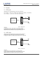
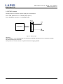
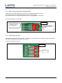
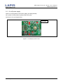
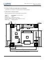
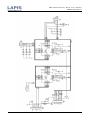
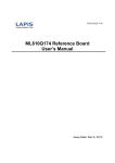
FEBL610Q304-01
ML610Q304 Reference Board
User’s Manual
st
1
Version : Issue date Dec.02, 2014
ML610Q304 Reference Board User’s Manual
FEBL610Q304RB-01
NOTES
No copying or reproduction of this document, in part or in whole, is permitted without the consent of LAPIS Semiconductor
Co., Ltd.
The content specified herein is subject to change for improvement without notice.
Examples of application circuits, circuit constants and any other information contained herein illustrate the standard usage
and operations of the Products. The peripheral conditions must be taken into account when designing circuits for mass
production.
Great care was taken in ensuring the accuracy of the information specified in this document. However, should you incur
any damage arising from any inaccuracy or misprint of such information, LAPIS Semiconductor shall bear no
responsibility for such damage.
The technical information specified herein is intended only to show the typical functions of and examples of application
circuits for the Products. LAPIS Semiconductor does not grant you, explicitly or implicitly, any license to use or exercise
intellectual property or other rights held by LAPIS Semiconductor and other parties. LAPIS Semiconductor shall bear no
responsibility whatsoever for any dispute arising from the use of such technical information.
The Products specified in this document are intended to be used with general-use electronic equipment or devices (such
as audio visual equipment, office-automation equipment, communication devices, electronic appliances and amusement
devices).
The Products specified in this document are not designed to be radiation tolerant.
While LAPIS Semiconductor always makes efforts to enhance the quality and reliability of its Products, a Product may fail
or malfunction for a variety of reasons.
Please be sure to implement in your equipment using the Products safety measures to guard against the possibility of
physical injury, fire or any other damage caused in the event of the failure of any Product, such as derating, redundancy,
fire control and fail-safe designs. LAPIS Semiconductor shall bear no responsibility whatsoever for your use of any
Product outside of the prescribed scope or not in accordance with the instruction manual.
The Products are not designed or manufactured to be used with any equipment, device or system which requires an
extremely high level of reliability the failure or malfunction of which may result in a direct threat to human life or create a
risk of human injury (such as a medical instrument, transportation equipment, aerospace machinery, nuclear-reactor
controller, fuel-controller or other safety device). LAPIS Semiconductor shall bear no responsibility in any way for use of
any of the Products for the above special purposes. If a Product is intended to be used for any such special purpose,
please contact a ROHM sales representative before purchasing.
If you intend to export or ship overseas any Product or technology specified herein that may be controlled under the
Foreign Exchange and the Foreign Trade Law, you will be required to obtain a license or permit under the Law.
Copyright 2014 LAPIS Semiconductor Co., Ltd.
2-4-8 Shinyokohama, Kouhoku-ku,
Yokohama 222-8575, Japan
http://www.lapis-semi.com/en/
FEBL610Q304-01
1
ML610Q304 Reference Board User’s Manual
FEBL610Q304RB-01
Preface
This user’s manual provides comprehensive explanation about ML610Q304 Reference Board.
Together with this manual, please also refer to the following documents.
■
ML610Q304 User’s Manual
The manual to explanation about ML610Q304
■
μEASE User’s Manual
The manual to explanation about μEASE / on-chip debugging tool
FEBL610Q304-01
2
ML610Q304 Reference Board User’s Manual
FEBL610Q304RB-01
1. Outline
1.1
Features
This reference board enables the customers to evaluate the functionalities of ML610Q304 and bears
several pads for mounting additional devices.
By using together another board called “μEASE (a On-chip Debug Emulator from Lapis)” & its bundled
software development tool, software development, debugging and Flash ROM writing are possible too.
It is possible to utilize this reference board without μEASE by simply connecting the power supply.
Please go through this manual when using this board.
1.1.1
Features of board
・ML610Q304 is mounted (or 28pin IC socket is mounted)
・Flash ROM programming and on-chip debugging are possibe (TEST0、TEST1_N pins are provided)
・High expandability – Micro’s pins are set on through-holes intended for connecting with other board(s)
・Power supply is selectable, either from μEASE from other board.
・Service pads are provided for mounting additional components that may be necessary to check / evaluate
Micro’s functionalities.
1.1.2
Specifications of board
* Please refer to p.5 “circuit diagram” for detailed connectivity for mounted components.
Mounted micro
Mounted
components
Pads for
additional componets
Other service pads
Drive voltage
Outer dimensions
FEBL610Q304-01
・ U1 / U2(mounted type / socket type): ML610Q304
・ PWR: Input power supply switching jumper(3pin pinheader & short pin)
・ VREF: VREF input pin(3pin pinheader & short pin)
・ SPEAKER: Speaker jack
・ R1-R3: Resistor for Light Emitting Diode(P20-P22)
・ P20-P22: Light Emitting Diode
・ CNUE: Connector (14 pin) for On-chip debug emulator
・ C1-C8: Capacitor for power supply(8pieces)
・ C9-C11: SA-ADC Capacitor for power supply line(3pieces)
・ CN1-CN3: Connector bads for other board(s)
( 6pin, 7pin, 12pin, 2.54mm pitch)
・ SP1-SP6: Lands for pouwer supply line
・ SP7-SP9: Non-resistance chips for connecting LED
・ SP10: SPVDD select pint for input power supply
・ UVDD、VDD、VSS、AIN0-AIN2
・ +2.0~+5.5V
・ 60.00 x 70.00 mm
3
ML610Q304 Reference Board User’s Manual
FEBL610Q304RB-01
1.2
Outlook
The photo of ML610Q304 Reference Board is as below Figure 1 & 2.
PWR
CNUE
SPEAKER
CN2
U1
mount
SPVDD
CN1
U2
socket
AIN0-AIN2
P20-P22
VREF
CN3
J
XXX
Q304
Figure 1. ML610Q304 Reference Board outlook
1pin
Figure 2. ML610Q304 Reference Board – Orientation of mounting IC
* Cautions)
Pleases set the IC on the board after turning the power off,
FEBL610Q304-01
in the correct orientation.
4
ML610Q304 Reference Board User’s Manual
FEBL610Q304RB-01
2.
Function
2.1
PWR jumper
PWR jumper is for selecting power source line for this board.
If from μEASE, please set to “uEASE” side of PWR jumper. (Capaity :+3.3V/100mA)
If from UVDD pin, please set to “USR” side of PWR jumper.
PWR
uE
CNUE
13pin
ML610Q304
VDD
USR
UVDD
Figure 3. PWR jumper
Cautions)
If PWR jumper is set to “USR” side for connecting to μEASE,
the customer’s set should be turned on after μEASE is connected.
μEASE should be put off after the user’s sytem is turned off.
2.2
VREF jumper
VREF jumper is for selecting the line for power supply to VREF pin.
If supply from VDD, VREF jumper should be set to ”VDD” side.
If supply from UVREF pin, VREF jumper should be set to “USR” side.
VREF
VDD
ML610Q304
VDD
VREF
USR
Figure 4
UVREF
VREF jumer
Cautions)
If VREF jumper is set to“USR”side for connecting μEASE,
the user’s system should be turned on after μEASE is connected.
μEASE should be put off after the user’s sytem is turned off.
FEBL610Q304-01
5
ML610Q304 Reference Board User’s Manual
FEBL610Q304RB-01
2.3 SPVDD Jumper
SPVDD jumper is to select the power supply line for SPVDD pin.
If from VDD, please set to”1” of SPVDD jumper (SP10)
If from SPVDD pin, please to “3” of SPVDD jumper.
SP10
1
ML610Q304
VDD
SPVDD
3
SPVDD
Figure 5. VREF jumper
Cautions)
When setting to “3” of SPVDD jumper for connecting to μEASE, please turn on the customer’s system
only after finishing the connection.
Also, please turn off the customer’s system first before stopping μEASE.
FEBL610Q304-01
6
ML610Q304 Reference Board User’s Manual
FEBL610Q304RB-01
2.4 When using sequential comparator ADC
Please connect to AIN0-AIN2 on the board to run the data through AD conversion.
If input from CN3 is not used, please input from the holes near CN3
Also, please add noise-reduction capacitor(s) C9-C11 as appropriate, if necessary.
See Figure 5 below as an example.
Top View
If no input from CN3,
please input directly
from these holes.
Put noise reduction
capacitors on these
holes.
Figure 6, An example of ADC (sequential comparator) AIN0-AIN2 mounting
2.5
If LED does not emit
P20-P22 pins enable direct drive of LED. As LED(s) are connected to non-resitance chip(s) on this board,
SP7-SP9 should be removed if LED is not driven.
See Figure 6 below for rerence.
Top View
Remove
Figure 7
FEBL610Q304-01
SP7-SP9 Pads example
7
ML610Q304 Reference Board User’s Manual
FEBL610Q304RB-01
2.6
Cut-off power supply
Please cut off the patterns of SP1/SP4 (VDD)、SP3/SP6 (SPVDD).
Also, please cut SP5 pattern if getting VDDL-VSS apart.
See Figure 7 for an example below.
Top View
Figure 8
FEBL610Q304-01
An example of power cut-off
8
ML610Q304 Reference Board User’s Manual
FEBL610Q304RB-01
3. User Interface
3.1 User Interface for ML610Q304 Reference Board
Following is the table of pin-out of CN1/CN2/CN3 for the ML610Q304 Reference Board
(ML610Q304 is mounted)
ML610Q304
PIN
Name
1
P22
2
P21
3
VSS
4
P20
5
P80
6
P81
7
TEST1_N
8
TEST0
9
P82
10
P83
11
RESET_N
12
SPP
13
SPM
14
(NC)
15
SPVSS
16
SPVDD
17
P84
18
P85
19
VSS
20
VDDL
21
VDD
22
P42/AIN2
23
P41/AIN1
24
P40/AIN0
25
VREF
26
P86
27
P87
28
NMI
FEBL610Q304-01
Table 1. ML610Q304 Reference Board CN1/CN2/CN3
ML610Q304 Reference Board
Remarks
User connector
PIN
CN1
1
Connecting also to LED
CN1
2
Connecting also to LED
CN1
3
CN1
4
Connecting also to LED
CN1
5
CN1
6
Connecting to μEASE connector
-
-
Connecting to μEASE connector
-
-
CN2
1
CN2
2
CN2
3
CN2
4
Connecting to speaker jack
CN2
5
Connecting to speaker jack
-
-
CN2
6
Connecting to VSS
CN2
7
Connecting to VDD
CN2
8
CN2
9
CN2
10
CN2
11
CN2
12
Switchable μEASE 3.3V ⇔ jumper
CN3
1
Input through-hole available
CN3
2
Input through-hole available
CN3
3
Input through-hole available
CN3
4
Switchable VDD ⇔ jumper
CN3
5
CN3
6
CN3
7
9
ML610Q304 Reference Board User’s Manual
FEBL610Q304RB-01
4. Cautions when using
(1) The contents of this manual, due to improvement of device and involved technologies,
may be changed with / without prenotice.
(2) Please read the ML610Q304 manual and μEASE manual when working with boards.
(3) On this board, Engineering Sample of ML610Q304 may be mounted.
For final cofirmation on electric characteristics, please do it with ML610Q304 from massproduction
and also on the customer’s board for massproduciton.
(4) We do not offer repair service for this board. The replacement board will be offered when
the failure is notified at early stage.
(5) Please CN2_3 pin (RESET_N) open when using μEASE.
(When preparing RESET_N signal on other board, please add jumper pin and leave it open)
(6) This board has patterns on the reverse side, so that please take care to avoid “short” with other board/
components conductive (particularly when the board is set over them.)
Use of any insulative materials inbetween, or applying protective sheet on the reverse-side pattern
or applying the rubber legs on the board to keep distance.
FEBL610Q304-01
10
ML610Q304 Reference Board User’s Manual
FEBL610Q304RB-01
5. Outline of reference board and circuit diagram
Specification & circuit diagram of reference boards are stated herein after.
5.1 Specification of reference board
Below is the basic specification of ML610Q304 Reference Board
● Dimesion
:Vertical 60mm × horizontal 70mm
●Layer
:two (2) layers
●Thickness
:1.6mm
●Conductor pitch :2 lines between the pins
●Conductor width:Powerline=0.3mm、signal line=0.15mm
●Rubber cap
:4 pieces (locations)
2.54
5.5
4-φ3.6
uE
13
C
1
14
USR
2
CNUE
SPEAKER
SPM
21
6
P81
7
22
P80
P20
1
28
VSS
P84
AIN2
AIN0
AIN1
15
P85
VSS
40
15
SPVDD
60
8
ML610Q304
14
8
SPP
SPVSS
14
P21
7
P22
▲
RESET_N
▲
P83
21
1
1
P82
CN1
CN2
1
PWR
VDD
VDDL
C
UVDD
12
USR
P20 P21 P22
28
25.4
22
NMI
P87
P86
UVREF
P40/AIN0
P41/AIN1
CN3
1
P42/AIN2
2.54
15.24
VREF
7
15.24
66.04
70
Figure 9
FEBL610Q304-01
Dimension of board (top view)
11
ML610Q304 Reference Board User’s Manual
FEBL610Q304RB-01
5.2 Circuit Diagram
Circuit diagram of ML610Q304 Reference Board is show on the next page.
FEBL610Q304-01
12
ML610Q304 Reference Board User’s Manual
FEBL610Q304RB-01
FEBL610Q304-01
13
ML610Q304 Reference Board User’s Manual
FEBL610Q304RB-01
Revision history
Page
Document No.
FEBL610Q304RB-01
FEBL610Q304-01
Issue date
2014.12.2
Contents of change
Before
After
–
–
st
1 version issued
14