1
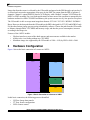
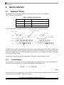
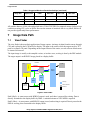
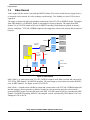
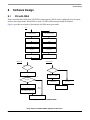
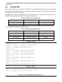
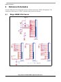
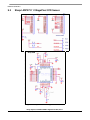
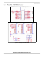
Freescale Semiconductor
Application Note
Document Number: AN2676
Rev. 1, 10/2005
Image Capture with MC9328MX21
by: Cliff Wong
1
Abstract
This document provides guidelines to implement image
capture applications using the CMOS Sensor Interface
Module (CSI) of the MC9328MX21 (i.MX21). Several
scenarios are analyzed, including the view finder, still
capture, and video conferencing. This application note
also includes supplementary information about the CSI
module and the CSI-PRP connection.
NOTE
The PRP settings defined in this application
note apply only to the MC9328MX21 with
the mask sets 0L92S and 1L92S.
2
Introduction
Image capture is one of the key features of the i.MX21
processor. Using the CSI module and the eMMA
Pre-processor (PRP), the user can easily build view
finder, still image capture, and video recording
applications.
© Freescale Semiconductor, Inc., 2005. All rights reserved.
Contents
1 Abstract . . . . . . . . . . . . . . . . . . . . . . . . . . . . . . . . .1
2 Introduction . . . . . . . . . . . . . . . . . . . . . . . . . . . . .1
3 Hardware Configuration . . . . . . . . . . . . . . . . . . .2
4 Initialization . . . . . . . . . . . . . . . . . . . . . . . . . . . . . .3
5 Sensor Interface . . . . . . . . . . . . . . . . . . . . . . . . . .4
6 Bayer Statistics . . . . . . . . . . . . . . . . . . . . . . . . . .6
7 Image Data Path . . . . . . . . . . . . . . . . . . . . . . . . . .8
8 Software Design . . . . . . . . . . . . . . . . . . . . . . . . .11
9 Reference Schematics . . . . . . . . . . . . . . . . . . . .16
10References . . . . . . . . . . . . . . . . . . . . . . . . . . . . .21
11Revision History . . . . . . . . . . . . . . . . . . . . . . . . .21
Hardware Configuration
Image data from the sensor is collected by the CSI module and passed to the PRP through a private bus. It
is resized and converted to appropriate color space by the PRP. The output from the PRP is split into 2
channels. Channel 1 outputs RGB565 data for LCD display; while Channel 2 outputs YUV420 data for
MPEG or JPEG encoding. For view finder applications, because most of the operation is managed by the
hardware and involves little CPU MIPS and memory, the system can run at a very low speed to save power.
The CSI module is able to accept most image data formats: YUV444 / YUV422 / RGB565 / RGB888 /
Bayer. However, the data path from the CSI module to the PRP is designed for YUV422 and RGB565 only.
For the other formats, image pre-processing is handled by software. Choose the path from the CSI module
to Memory through DMA. CPU MIPS and memory usage, and thus the power consumption, increases
according to the image size.
Features of the i.MX21 include:
• Glueless interface to most of the dumb sensors and smart sensors available in the market
• Ability to do view finding without any CPU MIPS
• Maximum image size supported by the CSI module is 2560 × 1920, by PRP is 2048 × 2048
3
Hardware Configuration
Figure 1 shows the basic connection of a sensor to i.MX21.
OSC
MCLK
Sensor
CSI
VSYNC
HSYNC
PIXCLK
D[7..0]
I2C_SCL
I2C_SDA
I2C
RESET
GPIO
STANDBY
Figure 1. Basic Connection of a Sensor to i.MX21
In this basic connection, the following ports are identified:
• CSI Port: Image data transfer
• I2C Port: Sensor configuration
• GPIO: Sensor control
Image Capture with MC9328MX21 Application Note, Rev. 1
2
Freescale Semiconductor
Initialization
The i.MX21 CSI module has an 8-bit input port. If the sensor has more than 8-bit data, connect the most
significant bits to i.MX21, and leave the rest of the bits floating.
Sensors are usually controlled by the I2C port as slave devices. The low level protocol is I2C, while the
high level protocol is specific to the sensor. For more information, see the user manual of the particular
sensor being used.
Some of the basic sensor controls, for example, reset and standby, are done through hardware signals.
These can be implemented with GPIO ports for i.MX21.
A sensor master clock can be provided by i.MX21, or by an external oscillator.
4
4.1
Initialization
Power Saving
The clock trees connected to the CSI, I2C, DMA, PRP, and LCDC module, shown in Table 1, are turned
off by default in the Clock Control Module for power saving purpose. The clock must be enabled first.
Table 1. Clock Trees for the CSI, I2C, DMA, PRP, and LCDC Module
4.2
Module
Peripheral Clock Control Register
Enable Bit
CSI
PCCR0
31
I2C
PCCR0
12
DMA
PCCR0
30, 23
PRP
PCCR0
27, 15
LCDC
PCCR0
26
IO Port
The pin assignments for the CSI, I2C, and LCDC modules, shown in Table 2, are set to GPIO ports by
default. They must be enabled for functional pins first.
Table 2. Pin Outs for CSI, I2C, and LCDC Modules
Module
Port
CSI
PB[21:10]
I2C
PD[18:17]
LCDC
PA[31:5]
Image Capture with MC9328MX21 Application Note, Rev. 1
Freescale Semiconductor
3
Sensor Interface
5
5.1
Sensor Interface
Traditional Timing
The traditional timing interface employs 3 clock signals and an 8-bit or 10-bit data bus.
Table 3 shows the clock signals.
Table 3. Traditional Timing Interface
Signal Name
Abbreviation
Meaning
Vertical Sync
VSYNC
Start of frame (SOF)
Horizontal Sync
HSYNC
Start of line and validate pixel clock
Pixel Clock
PIXCLK
Carry pixel data
The basic operation of traditional timing is Gated-Clock Mode as shown in Figure 2.
Figure 2. Gated-Clock Mode Timing
The start of frame (SOF) interrupt is generated upon the rising or falling edge of the VSYNC. HSYNC and
PIXCLK are internally AND-ed together to provide the valid pixel clock signal. The polarity of HSYNC
can be active-high or active-low. Data is latched to the FIFO on every valid pixel clock edge. Valid edges
can be either rising or falling.
Configuration of the timing details is through the CSI module Control Register 1 (CR1).
5.1.1
Clock Scheme
The CSI module is designed to accept input signals that are asynchronous to the system clock (HCLK).
Synchronization is done internally as long as the following relationship holds:
HCLK ≥ 2 × PIXCLK
Eqn. 1
Sensors usually run on a single master clock (MCLK) and use it to divide out the pixel clock. MCLK can
be taken from the CSI module or other clock source.
Image Capture with MC9328MX21 Application Note, Rev. 1
4
Freescale Semiconductor
Sensor Interface
5.1.2
DMA Synchronization Issue
When using DMA in non-repeat mode for the CSI module, synchronization is an important issue.
Consider the timing of VSYNC as shown in Figure 3.
SOF
VSYNC
Valid Data
D[7..0]
Latency
Figure 3. Timing of VSYNC
Upon the arrival of SOF, an interrupt triggers, which forces the software to run in the ISR register of the
CSI module. DMA is then enabled.
To avoid loss of data, DMA must be enabled within the latency shown in Figure 3. The latency is
determined by the timing of the sensor, usually from a few tens of MCLK to a few thousands of MCLK.
For non-real time operating systems for example, Linux, the latency of the interrupt service routine is not
guaranteed. There may be an uncertain delay inserted before DMA is enabled. This results in data loss.
The problem becomes more serious as the system load increases.
The loss sync problem is localized to one frame and does not propagate to the subsequent frames. Every
frame is synchronized with its own SOF. Each has an equal chance of loss sync.
5.2
CCIR Progressive Mode
Most smart sensors support CCIR656 encoding. Markers indicating the start of active video (SAV) and end
of active video (EAV) are embedded in the data stream. Only PIXCLK and data bus are used. VSYNC and
HSYNC are no longer required. The CCIR decoder should be able to reconstruct the VSYNC and HSYNC
from the embedded timing.
Figure 4 illustrates the general timing of a single line:
Figure 4. General Timing of a Single Line
However, the CCIR656 standard was originally designed for interlaced video. For the progressive mode,
which is the subject of concern with CMOS sensors, there are no strict definitions for start of frame (SOF)
and end of frame (EOF). Different manufacturers can adapt the spec to their own, so embedded VSYNC
markers behave slightly differently from each other. To accommodate different sensors, the CSI module is
Image Capture with MC9328MX21 Application Note, Rev. 1
Freescale Semiconductor
5
Bayer Statistics
designed to work with both embedded (or internal) VSYNC and external VSYNC. The latter case is
suitable only for those sensors that provide a VSYNC signal.
In most cases, external VSYNC mode is more useful.
CCIR progressive mode is enabled through CSI Control Register 1(CR1).
6
Bayer Statistics
Bayer statistics provide the reference for camera control and basic image pre-processing. In the CSI
module, a hardware statistics block is included to help software with exposure control, focus control, and
white balance control.
The hardware accepts only Bayer data format, which is the one output from a raw image sensor. Smart
sensors that output RGB or YUV are not supported. Indeed, smart sensors do camera control and image
pre-processing with their own hardware before data is sent out.
All configurations on the Bayer statistics block are done through CSI Control Register 2.
6.1
White Balance
According to the Grey World model, to give a correct white color, the average (or sum) of every color in
an image should be equal. This is done by applying multipliers on 2 of the 3 primary color pixels. Usually
the green pixel is taken as the reference and used to generate the coefficient for blue and red.
δ Blue
∑g
=
∑b
i
i
i
i
bi' = δ Blue × bi
δ Re d
∑g
=
∑r
i
i
i
i
ri ' = δ Re d × ri
Eqn. 2
6.2
Exposure Control
Exposure time is adjusted to a value that produces the greatest dynamic range with minimum noise level.
The adjustment is made at regular time intervals until the mean value of a specific color hits a target value.
For details, see the data sheet of the particular sensor.
6.3
Statistic Block Operation
The Bayer statistics are operated on image blocks. The image is divided into several square blocks; each
block has one set of statistics data output. One set of statistics includes Sum of Red, Sum of Green, Sum
of Blue, and Sum of Absolute Green Data (SOAD). Sum of Red, Green, and Blue are used in white balance
and exposure control, while SOAD is only used in focus control.
Image Capture with MC9328MX21 Application Note, Rev. 1
6
Freescale Semiconductor
Bayer Statistics
The image block size is pre-defined according to different live view resolutions (LVRM). The number of
blocks per row and per column is also pre-defined, which limits the aspect ratio (image width ÷ image
height) that is supported. To fit different image sizes, a line-skipping scheme is employed. Adjacent blocks
are separated by skipped lines. The number of skipped lines is programmable through register CR2.
Horizontal and vertical line skipping can be programmed independently. The rule is that sum of block size
plus the number of lines skipped must be equal to the image size.
H img = ∑ ( H block + H SC )
i
Vimg = ∑ (Vblock + VSC )
j
Eqn. 3
The maximum supported resolution is equal to the maximum block size plus the skipped lines. For
LVRM = 0, HSC = 256, VSC = 256, the maximum resolution is 2560 × 1920.
Using the VGA case as an example, based on LVRM = 0, and HSC = VSC = 16, we have the results shown
in Figure 5.
HSC = 16
640
VSC = 16
480
64
64
Figure 5. Maximum Resolution Supported
Another choice for VGA can be LVRM = 1, and HSC = VSC = 24, and so on.
Table 4 shows suggested settings for different image sizes.
Table 4. Suggested Maximum Resolution Settings
Image Size
Aspect Ratio
LVRM
Block Size
HSC / VSC
CR2 Value
352 x 288
11 : 9
4
40 x 40
4/8
0x840703
640 x 480
4:3
0
64 x 64
16 / 16
0x800F0F
1024 x 768
4: 3
0
64 x 64
64 / 64
0x803F3F
Image Capture with MC9328MX21 Application Note, Rev. 1
Freescale Semiconductor
7
Image Data Path
Table 4. Suggested Maximum Resolution Settings (continued)
Image Size
Aspect Ratio
LVRM
Block Size
HSC / VSC
CR2 Value
1280 x 960
4:3
0
64 x 64
96 / 96
0x805F5F
1536 x 1024
3:2
3
64 x 64
192 / 192
0x83BFBF
1280 x 1024
5:4
Not Supported
All statistics data are 16-bit wide and packed into a 32-bit STAT FIFO for temporal storage. Software can
read this out using CPU cycles or DMA. Because the amount of statistical data is very small, DMA will
not provide significantly better performance.
7
7.1
Image Data Path
View Finder
The view finder is the most basic application of image capture. An image is taken from the sensor, through
CSI, and is placed in the LCD buffer for display. The input is the sensor, while the output can be a TFT
panel or a smart LCD panel. Depending on the output format of the sensor, several software blocks must
be inserted in between.
The input image is usually a sub-sampled version, or in other cases, resizing is done by the PRP module.
The target output is an RGB565 image placed in a display buffer.
RGB565
LCDC
RXFIFO
CSI
STAT FIFO
RGB565
YUV422
Bayer
YUV444
RGB888
Line
Buffer
Camera
Control
RGB565
PRP
RGB565
Display
Buffer
SLCDC
Frame
Buffer
Memory
Color
Proc
MX21 Module
Software
Figure 6. View Finder
Path 1(Red)—A smart sensor with RGB565 output is used, and, there is no need for resizing. Data is
directly forwarded to the display buffer by DMA. A minimal amount of CPU MIPS is required.
Path 2 (Blue)—A smart sensor with RGB565 output is used, and resizing is required. Data is passed to the
PRP for resizing, then forwarded to the display buffer.
Image Capture with MC9328MX21 Application Note, Rev. 1
8
Freescale Semiconductor
Image Data Path
Path 3 (Blue)—A smart sensor with YUV422 output is used. Data is passed to the PRP for color
conversion and resizing, then forwarded to display buffer.
Path 4 (Green)—A dumb sensor with Bayer output and a smart sensor with RGB888 / YUV444 output fall
into this category. Data is passed to a software routine for color processing and color conversion. The
output is fed into the PRP via a frame buffer for resizing, and then forwarded to the display buffer. A
maximum amount of CPU power is consumed.
7.2
Still Capture
In still capture, the image is captured frame by frame. A high quality image is obtained after the whole
chain of color processing, and that image is then converted to YUV420 for JPEG encoding.
The image is captured in full resolution in either YUV422 or RGB565 format. The output from PRP
channel 1 is in RGB565 format, a sub-sampled version for display. The output from PRP channel 2 is in
YUV420 format in full size for JPEG encoding. Both outputs are placed in memory.
Sensors with Bayer, YUV444, or RGB888 output are also supported, with several software blocks inserted
in between.
YUV422
RGB565
RGB565
PRP
Frame
Buffer
RXFIFO
CSI
Bayer
YUV444
RGB888
Camera
Control
SLCDC
RGB565
YUV420
STAT FIFO
Line
Buffer
LCDC
Frame
Buffer
Frame
Buffer
JPEG
Enc
Storage
Memory
Color
Proc
MX21 Module
Software
Figure 7. Still Capture
Path 1 (Red)—A smart sensor with YUV422 and RGB565 output is used. A full-sized image is converted
to YUV420 by PRP channel 2 for compression by a software JPEG encoder. The same image is resized
and converted to RGB565 by PRP channel 1 for preview.
Path 2 (Blue)—A dumb sensor with Bayer output and a smart sensor with YUV444 / RGB888 output fall
into this category. Data is passed to a software routine for color processing and color conversion to
generate RGB565 output, and this is fed back to the PRP, via a frame buffer, for resizing and further color
conversion. A full-sized image is converted to YUV420 by PRP channel 2 for compression by a software
JPEG encoder. The same image is resized and converted to RGB565 by PRP channel 1 for preview.
Image Capture with MC9328MX21 Application Note, Rev. 1
Freescale Semiconductor
9
Image Data Path
7.3
Video Record
Video captured by the sensor is encoded into MPEG4 format. This can be stored in mass storage devices,
or streamed out by network for video exchange (conferencing). View finding on a local LCD screen is
supported.
The image is captured in full or sub-sampled resolution in either YUV422 or RGB565 format. The output
from PRP channel 1 is in RGB565 format, a sub-sampled version for display. The output from PRP
channel 2 is in YUV420 format in full size for MPEG4 encoding. Both outputs are placed in memory.
Sensors with Bayer / YUV444 / RGB888 output are also supported, with several software blocks inserted
between.
LCDC
Frame
Buffer
RGB565
YUV422
RGB565
CSI
PRP
Frame
Buffer
RXFIFO
YUV420
SLCDC
STAT FIFO
Bayer
YUV444
RGB888
Line
Buffer
MPEG4
Encoder
RGB565
Frame
Buffer
Memory
MX21 Module
Software
Camera
Control
Color
Proc
Statistics
Figure 8. Video Record
Path 1 (Blue)—A smart sensor with YUV422 / RGB565 output is used. Data is resized and converted to
YUV420 by PRP channel 2 for MPEG4 encoding. The same image is resized and converted to RGB565
color by PRP channel 1 for display on an LCD or SLCD.
Path 2 (Red)—A dumb sensor with Bayer output and a smart sensor with YUV444 / RGB888 output fall
into this category. Data is passed to a software routine for color processing and color conversion to
generate RGB565 output. It is then fed back to the PRP. YUV420 output of full size is produced by PRP
channel 2 for MPEG4 encoding. RGB565, sub-sampled version, is produced by PRP channel 1 for view
finding on LCD or SLCD.
Image Capture with MC9328MX21 Application Note, Rev. 1
10
Freescale Semiconductor
Software Design
8
8.1
Software Design
CSI with DMA
Data is transferred by DMA from CSI FIFO to main memory. DMA can be configured to run in repeat
mode or non-repeat mode. When DMA is used, CSI FIFO-full interrupts should be disabled.
Figure 9 provides an example of pseudocode for DMA non-repeat mode.
Init
CSI Port Enable
CSI Timing Config
Enable HCLK
Enable sync FIFO clear
Enable MCLK
Enable SOF Interrupt
Init I2C
Init DMA
Init Sensor
Return
ISR for CSI
ISR for DMA
SOF_INT = ‘1’?
DISR = ‘1’?
N
Y
Write ‘1’ to SOF_INT
Write ‘1’ to DISR
N
DMA complete
flag set?
Set DMA
complete flag
Y
Set DMA
error flag
Enable DMA channel
Miss
Frame
Return
Clear DMA complete flag
Return
Figure 9. DMA Non-Repeat Mode
Image Capture with MC9328MX21 Application Note, Rev. 1
Freescale Semiconductor
11
Software Design
8.2
CSI with PRP
Data is transferred by a private bus from CSI FIFO to the eMMA-PRP module. After the bus is enabled,
the image data is forwarded to the PRP continuously, and the path to DMA is switched off by internal logic.
No CSI FIFO interrupts are generated.
The PRP module is able to accept RGB565 or YUV422 data from CSI. Data formats are shown in Table 5.
RGB565 data is Big-endian while YUV422 data is Little-endian.
Table 5. Data Formats Accepted by PRP
Data Format
Endian
Swap16
RGB565
Big
Enable
YUV422
Little
Disable
Table 6 shows VGA output in RGB565 format.
Table 6. VGA Output in RGB565 Format
Signal
Resolution
Color Space
CSI Input
Traditional Timing VGA
RGB565
CSI Output / PRP Input
VGA
RGB565
PRP Ch1 Output
QVGA (Stride to 240x240)
RGB565
PRP Ch2 Output
QVGA
YUV420
Example 1. CSI Init
//module init
* (uint32_t *)GPIOB_GIUS &= ~0x3FFC00;//disable GPIO PB[21..10]
* (uint32_t *)CRM_PCCR0 |= 0x80000000;//HCLK clock enable
*(uint32_t *) CSI_CSICR1 = 0x0;//register clear
*(uint32_t *) CSI_CSICR1 |= 0x0200;//MCLK = HCLK / 2
//timing control
*(uint32_t *) CSI_CSICR1 |= 0x20000;//SOF rising edge
*(uint32_t *) CSI_CSICR1 |= 0x10000;//SOF INT enable
*(uint32_t *) CSI_CSICR1 |= 0x2;//latch on rising edge
*(uint32_t *) CSI_CSICR1 |= 0x10;//gated clock mode
*(uint32_t *) CSI_CSICR1 |= 0x800;//hsync active high
//FIFO control
*(uint32_t *) CSI_CSICR1 |= 0x100;//sync FIFO clear
*(uint32_t *) CSI_CSICR1 |= 0x100000;//RXFF level = 16
//data manipulation
*(uint32_t *) CSI_CSICR1 |= 0x80000000;//swap16 enable
*(uint32_t *) CSI_CSICR1 |= 0x80;//big endian
//PRP i/f control
*(uint32_t *) CSI_CSICR1 |= 0x10000000;//PRP i/f enable
Example 2. PRP Init
//Module init
*(uint32_t *)CRM_PCCR0 |= 0x8008000;//Clock enable for PRP
*(uint32_t *)EMMA_PRP_CNTL |= 0x10000;//PRP reset
Image Capture with MC9328MX21 Application Note, Rev. 1
12
Freescale Semiconductor
Software Design
//common control
*(uint32_t *)EMMA_PRP_CNTL = 0x0008F24E;//LOOP mode
//matrix B0 (YUV2RGB),
matrix B0 (RGB2YUV)
//RGB565 => RGB565 (ch1), YUV420 (ch2)
//CSI i/f enable
//ch1, ch2 enable
*(uint32_t *)EMMA_PRP_CNTL |= 0x8000000;//bug fix
*(uint32_t *)EMMA_PRP_RSIZE_CTRL = 0x40;//MAIN resize = 2:1, CSC
resize = 1:1
*(uint32_t *)EMMA_PRP_INTRCTRL = 0x00000000;//disable interrupt
//source control
//*(uint32_t *)EMMA_PRP_SY_PTR;//source ptr : NOT used with CSI
*(uint32_t *)EMMA_PRP_SPIX_FMT = 0x2CA00565;//RGB565 input
*(uint32_t *)EMMA_PRP_SFRM_SIZE = 0x028001E0;//source = 640 x 480
//*(uint32_t *)EMMA_PRP_SLIN_STRID;//source line stride : NOT
used with CSI
//ch1 (RGB) dest control
*(uint32_t *)EMMA_PRP_DRGB1_PTR = rgb;//output buf1
*(uint32_t *)EMMA_PRP_DRGB2_PTR = rgb;//output buf2
*(uint32_t *)EMMA_PRP_DISIZE_CH1 = 0x00F000F0;//dest size = 240 x 240
*(uint32_t *)EMMA_PRP_DPIX_FMT = 0x2CA00565;//RGB565 output
*(uint32_t *)EMMA_PRP_DLST_CH1 = 0x000001E0;//dest line stride = 240
//ch2 (YUV) dest control
*(uint32_t *)EMMA_PRP_DY_PTR = y;//output buf1
*(uint32_t *)EMMA_PRP_DCB_PTR = u;
*(uint32_t *)EMMA_PRP_DCR_PTR = v;
*(uint32_t *)EMMA_PRP_SY_PTR = y;//output buf2 (re-used in
LOOP mode)
*(uint32_t
*(uint32_t
*(uint32_t
*(uint32_t
*)EMMA_PRP_SCB_PTR = u;
*)EMMA_PRP_SCR_PTR = v;
*)EMMA_PRP_DISIZE_CH2 = 0x000000F0;//dest image height = 240
*)EMMA_PRP_CNTL |= 0x1;//PRP enable
Table 7 shows VGA output in YUV422 format.
Table 7. VGA Output in YUV422 Format
Signal
Resolution
Color Space
CSI Input
CCIR VGA
YUV422
CSI Output / PRP Input
VGA
YUV422
PRP Ch1 Output
PRP Ch2 Output
QVGA (Stride to 240
× 240)
QVGA
RGB565
YUV420
Image Capture with MC9328MX21 Application Note, Rev. 1
Freescale Semiconductor
13
Software Design
Example 3. CSI Init
//module init
* (uint32_t *)GPIOB_GIUS &= ~0x3FFC00;
* (uint32_t *)CRM_PCCR0 |= 0x80000000;
*(uint32_t *) CSI_CSICR1 = 0x0;
*(uint32_t *) CSI_CSICR1 |= 0x0200;
//CCIR control
*(uint32_t *) CSI_CSICR1 |= 0x400;
*(uint32_t *) CSI_CSICR1 |= 0x8000000;
*(uint32_t *) CSI_CSICR1 |= 0x40000000;
//timing control
*(uint32_t *) CSI_CSICR1 |= 0x10000;
*(uint32_t *) CSI_CSICR1 |= 0x2;
//FIFO control
*(uint32_t *) CSI_CSICR1 |= 0x100;
*(uint32_t *) CSI_CSICR1 |= 0x100000;
//PRP i/f control
*(uint32_t *) CSI_CSICR1 |= 0x10000000;
//disable GPIO PB[21..10]
//HCLK clock enable
//register clear
//MCLK = HCLK / 2
//CCIR mode enable
//CCIR interlace mode
//external VSYNC
//SOF INT enable
//latch on rising edge
//sync FIFO clear
//RXFF level = 16
//PRP i/f enable
Example 4. PRP Init
//Module init
*(uint32_t *)CRM_PCCR0 |= 0x8008000;
*(uint32_t *)EMMA_PRP_CNTL |= 0x10000;
//common control
*(uint32_t *)EMMA_PRP_CNTL = 0x0008323E;
//Clock enable for PRP
//PRP reset
//LOOP mode
//matrix A1 (YUV2RGB), matrix B0 (RGB2YUV)
//YUV422 => RGB565 (ch1), YUV420 (ch2)
//CSI i/f enable
//ch1, ch2 enable
*(uint32_t *)EMMA_PRP_CNTL |= 0x8000000;
//bug fix
*(uint32_t *)EMMA_PRP_RSIZE_CTRL = 0x40;
//MAIN ratio 2:1, CSC resize = 1:1
*(uint32_t *)EMMA_PRP_INTRCTRL = 0x00000000; //disable interrupt
//source control
//*(uint32_t *)EMMA_PRP_SY_PTR;
//source ptr : NOT used with CSI
*(uint32_t *)EMMA_PRP_SPIX_FMT = 0x03080888; //YUV422 input, UYVY...
*(uint32_t *)EMMA_PRP_SFRM_SIZE = 0x028001E0;//source = 640 x 480
//*(uint32_t *)EMMA_PRP_SLIN_STRID;
//source line stride : NOT used with CSI
//ch1 (RGB) dest control
*(uint32_t *)EMMA_PRP_DRGB1_PTR = rgb;
//output buf1
*(uint32_t *)EMMA_PRP_DRGB2_PTR = rgb;
//output buf2
*(uint32_t *)EMMA_PRP_DISIZE_CH1 = 0x00F000F0;//dest size = 240 x 240
*(uint32_t *)EMMA_PRP_DPIX_FMT = 0x2CA00565; //RGB565 output
*(uint32_t *)EMMA_PRP_DLST_CH1 = 0x000001E0; //dest line stride = 240
//ch2 (YUV) dest control
*(uint32_t *)EMMA_PRP_DY_PTR = y;
//output buf1
*(uint32_t *)EMMA_PRP_DCB_PTR = u;
*(uint32_t *)EMMA_PRP_DCR_PTR = v;
*(uint32_t *)EMMA_PRP_SY_PTR = y;
//output buf2 (re-used in LOOP mode)
*(uint32_t *)EMMA_PRP_SCB_PTR = u;
*(uint32_t *)EMMA_PRP_SCR_PTR = v;
*(uint32_t *)EMMA_PRP_DISIZE_CH2 = 0x000000F0;//dest image height = 240
*(uint32_t *)EMMA_PRP_CNTL |= 0x1;
8.3
//PRP enable
Reference Settings for PRP
Table 8 and Table 9 show example settings for PRP with CSI input.
Image Capture with MC9328MX21 Application Note, Rev. 1
14
Freescale Semiconductor
Software Design
Table 8. Case Definitions
CSI Output / PRP Input
Channel 1 Output
Channel 2 Output
Case
Resolution
Format
Resolution
Format
Resolution
Format
1
CIF
RGB565
CIF
RGB565
CIF
YUV420
2
CIF
RGB565
QCIF
RGB565
CIF
YUV420
3
CIF
YUV422
CIF
RGB565
CIF
YUV420
4
CIF
YUV422
QCIF
RGB565
CIF
YUV420
5
VGA
RGB565
QVGA
RGB565
QVGA
YUV420
6
VGA
RGB565
QQVGA
RGB565
QVGA
YUV420
7
VGA
YUV422
QVGA
RGB565
QVGA
YUV420
8
VGA
YUV422
QQVGA
RGB565
QVGA
YUV420
9
QVGA
RGB565
QVGA
RGB565
QVGA
YUV420
10
QVGA
RGB565
QQVGA
RGB565
QVGA
YUV420
11
QVGA
YUV422
QVGA
RGB565
QVGA
YUV420
12
QVGA
YUV422
QQVGA
RGB565
QVGA
YUV420
Table 9. PRP Register Settings
Common Control
Case
PRP_CNTL
Source Control
Channel 1 Control
Channel 2 Control
PRP_RSIZE PRP_SPIX_ PRP_SFR_ PRP_DISIZE_ PRP_DPIX_ PRP_DLST_
_CTRL
FMT
SIZE
CH1
FMT
CH1
PRP_DISIZE_
CH2
1
0x0008F24E 0x00000000 0x2CA00565 0x01600120 0x00F00120 0x2CA00565 0x000001E0
0x00000120
2
0x0008F24E 0x00000009 0x2CA00565 0x01600120 0x00B00090 0x2CA00565 0x000001E0
0x00000120
3
0x0008323E 0x00000000 0x03080888 0x01600120 0x00F00120 0x2CA00565 0x000001E0
0x00000120
4
0x0008323E 0x00000009 0x03080888 0x01600120 0x00B00090 0x2CA00565 0x000001E0
0x00000120
5
0x0008F24E 0x00000040 0x2CA00565 0x028001E0 0x00F000F0 0x2CA00565 0x000001E0
0x000000F0
6
0x0008F24E 0x00000049 0x2CA00565 0x028001E0 0x00F000F0 0x2CA00565 0x000001E0
0x000000F0
7
0x0008323E 0x00000040 0x03080888 0x028001E0 0x00F000F0 0x2CA00565 0x000001E0
0x000000F0
8
0x0008323E 0x00000049 0x03080888 0x028001E0 0x00A00078 0x2CA00565 0x000001E0
0x000000F0
9
0x0008F24E 0x00000000 0x2CA00565 0x014000F0 0x00F000F0 0x2CA00565 0x000001E0
0x000000F0
10
0x0008F24E 0x00000009 0x2CA00565 0x014000F0 0x00A00078 0x2CA00565 0x000001E0
0x000000F0
11
0x0008323E 0x00000000 0x03080888 0x014000F0 0x00F000F0 0x2CA00565 0x000001E0
0x000000F0
12
0x0008323E 0x00000009 0x03080888 0x014000F0 0x00A00078 0x2CA00565 0x000001E0
0x000000F0
NOTE
For channel 1, to fit the view finder output on a 240 × 320 screen, those with
output width greater than 240 are strided to 240. These include CIF, VGA
and QVGA. The output width can be restored to the expected one by setting
the PRP Destination Channel-1 Line Stride Register.
Image Capture with MC9328MX21 Application Note, Rev. 1
Freescale Semiconductor
15
Reference Schematics
9
Reference Schematics
Several CMOS and CCD sensors have been (or will be) tested on the i.MX21 EVB platform. The
connection of the sensors to i.MX21 is shown in this section for reference.
9.1
iMagic IM8803 VGA Sensor
Figure 10. iMagic IMM8803 VGA Sensor
Image Capture with MC9328MX21 Application Note, Rev. 1
16
Freescale Semiconductor
Reference Schematics
9.2
OmniVision OV9640 1.3MegaPixel Sensor
OV9640 Socket
CSI Connector
Figure 11. OmniVision OV9640 1.3MegaPixel Sensor
Image Capture with MC9328MX21 Application Note, Rev. 1
Freescale Semiconductor
17
Reference Schematics
9.3
Sharp LZ0P3721 1.1MegaPixel CCD Sensor
Sharp CCD
Figure 12. Sharp LZ0P3721 1.1MegaPixel CCD Sensor
Image Capture with MC9328MX21 Application Note, Rev. 1
18
Freescale Semiconductor
Reference Schematics
9.4
TransChip TC5740 VGA Sensor
P5KS 24 pins Header
CSI Connector
Figure 13. TransChip TC5740 VGA Sensor
Image Capture with MC9328MX21 Application Note, Rev. 1
Freescale Semiconductor
19
References
10 References
The following documents can be used for additional information:
1. MC9328MX21 Applications Processor Reference Manual
(order number: MC9328MX21RM)
For this and other technical documents about the i.MX21 products, go to www.freescale.com/imx.
11 Revision History
This revision is for the purpose of applying the Freescale template and does not include technical content
changes.
Image Capture with MC9328MX21 Application Note, Rev. 1
20
Freescale Semiconductor
NOTES
Image Capture with MC9328MX21 Application Note, Rev. 1
Freescale Semiconductor
21
How to Reach Us:
Home Page:
www.freescale.com
E-mail:
[email protected]
USA/Europe or Locations Not Listed:
Freescale Semiconductor
Technical Information Center, CH370
1300 N. Alma School Road
Chandler, Arizona 85224
+1-800-521-6274 or +1-480-768-2130
[email protected]
Europe, Middle East, and Africa:
Freescale Halbleiter Deutschland GmbH
Technical Information Center
Schatzbogen 7
81829 Muenchen, Germany
+44 1296 380 456 (English)
+46 8 52200080 (English)
+49 89 92103 559 (German)
+33 1 69 35 48 48 (French)
[email protected]
Japan:
Freescale Semiconductor Japan Ltd.
Headquarters
ARCO Tower 15F
1-8-1, Shimo-Meguro, Meguro-ku,
Tokyo 153-0064, Japan
0120 191014 or +81 3 5437 9125
[email protected]
Asia/Pacific:
Freescale Semiconductor Hong Kong Ltd.
Technical Information Center
2 Dai King Street
Tai Po Industrial Estate
Tai Po, N.T., Hong Kong
+800 2666 8080
[email protected]
For Literature Requests Only:
Freescale Semiconductor Literature Distribution Center
P.O. Box 5405
Denver, Colorado 80217
1-800-521-6274 or 303-675-2140
Fax: 303-675-2150
[email protected]
Document Number: AN2676
Rev. 1
10/2005
Information in this document is provided solely to enable system and software implementers to use
Freescale Semiconductor products. There are no express or implied copyright licenses granted
hereunder to design or fabricate any integrated circuits or integrated circuits based on the information
in this document.
Freescale Semiconductor reserves the right to make changes without further notice to any products
herein. Freescale Semiconductor makes no warranty, representation or guarantee regarding the
suitability of its products for any particular purpose, nor does Freescale Semiconductor assume any
liability arising out of the application or use of any product or circuit, and specifically disclaims any
and all liability, including without limitation consequential or incidental damages. “Typical” parameters
that may be provided in Freescale Semiconductor data sheets and/or specifications can and do vary
in different applications and actual performance may vary over time. All operating parameters,
including “Typicals”, must be validated for each customer application by customer’s technical experts.
Freescale Semiconductor does not convey any license under its patent rights nor the rights of others.
Freescale Semiconductor products are not designed, intended, or authorized for use as components
in systems intended for surgical implant into the body, or other applications intended to support or
sustain life, or for any other application in which the failure of the Freescale Semiconductor product
could create a situation where personal injury or death may occur. Should Buyer purchase or use
Freescale Semiconductor products for any such unintended or unauthorized application, Buyer shall
indemnify and hold Freescale Semiconductor and its officers, employees, subsidiaries, affiliates, and
distributors harmless against all claims, costs, damages, and expenses, and reasonable attorney
fees arising out of, directly or indirectly, any claim of personal injury or death associated with such
unintended or unauthorized use, even if such claim alleges that Freescale Semiconductor was
negligent regarding the design or manufacture of the part.
Freescale™ and the Freescale logo are trademarks of Freescale Semiconductor, Inc. ARM and the
ARM Powered Logo are registered trademarks of ARM Limited. All other product or service names
are the property of their respective owners.
© Freescale Semiconductor, Inc. 2005. All rights reserved.