1
SIDSA
3.
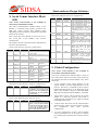
Command word status
2-wire Register
Interpretation
011x 1001
command is being sent
000x 1101
Arbitration lost.
Changed to slave mode
000x 0101
Slave device not addressed
(only in slave device)
11xx 1101
Acknowledge error.
No device addressed
11xx 1001
4.
Command successfully
transmitted and a device is
addressed
Transmission status
2-wire Register
Interpretation
0x1x 1001
TX/RX in progress
0x01 1101
TX error (‘false zero’sent)
(only in transmitter)
5.
1xxx 1001
Transmission completed
1xxx 1101
Acknowledge bit error
Semiconductor Design Solutions
• SCI boot sequence: the Serial Communication is
disabled and the 8051 serial interface is used. Two
clock rates can be selected on-reset.
• External Parallel Memory: The internal memory is
deselected. The program instructions are fetched
from an external memory using ports 0 and 2 of the
8051.
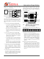
The pads used to load the defaults values of the
registers and the boot mode are:
• BT1, BT0: These two inputs are used to select the
boot mode, as depicted from Table 8.1
BT1
BT0
Boot mode
0
0
2-wire boot mode.
0
1
SPI boot mode.
1
0
SCI boot mode.
1
1
External Memory mode.
Table 8.1: Boot modes supported
• AD[15:8]: The addresses port is sampled in a high
to low transition of the reset signal to configure the
default values of the Serial Communication Block
Registers. The direction of this port is set as input
only if the reset signal is active; otherwise, the port
has output direction.
Stop Command
2-wire Register
Interpretation
x1xx xx10
Stop condition executing.
x1xx xx00
Stop command executed.
8. On-Reset Configuration
The FIPSOC chip has been designed to auto-boot after
reset. In order to bring more flexibility to the boot
process, different boot modes and configurations are
supported.
The information needed in the boot sequence is
obtained from the external system through the
input/output cells. The values set in some of the pads
are captured in the reset condition and stored in the
Serial Communication Block Registers. The program
boot later uses these values and configures the rest of
the chip.
Registers Configuration
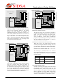
Tables 8.2, 8.3 and 8.4 list the correspondence between
the pads of the chip and the bits on the Serial
Communication Block registers.
SBCR
Value on reset
SCEN
not (BT1)
SCSL
not (BT0)
BMST
AD[15]
SCIE
0
GOE
0
ODS
AD[10]
IREN
not (BT1 and BT0)
BAUD
AD[8]
Table 8.2: SBCR register
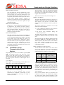
The boot modes supported are:
• 2-wire boot sequence: the Serial Communication
Block is configured as a 2-wire device. Both
address device and master/slave configuration can
be on-reset set
• SPI boot sequence: the Serial Comm. Block is
configured as an SPI device. Master/Slave
configuration can be on-reset set.
Chapter 8. Serial Communication Interface
17