1
SIDSA
Semiconductor Design Solutions
Serial Communication Interface
1. Overview
The Field Programmable System On Chip (FIPSOC)
constitutes a new concept in system integration. It
provides the user with the possibility of integrating a
microprocessor core along with programmable digital
and analog cells within the same integrated circuit.
This chip can be considered as a large granularity
FPGA with a FPAA (Field Programmable Analog
Array) and a built-in microprocessor core that does not
only act as a general purpose processing element, but
also configures the programmable cells and their
interconnections. Therefore, there is a strong
interaction between hardware and software as long as
signal values and configuration data within the
programmable
cells
are
accessible
from
microprocessor programs.
This chapter describes the Serial Communication
Block integrated on the FIPSOC system. It supports
two serial communication interfaces: a 2-wire protocol
and an SPI interface.
The 2-wire interface supports multi-devices serial data
communication using two lines. The 2-wire subblock
can be configured as either a master device or a slave
device. The block is identify by an address which can
be set via software.
The SPI interface is a synchronous interface which
allows several devices to be interconnected. Two wires
are required for data to obtain full duplex transfer
communication. A third line is used for clocking
purposes. The SPI subsystem supports different
communication rates and can be configured to be both
master or slave.
The Serial Communication Block would be
programmed by the software. However, it also supports
on-reset configuration (hardware configuration) in
order to provide more flexibility to the FIPSOC boot
procedure.
2. 2-Wire Serial Interface
This bus interface supports serial data transmission
using two lines between the devices connected to it.
The two wires are used to one for data (serial data –
SDA) and one for the clock signal (serial clock –SCL).
Multiple devices can be connected to the bus and can
operate as either a transmitter or receiver.
The transfer on the bus is initiated and controlled by a
master device that generates the clock signal; the other
devices, which send or receive data, are known as
slaves. Each device hanging in the bus is recognized by
an address. Any master-device must first identify the
desired slave by sending its address through the 2-wire
bus and configure it as either a transmitter or receiver
(read or write operations, respectively).
The 2-wire interface is multi-master. That is, more than
one device are capable of controlling the serial clock of
the bus.
2.1.
Bit Transfer
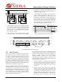
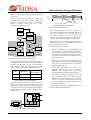
The transmission is controlled by the serial clock
(SCL). The SCL line is used to control each data bit
transferred. The data on the SDA line must be stable
during the high level of the SCL line. Level of the SDA
line can only change while the clock pulse on SCL is
low. Data changed during SCL high periods will
indicate a start or stop command (see figure 2.1).
bus free
bus busy
bus free
SCK
SDA
start condition
data valid
change of data
allowed
stop condition
Fig. 2.1: Bit transfer on the 2-wire interface
• Bus free: Both SDA and SCL are bi-directional
lines, connected to a positive supply via a pull-up
resistor (see figure 2.2). When the bus is free, no
transfer between any devices is in progress and
both lines stay high. All SDA and SCL outputs of
any devices connected to the bus must be opendrain (or open-collector) driven.
Note: 2-wire serial interface is not available in
device 8x12 of the FIPSOC family.
Chapter 8. Serial Communication Interface
2