1
MITSUBISHI ELECTRIC
MELSEC System Q
Programmable Logic Controllers
Users's Manual
QJ71PB92V
Profibus/DP Master
Art. no.: 166558
01 05 2007
SH (NA)-080572
Version C
MITSUBISHI ELECTRIC
INDUSTRIAL AUTOMATION
SAFETY PRECAUTIONS
(Read these precautions before using.)
Before using this product, please read this manual and the relevant manuals introduced in this manual
carefully and pay full attention to safety to handle the product correctly.
The instructions given in this manual are concerned with this product. For the safety instructions of the
programmable controller system, please read the user's manual of the CPU module used.
In this manual, the safety instructions are ranked as "DANGER" and "CAUTION".
DANGER
Indicates that incorrect handling may cause hazardous conditions,
resulting in death or severe injury.
CAUTION
Indicates that incorrect handling may cause hazardous conditions,
resulting in medium or slight personal injury or physical damage.
Note that the
CAUTION level may lead to a serious consequence according to the circumstances.
Always follow the instructions of both levels because they are important to personal safety.
Please save this manual to make it accessible when required and always forward it to the end user.
[DESIGN PRECAUTIONS]
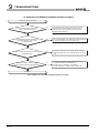
DANGER
When a communication error occurs on PROFIBUS-DP, the status of the faulty station is as shown
below.
Create an interlock circuit in the sequence program using the communication status information to
ensure the system operates safely (Input X1, buffer memory 5A20H to 5B19H (23072 to 23321)).
An erroneous output or malfunction may cause accidents.
(1) The QJ71PB92V holds the input data before the communication failure.
(2) When the QJ71PB92V has gone down, the output status of each DP-Slave is dependent on the
QJ71PB92V parameter setting on GX Configurator-DP.
(3) When a DP-Slave has gone down, the output status of the other DP-Slaves is dependent on the
QJ71PB92V parameter setting on GX Configurator-DP.
Do not output the "use prohibited" signal as the output signal to an intelligent function module from
the programmable controller CPU.
Wiring data into the "system area" or outputting a signal for "use prohibited" may cause system
malfunction in the programmable controller.
A-1
[DESIGN PRECAUTIONS]
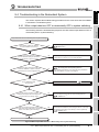
DANGER
When a stop error has occurred to the CPU module, the communication status varies depending on
the error time output mode setting of GX Developer as shown below.
Set the communication status for when a stop error has occurred to the CPU module according to the
system specifications.
Note that, if the QJ71PB92V is mounted to a redundant system, it operates as described in (1) below
regardless of the setting.
(1) When "Error time output mode" is set to "Hold".
(a) Since the communication with the DP-Slave is continued, values at the time of the CPU
module stop error occurrence are held as the output data sent to the DP-Slave from the
QJ71PB92V.
(b) Input data received from DP-Slaves are updated into the buffer memory of the QJ71PB92V.
(2) When "Error time output mode" is set to "Clear"
(a) Communications with DP-Slaves are interrupted, and output data are not sent.
(b) Input data received from DP-Slaves are held in the buffer memory of the QJ71PB92V.
When the QJ71PB92V is mounted in a redundant system, set the watchdog timer for DP-Slaves so
that the calculation formula shown in Section 4.8 (5) is satisfied.
If the formula is not satisfied, a watchdog timer error occurs in DP-Slaves during system switching.
CAUTION
Do not install PROFIBUS cables together with the main circuit or power lines or bring them close to
each other.
Keep a distance of 100mm (3.9inch) or more between them.
Failure to do so may cause malfunctions due to noise.
A-2
[INSTALLATION PRECAUTIONS]
CAUTION
Use the programmable controller under the environment specified in the user’s manual of the CPU
module to be used.
Otherwise, it may cause electric shocks, fires, malfunctions, product deterioration or damage.
While pressing the installation lever located at the bottom of the module, insert the module fixing
projection into the fixing hole in the base unit to mount the module.
Incorrect mounting may cause malfunctions, a failure or a drop of the module.
In an environment of frequent vibrations, secure the module with the screw.
Tighten the screw within the specified torque range.
If the screw is too loose, it may cause a drop of the module, a short circuit or malfunctions.
Overtightening may damage the screw and/or the module, resulting in a drop of the module, a short
circuit or malfunctions.
Be sure to shut off all phases of the external power supply used by the system before mounting or
removing the module.
Failure to do so may damage the module.
A-3
[INSTALLATION PRECAUTIONS]
CAUTION
Do not directly touch the conductive part or electronic components of the module.
Doing so may cause malfunctions or a failure of the module.
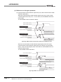
[WIRING PRECAUTIONS]
DANGER
Be sure to shut off all phases of the external power supply used by the system before wiring
PROFIBUS cables.
Failure to do so may result in failure or malfunctions of the module.
CAUTION
Carefully prevent foreign matter such as dust or wire chips from entering the module.
Failure to do so may cause a fire, failure or malfunctions.
Be sure to place the PROFIBUS cables in a duct or clamp them.
If not, dangling cables may be shifted or inadvertently pulled, resulting in damages to the module or
cables or malfunctions due to poor cable contact.
When disconnecting the PROFIBUS cable, do not pull it by holding the cable part.
Be sure to hold its connector which is plugged into the module.
Pulling the cable with it connected to the module may damage the module and/or cable, or cause
malfunctions due to poor contact of the cable.
A protective film is attached onto the module top to prevent foreign matter such as wire chips from
entering the module when wiring.
Do not remove the film during wiring.
Remove it for heat dissipation before system operation.
A-4
[STARTING AND MAINTENANCE PRECAUTIONS]
DANGER
Before cleaning, be sure to shut off all phases of the external power supply used by the system.
Failure to do so may cause electrical shocks.
CAUTION
Do not disassemble or modify the module.
Doing so may cause failure, malfunctions, personal injuries and/or a fire.
When using a wireless communication device such as a cellular phone or a PHS, keep it at least
25cm (9.85 inch) away from the entire programmable controller system in all directions.
Failure to do so may cause a malfunction.
Be sure to shut off all phases of the external power supply before mounting or removing the module.
Failure to do so may result in failure or malfunctions of the module.
Module installation to or removal from the base unit is limited to 50 times after the first use of the
product. (IEC 61131-2 compliant)
Exceeding 50 times may cause malfunctions.
Before handling modules, touch a grounded metal object to discharge the static electricity from the
human body.
Not doing so may cause failure or malfunctions of the module.
[DISPOSAL PRECAUTIONS]
CAUTION
When disposing of this product, treat is as an industrial waste.
A-5
REVISIONS
* The manual number is given on the bottom left of the back cover.
Print Date
* Manual Number
Aug., 2005
SH (NA)-080572ENG-A
Jun., 2006
SH (NA)-080572ENG-B
Revision
First edition
Modifications
SAFETY PRECAUTIONS, GLOSSARY, Section 1.1, 2.1, 2.2.1, 2.4, 3.1 to
3.5, CHAPTER 4, Section 4.1.1, 4.1.3, 4.2.1 to 4.2.3, 4.5, 4.6, 5.3, 5.4, 6.1 to
6.3, 6.5, 6.6.4, CHAPTER 7 to Section 7.1.3, 9.4, Appendix 2
Additions
2.3 , 3.5.3, 4.7, 4.8, 5.2.2, 6.7, 7.7, 7.9, 8.1, 9.3, 9.4.1 to 9.4.6, Appendix 1
Section number changes
Section 5.2
5.2.1, Section 7.7
7.8, Section 8.1 to 8.2
Section 8.3, Appendix 1 to Appendix 2
May, 2007
SH (NA)-080572ENG-C
Section 8.2 to
Appendix 2 to Appendix 3
• Rewritten to include the QJ71PB92D-compatible function.
• Modified for descriptions of GX Configurator-DP Version 7.02C.
Change of a term
"PLC" was changed to "programmable controller".
Modifications
SAFETY PRECAUTIONS, ABOUT THE GENERIC TERMS AND
ABBREVIATIONS, ABOUT MANUALS, GLOSSARY, CHAPTER 1, Section
1.1, 2.1, 2.4, 3.5.1, 4.5, 4.6, 5.3, 6.1, 6.3 to 6.7, CHAPTER 7, Section 8.1 to
8.3, CHAPTER 9 to Section 9.1, 9.3, 9.5.1 to 9.5.6, Appendix 1 to 2.3
Additions
Section 4.9, 9.2
Section number changes
Section 9.2 to 9.5
9.3 to 9.6
Japanese Manual Version SH-080571-C
This manual confers no industrial property rights or any rights of any other kind, nor does it confer any patent licenses.
Mitsubishi Electric Corporation cannot be held responsible for any problems involving industrial property rights which may
occur as a result of using the contents noted in this manual.
2005 MITSUBISHI ELECTRIC CORPORATION
A-6
INTRODUCTION
Thank you for purchasing the Mitsubishi programmable controller, MELSEC-Q series.
Please read this manual carefully before use to develop familiarity with the functions and performance, and
use it correctly.
CONTENTS
SAFETY PRECAUTIONS•••••••••••••••••••••••••••••••••••••••••••••••••••••••••••••••••••••••••••••••••••••••••••••••••••••• A - 1
REVISIONS••••••••••••••••••••••••••••••••••••••••••••••••••••••••••••••••••••••••••••••••••••••••••••••••••••••••••••••••••••••• A - 6
INTRODUCTION •••••••••••••••••••••••••••••••••••••••••••••••••••••••••••••••••••••••••••••••••••••••••••••••••••••••••••••••• A - 7
CONTENTS••••••••••••••••••••••••••••••••••••••••••••••••••••••••••••••••••••••••••••••••••••••••••••••••••••••••••••••••••••••• A - 7
ABOUT MANUALS ••••••••••••••••••••••••••••••••••••••••••••••••••••••••••••••••••••••••••••••••••••••••••••••••••••••••••••• A - 11
COMFORMANCE TO THE EMC AND LOW VOLTAGE DIRECTIVES•••••••••••••••••••••••••••••••••••••••••••••• A - 11
ABOUT THE GENERIC TERMS AND ABBREVIATIONS•••••••••••••••••••••••••••••••••••••••••••••••••••••••••••••• A - 12
GLOSSARY•••••••••••••••••••••••••••••••••••••••••••••••••••••••••••••••••••••••••••••••••••••••••••••••••••••••••••••••••••••• A - 13
PACKING LIST•••••••••••••••••••••••••••••••••••••••••••••••••••••••••••••••••••••••••••••••••••••••••••••••••••••••••••••••••• A - 14
CHAPTER1 OVERVIEW
1.1
Features ••••••••••••••••••••••••••••••••••••••••••••••••••••••••••••••••••••••••••••••••••••••••••••••••••••••••••••••1 - 3
CHAPTER2 SYSTEM CONFIGURATION
2.1
Basic configuration of the PROFIBUS-DP network•••••••••••••••••••••••••••••••••••••••••••••••••••••2 - 5
PROFIBUS-DP network configuration examples •••••••••••••••••••••••••••••••••••••••••••••••••••••••2 - 6
Redundant System Configuration (Redundant CPUs Only) •••••••••••••••••••••••••••••••••••••••••••••••• 2 - 8
2.3.1
2.3.2
2.4
Precautions for use on MELSECNET/H remote I/O stations ••••••••••••••••••••••••••••••••••••••••• 2 - 4
PROFIBUS-DP Network Configuration •••••••••••••••••••••••••••••••••••••••••••••••••••••••••••••••••••••••••2 - 5
2.2.1
2.2.2
2.3
2 - 1 to 2 - 15
Applicable System •••••••••••••••••••••••••••••••••••••••••••••••••••••••••••••••••••••••••••••••••••••••••••••••••2 - 1
2.1.1
2.2
1 - 1 to 1 - 6
PROFIBUS-DP network configuration •••••••••••••••••••••••••••••••••••••••••••••••••••••••••••••••••••• 2 - 8
PROFIBUS-DP network configuration examples •••••••••••••••••••••••••••••••••••••••••••••••••••••••2 - 9
Checking the Function Version and Serial No.•••••••••••••••••••••••••••••••••••••••••••••••••••••••••••••• 2 - 14
CHAPTER3 SPECIFICATIONS
3 - 1 to 3 - 67
3.1
Performance Specifications••••••••••••••••••••••••••••••••••••••••••••••••••••••••••••••••••••••••••••••••••••••• 3 - 1
3.2
Function List•••••••••••••••••••••••••••••••••••••••••••••••••••••••••••••••••••••••••••••••••••••••••••••••••••••••••3 - 3
3.3
Input/Output Signals to/from Programmable Controller CPU ••••••••••••••••••••••••••••••••••••••••••••••3 - 4
3.3.1
3.3.2
3.4
List of I/O signals •••••••••••••••••••••••••••••••••••••••••••••••••••••••••••••••••••••••••••••••••••••••••••••• 3 - 4
Details of I/O signals••••••••••••••••••••••••••••••••••••••••••••••••••••••••••••••••••••••••••••••••••••••••••3 - 6
Buffer Memory ••••••••••••••••••••••••••••••••••••••••••••••••••••••••••••••••••••••••••••••••••••••••••••••••••••• 3 - 17
3.4.1
3.4.2
3.4.3
3.4.4
Buffer memory list ••••••••••••••••••••••••••••••••••••••••••••••••••••••••••••••••••••••••••••••••••••••••••• 3 - 17
Local station information area •••••••••••••••••••••••••••••••••••••••••••••••••••••••••••••••••••••••••••• 3 - 21
Operation mode change area••••••••••••••••••••••••••••••••••••••••••••••••••••••••••••••••••••••••••••• 3 - 23
I/O data exchange area •••••••••••••••••••••••••••••••••••••••••••••••••••••••••••••••••••••••••••••••••••• 3 - 24
A-7
3.4.5
3.4.6
3.4.7
3.4.8
3.4.9
3.4.10
3.4.11
3.4.12
3.4.13
3.4.14
3.5
Slave status area •••••••••••••••••••••••••••••••••••••••••••••••••••••••••••••••••••••••••••••••••••••••••••• 3 - 29
Diagnostic information area ••••••••••••••••••••••••••••••••••••••••••••••••••••••••••••••••••••••••••••••• 3 - 36
Extended diagnostic information read area •••••••••••••••••••••••••••••••••••••••••••••••••••••••••••• 3 - 42
Bus cycle time area ••••••••••••••••••••••••••••••••••••••••••••••••••••••••••••••••••••••••••••••••••••••••• 3 - 43
Global control area•••••••••••••••••••••••••••••••••••••••••••••••••••••••••••••••••••••••••••••••••••••••••• 3 - 44
Acyclic communication area •••••••••••••••••••••••••••••••••••••••••••••••••••••••••••••••••••••••••••••• 3 - 46
Alarm area •••••••••••••••••••••••••••••••••••••••••••••••••••••••••••••••••••••••••••••••••••••••••••••••••••• 3 - 50
Time control area•••••••••••••••••••••••••••••••••••••••••••••••••••••••••••••••••••••••••••••••••••••••••••• 3 - 50
Temporary slave reservation area ••••••••••••••••••••••••••••••••••••••••••••••••••••••••••••••••••••••• 3 - 51
Redundant system area•••••••••••••••••••••••••••••••••••••••••••••••••••••••••••••••••••••••••••••••••••• 3 - 53
Processing Time •••••••••••••••••••••••••••••••••••••••••••••••••••••••••••••••••••••••••••••••••••••••••••••••••• 3 - 58
3.5.1
3.5.2
3.5.3
Bus cycle time ••••••••••••••••••••••••••••••••••••••••••••••••••••••••••••••••••••••••••••••••••••••••••••••• 3 - 58
Transmission delay time ••••••••••••••••••••••••••••••••••••••••••••••••••••••••••••••••••••••••••••••••••• 3 - 62
System switching time in redundant system ••••••••••••••••••••••••••••••••••••••••••••••••••••••••••• 3 - 64
CHAPTER4 FUNCTIONS
4.1
PROFIBUS-DPV0 Functions •••••••••••••••••••••••••••••••••••••••••••••••••••••••••••••••••••••••••••••••••••••4 - 2
4.1.1
4.1.2
4.1.3
4.2
I/O data exchange•••••••••••••••••••••••••••••••••••••••••••••••••••••••••••••••••••••••••••••••••••••••••••••4 - 2
Acquisition of diagnostic and/or extended diagnostic information •••••••••••••••••••••••••••••••••••4 - 4
Global control function •••••••••••••••••••••••••••••••••••••••••••••••••••••••••••••••••••••••••••••••••••••••4 - 7
PROFIBUS-DPV1 Functions ••••••••••••••••••••••••••••••••••••••••••••••••••••••••••••••••••••••••••••••••••• 4 - 11
4.2.1
4.2.2
4.2.3
4.3
4 - 1 to 4 - 45
Acyclic communication with DP-Slaves ••••••••••••••••••••••••••••••••••••••••••••••••••••••••••••••••• 4 - 11
Alarm acquisition •••••••••••••••••••••••••••••••••••••••••••••••••••••••••••••••••••••••••••••••••••••••••••• 4 - 14
FDT/DTM technology••••••••••••••••••••••••••••••••••••••••••••••••••••••••••••••••••••••••••••••••••••••• 4 - 16
PROFIBUS-DPV2 Functions ••••••••••••••••••••••••••••••••••••••••••••••••••••••••••••••••••••••••••••••••••• 4 - 17
4.3.1
Time control over DP-Slaves•••••••••••••••••••••••••••••••••••••••••••••••••••••••••••••••••••••••••••••• 4 - 17
4.4
Data Swap Function •••••••••••••••••••••••••••••••••••••••••••••••••••••••••••••••••••••••••••••••••••••••••••••• 4 - 19
4.5
Data Consistency Function ••••••••••••••••••••••••••••••••••••••••••••••••••••••••••••••••••••••••••••••••••••• 4 - 21
4.6
Output Status Setting for the Case of a CPU Stop Error •••••••••••••••••••••••••••••••••••••••••••••••••• 4 - 24
4.7
Temporary slave reservation function••••••••••••••••••••••••••••••••••••••••••••••••••••••••••••••••••••••••• 4 - 27
4.8
Redundant system support function••••••••••••••••••••••••••••••••••••••••••••••••••••••••••••••••••••••••••• 4 - 29
4.9
QJ71PB92D-Compatible Function••••••••••••••••••••••••••••••••••••••••••••••••••••••••••••••••••••••••••••• 4 - 40
CHAPTER5 PROCEDURES AND SETTINGS BEFORE SYSTEM OPERATION5 - 1 to 5 - 11
5.1
Implementation and Installation ••••••••••••••••••••••••••••••••••••••••••••••••••••••••••••••••••••••••••••••••••5 - 1
5.1.1
5.2
Handling precautions •••••••••••••••••••••••••••••••••••••••••••••••••••••••••••••••••••••••••••••••••••••••••5 - 1
Procedures and Settings before System Operation••••••••••••••••••••••••••••••••••••••••••••••••••••••••••5 - 2
5.2.1
5.2.2
In the case of the single CPU system •••••••••••••••••••••••••••••••••••••••••••••••••••••••••••••••••••••5 - 2
In the case of the redundant system ••••••••••••••••••••••••••••••••••••••••••••••••••••••••••••••••••••••5 - 3
5.3
Part Names and Settings ••••••••••••••••••••••••••••••••••••••••••••••••••••••••••••••••••••••••••••••••••••••••••5 - 5
5.4
Self-diagnostics •••••••••••••••••••••••••••••••••••••••••••••••••••••••••••••••••••••••••••••••••••••••••••••••••••••5 - 7
5.5
Wiring •••••••••••••••••••••••••••••••••••••••••••••••••••••••••••••••••••••••••••••••••••••••••••••••••••••••••••••••••5 - 9
5.5.1
5.5.2
A-8
PROFIBUS cable wiring •••••••••••••••••••••••••••••••••••••••••••••••••••••••••••••••••••••••••••••••••••••5 - 9
Wiring precautions •••••••••••••••••••••••••••••••••••••••••••••••••••••••••••••••••••••••••••••••••••••••••• 5 - 11
CHAPTER6 PARAMETER SETTING
6 - 1 to 6 - 25
6.1
Parameter Setting Procedure•••••••••••••••••••••••••••••••••••••••••••••••••••••••••••••••••••••••••••••••••••••6 - 1
6.2
Operation Mode Setting •••••••••••••••••••••••••••••••••••••••••••••••••••••••••••••••••••••••••••••••••••••••••••6 - 4
6.3
Master Parameters •••••••••••••••••••••••••••••••••••••••••••••••••••••••••••••••••••••••••••••••••••••••••••••••••6 - 7
6.4
Bus Parameters ••••••••••••••••••••••••••••••••••••••••••••••••••••••••••••••••••••••••••••••••••••••••••••••••••• 6 - 10
6.5
Slave Parameters ••••••••••••••••••••••••••••••••••••••••••••••••••••••••••••••••••••••••••••••••••••••••••••••••• 6 - 12
6.6
Automatic Refresh Parameters •••••••••••••••••••••••••••••••••••••••••••••••••••••••••••••••••••••••••••••••• 6 - 16
6.6.1
6.6.2
6.6.3
6.6.4
6.7
Automatic refresh parameter setup procedure •••••••••••••••••••••••••••••••••••••••••••••••••••••••• 6 - 16
Automatic Refresh Settings ••••••••••••••••••••••••••••••••••••••••••••••••••••••••••••••••••••••••••••••• 6 - 17
Writing Automatic Refresh Parameters ••••••••••••••••••••••••••••••••••••••••••••••••••••••••••••••••• 6 - 21
Number of set automatic refresh parameters •••••••••••••••••••••••••••••••••••••••••••••••••••••••••• 6 - 22
Parameter Setting by GX Developer •••••••••••••••••••••••••••••••••••••••••••••••••••••••••••••••••••••••••• 6 - 24
CHAPTER7 PROGRAMMING
7.1
7 - 1 to 7 - 85
I/O Data Exchange Program Examples ••••••••••••••••••••••••••••••••••••••••••••••••••••••••••••••••••••••••7 - 2
7.1.1
7.1.2
7.1.3
Program examples using automatic refresh ••••••••••••••••••••••••••••••••••••••••••••••••••••••••••••• 7 - 6
Program example using dedicated instructions •••••••••••••••••••••••••••••••••••••••••••••••••••••••••7 - 9
Program example using the MOV instruction •••••••••••••••••••••••••••••••••••••••••••••••••••••••••• 7 - 11
7.2
Program Example for Acquisition of Extended Diagnostic Error Information•••••••••••••••••••••••••• 7 - 12
7.3
Program Example for Global Control Function•••••••••••••••••••••••••••••••••••••••••••••••••••••••••••••• 7 - 13
7.4
Program Example for Acyclic Communication with DP-Slaves •••••••••••••••••••••••••••••••••••••••••• 7 - 14
7.4.1
7.4.2
7.4.3
7.4.4
7.4.5
7.5
Program Example for Alarm Acquisition•••••••••••••••••••••••••••••••••••••••••••••••••••••••••••••••••••••• 7 - 30
7.5.1
7.5.2
7.5.3
7.5.4
7.6
READ services (Class1_SERVICE, Class2_SERVICE)••••••••••••••••••••••••••••••••••••••••••••• 7 - 16
WRITE services (Class1_SERVICE, Class2_SERVICE) ••••••••••••••••••••••••••••••••••••••••••• 7 - 19
INITIATE service (Class2_SERVICE)••••••••••••••••••••••••••••••••••••••••••••••••••••••••••••••••••• 7 - 22
ABORT service (Class2_SERVICE)••••••••••••••••••••••••••••••••••••••••••••••••••••••••••••••••••••• 7 - 26
Program example ••••••••••••••••••••••••••••••••••••••••••••••••••••••••••••••••••••••••••••••••••••••••••• 7 - 28
Alarm read request (without ACK) ••••••••••••••••••••••••••••••••••••••••••••••••••••••••••••••••••••••• 7 - 31
Alarm ACK request ••••••••••••••••••••••••••••••••••••••••••••••••••••••••••••••••••••••••••••••••••••••••• 7 - 35
Alarm read request (with ACK) ••••••••••••••••••••••••••••••••••••••••••••••••••••••••••••••••••••••••••• 7 - 40
Program example ••••••••••••••••••••••••••••••••••••••••••••••••••••••••••••••••••••••••••••••••••••••••••• 7 - 46
Program Example for Time Control over DP-Slaves••••••••••••••••••••••••••••••••••••••••••••••••••••••• 7 - 48
7.6.1
7.6.2
7.6.3
7.6.4
Time data read request •••••••••••••••••••••••••••••••••••••••••••••••••••••••••••••••••••••••••••••••••••• 7 - 49
Time data write request (UTC format)••••••••••••••••••••••••••••••••••••••••••••••••••••••••••••••••••• 7 - 51
Time data write request •••••••••••••••••••••••••••••••••••••••••••••••••••••••••••••••••••••••••••••••••••• 7 - 53
Program example ••••••••••••••••••••••••••••••••••••••••••••••••••••••••••••••••••••••••••••••••••••••••••• 7 - 55
7.7
Program Example for Temporary Slave Reservation •••••••••••••••••••••••••••••••••••••••••••••••••••••• 7 - 57
7.8
Program Example When Mounting the QJ71PB92V on a MELSECNET/H Remote I/O Network 7 - 58
7.8.1
7.8.2
7.9
Program example for the I/O data exchange function (When mounted on a remote I/O station) 7 58
Other precautions ••••••••••••••••••••••••••••••••••••••••••••••••••••••••••••••••••••••••••••••••••••••••••• 7 - 65
Program Examples for Use in the Redundant System •••••••••••••••••••••••••••••••••••••••••••••••••••• 7 - 66
7.9.1
7.9.2
I/O Data Exchange Program Examples••••••••••••••••••••••••••••••••••••••••••••••••••••••••••••••••• 7 - 70
Program example for acquisition of extended diagnostic error information•••••••••••••••••••••• 7 - 80
A-9
7.9.3
7.9.4
7.9.5
7.9.6
7.9.7
Program example for global control function••••••••••••••••••••••••••••••••••••••••••••••••••••••••••• 7 - 81
Program example for acyclic communication with DP-Slaves•••••••••••••••••••••••••••••••••••••• 7 - 82
Program example for alarm acquisition ••••••••••••••••••••••••••••••••••••••••••••••••••••••••••••••••• 7 - 83
Program example for time control over DP-Slaves ••••••••••••••••••••••••••••••••••••••••••••••••••• 7 - 83
Program example for temporary slave reservation ••••••••••••••••••••••••••••••••••••••••••••••••••• 7 - 85
CHAPTER8 DEDICATED INSTRUCTIONS
8 - 1 to 8 - 7
8.1
Precautions for Dedicated Instructions •••••••••••••••••••••••••••••••••••••••••••••••••••••••••••••••••••••••••8 - 2
8.2
G. BBLKRD ••••••••••••••••••••••••••••••••••••••••••••••••••••••••••••••••••••••••••••••••••••••••••••••••••••••••••8 - 4
8.3
G. BBLKWR••••••••••••••••••••••••••••••••••••••••••••••••••••••••••••••••••••••••••••••••••••••••••••••••••••••••••8 - 6
CHAPTER9 TROUBLESHOOTING
9 - 1 to 9 - 28
9.1
Error Check Using the LEDs and Corrective Actions ••••••••••••••••••••••••••••••••••••••••••••••••••••••••9 - 2
9.2
When Parameters cannot be Written from GX Configurator-DP ••••••••••••••••••••••••••••••••••••••••••9 - 4
9.3
When Communication with DP-Slaves Is Not Possible •••••••••••••••••••••••••••••••••••••••••••••••••••••9 - 6
9.4
Troubleshooting in the Redundant System ••••••••••••••••••••••••••••••••••••••••••••••••••••••••••••••••••••9 - 8
9.4.1
9.4.2
9.4.3
9.5
Error Codes •••••••••••••••••••••••••••••••••••••••••••••••••••••••••••••••••••••••••••••••••••••••••••••••••••••••• 9 - 12
9.5.1
9.5.2
9.5.3
9.5.4
9.5.5
9.5.6
9.6
When output data turn OFF or momentarily OFF in system switching••••••••••••••••••••••••••••••9 - 8
When the FAULT LED of the QJ71PB92V in the new control system is ON ••••••••••••••••••••••9 - 9
Maintenance of the QJ71PB92V in the standby system••••••••••••••••••••••••••••••••••••••••••••• 9 - 10
Error codes E200H to E2FFH (Error codes generated when reading extended diagnostic
information)9 - 13
Error codes E300H to E3FFH (Error codes generated when switching operation mode)••••• 9 - 14
Error codes E400H to E4FFH (Error codes generated during acyclic communication) ••••••• 9 - 15
Error codes E500H to E5FFH (Error codes generated when reading alarms) •••••••••••••••••• 9 - 20
Error codes E600H to E6FFH (Error codes generated when executing time control) ••••••••• 9 - 23
Error codes F100H to F1FFH (Local diagnostic information of the QJ71PB92V) •••••••••••••• 9 - 24
How to Return the QJ71PB92V to Its Factory-set Conditions•••••••••••••••••••••••••••••••••••••••••••• 9 - 27
APPENDICES
App - 1 to App - 21
Appendix 1
Functional Upgrade of the QJ71PB92V ••••••••••••••••••••••••••••••••••••••••••••••••••••••••••• App - 1
Appendix 2
Differences between the QJ71PB92V and Former Models •••••••••••••••••••••••••••••••••••• App - 1
Appendix 2.1 Specification comparisons••••••••••••••••••••••••••••••••••••••••••••••••••••••••••••••••••••••• App - 2
Appendix 2.2 Precautions for replacing the system•••••••••••••••••••••••••••••••••••••••••••••••••••••••••• App - 4
Appendix 2.3 Precautions for replacing programs ••••••••••••••••••••••••••••••••••••••••••••••••••••••••••• App - 6
Appendix 3 External Dimensions •••••••••••••••••••••••••••••••••••••••••••••••••••••••••••••••••••••••••••••••••App - 20
INDEX
A - 10
Index- 1 to Index- 2
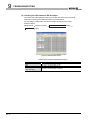
ABOUT MANUALS
The following manuals are related to this product.
Please purchase them if necessary.
Related Manuals
Manual Number
Manual Name
(Model Code)
GX Configurator-DP Version 7 Operating Manual
Explains the overview, installation method, screen operations, etc. of GX Configurator-DP Version 7.
(Sold separately)
GX Configurator-DP Operating Manual (CommDTM)
Explains the overview, installation and operating methods, etc, of MELSOFT PROFIBUS
CommDTM.
(Sold separately)
SH-080579ENG
(13JU54)
SH-080582ENG
(13JU55)
PROFIBUS-DP Interface Module User's Manual *1
Explains the overview of the QJ71PB92D-compatible function, system configurations, specifcations,
functions, procedures before system operation, programming, and dedicated instructions.
SH-080127
(13JR22)
(Sold separately)
*1
Refer to it when using the QJ71PB92D-compatible function.
COMFORMANCE TO THE EMC AND LOW VOLTAGE DIRECTIVES
When incorporating the Mitsubishi programmable controller into other
machinery or equipment and keeping compliance with the EMC and low
voltage directives, refer to Chapter 3 "EMC Directive and Low Voltage
Instruction" of the User’s Manual (hardware) supplied with your CPU
module or base unit.
The CE logo is printed on the rating plate of the programmable controller,
indicating compliance with the directives.
Note that no additional measures are necessary for this product to make
compliance with the directives.
A - 11
ABOUT THE GENERIC TERMS AND ABBREVIATIONS
Unless otherwise specified, this manual uses the following generic terms
and abbreviations to describe the Type QJ71PB92V PROFIBUS-DP
Master Module.
General term/Abbreviation
QJ71PB92V
PROFIBUS-DP
MELSECNET/H
QCPU
CPU module
Description
Abbreviation for the QJ71PB92V PROFIBUS-DP Master module.
Abbreviation of PROFIBUS-DP network
Abbreviation of MELSECNET/H network system
Generic term for the Q00JCPU, Q00CPU, Q01CPU, Q02CPU, Q02HCPU, Q06HCPU,
Q12HCPU, Q25HCPU, Q12PHCPU, Q25PHCPU, Q12PRHCPU, Q25PRHCPU,
Redundant CPU
Q03UDCPU, Q04UDHCPU and Q06UDHCPU
Generic term for the Q12PRHCPU and Q25PRHCPU
Generic product name for SWnD5C-GPPW-E, SWnD5C-GPPW-EA, SWnD5C-GPPW-EV,
GX Developer
and SWnD5C-GPPW-EVA. ("n" means version 4 or later.)
GX Configurator-DP
BBLKRD
BBLKWR
A - 12
"-A" and "-V" mean "volume license product" and "version-upgrade product" respectively.
Configuration tool for QJ71PB92V
Generic term of the product model SWnD5C-PROFID-E ("n" means version 7 or later.)
Abbreviation for G. BBLKRD
Abbreviation for G. BBLKWR
GLOSSARY
This part explains the glossary used in this manual.
Term
Description
A basic version of PROFIBUS-DP.
The following functions are executable:
PROFIBUS-DPV0
• I/O data exchange
• Diagnostic information notification
etc.
A PROFIBUS-DP version for which the following functions have been added to the basic
functionality of PROFIBUS-DPV0
PROFIBUS-DPV1
• Acyclic communication
• Alarm function
etc.
A PROFIBUS-DP version for which the following functions have been added to the
PROFIBUS-DPV2
Class 1
DP-Master
Class 2
DP-Slave
Repeater
Bus terminator
Configuration tool
GSD file
FDL address
Bus parameter
Master parameter
PROFIBUS-DPV1 functionality
• Time stamping
etc.
A device exchanging I/O data with a DP-Slaves. (QJ71PB92V, QJ71PB92D, etc)
A device that communicates with DP-Slaves and checks their FDL address settings and/or
operation states
The DP-Master (Class 2) is used as a DP-Master for supervising the network, which can start,
maintain, and diagnose the system.
A device that exchanges I/O data with a DP-Master (Class 1). (QJ71PB93D, ST1H-PB, etc)
A device used to connect different segments of PROFIBUS-DP
A terminating resistor that is connected to either end of each segment on PROFIBUS-DP
Software used to set bus parameters, slave parameters, etc. and to write them to a DP-Master
(GX Configurator-DP, etc.)
An electronic file that contains parameters of a DP-Slave
The GSD file is used to set up the slave parameters on GX Configurator-DP.
The numbers assigned to a DP-Master and DP-Slaves
The FDL address is set within the range from 0 to 125.
The parameter used for the communication setting of PROFIBUS-DP
The bus parameter is set up on the GX Configurator-DP.
The parameter used for the settings (FDL address, transmission speed, etc.) of the
QJ71PB92V
The master parameter is set up on the GX Configurator-DP.
The parameter for a DP-Slave, which is set on the DP-Master.
Slave parameter
The slave parameter is set up on the GX Configurator-DP.
The setting items are described on the GSD File.
I/O CONFIGURATION
DATA
I/O data exchange
Global control
Diagnostic information
Information on I/O configuration of a DP-Slave
This function allows I/O data exchange between a DP-Master (Class 1) and DP-Slaves.
This function enables synchronization command transmission for I/O data from a DP-Master
(Class 1) to DP-Slaves.
Diagnostic information of PROFIBUS-DP, which is detected by a DP-Master or notified by a
Extended diagnostic error
DP-Slave
Diagnostic information specific to each DP-Slave
information
Each of DP-Slaves notifies of it to the DP-Master when an error is detected.
(To the next page)
A - 13
Term
Description
PROFIBUS-DP processing time for the DP-Master to perform cyclic communication with each
Bus cycle time
DP-Slave
A tool by which the following operations are performed to DP-Slaves on the PROFIBUS-DP via
a DP-Master
FDT
• Writing or reading parameters of DP-Slaves
(Field Device Tool)
• Monitoring DP-Slave status
etc.
A file in which communication settings and DP-Slave parameters are defined when FDT is used
DTM
(Device Type Manager)
The DTM consists of CommDTM and DeviceDTM.
An abbreviation of Communication DTM
CommDTM
CommDTM is a file used to define the communication settings needed for transmission via a
DeviceDTM
DP-Master.
Device DTM is a file in which parameters to be set for a DP-Slave are defined.
A specific number for each module that is connected to PROFIBUS-DP
Ident No.
Ident No. is described in a GSD file of each module.
The UTC is based on the UTC, which stands for Coordinated Universal Time.
UTC
In order to adjust the time gap with the GMT (Greenwich Mean Time), the "leap second" has
Time master
System A
System B
Control system
Standby system
been added.
A master station that can send a request for time control.(QJ71PB92V, etc.)
The system to which the system-A connector of the tracking cable is connected.
The system to which the system-B connector of the tracking cable is connected.
The system that is controlling the redundant system and performing network communication
The system for backup in the redundant system
The system changed from the standby system status to the control system status due to system
New control system
switching
The system changed from the control system status to the standby system status due to system
New standby system
QJ71PB92D-compatible
function
switching
The function used to replace the QJ71PB92D with the QJ71PB92V
The QJ71PB92V type PROFIBUS-DP master module has this function.
QJ71PB92D The QJ71PB92D type PROFIBUS-DP interface module
PACKING LIST
The following indicates the packing list of the QJ71PB92V.
Model
QJ71PB92V
A - 14
Product name
QJ71PB92V PROFIBUS-DP master module
Quantity
1
1
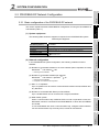
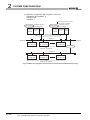
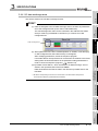
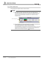
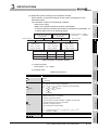
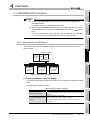
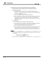
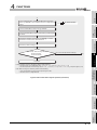
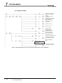
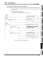
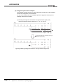
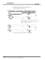
OVERVIEW
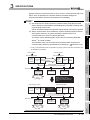
1
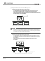
Single CPU system
DP-Master (Class 1)(QJ71PB92V)
2
SYSTEM
CONFIGURATION
This manual explains the specifications, functions, procedures before system operation,
and troubleshooting for the QJ71PB92V PROFIBUS-DP master module (hereinafter
referred to as "QJ71PB92V").
The QJ71PB92V is used for connecting MELSEC-Q Series programmable controllers to
PROFIBUS-DP.
The QJ71PB92V operates as a DP-Master (Class 1) on PROFIBUS-DP networks.
OVERVIEW
CHAPTER1 OVERVIEW
DP-Slave (QJ71PB93D)
DP-Slave ( MELSEC-ST system)
S T 1 PS D
S T1 H- P B
Bus terminator
RUN
ERR
SYS
SPECIFICATIONS
3
DP-Slave
S T 1 PD D
RUN
11
ERR
21
RUN
11
ERR
RUN
ERR
RUN
ERR
RUN
ERR
4
21
AUX
.
AUX
RELEASE
RESET
Bus terminator
PROCEDURES AND
SETTINGS BEFORE
SYSTEM OPERATION
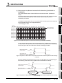
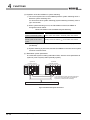
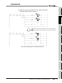
5
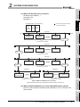
Standby system
6
PARAMETER SETTING
Tracking cable
Bus terminator
DP-Slave
(QJ71PB93D)
DP-Slave
(MELSEC-ST System)
ST1PSD
ST1H-PB
RUN
SYS
AUX .
DP-Slave
7
ST1PDD
ERR
RUN
11
ERR
21
RUN
11
ERR
RUN
ERR
RUN
ERR
RUN
ERR
21
AUX
RELEASE
RESET
PROFIBUS I/F
Bus terminator
Figure 1.1 PROFIBUS-DP Using QJ71PB92V
PROGRAMMING
Control system
Redundant CPU (Q25PRHCPU)
DP-Master (Class 1) (QJ71PB92V)
8
1-1
DEDICATED
INSTRUCTIONS
Redundant system
FUNCTIONS
PROFIBUS I/F
1
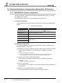
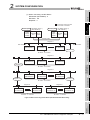
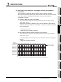
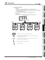
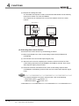
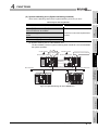
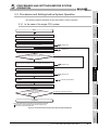
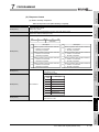
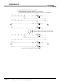
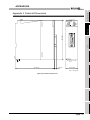
OVERVIEW
MELSECNET/H remote I/O network
Remote master station (QJ71LP21-25 )
MELSECNET/H
Remote I/O network
Remote I/O station ( QJ72LP25-25 )
DP-Master (Class 1)(QJ71PB92V)
DP-Slave (QJ71PB93D)
DP-Slave (MELSEC-ST System)
S T 1 PS D
S T1 H- P B
Bus terminator
RUN
SYS
AUX
.
ERR
DP-Slave
S T 1 PD D
RUN
11
ERR
21
RUN
11
ERR
RUN
ERR
RUN
ERR
RUN
ERR
21
AUX
RELEASE
RESET
PROFIBUS I/F
Bus terminator
Figure 1.1 PROFIBUS-DP Using QJ71PB92V (Continued)
Remark
The QJ71PB92V has a function for replacing the QJ71PB92D with the
QJ71PB92V. (QJ71PB92D-compatible function)
When the QJ71PB92D has failed, replace it with the QJ71PB92V using the
QJ71PB92D-compatible function.
Table1.1 Reference Manuals
Purpose
PROFIBUS-DP Master Module User's
PROFIBUS-DP Interface Module User's
Manual
Manual
Details
—
Outline
Details
Using the functions of the
QJ71PB92V
Replacing the QJ71PB92D with the
QJ71PB92V using the
QJ71PB92D-compatible function
1-2
OVERVIEW
1
OVERVIEW
1.1 Features
The following describes the features of the QJ71PB92V.
(1) DP-Master (Class 1) on PROFIBUS-DP
Up to 125 DP-Slaves*1 can be connected to a single QJ71PB92V, enabling
Section 4.1.1)
* 1 Up to 124 DP-Slaves when the QJ71PB92V is used in a redundant system.
(b) Diagnostic information can be easily acquired
Diagnostic or extended diagnostic information of an error occurred on a DP-Slave
during I/O data exchange can be easily acquired using the buffer memory and I/O
Section 4.1.2)
(c) Supporting the global control function
By sending services (SYNC, UNSYNC, FREEZE, UNFREEZE) to each DP-Slave
Table1.2 Descriptions of Services
Service Name
Description
This service is for synchronizing the output status of DP-Slaves.
SYNC
UNSYNC
In the SYNC mode, the output status of a DP-Slave is refreshed
each time it receives the SYNC service.
While no SYNC service is received, the output status is held.
This service is for ending the SYNC mode.
This service is for synchronizing the input status of DP-Slaves.
FREEZE
UNFREEZE
In the FREEZE mode, the input status of a DP-Slave is refreshed
each time it receives the FREEZE service.
While no FREEZE service is received, the input status is held.
This service is for ending the FREEZE service.
(d) Supporting PROFIBUS-DPV1 and PROFIBUS-DPV2
PROFIBUS-DPV1 and PROFIBUS-DPV2, which are extended versions of
PROFIBUS-DP, are supported
The QJ71PB92V supports the following:
• FDT/DTM technology (
Section 4.2.1)
Section 4.2.2)
Section 4.2.3)
2) PROFIBUS-DPV2
• Time control function on DP-Slaves (
Section 4.3.1)
1.1 Features
6
PROGRAMMING
• Alarm acquisition (
5
7
1) PROFIBUS-DPV1
• Acyclic communication with DP-Slaves (
FUNCTIONS
Section
PROCEDURES AND
SETTINGS BEFORE
SYSTEM OPERATION
in a group, synchronous control of DP-Slave I/O data is available.(
4.1.3)
4
PARAMETER SETTING
signals. (
3
SPECIFICATIONS
(a) Up to 125 DP-Slaves are connectable
exchange of I/O data up to 8192 bytes.(
2
SYSTEM
CONFIGURATION
The QJ71PB92V complies with IEC 61158, and operates as a DP-Master (Class 1) on
PROFIBUS-DP systems.
8
1-3
DEDICATED
INSTRUCTIONS
1
1
OVERVIEW
(2) I/O data consistency
Using the automatic refresh setting in GX Configurator-DP or dedicated instructions
(BBLKRD/BBLKWR) ensures data consistency when reading/writing I/O data from the
QJ71PB92V buffer memory. (
Section 4.5)
(3) Easy parameter setup
Use of GX Configurator-DP enables bus parameters, master parameters, slave
parameters, and various other parameters to be easily set up. (
CHAPTER 6)
(4) Swapping of I/O data
The upper and lower bytes can be reversed (swapped) in word units when I/O data is
sent or received.
This simplifies programming as you no longer need to create a program for swapping
the upper and lower bytes on the QJ71PB92V or DP-Slave. (
Section 4.4)
(5) Mountable on MELSECNET/H remote I/O station
The QJ71PB92V can be mounted on a MELSECNET/H remote I/O station.
This allows you to install the QJ71PB92V at a remote site away from the QCPU.
(
Section 7.8)
(6) Output status setting for the case of a CPU stop error (Stop/Continue of
I/O data exchange)
For the case of a CPU stop error on a QCPU or remote I/O station where the
QJ71PB92V is mounted, whether to stop or continue I/O data exchange with DPSlaves can be specified. (
Section 4.6)
(7) Changing DP-Slave setting to reserved station status temporarily
Without modifying the slave parameter in GX Configurator-DP, the station type of DPSlaves can be changed to "Reserved station" temporarily. (
Section 4.7)
Since there is no need to change slave parameters, changing a DP-Slave setting to a
reserved station is easy.
1-4
1.1 Features
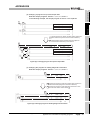
OVERVIEW
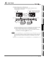
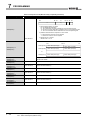
1
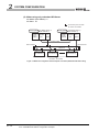
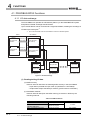
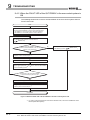
(a) Redundancy is available for the QJ71PB92V.
By mounting the QJ71PB92V together with a redundant CPU, a redundant
system can be constructed.
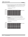
Even if the QJ71PB92V detects an error, the control and standby systems are
• When the QJ71PB92V detects a critical error
Standby system
Error in
QJ71PB92V
New standby system
Continues communication
New control system
SYSTEM
CONFIGURATION
Section 4.8)
(b) System switching is available when an error occurs in the QJ71PB92V or in
communication with a DP-Slave.
The systems can be switched when an error occurs in the QJ71PB92V or in
communication with a DP-Slave.
Control system
2
3
SPECIFICATIONS
switched each other continuing communications.(
OVERVIEW
(8) Redundant system can be constructed
4
System switching
Bus terminator
ST1H-PB
ST1PSD
RUN
ERR
SYS
RUN
11
AUX.
ERR
21
RUN
11
ERR
21
ST1PDD
RUN
ERR
RUN
ERR
RUN
ERR
AUX
5
RELEASE
RESET
PROCEDURES AND
SETTINGS BEFORE
SYSTEM OPERATION
PROFIBUS I/F
DP-Slave (QJ71PB93D)
DP-Slave (ST1H-PB)
Figure 1.2 When the QJ71PB92V detects a critical error
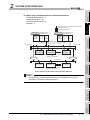
• When the QJ71PB92V detects a communication error of a DP-Slave
Standby system
New standby system
New control system
PARAMETER SETTING
6
Control system
Continues communication
System switching
7
Tracking cable
Bus terminator
PROGRAMMING
Bus terminator
FUNCTIONS
Tracking cable
Bus terminator
Communication
failure
8
Figure 1.3 When the QJ71PB92V detects a communication error of a DP-Slave
1.1 Features
1-5
DEDICATED
INSTRUCTIONS
1
1
OVERVIEW
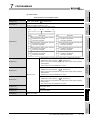
(9) QJ71PB92D can be easily replaced with QJ71PB92V.
The QJ71PB92V has a function for replacing the QJ71PB92D with the QJ71PB92V.
(
Section 4.9)
Since the existing network configuration and sequence programs for the QJ71PB92D
can be utilized, a faulty QJ71PB92D can be smoothly replaced with the QJ71PB92V.
QJ71PB92D
failed
Replaced
QJ71PB92V
(QJ71PB92D-compatible function)
Figure 1.4 QJ71PB92D-Compatible Function
1-6
1.1 Features
2
SYSTEM CONFIGURATION
1
OVERVIEW
CHAPTER2 SYSTEM CONFIGURATION
This chapter explains the system configuration of the QJ71PB92V.
2.1 Applicable System
(1) Mountable modules, No. of mountable modules, and mountable base
unit
(a) When mounting to CPU module
The following shows the mountable CPU modules, No. of mountable modules,
and mountable base unit of the QJ71PB92V module.
Power shortage may occur depending on the combination with other mounted
modules or the number of mounted modules.
When mounting modules, pay attention to the power supply capacity.
When the power shortage occurs, review the combination of modules to be
mounted.
3
SPECIFICATIONS
This section describes applicable systems.
SYSTEM
CONFIGURATION
2
4
Q00JCPU
Q00CPU
Q01CPU
Q02CPU
High Performance
model QCPU
Programmable
controller CPU
Process CPU
Redundant CPU *3
Universal model
QCPU
Q02HCPU
Q06HCPU
Main base unit
Extension base unit
Up to 8
5
Up to 24
Up to 64
Q12HCPU
Q25HCPU
Q12PHCPU
Q25PHCPU
Q12PRHCPU
Q25PRHCPU
6
Up to 64
PARAMETER SETTING
Basic model QCPU
modules
PROCEDURES AND
SETTINGS BEFORE
SYSTEM OPERATION
CPU model name
Mountable base unit *2
Up to 11
Q02UCPU
Not mountable
Q03UDCPU
Q04UDHCPU
Up to 64
7
Q06UDHCPU
: Mountable,
: Not mountable
* 1 Limited to the range of the number of I/O points in the CPU module.
* 2 Mountable on any I/O slot of the mountable base unit.
* 3 Use the QJ71PB92V of function version D or later.
PROGRAMMING
CPU type
*1
8
2.1 Applicable System
2-1
DEDICATED
INSTRUCTIONS
No. of mountable
Mountable CPU module
FUNCTIONS
Table2.1 When mounting to CPU module
2
SYSTEM CONFIGURATION
POINT
(1) The number of mountable modules is restricted depending on the automatic
refresh setting on the QJ71PB92V. (
Section 6.6.4)
For details, refer to Section 6.6.4.
(2) To utilize the data consistency function and dedicated instructions, use a
QCPU whose first 5 digits of the serial No. is "02092" or later.
(b) When mounting to remote I/O station of MELSECNET/H
The following shows the mountable network modules, No. of mountable modules,
and mountable base unit of the QJ71PB92V module.
Power shortage may occur depending on the combination with other mounted
modules or the number of mounted modules.
When mounting modules, pay attention to the power supply capacity.
When the power shortage occurs, review the combination of modules to be
mounted.
Table2.2 When mounting to remote I/O station of MELSECNET/H
Mountable network
No. of mountable
module
modules *1
Mountable base unit *2
Main base unit of
Extension base unit
remote I/O station
of remote I/O station
QJ72LP25-25
QJ72LP25G
QJ72LP25GE
Up to 64
QJ72BR15
: Mountable,
: Not mountable
* 1 Limited to the range of the number of I/O points in the network module.
* 2 Mountable on any I/O slot of the mountable base unit.
Remark
The Basic model QCPU cannot create the MELSECNET/H remote I/O network.
2-2
2.1 Applicable System
SYSTEM CONFIGURATION
1
Table2.3 Compatible Software Packages
Software Package
GX Developer
Q00J/Q00/Q01CPU
Single CPU system
Multiple CPU system
Version 7 or later
Version 8 or later
Q02/Q02H/Q06H/
Single CPU system
Version 4 or later
Q12H/Q25HCPU
Multiple CPU system
Version 6 or later
Q12PH/Q25PHCPU
Single CPU system
Multiple CPU system
Version 7.10L or later
Q12PRH/Q25PRHCPU
Q03UD/Q04UDH/
Redundant system
Single CPU system
Q06UDHCPU
Multiple CPU system
3
Version 7 or later
Version 8.17T or later
Version 8.48A or later
later
4
Version 7 or later
FUNCTIONS
Version 6 or later
Version 7.02C or
PROCEDURES AND
SETTINGS BEFORE
SYSTEM OPERATION
5
PARAMETER SETTING
6
7
PROGRAMMING
When mounted on MELSECNET/H remote I/O station
GX Configurator-DP
SPECIFICATIONS
System
2
SYSTEM
CONFIGURATION
The following shows the compatibility between software packages and the system
using the QJ71PB92V.
GX Developer: For setting QCPU parameters and creating sequence programs
(Required)
GX Configurator-DP: Configuration software for the QJ71PB92V (Required)
OVERVIEW
(2) Compatible software packages
8
2.1 Applicable System
2-3
DEDICATED
INSTRUCTIONS
2
2
SYSTEM CONFIGURATION
2.1.1 Precautions for use on MELSECNET/H remote I/O stations
The following are the precautions when using the QJ71PB92V on MELSECNET/H remote
I/O stations.
(1) Automatic refresh
Automatic refresh is not available when the QJ71PB92V is mounted on a
MELSECNET/H remote I/O station.
To use the automatic refresh, mount the QJ71PB92V on a remote master station
(QCPU).
(2) Dedicated instructions (BBLKWR, BBLKRD)
Dedicated instructions (BBLKWR, BBLKRD) cannot be used when the QJ71PB92V is
mounted on a MELSECNET/H remote I/O station.
To use dedicated instructions, mount the QJ71PB92V on a remote master station
(QCPU).
(3) QJ71PB92V parameter setup
To set QJ71PB92V parameters, connect GX Configurator-DP to a remote I/O station.
QJ71PB92V parameters cannot be set via a remote master station.
(4) FDT/DTM technology
To use the FDT/DTM technology, first connect the FDT (CommDTM) to a remote I/O
station.
The FDT/DTM technology cannot be used via a remote master station.
2-4
2.1 Applicable System
2.1.1 Precautions for use on MELSECNET/H remote I/O stations
SYSTEM CONFIGURATION
1
OVERVIEW
2.2 PROFIBUS-DP Network Configuration
This section explains the basic PROFIBUS-DP configuration for using the QJ71PB92V as
a DP-Master (Class 1).
(1) System equipment
The following table shows the equipment required for the PROFIBUS-DP system.
Table2.4 System Equipment
3
Description
DP-Master (Class 1)
QJ71PB92V
Configuration tool
DP-Slave
GX Configurator-DP Version 7 or later
QJ71PB93D, ST1H-PB, etc.
Repeater
PROFIBUS cable
Required when 32 or more DP-Slaves are connected
SPECIFICATIONS
System Equipment
2
SYSTEM
CONFIGURATION
2.2.1 Basic configuration of the PROFIBUS-DP network
Section 5.5.1
Bus terminator
4
In the PROFIBUS-DP system configuration, the following conditions must be
satisfied:
(a) Number of connectable modules in an entire network (When repeaters are used)
5
126
PROCEDURES AND
SETTINGS BEFORE
SYSTEM OPERATION
* 1 Including the QJ71PB92V
DP-Master *1 + DP-Slaves + repeaters *2
32
* 1 Including the QJ71PB92V
* 2 A repeater is counted for both segments.
(c) Max. no. of repeaters
Up to 3 repeaters can be used for communication between the QJ71PB92V and
any DP-Slave.
(d) Number of connectable DP-Slaves per QJ71PB92V
Up to 125 DP-Slaves can be connected to a single QJ71PB92V.
(e) Multi-master system
When a communication chip of ASPC2 STEP C mode or equivalent is used, the
DP-Master cannot be connected to the PROFIBUS-DP in which the QJ71PB92V
is included.
To use a DP-Master with such a communication chip, configure another network.
For the communication chip currently used, consult its manufacturer.
6
PARAMETER SETTING
(b) Number of connectable modules per segment
7
PROGRAMMING
DP-Master *1 + DP-Slaves
FUNCTIONS
(2) Network configuration
8
2.2 PROFIBUS-DP Network Configuration
2.2.1 Basic configuration of the PROFIBUS-DP network
2-5
DEDICATED
INSTRUCTIONS
2
2
SYSTEM CONFIGURATION
2.2.2 PROFIBUS-DP network configuration examples
(1) Maximum configuration with no repeater connected
DP-Master (QJ71PB92V): 1
DP-Slaves: 31
DP-Master (Class 1) (FDL address 0)
Power
supply
module
: Connection points counted
as number of modules
*1 QJ71
QCPU PB92V
Segment 1
Bus terminator
Bus terminator
DP-Slave
(FDL address 1)
DP-Slave
(FDL address 31)
DP-Slave
(FDL address 2)
DP-Slave : 31 modules
Figure 2.1 Maximum Configuration With No Repeater Connected
* 1 When using redundant CPUs, configure the network as shown in Section 2.3.
(2) Maximum configuration with a repeater connected
DP-Master (QJ71PB92V): 1
DP-Slaves: 61
Repeater: 1
DP-Master (Class 1) (FDL address 0)
Power
supply
module
: Connection points counted
as number of modules
*1 QJ71
QCPU PB92V
Segment 1
Bus terminator
Bus terminator
DP-Slave
(FDL address 1)
DP-Slave
(FDL address 2)
DP-Slave
(FDL address 30)
Repeater 1
DP-Slave : 30 modules
Segment 2
DP-Slave
(FDL address 31)
DP-Slave
(FDL address 32)
DP-Slave
(FDL address 61)
DP-Slave : 31 modules
Figure 2.2 Maximum Configuration with a Repeater Connected
* 1 When using redundant CPUs, configure the network as shown in Section 2.3.
2-6
2.2 PROFIBUS-DP Network Configuration
2.2.2 PROFIBUS-DP network configuration examples
SYSTEM CONFIGURATION
1
(3) When 125 DP-Slaves are connected
OVERVIEW
DP-Master (QJ71PB92V): 1
DP-Slaves: 125
Repeaters: 4
2
DP-Master(Class 1)(FDL address 0)
SYSTEM
CONFIGURATION
Power
supply
module
: Connection points counted as
number of modules
*1 QJ71
QCPU PB92V
Segment 1
Bus terminator
Bus terminator
DP-Slave
(FDL address 2)
DP-Slave
(FDL address 30)
SPECIFICATIONS
DP-Slave
(FDL address 1)
Repeater 1
DP-Slave : 30 modules
4
Segment 2
DP-Slave
(FDL address 32)
DP-Slave
(FDL address 60)
FUNCTIONS
DP-Slave
(FDL address 31)
Repeater 2
DP-Slave : 30 modules
5
DP-Slave
(FDL address 62)
PROCEDURES AND
SETTINGS BEFORE
SYSTEM OPERATION
Segment 3
DP-Slave
(FDL address 61)
3
DP-Slave
(FDL address 89)
Repeater 3-1
Repeater 3-2
DP-Slave : 29 modules
6
Segment 4
DP-Slave
(FDL address 120)
DP-Slave : 31 modules
DP-Slave
(FDL address 121)
PARAMETER SETTING
DP-Slave
(FDL address 90)
Segment 5
DP-Slave
(FDL address 125)
DP-Slave : 5 modules
7
Figure 2.3 When 125 DP-Slaves are connected
(4) When multiple DP-Masters are connected (Multi-master system)
More than one DP-Master with different FDL addresses can be connected to the
same network.
PROGRAMMING
* 1 When using redundant CPUs, configure the network as shown in Section 2.3.
8
2.2 PROFIBUS-DP Network Configuration
2.2.2 PROFIBUS-DP network configuration examples
2-7
DEDICATED
INSTRUCTIONS
2
2
SYSTEM CONFIGURATION
2.3 Redundant System Configuration (Redundant CPUs Only)
2.3.1 PROFIBUS-DP network configuration
This section explains configuration of a redundant PROFIBUS-DP system in which the
QJ71PB92Vs are mounted.
For the redundant system using the QJ71PB92V, refer to Section 4.8.
(1) System equipment
The following table shows the equipment required for the redundant PROFIBUS-DP
system.
Table2.5 System Equipment
System Equipment
Description
DP-Master (Class 1)
QJ71PB92V, function version D or later (
Configuration tool
GX Configurator-DP Version 7 or later
DP-Slave
Redundant or non-redundant DP-Slave (QJ71PB93D, ST1H-PB, etc.)
Repeater
Required when 32 or more DP-Slaves are connected
Section 2.4)
PROFIBUS cable
Bus terminator
Section 5.5.1
(2) Network configuration
To use the QJ71PB92V in a redundant PROFIBUS-DP system configuration, the
following conditions must be met:
(a) Number of connectable modules in an entire network (When repeaters are used)
Control system QJ71PB92V + Standby system QJ71PB92V + DP-Slaves
< 126 * 1 * 2
* 1 Up to 124 DP-Slaves are connectable.
* 2 A redundant DP-Slave may have two FDL addresses (for control and standby systems).
If all of the DP-Slaves are this type, the number of connectable DP-Slaves is 62.
(b) Number of connectable modules per segment
Control system QJ71PB92V + Standby system QJ71PB92V + DP-Slaves +
Repeaters * 1 < 32
* 1 A repeater are counted for both segments.
(c) Max. no. of repeaters
Up to 3 repeaters can be used for communication between the QJ71PB92V and
any DP-Slave.
(d) Number of connectable DP-Slaves per QJ71PB92V
Up to 124 DP-Slaves can be connected to a single QJ71PB92V.
2-8
2.3 Redundant System Configuration (Redundant CPUs Only)
2.3.1 PROFIBUS-DP network configuration
SYSTEM CONFIGURATION
1
OVERVIEW
2.3.2 PROFIBUS-DP network configuration examples
(1) When using only non-redundant DP-Slaves
(a) Maximum Configuration With No Repeater Connected
DP-Master (QJ71PB92V): 2
DP-Slave: 30
2
Power
supply
module
DP-Master (Class 1)
(FDL address 0)
Standby system
Power
supply
module
Redundant QJ71
CPU
PB92V
DP-Master (Class 1)
(FDL address 1)
Redundant QJ71
CPU
PB92V
3
SPECIFICATIONS
Tracking cable
Segment 1
Bus terminator
Bus terminator
DP-Slave
(FDL address 2)
DP-Slave
(FDL address 3)
DP-Slave
(FDL address 31)
4
DP-Slave : 30 modules
Figure 2.4 Maximum Configuration with No Repeater Connected (Non-Redundant DP-Slaves Only)
FUNCTIONS
Control system
SYSTEM
CONFIGURATION
: Connection points counted
as number of modules
PROCEDURES AND
SETTINGS BEFORE
SYSTEM OPERATION
5
PARAMETER SETTING
6
PROGRAMMING
7
8
2.3 Redundant System Configuration (Redundant CPUs Only)
2.3.2 PROFIBUS-DP network configuration examples
2-9
DEDICATED
INSTRUCTIONS
2
2
SYSTEM CONFIGURATION
(b) Maximum configuration with a repeater connected
DP-Master (QJ71PB92V): 2
DP-Slave: 60
Repeater: 1
Control system
Power
supply
module
: Connection points counted
as number of modules
Standby system DP-Master (Class 1)
(FDL address 1)
DP-Master (Class 1)
(FDL address 0)
Power
supply
module
Redundant QJ71
CPU
PB92V
Redundant QJ71
CPU
PB92V
Tracking cable
Segment 1
Bus terminator
Bus terminator
DP-Slave
(FDL address 2)
DP-Slave
(FDL address 3)
DP-Slave
(FDL address 30)
Repeater 1
DP-Slave : 29 modules
Segment 2
DP-Slave
(FDL address 31)
DP-Slave
(FDL address 32)
DP-Slave
(FDL address 61)
DP-Slave : 31 modules
Figure 2.5 Maximum Configuration with a Repeater Connected (Non-Redundant DP-Slaves Only)
2 - 10
2.3 Redundant System Configuration (Redundant CPUs Only)
2.3.2 PROFIBUS-DP network configuration examples
SYSTEM CONFIGURATION
1
OVERVIEW
(c) When connecting 124 DP-Slaves
DP-Master (QJ71PB92V): 2
DP-Slave: 124
Repeater: 4
2
Power
supply
module
DP-Master (Class 1)
(FDL address 0)
Standby system
Power
supply
module
Redundant QJ71
CPU
PB92V
DP-Master (Class 1)
(FDL address 1)
Redundant QJ71
CPU
PB92V
3
Tracking cable
Segment 1
Bus terminator
Bus terminator
DP-Slave
(FDL address 2)
DP-Slave
(FDL address 3)
DP-Slave
(FDL address 30)
SPECIFICATIONS
Control system
SYSTEM
CONFIGURATION
: Connection points counted
as number of modules
4
Repeater 1
DP-Slave : 29 modules
DP-Slave
(FDL address 31)
DP-Slave
(FDL address 32)
FUNCTIONS
Segment 2
DP-Slave
(FDL address 60)
5
PROCEDURES AND
SETTINGS BEFORE
SYSTEM OPERATION
Repeater 2
DP-Slave : 30 modules
Segment 3
DP-Slave
(FDL address 62)
DP-Slave
(FDL address 89)
6
Repeater 3-2
PARAMETER SETTING
DP-Slave
(FDL address 61)
DP-Slave
(FDL address 125)
7
Repeater 3-1
DP-Slave : 29 modules
DP-Slave
(FDL address 90)
Segment 5
DP-Slave
(FDL address 120)
DP-Slave : 31 modules
DP-Slave
(FDL address 121)
PROGRAMMING
Segment 4
DP-Slave : 5 modules
Figure 2.6 When Connecting 124 DP-Slaves (Non-Redundant DP-Slaves Only)
8
2.3 Redundant System Configuration (Redundant CPUs Only)
2.3.2 PROFIBUS-DP network configuration examples
2 - 11
DEDICATED
INSTRUCTIONS
2
2
SYSTEM CONFIGURATION
(2) When using only redundant DP-Slaves
DP-Master (QJ71PB92V): 2
DP-Slave: 30
: Connection points counted
as number of modules
Control system
Power
supply
module
DP-Master (Class 1)
(FDL address 0)
Standby system
Power
supply
module
Redundant QJ71
CPU
PB92V
DP-Master (Class 1)
(FDL address 1)
Redundant QJ71
CPU
PB92V
Tracking cable
Bus terminator
Bus terminator
Segment 1
DP-Slave
(FDL address 2)
DP-Slave
(FDL address 3)
DP-Slave
(FDL address 31)
DP-Slave : 30 modules
Figure 2.7 Maximum Configuration with No Repeater Connected (Redundant DP-Slaves Only)
2 - 12
2.3 Redundant System Configuration (Redundant CPUs Only)
2.3.2 PROFIBUS-DP network configuration examples
SYSTEM CONFIGURATION
1
(3) When using redundant and non-redundant DP-Slaves
OVERVIEW
DP-Master (QJ71PB92V): 2
Redundant DP-Slave: 29
Non-redundant DP-Slave: 30
Repeater: 2
2
SYSTEM
CONFIGURATION
: Connection points counted as number of modules
: Redundant DP-Slave
: Non-redundant DP-Slave
Power
supply
module
DP-Master (Class 1)
(FDL address 0)
Standby system
Power
supply
module
Redundant QJ71
CPU
PB92V
DP-Master (Class 1)
(FDL address 1)
3
Redundant QJ71
CPU
PB92V
Tracking cable
Bus terminator
Bus terminator
Segment 1
DP-Slave
(FDL address 2)
DP-Slave
(FDL address 3)
4
DP-Slave
(FDL address 30)
FUNCTIONS
DP-Slave : 29 modules
Repeater 1-1
Repeater 1-2
Segment 2
DP-Slave
(FDL address 32)
5
DP-Slave
(FDL address 60)
PROCEDURES AND
SETTINGS BEFORE
SYSTEM OPERATION
DP-Slave
(FDL address 31)
SPECIFICATIONS
Control system
DP-Slave : 30 modules
Figure 2.8 When Using Redundant and Non-Redundant DP-Slaves
POINT
6
PARAMETER SETTING
Using repeaters, redundant DP-Slaves and non-redundant ones must be
separately connected to different segments.
PROGRAMMING
7
8
2.3 Redundant System Configuration (Redundant CPUs Only)
2.3.2 PROFIBUS-DP network configuration examples
2 - 13
DEDICATED
INSTRUCTIONS
2
2
SYSTEM CONFIGURATION
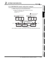
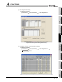
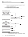
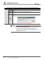
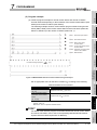
2.4 Checking the Function Version and Serial No.
This section explains how to check the function version and serial No. of the QJ71PB92V.
(1) Checking the "Rating plate" on the side of the module
The serial No. and function version of the module are printed in the SERIAL section of
the rating plate.
Serial No. (Upper 5 digits)
Function version
09052
D
Conformed standard
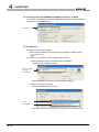
Figure 2.9 Rating Plate
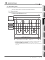
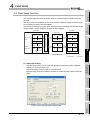
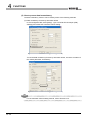
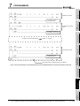
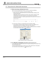
(2) Checking through GX Developer
The following explains how to check the serial No. and function version of the module
through GX Developer.
The serial No. and function version are displayed on the "Product information list" or
"Module's Detailed Information" screen of GX Developer.
The procedure for checking the serial No. and function version on the "Product
information list" screen is shown below.
Start Procedure
[Diagnostics]
[System monitor]
[Product inf. list]
Figure 2.10 Product Information List
2 - 14
2.4 Checking the Function Version and Serial No.
SYSTEM CONFIGURATION
* 1 The Product No. is displayed in the column only when the Universal model QCPU is used.
POINT
The serial No. shown on the rating plate may not match with the one displayed on
Product information list of GX Developer.
• The serial No. on the rating plate indicates the management information
of the product.
• The serial No. displayed on Product inf. list of GX Developer indicates the
functional information of the product.
The functional information of the product is updated when a new function
is added.
2
SYSTEM
CONFIGURATION
"Product No." column. *1
Note that "-" is displayed in the "Product No." column for the QJ71PB92V since
this module is not supporting Product No. display.
3
SPECIFICATIONS
[Serial No., Ver., Product No.]
• The serial No. of the module is displayed in the "Serial No." column.
• The function version of the module is displayed in the "Ver." column.
• The serial No. (Product No.) shown on the rating plate is displayed in the
OVERVIEW
1
FUNCTIONS
4
PROCEDURES AND
SETTINGS BEFORE
SYSTEM OPERATION
5
PARAMETER SETTING
6
PROGRAMMING
7
8
2.4 Checking the Function Version and Serial No.
2 - 15
DEDICATED
INSTRUCTIONS
2
3
SPECIFICATIONS
CHAPTER3 SPECIFICATIONS
This chapter explains the performance and transmission specifications of the QJ71PB92V.
For details of the general specifications, refer to the QCPU User's Manual (Hardware
Design, Maintenance and Inspection).
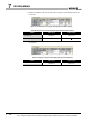
3.1 Performance Specifications
The performance specifications of the QJ71PB92V are given below.
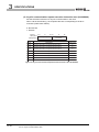
Table3.1 Performance Specifications
Item
Specifications
PROFIBUS-DP station type
DP-Master (Class 1)
Transmission specifications
Electrical standard/
characteristics
EIA-RS485 compliant
Medium
Shielded twisted pair cable (
Network topology
Bus topology (Tree topology when repeaters are used)
Data link method
Section 5.5.1)
• Between DP-Master and DP-Master: Token passing method
• Between DP-Master and DP-Slave:
Polling method
Encoding method
NRZ
Transmission speed *1
9.6 kbps to 12 Mbps (
Transmission distance
Differs depending on the transmission speed(
Max. No. of repeaters
3 repeaters
(1) in this section)
(1) in this section)
Number of connectable
modules
32 per segment (including repeater(s))
(Per segment)
Number of connectable
modules
126 per network (total of DP-Masters and DP-Slaves (
Section 2.2))
(Per network)
Max. No. of DP-Slaves *2
(Per QJ71PB92V)
125 per QJ71PB92V (
Section 2.2)
I/O data
Input data
size
Output data Max. 8192 bytes (Max. 244 bytes per DP-Slave)
Number of writes to flash
ROM
No. of occupied I/O points
Internal current consumption
(5VDC)
Max. 8192 bytes (Max. 244 bytes per DP-Slave)
Max. 100000 times
32 (I/O assignment: 32 intelligent points)
0.57 A
External dimensions
98(3.86 in.) (H) x 27.4(1.08 in.) (W) x 90(3.54 in.) (D) [mm]
Weight
0.13 kg
* 1 The transmission speed is controlled within
0.2%. (Compliant with IEC 61158-2)
* 2 Up to 124 when the QJ71PB92V is mounted to a redundant system. (
3-1
3.1 Performance Specifications
Section 2.3)
SPECIFICATIONS
1
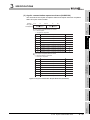
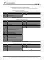
Table3.2 Transmission Distance
Transmission Speed
Transmission Distance
Max. Transmission Distance when
Repeater is Used *1
2
9.6 kbps
19.2 kbps
1200 m (3937 ft.)/segment
4800 m (15748 ft.)/network
187.5 kbps
1000 m (3281 ft.)/segment
4000 m (13123 ft.)/network
500 kbps
400 m (1312 ft.)/segment
1600 m (5249 ft.)/network
1.5 Mbps
200 m (656 ft.)/segment
800 m (2625 ft.)/network
100 m (328 ft.)/segment
400 m (1312 ft.)/network
SYSTEM
CONFIGURATION
93.75 kbps
3 Mbps
6 Mbps
OVERVIEW
(1) Transmission distance
3
* 1 The max. transmission distance in the table above is based on the case where 3 repeaters are
used.
The calculation formula for the transmission distance extended using a repeater(s) is:
Max. transmission distance [m/network] =
(Number of repeaters + 1) x Transmission distance [m/segment]
SPECIFICATIONS
12 Mbps
FUNCTIONS
4
PROCEDURES AND
SETTINGS BEFORE
SYSTEM OPERATION
5
PARAMETER SETTING
6
PROGRAMMING
7
8
3.1 Performance Specifications
3-2
DEDICATED
INSTRUCTIONS
3
3
SPECIFICATIONS
3.2 Function List
The following table summarizes a list of QJ71PB92V functions.
Table3.3 Function List
Function
Description
Reference
Section
PROFIBUS-DPV0
Up to 125 DP-Slaves can be connected to a single QJ71PB92V, enabling the I/O data
I/O data exchange
exchange of max. 8192 bytes.
Note that it is limited up to 124 DP-Slaves when the QJ71PB92V is used in a redundant
Section 4.1.1
system.
Acquisition of
diagnostic and
extended diagnostic
information
Global control function
Diagnostic or extended diagnostic information of an error occurred on a DP-Slaves
during I/O data exchange can be easily acquired using the buffer memory and I/O
Section 4.1.2
signals.
By sending services (SYNC, UNSYNC, FREEZE, UNFREEZE) to each DP-Slave in a
group, synchronous control of DP-Slave I/O data is available.
Section 4.1.3
PROFIBUS-DPV1
Acyclic communication
This function allows data reading/writing to DP-Slaves at any specific timing
with DP-Slaves
independently of I/O data exchange.
Alarm acquisition
This function enables acquisition of up to 8 alarms or status information data that have
been generated on any DP-Slave.
Support of FDT/DTM
Using a commercially available FDT, reading/writing the DP-Slave parameters and
technology
monitoring the DP-Slave status are executable via the QJ71PB92V.
Section 4.2.1
Section 4.2.2
Section 4.2.3
PROFIBUS-DPV2
Time control over DP-
This function allows the QJ71PB92V to operate as the time master and set the time of
Slaves
each DP-Slave.
Data swap function
This function swaps the upper and lower bytes in word units when I/O data is sent and
received.
Section 4.3.1
Section 4.4
When I/O data from DP-Slaves are read from or written to the buffer memory, this
Data consistency function
function prevents the I/O data from being separated and incorrectly mixed.
• Automatic refresh setting (GX Configurator-DP)
Section 4.5
• Dedicated instructions (BBLKRD and BBLKWR instructions)
This function sets whether to stop or continue I/O data exchange with DP-Slaves when a
Output status setting for the
case of a CPU stop error
CPU stop error occurs on a QCPU or remote I/O station where the QJ71PB92V is
mounted.
Section 4.6
When the QJ71PB92V is mounted to a redundant system, I/O data exchange with DPSlaves is continued regardless of the setting until systems A and B go down.
Temporary slave
Without modifying the slave parameter in GX Configurator-DP, this function allows the
reservation function
DP-Slave station type to be changed to "Reserved station" temporarily.
Redundant system support
When the control system CPU or the QJ71PB92V detects an error, the control and
function
standby systems are switched each other to continue communications.
QJ71PB92D-compatible
function
3-3
Section 4.7
Section 4.8
This function is used to replace the QJ71PB92D with the QJ71PB92V.
When the QJ71PB92D has failed, replace it with the QJ71PB92V using the
QJ71PB92D-compatible function.
3.2 Function List
Section 4.9
3
SPECIFICATIONS
1
OVERVIEW
3.3 Input/Output Signals to/from Programmable Controller CPU
This section explains the input/output signals of the QJ71PB92V.
3.3.1 List of I/O signals
The following I/O signal assignment is based on the case where the start I/O No. of the
QJ71PB92V is "0000" (installed to slot 0 of the main base unit).
Device X represents input signals from the QJ71PB92V to the QCPU. Device Y represents
output signals from the QCPU to the QJ71PB92V.
The following shows the I/O signals to/from the QCPU.
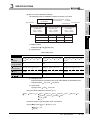
QCPU
Signal Name
Signal Direction: QCPU
Device No.
QJ71PB92V
Signal Name
X00
Data exchange start completed signal
Y00
X01
Diagnostic information detection signal
Y01
X02
Diagnostic information area cleared signal
Y02
Diagnostic information area clear request signal
X03
Use prohibited
Y03
Use prohibited
X04
Global control completed signal
Y04
Global control request signal
Global control failed signal
Y05
Use prohibited
signal
X07
Y09
Y0C
Data consistency start request signal
Y0D
Restart request signal
Y0E
Y0F
X10
Operation mode signal
Y10
X11
Operation mode change completed signal
Y11
X12
Y12
X13
Y13
Y14
Use prohibited
Y15
X16
Use prohibited
6
Operation mode change request signal
PARAMETER SETTING
Use prohibited
X0F
X15
PROCEDURES AND
SETTINGS BEFORE
SYSTEM OPERATION
Y0B
Data consistency requesting signal
X0D
X14
5
Use prohibited
Y0A
X0B
X0E
signal
4
Y08
Use prohibited
X0A
X0C
Extended diagnostic information read request
Y07
X08
X09
Y06
signal
Use prohibited
Y16
X17
Y17
7
X18
Alarm read response signal
Y18
Alarm read request signal
X19
Time control start response signal
Y19
Time control start request signal
(To the next page)
PROGRAMMING
X06
Extended diagnostic information read response
Diagnostic information detection reset request
8
3.3 Input/Output Signals to/from Programmable Controller CPU
3.3.1 List of I/O signals
3-4
DEDICATED
INSTRUCTIONS
X05
Data exchange start request signal
FUNCTIONS
Signal Direction: QJ71PB92V
SPECIFICATIONS
3
Table3.4 List of I/O Signals
Device No.
SYSTEM
CONFIGURATION
2
3
SPECIFICATIONS
Table3.4 List of I/O Signals (Continued)
Signal Direction: QJ71PB92V
Device No.
QCPU
Signal Name
X1A
Use prohibited
Signal Direction: QCPU
Device No.
QJ71PB92V
Signal Name
Y1A
X1B
Communication READY signal
Y1B
X1C
Use prohibited
Y1C
X1D
Module READY signal
Y1D
X1E
Use prohibited
Y1E
X1F
Watchdog timer error signal
Y1F
Use prohibited
POINT
Among the I/O signals for the QCPU, do not output (turn ON) the signals indicated
as "Use prohibited."
If any of the "Use prohibited" signals is output, the programmable controller
system may malfunction.
Remark
For how to use the output signals to continue or reexecute respective functions in
event of system switching in the redundant system, refer to Section 7.9.
3-5
3.3 Input/Output Signals to/from Programmable Controller CPU
3.3.1 List of I/O signals
SPECIFICATIONS
1
(b) When I/O data exchange is started after turning ON the Data exchange start
request signal (Y00), the Data exchange start completed signal (X00) turns ON.
The Data exchange start completed signal (X00) turns OFF in any of the following
cases:
• When the Data exchange start request signal (Y00) is turned OFF
• When an error causing stop of I/O data exchange occurs
• When parameters are currently being written to the QJ71PB92V from GX
Configurator-DP
• When the operation mode of the QJ71PB92V has been changed
• When a communication error has occurred on a DP-Slave.(Only when the
master parameter, "Error action flag" is checked)
Data exchange start request
Data exchange start
request signal (Y00)
2
SYSTEM
CONFIGURATION
(a) Turn ON the Data exchange start request signal (Y00) to start I/O data exchange.
3
SPECIFICATIONS
(1) Data exchange start request signal (Y00), data exchange start completed
signal (X00)
OVERVIEW
3.3.2 Details of I/O signals
4
Data exchange start
completed
I/O data exchange
stopped
Figure 3.1 Data Exchange Start Request Signal (Y00), Data Exchange Start Completed Signal (X00)
(c) Use these signals as interlock signals when reading/writing I/O data.
(d) Write the initial values of the output data to the buffer memory before turning ON
the Data exchange start request signal (Y00).
(e) Turning OFF the Data exchange start request signal (Y00) clears the information
in the following areas.
The information in the other buffer memory areas is held.
• Slave status area (Normal communication detection) (Un\G23040 to
Un\G23047)
• Slave status area (Diagnostic information detection) (Un\G23056 to
Un\G23064)
5
PROCEDURES AND
SETTINGS BEFORE
SYSTEM OPERATION
Exchanging I/O data
6
PARAMETER SETTING
I/O data exchange
stopped
FUNCTIONS
Data exchange start
completed signal (X00)
PROGRAMMING
7
8
3.3 Input/Output Signals to/from Programmable Controller CPU
3.3.2 Details of I/O signals
3-6
DEDICATED
INSTRUCTIONS
3
3
SPECIFICATIONS
(2) Diagnostic information detection reset request signal (Y01), Diagnostic
information detection signal (X01)
(a) The Diagnostic information detection signal (X01) turns ON when a
communication error is detected after the time preset in Diagnostic information
non-notification time setting area (Un\G2084) has elapsed.
The following processing is performed at the same time that the Diagnostic
information detection signal (X01) turns ON:
• The RSP ERR. LED turns ON.
• The diagnostic information is stored in the Diagnostic information area (for
mode 3) (Un\G23072 to Un\G23321).
The extended diagnostic information is stored in the Extended diagnostic
information area (for mode 3) (Un\G23328 to Un\G23454).
• The corresponding bit in the Slave status area (Diagnostic information
detection) (Un\G23056 to Un\G23064) of the station that sent the diagnostic
information turns ON.
• The error information of the QJ71PB92V is stored in the Local station error
information area (Un\G23071).
(b) Turning ON the Diagnostic information detection reset request signal (Y01) turns
OFF the Diagnostic information detection signal (X01).
The following processing is performed at the same time that the Diagnostic
information detection signal (X01) turns OFF:
• The RSP ERR. LED turns OFF.
• The corresponding bit in the slave status area (Diagnostic information
detection) (Un\G23056 to Un\G23064) of the station that sent the diagnostic
information turns ON.
(c) When new diagnostics information is generated while the Diagnostic information
detection reset request signal (Y01) is ON, the behavior is as follows:
• The Diagnostic information detection signal (X01) does not turn ON.
• The RSP ERR. LED does not turn ON.
• The corresponding bit in the Slave status area (Diagnostic information
detection) (Un\G23056 to Un\G23064) of the station that sent the diagnostic
information does not turn ON.
(d) After the Diagnostic information detection signal (X01) turns OFF, take actions for
the error cause and turn OFF the Diagnostic information detection reset request
signal (Y01).
3-7
3.3 Input/Output Signals to/from Programmable Controller CPU
3.3.2 Details of I/O signals
SPECIFICATIONS
(e) After the Diagnostic information detection signal (X01) is turned OFF, the
QJ71PB92V checks for diagnostic information again.
If any diagnostic information has been generated, the Diagnostic information
detection signal (X01) turns ON, and processing at (a) is performed.
2
MOV/FROM
instruction
Figure 3.2 Diagnostic Information Detection Reset Request Signal (Y01), Diagnostic Information
Detection Signal (X01)
Remark
4
5
PROCEDURES AND
SETTINGS BEFORE
SYSTEM OPERATION
Turning ON the Diagnostic information detection reset request signal (Y01) does
not clear the information shown below.
To clear the following information, turn ON the Diagnostic information area clear
request signal (Y02).
• Diagnostic information area (for mode 3) (Un\G23072 to Un\G23321)
• Extended diagnostic information area (for mode 3) (Un\G23328 to Un\G23454)
• Local station error information area (Un\G23071)
SPECIFICATIONS
3
1 Diagnostic information area (for mode 3) (Un\G23072 to Un\G23321)
Extended diagnostic information area (for mode 3) (Un\G23328 to Un\G23454)
Local station error information area (Un\G23071)
FUNCTIONS
1
SYSTEM
CONFIGURATION
Diagnostic information
Diagnostic information detection detection reset
reset request signal (Y01)
Diagnostic information Error detection
detection signal (X01)
Reads diagnostic, extended
diagnostic or local station error
information from buffer memory.
OVERVIEW
1
PARAMETER SETTING
6
PROGRAMMING
7
8
3.3 Input/Output Signals to/from Programmable Controller CPU
3.3.2 Details of I/O signals
3-8
DEDICATED
INSTRUCTIONS
3
3
SPECIFICATIONS
(3) Diagnostic information area clear request signal (Y02), Diagnostic
information area cleared signal (X02)
(a) Turn ON the Diagnostic information area clear request signal (Y02) when clearing
the following information:
• Diagnostic information area (for mode 3) (Un\G23072 to Un\G23321)
• Extended diagnostic information area (for mode 3) (Un\G23328 to
Un\G23454)
• Local station error information area (Un\G23071)
(b) When the Diagnostic information area clear request signal (Y02) is turned ON,
and the processing at (a) is completed, the Diagnostic information area cleared
signal (X02) turns ON.
(c) When new diagnostics information is generated while the Diagnostic information
area clear request signal (Y02) is ON, the following information stays cleared. (No
diagnostic, extended diagnostic or local station error information is stored.)
• Diagnostic information area (for mode 3) (Un\G23072 to Un\G23321)
• Extended diagnostic information area (for mode 3) (Un\G23328 to
Un\G23454)
• Local station error information area (Un\G23071)
(d) After the Diagnostic information area cleared signal (X02) has turned ON, turn
OFF the Diagnostic information area clear request signal (Y02).
(e) Taking corrective actions for the error and turning OFF the Diagnostic information
area clear request signal (Y02) turns OFF the Diagnostic information area cleared
signal (X02).
(f) After the Diagnostic information area clear request signal (Y02) is turned OFF, the
QJ71PB92V checks for diagnostic information again.
If any diagnostic information has been generated, the diagnostic information,
extended diagnostic information and/or local station error information is stored in
the buffer memory.
Diagnostic information area
clear request signal (Y02)
Diagnostic information area
cleared signal (X02)
Clear request
Clear completed
Figure 3.3 Diagnostic Information Area Clear Request Signal (Y02), Diagnostic Information Area Cleared
Signal (X02)
3-9
3.3 Input/Output Signals to/from Programmable Controller CPU
3.3.2 Details of I/O signals
SPECIFICATIONS
(b) When the Global control request signal (Y04) is turned ON, and global control
processing is completed, the Global control completed signal (X04) turns ON.
(c) After the Global control completed signal (X04) has turned ON, turn OFF the
Global control request signal (Y04).
(d) Turning OFF the Global control request signal (Y04) turns OFF the Global control
completed signal (X04).
(e) Turn ON the Global control request signal (Y04) while the Data exchange start
completed signal (X00) is ON.
If the Global control request signal (Y04) is turned ON with the Data exchange
start completed signal (X00) OFF, both of the Global control completed signal
(X04) and Global control failed signal (X05) turn ON.
2
SYSTEM
CONFIGURATION
(a) Turn ON the Global control request signal (Y04) when executing the global
control.
3
SPECIFICATIONS
(4) Global control request signal (Y04), Global control completed signal
(X04)
OVERVIEW
1
4
Output data is written.
1
FUNCTIONS
Data exchange start completed
signal (X00)
Writing of
output data
5
PROCEDURES AND
SETTINGS BEFORE
SYSTEM OPERATION
Global control request signal (Y04)
Global control completed signal (X04)
1 Output data area (for mode 3) (Un\G14336 to Un\G18431)
Figure 3.4 Global Control Request Signal (Y04), Global Control Completed Signal (X04)
PARAMETER SETTING
6
PROGRAMMING
7
8
3.3 Input/Output Signals to/from Programmable Controller CPU
3.3.2 Details of I/O signals
3 - 10
DEDICATED
INSTRUCTIONS
3
3
SPECIFICATIONS
(5) Global control failed signal (X05)
(a) If the Global control request signal (Y04) is turned ON while the Data exchange
start completed signal (X00) is OFF, both the Global control completed signal
(X04) and Global control failed signal (X05) turn ON.
(b) The ON status of the Global control failed signal (X05) means that the global
control has failed.
Remedy the cause of the error, and execute the global control again.
(c) Turning OFF the Global control request signal (Y04) turns OFF the Global control
failed signal (X05).
Global control request
Global control request signal (Y04)
Global control completed signal (X04)
Global control failed signal (X05)
Global control completed
Global control failed
Figure 3.5 Global Control Failed Signal (X05)
Remark
For details on the global control, refer to Section 4.1.3.
3 - 11
3.3 Input/Output Signals to/from Programmable Controller CPU
3.3.2 Details of I/O signals
SPECIFICATIONS
(b) Turning ON the Extended diagnostic information read request signal (Y06) clears
the information of the Extended diagnostic information read response area
(Un\G23457 to Un\G23583).
(c) When the Extended diagnostic information read request signal (Y06) is turned
ON, and reading of the extended diagnostic information of the specified FDL
address is completed, the Extended diagnostic information read response signal
(X06) turns ON.
(d) After the Extended diagnostic information read response signal (X06) has turned
ON, turn OFF the Extended diagnostic information read request signal (Y06).
(e) Turning OFF the Extended diagnostic information read request signal (Y06) turns
OFF the Extended diagnostic information read response signal (X06).
3
4
FUNCTIONS
Extended diagnostic
Extended diagnostic
information read request
information read request
signal (Y06)
Extended diagnostic information
read completed
Extended diagnostic
information read response
signal (X06)
2
SYSTEM
CONFIGURATION
(a) Turn ON the Extended diagnostic information read request signal (Y06) when
reading the extended diagnostic information of the FDL address specified in the
Extended diagnostic information read request area (Un\G23456).
SPECIFICATIONS
(6) Extended diagnostic information read request signal (Y06), Extended
diagnostic information read response signal (X06)
OVERVIEW
1
For details on acquisition of extended diagnostics information, refer to Section
4.1.2.
6
PARAMETER SETTING
Remark
PROCEDURES AND
SETTINGS BEFORE
SYSTEM OPERATION
5
Figure 3.6 Extended Diagnostic Information Read Request Signal (Y06), Extended Diagnostic Information
Read Response Signal (X06)
PROGRAMMING
7
8
3.3 Input/Output Signals to/from Programmable Controller CPU
3.3.2 Details of I/O signals
3 - 12
DEDICATED
INSTRUCTIONS
3
3
SPECIFICATIONS
(7) Data consistency start request signal (Y0C), Data consistency
requesting signal (X0C)
(a) The Data consistency start request signal (Y0C) is used to enable the data
consistency function for dedicated instructions.
Table3.5 Data Consistency Start Request Signal (Y0C)
ON/OFF Status
Description
Enables read/write executed by dedicated instructions.
Turning ON the Data consistency start request signal
ON
(Y0C) turns ON the Data consistency requesting
signal (X0C).
Disables read/write executed by dedicated
instructions.
Turning OFF the Data consistency start request signal
OFF
(Y0C) turns OFF the Data consistency requesting
signal (X0C), and the BBLKRD and BBLKWR
instructions are not executed.
(b) Use the Data consistency start request signal (Y0C) and Data consistency
requesting signal (X0C) as interlock signals for dedicated instructions.
(c) When using the data consistency function (automatic refresh) by the GX
Configurator-DP, turn OFF the Data consistency start request signal (Y0C).
Data consistency start
request signal (Y0C)
Data consistency
start request
Data consistency
requesting signal (X0C)
Data consistency
function enabled
Figure 3.7 Data Consistency Start Request Signal (Y0C), Data Consistency Requesting Signal (X0C)
(8) Restart request signal (Y0D)
(a) If the QJ71PB92V has gone down for some reason (the FAULT LED: ON, the
module READY signal (X1D): OFF), turning the Restart request signal (Y0D) OFF,
ON and OFF again restarts the QJ71PB92V.
(b) After the QJ71PB92V is restarted, the status is the same as the one after:
• The programmable controller is turned OFF and back ON again.
• The QCPU is reset.
(9) Operation mode signal (X10)
This signal indicates whether or not the current operation mode is Communication
mode (mode 3).
Table3.6 Operation Mode Signal (X10)
ON/OFF Status
3 - 13
Description
ON
Other than Communication mode (mode 3)
OFF
Communication mode (mode 3)
3.3 Input/Output Signals to/from Programmable Controller CPU
3.3.2 Details of I/O signals
SPECIFICATIONS
(b) Turning ON the Operation mode change request signal (Y11) clears the
information of the Operation mode change result area (Un\G2256).
(c) The Operation mode change completed signal (X11) turns ON when the operation
mode is changed, and the result of the change is stored to the Operation mode
change result area (Un\G2256).
(d) Make sure that A300H (Normally completed) is stored in the Operation mode
change result area (Un\G2256), and turn OFF the Operation mode change
request signal (Y11).
(e) Turning OFF the Operation mode change request signal (Y11) turns OFF the
Operation mode change completed signal (X11).
2
SYSTEM
CONFIGURATION
(a) Turn ON the Operation mode change request signal (Y11) when changing the
operation mode to the one set in the Operation mode change request area
(Un\G2255).
The operation mode can be changed without resetting the QCPU.
3
SPECIFICATIONS
(10) Operation mode change request signal (Y11), Operation mode change
completed signal (X11)
OVERVIEW
1
4
Data exchange start request signal : Y00
FUNCTIONS
Operation mode change request signal : Y11
Operation mode change completed signal : X11
MOV/TO
instruction
MOV/FROM
instruction
Check the result in "Operation
Set an operation mode in
mode change result area" and
"Operation mode change
"Current operation mode".
request area".
Figure 3.8 Operation mode change request signal (Y11), Operation mode change completed signal (X11)
POINT
(1) Do not turn the power OFF or reset the QCPU during the operation mode
registration to the flash ROM by turning ON the Operation mode change request
signal (Y11).
Turn the power OFF or reset the QCPU after the Operation mode change
completed signal (X11) has turned ON.
If the power is turned OFF or the QCPU is reset by mistake, register the operation
mode to the flash ROM again.
(2) If the redundant CPU is in the Backup mode, the operation mode of the
QJ71PB92V cannot be changed.
An error code is stored in the Operation mode change result area (Un\G2256).
(
Section 9.5.2)
The operation mode of the QJ71PB92V must be changed when the redundant
CPU is in Separate or Debug mode. (
QnPRHCPU User's Manual
(Redundant System))
3.3 Input/Output Signals to/from Programmable Controller CPU
3.3.2 Details of I/O signals
3 - 14
6
PARAMETER SETTING
Operation mode change result
7
PROGRAMMING
Operation mode change result area (Un\G2256)
PROCEDURES AND
SETTINGS BEFORE
SYSTEM OPERATION
5
8
DEDICATED
INSTRUCTIONS
3
3
SPECIFICATIONS
(11) Alarm read request signal (Y18), Alarm read response signal (X18)
(a) Turn ON the Alarm read request signal (Y18) when reading alarms on the
specified DP-Slave according to the information set in the Alarm request area
(Un\G26432 to Un\G26434).
(b) Turning ON the Alarm read request signal (Y18) clears the information in the
Alarm response area (Un\G26446 to Un\G26768).
Note, however, that the information in the following areas are not cleared when
the alarm ACK request (request code: 1501H) is executed:
Table3.7 Areas Not Cleared At Alarm ACK Request Execution
Buffer Memory Address
Description
DEC (HEX)
26449 to 26484
(6751H to 6774H)
26489 to 26524
(6779H to 679CH)
26529 to 26564
(67A1H to 67C4H)
26569 to 26604
(67C9H to 67ECH)
26609 to 26644
(67F1H to 6814H)
26649 to 26684
(6819H to 683CH)
26689 to 26724
(6841H to 6864H)
26729 to 26764
(6869H to 688CH)
Area to which alarm data of alarm data No.1 is stored
Area to which alarm data of alarm data No.2 is stored
Area to which alarm data of alarm data No.3 is stored
Area to which alarm data of alarm data No.4 is stored
Area to which alarm data of alarm data No.5 is stored
Area to which alarm data of alarm data No.6 is stored
Area to which alarm data of alarm data No.7 is stored
Area to which alarm data of alarm data No.8 is stored
(c) The Alarm read response signal (X18) turns ON when alarms on the specified
DP-Slave are read, and the execution result is stored to the Alarm response area
(Un\G26446 to Un\G26768).
(d) Read the alarm information from the Alarm response area (Un\G26446 to
Un\G26768), and turn OFF the Alarm read request signal (Y18).
(e) Turning OFF the Alarm read request signal (Y18) turns OFF, the Alarm read
response signal (X18).
Remark
For details on acquisition of alarms, refer to Section 4.2.2.
3 - 15
3.3 Input/Output Signals to/from Programmable Controller CPU
3.3.2 Details of I/O signals
SPECIFICATIONS
(b) Turning ON the Time control start request signal (Y19) clears the information in
the Time control setting response area (Un\G26800 to Un\G26812).
(c) The Time control start response signal (X19) turns ON when the time control over
DP-Slaves is executed, and the execution result is stored in the Time control
setting response area (Un\G26800 to Un\G26812).
(d) Read the execution result from the Time control setting response area
(Un\G26800 to Un\G26812), and turn OFF the Time control start request signal
(Y19).
(e) Turning OFF the Time control start request signal (Y19) turns OFF the Time
control start response signal (X19).
2
SYSTEM
CONFIGURATION
(a) Turn ON the Time control start request signal (Y19) when executing the time
control over DP-Slaves according to the information set in the Time control setting
request area (Un\G26784 to Un\G26792).
3
SPECIFICATIONS
(12) Time control start request signal (Y19), Time control start response
signal (X19)
OVERVIEW
1
4
Remark
FUNCTIONS
For details on time control over DP-Slaves, refer to Section 4.3.1.
(c) Use the signal as an interlock signal for when turning ON the Data exchange start
request signal (Y00).
(14) Module READY signal (X1D)
(a) This signal turns ON when the QJ71PB92V is started up. (This signal turns ON
regardless of the operation mode.)
(b) While the QJ71PB92V is not ready, this signal is OFF.
(15) Watchdog timer error signal (X1F)
(a) This signal turns ON when a watchdog timer error occurs on the QJ71PB92V.
(b) The Watchdog timer error signal (X1F) does not turn OFF until:
• The programmable controller is turned OFF and back ON again, or
• The QCPU is reset.
3.3 Input/Output Signals to/from Programmable Controller CPU
3.3.2 Details of I/O signals
PROCEDURES AND
SETTINGS BEFORE
SYSTEM OPERATION
(b) The signal turns OFF when an error disabling I/O data exchange occurs on the
QJ71PB92V.
5
6
PARAMETER SETTING
(a) The Communication READY signal (X1B) turns ON when the Module READY
signal (X1D) turns ON and I/O data exchange is ready to be started. (The signal
turns ON only in the Communication mode (mode 3).)
7
PROGRAMMING
(13) Communication READY signal (X1B)
8
3 - 16
DEDICATED
INSTRUCTIONS
3
3
SPECIFICATIONS
3.4 Buffer Memory
This section explains the buffer memories of the QJ71PB92V.
3.4.1 Buffer memory list
The following shows a list of the buffer memories that are used for transferring data
between the QJ71PB92V and the QCPU.
Table3.8 Buffer Memory List
Address
Name
DEC (HEX)
0 to 2079
2080
(820H)
2081
(821H)
2082 to 2083
(822H to 823H)
2084
(824H)
2085
(825H)
2086 to 2253
(826H to 8CDH)
2254
(8CEH)
2255
(8CFH)
2256
(8D0H)
2257
(8D1H)
2258
(8D2H)
2259
(8D3H)
2260 to 2262
(8D4H to 8D6H)
(8D7H)
2264
(8D8H)
Initial
Read/
Reference
value
Write*1
Section
System area (Use prohibited)
(0H to 81FH)
2263
Description
Diagnostic information invalid
setting area
Values for masking (invalidating) diagnostic
information from DP-Slaves are set in this
area.
02B9H
R/W
Section
3.4.6
Global control area
The global control function to be executed is
set in this area.
0
R/W
Section
3.4.9
Diagnostic information nonnotification time setting area
This area is used to set the time during which
no diagnostic information is notified after
communication start.
20
R/W
Section
3.4.6
Current diagnostic information
non-notification time area
This area stores the time (remaining time)
during which no diagnostic information is
notified after communication start.
0
R
Section
3.4.6
System area (Use prohibited)
System area (Use prohibited)
Current operation mode area
This area stores data of the currently operating
mode.
0001H
R
Section
3.4.2
Operation mode change request
area
When executing the operation mode change
request, a desired operation mode is set in this
area.
FFFEH
R/W
Section
3.4.3
Operation mode change result
area
This area stores the execution result of the
operation mode change request.
0
R
Section
3.4.3
Local FDL address display area
This area stores the FDL address of the local
station.
FFFFH
R
Section
3.4.2
Offline test status area
This area stores the details or result of the selfdiagnostic test.
0
R
Section
3.4.2
Flash ROM storage mode
This area stores the operation mode currently
stored in the flash ROM.
FFFFH
R
Section
3.4.2
Control master FDL address
display area
This area stores the FDL address of the
control system QJ71PB92V when it is used in
a redundant system.
*2
R
Section
3.4.14
Standby master FDL address
display area
This area stores the FDL address of the
standby system QJ71PB92V when it is used in
a redundant system.
*2
R
Section
3.4.14
System area (Use prohibited)
* 1 This indicates whether or not read/write is possible from the sequence program.
R: Read only, R/W: Read/write executable
* 2 The initial value varies depending on the QCPU installed with the QJ71PB92V or the parameter.
(
Section 3.4.14)
(To the next page)
3 - 17
3.4 Buffer Memory
3.4.1 Buffer memory list
3
SPECIFICATIONS
1
DEC (HEX)
2275 to 6143
(8E3H to 17FFH)
6144 to 10239
(1800H to 27FFH)
10240 to 14335
(2800H to 37FFH)
14336 to 18431
(3800H to 47FFH)
18432 to 22527
(4800H to 57FFH)
22528 to 22777
22778 to 22783
22784 to 22908
Current bus cycle time
Min. bus cycle time
Max. bus cycle time
22909 to 22911
22912 to 23036
(59FDH to 59FFH)
23040 to 23047
Input data area (for mode 3)
23065 to 23070
This area stores the minimum value of the bus
cycle time.
0
R
This area stores the maximum value of the bus
cycle time.
0
R
Section
3.4.8
Section
3.4.8
3
used to store the input data received from each
Section
0
R
0
R/W
FFFFH
R
3.4.4
In Communication mode (mode 3), this area is
Output data area (for mode 3)
used to set the output data to be sent to each
DP-Slave.
Section
3.4.4
Address information area
In Communication mode (mode 3), this area is
used to store the FDL address of each DPSlave and I/O data length.
Section
3.4.4
System area (Use prohibited)
Input data start address area
5
In Communication mode (mode 3), this area is
used to store the start address (buffer memory
0
R
0
R
address) of the input data of each DP-Slave.
Section
3.4.4
System area (Use prohibited)
Output data start address area
In Communication mode (mode 3), this area is
used to store the start address (buffer memory
address) of the output data of each DP-Slave.
Section
3.4.4
System area (Use prohibited)
Slave status area (Normal
Slave status area (Reserved
Slave status area (Diagnostic
This area stores the communication status of
each DP-Slave.
This area stores the reserved or temporary
slave reservation setting of each DP-Slave.
This area stores the diagnostic information
generation status of each DP-Slave.
0
0
R
R
0
R
0
R
0
R
Section
3.4.5
Section
3.4.5
Section
3.4.5
6
7
System area (Use prohibited)
23071
Local station error information
This area stores the error information of the
(5A1FH)
area
local station (QJ71PB92V).
Section
3.4.2
In Communication mode (mode 3), this area is
23072 to 23321
4
System area (Use prohibited)
(5A10H to 5A18H) information detection)
(5A19H to 5A1EH)
2
3.4.8
System area (Use prohibited)
(5A08H to 5A0FH) station setting status)
23056 to 23064
Section
DP-Slave.
(5A00H to 5A07H) communication detection)
23048 to 23055
R
In Communication mode (mode 3), this area is
(5980H to 59FCH) (for mode 3)
23037 to 23039
This area stores the current bus cycle time.
System area (Use prohibited)
(5900H to 597CH) (for mode 3)
(597DH to 597FH)
0
System area (Use prohibited)
(5800H to 58F9H) (for mode 3)
(58FAH to 58FFH)
Section
FUNCTIONS
2274
(8E2H)
Write*1
PROCEDURES AND
SETTINGS BEFORE
SYSTEM OPERATION
2273
(8E1H)
Reference
value
PARAMETER SETTING
2272
(8E0H)
Read/
Diagnostic information area
(5A20H to 5B19H) (for mode 3)
used to store the diagnostic information of the
error occurred on each DP-Slave during
Section
3.4.6
communication.
* 1 This indicates whether or not read/write is possible from the sequence program.
R: Read only, R/W: Read/write executable
(To the next page)
3.4 Buffer Memory
3.4.1 Buffer memory list
3 - 18
PROGRAMMING
(8D9H to 8DFH)
Initial
8
DEDICATED
INSTRUCTIONS
2265 to 2271
Description
SYSTEM
CONFIGURATION
Name
SPECIFICATIONS
Address
OVERVIEW
Table3.8 Buffer Memory List (Continued)
3
SPECIFICATIONS
Table3.8 Buffer Memory List (Continued)
Address
Name
DEC (HEX)
23322 to 23327
(5B1AH to 5B1FH)
Description
Initial
Read/
Reference
value
Write*1
Section
0
R
FFFFH
R/W
0
R
0
R
0
R
0
R
0
R/W
0
R/W
0
R
0
R/W
System area (Use prohibited)
In Communication mode (mode 3), this area is
23328 to 23454
Extended diagnostic information
(5B20H to 5B9EH) area (for mode 3)
used to store the extended diagnostic
information of the error occurred on each DP-
Section
3.4.6
Slave during communication.
23455
System area (Use prohibited)
(5B9FH)
23456
Extended diagnostic information
(5BA0H)
read request area
23457 to 23583
Extended diagnostic information
(5BA1H to 5C1FH) read response area
23584 to 23591
Parameter setting status area
(5C20H to 5C27H) (Active station)
23592 to 23599
Parameter setting status area
(5C28H to 5C2FH) (Reserved station)
23600 to 23607
Temporary slave reservation
(5C30H to 5C37H) status area
23608 to 23615
23616 to 23647
23648 to 23656
(5C60H to 5C68H)
23657 to 23663
(5C69H to 5C6FH)
23664 to 23672
(5C70H to 5C78H)
23673 to 23807
(5C79H to 5CFFH)
23808
(5D00H)
23809 to 24832
Temporary slave reservation
(6101H to 621FH)
This area stores the execution result of the
extended diagnostic information read request.
3.4.7
Section
3.4.5
parameters.
This area stores data of the DP-Slaves that are
set to Reserved station by the slave
Section
3.4.5
parameters.
This area stores data of the DP-Slaves that are
set to Temporary slave reservation by the
Section
3.4.5
This area is used to set DP-Slaves to
Temporary slave reservation using the
3.4.7
Section
This area stores data of the DP-Slaves that are
set to Normal DP-Slave by the slave
Section
Section
3.4.13
System area (Use prohibited)
System switching condition
When the QJ71PB92V is mounted on a
setting area (Disconnected
redundant system, this area is used to set the
station detection)
switching target DP-Slaves.
Section
3.4.14
System area (Use prohibited)
System switching condition
When the QJ71PB92V is mounted on a
setting result area (Disconnected redundant system, this area stores the
station detection)
Section
3.4.14
switching target DP-Slaves.
System area (Use prohibited)
Acyclic communication request
This area is used to set which request is to be
execution instruction area
executed in acyclic communications.
Acyclic communication request
This area is used to set the request data for
acyclic communications.
0
R/W
0
R
0
R
Section
3.4.10
Section
3.4.10
System area (Use prohibited)
25120
Acyclic communication request
(6220H)
result area
25121 to 26144
information is read.
temporary slave reservation function.
(5D01H to 6100H) area
24833 to 25119
station from which the extended diagnostic
temporary slave reservation function.
(5C38H to 5C3FH) request area
(5C40H to 5C5FH)
This area is used to set the FDL address of the
This area stores the request acceptance status
and execution completion status in acyclic
communications.
Acyclic communication response This area stores the execution result of acyclic
(6221H to 6620H) area
communication.
Section
3.4.10
Section
3.4.10
* 1 This indicates whether or not read/write is possible from the sequence program.
R: Read only, R/W: Read/write executable
(To the next page)
3 - 19
3.4 Buffer Memory
3.4.1 Buffer memory list
3
SPECIFICATIONS
1
Slave status area
26432 to 26434
(6740H to 6742H)
26435 to 26445
(6743H to 674DH)
26446 to 26768
(674EH to 6890H)
26769 to 26783
(6891H to 689FH)
26784 to 26792
(68A0H to 68A8H)
26793 to 26799
(68A9H to 68AFH)
26800 to 26812
(68BDH to 7FFFH)
Slave.
0
R
Section
2
0
R/W
0
R
0
R/W
3.4.5
System area (Use prohibited)
Alarm request area
This area is used to set the request data for
alarm acquisition.
Section
3.4.11
System area (Use prohibited)
Alarm response area
This area stores the execution result of alarm
acquisition.
Section
Time control setting request area
This area is used to set the request data for
time control.
Section
3.4.12
System area (Use prohibited)
Time control setting response
3
3.4.11
System area (Use prohibited)
(68B0H to 68BCH) area
26813 to 32767
This area stores the alarm status of each DP-
4
This area stores the execution result of time
control.
0
R
Section
3.4.12
System area (Use prohibited)
FUNCTIONS
26425 to 26431
Section
System area (Use prohibited)
(6730H to 6738H) (Alarm detection)
(6739H to 673FH)
Write*1
* 1 This indicates whether or not read/write is possible from the sequence program.
R : Read only, RW : Read/write executable
5
POINT
PROCEDURES AND
SETTINGS BEFORE
SYSTEM OPERATION
26416 to 26424
Reference
value
Do not write any data to "System area (Use prohibited)".
Doing so may cause the programmable controller system to malfunction.
6
PARAMETER SETTING
(6621H to 672FH)
Read/
7
PROGRAMMING
26145 to 26415
Initial
SYSTEM
CONFIGURATION
DEC (HEX)
Description
SPECIFICATIONS
Name
8
3.4 Buffer Memory
3.4.1 Buffer memory list
3 - 20
DEDICATED
INSTRUCTIONS
Address
OVERVIEW
Table3.8 Buffer Memory List (Continued)
3
SPECIFICATIONS
3.4.2 Local station information area
The information of the local station (QJ71PB92V) is stored in this area.
(1) Local station error information area (Un\G23071)
This area stores the error information of the local station (QJ71PB92V).
Table3.9 Local Station Error Information Area (Un\G23071)
Stored Value
0000H
Other than 0000H
Description
Normal
Error (Error code (
Section 9.5.6 ))
POINT
The information in the Local station error information area (Un\G23071) is not
cleared even if the problem occurred on the QJ71PB92V has been solved.
To clear the Local station error information area (Un\G23071), turn ON the
Diagnostic information area clear request signal (Y02).
(2) Current operation mode area (Un\G2254)
This area stores the current operation mode value.
Table3.10 Current Operation Mode Area (Un\G2254)
Stored Value
Description
0001H
Parameter setting mode
0002H
Self-diagnostic mode
0003H
Communication mode (mode 3)
0009H
Flash ROM clear mode
0101H
Parameter setting mode *1
0103H
Communication mode (mode 3) *1
* 1 Operation mode currently registered to flash ROM
(3) Flash ROM storage mode (Un\G2259)
This area stores the operation mode currently stored to flash ROM.
Table3.11 Flash ROM Storage Mode (Un\G2259)
Stored Value
3 - 21
Description
0101H
Parameter setting mode
0103H
Communication mode (mode 3)
FFFFH
Not registered (No operation mode has been registered to the flash ROM.)
3.4 Buffer Memory
3.4.2 Local station information area
SPECIFICATIONS
1
(4) Local FDL address display area (Un\G2257)
OVERVIEW
The FDL address of the local station is stored.
Table3.12 Local FDL Address Display Area (Un\G2257)
(0 to 125)
FFFFH
Description
2
The FDL address of the local station *1
Parameter not set
* 1 When the QJ71PB92V is mounted on a redundant system, the following address is stored.
When it is in the control system: Control master FDL address
When it is in the standby system: Standby master FDL address
SYSTEM
CONFIGURATION
Stored Value
0000H to 007DH
3
(5) Offline test status area (Un\G2258)
SPECIFICATIONS
The self-diagnostics test details or test result is stored in this area.
For details on the self-diagnostics test, refer to Section 5.4.
FUNCTIONS
4
PROCEDURES AND
SETTINGS BEFORE
SYSTEM OPERATION
5
PARAMETER SETTING
6
PROGRAMMING
7
8
3.4 Buffer Memory
3.4.2 Local station information area
3 - 22
DEDICATED
INSTRUCTIONS
3
3
SPECIFICATIONS
3.4.3 Operation mode change area
This area is used to change the operation mode of the local station (QJ71PB92V).
For changing the operation mode, refer to Section 6.2.
(1) Operation mode change request area (Un\G2255)
For execution of the operation mode change request, set a desired operation mode.
(Initial value: FFFEH)
The initial value (FFFEH) is used for malfunction prevention.
If the Operation mode change request signal (Y11) is turned ON with the initial value
stored in the Operation mode change request area (Un\G2255), E300H is stored in the
Operation mode change result area (Un\G2256) and the operation mode is not
changed.
Table3.13 Operation Mode Change Request Area (Un\G2255)
Set Value
Description
0001H
The mode is changed to Parameter setting mode.
0002H
The mode is changed to Self-diagnostics mode.
0003H
The mode is changed to Communication mode (mode 3).
0009H
The mode is changed to Flash ROM clear mode.
The mode is changed to Parameter setting mode.
The Parameter setting mode is registered to the flash ROM at the same
0101H
time as the operation mode change.
The mode is changed to Communication mode (mode 3).
The Communication mode (mode 3) is registered to the flash ROM at the
0103H
same time as the operation mode change.
The mode is changed to Parameter setting mode.
The mode registered to the flash ROM is deleted at the same time as the
FFFFH
operation mode change.
POINT
If the redundant CPU is in the Backup mode, the operation mode of the
QJ71PB92V cannot be changed.
An error code is stored in the Operation mode change result area (Un\G2256).
(
Section 9.5.2)
The operation mode of the QJ71PB92V must be changed when the redundant
CPU is in Separate or Debug mode. (
(Redundant System))
QnPRHCPU User's Manual
(2) Operation mode change result area (Un\G2256)
This area stores the execution result of the operation mode change request.
Table3.14 Operation Mode Change Result Area (Un\G2256)
Stored Value
3 - 23
Description
A300H
Normally completed
Other than A300H
Failed (Error code (
3.4 Buffer Memory
3.4.3 Operation mode change area
Section 9.5.2))
SPECIFICATIONS
1
OVERVIEW
3.4.4 I/O data exchange area
POINT
(1) Data are assigned to the I/O data exchange area in the order of parameters
set in GX Configurator-DP (in the order of FDL addresses).
The actual assignment order can be confirmed in the Address information
area (for mode 3) (Un\G22528 to Un\G22777) or in Slave List of GX
Configurator-DP.
2
SYSTEM
CONFIGURATION
This area is used for the I/O data exchange function.
3
Section 6.5)
*1,
(3) Input data of a DP-Slave which has failed in I/O data exchange, are not
stored in the Input data area of the QJ71PB92V.
Data stored before the fault are held in the relevant Input data area for the
DP-Slave.
* 1 DP-Slave corresponding to the bit that is turned OFF in the Slave status area (Normal
communication detection) (Un\G23040 to Un\G23047)
FUNCTIONS
need to check the sequence program. (
4
5
PROCEDURES AND
SETTINGS BEFORE
SYSTEM OPERATION
(2) When parameters have been modified (deletion or addition of DP-Slave(s))
on GX Configurator-DP, the buffer memory is reassigned.
After modifying parameters, review the sequence program.
If some DP-Slaves are expected to be connected to the network in the future,
setting them as Reserved stations in the parameter setting eliminates the
SPECIFICATIONS
Order of assignment
PARAMETER SETTING
6
PROGRAMMING
7
8
3.4 Buffer Memory
3.4.4 I/O data exchange area
3 - 24
DEDICATED
INSTRUCTIONS
3
3
SPECIFICATIONS
(1) Input data area (for mode 3) (Un\G6144 to Un\G10239)
When the operation mode is Communication mode (mode 3), input data from DPSlaves are stored in this area.
(a) Data length setting
The data length (unit: byte) for each station is variable and assigned based on the
slave parameter (Select Modules) set on GX Configurator-DP.
For the DP-Slave that has a fixed data length, the slave parameter (Select
Modules) setting is ignored.
(b) Data length range
The maximum data length per module is 244 bytes, and the total data length for all
DP-Slaves can be set up to 8192 bytes.
When the data length is an odd number of bytes, 00H is stored to the final high byte.
The input data of the next station is assigned starting from the next buffer memory
address.
Address
DEC (HEX)
6144(1800H)
to
b15
b8 b7
b0
6144(1800H) 2nd byte of 1st module
1st byte of 1st module
Input data of 1st module
(Input data length:
23 bytes)
6145(1801H) 4th byte of 1st module
3rd byte of 1st module
Input data of 2nd module
(Input data length:
7 bytes)
6155(180BH) 22nd byte of 1st module 21st byte of 1st module
6156(180CH)
6157(180DH)
to
6160(1810H)
to
6156(180CH)
00H
23rd byte of 1st module
6157(180DH) 2nd byte of 2nd module 1st byte of 2nd module
6158(180EH) 4th byte of 2nd module
3rd byte of 2nd module
6159(180FH) 6th byte of 2nd module
5th byte of 2nd module
6160(1810H)
7th byte of 2nd module
00H
Input data of n-th module
10239(27FFH)
Figure 3.9 Example of Input Data Assignment (1st module: 23 bytes, 2nd module: 7 bytes)
POINT
If a DP-Slave with no input data is assigned, its space in the input data area is
taken over by the next station with input data, as shown below.
Each DP-Slave setting
1st module
Input data : Set
2nd module
Input data : None
3rd module
Input data : Set
4th module
Input data : Set (Data length: 0)
Assignment result in Input data area of QJ71PB92V
6144(1800H)
Input data of 1st module
Input data of 3rd module
5th module
3 - 25
Input data : Set
3.4 Buffer Memory
3.4.4 I/O data exchange area
Input data of 5th module
Because of no input data setting for 2nd
and 4th modules, no area is assigned for them
SPECIFICATIONS
1
(b) Data length range
The maximum data length per module is 244 bytes, and the total data length for all
DP-Slaves can be set up to 8192 bytes.
When the data length is an odd number of bytes, the final high byte is occupied.
Set 00H to the final high byte.
The output data of the next station is assigned starting from the next buffer address.
b8 b7
b0
14336(3800H) 2nd byte of 1st module
1st byte of 1st module
Output data of 1st module
(Output data length:
23 bytes)
14337(3801H) 4th byte of 1st module
3rd byte of 1st module
Output data of 2nd module
(Output data length:
7 bytes)
14347(380BH) 22nd byte of 1st module 21st byte of 1st module
4
FUNCTIONS
to
b15
14348(380CH)
to
14352(3810H)
to
14348(380CH)
00H
23rd byte of 1st module
14349(380DH) 2nd byte of 2nd module
1st byte of 2nd module
14350(380EH) 4th byte of 2nd module
3rd byte of 2nd module
14351(380FH) 6th byte of 2nd module
5th byte of 2nd module
14352(3810H)
7th byte of 2nd module
00H
5
PROCEDURES AND
SETTINGS BEFORE
SYSTEM OPERATION
14349(380DH)
Output data of n-th module
18431(47FFH)
6
Figure 3.10 Example of Output Data Assignment (1st module: 23 bytes, 2nd module: 7 bytes)
POINT
If a DP-Slave with no output data is assigned, its space in the output data area is
taken over by the next station with output data, as shown below.
1st module
Output data : Set
2nd module
Output data : None
3rd module
Output data : Set
4th module
Output data : Set (Data length: 0)
Assignment result in Output data area of QJ71PB92V
14336(3800H)
Output data of 1st module
Output data of 3rd module
5th module
Output data : Set
Output data of 5th module
Because of no output data setting for 2nd
and 4th modules, no area is assigned for them
3.4 Buffer Memory
3.4.4 I/O data exchange area
7
PROGRAMMING
Each DP-Slave setting
3
PARAMETER SETTING
Address
DEC (HEX)
14336(3800H)
2
SYSTEM
CONFIGURATION
(a) Data length setting
The data length (unit: byte) of each station is variable and assigned based on the
slave parameter (Select Modules) set on GX Configurator-DP.
For the DP-Slave that has a fixed data length, the slave parameter (Select
Modules) setting is ignored.
SPECIFICATIONS
When the operation mode is Communication mode (mode 3), output data to DPSlaves are set.
OVERVIEW
(2) Output data area (for mode 3) (Un\G14336 to Un\G18431)
3 - 26
8
DEDICATED
INSTRUCTIONS
3
3
SPECIFICATIONS
(3) Address information area (for mode 3) (Un\G22528 to Un\G22777)
When the operation mode is Communication mode (mode 3), the FDL address and
I/O data length of each DP-Slave are stored in this area.
Information of 125 modules is stored in the Address information area (for mode 3) in
the same order for each module.
Information for reserved or temporary slave reservation is also stored.
Address
DEC (HEX)
22528(5800H)
FDL address of 1st module
22529(5801H)
I/O data length of 1st module
22530(5802H)
FDL address of 2nd module
22531(5803H)
I/O data length of 2nd module
b15
to
22776(58F8H)
FDL address of 125th module
22777(58F9H) I/O data length of 125th module
b8 b7
22528(5800H)
0000H to 007DH (0 to 125): FDL address
FFFFH
: No FDL address assigned
The input data length of the 1st The output data length of the 1st
module is stored. (Initial value: module is stored. (Initial value:
FFH) *1
FFH) *1
22529(5801H)
00H to F4H : Input data
00H to F4H : Output data
length
length
(unit: byte)
(unit: byte)
FFH : Input data not assigned
FFH : Output data not assigned
Figure 3.11 Address Information Area (for mode 3) (Un\G22528 to Un\G22777)
* 1 The difference between 00H and FFH is as follows:
00H means that input or output data are assigned with the data length set to 0.
FFH shows that assigned input or output data do not exist.
3 - 27
3.4 Buffer Memory
3.4.4 I/O data exchange area
b0
The FDL address of the 1st module is stored. (Initial value: FFFFH)
3
SPECIFICATIONS
1
22785(5901H) Input data start address of 2nd module
to
b15
b0
The start address (buffer memory address) of the
input data of the 1st module is stored. (Initial value:
FFFFH)
22528(5800H)
1800H to 27FFH : Input data start address
FFFFH
: Input data not assigned
22908(597CH) Input data start address of 125th module
SYSTEM
CONFIGURATION
Address
DEC (HEX)
22784(5900H) Input data start address of 1st module
2
3
SPECIFICATIONS
When the operation mode is Communication mode (mode 3), the start address (buffer
memory address) for each DP-Slave's input data is stored in this area.
Creating a sequence program utilizing the Input data start address area (for mode 3)
(Un\G22784 to Un\G22908) allows address specification of the Input data area
without consideration of the input points for each DP-Slave.
Information of 125 modules is stored in the Input data start address area (for mode 3)
in the same order for each module.
OVERVIEW
(4) Input data start address area (for mode 3) (Un\G22784 to Un\G22908)
4
Figure 3.12 Input Data Start Address Area (for mode 3) (Un\G22784 to Un\G22908)
22913(5981H) Output data start address of 2nd module
to
b0
The start address (buffer memory address) of the
output data of the 1st module is stored.
(Initial value: FFFFH)
22912(5980H)
3800H to 47FFH : Output data start address
FFFFH
: Output data not assigned
22036(59FCH) Output data start address of 125th module
Figure 3.13 Output Data Start Address Area (for mode 3) (Un\G22912 to Un\G23036)
PROCEDURES AND
SETTINGS BEFORE
SYSTEM OPERATION
b15
6
PROGRAMMING
7
8
3.4 Buffer Memory
3.4.4 I/O data exchange area
3 - 28
DEDICATED
INSTRUCTIONS
Address
DEC (HEX)
22912(5980H) Output data start address of 1st module
5
PARAMETER SETTING
When the operation mode is Communication mode (mode 3), the start address (buffer
memory address) for each DP-Slave's output data is stored in this area.
Creating a sequence program utilizing the Output data start address area (for mode 3)
(Un\G22912 to Un\G23036) allows address specification of the Output data area
without consideration of the output points for each DP-Slave.
Information of 125 modules is stored in the Output data start address area (for mode
3) in the same order for each module.
FUNCTIONS
(5) Output data start address area (for mode 3) (Un\G22912 to Un\G23036)
3
SPECIFICATIONS
3.4.5 Slave status area
This area stores the operation status of each DP-Slave.
POINT
(1) The corresponding bits of the Slave status area are assigned in order of the
parameters set in GX Configurator-DP (in order of the FDL address).
The actual assignment order can be confirmed in the Address information
area (for mode 3) (Un\G22528 to Un\G22777) or in Slave List of GX
Configurator-DP.
Order of assignment
(2) When parameters have been modified (deletion or addition of DP-Slave(s))
on GX Configurator-DP, the buffer memory is reassigned.
After modifying parameters, review the sequence program.
If some DP-Slaves are expected to be connected to the network in the future,
setting them as Reserved stations in the parameter setting eliminates the
need to check the sequence program. (
Section 6.5)
3 - 29
3.4 Buffer Memory
3.4.5 Slave status area
SPECIFICATIONS
The communication status of each DP-Slave is stored in this area. (Initial value:
0000H)
When the Data exchange start request signal (Y00) is turned OFF, all the information
of the Slave status area (Normal communication detection) (Un\G23040 to
Un\G23047) is cleared.
0: I/O data communication error, or no communication (including reserved, temporary
slave reservation and/or not-configured stations)
1: Exchanging I/O data
3
b8
b7
b6
b5 b4
b3
b2
b1 b0
9
8
7
6
5
4
3
2
1
23041(5A01H) 32
31
30
29
28
27
26
25
24
23
22
21
20
19
18
17
23042(5A02H) 48
47
46
45
44
43
42
41
40
39
38
37
36
35
34
33
23043(5A03H) 64
63
62
61
60
59
58
57
56
55
54
53
52
51
50
49
23044(5A04H) 80
79
78
77
76
75
74
73
72
71
70
69
68
67
66
65
23045(5A05H) 96
95
94
93
92
91
90
89
88
87
86
85
84
83
82
81
23046(5A06H) 112 111 110 109 108 107 106 105 104 103 102 101 100 99
98
97
FUNCTIONS
1 125 124 123 122 121 120 119 118 117 116 115 114 113
1 Bits b15 to b13 of address 23047 (5A07H) are fixed to 0.
Figure 3.14 Slave Status Area (Normal communication detection) (Un\G23040 to Un\G23047)
Turning ON the Data exchange start request signal (Y00) updates the information in
the Slave status area (Normal communication detection) (Un\G23040 to Un\G23047),
turning ON (1) the bits of the DP-Slave currently exchanging I/O data.
ON
OFF
Data exchange start (Y00)
request signal
ON
6
OFF
Slave status area
(Normal communication detection)
Figure 3.15 Operation in Slave Status Area (Normal communication detection) (When I/O data exchange
is normal)
When an I/O data communication error occurs on a DP-Slave, the corresponding bit
turns OFF (0), and it turns ON (1) again when normal status is restored.
ON
7
PROGRAMMING
Data exchange start (Y00) OFF
request signal
ON
OFF
Slave status area
(Normal communication detection)
I/O data exchange
error occurred
5
PROCEDURES AND
SETTINGS BEFORE
SYSTEM OPERATION
1
4
PARAMETER SETTING
1
Each bit indicates
the n-th DP-Slave.
SPECIFICATIONS
Address
DEC (HEX) b15 b14 b13 b12 b11 b10 b9
23040(5A00H) 16 15 14 13 12 11 10
23047(5A07H)
2
SYSTEM
CONFIGURATION
(1) Slave status area (Normal communication detection) (Un\G23040 to
Un\G23047)
OVERVIEW
1
8
Restored from I/O
data exchange error
Figure 3.16 Operation in Slave Status Area (Normal communication detection) (When I/O data exchange
error occurred)
3.4 Buffer Memory
3.4.5 Slave status area
3 - 30
DEDICATED
INSTRUCTIONS
3
3
SPECIFICATIONS
(2) Slave status area (Reserved station setting status) (Un\G23048 to
Un\G23055)
This area stores the reserved or temporary slave reservation setting of each DPSlave. (Initial value: 0000H)
0: Normal DP-Slave or not-configured station
1: Reserved or temporary slave reservation
Address
DEC (HEX) b15 b14 b13 b12 b11 b10 b9
23048(5A08H) 16 15 14 13 12 11 10
b8
b7
b6
b5 b4
b3
b2
b1 b0
9
8
7
6
5
4
3
2
1
23049(5A09H) 32
31
30
29
28
27
26
25
24
23
22
21
20
19
18
17
23050(5A0AH) 48
47
46
45
44
43
42
41
40
39
38
37
36
35
34
33
23051(5A0BH) 64
63
62
61
60
59
58
57
56
55
54
53
52
51
50
49
23052(5A0CH) 80
79
78
77
76
75
74
73
72
71
70
69
68
67
66
65
23053(5A0DH) 96
95
94
93
92
91
90
89
88
87
86
85
84
83
82
81
23054(5A0EH) 112 111 110 109 108 107 106 105 104 103 102 101 100 99
98
97
23055(5A0FH)
1
1
Each bit indicates
the n-th DP-Slave.
1 125 124 123 122 121 120 119 118 117 116 115 114 113
1 Bits b15 to b13 of address 23055 (5A0FH) are fixed to 0.
Figure 3.17 Slave Status Area (Reserved station setting status) (Un\G23048 to Un\G23055)
When the Data exchange start completed signal (X00) is turned ON, the data in the Slave
status area (Reserved station setting status) (Un\G23048 to Un\G23055) are updated.
The following is an example.
QJ71PB92V
PROFIBUS-DP
DP-Slave
(FDL address 1)
Normal DP-Slave
DP-Slave
(FDL address 4)
Temporary slave
reservation
DP-Slave
(FDL address 6)
Normal DP-Slave
DP-Slave
(FDL address 7)
Reserved station
DP-Slave
(FDL address 9)
Temporary slave
reservation
1st module
2nd module
3rd module
4th module
5th module
Results stored in Slave status area (Reserved station setting status) (Un\G23048 to Un\G23055)
Address
DEC(HEX)
23048(5A08H)
b15 b14 b13 b12 b11 b10 b9
0
0
0
0
0
0
0
b8
b7
b6
b5 b4
b3
b2
b1 b0
0
0
0
0
1
0
1
1
0
Figure 3.18 An Example in Slave Status Area (Reserved Station Setting Status)
3 - 31
3.4 Buffer Memory
3.4.5 Slave status area
SPECIFICATIONS
0: All DP-Slaves normal
1: Diagnostic error information detected
(b) Each station's diagnostic status (Un\G23057 to Un\G23064)
This area stores the diagnostic information detection status of each DP-Slave.
(Initial value: 0000H)
0: Normal (including reserved, temporary slave reservation and/or not-configured
stations)
1: Diagnostic information detected
b8
9
8
7
6
5
4
3
2
1
23058(5A12H) 32
31
30
29
28
27
26
25
24
23
22
21
20
19
18
17
23059(5A13H) 48
47
46
45
44
43
42
41
40
39
38
37
36
35
34
33
23060(5A14H) 64
63
62
61
60
59
58
57
56
55
54
53
52
51
50
49
23061(5A15H) 80
79
78
77
76
75
74
73
72
71
70
69
68
67
66
65
23062(5A16H) 96
95
94
93
92
91
90
89
88
87
86
85
84
83
82
81
23063(5A17H) 112 111 110 109 108 107 106 105 104 103 102 101 100 99
98
97
1
b5 b4
b3
b2
5
b1 b0
Each bit indicates
the n-th DP-Slave.
6
PARAMETER SETTING
1
b6
4
1 125 124 123 122 121 120 119 118 117 116 115 114 113
1 Bits b15 to b13 of address 23064 (5A18H) are fixed to 0.
Figure 3.19 Each Station's Diagnostic Status (Un\G23057 to Un\G23064)
7
PROGRAMMING
23064(5A18H)
b7
3
PROCEDURES AND
SETTINGS BEFORE
SYSTEM OPERATION
Address
DEC(HEX) b15 b14 b13 b12 b11 b10 b9
23057(5A11H) 16 15 14 13 12 11 10
SYSTEM
CONFIGURATION
(a) All stations' diagnostic status (Un\G23056)
This area stores the diagnostic information detection status of all DP-Slaves.
(Initial value: 0000H)
If diagnostic information is detected in any one of the stations in Each station's
diagnostic status (Un\G23057 to Un\G23064), 1 is stored in All stations' diagnostic
status (Un\G23056).
2
SPECIFICATIONS
The information on diagnostic status of each DP-Slave is stored in this area.
When the Data exchange start request signal (Y00) is turned OFF, all the information
of the Slave status area (Diagnostic information detection) (Un\G23056 to
Un\G23064) is cleared.
FUNCTIONS
(3) Slave status area (Diagnostic information detection) (Un\G23056 to
Un\G23064)
OVERVIEW
1
8
3.4 Buffer Memory
3.4.5 Slave status area
3 - 32
DEDICATED
INSTRUCTIONS
3
3
SPECIFICATIONS
(4) Parameter setting status area (Active station) (Un\G23584 to Un\G23591)
This area stores data of the DP-Slaves that are set to Normal DP-Slave by the slave
parameters. (Initial value: 0000H)
The set data are stored when the Communication READY signal (X1B) turns ON.
0: Reserved or not-configured station
1: Normal DP-Slave
Address
DEC(HEX)
b15 b14 b13 b12 b11 b10 b9
b8
b7
b6
b5
b4
b3
b2
b1 b0
23584(5C20H)
16
15
14
13
12
11
10
9
8
7
6
5
4
3
2
1
23585(5C21H)
32
31
30
29
28
27
26
25
24
23
22
21
20
19
18
17
23586(5C22H)
48
47
46
45
44
43
42
41
40
39
38
37
36
35
34
33
23587(5C23H)
64
63
62
61
60
59
58
57
56
55
54
53
52
51
50
49
23588(5C24H)
80
79
78
77
76
75
74
73
72
71
70
69
68
67
66
65
23589(5C25H)
96
95
94
93
92
91
90
89
88
87
86
85
84
83
82
81
23590(5C26H) 112 111 110 109 108 107 106 105 104 103 102 101 100 99
98
97
23591(5C27H)
*1
*1
Each bit represents
the n-th DP-Slave
*1 125 124 123 122 121 120 119 118 117 116 115 114 113
*1 The bits, b15 to b13 of address 23591 (5C27H) are fixed to 0.
Figure 3.20 Parameter setting status area (Active station) (Un\G23584 to Un\G23591)
(5) Parameter setting status area (Reserved station) (Un\G23592 to
Un\G23599)
This area stores data of the DP-Slaves that are set to Reserved station by the slave
parameters. (Initial value: 0000H)
The set data are stored when the Communication READY signal (X1B) turns ON.
0: Normal DP-Slave or not-configured station
1: Reserved station
Address
DEC(HEX)
b15 b14 b13 b12 b11 b10 b9
b8
b7
b6
b5
b4
b3
b2
b1 b0
23592(5C28H)
16
15
14
13
12
11
10
9
8
7
6
5
4
3
2
1
23593(5C29H)
32
31
30
29
28
27
26
25
24
23
22
21
20
19
18
17
23594(5C2AH)
48
47
46
45
44
43
42
41
40
39
38
37
36
35
34
33
23595(5C2BH)
64
63
62
61
60
59
58
57
56
55
54
53
52
51
50
49
23596(5C2CH)
80
79
78
77
76
75
74
73
72
71
70
69
68
67
66
65
23597(5C2DH)
96
95
94
93
92
91
90
89
88
87
86
85
84
83
82
81
23598(5C2EH) 112 111 110 109 108 107 106 105 104 103 102 101 100 99
98
97
23599(5C2FH)
*1
*1
Each bit represents
the n-th DP-Slave
*1 125 124 123 122 121 120 119 118 117 116 115 114 113
*1 The bits, b15 to b13 of address 23599 (5C2FH) are fixed to 0.
Figure 3.21 Parameter setting status area (Reserved station) (Un\G23592 to Un\G23599)
3 - 33
3.4 Buffer Memory
3.4.5 Slave status area
SPECIFICATIONS
1
This area stores data of the DP-Slaves that are set to temporary slave reservation by
the temporary slave reservation function. (Initial value: 0000H)
The setting is stored when the Data exchange start completed signal (X00) turns ON.
(
Section 3.4.13)
2
b8
b7
b6
b5
b4
b3
b2
b1 b0
23600(5C30H) 16
15
14
13
12
11
10
9
8
7
6
5
4
3
2
1
23601(5C31H) 32
31
30
29
28
27
26
25
24
23
22
21
20
19
18
17
23602(5C32H) 48
47
46
45
44
43
42
41
40
39
38
37
36
35
34
33
23603(5C33H) 64
63
62
61
60
59
58
57
56
55
54
53
52
51
50
49
23604(5C34H) 80
79
78
77
76
75
74
73
72
71
70
69
68
67
66
65
23605(5C35H) 96
95
94
93
92
91
90
89
88
87
86
85
84
83
82
81
23606(5C36H) 112 111 110 109 108 107 106 105 104 103 102 101 100 99
98
97
23607(5C37H) *1
*1
Each bit represents
the n-th DP-Slave
3
SPECIFICATIONS
b15 b14 b13 b12 b11 b10 b9
SYSTEM
CONFIGURATION
0: Normal DP-Slave, reserved or not-configured station
1: Temporary slave reservation
Address
DEC(HEX)
OVERVIEW
(6) Temporary slave reservation status area (Un\G23600 to Un\G23607)
4
*1 125 124 123 122 121 120 119 118 117 116 115 114 113
*1 The bits, b15 to b13 of address 23607 (5C37H) are fixed to 0
FUNCTIONS
Figure 3.22 Temporary slave reservation status area (Un\G23600 to Un\G23607)
PROCEDURES AND
SETTINGS BEFORE
SYSTEM OPERATION
5
PARAMETER SETTING
6
PROGRAMMING
7
8
3.4 Buffer Memory
3.4.5 Slave status area
3 - 34
DEDICATED
INSTRUCTIONS
3
3
SPECIFICATIONS
(7) Slave status area (Alarm detection) (Un\G26416 to Un\G26424)
The information on alarm status of each DP-Slave is stored in this area.
(a) All stations' alarm status (Un\G26416)
This area stores the alarm detection status of all DP-Slaves. (Initial value: 0000H)
If an alarm is detected in any one of the stations in Each station's alarm status
(Un\G26417 to Un\G26424), 1 is stored in All stations' alarm status (Un\G26416).
0: No alarm in all DP-Slaves
1: Alarm detected
(b) Each station's alarm status (Un\G26417 to Un\G26424)
This area stores the alarm detection status of each DP-Slave. (Initial value:
0000H)
If an alarm is detected in any one of the stations and the corresponding bit turns
ON (1) in Each station's alarm status (Un\G26417 to Un\G26424), the RSP
ERR.LED turns ON.
0: No alarm (including reserved, temporary slave reservation, not-configured and/
or non-alarm-ready stations)
1: Alarm generated
Address
DEC (HEX) b15 b14 b13 b12 b11 b10 b9
26417(6731H) 16 15 14 13 12 11 10
b8
b7
b6
b5
b4
b3
b2
b1 b0
9
8
7
6
5
4
3
2
1
26418(6732H) 32
31
30
29
28
27
26
25
24
23
22
21
20
19
18
17
26419(6733H) 48
47
46
45
44
43
42
41
40
39
38
37
36
35
34
33
26420(6734H) 64
63
62
61
60
59
58
57
56
55
54
53
52
51
50
49
26421(6735H) 80
79
78
77
76
75
74
73
72
71
70
69
68
67
66
65
26422(6736H) 96
95
94
93
92
91
90
89
88
87
86
85
84
83
82
81
26423(6737H) 112 111 110 109 108 107 106 105 104 103 102 101 100 99
98
97
26424(6738H)
1
1
1 125 124 123 122 121 120 119 118 117 116 115 114 113
1 Bits b15 to b13 of address 26424 (6738H) are fixed to 0.
Figure 3.23 Each Station's Alarm Status (Un\G26417 to Un\G26424)
3 - 35
3.4 Buffer Memory
3.4.5 Slave status area
Each bit indicates
the n-th DP-Slave.
SPECIFICATIONS
1
OVERVIEW
3.4.6 Diagnostic information area
(1) Diagnostic information non-notification time setting area (Un\G2084)
The time during which no diagnostic information is notified after communication start
(after Data exchange start completed signal (X00) turns ON) is set in this area. (Initial
value: 20 seconds)
Table3.15 Diagnostic Information Non-notification Time Setting Area (Un\G2084)
POINT
Set a value into the Diagnostic information non-notification time setting area
(Un\G2084) when the Data exchange start request signal (Y00) is OFF.
Values set with the Data exchange start request signal (Y00) ON are ignored.
Remark
SPECIFICATIONS
5
6
7
PROGRAMMING
The time (remaining time) during which no diagnostic information is notified after
communication start (after Data exchange start completed signal (X00) turns ON)
can be checked in the Current diagnostic information non-notification time area
(Un\G2085).
4
FUNCTIONS
This setting prevents temporary error detection. (e.g. when turning ON a DP-Slave
after turning ON the QJ71PB92V)
When diagnostic information is generated within the time duration set by this setting,
the conditions are as follows:
• The Diagnostic information detection signal (X01) does not turn ON.
• The RSP ERR. LED does not turn ON.
• No error code and detailed data is stored in the Diagnostic information area (for
mode 3) (Un\G2307 to Un\G23321) and/or Extended diagnostic information area
(for mode 3) (Un\G23328 to Un\G23454).
• The bit corresponding to the station that sent the diagnostic information does not
turn ON in the Slave status area (Diagnostic information detection) (Un\G23056
to Un\G23064).
3
PROCEDURES AND
SETTINGS BEFORE
SYSTEM OPERATION
0 to 65535
Description
Set the time during which diagnostic information is not notified.
(Unit: seconds)
PARAMETER SETTING
Set Value
2
SYSTEM
CONFIGURATION
This area stores diagnostic information settings and actual diagnostic information.
8
3.4 Buffer Memory
3.4.6 Diagnostic information area
3 - 36
DEDICATED
INSTRUCTIONS
3
3
SPECIFICATIONS
(2) Current diagnostic information non-notification time area (Un\G2085)
This area stores the remaining time during which no diagnostic information is notified
after communication start (after Data exchange start completed signal (X00) turns
ON). (initial value: 0 seconds)
The non-notification time is set in the Diagnostic information non-notification time
setting area (Un\G2084).
Table3.16 Current diagnostic Information Non-notification Time Area (Un\G2085)
Stored Value
Description
A countdown time (remaining time), during which no diagnostic information
0 to 65535
is notified, is stored. (Unit: seconds)
No diagnostic information is notified until the value reaches 0.
When the time set in the Diagnostic information non-notification time setting area
(Un\G2084) has elapsed after communication start (after Data exchange start completed
signal (X00) turns ON), the value in the Current diagnostic information non-notification
time area (Un\G2085) becomes 0.
While communication is stopped (Data exchange start request signal (Y00): OFF), the
remaining time is held until the Data exchange start request signal (Y00) is turned ON
again.
3 - 37
3.4 Buffer Memory
3.4.6 Diagnostic information area
SPECIFICATIONS
1
Setting some values to this area can mask (invalidate) any data of the diagnostic
information that is sent from a DP-Slave during communication. (Initial value: 02B9H)
0: Validates the diagnostic information.
1: Invalidates the diagnostic information.
SYSTEM
CONFIGURATION
b0
Initial value
Parameter transmission request from the DP-Slave
1
b1
Diagnostic information read request
0
b2
Fixed to 0
0
b3
The DP-Slave is monitored by the watchdog timer.
1
b4
DP-Slave entered FREEZE mode.
1
b5
DP-Slave entered SYNC mode.
1
b6
0 (Reserved)
0
b7
Excluded from I/O data exchange according to the parameter
settings
1
b8
Unable to exchange I/O data with DP-Slaves.
0
b9
The DP-Slave is not ready to exchange I/O data.
1
b10
The parameter (No. of I/O bytes) received from the
DP-Master does not match that of the DP-Slave.
0
b11
Extended diagnostic information exists.
0
b12
The function requested by the DP-Master is not supported.
0
b13
Illegal response from DP-Slave
0
b14
Illegal parameter(s) sent from the DP-Master
0
b15
Controlled by another DP-Master
0
3
SPECIFICATIONS
b0
4
FUNCTIONS
Description
5
PROCEDURES AND
SETTINGS BEFORE
SYSTEM OPERATION
bit
to
See below.
Figure 3.24 Diagnostic Information Invalid Setting Area (Un\G2080)
Even if diagnostic information corresponding to each bit is generated on a DP-Slave,
it is not recognized as diagnostic information, and the status of the QJ71PB92V is as
follows:
• The Diagnostic information detection signal (X01) does not turn ON.
• The RSP ERR. LED does not turn ON.
• No error code and detailed data is stored in the Diagnostic information area (for
mode 3) (Un\G2307 to Un\G23321) and/or Extended diagnostic information area
(for mode 3) (Un\G23328 to Un\G23454).
• The bit corresponding to the station that sent the diagnostic information does not
turn ON in the Slave status area (Diagnostic information detection) (Un\G23056
to Un\G23064).
POINT
Set values into the Diagnostic information invalid setting area (Un\G2080) when
the Data exchange start request signal (Y00) is OFF.
Values set with the Data exchange start request signal (Y00) ON are ignored.
3.4 Buffer Memory
3.4.6 Diagnostic information area
3 - 38
6
PARAMETER SETTING
2080(820H)
2
7
PROGRAMMING
Address
DEC (HEX) b15
OVERVIEW
(3) Diagnostic information invalid setting area (Un\G2080)
8
DEDICATED
INSTRUCTIONS
3
3
SPECIFICATIONS
(4) Diagnostic information area (for mode 3) (Un\G23072 to Un\G23321)
(a) This area stores the diagnostic information generated on DP-Slaves during
communication.
Information of 125 modules is stored in Diagnostic information area (for mode 3)
in the same order for each module.
Address
DEC(HEX)
23072(5A20H)
b15
Diagnostic information
area of 1st module
23073(5A21H)
23074(5A22H) Diagnostic information
23075(5A23H) area of 2nd module
to
23320(5B18H)
23321(5B19H)
Diagnostic information
area of 125th module
b8 b7
b0
The status 3 information (Whether The FDL address of the 1st
or not any extended diagnostic
module is stored.
information other than the one sent (Initial value: 00H)
this time is stored in the DP-Slave) In the normal status, 00H is stored.
23072(5A20H) of the 1st module is stored.
00H to 7DH (0 to 125): FDL address
(Initial value: 00H)
00H : Other extended diagnostic
information exists.
80H : No other extended
diagnostic information
exists.
The status 1 information of the 1st The status 2 information of the 1st
module is stored.
module is stored.
(Initial value: 00H)
23073(5A21H) (Initial value: 00H)
00H
00H
: Normal
: Normal
(b)
(b)
Other than 00H :
Other than 00H :
Figure 3.25 Diagnostic Information Area (for mode 3) (Un\G23072 to Un\G23321)
POINT
(1) Data are assigned to the Diagnostic information area (for mode 3) in the order
of the parameters set in GX Configurator-DP (in the order of FDL addresses).
The actual assignment order can be confirmed in the Address information
area (for mode 3) (Un\G22528 to Un\G22777) or in Slave List of GX
Configurator-DP.
Order of assignment
(2) When parameters have been modified (deletion or addition of DP-Slave(s))
on GX Configurator-DP, the buffer memory is reassigned.
After modifying parameters, review the sequence program.
If some DP-Slaves are expected to be connected to the network in the future,
setting them as Reserved stations in the parameter setting eliminates the
need to check the sequence program. (
Section 6.5)
(3) The information in Diagnostic information area (for mode 3) (Un\G23072 to
Un\G23321) is not cleared even if the problem occurred on the DP-Slave has
been solved.
To clear the information in Diagnostic information area (for mode 3)
(Un\G23072 to Un\G23321), turn ON the Diagnostic information area clear
request signal (Y02).
3 - 39
3.4 Buffer Memory
3.4.6 Diagnostic information area
3
SPECIFICATIONS
Item
Bit
Description
Action
Detected in
(1) When I/O data exchange is started
Normally operating (This occurs every time I/O
b0
Requesting transmission of parameters from DPSlave
data exchange is started.)
(2) While I/O data are exchanged
DP-Slave
Check the DP-Slave status and
communication line.
b1
Status 2
Diagnostic information read request
Check the DP-Slave status.
DP-Slave
b2
0 (Fixed)
b3
The DP-Slave is monitored by the watchdog timer.
Normally operating
DP-Slave
b4
The DP-Slave entered FREEZE mode.
Normally operating
DP-Slave
b5
The DP-Slave entered SYNC mode.
Normally operating
DP-Slave
b6
0 (Reserved)
SYSTEM
CONFIGURATION
Table3.17 Diagnostic Information
2
3
SPECIFICATIONS
(b) Information of status 1 and 2
The diagnostic information generated on DP-Slaves is stored to status 1 and 2,
and corresponding bits turn ON (1).
I/O data exchange between a DP-Master and DP-Slaves is continued even if any
of the following errors occurs.
The following table lists the meaning of each bit, actions to be taken, and the
station where the diagnostic information is detected.
OVERVIEW
1
4
Normally operating(This occurs every time I/O
DP-Master
Check if any parameter has been changed
b8
Unable to exchange I/O data with DP-Slaves.
line.
DP-Master
Check the parameters.
(1) When I/O data exchange is started
Normally operating (This occurs every time I/O
b9
The DP-Slave is not ready to exchange I/O data.
data exchange is started.)
(2) While I/O data are exchanged
DP-Slave
6
Check the DP-Slave status and
communication line.
Status 1
b10
b11
b12
The parameter (No. of I/O bytes) received from the
DP-Master does not match that of the DP-Slave.
There is some extended diagnostic information.
The function requested by the DP-Master is not
supported.
Check the DP-Slave parameters.
DP-Slave
Check the DP-Slave status.
DP-Master
Check if the DP-Slave supports the global control
function or not.
DP-Slave
Verify the DP-Slave specifications.
b13
Illegal response from DP-Slave
Check the DP-Slave or network status.
DP-Master
b14
Illegal parameter(s) sent from the DP-Master
Check the parameters.
DP-Slave
b15
Controlled by another DP-Master.
Check if more than one DP-Master are
communicating with the same DP-Slave.
PROCEDURES AND
SETTINGS BEFORE
SYSTEM OPERATION
5
from the DP-Master (Class 2) on the network.
Check the DP-Slave status and communication
DP-Master
Check the parameters.
PARAMETER SETTING
data exchange is stopped.)
(2) While I/O data are exchanged
7
PROGRAMMING
parameter settings
8
3.4 Buffer Memory
3.4.6 Diagnostic information area
3 - 40
DEDICATED
INSTRUCTIONS
b7
Excluded from I/O data exchange according to the
FUNCTIONS
(1) When I/O data exchange is stopped
3
SPECIFICATIONS
(5) Extended diagnostic information area (for mode 3) (Un\G23328 to
Un\G23454)
This area stores the latest extended diagnostic information occurred during
communication.
Address
b8 b7
DEC(HEX) b15
The FDL address of the DP-Slave that notified of the latest extended diagnostic information in addresses
23328(5B20H) 23329 to 23454 (5B21H to 5B9EH), is stored. (Initial value: 0000H)
0000H to 007DH (0 to 125) : FDL address
b0
The data size of the latest extended diagnostic information in addresses 23330 to 23454 (5B22H to 5B9EH)
23329(5B21H) is stored. (Initial value : 0000H)
0006H to 00F4H : Data size of extended diagnostic information (unit: byte)
The latest information of status 1 is stored.
23330(5B22H) (Initial value : 00H)
00H
: Normal
This section(4)(b)
Other than 00H :
The latest information of status 2 is stored.
(Initial value : 00H)
00H
: Normal
This section(4)(b)
Other than 00H :
The latest status 3 information (Whether or not any
extended diagnostic information other than the one
23331(5B23H) sent this time is stored in the DP-Slave) is stored.
(Initial value : 00H)
The latest FDL address of the DP-Master is stored.
(Initial value : 00H)
For the DP-Slave that has not started I/O data
exchange, FFH is stored.
00H to 7DH (0 to 125) : FDL address
00H : No other extended diagnostic information
exists.
80H : Other extended diagnostic information
exists.
23332(5B24H)
The latest ident No. of the DP-Slave is stored. (Initial value : 0000H)
23333(5B25H)
The latest extended diagnostic information (max. 244 bytes) is stored. (Initial value : 0000H)
to
23454(5B9EH)
Figure 3.26 Extended Diagnostic Information Area (for mode 3) (Un\G23328 to Un\G23454)
POINT
(1) The information in Extended diagnostic information area (for mode 3)
(Un\G23328 to Un\G23454) is not cleared even if corrective action is taken for
the relevant error that has occurred on a DP-Slave.
To clear the information in Extended diagnostic information area (for mode 3)
(Un\G23328 to Un\G23454), turn ON the Diagnostic information area clear
request signal (Y02).
(2) When b11 of the Diagnostic information invalid setting area (Un\G2080) is set
to ON (1), information is not stored in the Extended diagnostic information
area (for mode 3) (Un\G23328 to Un\G23454).
3 - 41
3.4 Buffer Memory
3.4.6 Diagnostic information area
3
SPECIFICATIONS
1
OVERVIEW
3.4.7 Extended diagnostic information read area
This area is used to read the extended diagnostic information from DP-Slaves.
Set the FDL address of the DP-Slave whose extended diagnostic information is to be
read. (Initial value: FFFFH)
Table3.18 Extended Diagnostic Information Read Request Area (Un\G23456)
Set the FDL address of the DP-Slave.
3
By setting the FDL address is set in the Extended diagnostic information read request
area (Un\G23456) and turning ON the Extended diagnostic information read request
signal (Y06), the extended diagnostic information is stored in the Extended diagnostic
information read response area (Un\G23457 to Un\G23583).
(2) Extended diagnostic information read response area (Un\G23457 to
Un\G23583)
The execution result of the extended diagnostic information read request is stored in
this area.
If the request failed, the values in address 23458 to 23583(5BA2H to 5C1FH) become
0H.
Address
DEC (HEX) b15
23457(5BA1H)
b8
b7
b0
The read result is stored. (Initial value : 0000H)
A200H
: Normally completed
Section 9.5.1 )
Other than A200H : Failed (Error code
The data size of the extended diagnostic information in addresses 23459 to 23583 (5BA3H to 5C1FH) is stored.
23458(5BA2H) (Initial value : 0000H)
0006H to 00F4H : Data size of extended diagnostic information (unit : byte)
23460(5BA4H)
00H : No other extended diagnostic information
exists.
80H : Other extended diagnostic information
exists.
6
The latest information of status 2 is stored.
(Initial value : 00H)
00H
: Normal
Section 3.4.6 (4) (b)
Other than 00H :
The FDL address of the DP-Master is stored.
(Initial value: 00H)
For the DP-Slave that has not started I/O data
exchange, FFH is stored.
7
00H to 7DH (0 to 125) : FDL address
23461(5BA5H) The ident No. of the DP-Slave is stored. (Initial value : 0000H)
23462(5BA6H)
to
5
PARAMETER SETTING
The status 3 information (Whether or not any
extended diagnostic information other than the one
sent this time is stored in the DP-Slave) is stored.
(Initial value : 00H)
4
PROGRAMMING
The information of status 1 is stored.
(Initial value: 00H)
23459(5BA3H) 00H
: Normal
Section 3.4.6 (4) (b)
Other than 00H :
SPECIFICATIONS
(0 to 125)
FUNCTIONS
0000H to 007DH
Description
PROCEDURES AND
SETTINGS BEFORE
SYSTEM OPERATION
Set Value
SYSTEM
CONFIGURATION
2
(1) Extended diagnostic information read request area (Un\G23456)
The extended diagnostic information (max. 244 bytes) is stored. (Initial value : 0000H)
8
23583(5C1FH)
3.4 Buffer Memory
3.4.7 Extended diagnostic information read area
3 - 42
DEDICATED
INSTRUCTIONS
Figure 3.27 Extended Diagnostic Information Read Response Area (Un\G23457 to Un\G23583)
3
SPECIFICATIONS
3.4.8 Bus cycle time area
This area stores the bus cycle time.
(1) Current bus cycle time (Un\G2272)
The current bus cycle time is stored in this area. (Unit:
1ms)
(2) Min. bus cycle time (Un\G2273)
The minimum value of the bus cycle time is stored in this area. (Unit:
1ms)
(3) Max. bus cycle time (Un\G2274)
The maximum value of the bus cycle time is stored in this area. (Unit:
3 - 43
3.4 Buffer Memory
3.4.8 Bus cycle time area
1ms)
SPECIFICATIONS
1
OVERVIEW
3.4.9 Global control area
This area is used for the global control function.
(a) Set the global control function to be executed.
Specify the global control service to be sent by bits b5 to b2 in the Global control
area, and set the target group No. by bits b15 to b8. (Initial value: 0000H)
0: Not execute
1: Execute
3
b0
Initial value Reference Section
b0
Unused (Fixed to 0)
0
b1
Unused (Fixed to 0)
0
b2
UNFREEZE (Retention of the actual input data is
disabled.)
0
b3
FREEZE (Actual input data is held and read.)
0
b4
UNSYNC (Retention of the actual input data is
disabled.)
0
b5
SYNC (Actual output data is written and held.)
0
b6
Unused (Fixed to 0)
0
b7
Unused (Fixed to 0)
0
b8
Executed on DP-Slaves in group 1
0
b9
Executed on DP-Slaves in group 2
0
b10
Executed on DP-Slaves in group 3
0
b11
Executed on DP-Slaves in group 4
0
b12
Executed on DP-Slaves in group 5
0
b13
Executed on DP-Slaves in group 6
0
b14
Executed on DP-Slaves in group 7
0
b15
Executed on DP-Slaves in group 8
0
4
FUNCTIONS
(b)
See (b).
5
PROCEDURES AND
SETTINGS BEFORE
SYSTEM OPERATION
Description
bit
SPECIFICATIONS
to
See below.
(c)
See (c).
6
PARAMETER SETTING
Address
DEC(HEX) b15
2081(821H)
SYSTEM
CONFIGURATION
2
(1) Global control area (Un\G2081)
Figure 3.28 Global Control Area (Un\G2081)
PROGRAMMING
7
8
3.4 Buffer Memory
3.4.9 Global control area
3 - 44
DEDICATED
INSTRUCTIONS
3
3
SPECIFICATIONS
(b) Setting global control services (b5 to b2)
The following service combinations are not executable at the same time.
• SYNC and UNSYNC (If both services are attempted concurrently, UNSYNC
only is enabled.)
• FREEZE and UNFREEZE (If both services are attempted concurrently,
UNFREEZE only is enabled.)
The following shows the services and their set values for b5 to b2.
1) Setting for execution of the SYNC and UNSYNC services
Table3.19 SYNC/UNSYNC Settings (b5, b4)
Service to be Executed
SYNC
UNSYNC
Set Value
b5
b4
1
0
0*
1
1
* 1 When 1 is set to this bit, it is handled as an invalid value. (The operation is the same as when the
value is set to 0.)
2) Setting for execution of the FREEZE and UNFREEZE services
Table3.20 FREEZE/UNFREEZE Settings (b3, b2)
Service to be Executed
Set Value
b3
b2
FREEZE
1
0
UNFREEZE
0*1
1
* 1 When 1 is set to this bit, it is handled as an invalid value. (The operation is the same as when the
value is set to 0.)
(c) Setting the target group No. (b15 to b8)
Multiple group Nos. can be set for the target group No.
When 0s are set to all of b8 to b15, the set global control service is sent to all DPSlaves (including DP-Slaves for which group No. is not set).
Remark
For details on the global control, refer to Section 4.1.3.
3 - 45
3.4 Buffer Memory
3.4.9 Global control area
SPECIFICATIONS
1
OVERVIEW
3.4.10 Acyclic communication area
The area is used for acyclic communications.
Set the request instruction of acyclic communication in this area. (Initial value: 0000H)
Up to eight request instructions can be set.
For the format for request instructions, refer to Section 7.4.
Address
DEC (HEX)
3
23809(5D01H)
Request instruction No.1 area (Data size: 128 words)
SPECIFICATIONS
to
23936(5D80H)
23937(5D81H)
to
Request instruction No.2 area (Data size: 128 words)
24064(5E00H)
24065(5E01H)
to
4
Request instruction No.3 area (Data size: 128 words)
FUNCTIONS
24192(5E80H)
24193(5E81H)
to
Request instruction No.4 area (Data size: 128 words)
24320(5F00H)
24321(5F01H)
5
PROCEDURES AND
SETTINGS BEFORE
SYSTEM OPERATION
to
Request instruction No.5 area (Data size: 128 words)
24448(5F80H)
24449(5F81H)
to
Request instruction No.6 area (Data size: 128 words)
6
24576(6000H)
PARAMETER SETTING
24577(6001H)
to
Request instruction No.7 area (Data size: 128 words)
24704(6080H)
24705(6081H)
to
SYSTEM
CONFIGURATION
2
(1) Acyclic communication request area (Un\G23809 to Un\G24832)
Request instruction No.8 area (Data size: 128 words)
7
24832(6100H)
PROGRAMMING
Figure 3.29 Acyclic Communication Request Area (Un\G23809 to Un\G24832)
8
3.4 Buffer Memory
3.4.10 Acyclic communication area
3 - 46
DEDICATED
INSTRUCTIONS
3
3
SPECIFICATIONS
(2) Acyclic communication request execution instruction area (Un\G23808)
Set the execution instruction for acyclic communication in this area.
When a bit is turned ON (1), the request instruction corresponding to the bit is
executed. (Initial value: 0000H)
0: Not execute
1: Execute
Address
b15
to
DEC (HEX)
00H (Fixed)
23808(5D00H)
Bit
b8 b7
to
b0
See below.
Description
Initial value
b0
Execution instruction of request instruction No.1
0
b1
Execution instruction of request instruction No.2
0
b2
Execution instruction of request instruction No.3
0
b3
Execution instruction of request instruction No.4
0
b4
Execution instruction of request instruction No.5
0
b5
Execution instruction of request instruction No.6
0
b6
Execution instruction of request instruction No.7
0
b7
Execution instruction of request instruction No.8
0
Figure 3.30 Acyclic Communication Request Execution Instruction Area (Un\G23808)
3 - 47
3.4 Buffer Memory
3.4.10 Acyclic communication area
SPECIFICATIONS
1
This area stores the request acceptance status and request execution completion
status of acyclic communication.
to
below.
b8 b7
to
See
2
b0
below.
SYSTEM
CONFIGURATION
Address
b15
DEC (HEX)
See
25120(6220H)
OVERVIEW
(3) Acyclic communication request result area (Un\G25120)
The request acceptance status is stored.
0 : Not accepted
1 : Acceptance competed
Description
Initial value
b0
Acceptance status of request instruction No.1
0
b1
Acceptance status of request instruction No.2
0
b2
Acceptance status of request instruction No.3
0
b3
Acceptance status of request instruction No.4
0
b4
Acceptance status of request instruction No.5
0
b5
Acceptance status of request instruction No.6
0
b6
Acceptance status of request instruction No.7
0
b7
Acceptance status of request instruction No.8
0
3
SPECIFICATIONS
Bit
4
Initial value
b8
Completion status of request instruction No.1
0
b9
Completion status of request instruction No.2
0
b10
Completion status of request instruction No.3
0
b11
Completion status of request instruction No.4
0
b12
Completion status of request instruction No.5
0
b13
Completion status of request instruction No.6
0
b14
Completion status of request instruction No.7
0
b15
Completion status of request instruction No.8
0
5
PROCEDURES AND
SETTINGS BEFORE
SYSTEM OPERATION
Description
6
PARAMETER SETTING
Bit
FUNCTIONS
The request completed status is stored.
0 : Not executed or in execution
1 : Execution completed
Figure 3.31 Acyclic Communication Request Result Area (Un\G25120)
PROGRAMMING
7
8
3.4 Buffer Memory
3.4.10 Acyclic communication area
3 - 48
DEDICATED
INSTRUCTIONS
3
3
SPECIFICATIONS
(4) Acyclic communication response area (Un\G25121 to Un\G26144)
The execution result of acyclic communication is stored in this area. (Initial value:
0000H)
For the response format for the execution result, refer to Section 7.4.
Address
DEC(HEX)
25121(6221H)
to
Response area for request instruction
No.1 (Data size: 128 words)
25248(62A0H)
25249(62A1H)
to
Response area for request instruction
No.2 (Data size: 128 words)
25376(6320H)
25377(6321H)
to
Response area for request instruction
No.3 (Data size: 128 words)
25504(63A0H)
25505(63A1H)
to
Response area for request instruction
No.4 (Data size: 128 words)
25632(6420H)
25633(6421H)
to
Response area for request instruction
No.5 (Data size: 128 words)
25760(64A0H)
25761(64A1H)
to
Response area for request instruction
No.6 (Data size: 128 words)
25888(6520H)
25889(6521H)
to
Response area for request instruction
No.7 (Data size: 128 words)
26016(65A0H)
26017(65A1H)
to
Response area for request instruction
No.8 (Data size: 128 words)
26144(6620H)
Figure 3.32 Acyclic Communication Response Area (Un\G25121 to Un\G26144)
3 - 49
3.4 Buffer Memory
3.4.10 Acyclic communication area
SPECIFICATIONS
1
OVERVIEW
3.4.11 Alarm area
This area is used for the alarm acquisition.
Set request data for alarm acquisition in this area. (Initial value: 0000H)
For the request format, refer to Section 7.5.
(2) Alarm response area (Un\G26446 to Un\G26768)
The execution result of alarm acquisition is stored in this area. (Initial value: 0000H)
For the response format for the execution result, refer to Section 7.5.
3
SPECIFICATIONS
3.4.12 Time control area
SYSTEM
CONFIGURATION
2
(1) Alarm request area (Un\G26432 to Un\G26434)
This area is used for the time control.
4
(1) Time control setting request area (Un\G26784 to Un\G26792)
The execution result of the time control setting is stored in this area. (Initial value:
0000H)
For the response format for the execution result, refer to Section 7.6.
5
PROCEDURES AND
SETTINGS BEFORE
SYSTEM OPERATION
(2) Time control setting response area (Un\G26800 to Un\G26812)
FUNCTIONS
Set request data for the time control setting in this area. (Initial value: 0000H)
For the request format, refer to Section 7.6.
PARAMETER SETTING
6
PROGRAMMING
7
8
3.4 Buffer Memory
3.4.11 Alarm area
3 - 50
DEDICATED
INSTRUCTIONS
3
3
SPECIFICATIONS
3.4.13 Temporary slave reservation area
This area is used for the temporary slave reservation function.
POINT
(1) The corresponding bits of the Temporary slave reservation area are assigned
in order of the parameters set in GX Configurator-DP (in order of the FDL
address).
The actual assignment order can be confirmed in the Address information
area (for mode 3) (Un\G22528 to Un\G22777) or in Slave List of GX
Configurator-DP.
Order of assignment
(2) When parameters have been modified (deletion or addition of DP-Slave(s)) in
GX Configurator-DP, the order of the assigned DP-Slaves is changed.
After modifying parameters, check the sequence program.
If some DP-Slaves are expected to be connected to the network in the future,
setting them as Reserved stations in the parameter setting eliminates the
need to check the sequence program. (
Section 6.5)
(1) Temporary slave reservation request area (Un\G23608 to Un\G23615)
This area is used to set DP-Slaves to Temporary slave reservation using the
temporary slave reservation function. (Initial value: 0000H)
0: Not specify the DP-Slave to Temporary slave reservation
1: Specify the DP-Slave to Temporary slave reservation
Address
DEC(HEX)
b15 b14 b13 b12 b11 b10 b9
b8
b7
b6
b5
b4
b3
b2
b1 b0
23608(5C38H)
16
15
14
13
12
11
10
9
8
7
6
5
4
3
2
1
23609(5C39H)
32
31
30
29
28
27
26
25
24
23
22
21
20
19
18
17
23610(5C3AH)
48
47
46
45
44
43
42
41
40
39
38
37
36
35
34
33
23611(5C3BH)
64
63
62
61
60
59
58
57
56
55
54
53
52
51
50
49
23612(5C3CH)
80
79
78
77
76
75
74
73
72
71
70
69
68
67
66
65
23613(5C3DH)
96
95
94
93
92
91
90
89
88
87
86
85
84
83
82
81
23614(5C3EH) 112 111 110 109 108 107 106 105 104 103 102 101 100 99
98
97
23615(5C3FH)
*1
*1
Each bit represents
the n-th DP-Slave
*1 125 124 123 122 121 120 119 118 117 116 115 114 113
*1 The bits, b15 to b13 of address 23615 (5C3FH) are fixed to 0.
Figure 3.33 Temporary slave reservation request area (Un\G23608 to Un\G23615)
3 - 51
3.4 Buffer Memory
3.4.13 Temporary slave reservation area
SPECIFICATIONS
When the Data exchange start request signal (Y00) is turned ON, the DP-Slaves
specified in the Temporary slave reservation request area (Un\G23608 to Un\G23615)
become temporary slave reservation.
Temporary slave reservation
request area
(Un\G23608 to Un\G23615)
Specifies temporary slave reservation(s)
OVERVIEW
1
2
ON
SYSTEM
CONFIGURATION
OFF
ON
Slave status area
(Reserved station setting status)
(Un\G23048 to Un\G23055)
and
Stores status data
Temporary slave reservation
status area
(Un\G23600 to Un\G23607)
SPECIFICATIONS
3
Executes
temporary slave
reservation
4
Figure 3.34 Operation in Temporary Slave Reservation Request Area
POINT
(1) Set values in the Temporary slave reservation request area (Un\G23608 to
Un\G23615) while the Data exchange start request signal (Y00) is OFF.
Values set with the Data exchange start request signal (Y00) ON are ignored.
(2) Normal DP-Slaves can be changed to Temporary slave reservations.
Changing Reserved stations (DP-Slaves set as reserved stations with slave
parameters) to Normal DP-Slave status is not allowed.
For the temporary slave reservation function, refer to Section 4.7.
FUNCTIONS
Data exchange start completed signal (X00)
OFF
5
PROCEDURES AND
SETTINGS BEFORE
SYSTEM OPERATION
Data exchange start request signal (Y00)
PARAMETER SETTING
6
PROGRAMMING
7
8
3.4 Buffer Memory
3.4.13 Temporary slave reservation area
3 - 52
DEDICATED
INSTRUCTIONS
3
3
SPECIFICATIONS
3.4.14 Redundant system area
This area is used for the redundant system support function.
For details on the redundant system support function, refer to Section 4.8.
POINT
(1) The corresponding bits of the Redundant system area are assigned in order
of the parameters set in GX Configurator-DP (in order of the FDL address).
The actual assignment order can be confirmed in the Address information
area (for mode 3) (Un\G22528 to Un\G22777) or in Slave List of GX
Configurator-DP.
Order of assignment
(2) When parameters have been modified (deletion or addition of DP-Slave(s)) in
GX Configurator-DP, the order of the assigned DP-Slaves is changed.
After modifying parameters, check the sequence program.
If some DP-Slaves are expected to be connected to the network in the future,
setting them as Reserved stations in the parameter setting eliminates the
need to check the sequence program. (
Section 6.5)
3 - 53
3.4 Buffer Memory
3.4.14 Redundant system area
SPECIFICATIONS
1
Table3.21 Control Master FDL Address Display Area (Un\G2263)
Set Value
FFFFH
The FDL address of the QJ71PB92V in the control system
3
• Parameter not registered
• The QJ71PB92V is not mounted to a redundant system.
(2) Standby master FDL address display area (Un\G2264)
This area stores the FDL address of the standby system QJ71PB92V when it is used
in a redundant system.
The FDL address is stored when the Communication READY signal (X1B) turns ON.
The FDL addresses for the standby system are set in the Intelligent function module
Section 6.7)
Table3.22 Standby Master FDL Address Display Area (Un\G2264)
(0 to 125)
FFFFH
5
The FDL address of the QJ71PB92V in the standby system
• Parameter not registered
• The QJ71PB92V is not mounted to a redundant system.
6
PARAMETER SETTING
0000H to 007DH
Description
7
PROGRAMMING
Set Value
4
FUNCTIONS
switch setting of GX Developer. (
SPECIFICATIONS
(0 to 125)
Description
PROCEDURES AND
SETTINGS BEFORE
SYSTEM OPERATION
0000H to 007DH
2
SYSTEM
CONFIGURATION
This area stores the FDL address of the control system QJ71PB92V when it is used in
a redundant system.
The FDL address is stored when the Communication READY signal (X1B) turns ON.
The FDL addresses for the control system are set in GX Configurator-DP.
(
Section 6.3)
OVERVIEW
(1) Control master FDL address display area (Un\G2263)
8
3.4 Buffer Memory
3.4.14 Redundant system area
3 - 54
DEDICATED
INSTRUCTIONS
3
3
SPECIFICATIONS
(3) System switching condition setting area (Disconnected station
detection) (Un\G23648 to Un\G23656)
When the QJ71PB92V is mounted on a redundant system, this area is used to set the
switching target DP-Slaves. (Initial value: 0000H)
(a) System switching condition (Un\G23648)
Set AND or OR as a condition for the setting in the System switching DP-Slave
specification (Un\G23649 to Un\G23656).
0: OR condition(If a communication error occurs on any of the specified DPSlaves, the systems are switched.)
1: AND condition (If a communication error occurs on all of the specified DPSlaves, the systems are switched.)
(b) System switching DP-Slave specification (Un\G23649 to Un\G23656)
Set the target DP-Slaves for the system switching. (Initial value: 0000H)
0: Not system switching target
1: System switching target
Address
DEC(HEX)
b15 b14 b13 b12 b11 b10 b9
b8
b7
b6
b5
b4
b3
b2
b1 b0
23649(5C61H)
16
15
14
13
12
11
10
9
8
7
6
5
4
3
2
1
23650(5C62H)
32
31
30
29
28
27
26
25
24
23
22
21
20
19
18
17
23651(5C63H)
48
47
46
45
44
43
42
41
40
39
38
37
36
35
34
33
23652(5C64H)
64
63
62
61
60
59
58
57
56
55
54
53
52
51
50
49
23653(5C65H)
80
79
78
77
76
75
74
73
72
71
70
69
68
67
66
65
23654(5C66H)
96
95
94
93
92
91
90
89
88
87
86
85
84
83
82
81
23655(5C67H) 112 111 110 109 108 107 106 105 104 103 102 101 100 99
98
97
23656(5C68H)
*1
*1
*1
Each bit represents
the n-th DP-Slave
*1 124 123 122 121 120 119 118 117 116 115 114 113
*1 The bits, b15 to b12 of address 23656 (5C68H) are fixed to 0.
Figure 3.35 System switching DP-Slave specification (Un\G23649 to Un\G23656)
By turning ON the Data exchange start request signal (Y00), the DP-Slaves
specified in the System switching condition setting area (Disconnected station
detection) (Un\G23648 to Un\G23656) become the target for system switching.
System switching condition setting area
(Disconnected station detection)
(Un\G23648 to Un\G23656)
Specifies system switching condition
ON
Data exchange start request signal (Y00)
OFF
ON
Data exchange start completed signal (X00)
OFF
Settings
system switching
condition
System switching condition setting result area
(Disconnected station detection)
(Un\G23664 to Un\G23672)
Stores result data
Figure 3.36 Operation in System Switching Condition Setting Area (Disconnected station detection)
3 - 55
3.4 Buffer Memory
3.4.14 Redundant system area
SPECIFICATIONS
(1) Set values into the System switching condition setting area (Disconnected
station detection) (Un\G23648 to Un\G23656) when the Data exchange start
request signal (Y00) is OFF.
Values set with the Data exchange start request signal (Y00) ON are ignored.
(2) With a communication error identified in a system switching target DP-Slave*1
after system switching, no system switching is performed even if a
communication error occurs in another DP-Slave.
To perform system switching again, restore all of the switching target DPSlaves*1 to normal condition.
The DP-Slave status can be confirmed in the Slave status area (Normal
communication detection) (Un\G23040 to Un\G23047). (
Section 3.4.5)
* 1 It is any of all the DP-Slaves that are specified in the System switching DP-Slave specification area
(Un\G23649 to Un\G23656).
New standby system
New control system
Power
supply
module
Executes system
switching
FUNCTIONS
Standby system
Redundant QJ71
CPU
PB92V
Redundant QJ71
CPU
PB92V
5
PROCEDURES AND
SETTINGS BEFORE
SYSTEM OPERATION
Tracking cable
Bus terminator
DP-Slave
DP-Slave
DP-Slave
(FDL address 2)
(FDL address 3)
(FDL address 4)
Communication
failure
Redundant QJ71
CPU
PB92V
6
PARAMETER SETTING
Before recovery of the
switching target DP-Slave, an
error occurred at another DPSlave.
New standby system
Power
supply
module
New control system
Power
supply
module
No system
switching
Redundant QJ71
CPU
PB92V
7
PROGRAMMING
Tracking cable
Bus terminator
DP-Slave
DP-Slave
DP-Slave
(FDL address 2)
(FDL address 3)
(FDL address 4)
Communication
failure
3
4
Control system
Power
supply
module
2
SYSTEM
CONFIGURATION
POINT
SPECIFICATIONS
System switching is performed when an error occurs in communication with a DPSlave, which is specified in the System switching condition setting area
(Disconnected station detection) (Un\G23648 to Un\G23656).
OVERVIEW
1
8
Communication
failure
3.4 Buffer Memory
3.4.14 Redundant system area
3 - 56
DEDICATED
INSTRUCTIONS
3
3
SPECIFICATIONS
(4) System switching condition setting result area (Disconnected station
detection) (Un\G23664 to Un\G23672)
(a) System switching condition setting result (Un\G23664)
The results of the setting in the System switching condition (Un\G23648) are
stored.
0: OR condition
1: AND condition
(b) System switching DP-Slave specification result (Un\G23665 to Un\G23672)
The results of the setting in the System switching DP-Slave specification
(Un\G23649 to Un\G23656) are stored.
0: Not system switching target
1: System switching target
Address
DEC(HEX)
b15 b14 b13 b12 b11 b10 b9
b8
b7
b6
b5
b4
b3
b2
b1 b0
23665(5C71H)
16
15
14
13
12
11
10
9
8
7
6
5
4
3
2
1
23666(5C72H)
32
31
30
29
28
27
26
25
24
23
22
21
20
19
18
17
23667(5C73H)
48
47
46
45
44
43
42
41
40
39
38
37
36
35
34
33
23668(5C74H)
64
63
62
61
60
59
58
57
56
55
54
53
52
51
50
49
23669(5C75H)
80
79
78
77
76
75
74
73
72
71
70
69
68
67
66
65
23670(5C76H)
96
95
94
93
92
91
90
89
88
87
86
85
84
83
82
81
23671(5C77H) 112 111 110 109 108 107 106 105 104 103 102 101 100 99
98
97
23672(5C78H)
*1
*1
*1
Each bit represents
the n-th DP-Slave
*1 124 123 122 121 120 119 118 117 116 115 114 113
*1 The bits, b15 to b12 of address 23672 (5C78H) are fixed to 0.
Figure 3.37 System Switching DP-Slave Specification Result (Un\G23665 to Un\G23672)
POINT
In either of the following cases, check the System switching condition setting
(Un\G23648) again.
• A value other than 0 and 1 is stored in the System switching condition
setting result area (Un\G23664).
• Although setting is made in the System switching DP-Slave specification
area (Un\G23649 to Un\G23656), data in the System switching DP-Slave
specification result area (Un\G23665 to Un\G23672) are all 0s.
3 - 57
3.4 Buffer Memory
3.4.14 Redundant system area
SPECIFICATIONS
1
OVERVIEW
3.5 Processing Time
This section explains the bus cycle time and transmission delay time.
3.5.1 Bus cycle time
(1) When a single DP-Master is used
Time
QJ71PB92V
Buffer memory
SYSTEM
CONFIGURATION
2
3
SPECIFICATIONS
Internal buffer
DP-Slave 1
4
DP-Slave 2
FUNCTIONS
DP-Slave 3
Pt(1)
Max_Tsdr(2)
Tsdi(M)
Pt(2)
Tres(3)
Treq(3)
5
Max_Tsdr(3)
Tsdi(M)
Pt(3)
PROCEDURES AND
SETTINGS BEFORE
SYSTEM OPERATION
Max_Tsdr(1)
Lr
Tres(2)
Treq(2)
Tsdi(M)
MSI(Min. Slave Interval) *1
Total of Treq, Max_Tsdr and Tres *1
*2
6
Figure 3.38 Bus Cycle Time (DP-Master: 1, DP-Slave: 3)
* 1 "MSI (Minimum polling cycle)" or "Total of Treq, Max_Tsdr and Tres", whichever is greater is Bc
7
PROGRAMMING
(Bus cycle time). (
(1) (a) in this section)
* 2 If "MSI (Minimum polling cycle)" is greater than "Total of Treq, Max_Tsdr and Tres", the
QJ71PB92V transfers data from the internal buffer to the buffer memory within the "MSI (Minimum
polling cycle)".
PARAMETER SETTING
Tres(1)
Treq(1)
8
3.5 Processing Time
3.5.1 Bus cycle time
3 - 58
DEDICATED
INSTRUCTIONS
3
3
SPECIFICATIONS
(a) Bus cycle time (Bc) calculation formula
The bus cycle time (Bc) of the DP-Master can be obtained from the following
calculation formula.
The symbols within the brackets [] indicate units.
n
Bc[ms]
Max (MSI,
(Pt (i)
i
Tsdi (M))
Lr)
1
n=number of DP-Slaves
Max (A, B) = A or B, whichever is greater
Table3.23 Items in the bus cycle time (Bc) calculation formula
Item
Description
Minimum polling cycle (Min. slave interval) *1
(Polling time to i-th station) = Treq(i) + Max_Tsdr(i)+ Tres(i)
MSI[ms]
• Treq(i)[ms] = (Request transmission time of i-th station)
= [{(Number of bytes output to i-th station) + 9} 11[bit]] 103 / (Transmission
speed[bps])
Pt(i)[ms]
• Max_Tsdr(i)[ms] = (Response time [TBit] of i-th station) *2, *3
103/ (Transmission speed[bps])
• Tres(i)[ms] = (Response transmission time of i-th station)
= [{(Number of bytes input from i-th station) + 9} 11[bit]] 103 / (Transmission
speed[bps])
Tsdi(M)[ms]
Lr[ms]
(Request/response processing time [TBit] of DP-Master(QJ71PB92V)*4 103 /
(Transmission speed[bps])
(Data refresh time) = 5.50 + (Number of DP-Slaves)
150
10-3
* 1 The value set on the Master Settings screen of GX Configurator-DP
* 2 The MaxTsdr value described in the GSD (DDB) file of the DP-Slave
* 3 [TBit] (Bit Time) is a unit that expresses the time required for 1-bit data transmission as "1".
The actual processing time differs as shown below depending on the transmission speed.
[Transmission speed is 1.5 Mbps]
1[TBit]=1 / (1.5 106)=0.667 10 -6[s] = 0.667 10 -3[ms]
[Transmission speed is 12 Mbps]
1[TBit]=1 / (12 106)=0.083 10 -6[s]= 0.083 10 -3[ms]
* 4 The Tsdi value described in the GSD (DDB) file of the QJ71PB92V
The Tsdi value varies as shown below depending on the transmission speed.
Refer to *3 for the unit [TBit].
Table3.24 Request/Response Processing Time of DP-Master
Transmission speed
3 - 59
Request/Response Processing Time of DP-Master
9.6kbps, 19.2kbps, 93.75kbps, 187.5kbps
70TBit
500kbps
150TBit
1.5Mbps
200TBit
3Mbps
250TBit
6Mbps
450TBit
12Mbps
800TBit
3.5 Processing Time
3.5.1 Bus cycle time
3
SPECIFICATIONS
1
Transmission speed : 1.5Mbps
: 3 modules
No. of DP-Slave
Bus terminator
Bus terminator
PROFIBUS-DP
DP-Slave (FDL address 2)
AJ95TB3-16D
Input : 0 points
Output: 16 points
2
DP-Slave (FDL address 3)
QJ71PB93D
SYSTEM
CONFIGURATION
DP-Master (FDL address 0)
QJ71PB92V
DP-Slave (FDL address 1)
AJ95TB2-16T
OVERVIEW
(b) Bus cycle time calculation example
The following shows a calculation example of the bus cycle time:
Input : 1 word
Output: 2 words
Input : 16 points
Output: 0 points
AJ95TB2-16T AJ95TB3-16D QJ71PB93D
2
0
4
Input data size
0
2
2
[byte]
3
SPECIFICATIONS
Output data size [byte]
Figure 3.39 System Configuration Example
1) MSI[ms] value
MSI[ms]=80
100 [ s]=8.0 [ms]
2) Pt(i)[ms] value
4
Table3.25 Pt(i) Value
2
Max_Tsdr(i)[ms]
3
Tres(i)[ms]
Pt(i)[ms]
(1+2+3)
(1.5
106)
{(0 + 9)
103
11}
(1.5
106)
QJ71PB93D (FDL address 3)
{(4 + 9)
= 0.081
= 0.066
= 0.095
150
150
150
150
103
{(0 + 9)
106) = 0.1
(1.5
11}
103
(1.5
150
106)
103
{(2 + 9)
106) = 0.1
(1.5
11}
103
(1.5
150
106)
11}
103
106)
(1.5
5
103
{(2 + 9)
(1.5
11}
106) = 0.1
103
(1.5
= 0.066
= 0.081
= 0.081
0.081 + 0.1 + 0.066 = 0.247
0.066 + 0.1 + 0.081 = 0.247
0.095 + 0.1 + 0.081 = 0.276
106)
6
3) Tsdi(M)[ms] value
Request/response processing time [TBit] of DP-Master (QJ71PB92V)=200
Tsdi(M)[ms]=200
103 / (1.5
106)=0.13
4) Lr[ms] value
Lr[ms]=5.50+3
150
PROCEDURES AND
SETTINGS BEFORE
SYSTEM OPERATION
[TBit] of i-th station
103
10-3=5.95
PARAMETER SETTING
Response time
11}
7
Using the values obtained in above 2) to 4),
3
(Pt (i)
i
Tsdi (M))
1
Lr
{(Pt (1) Tsdi (M)) (Pt (2) Tsdi (M)) (Pt (3)
{ (0.377) (0.377 ) (0.406)} 5.95
1.16 5.95
7.11
Tsdi (M))}
Lr
PROGRAMMING
Treq(i)[ms]
{(2 + 9)
AJ95TB3-16D (FDL address 2)
Therefore, the bus cycle time (Bc) value is as follows:
8
3
Bc[ms]
Max (MSI ,
(Pt (i)
i
Tsdi (M))
Lr)
1
Max (8, 7.11)
8 [ms]
3.5 Processing Time
3.5.1 Bus cycle time
3 - 60
DEDICATED
INSTRUCTIONS
1
AJ95TB2-16T (FDL address 1)
FUNCTIONS
DP-Slave
Item
3
SPECIFICATIONS
(2) When multiple DP-Masters are used
The bus cycle time (Bc) can be obtained by the following calculation formula when
there are multiple DP-Masters on the same network:
n
TBc[ms]
Bc (i)
i
1
n Number of DP-Masters
Bc Bus cycle time of each DP-Master (
(1) in this section)
The following shows an example where two DP-Masters exist on the same network.
DP-Master 1 executes polling
DP-Master 2 executes polling
DP-Master 1 executes polling
DP-Master 2 bus cycle
time Bc(2)
DP-Master 1 bus cycle
time Bc(1)
TBc
Figure 3.40 Bus Cycle Time When Two DP-Masters Exist on the Same Network
3 - 61
3.5 Processing Time
3.5.1 Bus cycle time
Time
SPECIFICATIONS
1
The transmission delay times of the input data and output data vary depending on the data
consistency setting.
The calculation formulas for the transmission delay time are shown in (1) and (2) below.
Note that the following symbols are used in calculation formulas (1) and (2):
2
*1
SYSTEM
CONFIGURATION
Bc: Bus cycle time
Scan: Scan time
OVERVIEW
3.5.2 Transmission delay time
* 1 When multiple DP-Masters exist on the same network, replace Bc with TBc.
(1) When the data consistency function is disabled
(a) Output data delay time
Table3.26 Output Data Delay Time (Data consistency function disabled)
Item
Transmission Delay Time
Normal value
Bc 1.5
Max. value
Bc 2
4
FUNCTIONS
(b) Input data delay time
Table3.27 Input Data Delay Time (Data consistency function disabled)
Transmission Delay Time
Normal value
Scan+Bc
Max. value
Scan + Bc 2
5
PROCEDURES AND
SETTINGS BEFORE
SYSTEM OPERATION
Item
3
SPECIFICATIONS
When reading/writing I/O data by automatic refresh (data consistency function
disabled), the MOV instruction or FROM/TO instruction, the transmission delay time is
as shown below.
PARAMETER SETTING
6
PROGRAMMING
7
8
3.5 Processing Time
3.5.2 Transmission delay time
3 - 62
DEDICATED
INSTRUCTIONS
3
3
SPECIFICATIONS
(2) When the data consistency function is enabled
The reading/writing I/O data by automatic refresh is set (data consistency function
enabled) or dedicated instructions, the transmission delay time is as shown below.
(a) Output data delay time
Table3.28 Output Data Delay Time (Data consistency function enabled)
Item
Condition
Normal value
Max. value
Transmission Delay Time
Scan + Bc
Scan 2
Bc 3
Bc
Scan 2 > Bc
Scan 2 + Bc 2
(b) Input data delay time
Table3.29 Input Data Delay Time (Data consistency function enabled)
Item
Condition
Normal value
Scan+Bc
Scan 2
Max. value
3 - 63
Transmission Delay Time
Bc
Scan + Bc
Scan < Bc<Scan 2
Scan + Bc 2
Scan > Bc
Scan 3
3.5 Processing Time
3.5.2 Transmission delay time
SPECIFICATIONS
1
This is the time taken from when the control system QJ71PB92V sends a system
switching request to the redundant CPU until control is started with another QJ71PB92V in
a new control system.
OVERVIEW
3.5.3 System switching time in redundant system
System A
QJ71PB92V
System A
System B
Redundant CPU Redundant CPU
System B
QJ71PB92V
Control system
Control system Standby system
Standby system
SYSTEM
CONFIGURATION
2
System switching
request
3
SPECIFICATIONS
System switching
request
Tsw
Tp
Figure 3.41 System Switching Time in Redundant System (When QJ71PB92V Requests System
Switching to Redundant CPU)
(a) Redundant system switching time calculation formula
The system switching time in the redundant system can be obtained from either of
the following calculation formulas:
• When the systems are not switched due to a slave error, or when the system
switching condition (Un\G23648) is set to OR, the system switching time
(Tscu) is:
Tscu [ms] = TcpuA + Tsw + Tp + Scan
5
6
2
• When the system switching condition (Un\G23648) is set to AND, the system
switching time (Tsca) is:
Tsca [ms] = Tscu + Nand
FUNCTIONS
4
New standby system New standby system New control system New control system
PROCEDURES AND
SETTINGS BEFORE
SYSTEM OPERATION
System switching
request
20
7
PROGRAMMING
(To the next page)
PARAMETER SETTING
TcpuA
8
3.5 Processing Time
3.5.3 System switching time in redundant system
3 - 64
DEDICATED
INSTRUCTIONS
3
3
SPECIFICATIONS
Table3.30 Items in TIcs and TIsc Calculation Formulas
Item
Description
The time taken until the redundant CPU in system A receives a system switching request from the
TcpuA [ms]
QJ71PB92V in system A and then sends a system switching request to the other redundant CPU in
system B.
TcpuA [ms] = Scan time + 3
System switching time of redundant CPU
Tsw [ms] =
•
Tsw [ms]
+ T m + Trc
[ms] = System switching processing time (
QnPRHCPU User's Manual (Redundant
System))
• T m [ms] = Automatic refresh time of QJ71PB92V (
QCPU User's Manual (Function
Explanation, Program Fundamentals))
• Trc [ms] = Tracking data loading time by standby system CPU (
QnPRHCPU User's Manual
(Redundant System))
Internal processing time of the QJ71PB92V
Tp [ms]
Tp [ms] = (Total number of bytes for I/O data lengths of all DP-Slaves*1
Transmission Speed
*2)
Speed 2
Scan [ms]
1*2)
+ (No. of connected DP-Slaves
+ Common processing
Time Corresponding to
Time Corresponding to Transmission
time*2
Scan time of the redundant CPU (
QnPRHCPU User's Manual (Redundant System))
Number of switching target DP-Slaves that are specified in the system switching DP-Slave
Nand
specification area (Un\G23649 to Un\G23656) when AND is set in the System switching condition
area (Un\G23648)
* 1 The I/O data length of each DP-Slave can be confirmed on the Slave Modules screen of GX
Configurator-DP. (
GX Configurator-DP Operating Manual)
* 2 The time differs as shown below depending on the transmission speed.
Table3.31 Time Corresponding to Transmission Speed
Time Corresponding to
Time Corresponding to
Transmission Speed 1
Transmission Speed 2
9.6kbps
0.9[ms]
1.8[ms]
500[ms]
19.2kbps
0.6[ms]
1.4[ms]
250[ms]
93.75kbps
0.18[ms]
1.0[ms]
60[ms]
187.5kbps
0.09[ms]
1.0[ms]
50[ms]
500kbps
0.035[ms]
1.0[ms]
40[ms]
1.5Mbps
0.01[ms]
1.0[ms]
35[ms]
3Mbps
0.007[ms]
0.9[ms]
35[ms]
6Mbps
0.0025[ms]
0.8[ms]
35[ms]
12Mbps
0.002[ms]
0.8[ms]
30[ms]
Transmission speed
3 - 65
3.5 Processing Time
3.5.3 System switching time in redundant system
Common Processing time
SPECIFICATIONS
to 3rd DP-Slaves are set as switching targets.
Transmission speed : 1.5Mbps
DP-Master (FDL address 0) DP-Master (FDL address 1)
: 3 modules
No. of DP-Slave
QJ71PB92V
QJ71PB92V
PROFIBUS-DP Bus terminator
DP-Slave (FDL address 3)
AJ95TB3-16D
Input : 0 points
Output: 16 points
DP-Slave (FDL address 4)
QJ71PB93D
SPECIFICATIONS
DP-Slave (FDL address 2)
AJ95TB2-16T
Input : 1 word
Output: 2 words
Input : 16 points
Output: 0 points
AJ95TB2-16T AJ95TB3-16D QJ71PB93D
Output data size [byte]
2
0
4
Input data size
0
2
2
[byte]
4
FUNCTIONS
Figure 3.42 System Configuration Example
1) TcpuA [ms] value
TcpuA [ms] = 5 + 3 = 8 [ms]
5
2) Tsw [ms] value
Table3.32 Tsw [ms] value
Item
1
[ms]
The following is calculated based on the case where signal flow memory is not
tracked.
= 20.5 [ms]
The following is calculated based on the case where redundant CPUs are used and
T m = 27[ s] + 6[ s]
=27[ s] + 6[ s]
6
PARAMETER SETTING
the number of words to be auto-refreshed is 5.
2
T m[ms]
3
PROCEDURES AND
SETTINGS BEFORE
SYSTEM OPERATION
Bus terminator
2
SYSTEM
CONFIGURATION
(b) Redundant system switching time calculation example
Shown below is a calculation example for the system switching time in the
redundant system.
The calculation is based on the following conditions:
• Scan time is 5 [ms].
• AND is set in System switching condition (Un\G23648)
• In System switching DP-Slave specification (Un\G23649 to Un\G23656), 1st
OVERVIEW
1
Number of words to be auto-refreshed
5[word]
=57[ s]
=0.057[ms]
The following conditions are applied.
• Signal flow memory is not tracked.
7
• No SFC program is executed.
• No PID control instructions (PIDINIT, S.PIDINIT) are executed.
Trc)[ms]
• Tracking devices are D0 to D31 (32 points).
PROGRAMMING
3
• Number of tracking blocks is 1.
• One tracking device range setting
Trc = 1 + (32
0.09
10-3) + (1
4
10-3) + (1
1
10-3)
8
= 1.00788 = 1.01[ms]
Tsw[ms]
(1+2+3)
Tsw = 20.5 + 0.057 + 1.01 = 21.567 [ms]
3.5 Processing Time
3.5.3 System switching time in redundant system
3 - 66
DEDICATED
INSTRUCTIONS
3
3
SPECIFICATIONS
3) Tp [ms] value
Tp = {(2 + 2 + 4 + 2)
= 38.1 [ms]
0.01} + (3
1.0) + 35
4) Scan [ms] value
Scan = 5 [ms]
5) Nand value
Nand = 3
From the above 1) to 4), Tscu [ms] is:
Tscu = TcpuA + Tsw + Tp + Scan
= 8 + 21.567 + 38.1 + 5
= 77.667 [ms]
2
2
Therefore, the redundant system switching time, Tsca [ms], is:
Tsca = Tscu + Nand
20
= 77.667 + 3 20
= 137.667 [ms]
3 - 67
3.5 Processing Time
3.5.3 System switching time in redundant system
4
FUNCTIONS
1
OVERVIEW
CHAPTER4 FUNCTIONS
This chapter explains the functions of the QJ71PB92V.
2
Table4.1 Function List
Section
PROFIBUS-DPV0
Up to 125 DP-Slaves can be connected to a single QJ71PB92V, enabling the I/O data
Section 4.1.1
Acquisition of diagnostic
Diagnostic or extended diagnostic information of an error occurred on a DP-Slaves
and extended diagnostic
during I/O data exchange can be easily acquired using the buffer memory and I/O
information
signals.
Global control function
By sending services (SYNC, UNSYNC, FREEZE, UNFREEZE) to each DP-Slave in a
group, synchronous control of DP-Slave I/O data is available.
Section 4.1.2
Section 4.1.3
PROFIBUS-DPV1
Acyclic communication
This function allows data reading/writing to DP-Slaves at any specific timing
with DP-Slaves
independently of I/O data exchange.
Alarm acquisition
This function enables acquisition of up to 8 alarms or status information data that have
been generated on any DP-Slave.
Support of FDT/DTM
Using a commercially available FDT, reading/writing the DP-Slave parameters and
technology
monitoring the DP-Slave status are executable via the QJ71PB92V.
Section 4.2.1
This function allows the QJ71PB92V to operate as the time master and set the time of
Slaves
each DP-Slave.
Data swap function
This function swaps the upper and lower bytes in word units when I/O data is sent and
received.
Section 4.2.3
Section 4.3.1
Section 4.4
When I/O data from DP-Slaves are read from or written to the buffer memory, this
Data consistency function
function prevents the I/O data from being separated and incorrectly mixed.
• Automatic refresh setting (GX Configurator-DP)
Section 4.5
• Dedicated instructions (BBLKRD, BBLKWR)
case of a CPU stop error
a CPU stop error occurs on a QCPU or remote I/O station where the QJ71PB92V is
mounted.
Section 4.6
When the QJ71PB92V is mounted to a redundant system, I/O data exchange with DPSlaves is continued regardless of the setting until systems A and B go down.
Temporary slave reservation
Without modifying the slave parameter in GX Configurator-DP, this function allows the
function
DP-Slave station type to be changed to "Reserved station" temporarily.
Redundant system support
When the control system CPU or the QJ71PB92V detects an error, the control and
function
standby systems are switched each other to continue communications.
QJ71PB92D-compatible
function
Section 4.7
Section 4.8
This function is used to replace the QJ71PB92D with the QJ71PB92V.
When the QJ71PB92D has failed, replace it with the QJ71PB92V using the
5
6
This function sets whether to stop or continue I/O data exchange with DP-Slaves when
Output status setting for the
4
Section 4.2.2
PROFIBUS-DPV2
Time control over DP-
SPECIFICATIONS
3
system.
FUNCTIONS
Note that it is limited up to 124 DP-Slaves when the QJ71PB92V is used in a redundant
PROCEDURES AND
SETTINGS BEFORE
SYSTEM OPERATION
exchange of max. 8192 bytes.
Section 4.9
QJ71PB92D-compatible function.
PARAMETER SETTING
I/O data exchange
SYSTEM
CONFIGURATION
Reference
7
PROGRAMMING
Description
8
4-1
DEDICATED
INSTRUCTIONS
Function
4
FUNCTIONS
4.1 PROFIBUS-DPV0 Functions
4.1.1 I/O data exchange
The QJ71PB92V can operate as a DP-Master (Class 1) on the PROFIBUS-DP system
and perform I/O data exchange with DP-Slaves.
Up to 125 DP-Slaves can be connected to a single QJ71PB92V, enabling the exchange of
I/O data up to 8192 bytes.*1
* 1 Up to 124 DP-Slaves when the QJ71PB92V is used in a redundant system.
QJ71PB92V
QCPU
Buffer memory
Device
Input data from
DP-Slave
Reading of
input data
Input data area
(for mode 3)
Device
Output data to
DP-Slave
Writing of
output data
Output data area
(for mode 3)
Input data
No input data
Input data
Output data
Output data
No output data
DP-Slave
(FDL address 2)
DP-Slave
(FDL address 125)
DP-Slave
(FDL address 1)
Figure 4.1 I/O Data Exchange
(1) Reading/writing I/O data
(a) Buffer memory
Read or write I/O data from the following buffer memory in the QJ71PB92V:
• Input data: Input data area (for mode 3) (Un\G6144 to Un\G10239)
• Output data: Output data area (for mode 3) (Un\G14336 to Un\G18431)
(b) Read/write methods
Read or write I/O data (from the buffer memory) to devices in QCPU by the
following methods.
Table4.2 Read/Write Methods
Read/Write Methods
Automatic refresh
Dedicated instructions
(BBLKRD, BBLKWR)
MOV or FROM/TO instructions
4-2
4.1 PROFIBUS-DPV0 Functions
4.1.1 I/O data exchange
Setting Location
Data Consistency Function
GX Configurator-DP
Sequence program
Sequence program
Available
Not available
4
FUNCTIONS
1
OVERVIEW
(2) Starting and stopping I/O data exchange
(a) Write the initial value of the output data to the Output data area (for mode 3)
(Un\G14336 to Un\G18431).
(b) Turn ON the Data exchange start request signal (Y00).
(c) When I/O data exchange is started after turning ON the Data exchange start
request signal (Y00), the Data exchange start completed signal (X00) turns ON.
(d) Input data from DP-Slaves are stored in the Input data area (for mode 3)
(Un\G6144 to Un\G10239).
[Output data exchange]
Data exchange start
request signal(Y00)
Data exchange start
completed signal(X00)
4
Bus cycle time (Bc)
Bc
Bc
Bc
I/O data exchange
started
I/O data exchange
stopped
Output data
at Bc
(Initial value)
Output data
at Bc
Output data
at Bc
FUNCTIONS
Output data area (for mode 3)
(Un\G14336 to Un\G18431)
3
SPECIFICATIONS
(e) Turning OFF the Data exchange start request signal (Y00) turns OFF the Data
exchange start request signal (X00), and I/O data exchange is stopped.
SYSTEM
CONFIGURATION
2
Output data
at Bc
5
PROCEDURES AND
SETTINGS BEFORE
SYSTEM OPERATION
[Input data exchange]
Data exchange start
request signal(Y00)
Data exchange start
completed signal(X00)
Bc
Bc
Bc
I/O data exchange
started
Input data area (for mode 3)
(Un\G6144 to Un\G10239)
Data of previous exchange
6
I/O data exchange
stopped
Input data
at Bc
Input data
at Bc
PARAMETER SETTING
Bus cycle time (Bc)
Input data
at Bc
Figure 4.2 I/O Data Exchange Processing
7
Remark
• Single CPU system:
Section 7.1, 7.8
• Redundant system:
Section 7.9.1
PROGRAMMING
For program examples of the I/O data exchange, refer to the following:
4.1 PROFIBUS-DPV0 Functions
4.1.1 I/O data exchange
4-3
DEDICATED
INSTRUCTIONS
8
4
FUNCTIONS
4.1.2 Acquisition of diagnostic and/or extended diagnostic information
Diagnostic and/or extended diagnostic information of an error occurred on DP-Slaves
during I/O data exchange can be easily acquired using buffer memory and I/O signals.
The cause of errors occurring on DP-Slaves can be checked on the QJ71PB92V from the
diagnostic and/or extended diagnostic information.
Power
supply
module
DP-Slave
DP-Master (Class 1)
The DP-Slave notifies the QJ71PB92V of the diagnostic
information and extended diagnostic information.
QJ71
QCPU
PB92V
DP-Slave
DP-Slave
Diagnostic error
occurred
Extended diagnostic
error occurred
Figure 4.3 Acquisition of Diagnostic and/or Extended Diagnostic Information
(1) Procedure for acquiring diagnostic and/or extended diagnostic
information
The following shows the procedure for acquiring diagnostic and/or extended
diagnostic information.
Generation of diagnostic information
The RSP ERR. LED turns ON.
The diagnostic information detection
signal (X01) turns ON.
Check the station that sent the diagnostic
information.
This section(2)
The diagnostic information sent from the
DP-Slave is read from the QJ71PB92V buffer
memory.
This section(3)
Is extended diagnostic
information stored in the DP-Slave?
(Checking method:
This section(4)(a))
No
Yes
The extended diagnostic information is read
from the DP-Slave.
This section(4)
Check the cause of the error from the
diagnostic and/or extended diagnostic
information, and take corrective actions.
Figure 4.4 Acquisition of Diagnostic and/or Extended Diagnostic Information
4-4
4.1 PROFIBUS-DPV0 Functions
4.1.2 Acquisition of diagnostic and/or extended diagnostic information
FUNCTIONS
1
2
SYSTEM
CONFIGURATION
The data showing where diagnostic information of each DP-Slave is occurring are
stored in the Slave status area (Diagnostic information detection) (Un\G23056 to
Un\G23064).
The bit corresponding to the station that sent the diagnostic information turns ON in
the Each station's diagnostic status area (Un\G23057 to Un\G23064).
OVERVIEW
(2) Checking the station generating diagnostic information
(3) Acquiring diagnostic information
The diagnostic information of DP-Slaves is stored in the buffer memory of the
QJ71PB92V.
Read the diagnostic information from the following buffer memory.
• Diagnostic information area (for mode 3) (Un\G23072 to Un\G23321)
SPECIFICATIONS
3
FUNCTIONS
4
PROCEDURES AND
SETTINGS BEFORE
SYSTEM OPERATION
5
PARAMETER SETTING
6
PROGRAMMING
7
8
4.1 PROFIBUS-DPV0 Functions
4.1.2 Acquisition of diagnostic and/or extended diagnostic information
4-5
DEDICATED
INSTRUCTIONS
4
4
FUNCTIONS
(4) Acquiring extended diagnostic information
(a) Checking the station generating extended diagnostic information
For whether extended diagnostic information is stored in any of DP-Slaves or not,
check each DP-Slave’s Status 1 information that is stored in the Diagnostic
information area (for mode 3) (Un\G23072 to Un\G23321).
In the case of the 1st DP-Slave, check b11 of buffer memory address 23073
(5A21H).
(b) Acquiring extended diagnostic information from DP-Slaves
Perform the following procedure to acquire extended diagnostic information:
1) Write the FDL address of the DP-Slave, from which extended diagnostic
information is read, to the Extended diagnostic information read request area
(Un\G23456).
2) Turn ON the Extended diagnostic information read request signal (Y06).
3) When reading of the extended diagnostic information is completed, the
Extended diagnostic information read response signal (X06) turns ON, and the
extended diagnostic information is stored in the Extended diagnostic
information read response area (Un\G23457 to Un\G23583).
4) Check the read extended diagnostic information, and turn OFF the Extended
diagnostic information read request signal (Y06).
POINT
The latest extended diagnostic information that occurred during I/O data
exchange is stored in the buffer memory of the QJ71PB92V.
To check the latest extended diagnostic information, read it from the following
buffer memory area:
• Extended diagnostic information area (for mode 3) (Un\G23328 to
Un\G23454)
Remark
For program examples on acquisition of extended diagnostic information, refer to
the following:
4-6
• Single CPU system:
Section 7.2
• Redundant system:
Section 7.9.2
4.1 PROFIBUS-DPV0 Functions
4.1.2 Acquisition of diagnostic and/or extended diagnostic information
FUNCTIONS
1
By multicasting (broadcasting) data, the QJ71PB92V can simultaneously control I/O data
of each DP-Slave in a specified group.
2
DP-Master (Class 1)
DP-Slave
DP-Slave
Group 1
3
DP-Slave
SPECIFICATIONS
DP-Slave
SYSTEM
CONFIGURATION
Power
QJ71
supply QCPU PB92V
module
Sent to group 1
Group 2
Figure 4.5 Global Control Function
FUNCTIONS
4
PROCEDURES AND
SETTINGS BEFORE
SYSTEM OPERATION
5
PARAMETER SETTING
6
7
PROGRAMMING
DP-Slave
OVERVIEW
4.1.3 Global control function
8
4.1 PROFIBUS-DPV0 Functions
4.1.3 Global control function
4-7
DEDICATED
INSTRUCTIONS
4
4
FUNCTIONS
(1) Global control services
(a) SYNC, UNSYNC
1) SYNC
This service starts the SYNC (output synchronization) mode.
In the SYNC mode, the output status is refreshed every time a DP-Slave
receives the SYNC service.
If no SYNC service is received, the output status is held.
2) UNSYNC
This service ends the SYNC (output synchronization) mode.
DP-Master (Class 1)
Power
supply
module
QJ71
QCPU PB92V
SYNC service
is sent to group 1.
Bus terminator
Bus terminator
(Group 2)
(Group 1)
DP-Slave 1
...
(Group 1)
DP-Slave 2
...
(Group 1)
DP-Slave 3
...
...
...
Output image memory: Data are refreshed at all times by polling.
...
<During UNSYNC execution/Default>The output image memory values are output without being
changed. (Normal status)
...
<During SYNC execution>The output image memory values are output only once at the timing
of the SYNC service.
...
SYNC service (Issued within the same group)
...
Output to external device.
Figure 4.6 SYNC, UNSYNC
4-8
DP-Slave n
4.1 PROFIBUS-DPV0 Functions
4.1.3 Global control function
FUNCTIONS
1
1) FREEZE
This service starts the FREEZE (input synchronization) mode.
In the FREEZE mode, the input status is refreshed every time a DP-Slave
receives the FREEZE service.
If no FREEZE service is received, the input status is held.
DP-Master (Class 1)
QJ71
QCPU PB92V
3
FREEZE service is
sent to group 3.
Bus terminator
Bus terminator
(Group 3)
DP-Slave 1
...
(Group 3)
DP-Slave 2
(Group 3)
DP-Slave 3
...
4
DP-Slave n
...
FUNCTIONS
(Group 8)
SPECIFICATIONS
Power
supply
module
2
SYSTEM
CONFIGURATION
2) UNFREEZE
This service ends the FREEZE (input synchronization) mode.
OVERVIEW
(b) FREEZE, UNFREEZE
...
Input image memory data are refreshed at all times by polling.
...
<During UNFREEZE execution/Default>Actual input data are input to the input memory
without being changed. (Normal status)
...
<During FREEZE execution>Actual input data are input only once to the input image
memory at the timing of the FREEZE service.
...
FREEZE service (Issued within the same group)
...
Input to external device.
6
PARAMETER SETTING
...
PROCEDURES AND
SETTINGS BEFORE
SYSTEM OPERATION
5
7
PROGRAMMING
Figure 4.7 FREEZE, UNFREEZE
8
4.1 PROFIBUS-DPV0 Functions
4.1.3 Global control function
4-9
DEDICATED
INSTRUCTIONS
4
4
FUNCTIONS
(2) Group setting
The group setting can be made with the slave parameters ("Slave Parameter
Settings" in GX Configurator-DP).
Up to eight groups, groups 1 to 8, can be set.
Multiple groups can also be assigned to a single DP-Slave.
Figure 4.8 Group Setting (GX Configurator-DP)
(3) Executing the global control function
Execute the global control function by the following procedure:
(a) Write the service to be sent and the target group to the Global control area
(Un\G2081).
(b) Turn ON the Global control request signal (Y04).
(c) When global control processing is completed, the Global control completed signal
(X04) turns ON.
If the processing failed, the Global control failed signal (X05) turns ON.
(d) After confirming completion of the global control, turn OFF the Global control
request signal (Y04).
POINT
To execute the global control function to all DP-Slaves (including DP-Slaves for
which group No. is not set), set 0s to all of b15 to b8 in the Global control area
(Un\G2081).
Remark
For program examples on the global control function, refer to the following:
4 - 10
• Single CPU system:
Section 7.3
• Redundant system:
Section 7.9.3
4.1 PROFIBUS-DPV0 Functions
4.1.3 Global control function
FUNCTIONS
1
greater than the bus cycle time calculated from Pt, Tsdi and Lr.(
Section
3.5.1)
If the "Min. slave interval" is less than the value calculated from Pt, Tsdi and
Lr, the processing of the PROFIBUS-DPV1 function may take time.
4.2.1 Acyclic communication with DP-Slaves
This function allows data reading/writing to DP-Slaves at any specific timing independently
of I/O data exchange.
Up to eight requests are executable.
2
SYSTEM
CONFIGURATION
(1) To utilize PROFIBUS-DPV1 functions, use a DP-Slave that supports the
PROFIBUS-DPV1.
For details, refer to the manual for the DP-Slave.
(2) When using the PROFIBUS DPV1 function, set a "Min. slave interval" value
3
SPECIFICATIONS
POINT
OVERVIEW
4.2 PROFIBUS-DPV1 Functions
4
Reading data from
any DP-Slave
PROCEDURES AND
SETTINGS BEFORE
SYSTEM OPERATION
5
I/O data exchange
DP-Slave
DP-Slave
Figure 4.9 Acyclic Communication
6
(1) Services available on the QJ71PB92V
In acyclic communications, there are two types of services: Class1 and Class2
services.
The services available on the QJ71PB92V differ depending on whether or not the
target DP-Slave is performing I/O data exchange.
7
Table4.3 Available Services
Target DP-Slave
PARAMETER SETTING
DP-Slave
Available Service
Class1 service
Class2 service
DP-Slave performing I/O data exchange
DP-Slave not performing I/O data exchange
: Available,
: Not available
Whether the DP-Slave supports each service or not can be checked in the GSD file.
For details, refer to the manual for the DP-Slave.
4.2 PROFIBUS-DPV1 Functions
4.2.1 Acyclic communication with DP-Slaves
4 - 11
PROGRAMMING
Writing data to
any DP-Slave
QJ71
QCPU PB92V
FUNCTIONS
DP-Master (Class 1)
Power
supply
module
8
DEDICATED
INSTRUCTIONS
4
4
FUNCTIONS
(a) Class1 services
When executing a Class1 service, verify in advance that the bit corresponding to
the target DP-Slave is ON in the Slave status area (Normal communication
detection) (Un\G23040 to Un\G23047).
Table4.4 Available Services (Class1 services)
Service Name
Description
READ(Class1_SERVICE)
Reads data from any specified DP-Slave. * 1
WRITE(Class1_SERVICE)
Writes data to any specified DP-Slave.* 1
* 1 The data that can be read or written by READ or WRITE services vary depending on the DP-Slave
to be used.
For details, refer to the manual for the DP-Slave.
(b) Class2 services
Connect the line to the DP-Slave by the INITIATE service, and execute the READ
and/or WRITE services.
To end the acyclic communication, disconnect the line from the DP-Slave by the
ABORT service.
When executing a Class2 service to a DP-Slave that is exchanging I/O data, verify
in advance that the bit corresponding to the DP-Slave is ON in the Slave status
area (Normal communication detection) (Un\G23040 to Un\G23047).
When executing a Class2 service to a DP-Slave that is not exchanging I/O data,
verify in advance that the DP-Slave has been completely activated.
For details, refer to the manual for the DP-Slave.
Table4.5 Available Services (Class2 services)
Service Name
INITIATE(Class2_SERVICE)
ABORT(Class2_SERVICE)
READ(Class2_SERVICE)
WRITE(Class2_SERVICE)
Description
Establishes a line connection with any specified DP-Slave.
Disconnects a line connection from any specified DP-Slave.
Reads data from a DP-Slave connected to the line by the INITIATE
service. * 2
Writes data to a DP-Slave connected to the line by the INITIATE
service.* 2
* 2 The data that can be read or written by READ or WRITE services vary depending on the DP-Slave
to be used.
For details, refer to the manual for the DP-Slave.
4 - 12
4.2 PROFIBUS-DPV1 Functions
4.2.1 Acyclic communication with DP-Slaves
FUNCTIONS
1
(c) When the QJ71PB92V accepts the acyclic communication request instruction, the
acceptance status bit in the Acyclic communication request result area
(Un\G25120) turns ON (1).
(d) When execution of the acyclic communication is completed, the completion status
bit in the Acyclic communication request result area (Un\G25120) turns ON (1),
and the execution result is stored in the Acyclic communication response area
(Un\G25121 to Un\G26144).
POINT
When acommunication fails in Class 1 services due to the following, being
exchanged with DP-Slaves may be initialized. (Inputs and outputs are turned OFF.)
• Cable fault, influence of noise (
Sections 5.5.1 and 5.5.2)
• System switching occurred in redundant system
Especially, when this occurs in redundant system switching, outputs of the
relevant DP-Slaves momentarily turn OFF. Therefore, fully examine if the system
Section 7.9.4)
For program examples on the acyclic communication, refer to the following:
• Redundant system:
Section 7.9.4
6
PARAMETER SETTING
Section 7.4
4
5
Remark
• Single CPU system:
3
PROCEDURES AND
SETTINGS BEFORE
SYSTEM OPERATION
has no problem. (
2
SYSTEM
CONFIGURATION
(b) Turn ON (1) the bit corresponding to the request instruction No. in the Acyclic
communication request execution instruction area (Un\G23808).
SPECIFICATIONS
(a) Write the request instruction to be executed to the Acyclic communication request
area (Un\G23809 to Un\G24832).
FUNCTIONS
Execute the acyclic communication by the following procedure:
OVERVIEW
(2) Executing acyclic communication
PROGRAMMING
7
8
4.2 PROFIBUS-DPV1 Functions
4.2.1 Acyclic communication with DP-Slaves
4 - 13
DEDICATED
INSTRUCTIONS
4
4
FUNCTIONS
4.2.2 Alarm acquisition
This function enables acquisition of up to 8 alarms or status information data that have
been generated on any DP-Slave.
DP-Master (Class 1)
Power
supply
module
QJ71
QCPU PB92V
Alarm
generation
DP-Slave
DP-Slave
DP-Slave
Alarm 1
Alarm 2
Alarm 8
Figure 4.10 Alarm Acquisition
(1) Requests available on the QJ71PB92V
There are the following two ways for acquiring alarms: using the Alarm read request
(without ACK) and Alarm ACK request, and using the Alarm read request (with ACK).
Whether the DP-Slave supports this function or not can be checked in the GSD file.
For details, refer to the manual for the DP-Slave.
(a) Alarm read request (without ACK), Alarm ACK request
Use these requests when a certain time may be required to return ACK after
reading an alarm from a DP-Slave (e.g. when taking corrective actions for the DPSlave error).
The Alarm ACK request enables ACK to be returned for each read-out alarm.
Alarm generation
The alarm is read from the
DP-Slave.
... Alarm read request (without ACK)
Take corrective actions for the
error that occurred on the DPSlave.
ACK is returned to the alarm for
which processing is complete.
... Alarm ACK request
Completed
Figure 4.11 Procedure Using Alarm Read Request (without ACK) and
Alarm ACK Request
4 - 14
4.2 PROFIBUS-DPV1 Functions
4.2.2 Alarm acquisition
FUNCTIONS
1
OVERVIEW
(b) Alarm read request (with ACK)
This request automatically sends ACK after reading an alarm.
ACK is returned in response to all read-out alarms.
Alarm generation
2
SYSTEM
CONFIGURATION
The alarm is read from the
DP-Slave.
... Alarm read request (with ACK)
ACK is returned to the alarm for
which processing is complete.
3
SPECIFICATIONS
Take corrective actions for the
error that occurred on the
DP-Slave.
Completed
Figure 4.12 Procedure Using Alarm Read Request (with ACK)
4
(2) Executing alarm acquisition
(c) Turn ON the Alarm read request signal (Y18).
(d) When alarm reading is completed, the read result is stored in the Alarm response
area (Un\G26446 to Un\G26768) and the Alarm read response signal (X18) turns
ON.
(e) Check the alarm stored in the Alarm response area (Un\G26446 to Un\G26768),
and turn OFF the Alarm read request signal (Y18).
POINT
In redundant systems, do not use the Alarm acquisition (
Section 7.9.5)
5
PROCEDURES AND
SETTINGS BEFORE
SYSTEM OPERATION
(b) Write the request data to the DP-Slave into the Alarm request area (Un\G26432 to
Un\G26434).
6
PARAMETER SETTING
(a) In the Slave status area (Alarm detection) (Un\G26416 to Un\G26424), identify
the DP-Slave where an alarm is occurring.
FUNCTIONS
Execute alarm acquisition by the following procedure:
7
Remark
• Single CPU system:
Section 7.5
• Redundant system:
Section 7.9.5
PROGRAMMING
For program examples on the alarm acquisition, refer to the following:
8
4.2 PROFIBUS-DPV1 Functions
4.2.2 Alarm acquisition
4 - 15
DEDICATED
INSTRUCTIONS
4
4
FUNCTIONS
4.2.3 FDT/DTM technology
Using a commercially available FDT, reading/writing the DP-Slave parameters and
monitoring the DP-Slave status are executable via the QJ71PB92V.
For details of the FDT/DTM technology, refer to the GX Configurator-DP Operating Manual
(CommDTM).
Personal computer
FDT
Ethernet
Power
supply
module
QJ71
QJ71
QCPU E71-100 PB92V
DP-Slave status monitoring and
parameter setting are available via
the QJ71PB92V.
PROFIBUS-DP
DP-Slave
DP-Slave
DP-Slave supporting
FDT/DTM
Figure 4.13 FDT/DTM Technology
POINT
Once system switching has occurred, the function of the FDT/DTM technology is
disabled and cannot be continued.
When using the function of the FDT/DTM technology in the redundant system,
pay attention to the following and fully examine possible operations in advance.
(1) A commercially available FDT must be connected to the control system.
The FDT/DTM technology cannot be used in the standby system.
(2) The FDT/DTM technology must be utilized for temporary applications*1.
If it is used for a constant application*2, when system switching occurs,
execution of the FDT/DTM technology may be disabled even after
reconnection to the new control system.
If this occurs, wait for several minutes*3 and then retry the execution.
* 1 Parameter settings of DP-Slaves, temporary status monitoring, etc.
* 2 Constant status monitoring, etc.
* 3 The time during which the FDT/DTM technology is re-executable varies depending on the DPSlave.
If not re-executable, retry until it becomes executable.
4 - 16
4.2 PROFIBUS-DPV1 Functions
4.2.3 FDT/DTM technology
FUNCTIONS
1
greater than the bus cycle time calculated from Pt, Tsdi and Lr.(
Section
3.5.1)
If the "Min. slave interval" is less than the value calculated from Pt, Tsdi and
Lr, the processing of the PROFIBUS-DPV2 function may take time.
4.3.1 Time control over DP-Slaves
This function allows the QJ71PB92V to operate as the time master and set the time of
each DP-Slave.
2
SYSTEM
CONFIGURATION
(1) To utilize PROFIBUS-DPV2 functions, use a DP-Slave that supports the
PROFIBUS-DPV2.
For details, refer to the manual for the DP-Slave.
(2) When using the PROFIBUS-DP2 function, set a "Min. slave interval" value
3
SPECIFICATIONS
POINT
OVERVIEW
4.3 PROFIBUS-DPV2 Functions
4
DP-Master (Class 1)
QJ71
QCPU PB92V
FUNCTIONS
Power
supply
module
Time setting
Time data
Time data
Time data
DP-Slave
DP-Slave
DP-Slave
PROCEDURES AND
SETTINGS BEFORE
SYSTEM OPERATION
5
Figure 4.14 Time Control Function
For whether the DP-Slave supports this function or not, refer to the manual for the DPSlave.
(a) Requests for writing time data
Table4.6 Request for Writing Time Data
Request Name
7
Description
Sets the year, month, day, hour, minute and second, and writes the
PROGRAMMING
Time data write request
PARAMETER SETTING
6
(1) Requests available on the QJ71PB92V
time data.
Writes time data in UTC seconds
Time data write request (UTC
(year + month + day + hour + minute + second).
format)
The set value, 9DFF4400H represents "January 1st in 1984,
00:00:00".
4.3 PROFIBUS-DPV2 Functions
4.3.1 Time control over DP-Slaves
8
4 - 17
DEDICATED
INSTRUCTIONS
4
4
FUNCTIONS
(b) Request for reading time data
The time data read request is used to read the time data written to a DP-Slave by
another time master out to the QJ71PB92V.
This request can be used when two or more time masters exist on the same
network.
Time master 1
Power
supply
module
QJ71
QCPU PB92V
Time master 2
Time data
read request
Time data
Time setting
Time data
Time data
Time data
DP-Slave
DP-Slave
DP-Slave
Figure 4.15 Time Data Read Request
(2) Executing time control function
Execute the time control function by the following procedure:
(a) Write request data to the Time control setting request area (Un\G26784 to
Un\G26792).
(b) Turn ON the Time control start request signal (Y19).
(c) When the time control is completed, the execution result is stored in the Time
control setting response area (Un\G26800 to Un\G26812), and the Time control
start response signal (X19) turns ON.
(d) Check the execution result stored in the Time control setting response area
(Un\G26800 to Un\G26812), and turn OFF the Time control start response signal
(X19).
Remark
For program examples on the time control function, refer to the following:
4 - 18
• Single CPU system:
Section 7.6
• Redundant system:
Section 7.9.6
4.3 PROFIBUS-DPV2 Functions
4.3.1 Time control over DP-Slaves
1
Input data
Output
data area
Data 1
(L)
Data 2
(H)
Data 2
(L)
Data 3
(H)
Data 3
(L)
Data 4
(H)
Data 4
(L)
Data swap processing
Input data
area
Data 1
(H)
DP-Slave
Input area
Data 1
(L)
Data 1
(H)
Data 1
(L)
Data 1
(H)
Data 2
(L)
Data 2
(H)
Data 2
(L)
Data 2
(H)
Output data
3
SPECIFICATIONS
QJ71PB92V
Output area
Data 3
(L)
Data 3
(H)
Data 3
(L)
Data 3
(H)
Data 4
(L)
Data 4
(H)
Data 4
(L)
Data 4
(H)
2
SYSTEM
CONFIGURATION
This function swaps the upper and lower bytes in word units when I/O data is sent and
received.
Use this function for DP-Slaves whose word structure is different (upper and lower bytes
are reversed) from that of the QJ71PB92V.
This function enables you to swap upper and lower bytes to exchange I/O data without the
need to create a special sequence program for the swapping.
OVERVIEW
4.4 Data Swap Function
4
H : High byte
L : Low byte
Figure 4.16 Data Swap Function
FUNCTIONS
I/O data exchange
The data swap setting can be made with the slave parameters ("Slave Parameter
Settings" in GX Configurator-DP).
Data swap setting must be made for each DP-Slave.
Mark the Swap I/O Bytes in Master checkbox to enable the swap setting for the DPSlave.
PROCEDURES AND
SETTINGS BEFORE
SYSTEM OPERATION
5
(1) Data swap setting
PARAMETER SETTING
6
7
PROGRAMMING
"
FUNCTIONS
8
Figure 4.17 Data swap Setting (GX Configurator-DP)
4.4 Data Swap Function
4 - 19
DEDICATED
INSTRUCTIONS
4
4
FUNCTIONS
(2) Invalidating or validating data swap setting
For DP-Slaves that handle data whose word structure is the same as that of the
QJ71PB92V, invalidate the data swap setting.
QJ71PB92V
DP-Slave
Input area
Input data
Input data
area
Data 1
(H)
Data 1
(L)
Data 1
(H)
Data 1
(L)
Data 1
(H)
Data 1
(L)
Data 2
(H)
Data 2
(L)
Data 2
(H)
Data 2
(L)
Data 2
(H)
Data 2
(L)
Output data
Output
data area
Output area
Data 3
(H)
Data 3
(L)
Data 3
(H)
Data 3
(L)
Data 3
(H)
Data 3
(L)
Data 4
(H)
Data 4
(L)
Data 4
(H)
Data 4
(L)
Data 4
(H)
Data 4
(L)
I/O data exchange
H : High byte
Figure 4.18 When Invalidating the Data Swap Setting
L : Low byte
For DP-Slaves that handle data whose word structure is the reverse of the
QJ71PB92V, validate the data swap setting.
QJ71PB92V
DP-Slave
Input area
Input data
Output
data area
Data 1
(L)
Data 2
(H)
Data 2
(L)
Data 3
(H)
Data 3
(L)
Data 4
(H)
Data 4
(L)
Data swap processing
Input data
area
Data 1
(H)
Data 1
(L)
Data 1
(H)
Data 1
(L)
Data 1
(H)
Data 2
(L)
Data 2
(H)
Data 2
(L)
Data 2
(H)
Output data
Output area
Data 3
(L)
Data 3
(H)
Data 3
(L)
Data 3
(H)
Data 4
(L)
Data 4
(H)
Data 4
(L)
Data 4
(H)
I/O data exchange
H : High byte
Figure 4.19 When Validating the Data Swap Setting
4 - 20
4.4 Data Swap Function
L : Low byte
4
FUNCTIONS
1
When I/O data from DP-Slaves are read from or written to buffer memory, this function
prevents the I/O data from being separated and incorrectly mixed.
Data transfer
in process
: Updated area for data
: Not-updated area for data
transferred from DPSlave
Figure 4.20 Example of Input Data Inconsistency
(b) When the data consistency function is enabled, it makes reading from the QCPU
wait until data transfer from a DP-Slave to the QJ71PB92V buffer memory (Input
data area) is completed, and the reading is executed upon completion of the data
transfer.
Alternatively, the QJ71PB92V stands by for data transfer to DP-Slaves until
writing from the QCPU to the QJ71PB92V buffer memory (Output data area) is
completed, and executes the data transfer upon completion of the writing.
After the data consistency function is used
QJ71PB92V
QCPU
Buffer memory
0
2
4
6
Read after completion
of data transfer
1
3
5
7
DP-Slave
1
3
5
7
0
2
4
6
0
2
4
6
Data transfer
completed
: Updated area for data
transferred from DPSlave
: Not-updated area for data
transferred from DPSlave
5
6
7
Figure 4.21 Example of Input Data Consistency
PROGRAMMING
1
3
5
7
4
transferred from DPSlave
FUNCTIONS
Read during
data transfer
0
2
4
6
PROCEDURES AND
SETTINGS BEFORE
SYSTEM OPERATION
1
3
5
7
0
2
A
C
PARAMETER SETTING
1
3
B
D
0
2
A
C
8
4.5 Data Consistency Function
4 - 21
DEDICATED
INSTRUCTIONS
1
3
B
D
DP-Slave
3
SPECIFICATIONS
(a) The PROFIBUS-DP bus cycle and QCPU sequence scan are performed
asynchronously.
Because of this, when the QCPU reads input data in the buffer memory during
input data transfer from a DP-Slave to the buffer memory, the original data may be
divided generating inconsistency in the input data. (The same applies to output
data.)
The following shows an example of data inconsistency when data are read from
the QCPU during the input data transfer from a DP-Slave to the buffer memory.
SYSTEM
CONFIGURATION
2
(1) I/O data consistency function
<Before the data consistency function is used>
QJ71PB92V
QCPU
Buffer memory
OVERVIEW
4.5 Data Consistency Function
4
FUNCTIONS
(2) How to prevent data inconsistency
The data consistency function can be used by either of the following methods.
(a) Data consistency function by automatic refresh
In GX Configurator-DP, select [Setup]
[PLC and GX IEC Developer (GID)
Settings] and enable the automatic refresh setting.
Figure 4.22 Automatic Refresh Setting (GX Configurator-DP)
To use the data consistency function by automatic refresh, check the checkbox of
the master parameter, Consistency.
Figure 4.23 Automatic Refresh Setting (GX Configurator-DP)
Remark
For the automatic refresh setting method, refer to Section 6.6.2.
4 - 22
4.5 Data Consistency Function
FUNCTIONS
(b) Data consistency function by dedicated instructions
Use the BBLKRD (read) and BBLKWR (write) instructions as dedicated
instructions for reading/writing QJ71PB92V buffer memory to execute the data
consistency function.
For details on dedicated instructions, refer to Chapter 8.
OVERVIEW
1
2
For program examples on the I/O data exchange using dedicated instructions,
refer to the following:
3
SPECIFICATIONS
Section 7.9.1
(3) Precautions
(a) Applicable QCPUs
For QCPUs supporting the data consistency function, refer to Section 2.1.
(b) Transmission delay time when the data consistency function is used
When the data consistency function is used, the transmission delay time between
the QCPU and DP-Slaves increases because the time waiting for read/write from
the QCPU or data transfer from/to DP-Slaves arises. (
Section 3.5.2)
The data consistency function can be disabled in the automatic refresh setting.
If this function is unnecessary, disable it.
(c) When the data consistency function is enabled in the automatic refresh setting
Dedicated instructions are not executable. (They are not processed.)
Dedicated instructions are executable if the data consistency function is disabled
in the automatic refresh setting.
(d) MOV or FROM/TO instruction.
The data consistency function is not usable when data refresh are performed
between the QCPU and the QJ71PB92V buffer memory by the MOV or FROM/TO
instruction.
4
FUNCTIONS
• Redundant system:
5
PROCEDURES AND
SETTINGS BEFORE
SYSTEM OPERATION
Section 7.1.2
6
PARAMETER SETTING
• Single CPU system:
SYSTEM
CONFIGURATION
Remark
PROGRAMMING
7
8
4.5 Data Consistency Function
4 - 23
DEDICATED
INSTRUCTIONS
4
4
FUNCTIONS
4.6 Output Status Setting for the Case of a CPU Stop Error
This function sets whether to stop or continue I/O data exchange with DP-Slaves when a
CPU stop error occurs on a QCPU or remote I/O station where the QJ71PB92V is
mounted.
POINT
(1) When the QJ71PB92V is installed in a redundant system, the setting
described in this section is not required.
The QJ71PB92V continues I/O data exchange with DP-Slaves until systems
A and B go down, regardless of the setting shown in this section.
(2) When the QJ71PB92D-compatible function is enabled, the setting described
in this section is invalid.
When the QJ71PB92D-compatible function is used, set the output status
setting for the case of a CPU stop error by the intelligent function module
switch setting. (
Section 6.7)
(1) Output status setting for the case of a CPU stop error
On GX Developer, set the output status for the case where a CPU stop error occurs.
Set desired output status in the intelligent function module detailed settings after
setting the I/O assignments of the QJ71PB92V.
4 - 24
4.6 Output Status Setting for the Case of a CPU Stop Error
FUNCTIONS
1
1) Startup procedure
[Parameters]
[PLC parameter]
OVERVIEW
(a) I/O assignment setting
<<I/O assignment>>
SYSTEM
CONFIGURATION
2
SPECIFICATIONS
3
FUNCTIONS
4
Figure 4.24 I/O Assignment Setting (GX Developer)
PROCEDURES AND
SETTINGS BEFORE
SYSTEM OPERATION
5
(b) Intelligent function module detailed settings
1) Startup procedure
[Parameters]
[PLC parameter]
button
6
PARAMETER SETTING
Detailed setting
<<I/O assignment>>
PROGRAMMING
7
8
Figure 4.25 Output Status Setting for the Case of a CPU Stop Error (GX Developer)
4.6 Output Status Setting for the Case of a CPU Stop Error
4 - 25
DEDICATED
INSTRUCTIONS
4
4
FUNCTIONS
(2) Output status for the case of a CPU stop error
(a) When "Error time output mode " is set to "Clear "
The QJ71PB92V stops I/O data exchange when a CPU stop error occurs.
Due to stop of I/O data exchange, no output data is sent to DP-Slaves.
Input data received from a DP-Slave before stop of I/O data exchange are held in
the buffer memory of the QJ71PB92V.
I/O data exchange
is stopped.
QJ71
PB92V
A stop error
occurred
DP-Slave
DP-Slave
DP-Slave
Figure 4.26 When "Error time output mode" is Set to "Clear"
POINT
Whether or not output data are output from each DP-Slave to external devices
after stop of I/O data exchange differs depending on the setting of the DP-Slave.
For details, refer to the manual for the DP-Slave.
(b) When "Error time output mode" is set to "Hold"
The QJ71PB92V continues I/O data exchange when a CPU stop error occurs.
The data before occurrence of the CPU stop error are held and they are sent to
the DP-Slaves.
Input data received from DP-Slaves updates the buffer memory of the
QJ71PB92V.
DP-Master (Class 1)
A stop error
occurred
QJ71
PB92V
I/O data exchange
DP-Slave
DP-Slave
DP-Slave
The output data before the
stop error are held.
Figure 4.27 When "Error time output mode" is Set to "Hold"
4 - 26
4.6 Output Status Setting for the Case of a CPU Stop Error
FUNCTIONS
1
Without modifying the slave parameter in GX Configurator-DP, this function allows the DPSlave station type to be changed to "Reserved station" temporarily.
Since there is no need to change slave parameters, changing a DP-Slave setting to a
reserved station is easy.
2
SYSTEM
CONFIGURATION
(1) DP-Slaves that can be changed to Temporarily reserved stations
OVERVIEW
4.7 Temporary slave reservation function
Normal DP-Slaves can be changed to Temporarily reserved stations.
Changing Reserved stations (DP-Slaves set as reserved stations with slave
parameters) to Normal DP-Slave status is not allowed.
3
Can be changed
Normal DP-Slave
Can be changed
Temporarily
reserved station
SPECIFICATIONS
Normal DP-Slave
Temporarily
reserved station
4
Not changed
Figure 4.28 DP-Slaves That Can Be Changed to Temporarily Reserved Stations
* 1 In the slave parameter setting of GX Configurator-DP, "Slave is active" is unchecked for this DP-
5
PROCEDURES AND
SETTINGS BEFORE
SYSTEM OPERATION
Section 6.5)
PARAMETER SETTING
6
7
PROGRAMMING
Slave. (
FUNCTIONS
*1
Reserved station
Normal DP-Slave
8
4.7 Temporary slave reservation function
4 - 27
DEDICATED
INSTRUCTIONS
4
4
FUNCTIONS
(2) Temporary slave reservation specification and cancellation
Use the temporary slave reservation function by the following procedures:
(a) Specification method
1) Set Normal DP-Slaves, which are to be changed to Temporary slave
reservations, in the temporary slave reservation request area (Un\G23608 to
Un\G23615). (
Section 3.4.13)
2) Turn ON the Data exchange start request signal (Y00).
3) Upon completion of the temporary slave reservation specification, the results
are stored in the temporary slave reservation status area (Un\G23600 to
Un\G23607), and the Data exchange start completed signal (X00) turns ON.
(
Section 3.4.5)
(b) Cancel method
1) Turn OFF the Data exchange start request signal (Y00).
2) In the temporary slave reservation request area (Un\G23608 to Un\G23615),
cancel the DP-Slaves specified as temporary slave reservation.
3) Turn ON the Data exchange start request signal (Y00).
4) Upon completion of the temporary slave reservation cancellation, the results
are stored in the temporary slave reservation status area (Un\G23600 to
Un\G23607), and the Data exchange start completed signal (X00) turns ON.
Remark
For program examples on the temporary slave reservation function, refer to the
following:
4 - 28
• Single CPU system:
Section 7.7
• Redundant system:
Section 7.9.7
4.7 Temporary slave reservation function
FUNCTIONS
1
OVERVIEW
4.8 Redundant system support function
When the control system CPU or the QJ71PB92V detects an error, the control and
standby systems are switched each other to continue communications.
2
(1) Redundant system operation overview
QJ71PB92V
FDL address 0
Control system
SYSTEM
CONFIGURATION
When the CPU or QJ71PB92V in the control system detects an error, system
switching is performed to continue communications.
QJ71PB92V
FDL address 1
Standby system
3
SPECIFICATIONS
Error *1
detected
Tracking cable
Bus terminator
4
Bus terminator
DP-Slave (QJ71PB93D)
FUNCTIONS
.
DP-Slave (ST1H-PB)
PROCEDURES AND
SETTINGS BEFORE
SYSTEM OPERATION
5
QJ71PB92V
QJ71PB92V
Standby system
FDL address 0
FDL address 1
FDL address 1
FDL address 0
New standby system
New control system
Control system
Executes system
*1
switching
Continues communication
Tracking cable
Bus terminator
Bus terminator
7
PROGRAMMING
.
DP-Slave (QJ71PB93D)
DP-Slave (ST1H-PB)
Figure 4.29 Redundant System Operation Overview
* 1 For conditions for making a system switching request (system switching methods), refer to (2) in
this section.
4.8 Redundant system support function
PARAMETER SETTING
6
4 - 29
8
DEDICATED
INSTRUCTIONS
4
4
FUNCTIONS
(a) Operation of the QJ71PB92V in system switching
1) The control system CPU or QJ71PB92V performs system switching when it
detects a system switching error.
For errors that cause system switching (system switching methods), refer to
(2) in this section.
2) When system switching occurs, the FDL address of the QJ71PB92V is
changed as shown below.
Table4.7 FDL Address of the QJ71PB92V in System Switching
Item
FDL address
QJ71PB92V switched from control
system to new standby system
Control master FDL address
Standby master FDL address
Standby master FDL address
Control master FDL address
QJ71PB92V switched from
standby system to new control
system
These changes can be confirmed in the Local FDL address display area
(Un\G2257).
3) System switching is performed, and the QJ71PB92V in the new control system
continues communication.
(b) Redundant system parameters
In a redundant system including redundant CPUs, write the same parameters to
system A (control system) and B (standby system).
System A
(Control system)
System B
(Standby system)
Tracking cable
In the redundant system including redundant
CPUs, the same parameters are written to
systems A (control) and B (standby).
Parameters set in GX Configurator-DP and GX Developer
Figure 4.30 Redundant System Parameters
4 - 30
4.8 Redundant system support function
FUNCTIONS
1
(2) System switching error (System switching methods)
OVERVIEW
There are the following cases where system switching occurs by an error.
Table4.8 System Switching Methods
Reference
2
QnPRHCPU User's Manual (Redundant
System)
system
System switching using GX Developer
3
System switching by system switching instruction
(a) System switching due to a QJ71PB92V error
The QJ71PB92V performs system switching when it detects a error that disables
the system operation.
Control system
New standby system
Error in
QJ71PB92V
Standby system
Continues communication
New control system
4
FUNCTIONS
Executes system
switching
SPECIFICATIONS
network module than QJ71PB92V
System switching when a fault occurs in the control
SYSTEM
CONFIGURATION
Method
Switching by system switching request from QJ71PB92V (2)(a) and (2)(b) in this section
Switching by system switching request from other
Tracking cable
Bus terminator
.
5
PROCEDURES AND
SETTINGS BEFORE
SYSTEM OPERATION
Bus terminator
21
6
PARAMETER SETTING
DP-Slave (QJ71PB93D)
DP-Slave (ST1H-PB)
Figure 4.31 System Switching due to QJ71PB92V Error
PROGRAMMING
7
8
4.8 Redundant system support function
4 - 31
DEDICATED
INSTRUCTIONS
4
4
FUNCTIONS
The following lists the QJ71PB92V errors that may cause system switching.
Table4.9 Errors by Which System Switching Request is Automatically Generated
Error Code
E4E2H
E5A1H
F101H
Error Description
Hardware failure
No DP-Slaves are set to perform I/O data exchange in the parameter settings.
F10EH
F10FH*1
Hardware failure
F1FFH
An error has occurred during processing of system switching (Standby system
FB04H
Control system)
* 1 Systems are not switched when the power turns OFF and then ON or in Separate mode.
Remark
For details on the error codes, refer to Section 9.5.
4 - 32
4.8 Redundant system support function
FUNCTIONS
1
OVERVIEW
(b) System switching due to a DP-Slave error
The QJ71PB92V performs system switching when it detects a error in
communication with a DP-Slave.
Standby system
Control system
Continues communication
New control system
Executes system
switching
Tracking cable
Bus terminator
3
SPECIFICATIONS
Bus terminator
2
SYSTEM
CONFIGURATION
New standby system
Communication
failure
To switch the systems due to an error in communication with a DP-Slave, specify
the system switching target DP-Slaves in the following buffer memory.
• System switching condition setting area (Disconnected station detection)
Section 3.4.14)
5
Remark
For the program example for setting the System switching condition setting area
(Disconnected station detection) (Un\G23648 to Un\G23656), refer to Section
7.9.1.
PROCEDURES AND
SETTINGS BEFORE
SYSTEM OPERATION
(Un\G23648 to Un\G23656) (
FUNCTIONS
4
DP-Slave
DP-Slave
Figure 4.32 System Switching due to DP-Slave Error
PARAMETER SETTING
6
PROGRAMMING
7
8
4.8 Redundant system support function
4 - 33
DEDICATED
INSTRUCTIONS
4
4
FUNCTIONS
POINT
(1) With a communication error identified in a system switching target DP-Slave*1
after system switching, no system switching is performed even if a
communication error occurs in another DP-Slave.
To perform system switching again, restore all of the switching target DPSlaves*1 to normal condition.
The DP-Slave status can be confirmed in the Slave status area (Normal
communication detection) (Un\G23040 to Un\G23047). (
Section 3.4.5)
* 1 It is any of all the DP-Slaves that are specified in the System switching DP-Slave specification area
(Un\G23649 to Un\G23656).
Control system
Standby system
New standby system
New control system
Power
supply
module
Redundant QJ71
CPU
PB92V
Power
supply
module
Executes system
switching
Redundant QJ71
CPU
PB92V
Tracking cable
Bus terminator
DP-Slave
DP-Slave
DP-Slave
(FDL address 2)
(FDL address 3)
(FDL address 4)
Communication
failure
Before recovery of the
switching target DP-Slave, an
error occurred at another DPSlave.
New standby system
Power
supply
module
Redundant QJ71
CPU
PB92V
New control system
No system
switching
Power
supply
module
Redundant QJ71
CPU
PB92V
Tracking cable
Bus terminator
DP-Slave
DP-Slave
DP-Slave
(FDL address 2)
(FDL address 3)
(FDL address 4)
Communication
failure
Communication
failure
(2) Do not change the initial value of b8 in the Diagnostic information invalid
setting area (Un\G2080). (
Section 3.4.6)
Changing the initial value disables the system switching by a DP-Slave.
(3) System switching by DP-Slave is enabled when the value in the Current
diagnostic information non-notification time area (Un\G2085) becomes 0 after
the Data exchange start request signal (Y00) turns ON.
4 - 34
4.8 Redundant system support function
4
FUNCTIONS
1
mounted on a redundant system.
Table4.10 Functions available for redundant systems
Function
Availability
Reference
PROFIBUS-DPV0
I/O data exchange
Acquisition of diagnostic and extended diagnostic
information
Global control function
*1
Section 4.1.1
*1
Section 4.1.2
*1
Section 4.1.3
Section 4.2.2
Support of FDT/DTM technology
Section 4.2.3
PROFIBUS-DPV2
Section 4.3.1
*1
Data swap function
Section 4.4
Data
Section 4.5
Data consistency function by automatic refresh
*1
Chapter 8
Output status setting for the case of a CPU stop error
*2
Section 4.6
Temporary slave reservation function
*1
function
Data consistency function by dedicated instructions
Section 4.7
QJ71PB92D-compatible function
Section 4.9
: Available
: Available with restriction
: Not available
* 1 For precautions for using respective functions in the redundant system, refer to section 7.9 to
7.9.7.
* 2 Independently of the setting, I/O data exchange with DP-Slaves is continued until both A and B
systems go down.
(4) Setting for using the QJ71PB92V in the redundant system
Table4.11 Setting for using the QJ71PB92V in the redundant system
Parameter setting in GX
Required
setting
Configurator-DP
Description
Reference
In GX Configurator-DP, set the parameters of the QJ71PB92V.
The FDL address set as a master parameter is assigned to the
Section 6.1 to 6.6
QJ71PB92V in the control system.
Standby master FDL address
In the intelligent function module switch setting in GX Developer,
setting
set an FDL address for the QJ71PB92V in the standby system.
5
6
To use the QJ71PB92V in a redundant system, make the following settings.
Item
4
PARAMETER SETTING
Time control over DP-Slaves
FUNCTIONS
Section 4.2.1
Alarm acquisition
PROCEDURES AND
SETTINGS BEFORE
SYSTEM OPERATION
Acyclic communication with DP-Slaves
SPECIFICATIONS
3
PROFIBUS-DPV1
consistency
2
SYSTEM
CONFIGURATION
The following shows the functions available for the case where the QJ71PB92V is
OVERVIEW
(3) Functions available for redundant systems
7
Section 6.7
Set if needed
for system switching.
switching condition setting area (Disconnected station detection)
(Un\G23648 to Un\G23656).
Section 3.4.14
This setting is not required when no system switching is to be
performed n the event of a communication error with a DP-Slave.
Tracking settings
Set the tracking devices to continuously use the QJ71PB92V
functions after system switching.
Section 7.9 to 7.9.7
4.8 Redundant system support function
4 - 35
8
DEDICATED
INSTRUCTIONS
Setting of the target DP-Slaves
PROGRAMMING
Specify the target DP-Slaves for system switching in the System
4
FUNCTIONS
(5) Precautions for using the QJ71PB92V in the redundant system
This section explains precautions for the case where the QJ71PB92Vs are mounted
to a redundant PROFIBUS-DP system.
(a) Precautions on the QJ71PB92V side
1) Function version of the QJ71PB92V
Use the QJ71PB92V of function version D or later. (
Section 2.4)
2) Version of GX Developer
Use GX Developer of Version 8.17T or later. (
Section 2.1)
3) When starting up the redundant system
Check the Local station error information area (Un\G23071) to see if the
QJ71PB92V has an error or not. (
Section 3.4.2)
If an error exists, remove the error cause.
When an error exists, system switching is not executed.
4) Continuation of each function of the QJ71PB92V
For precautions for continuing each function of the QJ71PB92V, refer to
Section 7.9.7.
5) When system switching occurred
Do not perform the following before the system switching is completed.
• Turning off the power of the new control system
• Resetting the redundant CPU on the new control system
If either of these is performed before completion of the system switching, DPSlave outputs may turn off momentarily.
Confirm that the system switching is completed before doing the above
operations.
Completion of the system switching can be confirmed by either of the following
methods.
Table4.12 Confirmation of system switching completion
Item
QJ71PB92V in new control system
Communication READY signal (X1B) and Module
Input signals
READY signal (X1D) are ON.
• RUN and READY LEDs are ON.
LEDs
• RSP ERR. and FAULT LEDs are OFF.
6) Operations available for the QJ71PB92V in the standby system
The following operations are available for the QJ71PB92V in the standby
system when the redundant CPU is in Separate or Debug mode.
• Writing parameters by GX Configurator-DP*1
• Changing the operation mode (
Section 6.2)
• Restarting the QJ71PB92V using the Restart request signal (Y0D)
(
Section 3.3.2(8))
* 1 When the redundant CPU is in Backup mode, GX Configurator-DP automatically changes it to the
Separate mode to write the parameters.
4 - 36
4.8 Redundant system support function
4
FUNCTIONS
1
Table4.13 Watchdog timer setting value
Description
switching time (
DP-Slaves
2) + Redundant system
Section 3.5.1, 3.5.3)
Section 2.3.2 (3)
3
Line switching time of DP-Slave
When using only redundant DP-Slaves
For the line switching time for a DP-Slave, refer to the manual of
Section 2.3.2 (2)
the DP-Slave, or contact the manufacturer.
HSA
MSI (
Section 3.5.1, 6.4)
-
* 1 In addition to the QJ71PB92V used in the redundant system, another DP-Master is connected on
the same PROFIBUS network.
2) When using only redundant DP-Slaves
It may take several seconds until system switching is completed on the DPSlave side.
Before setting the watchdog timer of a DP-Slave, confirm the specifications of
the DP-Slave.
4
PROCEDURES AND
SETTINGS BEFORE
SYSTEM OPERATION
5
PARAMETER SETTING
6
7
PROGRAMMING
Multi-master system configuration
SPECIFICATIONS
Watchdog timer < (Bus cycle time
FUNCTIONS
When using redundant and non-redundant
Reference
Section 2.3.2 (1)
8
4.8 Redundant system support function
4 - 37
DEDICATED
INSTRUCTIONS
System Configuration
When using only non-redundant DP-Slaves
2
SYSTEM
CONFIGURATION
1) Watchdog timer setting value
Set a watchdog timer value so that it satisfies the following formula.
If the formula is not satisfied, a watchdog timer error occurs in DP-Slaves
during system switching.
OVERVIEW
(b) Precautions on the DP-Slave side
4
FUNCTIONS
3) DP-Slave output status when the CPUs in the control and standby systems are
stopped
Communication of the QJ71PB92V is stopped.
Since the communication is stopped, a watchdog timer error may occur in the
DP-Slaves for which a watchdog timer is set, and their outputs may be turned
OFF.
Examples for holding the DP-Slave's output are shown below.
Table4.14 Setting Examples for Holding DP-Slave's Output
Item
Description
Disable the watchdog timer for the DP-Slave.
Even if the Hold/Clear selection for output data is not allowed for the DPSlave, its output can be held.
Example) Watchdog timer setting example (for QJ71PB93D)
When DP-Slave has no
Hold/Clear function for
output data
Uncheck the box
Set the Clear/Hold setting for output data to "Hold" for the DP-Slave.
Output data can be held with the DP-Slave's watchdog timer enabled.
Example) Hold/Clear setting of output Data (for ST1Y2-TE2)
When DP-Slave has
Hold/Clear function for
output data
Set it to Hold
POINT
Whether or not output data are output from each DP-Slave to external devices
after stop of I/O data exchange differs depending on the DP-Slave setting.
For details, refer to the manual for the DP-Slave.
4 - 38
4.8 Redundant system support function
FUNCTIONS
1
2
SYSTEM
CONFIGURATION
2) When using Current Configuration
The monitoring target is the QJ71PB92V, which is mounted on the same base
as the redundant CPU where GX Configurator-DP is connected (by RS-232
cable, USB cable, etc.)
To display the parameters written to the QJ71PB92V in the standby system,
perform the following:
• Change the operation mode of the redundant CPU to Separate or Debug
mode.
• Stop the tracking transfer between the redundant CPUs.
3
SPECIFICATIONS
1) When using Slave list
The monitoring target is the QJ71PB92V, which is mounted on the same base
as the redundant CPU where GX Configurator-DP is connected (by RS-232
cable, USB cable, etc.)
OVERVIEW
(c) Precautions on the GX Configurator-DP side
FUNCTIONS
4
PROCEDURES AND
SETTINGS BEFORE
SYSTEM OPERATION
5
PARAMETER SETTING
6
PROGRAMMING
7
8
4.8 Redundant system support function
4 - 39
DEDICATED
INSTRUCTIONS
4
4
FUNCTIONS
4.9 QJ71PB92D-Compatible Function
This function is used to replace the QJ71PB92D with the QJ71PB92V.
When the QJ71PB92D has failed, replace it with the QJ71PB92V using the QJ71PB92Dcompatible function.
Since the existing network configuration or sequence programs for the QJ71PB92D can
be utilized, a faulty QJ71PB92D can be smoothly replaced with the QJ71PB92V.
POINT
This manual describes only the overview of the QJ71PB92D-compatible function.
For details, refer to the following manual.
PROFIBUS-DP Interface Module User's Manual
QJ71PB92D
failed
Replaced
QJ71PB92V
(QJ71PB92D-compatible function)
Figure 4.33 QJ71PB92D-Compatible Function
(1) System configuration for using the QJ71PB92D-compatible function
Same as that of the QJ71PB92D, except for the supported software packages.
Table4.15 Supported Software Packages for Use of the QJ71PB92D-Compatible Function
Software Version
System
GX Developer
Single CPU system
Version 7 or later
Version 5 to 6
Multiple CPU system
Version 8 or later
Version 7.01B or later*1
Single CPU system
Version 4 or later
Multiple CPU system
Version 6 or later
Q00J/Q00/Q01CPU
Q02/Q02H/Q06H/Q12H/
Q25HCPU
GX Configurator-DP
Version 7.01B or later*1
Single CPU system
Q12PH/Q25PHCPU
Version 4 to 6
Version 7.10L or later
Multiple CPU system
Q03UD/Q04UDH/
Q06UDHCPU
Single CPU system
Version 8.48A or later
Version 7.02C or later
Multiple CPU system
* 1 In Version 7.01B, only the Web-based online access function cannot be used.
4 - 40
4.9 QJ71PB92D-Compatible Function
FUNCTIONS
1
GX Configurator-DP Version 7.00A cannot be used.
For GX Configurator-DP Version 7.00A, upgrade it to Version 7.01B or later.
For version upgrades, please consult your local Mitsubishi representative.
OVERVIEW
POINT
Except for the PROFIBUS interface connector position and no terminating resistor,
the wiring is the same as the QJ71PB92D.
(a) PROFIBUS interface connector position
The PROFIBUS interface connector position on the QJ71PB92V is moved up by
17mm (0.67 inch), compared with the QJ71PB92D.
If the PROFIBUS cable is not long enough, extend the cable length by using an
extension connector.
QJ71PB92D
QJ71PB92V
3
SPECIFICATIONS
(2) Wiring for using the QJ71PB92D-compatible function
SYSTEM
CONFIGURATION
2
FUNCTIONS
4
PROCEDURES AND
SETTINGS BEFORE
SYSTEM OPERATION
5
17mm
(b) Bus terminator
The QJ71PB92V does not have a built-in bus terminator.
When the bus terminator setting switch on the QJ71PB92D has been set to ON,
use a connector with a built-in bus terminator for the QJ71PB92V.
For wiring specifications for the bus terminator of the QJ71PB92V, refer to Section
5.5.1.
Remark
For details on PROFIBUS cables and connectors, access the following website.
• PROFIBUS International: http://www.profibus.com/
4.9 QJ71PB92D-Compatible Function
4 - 41
7
PROGRAMMING
Figure 4.34 PROFIBUS Interface Connector Position
PARAMETER SETTING
6
8
DEDICATED
INSTRUCTIONS
4
4
FUNCTIONS
(3) Procedures before system operation
In the Intelligent function module switch setting, enable the QJ71PB92D-compatible
function.
The following shows how to enable the QJ71PB92D-compatible function.
Start
Steps shown in
are the same
as those for the QJ71PB92D.
PROFIBUS-DP Interface Module
User's Manual
(5.1 Procedures before Operation)
Replace the QJ71PB92D mounted on the base unit with
the QJ71PB92V.
Turn on the power.
Enable the QJ71PB92D-compatible function with GX
Developer, and write PLC parameters to the QCPU.
Section 6.7
Reset the QCPU.
Is the QJ71PB92D-compatible
function enabled?
(
(4) in this section )
No (Check the parameter settings.)
2)
Yes
Perform self-diagnostics on the QJ71PB92V.
Use output status
setting for the case of a CPU stop error?
No
Yes
Set the output status setting for the case of a CPU stop error
by GX Developer and write the PLC parameters to the QCPU.
Reset the QCPU.
1)
Figure 4.35 Procedures before System Operation
4 - 42
4.9 QJ71PB92D-Compatible Function
FUNCTIONS
1
In GX Configurator-DP, set the PROFIBUS-DP parameters.
Select QJ71PB92D as the module for the GX Configurator-DP
project.
OVERVIEW
1)
(5) in this section
2
SYSTEM
CONFIGURATION
Connect a PROFIBUS cable to the QJ71PB92V.
Connect the PROFIBUS cable to a DP-Slave, and start up the
DP-Slave.
Change the operation mode of the QJ71PB92D to a mode
that allows communications with DP-Slaves. *1
SPECIFICATIONS
Start the I/O data exchange.
3
*2
Has the I/O data exchange been
started normally?
(Check the LEDs.)
No (Check the parameter settings.)
2)
4
*1 The operation mode is changed by either of the following.
* Change it from GX Configurator-DP. (Except for GX Configurator-DP Version 7.01B)
* Use the Operation mode change request area (Un\G2255) and Operation mode change request signal (Y11).
*2 I/O data exchange is started by either of the following.
* Turn ON the Data exchange start request signal (Y00).
* Start it from GX Configurator-DP
5
FUNCTIONS
Yes
PROCEDURES AND
SETTINGS BEFORE
SYSTEM OPERATION
Completed
Figure 4.36 Procedures before System Operation (Continued)
PARAMETER SETTING
6
PROGRAMMING
7
8
4.9 QJ71PB92D-Compatible Function
4 - 43
DEDICATED
INSTRUCTIONS
4
4
FUNCTIONS
(4) Checking if the QJ71PB92D-compatible function is enabled
The model name displayed in Module's Detailed Information of GX Developer is
changed to "QJ71PB92D (92V)".
QJ71PB92D (92V)
Figure 4.37 Checking if QJ71PB92D-Compatible Function is Enabled
(5) Precautions
(a) Serial No. of the QJ71PB92V
Select the QJ71PB92V whose serial No. (first 5 digits) is 09052 or later.
(
Section 2.4)
(b) Module to be selected in GX Configurator-DP projects
1) When utilizing the project created for the QJ71PB92D
Utilize the project without change.
Use the parameter
set for the
QJ71PB92D.
Figure 4.38 Module to be Selected in a GX Configurator-DP Project
2) When creating a new project
Select QJ71PB92D for the module.
Select
QJ71PB92D.
Figure 4.39 Module to be Selected in a GX Configurator-DP Project
4 - 44
4.9 QJ71PB92D-Compatible Function
FUNCTIONS
1
OVERVIEW
(c) When no matching module is identified in GX Configurator-DP
The following dialog box is displayed in GX Configurator-DP.
If the above dialog box appears, check if:
• The module selected in the GX Configurator-DP project is QJ71PB92D.
• The version of the GX Configurator-DP is any other than Version 7.00A.
• The "Module Slot" setting in "Transfer Setup" of GX Configurator-DP is
correct.
(d) After operation with the QJ71PB92D-compatible function enabled
For details after the operation, refer to the following manual.
PROFIBUS-DP Interface Module User's Manual
3
SPECIFICATIONS
Figure 4.40 When No Matching Module is Identified in GX Configurator-DP
SYSTEM
CONFIGURATION
2
FUNCTIONS
4
PROCEDURES AND
SETTINGS BEFORE
SYSTEM OPERATION
5
PARAMETER SETTING
6
PROGRAMMING
7
8
4.9 QJ71PB92D-Compatible Function
4 - 45
DEDICATED
INSTRUCTIONS
4
5
PROCEDURES AND SETTINGS BEFORE SYSTEM
OPERATION
CHAPTER5 PROCEDURES AND SETTINGS BEFORE
SYSTEM OPERATION
This chapter explains the procedures for connecting the QJ71PB92V to PROFIBUS-DP,
wiring and other information.
5.1 Implementation and Installation
This section provides the handling precautions, from unpacking to installation of the
QJ71PB92V.
For details on implementation and installation of the QJ71PB92V, refer to the "QCPU
User's Manual (Hardware Design, Maintenance and Inspection)."
5.1.1 Handling precautions
The following are precautions for handling the QJ71PB92V as a unit.
(1) Do not drop the module case or subject it to heavy impact since it is
made of resin.
(2) Do not remove the printed-circuit board of each module from its case.
This may cause a failure in the module.
(3) Be careful not to let foreign objects such as wire chips enter the module
during wiring. In the event any foreign object enters, remove it
immediately.
(4) A protective film is attached onto the module top to prevent foreign
matter such as wire chips entering the module when wiring.
Do not remove the film during wiring.
Remove it for heat dissipation before system operation.
(5) Tighten the module fixing screws and connector screws using torque
within the following ranges.
Table5.1 Screw Tightening Torque
Screw Location
Module fixing screw (M3 screw)
*1
PROFIBUS cable connector screw
(#4 - 40UNC screws)
Tightening Torque Range
0.36 to 0.48 N·m
0.20 to 0.28 N·m
* 1 The module can be easily fixed onto the base unit using the hook at the top of the module.
However, it is recommended to secure the module with the module mounting screw if the module is
subject to significant vibration or shock.
5-1
5.1 Implementation and Installation
5.1.1 Handling precautions
5
PROCEDURES AND SETTINGS BEFORE SYSTEM
OPERATION
1
OVERVIEW
5.2 Procedures and Settings before System Operation
The following diagram illustrates the procedure before system operation.
5.2.1 In the case of the single CPU system
2
SYSTEM
CONFIGURATION
Start
Mount the QJ71PB92V on the base unit.
3
Perform self-diagnostics of the QJ71PB92V.
Section 5.4
Set the PROFIBUS-DP parameters on GX Configurator-DP.
Section 6.1
Use output status
setting for the case of a CPU stop error?
SPECIFICATIONS
Turn ON the power.
4
No
Make I/O assignments on GX Developer, set the error time
output mode, and write the PLC parameters to the QCPU.
FUNCTIONS
Yes
Section 4.6
5
Connect the PROFIBUS cable to the QJ71PB92V.
Connect the PROFIBUS cable to the DP-Slave and start the
DP-Slave.
PROCEDURES AND
SETTINGS BEFORE
SYSTEM OPERATION
Reset the QCPU.
Section 5.5
Manual for DP-Slave
Start I/O data
PARAMETER SETTING
6
exchange. *1
Did I/O data exchange
start successfully? (Check the LED
Section 5.3 )
status.
No (Review parameter settings.)
7
Yes
PROGRAMMING
Completed
*1 Start I/O data exchange by either of the following methods:
Turn ON the Data exchange start request signal (Y00).
Start it from GX Configurator-DP
Figure 5.1 Procedures before System Operation (Single CPU System)
5.2 Procedures and Settings before System Operation
5.2.1 In the case of the single CPU system
5-2
DEDICATED
INSTRUCTIONS
8
5
PROCEDURES AND SETTINGS BEFORE SYSTEM
OPERATION
5.2.2 In the case of the redundant system
Start
Mount the QJ71PB92V on the base unit.
Set the RUN/STOP switches of the redundant CPUs in
system A and B to STOP, and turn ON the power supply to
systems A and B.
Set the operation mode of the redundant CPU to Debug mode.
1) In Debug mode setting of Redundant parameter in GX
Developer, select "Start with Debug mode".
2) Write the configured redundant parameters to the redundant
CPUs in systems A and B.
3) Reset the redundant CPUs in systems A and B at the same
time, or turn the power OFF and then ON.
QnPRHCPU User's Manual (Redundant System)
Perform self-diagnostics on the QJ71PB92Vs in systems A and B.
Section 5.4
Set the operation mode of the redundant CPU to Backup mode.
1) In Debug mode setting of Redundant parameter in GX
Developer select "Do not start with Debug mode".
2) Write the configured redundant parameters to the redundant
CPUs in systems A and B.
3) Reset the redundant CPUs in systems A and B at the same
time, or turn the power OFF and then ON.
QnPRHCPU User's Manual (Redundant System)
2)
Set PROFIBUS-DP parameters in GX Configurator-DP.
Section 6.1
Set the standby master FDL address in GX Developer.
Section 6.7
Connect PROFIBUS cables to the QJ71PB92Vs in systems
A and B.
Section 5.5
Connect PROFIBUS cables to DP-Slaves and boot them.
Manual for DP-Slave
Set the RUN/STOP switches of the redundant CPUs in systems
A and B to RUN.
Reset the redundant CPUs in systems A and B at the same
time, or turn the power OFF and then ON.
1)
(To the next page)
Figure 5.2 Procedures before System Operation (Redundant System)
5-3
5.2 Procedures and Settings before System Operation
5.2.2 In the case of the redundant system
1
OVERVIEW
1)
Section 5.3
Check the LEDs of the QJ71PB92Vs in systems A and B
for an error.*2
2
Did I/O data exchange
start successfully?
Section 5.3 )
(Check the LED status.
No (Check the parameter settings.)
SYSTEM
CONFIGURATION
Start I/O data exchange.*1
2)
(To the previous page)
3
SPECIFICATIONS
Yes
Completed
*1 Start I/O data exchange by either of the following methods:
Turn ON the Data exchange start request signal (Y00).
Start it from GX Configurator-DP.
*2 Check the Local station error information area (Un\G23071) to see if
Section 3.4.2 )
the QJ71PB92V has an error or not. (
If an error exists, remove the error cause.
When an error exists, system switching is not executed.
FUNCTIONS
4
Figure 5.2 Procedures before System Operation (Redundant System) (Continued)
PROCEDURES AND
SETTINGS BEFORE
SYSTEM OPERATION
5
PARAMETER SETTING
6
PROGRAMMING
7
8
5.2 Procedures and Settings before System Operation
5.2.2 In the case of the redundant system
5-4
DEDICATED
INSTRUCTIONS
5
PROCEDURES AND SETTINGS BEFORE SYSTEM
OPERATION
5
PROCEDURES AND SETTINGS BEFORE SYSTEM
OPERATION
5.3 Part Names and Settings
This section explains the names and settings of each part of the QJ71PB92V.
1)
2)
Figure 5.3 QJ71PB92V Appearance
Table5.2 Names of Parts
No.
Name
1)
Indicator LEDs
2)
PROFIBUS interface connector
5-5
Description
These LEDs indicate the operation status of the QJ71PB92V.
For details, refer to (1) in this section.
This connector connects the PROFIBUS cable to the QJ71PB92V.
5.3 Part Names and Settings
1
OVERVIEW
(1) Indicator LEDs
Table5.3 Indicator LEDs
OFF
Hardware error (watchdog timer error) or power failure
ON
Flashing
SD/RD
READY
RSP ERR.
TEST
ON
Ready to communicate or communication being performed
OFF
Not ready to communicate or no communication
ON
A communication error has occurred.
OFF
No communication error
ON
Executing self-diagnostics or flash ROM initialization
ON
Flashing
OFF
ON
Section 4.2.1
Section 3.4.6
Section 5.4
Not executing self-diagnostics or flash ROM initialization
Token being passed *3
5
No token passing, or being in the standby system *3
Section 6.2
The written parameters are invalid
Section 9.1
OFF
Operating in operation mode other than Parameter setting mode (mode 1)
Section 6.2
ON
An error has occurred.
Section 9.1
OFF
Normally operating
* 1 The LED flashes at intervals based on the value set in "Data control time" in Master Parameters.
* 2 The LED flashes at the time of request or response in acyclic communication.
* 3 The LED status during token passing varies depending on the number of DP-Masters within the
same network and the transmission speed setting, as shown the Table 5.4.
Table5.4 TOKEN LED Status
Same Network
Transmission Speed
19.2kbps or less
1
93.75kbps or more
ON
Flashing
6
7
ON or OFF
PROGRAMMING
More than 1
4
Section 9.6
Executing self-diagnostics
No. of DP-Masters within the
3
Section 5.4
Operating in Parameter setting mode (mode 1)
Flashing
FAULT
Section 4.1.1
Exchanging I/O data *1 or during acyclic communication * 2
Not communicating with DP-Slave, or being in the standby system
OFF
PRM SET
Section 9.1
OFF
Flashing
TOKEN
Reference
Normally operating
FUNCTIONS
RUN
Description
ON
PROCEDURES AND
SETTINGS BEFORE
SYSTEM OPERATION
Status
PARAMETER SETTING
LED
SPECIFICATIONS
Figure 5.4 Indicator LEDs
SYSTEM
CONFIGURATION
2
8
5.3 Part Names and Settings
5-6
DEDICATED
INSTRUCTIONS
5
PROCEDURES AND SETTINGS BEFORE SYSTEM
OPERATION
5
PROCEDURES AND SETTINGS BEFORE SYSTEM
OPERATION
5.4 Self-diagnostics
The self-diagnostics of the QJ71PB92V performs a unit test on the QJ71PB92V.
It takes about 15 seconds to complete the self-diagnostics.
(1) Self-diagnostics execution procedure
The following shows how to execute the self-diagnostics.
(a) When the QJ71PB92V is mounted on a redundant system, set the operation
mode of the redundant CPU to the Separate or Debug mode.
(
QnPRHCPU User's Manual (Redundant System))
(b) Set the operation mode of the QJ71PB92V to Self-diagnostics mode (mode 2) by
either of the following methods:
• Set by "Module Configuration" in GX Configurator-DP.
• Set 02H in the Operation mode change request area (Un\G2255) and turn ON
the Operation mode change request signal (Y11).
(c) When the operation mode is set to Self-diagnostics mode (mode 2), the selfdiagnostics is automatically started.
During execution of self-diagnostics, the TEST LED is ON or flashing.
Upon completion of the self-diagnostics, the LEDs on the QJ71PB92V change as
shown below, storing the test result to the Offline test status area (Un\G2258).
• When normally completed: The TEST LED turns OFF.
• When failed: The TEST and FAULT LEDs are ON.
POINT
When using the QJ71PB92V in a redundant system and performing the selfdiagnostic test during system operation, set it to Self-diagnostic mode (mode 2)
according to the procedure shown in Section 9.4.3.
5-7
5.4 Self-diagnostics
1
(c) Values that may be stored in the Offline test status area (Un\G2258)
Any of the following values is stored in the Offline test status area (Un\G2258)
after execution of self-diagnostics.
3
4
Table5.5 Self-diagnostics Result
ROM check test error
F701H
Timer test error
F702H
MPU test error
F703H
RAM test error
F704H
2-port RAM test error
F705H
Swap port test error
5
PROCEDURES AND
SETTINGS BEFORE
SYSTEM OPERATION
F700H
6
PARAMETER SETTING
Normal completion
FUNCTIONS
Description
07FFH
7
PROGRAMMING
Stored Value
2
SYSTEM
CONFIGURATION
(b) TEST and FAULT LEDs ON (When failed)
If the TEST and FAULT LEDs are ON after execution of self-diagnostics, this
indicates that the diagnostics failed.
Check the value stored in the Offline test status area (Un\G2258), and retry the
self-diagnostics.
If the diagnostics fails again, a QJ71PB92V hardware error is probable.
Please check the value currently stored in the Offline test status area (Un\G2258),
and consult your local Mitsubishi representative, explaining a detailed description
of the problem.
SPECIFICATIONS
(a) TEST LED OFF (When normally completed)
When the TEST LED turns OFF after execution of self-diagnostics, this indicates
a normal completion.
OVERVIEW
(2) Execution result of self-diagnostics
8
5.4 Self-diagnostics
5-8
DEDICATED
INSTRUCTIONS
5
PROCEDURES AND SETTINGS BEFORE SYSTEM
OPERATION
5
PROCEDURES AND SETTINGS BEFORE SYSTEM
OPERATION
5.5 Wiring
This section explains PROFIBUS cable wiring and relevant precautions.
5.5.1 PROFIBUS cable wiring
The following describes the pin assignments of the PROFIBUS interface connector on the
QJ71PB92V, the PROFIBUS cable wiring specifications, bus terminator and other
information.
(1) Pin assignments of the PROFIBUS interface connector
The following shows the pin assignments of the PROFIBUS interface connector (Dsub 9-pin female connector) on the QJ71PB92V.
Table5.6 Pin Assignments of the PROFIBUS Interface Connector
Pin No.
Signal Code
Name
SHIELD *1
1
2
3
Description
Cable color
Shield, protective ground
Open
B/B'
RxD/TxD-P
Receive/send data-P
Red
5
9
4
4
Open
8
3
5
7
2
C/C'
DGND *2
Data Ground
VP *2
Voltage +
6
6
1
7
8
Figure 5.5 PROFIBUS Interface
Connector
Open
A/A'
RxD/TxD-N
9
Receive/send data-N
Green
Open
* 1 Optional signal.
* 2 Signal used to connect the bus terminator.
(2) PROFIBUS cable
The following shows the PROFIBUS cable and wiring specifications.
(a) PROFIBUS cable
Use a PROFIBUS cable that meets the following specifications (Type A (IEC
61158-2) compliant).
Table5.7 PROFIBUS Cable
Item
5-9
Transmission line
Applicable cable
Shielded twisted pair cable
Impedance
135 to 165
Capacity
Less than 30 pF/m
Conductor resistance
Less than 110
Cross-sectional area
0.34mm2 or more (22AWG)
5.5 Wiring
5.5.1 PROFIBUS cable wiring
(f=3 to 20 MHz)
/km
1
OVERVIEW
(b) Wiring specifications
QJ71PB92V
1
SHIELD
PROFIBUS cable
2
3
SYSTEM
CONFIGURATION
RxD/TxD-P (red)
8
RxD/TxD-N (green)
3
SPECIFICATIONS
Figure 5.6 PROFIBUS Cable Wiring Specifications
(3) Connector
Use a D-sub 9-pin male connector for the PROFIBUS cable.
The applicable screw size is #4-40 UNC.
4
(4) Wiring specifications for bus terminator
FUNCTIONS
When the QJ71PB92V is a terminal station, use a connector with built-in bus
terminator that meets the following wiring specifications.
VP (6)
Ru
390
2
, min1/4W
Rt A 220
2
, min1/4W
Rd
2
, min1/4W
5
PROCEDURES AND
SETTINGS BEFORE
SYSTEM OPERATION
RxD/TxD-P (3)
RxD/TxD-N (8)
390
6
DGND (5)
PARAMETER SETTING
Figure 5.7 Wiring Specifications for Bus Terminator
(5) PROFIBUS equipment
The PROFIBUS cables, connectors and other PROFIBUS equipment must be
purchased or obtained at user’s discretion.
For details on PROFIBUS equipment, access the following website.
• PROFIBUS International: http://www.profibus.com/
PROGRAMMING
7
8
5.5 Wiring
5.5.1 PROFIBUS cable wiring
5 - 10
DEDICATED
INSTRUCTIONS
5
PROCEDURES AND SETTINGS BEFORE SYSTEM
OPERATION
5
PROCEDURES AND SETTINGS BEFORE SYSTEM
OPERATION
5.5.2 Wiring precautions
As one of the requirements to give full play to QJ71PB92V's functions and make up the
system with high reliability, it is necessary to have an external wiring unsusceptible to an
influence of noise.
The following gives the precautions for external wiring of the QJ71PB92V.
(1) Communication cable wiring
Do not install the QJ71PB92V communication cable together with the main circuit,
power lines and/or load carrying wires for other than the programmable controller, or
bring them close.
Doing so may cause the QJ71PB92V to be affected by noise and surge induction.
(2) Wirings from programmable controller and I/O modules
Keep the PROFIBUS cable away from I/O module cables as much as possible.
Input module
Output module
QJ71PB92V
Wiring of input module
PROFIBUS cable
Wiring of output module
Shield jacket
Figure 5.8 Programmable Controller Wiring
(3) Grounding
For use of the QJ71PB92V, ground the FG and LG terminals of the programmable
controllers power supply module.
5 - 11
5.5 Wiring
5.5.2 Wiring precautions
6
PARAMETER SETTING
1
This section explains the procedure for setting QJ71PB92V parameters and details of the
parameters.
OVERVIEW
CHAPTER6 PARAMETER SETTING
2
SYSTEM
CONFIGURATION
6.1 Parameter Setting Procedure
The following describes the QJ71PB92V parameter setting procedure.
(1) Setting procedure
3
SPECIFICATIONS
Start
Install GX Configurator-DP on the personal computer.
Start GX Configurator-DP, and register GSD (DDB) files of
DP-Slaves.
GX Configurator-DP Operating Manual
4
Section 6.3
Set Bus Parameters.
Section 6.4
Set Slave Parameters.
Section 6.5
Use the automatic
refresh function?
5
PROCEDURES AND
SETTINGS BEFORE
SYSTEM OPERATION
Set Master Parameters.
FUNCTIONS
Create new parameters. (Select the module model.)
No
Yes
Set the automatic refresh parameter.
Section 6.6
Write the parameters set on GX Configurator-DP to
QJ71PB92V.
• GX Configurator-DP Operating Manual
• (2) in this section
PARAMETER SETTING
6
7
PROGRAMMING
1)
(To the next page)
Figure 6.1 Parameter Setting Procedure
6.1 Parameter Setting Procedure
6-1
DEDICATED
INSTRUCTIONS
8
6
PARAMETER SETTING
1)
No
Is the QJ71PB92V mounted
to a redundant system?
Yes
Set the standby master FDL address in GX Developer.
Section 6.7
Write the parameters set on GX Developer to a redundant
system. *1
GX Developer Operating Manual
End
Figure 6.1 Parameter Setting Procedure (Continued)
(2) Precautions for using the QJ71PB92V in a redundant system and writing
parameters through GX Configurator-DP
(a) Parameter writing from GX Configurator-DP
When writing parameters from GX Configurator-DP, the write target varies
depending on the operation mode of the redundant CPU.
Table6.1 Parameter Writing from GX Configurator-DP
Target for parameter writing
Item
Description
Both systems A and B
One system
Backup mode
When clicking the
OK
button, parameters are written
to both systems A and B.
When parameters are written, the operation mode of the
redundant CPU is changed to Separate mode and
tracking transfer is stopped.
*1
Separate mode
When clicking the
Yes
button, parameters are written
to both systems A and B.
When clicking the
No
button, parameters are written
to the one system.
The tracking transfer of the redundant CPU is stopped
when parameters are written.
(To the next page)
6-2
6.1 Parameter Setting Procedure
6
PARAMETER SETTING
1
OVERVIEW
Table6.1 Parameter Writing from GX Configurator-DP (Continued)
Target for parameter writing
Item
Description
Both systems A and B
One system
When clicking the
OK
button, parameters are written
to the system of the redundant CPU where cables
(including RS-232 cable or USB cable) are connected.
: Writable
: Not writable
* 1 Parameters are written to the system of the redundant CPU that is set in [Target System] of the
[Transfer Setup] dialog box.
However, when [Not specified] is set in [Target System], parameters are written to the system of
the redundant CPU where cables (including RS-232 cable or USB cable) are connected.
(c) When some parameters have been modified (deletion or addition of DP-Slave(s))
The buffer memory is reassigned.
After modifying parameters, review the sequence program.
If some DP-Slaves are expected to be connected to the network in the future,
setting them as Reserved stations in the parameter setting eliminates the need to
Section 6.5)
5
PROCEDURES AND
SETTINGS BEFORE
SYSTEM OPERATION
(b) Target for parameter writing
When using the QJ71PB92V in a redundant system, write the same parameters to
systems A and B.
6
PARAMETER SETTING
When a tracking cable is not connected to the redundant CPU, regardless of
operation mode of the redundant CPU, parameters are written to the system of
the redundant CPU where cables (including RS-232 cable or USB cable) are
connected.
FUNCTIONS
4
POINT
PROGRAMMING
7
8
6.1 Parameter Setting Procedure
6-3
DEDICATED
INSTRUCTIONS
check the sequence program. (
3
SPECIFICATIONS
Debug mode
SYSTEM
CONFIGURATION
2
6
PARAMETER SETTING
6.2 Operation Mode Setting
This section describes QJ71PB92V operation modes and the procedure for setting the
operation mode.
The operation mode of the QJ71PB92V can be changed by using the Operation mode
change request area (Un\G2255) or on the GX Configurator-DP.
(1) Types of operation modes
The following lists the operation modes of the QJ71PB92V.
Table6.2 List of Operation Modes
Operation mode change
Operation mode
Description
Parameter setting mode
(mode 1)
Operation Mode
Change Request
Area (Un\G2255)
GX Configurator-DP
The parameters set on GX Configurator-DP are written to
QJ71PB92V in this mode.
When no operation mode has been written to the flash
ROM, the QJ71PB92V starts up in this mode.
Self-diagnostic mode (mode The unit test on the QJ71PB92V is performed in this mode.
2)
(
Communication mode
I/O data exchange with DP-Slaves is performed in this
mode.
(mode 3)
Flash ROM clear mode
Section 5.4)
This mode is used to return the QJ71PB92V to the factory
default status. (
Section 9.6)
: Can be changed,
: Cannot be changed
(2) Operation mode change using the Operation mode change request area
(Un\G2255)
Perform the following procedure when changing the operation mode from the
Operation mode change request area (Un\G2255).
(a) Write a value for a desired operation mode into the Operation mode change
request area (Un\G2255). (
Section 3.4.3)
(b) Turn ON the Operation mode change request signal (Y11).
(c) The Operation mode change completed signal (X11) turns ON when the operation
mode is changed, and the result of the change is stored in the Operation mode
change result area (Un\G2256).
(d) Make sure that A300H (Normally completed) is stored in the Operation mode
change result area (Un\G2256), and turn OFF the Operation mode change
request signal (Y11).
(e) Turning OFF the Operation mode change request signal (Y11) turns OFF the
Operation mode change completed signal (X11).
Remark
For a program example for changing the operation mode, refer to Section 7.1.1.
6-4
6.2 Operation Mode Setting
PARAMETER SETTING
1
(a) When the operation mode change is attempted during I/O data exchange
When the operation mode change is attempted during I/O data exchange, the
QJ71PB92V stops I/O data exchange before changing the operation mode.
The Data exchange start completed signal (X00) turns OFF.
(b) Status in which the operation mode change is not executable
The operation mode change is not allowed while the QJ71PB92V is executing the
following processing.
Change the operation mode after the processing is completed.
If the operation mode change is attempted during execution of the following
processing, E302H is stored in the Operation mode change result area
(Un\G2256):
• Acquisition of extended diagnostic information
• Global control function
• Acyclic communication
• Alarm acquisition
• FDT/DTM technology
• Time control function
(c) When the QJ71PB92V is mounted on a redundant system
1) Operation mode of redundant CPU
If the redundant CPU is in the Backup mode, the operation mode of the
QJ71PB92V cannot be changed.
An error code is stored in the Operation mode change result area (Un\G2256).
(
Section 9.5.2)
The operation mode of the QJ71PB92V must be changed when the redundant
CPU is in Separate or Debug mode. (
(Redundant System))
QnPRHCPU User's Manual
6.2 Operation Mode Setting
SYSTEM
CONFIGURATION
SPECIFICATIONS
(5) Precautions when changing the operation mode
3
4
FUNCTIONS
If the operation mode change is unsuccessfully completed, an error code is stored in
the Operation mode change result area (Un\G2256) on the QJ71PB92V.
For error codes, refer to Section 9.5.2.
5
PROCEDURES AND
SETTINGS BEFORE
SYSTEM OPERATION
(4) Error codes for the operation mode change failure
2
6
PARAMETER SETTING
(b) When the QJ71PB92V is mounted on a redundant system
The monitoring target is the QJ71PB92V, which is mounted on the same base as
the redundant CPU where GX Configurator-DP is connected (by RS-232 cable,
USB cable, etc.)
7
PROGRAMMING
(a) Change method
Change the operation mode at "Module Configuration" in GX Configurator-DP.
For details, refer to the GX Configurator-DP Operating Manual.
OVERVIEW
(3) Changing the operation mode by GX Configurator-DP
8
6-5
DEDICATED
INSTRUCTIONS
6
6
PARAMETER SETTING
2) Tracking transfer between redundant CPUs
Stop the tracking transfer between the redundant CPUs.
Use the special relays (SM1520 to SM1583) of the redundant CPU to stop the
tracking transfer. (
QnPRHCPU User's Manual (Redundant System))
If the operation mode of the QJ71PB92V is changed without stopping the
tracking transfer, an error code may be stored in the Operation mode change
result area (Un\G2256).
3) Confirmation after operation mode change
To use the redundant CPU in Backup mode, check that the same operation
mode is active in the QJ71PB92V in system A and the one in system B.
If the mode is different between them, a malfunction may occur in system
switching.
6-6
6.2 Operation Mode Setting
6
PARAMETER SETTING
1
OVERVIEW
6.3 Master Parameters
Set the QJ71PB92V's transmission speed, FDL address and other parameters.
(1) Start procedure
2
[Modify Settings].
SYSTEM
CONFIGURATION
(a) Right-click on the DP-Master graphic
3
SPECIFICATIONS
Right-click on the graphic.
Figure 6.2 Master Settings Screen Start Procedure
(2) Setting items
FUNCTIONS
4
PROCEDURES AND
SETTINGS BEFORE
SYSTEM OPERATION
5
PARAMETER SETTING
6
7
Figure 6.3 Master Settings Screen
Item
Baudrate
FDL address
Description
Set the name of the DP-Master.
Setting range: Up to 17 alphanumeric characters
Set the transmission speed of the PROFIBUS-DP.
8
Setting range: 9.6 kbps to 12 Mbps (Default: 1.5 Mbps)
Set the FDL address.
Setting range: 0 to 125 (Default: 0)
(To the next page)
6.3 Master Parameters
6-7
DEDICATED
INSTRUCTIONS
Name
PROGRAMMING
Table6.3 Master Parameter Setting Items
6
PARAMETER SETTING
Table6.3 Master Parameter Setting Items (Continued)
Item
Description
Set the first 3 digits of starting I/O number of the QJ71PB92V expressed in 4 digits.
Starting I/O number
Set this item for using the "POU for GX IEC Developer" command of GX Configurator-DP.
Setting range: 000H to the value shown in *1 (Default: 000H)
Check this checkbox when sending a clear request to all DP-Slaves from the DP-Master.
Error action flag
When a communication error occurs even in one DP-Slave, the clear request is sent to all DP-Slaves.
Not checked: The clear request is not sent to all DP-Slaves.
Checked: The clear request is sent to all DP-Slaves.
Set the minimum required time from the slave polling cycle to the next one.
Min. slave interval
This set value is enabled on all connected DP-Slaves.
Set a value for the DP-Slave that needs the longest time.
Setting range: 1 to 65535 (Unit:
100
s, Default: 80
100
s)
Set the maximum time required for a requester to receive the response in communication between DPPolling timeout
Masters.
Setting range: 1 to 65535 (Unit:
1 ms, Default: 50
1 ms)
Set the time during which the QJ71PB92V notifies of the DP-Slave operation status.
Data control time
Set a value of 6 times or more the watchdog timer set value of the DP-Slave.
Setting range: 1 to 65535 (Unit:
10 ms, Default: 100
10 ms)
Check this checkbox to enable the watchdog timer on all DP-Slaves.
When the "Watchdog" checkbox is checked in the master parameter setting, "Watchdog" in the slave
Watchdog
parameters cannot be set.
Not checked: The watchdog timer setting of all DP-Slaves is disabled.
Checked: The watchdog timer setting of all DP-Slaves is enabled.
Set a watchdog timer value for all DP-Slaves.
This setting is available when "Watchdog" is checked.
The set value must satisfy the following condition:
• Bus cycle time < Set value of "Slave Watchdog time" < (Set value of "Data control time") / 6
Slave Watchdog time
• When the QJ71PB92V is mounted on a redundant system, set an appropriate value so that the
formula shown in Section 4.8 (5) is satisfied.
Setting range: 1 to 65025 (Unit:
10 ms, Default: 5
10 ms)
A reference value for bus cycle time, which is calculated from GX Configurator-DP parameters, is
displayed.
Set a value greater than the displayed value for "Min. slave interval" or "Watchdog".
Estimated bus cycle time
Note that, since the displayed value is a value calculated from GX Configurator-DP parameters, the
actual bus cycle time may be longer than the displayed time due to communication with another master
station. (
Section 3.5.1)
Set sufficient time for "Min. slave interval" or "Watchdog", considering the time that will be spent for
communications with another master station.
Automatic refresh enabled/disabled is displayed.
Automatic refresh enabled/disabled is set in "PLC and GX IEC Developer (GID) Settings".
Autom. Refresh
(
Section 6.6.2)
Not checked: Automatic refresh disabled
Checked: Automatic refresh enabled
Check this checkbox to use the data consistency function when automatic refresh is executed.
When "Autom. Refresh" is enabled, the checkbox is available.
Consistency
Not checked: Data consistency function disabled
Checked: Data consistency function enabled
Set the time during which the transmission interval of the clock data sent from the time master is
Watchdog for time sync.
monitored.
Setting range: 0 to 65535 (Unit:
Bus Param. button
10 ms, Default: 0
Displays the Bus Parameter screen. (
10 ms)
Section 6.4)
* 1 "The upper limit of the "Starting I/O number" setting range varies depending on the QCPU with
which the QJ71PB92V is installed.
For details, refer to the manual for the QCPU.
6-8
6.3 Master Parameters
PARAMETER SETTING
1
3
SPECIFICATIONS
and Lr. (
Section 3.5.1)
If the "Min. slave interval" is less than the value calculated from Pt, Tsdi and
Lr, the processing of the PROFIBUS-DPV1 or PROFIBUS-DPV2 function
may take time.
2
SYSTEM
CONFIGURATION
(1) When "Error action flag" is checked, outputs of all DP-Slaves are cleared
when a communication error occurs even in one DP-Slave.
To restart output, perform either of the following operations.
• Turn OFF the Data exchange start request signal (Y00) and then turn it
ON.
• Reset the QCPU.
(2) When using the PROFIBUS-DPV1 or PROFIBUS-DPV2 function, set a "Min.
slave interval" value greater than the bus cycle time calculated from Pt, Tsdi
OVERVIEW
POINT
FUNCTIONS
4
PROCEDURES AND
SETTINGS BEFORE
SYSTEM OPERATION
5
PARAMETER SETTING
6
PROGRAMMING
7
8
6.3 Master Parameters
6-9
DEDICATED
INSTRUCTIONS
6
6
PARAMETER SETTING
6.4 Bus Parameters
Set the PROFIBUS-DP parameters.
Normally, the bus parameters are used as default values.
When changing some of the bus parameters, make sure of the PROFIBUS-DP standard in
advance.
(1) Start procedure
(a) Right-click on the DP-Master graphic
[Modify Settings].
(b) Click the Bus Param. button in the Master Settings screen.
(2) Setting items
Figure 6.4 Bus Parameter Screen
Table6.4 Bus Parameter Setting Items
Item
Description
Select Baudrate
Sets the transmission speed of the PROFIBUS-DP.
When the set value is changed on this screen, the "Baudrate" value in the master parameter settings is
also changed automatically.
Setting range: 9.6 kbps to 12 Mbps (Default: 1.5 Mbps)
Slot Time (T_sl)
Set the slot time (maximum time for waiting for a response).
If this set time is exceeded, an error will be detected.
Setting range: 37 to 16383 (Unit: TBit, Default: Depends on the transmission speed)
min T_sdr
Set the minimum response time of responders.
Setting range: 11 to 1023 (Unit: TBit, Default: 11
max T_sdr
Set the maximum response time of responders.
Setting range: 37 to 1023 (Unit: TBit, Default: Depends on the transmission speed)
Quiet Time (T_qui)
Set the repeater switching time (the time required for switching the transmission direction of the
repeater).
Set 0 when the network does not contain a repeater.
Setting range: 0 to 127 (Unit: TBit, Default: Depends on the transmission speed)
TBit)
(To the next page)
6 - 10
6.4 Bus Parameters
6
PARAMETER SETTING
1
Table6.4 Bus Parameter Setting Items (Continued)
Description
OVERVIEW
Item
Set the setup time.
Setup Time (T_set)
Setting range: 1 to 255 (Unit:
Target Rot. Time (T_tr)
TBit, Default: Depends on the transmission speed)
Set the target token rotation time.
Setting range: 256 to 16777215 (Unit:
TBit, Default: 50000
2
TBit)
Set a constant for controlling the GAP update time (T_gud).
GAP factor
SYSTEM
CONFIGURATION
Setting range: 1 to 100 (Default: 10)
Set the highest FDL address of DP-Slaves that exist on the network.
HSA
Setting range: 2 to 126 (Default: 126)
Max retry limit
Set the maximum number of retries for individual data transmission.
Setting range: 1 to 7 (Default: Depends on the transmission speed)
[TBit] (Bit Time) is a unit that expresses the time required for 1-bit data
transmission as "1".
The actual processing time differs as shown below depending on the transmission
speed.
106)=0.667
10-6[s]
• In the case of 12 Mbps, 1[TBit]=1 / (12 106)=0.083 10-6[s]
TBit is converted into ms automatically on GX Configurator-DP.
The results of the conversion (ms) are displayed on the right side of the screen.
For each set value of the max T_sdr, Quiet Time (T_qui) and Setup Time (T_set), set
the maximum value among those of the stations connected to PROFIBUS-DP
(including the DP-Master).
The default value of the QJ71PB92V varies depending on the transmission speed.
Default Values of QJ71PB92V
or less
500kbps
1.5Mbps
3Mbps
6Mbps
12Mbps
800
60
100
150
250
450
Quiet Time (T_qui)
0
0
0
3
6
9
Setup Time (T_set)
1
1
1
4
8
16
7
PROGRAMMING
max T_sdr
PARAMETER SETTING
6
Table6.5 Default Values of max T_sdr, Quiet Time (T_qui) and Setup Time (T_set)
187.5kbps
PROCEDURES AND
SETTINGS BEFORE
SYSTEM OPERATION
5
(3) Precautions for bus parameter setting
Item
4
8
6.4 Bus Parameters
6 - 11
DEDICATED
INSTRUCTIONS
• In the case of 1.5 Mbps, 1[TBit]=1 / (1.5
FUNCTIONS
Remark
SPECIFICATIONS
3
6
PARAMETER SETTING
6.5 Slave Parameters
Set parameters for each DP-Slave.
(1) Start procedure
(a) Right-click on the graphic of the cable
[Insert DP-Slave].
(b) Select a DP-Slave in the Device Database screen.
(2) Setting items
(a) Slave Parameter Settings screen
Figure 6.5 Slave Parameter Settings Screen
Table6.6 Slave Parameter Setting Items
Item
Name
FDL Address
Watchdog
Description
Set the name of the DP-Slave.
Setting range: max. 17 alphanumeric characters
Set the FDL address.
Setting range: 0 to 125
Check this checkbox to use a watchdog timer.
When this setting is enabled, a communication error is detected if no data are received from the
QJ71PB92V within the time specified in "Slave Watchdog time".
(When disabled, a communication error is not detected even if data are no longer received from the
QJ71PB92V.)
Once the "Watchdog" checkbox has been checked in the master parameter setting, "Watchdog" in the
slave parameters cannot be set.
Not checked: Watchdog timer disabled (Default)
Checked: Watchdog timer enabled
Whether or not output data at the time of error communication are output from each DP-Slave to
external devices differs depending on the DP-Slave setting.
For details, refer to the manual for the DP-Slave.
(To the next page)
6 - 12
6.5 Slave Parameters
6
PARAMETER SETTING
1
number
Set the group No. (Grp 1 to Grp 8) of the DP-Slave.
Multiple groups Nos. can also be set.
Not checked: Not belonging to the group No.
Checked: Belonging to the group No.
3
SPECIFICATIONS
Group identification
Set the minimum response time required for a DP-Slave to send a response frame to the QJ71PB92V.
Normally, use the default value.
Setting range: 1 to 255 (Unit: TBit, Default: 11 TBit)
Slave is active
Uncheck the box when the DP-Slave is to be set as a reserved station.
Not checked: Set as a reserved station.
Checked: Set as a station performing I/O data exchange.
Sync (Output)
Check the box to check if the DP-Slave supports the Sync function or not in communication for
initialization.
When the DP-Slave does not support the Sync function, diagnostic information is stored in the
Diagnostic information area (for mode 3) (Un\G23072 to Un\G23321) of the QJ71PB92V.
Not checked: No function check
Checked: Function check performed
Freeze (Input)
Check the box to check if the DP-Slave supports the Freeze function or not in communication for
initialization.
When the DP-Slave does not support the Freeze function, the diagnostic information is stored in the
Diagnostic information area (for mode 3) (Un\G23072 to Un\G23321) of the QJ71PB92V.
Not checked: No function check
Checked: Function check performed
4
Check this box to disable the clear request transmission when a diagnostic error is detected on this DPSlave, even though the master parameter, "Error action flag" is enabled.
Ignore AutoClear
Check this checkbox to disable the "Error action flag" setting in the master parameters.
This setting is available when the "Error action flag" setting in the master parameters is enabled.
Not checked: Enables "Error action flag" setting.
Checked: Disables "Error action flag" setting.
restored from the status of a communication error.
failing to respond
Not checked: Not resend parameters to DP-Slaves.
Checked: Resends parameters to DP-Slaves.
DP V1/V2 Slave Parameters
button
Check this box to swap the I/O data of the DP-Slave on the QJ71PB92V buffer memory.
Not checked: No swapping
Checked: Enables data swapping
Displays the DP V1/V2 Slave Parameters screen. (
(2)(b) in this section)
This can be selected when "DP V1 Support enable" is checked.
User Param button
Used when setting parameters specific to the DP-Slave.
For details, refer to the manual for the DP-Slave.
Select Modules button
Used when setting equipment mounted on the DP-Slave.
For details, refer to the manual for the DP-Slave.
6
7
PROGRAMMING
Swap I/O Bytes in Master
5
PARAMETER SETTING
Check this checkbox so that the DP-Master resends parameters to DP-Slaves when the DP-Master is
Initialize slave when
2
FUNCTIONS
min T_sdr
• Bus cycle time
Set value of "Slave Watchdog time"
(Set value of "Data control time") / 6
• When the QJ71PB92V is mounted on a redundant system, set an appropriate value so that the
formula shown in Section 4.8 (5) is satisfied.
Setting range: 1 to 65025 (Unit: 10 ms or 1 ms, Default: 5 10 ms)
PROCEDURES AND
SETTINGS BEFORE
SYSTEM OPERATION
Slave Watchdog time
SYSTEM
CONFIGURATION
Description
Set the time of the watchdog timer.
This setting is available when "Watchdog" is checked.
The set value must satisfy the following condition:
8
6.5 Slave Parameters
6 - 13
DEDICATED
INSTRUCTIONS
Item
OVERVIEW
Table6.6 Slave Parameter Setting Items (Continued)
6
PARAMETER SETTING
(b) DP V1/V2 Slave Parameters Screen
Figure 6.6 DP V1/V2 Slave Parameters Screen
Table6.7 DP V1/V2 Slave Parameters Setting Items
Item
DP V1 Support enable
Description
Check this checkbox to use the PROFIBUS-DPV1 functions.
This setting is available when the DP-Slave supports the PROFIBUS-DPV1 functions.
Not checked: Not use the PROFIBUS-DPV1 functions
Checked: Use the PROFIBUS-DPV1 functions
Check this checkbox to set the "Slave Watchdog time" unit to 1 ms.
This setting is available when the DP-Slave supports this function.
Watchdog timebase 1ms
This setting is available when the master parameter, "Watchdog" is unchecked.
Not checked: 10 ms units
Checked: 1 ms units
Check this checkbox to place the DP-Slave into the 'Fail Safe' status when the DP-Master sends a clear
request.
'Fail Safe' function
This setting is available when the DP-Slave supports this function.
enable
For the 'Fail Safe' setting, refer to the manual for the DP-Slave.
Not checked: Not placed into 'Fail Safe' status
Checked: Placed into 'Fail Safe' status
Check this checkbox when the parameter check method for the DP-Slave is different from that of the
PROFIBUS standard.
Slave-specific check of
This setting is available when the DP-Slave supports this function.
cfg_data
For the parameter check method, refer to the manual for the DP-Slave.
Not checked: Checks parameters based on the PROFIBUS standard
Checked: Checks parameters by the DP-Slave-specific method.
(To the next page)
6 - 14
6.5 Slave Parameters
6
PARAMETER SETTING
1
Item
OVERVIEW
Table6.7 DP V1/V2 Slave Parameters Setting Items (Continued)
Description
Check this checkbox to enable transmission of the Update Alarm.
Update Alarm
This setting is available when the DP-Slave supports this function.
Not checked: Disables transmission of the Update Alarm
2
Checked: Enables transmission of the Update Alarm
Status Alarm
SYSTEM
CONFIGURATION
Check this checkbox to enable transmission of the Status Alarm.
This setting is available when the DP-Slave supports this function.
Not checked: Disables transmission of the Status Alarm
Checked: Enables transmission of the Status Alarm
Check this checkbox to enable transmission of the Manufacturer Specific Alarm.
Manufacturer Specific
This setting is available when the DP-Slave supports this function.
Alarm
Not checked: Disables transmission of the Manufacturer Specific Alarm
3
Checked: Enables transmission of the Manufacturer Specific Alarm
Diagnostic Alarm
SPECIFICATIONS
Check this checkbox to enable transmission of the Diagnostic Alarm.
This setting is available when the DP-Slave supports this function.
Not checked: Disables transmission of the Diagnostic Alarm
Checked: Enables transmission of the Diagnostic Alarm
Check this checkbox to enable transmission of the Process Alarm.
Process Alarm
This setting is available when the DP-Slave supports this function.
4
Not checked: Disables transmission of the Process Alarm
Checked: Enables transmission of the Process Alarm
This setting is available when the DP-Slave supports this function.
Not checked: Disables transmission of the Pull/Plug Alarm
Checked: Enables transmission of the Pull/Plug Alarm
Check this checkbox to acquire alarms one by one for each type when the DP-Slave detects multiple
types of alarms.
each type
Not checked: Acquires alarms in order of occurrence. (Max. 8 alarms)
5
PROCEDURES AND
SETTINGS BEFORE
SYSTEM OPERATION
Allow max. one alarm of
Checked: Acquires generated alarms one by one for each type (Max. 6 alarms)
PARAMETER SETTING
6
PROGRAMMING
7
8
6.5 Slave Parameters
6 - 15
DEDICATED
INSTRUCTIONS
Pull/Plug Alarm
FUNCTIONS
Check this checkbox to enable transmission of the Pull/Plug Alarm.
6
PARAMETER SETTING
6.6 Automatic Refresh Parameters
Set the automatic refresh parameters by which data in the QJ71PB92V buffer memory are
automatically transferred to QCPU devices.
6.6.1 Automatic refresh parameter setup procedure
The following describes the automatic refresh parameter setup procedure.
Start
Are the I/O data of all
DP-Slaves to be refreshed to the same
devices of the QCPU?
No
Yes
On the auto-refresh setting screen, select
"Block Transfer" as the I/O data refresh target.
Section 6.6.2
On the auto-refresh setting screen, set refresh
target devices for any other than I/O data.
Is the automatic refresh
for an intelligent function module other
than QJ71PB92V is set up when using
GX IEC Developer?
On the auto-refresh setting screen, select "Slave
Specific Transfer" as the I/O data refresh target.
Section 6.6.2
In the "I/O Mapping" dialog box, set I/O data refresh
target devices for respective DP-Slaves.
Section 6.6.2
Section 6.6.2
No
On the auto-refresh setting screen, select
"AutoRefresh (Update of CPU)".
Section 6.6.2
Yes
On the auto-refresh setting screen, select
"AutoRefresh (Update of GID Project)".
Section 6.6.2
When using the data consistency function,
enable the Consistency setting in the Master
parameter settings.
Section 6.3
Write the auto-refresh parameters to the
QCPU. *1
Section 6.6.3
Completed
Figure 6.7 Automatic Refresh Parameter Setup Procedure
* 1 When using the QJ71PB92V in a redundant system, write the same parameters to the redundant
CPUs in systems A and B.
6 - 16
6.6 Automatic Refresh Parameters
6.6.1 Automatic refresh parameter setup procedure
6
PARAMETER SETTING
1
OVERVIEW
6.6.2 Automatic Refresh Settings
(1) PLC and GX IEC Developer (GID) Settings screen
Set the automatic refresh setting.
(a) Start procedure
[Setup]
[PLC and GX IEC Developer (GID) Settings]
2
SYSTEM
CONFIGURATION
(b) Setting items
SPECIFICATIONS
3
FUNCTIONS
4
PROCEDURES AND
SETTINGS BEFORE
SYSTEM OPERATION
5
Table6.8 Setting Items for Automatic Refresh Settings (PLC and GX IEC Developer (GID) Settings)
Item
Buffer Devices
Description
Set the CPU module devices used in the communication between the QJ71PB92V and the CPU module.
Slave
Select this item when setting devices used in the communication in units of DP-Slaves.
Specific
Devices can be set by the "Buffer MIT-Address" of each DP-Slave in the "I/O Mapping" dialog box after
Transfer
selecting this item. (
(2) in this section)
Select this item when setting devices used in the communication to the same kinds of devices of all DPSlaves.
Block
Transfer
Devices are set in the following "Input" or "Output".
6
PARAMETER SETTING
Figure 6.8 Auto Refresh Setting
7
Input: Device used for the communication of input data is set. (Default: D1000)
For a bit device, setting must be made in units of 16 points.
For a bit device, setting must be made in units of 16 points.
Set the automatic refresh target device of the Diagnostic information area (for mode 3) (Un\G23072 to
Trouble Area Un\G23321).
Extd. Comm. Set the automatic refresh target device of the Extended diagnostic information area (for mode 3)
Trouble Area (Un\G23328 to Un\G23454).
8
Set the automatic refresh target devices of the following areas.
Slave Status
• Slave status area (Normal communication detection) (Un\G23040 to Un\G23047)
Area
• Slave status area (Reserved station setting status) (Un\G23048 to Un\G23055)
• Slave status area (Diagnostic information detection) (Un\G23056 to Un\G23064)
(To the next page)
6.6 Automatic Refresh Parameters
6.6.2 Automatic Refresh Settings
6 - 17
DEDICATED
INSTRUCTIONS
Comm.
PROGRAMMING
Output: Device used for the communication of output data is set. (Default: D2000)
6
PARAMETER SETTING
Table6.8 Setting Items for Automatic Refresh Settings (PLC and GX IEC Developer (GID) Settings) (Continued)
Item
Description
Data Transfer using
Set communication method between the master module and the CPU module.
Copy
Select this item in case of communication using the FROM/TO/MOV instruction and dedicated
Instructions
instruction.
AutoRefresh
Select this item in case of communication using the automatic refresh.
(Update of
If selecting this item, automatic refresh parameters are written to the CPU module when the project is
CPU)
downloaded.
Select this item in case of communication using the automatic refresh.
If selecting this item, automatic refresh parameters are written to the project file of GX IEC Developer.
The project file of GX IEC Developer is set with "GX IEC Developer (GID) Settings" tab.
AutoRefresh
(Update of
GID Project)
Writing to the CPU module can be performed from GX IEC Developer.
POINT
Set "Block Transfer" for the following applications.
• To refresh I/O data of all DP-Slaves into the same kind of device
• To reduce the number of automatic refresh parameters of the
QJ71PB92V, and increase the automatic refresh parameters of other
intelligent function modules
6 - 18
6.6 Automatic Refresh Parameters
6.6.2 Automatic Refresh Settings
6
PARAMETER SETTING
1
(2) I/O Mapping dialog box
(a) Operation procedure
Right-click on the graphic of DP-Master
OVERVIEW
Set the devices used for the communication in units of DP-Slaves.
[I/O Mapping]
2
SYSTEM
CONFIGURATION
(b) Setting items
SPECIFICATIONS
3
Tree view
FUNCTIONS
4
Table view
Figure 6.9 I/O Mapping Dialog Box
1) Tree view
5
6
PARAMETER SETTING
On the third level, the model names of the
modules mounted on the DP-Slaves.
Figure 6.10 I/O Mapping Dialog Box (Tree View)
PROGRAMMING
7
8
6.6 Automatic Refresh Parameters
6.6.2 Automatic Refresh Settings
6 - 19
DEDICATED
INSTRUCTIONS
On the second level, the following
information on the DP-Slaves is
displayed.
FDL addresses
DP-Slave names set in the "Slave
Parameter Settings" dialog box.
Model names
PROCEDURES AND
SETTINGS BEFORE
SYSTEM OPERATION
On the highest level, the model
name of the DP-Master is displayed.
6
PARAMETER SETTING
2) Table view
When selecting a module of DP-Slaves in the tree view, the following DUT
element is displayed in the table view.
Table6.9 Setting item of table view
Item
Description
DUT Var. Identifier
Automatically creates and displays the name of the global variable instance of the DUT.
Identifier
Displays name of the DUT element.
DUT Type
Displays the data type of the DUT element or global variable.
Displays the number of elements.
Number Elements
When this item is 2 or larger, the element is an array.
Displays whether data to be treated is input or output data.
Class
input: Input data
output: Output data
Sets any global variable name.
Global Var. Identifier
If set, any global variable name can be used at the time of programming.
This item can be set when selecting the module of DP-Slave from tree view.
Sets devices to be relayed when accessing to I/O data in a program of GX IEC Developer.
Devices to be set cannot be duplicated with other modules.
User MIT-Address
Set devices so as not to be duplicated.
For details of "User MIT-Address", refer to (2) (c) in this section.
This item can be set when selecting the module of DP-Slave from the tree view.
Displays or sets the CPU module devices used in the communication between the
Buffer MIT-Address
QJ71PB92V and the CPU module.
This item can be set when selecting "Slave Specific Transfer" from the "PLC and GX IEC
Developer (GID) Settings" dialog box and selecting DP-Slave from the tree view.
(c) User MIT-Address
When accessing to the device set at "User MIT-Address" in a program of GX IEC
Developer, accessing to the I/O data is enabled.
When the address of I/O data is changed due to increase and decrease of
modules, the address is recalculated by the I/O Mapping.
Therefore, when exporting and incorporating the user library again, accessing to
the I/O data is enabled as well as before increase or decrease of modules.
A program needs no modification.
6 - 20
6.6 Automatic Refresh Parameters
6.6.2 Automatic Refresh Settings
PARAMETER SETTING
1
2
SYSTEM
CONFIGURATION
Write the automatic refresh parameters to the QCPU.
Reset the QCPU after writing the automatic refresh parameters.
Before writing them, check the "PLC and GX IEC Developer (GID) Settings" screen to see
that "AutoRefresh (Update of CPU)" or "AutoRefresh (Update of GID Project)" is selected.
OVERVIEW
6.6.3 Writing Automatic Refresh Parameters
SPECIFICATIONS
3
Verify that either of them is selected.
Figure 6.11 Writing Automatic Refresh Parameters
4
[Download to Module]
2) When "AutoRefresh (Update of GID Project)" is selected from the "PLC and
GX IEC Developer (GID) Settings" screen, parameters are written from GX
IEC Developer.
POINT
When automatic refresh parameters were written from GX Configurator-DP while
GX Developer was running, they are not displayed in file lists such as Read from
PLC, Delete PLC data on GX Developer.
Update the file lists by the Refresh view button of the Read from PLC or Delete PLC
data on GX Developer.
5
PROCEDURES AND
SETTINGS BEFORE
SYSTEM OPERATION
[Transfer]
6
PARAMETER SETTING
1) [Online]
FUNCTIONS
(1) Start procedure
PROGRAMMING
7
8
6.6 Automatic Refresh Parameters
6.6.3 Writing Automatic Refresh Parameters
6 - 21
DEDICATED
INSTRUCTIONS
6
6
PARAMETER SETTING
6.6.4 Number of set automatic refresh parameters
There are restrictions on the number of automatic refresh parameters that can be set for
QCPUs.
This section describes the number of automatic refresh parameters that can be set for
QCPUs and the QJ71PB92V.
(1) Number of automatic refresh parameter settings for QCPUs
When multiple intelligent function modules are mounted, the number of automatic
refresh parameter settings must not exceed the following limit.
Table6.10 Max. No. of Auto-refresh Parameter Settings
CPU Type
Max. No. of Auto-refresh Parameter Settings
Q00J/Q00/Q01CPU
256
Q02/Q02H/Q06H/Q12H/Q25HCPU
256
Q12PH/Q25PHCPU
256
Q12PRH/Q25PRHCPU
256
Q03UD/Q04UDH/Q06UDHCPU
2048
(2) Number of automatic refresh parameter settings for the QJ71PB92V
The number of automatic refresh parameter settings for the QJ71PB92V varies
depending on the automatic refreshing setting method for I/O data.
(a) When "Block Transfer" is used
When the automatic refresh of I/O data is set by "Block Transfer" (i.e. I/O data of
all DP-Slaves are refreshed into the same kind of device), up to five automatic
refresh parameters can be set per QJ71PB92V.
Up to 5 automatic refresh
parameters can be set.
Figure 6.12 Number of Automatic Refresh Parameter Settings (When Set by "Block Transfer")
6 - 22
6.6 Automatic Refresh Parameters
6.6.4 Number of set automatic refresh parameters
PARAMETER SETTING
(b) When "Slave Specific Transfer" is used
When the automatic refresh of I/O data is set by "Slave Specific Transfer" (i.e.
when changing the refresh target device on a per-DP-Slave basis), the following
number of automatic refresh parameters can be set per QJ71PB92V.
2} + 3
2
SYSTEM
CONFIGURATION
Max. number of settings = {(Number of connected DP-Slaves)
OVERVIEW
1
Set auto-refresh
parameters for (No. of DPSlaves connected to
QJ71PB92V 2).
SPECIFICATIONS
3
5
PROCEDURES AND
SETTINGS BEFORE
SYSTEM OPERATION
Set the total
number of the
auto-refresh
parameters.
FUNCTIONS
4
Up to 3 auto-refresh
parameters can be set.
PARAMETER SETTING
6
PROGRAMMING
7
Figure 6.13 Number of Automatic Refresh Parameter Settings (When Set by "Slave Specific Transfer")
8
6.6 Automatic Refresh Parameters
6.6.4 Number of set automatic refresh parameters
6 - 23
DEDICATED
INSTRUCTIONS
6
6
PARAMETER SETTING
6.7 Parameter Setting by GX Developer
Set output status at the time of CPU stop error, redundant system support function, and
QJ71PB92D-compatible function.
(1) Output status setting for the case of a CPU stop error
(a) For the QJ71PB92V
For the setting method, refer to Section 4.6.
(b) For the QJ71PB92D-compatible function
For how to set, refer to (2) in this section.
(2) Redundant system support function and QJ71PB92D-compatible
function
The following setting should be made only when using the redundant system support
function or QJ71PB92D-compatible function.
POINT
When setting intelligent function module switch setting, set either redundant
system support function or QJ71PB92D-compatible function.
The redundant system support function cannot be used together with the
QJ71PB92D-compatible function.
(a) Start procedure
1) Double-click "PLC parameter" in the project window of GX Developer.
2) Enter I/O data on the I/O assignment screen, and click the Switch setting button.
(b) Setting items
Figure 6.14 Intelligent Function Module Switch Setting Screen
6 - 24
6.7 Parameter Setting by GX Developer
6
PARAMETER SETTING
1
1) For the redundant system support function
Item
OVERVIEW
Table6.11 Intelligent Function Module Switch Setting Items (For the redundant system support function)
Description
Set the standby master FDL address when the QJ71PB92V is mounted in a redundant system.
If the standby master FDL address setting is failed, an error code is stored in the Local station error
information area (Un\G23071). (
Section 9.5.6)
SYSTEM
CONFIGURATION
Disabled: No setting (blank)
Enabled: Refer to the following (Set only when using the redundant system support function)
Switch 1
1
2
0
H
Standby master FDL address
Setting range: 0H to 7DH (0 to 125)
3
Switch 3
SPECIFICATIONS
Switch 2
No setting (blank).
If any setting exists, delete it.
Switch 4
Switch 5
4
FUNCTIONS
2) For the QJ71PB92D-compatible function
Table6.12 Intelligent Function Module Switch Setting Items (For the QJ71PB92D-compatible function)
Description
Set whether to continue or stop the I/O data communication with the DP-Slave when the CPU stop
error occurs.
Continue : No setting (blank)
Stop
Switch 2
: 0001H
9244H
Switch 3
No setting (blank).
6
If any setting exists, delete it.
PARAMETER SETTING
Switch 4
5
PROCEDURES AND
SETTINGS BEFORE
SYSTEM OPERATION
Switch 1
Switch 5
PROGRAMMING
7
8
6.7 Parameter Setting by GX Developer
6 - 25
DEDICATED
INSTRUCTIONS
Item
7
PROGRAMMING
CHAPTER7 PROGRAMMING
When applying the following program examples to the actual system, make sure to
examine the applicability of the program and confirm that it will not cause system control
problems.
The following lists the installation positions of the QJ71PB92V and corresponding program
examples shown in this chapter.
<Single CPU system configuration>
<MELSECNET/H remote I/O network configuration>
1
Power
supply
module
*1
QCPU
1
Remote master station
Power
supply
module
QJ71
PB92V
*1
QCPU
QJ71
LP21
QJ71
PB92V
MELSECNET/H
remote I/O network
Remote I/O station
Power
supply
module
2
QJ72LP25 QJ71
-25
PB92V
<Redundant system configuration>
3
3
Power
Redundant QJ71
supply
CPU
PB92V
module
Power
Redundant QJ71
supply
CPU
PB92V
module
Tracking cable
Figure 7.1 Installation Positions of the QJ71PB92V and Corresponding Program Examples in This Chapter
Table7.1 Installation Positions of the QJ71PB92V and
Corresponding Program Examples in This Chapter
Installation
Reference
position
7-1
1
Section 7.1 to 7.7
2
Section 7.8
3
Section 7.9
PROGRAMMING
1
(1) System configuration example
Q25HCPU
QJ71PB92V (DP-Master (Class 1))
QX41
2
SYSTEM
CONFIGURATION
This section explains the examples of I/O data exchange programs.
The following system configuration is used as an example for explanations in Sections
7.1.1 to 7.1.3.
OVERVIEW
7.1 I/O Data Exchange Program Examples
*1
3
DP-Slave
SPECIFICATIONS
DP-Slave
Bus terminator
4
Bus terminator
FUNCTIONS
Figure 7.2 System Configuration Example for I/O Data Exchange
* 1 Modules are installed in order from slot 0 as shown in the figure, and the following start I/O Nos.
are to be set.
PROCEDURES AND
SETTINGS BEFORE
SYSTEM OPERATION
5
Figure 7.3 I/O Assignment in Program Example
Table7.2 Assignment of Input and Output Signals
Output signal
QJ71PB92V
X00 to X1F
Y00 to Y1F
QX41
X20 to X3F
6
PARAMETER SETTING
Input signal
7
PROGRAMMING
module
8
7.1 I/O Data Exchange Program Examples
7-2
DEDICATED
INSTRUCTIONS
7
7
PROGRAMMING
(2) Settings
(a) QJ71PB92V settings
Table7.3 QJ71PB92V Settings
Item
FDL address
Description
FDL address 0
Transmission speed
1.5 Mbps
Operation mode
Communication mode (mode 3)
I/O data area for FDL address 1
Input data area (for mode 3)
6144 (1800H) to 6239 (185FH)
14336 (3800H) to
(Buffer memory)
Output data area (for mode 3)
I/O data area for FDL address 2
Input data area (for mode 3)
6240 (1860H)
(Buffer memory)
Output data area (for mode 3)
14332 (3860H)
14431 (385FH)
(b) DP-Slave Settings
Table7.4 DP-Slave Settings (1st module)
Item
FDL address
Description
FDL address 1
I/O data size
Input data size
96 words (192 bytes)
Output data size
96 words (192 bytes)
Table7.5 DP-Slave Settings (2nd module)
Item
FDL address
I/O data size
7-3
7.1 I/O Data Exchange Program Examples
Description
FDL address 2
Input data size
1 words (2 bytes)
Output data size
1 words (2 bytes)
7
PROGRAMMING
1
OVERVIEW
(c) Parameter settings on GX Configurator-DP
<Master parameters>
2
SYSTEM
CONFIGURATION
The transmission
speed is set.
Set the FDL address of
the QJ71PB92V.
Set the I/O No. of the
QJ71PB92V.
(In 3 digits)
SPECIFICATIONS
3
FUNCTIONS
4
<Slave parameters>
PROCEDURES AND
SETTINGS BEFORE
SYSTEM OPERATION
5
Set the FDL address of
the DP-Slave.
I/O data size is set.
PARAMETER SETTING
6
Set this for normal
DP-Slave
Figure 7.4 Example of I/O Data Exchange Parameter Settings
PROGRAMMING
7
7.1 I/O Data Exchange Program Examples
7-4
DEDICATED
INSTRUCTIONS
8
7
PROGRAMMING
(3) Assignment of devices in program examples
The program examples given in Sections 7.1.1 to 7.1.3 use the following device
assignments.
(a) Devices used by the QJ71PB92V
Table7.6 List of Devices for the QJ71PB92V
Device
Description
Device
Description
X00
Data exchange start completed signal
Y00
Data exchange start request signal
X01
Diagnostic information detection signal
Y01
Diagnostic information detection reset request signal
X02
Diagnostic information area cleared signal
Y02
Diagnostic information area clear request signal
X0C
Data consistency requesting signal
Y0C
Data consistency start request signal
X11
Operation mode change completed signal
Y11
Operation mode change request signal
X1B
Communication READY signal
X1D
Module READY signal
X1F
Watchdog timer error signal
(b) Devices used by the user
Table7.7 List of Devices for the User
Device
Description
Device
Description
X20
I/O data exchange start command
SM402
ON for 1 scan only after RUN
X21
Communication error detection reset command
M0
Refresh start request
X22
Communication error area clear command
M2
For operation mode change interlock
X23
Operation mode change command
M400
Initial setting execution command
X30
Conditions for write to output data (1st word)
X31
Conditions for write to output data (2nd word)
(c) Devices used as automatic refresh or buffer memory read target
Table7.8 List of Devices Used as Automatic Refresh or Buffer Memory Read Target
Device
D0 to D95
Description
Device
Description
Input data
D1000
Diagnostic information read target
D100 to D195
Output data
D1100
Read target of operation mode change result
D200 to D207
Slave status area (Normal communication detection)
D208 to D215
Slave status area (Reserved station setting status)
D216 to D224
Slave status area (Diagnostic information detection)
7-5
7.1 I/O Data Exchange Program Examples
PROGRAMMING
1
(1) Setting automatic refresh parameters
Enable the automatic refresh parameters and the data consistency function.
The figure below shows the case that automatic refresh parameters are set by "Block
Transfer".
2
SYSTEM
CONFIGURATION
This section explains a program for the case where the QJ71PB92V communicates with
DP-Slaves using automatic refresh.
Program examples in this section are based on the system configuration example shown
in Section 7.1.
OVERVIEW
7.1.1 Program examples using automatic refresh
3
SPECIFICATIONS
<Auto-refresh parameters>
Set the I/O data refresh
target.
4
FUNCTIONS
Set the refresh target in the
Slave status area.
Enable the auto-refresh
function. (The autorefresh parameters are
written to the QCPU at
the time of parameter
writing.)
PROCEDURES AND
SETTINGS BEFORE
SYSTEM OPERATION
5
<Master parameters>
PARAMETER SETTING
6
PROGRAMMING
7
Enable the data
consistency function.
8
Figure 7.5 Automatic Refresh Parameter Setting Example
7.1 I/O Data Exchange Program Examples
7.1.1 Program examples using automatic refresh
7-6
DEDICATED
INSTRUCTIONS
7
7
PROGRAMMING
(2) Program example
Not needed when the initial setting is not changed.
Turn ON the initial
setting execution command
Initializes Diagnostic info.
invalid setting area
Initializes Diagnostic info. nonnotification time setting area.
Specifies the 2nd temporary
slave reservation
Turn OFF the initial setting
execution command
Writes the initial
output data value.
I/O data exchange
start processing
Program for DP-Slave control (
(a) )
Program for reading diagnostic information (
Program for changing the operation mode (Self-diagnostics mode) (
(b) )
(c) )
Figure 7.6 I/O Data Exchange Program Examples (Automatic Refresh)
7-7
7.1 I/O Data Exchange Program Examples
7.1.1 Program examples using automatic refresh
PROGRAMMING
1
OVERVIEW
(a) Program example for control of DP-Slaves
Input processing of input data
(1st word (b1))
Writing to output data
(1st word)
Writing to output data
(2nd word)
Figure 7.7 Program Example for Control of DP-Slaves
(b) Program example for diagnostic information read
2
SYSTEM
CONFIGURATION
Input processing of input data
(1st word (b0))
Diagnostic
information area
clear request
SPECIFICATIONS
3
Reading the
diagnostic information
(1st module)
Diagnostic information
detection reset request
4
Reading the operation
mode change result
Processing for normal completion
Operation mode change
completion processing
Processing for error completion
Operation mode change
completion processing
Operation mode change
completion processing
Figure 7.9 Program Example for Operation Mode Change (Self-diagnostics Mode)
PROCEDURES AND
SETTINGS BEFORE
SYSTEM OPERATION
5
6
PARAMETER SETTING
Writing of operation
mode
(Self-diagnostic mode)
Operation mode change
request
7
PROGRAMMING
(c) Program example for operation mode change (Self-diagnostics mode)
When changing the operation mode using this program example, do not change
the operation mode from GX Configurator-DP.
FUNCTIONS
Figure 7.8 Program Example for Diagnostic Information Read
8
7.1 I/O Data Exchange Program Examples
7.1.1 Program examples using automatic refresh
7-8
DEDICATED
INSTRUCTIONS
7
7
PROGRAMMING
7.1.2 Program example using dedicated instructions
This section explains a program in which the QJ71PB92V communicates with DP-Slaves
using dedicated instructions.
This program example is based on the system configuration example shown in Section
7.1.
Not needed when the initial setting is not changed.
Turn ON the initial
setting execution command
Initializes Diagnostic info.
invalid setting area
Initializes Diagnostic info. nonnotification time setting area.
Specifies the 2nd temporary
slave reservation
Turn OFF the initial setting
execution command
Writes the initial
output data value.
I/O data exchange
start processing
BBLKRD execution
(Reading input data)
Reads Slave status area.
Program for DP-Slave control (
Section 7.1.1 (2)(a))
BBLKWR execution
(Writing output data)
Program for reading diagnostic information (
Program for changing the operation mode (Self-diagnostics mode) (
Section 7.1.1 (2)(b))
Section 7.1.1 (2)(c) )
Figure 7.10 I/O Data Exchange Program Example (Dedicated instructions)
7-9
7.1 I/O Data Exchange Program Examples
7.1.2 Program example using dedicated instructions
PROGRAMMING
1
POINT
OVERVIEW
Confirm that Consistency is disabled with Autom. Refresh enabled.
(
Section 6.3)
When the automatic refresh and data consistency functions are enabled,
dedicated instructions are not processed.
SYSTEM
CONFIGURATION
2
SPECIFICATIONS
3
Make sure the box is unchecked.
FUNCTIONS
4
PROCEDURES AND
SETTINGS BEFORE
SYSTEM OPERATION
5
PARAMETER SETTING
6
PROGRAMMING
7
8
7.1 I/O Data Exchange Program Examples
7.1.2 Program example using dedicated instructions
7 - 10
DEDICATED
INSTRUCTIONS
7
7
PROGRAMMING
7.1.3 Program example using the MOV instruction
This section explains a program in which the QJ71PB92V communicates with a DP-Slave
using the MOV instruction.
This program example is based on the system configuration example shown in Section
7.1.
Not needed when the initial setting is not changed.
Turn ON the initial
setting execution command
Initializes Diagnostic info.
invalid setting area
Initializes Diagnostic info. nonnotification time setting area.
Specifies the 2nd temporary
slave reservation
Turn OFF the initial setting
execution command
Writes the initial
output data value.
I/O data exchange
start processing
Reading input data
Reads Slave status area.
Program for DP-Slave control (
Section 7.1.1 (2)(a))
Writing output data
Program for reading diagnostic information (
Program for changing the operation mode (Self-diagnostics mode) (
Section 7.1.1 (2)(b) )
Section 7.1.1 (2)(c) )
Figure 7.11 I/O Data Exchange Program Example (MOV instruction)
7 - 11
7.1 I/O Data Exchange Program Examples
7.1.3 Program example using the MOV instruction
7
PROGRAMMING
7.2 Program Example for Acquisition of Extended Diagnostic Error
Information
(1) Assignment of devices in program examples
The program example in this section uses the following device assignments.
OVERVIEW
1
2
Table7.9 List of Devices for the QJ71PB92V
Device
X06
Description
Device
Extended diagnostic information read response
signal
Y06
Description
Extended diagnostic information read request signal
3
(b) Devices used by the user
X24
Description
Device
SPECIFICATIONS
Table7.10 List of Devices for the User
Device
SYSTEM
CONFIGURATION
(a) Devices used by the QJ71PB92V
Description
Extended diagnostic information read command
(c) Devices used as automatic refresh or buffer memory read target
4
Table7.11 List of Devices Used as Automatic Refresh or Buffer Memory Read Target
Description
FUNCTIONS
Device
Extended diagnostic error information read result
information data size
5
* 1 Varies depending on the data size of the extended diagnostic error information.
(2) Program example
The target FDL address
is set to 1.
Extended diagnostic
information read request
The read result and data
size is read.
Reads the status
information and FDL
address.
Reads the extended
diagnostic error
information.
Processing for
failure of extended
diagnostic error
information read
Extended diagnostic error
information read
completion processing.
Extended diagnostic error
information read
completion processing.
PROCEDURES AND
SETTINGS BEFORE
SYSTEM OPERATION
For word conversion of extended diagnostic error
D2502
6
PARAMETER SETTING
D2500 to
7
PROGRAMMING
D2126 *1
Description
8
Figure 7.12 Program Example for Acquisition of Extended Diagnostic Error Information
7.2 Program Example for Acquisition of Extended Diagnostic Error Information
7 - 12
DEDICATED
INSTRUCTIONS
Device
D2000 to
7
PROGRAMMING
7.3 Program Example for Global Control Function
(1) Assignment of devices in program examples
The program example in this section uses the following device assignments.
(a) Devices used by the QJ71PB92V
Table7.12 List of Devices for the QJ71PB92V
Device
Description
X04
Global control completed signal
X05
Global control failed signal
Device
Y04
Description
Global control request signal
(b) Devices used by the user
Table7.13 List of Devices for the User
Device
X25
Description
Global control execution command
Device
M0
Description
Refresh start request (
Section 7.1.1)
(2) Program example
Sends SYNC service to
groups 1and 2.
Global control request
Processing for failure of
global control
Global control completion
processing
Global control completion
processing
Figure 7.13 Program Example for Global Control Function
7 - 13
7.3 Program Example for Global Control Function
PROGRAMMING
1
Table7.14 List of Start Addresses in Request Instruction No. Areas
Start Address of Acyclic
Start Address of Acyclic
Communication Request Area
Communication Response Area
Request instruction No.1
23809 (5D01H)
25121 (6221H)
Request instruction No.2
23937 (5D81H)
25249 (62A1H)
Request instruction No.3
24065 (5E01H)
25377 (6321H)
Request instruction No.4
24193 (5E81H)
25505 (63A1H)
Request instruction No.5
24321 (5F01H)
25633 (6421H)
Request instruction No.6
24449 (5F81H)
25761 (64A1H)
Request instruction No.7
24578 (6001H)
25889 (6521H)
Request instruction No.8
24705 (6081H)
26017 (65A1H)
3
SPECIFICATIONS
Request Instruction No.
2
SYSTEM
CONFIGURATION
The following explains the request and response formats in acyclic communications,
providing a program example.
The request and response formats in this section employ offset addresses (in word units).
The "offset address" refers to the n-th data in word units starting from the start address of
the request instruction No. area to be used.
OVERVIEW
7.4 Program Example for Acyclic Communication with DP-Slaves
FUNCTIONS
4
PROCEDURES AND
SETTINGS BEFORE
SYSTEM OPERATION
5
PARAMETER SETTING
6
PROGRAMMING
7
8
7.4 Program Example for Acyclic Communication with DP-Slaves
7 - 14
DEDICATED
INSTRUCTIONS
7
7
PROGRAMMING
(1) Making a sequence program
The following example program is created for executing request instruction No.1.
For details on the program example, refer to Section 7.4.5.
I/O data
exchange
normal
I/O data
exchange
normal
DP-Slave
exchange Acceptance
status Completion status
normal
Acyclic
communication
execution command
Writes the request instruction.
(Un\G23809 to Un\G23936)
Writes the execution instruction.
(Set the value to 1.) (Un\G23808 )
Completion status
I/O data
exchange
normal
Reads the execution result and
completion status. ( Un\G 25120)
Read the response code and error code.
(Un\G25121)
Normally completed
= Un\G25121Response code
Reads the execution result.
(Un\G25122 to Un\G25248)
Writes the execution instruction.
(Set the value to 0.) (Un\G23808)
Failed
<> Un\G25121Response code
Reads the detailed error code.
(Un\G25122 to Un\G25248)
Processing for failed completion
Writes the execution instruction.
(Set the value to 0.) ( Un\G23808)
Figure 7.14 Sequence Program (Acyclic Communication)
7 - 15
7.4 Program Example for Acyclic Communication with DP-Slaves
7
PROGRAMMING
1
OVERVIEW
7.4.1 READ services (Class1_SERVICE, Class2_SERVICE)
This section explains the request and response formats of the READ services
(Class1_SERVICE, Class2_SERVICE).
2
(1) Request format
Offset Address
SYSTEM
CONFIGURATION
Table7.15 Request Format
Description/Set Value
Set a request code.
(1) In READ service (Class1_SERVICE)
+ 0 (+ 0H)
Set value: 1400H
(2) In READ service (Class2_SERVICE)
3
Set value: 1410H
b15
b8 b7
SPECIFICATIONS
(1) In READ service (Class1_SERVICE)
b0
1)
0
1) Set the FDL address of the target DP-Slave.
Set value: 00H to 7DH (0 to 125)
4
(2) In READ service (Class2_SERVICE)
b8 b7
2)
b0
1)
FUNCTIONS
b15
1) Set the FDL address of the target DP-Slave.
Set value: 00H to 7DH (0 to 125)
2) Set CommRef No. contained in the response format of the INITIATE service.
Set value: 00H to 7EH (0 to 126) (0 to 126)
+ 5 (+ 5H) to +127 (+7FH)
PROCEDURES AND
SETTINGS BEFORE
SYSTEM OPERATION
+ 4 (+ 4H)
Set value: 1 to 240
Set the slot No. to read.
Set value: 0 to 254
Set the index to read.
Set value: 0 to 255
6
Empty area (Write 0000H.)
Set value: Fixed to 0000H
PARAMETER SETTING
+ 3 (+ 3H)
Set the length of the data to read. (Unit: byte)
7
PROGRAMMING
+ 2 (+ 2H)
5
8
7.4 Program Example for Acyclic Communication with DP-Slaves
7.4.1 READ services (Class1_SERVICE, Class2_SERVICE)
7 - 16
DEDICATED
INSTRUCTIONS
+ 1 (+ 1H)
7
PROGRAMMING
(2) Response format
(a) When normally completed
Table7.16 Response Format (When Normally Completed)
Offset Address
Result
A response code is stored.
(1) In READ service (Class1_SERVICE)
+ 0 (+ 0H)
Stored value: A400H
(2) In READ service (Class2_SERVICE)
Stored value: A410H
(1) In READ service (Class1_SERVICE)
b15
b8 b7
b0
1)
0
1) The FDL address of the DP-Slave is stored.
Stored value : 00H to 7DH (0 to 125)
(2) In READ service (Class2_SERVICE)
+ 1 (+ 1H)
b15
b8 b7
b0
1)
2)
1) The FDL address of the DP-Slave is stored.
Stored value : 00H to 7DH (0 to 125)
2) The CommRef No. is stored.
Stored value : 00H to 7EH (0 to 126)
The length of the read data is stored. (Unit: byte)
+ 2 (+ 2H)
Stored value: 1 to 240
The read slot No. is stored.
+ 3 (+ 3H)
Stored value: 0 to 254
The read index is stored.
+ 4 (+ 4H)
Stored value: 0 to 255
The read data are stored.
When the read data length is shorter than the length specified in the request format, 0s are stored in the
empty area.
When the read data length is longer than the length specified in the request format, only data of the
specified data length are stored.
b15
+ 5 (+ 5H) to +124 (+7CH)
b8 b7
b0
+5 (+5H)
Data 2
Data 1
+6 (+6H)
Data 4
Data 3
Data 240
Data 239
to
+124 (+7CH)
+125 (+7DH) to
Empty area
+127 (+7FH)
Stored value: 0000H
7 - 17
7.4 Program Example for Acyclic Communication with DP-Slaves
7.4.1 READ services (Class1_SERVICE, Class2_SERVICE)
7
PROGRAMMING
1
(b) When failed
Offset Address
Result
An error code is stored. (
Section 9.5.3)
2
(1) In READ service (Class1_SERVICE)
b8 b7
b0
1)
0
SYSTEM
CONFIGURATION
b15
1) The FDL address of the DP-Slave is stored.
Stored value : 00H to 7DH (0 to 125)
(2)In READ service (Class2_SERVICE)
b15
b8 b7
2)
3
b0
1)
SPECIFICATIONS
+ 1 (+ 1H)
1) The FDL address of the DP-Slave is stored.
Stored value : 00H to 7DH (0 to 125)
2) The CommRef No. is stored.
Stored value : 00H to 7EH (0 to 126)
4
(1) When E403H is currently stored in offset address +0 (+0H)
+ 2 (+ 2H)
Detailed error code 1 is stored. (
Section 9.5.3)
(2) When a value other than E403H is currently stored in offset address +0 (+0H)
FUNCTIONS
Stored value: FFFFH (No detailed error code 1)
(1) When E403H is currently stored in offset address +0 (+0H)
+ 3 (+ 3H)
Detailed error code 2 is stored. (
Section 9.5.3)
(2) When a value other than E403H is currently stored in offset address +0 (+0H)
Stored value: FFFFH (No detailed error code 2)
5
+ 4 (+ 4H)
Detailed error code 3 is stored. (
PROCEDURES AND
SETTINGS BEFORE
SYSTEM OPERATION
(1) When E403H is currently stored in offset address +0 (+0H)
Section 9.5.3)
(2) When a value other than E403H is currently stored in offset address +0 (+0H)
Stored value: FFFFH (No detailed error code 3)
Stored value: 0000H
PARAMETER SETTING
6
7
PROGRAMMING
+ 5 (+ 5H) to +127 (+7FH)
Empty area
8
7.4 Program Example for Acyclic Communication with DP-Slaves
7.4.1 READ services (Class1_SERVICE, Class2_SERVICE)
7 - 18
DEDICATED
INSTRUCTIONS
+ 0 (+ 0H)
OVERVIEW
Table7.17 Response Format (When Failed)
7
PROGRAMMING
7.4.2 WRITE services (Class1_SERVICE, Class2_SERVICE)
This section explains the request and response formats of the WRITE services
(Class1_SERVICE, Class2_SERVICE).
(1) Request format
Table7.18 Request Format
Offset Address
Description/Set Value
Set a request code.
(1) In WRITE service (Class1_SERVICE)
+ 0 (+ 0H)
Set value: 1401H
(2) In WRITE service (Class2_SERVICE)
Set value: 1411H
(1) In WRITE service (Class1_SERVICE)
b8 b7
b15
b0
1)
0
1) Set the FDL address of the target DP-Slave.
Set value : 00H to 7DH (0 to 125)
(2)In WRITE service (Class2_SERVICE)
+ 1 (+ 1H)
b15
b8 b7
b0
1)
2)
1) Set the FDL address of the target DP-Slave.
Set value : 00H to 7DH (0 to 125)
2) Set CommRef No. contained in the response format of the INITIATE service.
Set value : 00H to 7EH (0 to 126)
Set the length of the data to write. (Unit: byte)
+ 2 (+ 2H)
Set value: 1 to 240
Set the slot No. to write.
+ 3 (+ 3H)
Set value: 0 to 254
Set the index to write.
+ 4 (+ 4H)
Set value: 0 to 255
Set the data to write.
b15
+ 5 (+ 5H) to +124 (+7CH)
b8 b7
b0
+5 (+5H)
Data 2
Data 1
+6 (+6H)
Data 4
Data 3
Data 240
Data 239
to
124 (+7CH)
+125 (+7DH) to
Empty area (Write 0000H.)
+127 (+7FH)
Set value: Fixed to 0000H
7 - 19
7.4 Program Example for Acyclic Communication with DP-Slaves
7.4.2 WRITE services (Class1_SERVICE, Class2_SERVICE)
7
PROGRAMMING
1
OVERVIEW
(2) Response format
(a) When normally completed
Table7.19 Response Format (When Normally Completed)
Offset Address
2
Result
A response code is stored.
SYSTEM
CONFIGURATION
(1) In WRITE service (Class1_SERVICE)
+ 0 (+ 0H)
Stored value: A401H
(2) In WRITE service (Class2_SERVICE)
Stored value: A411H
(1) In WRITE service (Class1_SERVICE)
b8 b7
b0
3
1)
0
SPECIFICATIONS
b15
1) The FDL address of the DP-Slave is stored.
Stored value : 00H to 7DH (0 to 125)
+ 1 (+ 1H)
(2) In WRITE service (Class2_SERVICE)
b15
b8 b7
2)
b0
4
1)
FUNCTIONS
1) The FDL address of the DP-Slave is stored.
Stored value : 00H to 7DH (0 to 125)
2) The CommRef No. is stored.
Stored value : 00H to 7EH (0 to 126)
PROCEDURES AND
SETTINGS BEFORE
SYSTEM OPERATION
+ 5 (+ 5H) to +127 (+7FH)
5
Set value: 0 to 254
Set the written index.
Set value: 0 to 255
Empty area
Stored value: 0000H
6
PARAMETER SETTING
+ 4 (+ 4H)
Set value: 1 to 240
Set the written slot No.
7
PROGRAMMING
+ 3 (+ 3H)
The length of the written data is stored. (Unit: byte)
8
7.4 Program Example for Acyclic Communication with DP-Slaves
7.4.2 WRITE services (Class1_SERVICE, Class2_SERVICE)
7 - 20
DEDICATED
INSTRUCTIONS
+ 2 (+ 2H)
7
PROGRAMMING
(b) When failed
Table7.20 Response Format (When Failed)
Offset Address
+ 0 (+ 0H)
Result
An error code is stored.(
Section 9.5.3)
(1) In WRITE service (Class1_SERVICE)
b8 b7
b15
b0
1)
0
1) The FDL address of the DP-Slave is stored.
Stored value : 00H to 7DH (0 to 125)
(2) In WRITE service (Class2_SERVICE)
+ 1 (+ 1H)
b15
b8 b7
b0
1)
2)
1) The FDL address of the DP-Slave is stored.
Stored value : 00H to 7DH (0 to 125)
2) The CommRef No. is stored.
Stored value : 00H to 7EH (0 to 126)
(1) When E443H is currently stored in offset address +0 (+0H)
Detailed error code 1 is stored. (
+ 2 (+ 2H)
Section 9.5.3)
(2) When a value other than E443H is currently stored in offset address +0 (+0H)
Stored value: FFFFH (No detailed error code 1)
(1) When E443H is currently stored in offset address +0 (+0H)
Detailed error code 2 is stored. (
+ 3 (+ 3H)
Section 9.5.3)
(2) When a value other than E443H is currently stored in offset address +0 (+0H)
Stored value: FFFFH (No detailed error code 2)
(1) When E443H is currently stored in offset address +0 (+0H)
Detailed error code 3 is stored. (
+ 4 (+ 4H)
Section 9.5.3)
(2) When a value other than E443H is currently stored in offset address +0 (+0H)
Stored value: FFFFH (No detailed error code 3)
+ 5 (+ 5H) to +127 (+7FH)
7 - 21
Empty area
Stored value: 0000H
7.4 Program Example for Acyclic Communication with DP-Slaves
7.4.2 WRITE services (Class1_SERVICE, Class2_SERVICE)
7
PROGRAMMING
1
OVERVIEW
7.4.3 INITIATE service (Class2_SERVICE)
This section explains the request and response formats of the INITIATE service
(Class2_SERVICE).
2
(1) Request format
Offset Address
+ 0 (+ 0H)
+ 1 (+ 1H)
SYSTEM
CONFIGURATION
Table7.21 Request format
Description/Set Value
Set a request code.
Set value: 1412H
Set the FDL address of the DP-Slave to which the network line is connected.
Set value: 0000H to 007DH(0 to 125)
3
Set a transmission timeout value. (Unit: 10ms)
The setting range differs depending on the DP-Slave specifications.
SPECIFICATIONS
+ 2 (+ 2H)
Check the DP-Slave specifications.
Set value: 0 to 65535
Set Alignment.
+ 3 (+ 3H)
The setting range differs depending on the DP-Slave specifications.
Check the DP-Slave specifications.
4
Set value: Fixed to 0000H
Set Features Supported.
The setting range differs depending on the DP-Slave specifications.
FUNCTIONS
Check the DP-Slave specifications.
Set value: Fixed to 0001H
Set Profile Features Supported.
+ 5 (+ 5H)
The setting range differs depending on the DP-Slave specifications.
Check the DP-Slave specifications.
5
Set value: Fixed to 0000H
+ 6 (+ 6H)
PROCEDURES AND
SETTINGS BEFORE
SYSTEM OPERATION
Set Profile Ident Number.
The setting range differs depending on the DP-Slave specifications.
Check the DP-Slave specifications.
Set value: Fixed to 0000H
b8 b7
2)
6
1)
1) Set S_Type.
The setting range differs depending on the DP-Slave specifications.
Check the DP-Slave specifications.
Set value : Fixed to 00H
2) Set S_Len.
The setting range differs depending on the DP-Slave specifications.
Check the DP-Slave specifications.
Set value : Fixed to 00H
7
(To the next page)
PROGRAMMING
+ 7 (+ 7H)
b0
PARAMETER SETTING
b15
8
7.4 Program Example for Acyclic Communication with DP-Slaves
7.4.3 INITIATE service (Class2_SERVICE)
7 - 22
DEDICATED
INSTRUCTIONS
+ 4 (+ 4H)
7
PROGRAMMING
Table7.21 Request format (Continued)
Offset Address
Description/Set Value
b8 b7
b15
2)
b0
1)
1) Sets D_Type.
The setting range differs depending on the DP-Slave specifications.
Check the DP-Slave specifications.
Set value : Fixed to 00H
+ 8 (+ 8H)
2) Set D_Len.
The setting range differs depending on the DP-Slave specifications.
Check the DP-Slave specifications.
Set value : Fixed to 00H
+ 9 (+ 9H) to +127 (+7FH)
7 - 23
Empty area (Write 0000H.)
Set value: Fixed to 0000H
7.4 Program Example for Acyclic Communication with DP-Slaves
7.4.3 INITIATE service (Class2_SERVICE)
7
PROGRAMMING
1
OVERVIEW
(2) Response format
(a) When normally completed
Table7.22 Response Format (When Normally Completed)
Offset Address
A response code is stored.
Stored value: A412H
b15
b8 b7
b0
1)
2)
+ 1 (+ 1H)
SYSTEM
CONFIGURATION
+ 0 (+ 0H)
2
Result
3
1) The FDL address of the DP-Slave connected to the network is stored.
Stored value : 00H to 7DH (0 to 125)
SPECIFICATIONS
2) The CommRef No. is stored.
Stored value : 00H to 7EH (0 to 126)
Max LenDataUnit is stored.
+ 2 (+ 2H)
The stored value differs depending on the DP-Slave specifications.
Check the DP-Slave specifications.
Features Supported is stored.
+ 3 (+ 3H)
4
The stored value differs depending on the DP-Slave specifications.
Check the DP-Slave specifications.
FUNCTIONS
Profile Features Supported is stored.
The stored value differs depending on the DP-Slave specifications.
Check the DP-Slave specifications.
Profile Ident Number is stored.
+ 5 (+ 5H)
The stored value differs depending on the DP-Slave specifications.
5
b8 b7
b15
1) S_Type is stored.
The stored value differs depending on the DP-Slave specifications.
Check the DP-Slave specifications.
2) S_Len is stored.
The stored value differs depending on the DP-Slave specifications.
Check the DP-Slave specifications.
b8 b7
2)
b0
1)
7
1) D_Type is stored.
The stored value differs depending on the DP-Slave specifications.
Check the DP-Slave specifications.
2) D_Len is stored.
The stored value differs depending on the DP-Slave specifications.
Check the DP-Slave specifications.
PROGRAMMING
+ 8 (+ 8H) to +127 (+7FH)
6
PARAMETER SETTING
b15
+ 7 (+ 7H)
b0
1)
2)
+ 6 (+ 6H)
PROCEDURES AND
SETTINGS BEFORE
SYSTEM OPERATION
Check the DP-Slave specifications.
Empty area
Stored value: 0000H
8
7.4 Program Example for Acyclic Communication with DP-Slaves
7.4.3 INITIATE service (Class2_SERVICE)
7 - 24
DEDICATED
INSTRUCTIONS
+ 4 (+ 4H)
7
PROGRAMMING
(b) When failed
Table7.23 Response Format (When Failed)
Offset Address
+ 0 (+ 0H)
Result
An error code is stored. (
b15
Section 9.5.3)
b8 b7
2)
+ 1 (+ 1H)
b0
1)
1) The FDL address of the DP-Slave connected to the network is stored.
Stored value : 00H to 7DH (0 to 125)
2) The CommRef No. is stored.
Stored value : 00H to 7EH (0 to 126)
(1) When E482H is currently stored in offset address +0 (+0H)
Detailed error code 1 is stored. (
+ 2 (+ 2H)
Section 9.5.3)
(2) When a value other than E482H is currently stored in offset address +0 (+0H)
Stored value: FFFFH (No detailed error code 1)
(1) When E482H is currently stored in offset address +0 (+0H)
Detailed error code 2 is stored. (
+ 3 (+ 3H)
Section 9.5.3)
(2) When a value other than E482H is currently stored in offset address +0 (+0H)
Stored value: FFFFH (No detailed error code 2)
(1) When E482H is currently stored in offset address +0 (+0H)
Detailed error code 2 is stored. (
+ 4 (+ 4H)
Section 9.5.3)
(2) When a value other than E482H is currently stored in offset address +0 (+0H)
Stored value: FFFFH (No detailed error code 3)
+ 5 (+ 5H) to +127 (+7FH)
7 - 25
Empty area
Stored value: 0000H
7.4 Program Example for Acyclic Communication with DP-Slaves
7.4.3 INITIATE service (Class2_SERVICE)
7
PROGRAMMING
1
OVERVIEW
7.4.4 ABORT service (Class2_SERVICE)
This section explains the request and response formats of the ABORT service
(Class2_SERVICE).
2
(1) Request format
Offset Address
Description/Set Value
Set a request code.
Set value: 1413H
b8 b7
2)
+ 1 (+ 1H)
3
b0
1)
SPECIFICATIONS
b15
1) The FDL address of the DP-Slave to be connected to network is stored.
Set value : 00H to 7DH (0 to 125)
2) Set the CommRef No. contained in the response format of the INITIATE service.
Set value : 00H to 7EH (0 to 126)
b8 b7
b15
5
PROCEDURES AND
SETTINGS BEFORE
SYSTEM OPERATION
2) Set Subnet.
The setting range differs depending on the DP-Slave specifications.
Check the DP-Slave specifications.
Set value : Fixed to 30H
Empty area (Write 0000H.)
Set value: Fixed to 0000H
6
PARAMETER SETTING
+ 3 (+ 3H) to +127 (+7FH)
1) Set Instance Reason.
The setting range differs depending on the DP-Slave specifications.
Check the DP-Slave specifications.
Set value : Fixed to 00H
7
PROGRAMMING
+ 2 (+ 2H)
1)
FUNCTIONS
2)
4
b0
8
7.4 Program Example for Acyclic Communication with DP-Slaves
7.4.4 ABORT service (Class2_SERVICE)
7 - 26
DEDICATED
INSTRUCTIONS
+ 0 (+ 0H)
SYSTEM
CONFIGURATION
Table7.24 Request Format
7
PROGRAMMING
(2) Response format
(a) When normally completed
Table7.25 Response Format (When Normally Completed)
Offset Address
Result
A response code is stored.
+ 0 (+ 0H)
Stored value: A413H
b15
b8 b7
+ 1 (+ 1H)
b0
1)
2)
1) The FDL address of the DP-Slave connected to the network is stored.
Stored value : 00H to 7DH (0 to 125)
2) The CommRef No. is stored.
Stored value : 00H to 7EH (0 to 126)
+ 2 (+ 2H) to +127 (+7FH)
Empty area
Stored value: 0000H
(b) When failed
Table7.26 Response Format (When Failed)
Offset Address
+ 0 (+ 0H)
Result
An error code is stored. (
b15
Section 9.5.3)
b8 b7
2)
+ 1 (+ 1H)
b0
1)
1) The FDL address of the DP-Slave connected to the network is stored.
Stored value : 00H to 7DH (0 to 125)
2) The CommRef No. is stored.
Stored value : 00H to 7EH (0 to 126)
+ 2 (+ 2H) to +127 (+7FH)
7 - 27
Empty area
Stored value: 0000H
7.4 Program Example for Acyclic Communication with DP-Slaves
7.4.4 ABORT service (Class2_SERVICE)
7
PROGRAMMING
1
OVERVIEW
7.4.5 Program example
(1) Settings
The example program in this section uses the following example requests.
Table7.27 Details of Program Example
2
Description
Request instruction No.
Request instruction No.1
Service name
READ service (Class1_SERVICE)
DP-Slave FDL address
FDL address 2
Data length
16 bytes
Slot No.
0
Index
1
SYSTEM
CONFIGURATION
Item
3
SPECIFICATIONS
(2) Assignment of devices in program example
The program example in this section uses the following device assignments.
(a) Devices used by the user
Table7.28 List of Devices for the User
X26
Description
Acyclic communication execution command
Device
M0
4
Description
Refresh start request (
Section 7.1.1)
FUNCTIONS
(b) Devices used as automatic refresh or buffer memory read target
Table7.29 List of Devices Used as Automatic Refresh or Buffer Memory Read Target
D3000 to
D3012
Slave status area (Normal communication detection)
M100 to
M115
Description
5
Acyclic communication request result area
PROCEDURES AND
SETTINGS BEFORE
SYSTEM OPERATION
D207
Device
Acyclic communication response area
6
PARAMETER SETTING
D200 to
Description
7
PROGRAMMING
Device
8
7.4 Program Example for Acyclic Communication with DP-Slaves
7.4.5 Program example
7 - 28
DEDICATED
INSTRUCTIONS
Device
7
PROGRAMMING
(3) Program example
Reads the acceptance
status and completion
status
Request code is set.
(1400H)
The FDL address of the
target DP-Slave is set
(FDL address 2).
Data length is set.
(16 bytes).
Slot No. is set. (0)
Index is set. (1)
Empty area (0)
Executes Acyclic
communication
(Request instruction
No.1 is executed.)
Reads the response
code and error code
Reads the execution result
Acyclic communication
completion processing
Reads detailed error
code
Processing for failed
completion
Acyclic communication
completion processing
Figure 7.15 Program Example for Acyclic Communication (READ service (Class1_SERVICE))
7 - 29
7.4 Program Example for Acyclic Communication with DP-Slaves
7.4.5 Program example
7
PROGRAMMING
1
The following explains the request and response formats in alarm acquisition, providing a
program example.
OVERVIEW
7.5 Program Example for Alarm Acquisition
2
(1) Making a sequence program
I/O data
exchange
normal
SYSTEM
CONFIGURATION
For details on the program example, refer to Section 7.5.4.
Reads alarm status of each station.
(Un\G26417 to Un\G26424)
3
I/O data
exchange
normal
Alarm generation
I/O data
exchange
normal
SPECIFICATIONS
Writes request data.
(Un\G26432 to Un\G26434)
4
Read the response code and error code.
(Un\G26446)
= Un\G26446 Response code
FUNCTIONS
Normally completed
Reads the execution result.
(Un\G26447 to Un\G26768)
PROCEDURES AND
SETTINGS BEFORE
SYSTEM OPERATION
5
Failed
<> Un\G26446 Response code
Reads the detailed error code.
(Un\G26447 to Un\G26768)
Processing for failed completion
PARAMETER SETTING
6
Figure 7.16 Sequence Program (Alarm Acquisition)
PROGRAMMING
7
7.5 Program Example for Alarm Acquisition
7 - 30
DEDICATED
INSTRUCTIONS
8
7
PROGRAMMING
7.5.1 Alarm read request (without ACK)
This section explains the request and response formats of the alarm read request (without
ACK).
(1) Request format
Table7.30 Request Format
Buffer memory address
26432(6740H)
26433(6741H)
26434(6742H)
7 - 31
Description/Set value
Set a request code.
Set value: 1500H
Set the FDL address of the DP-Slave whose alarm is to be read.
Set value: 0000H to 007DH (0 to 125)
Empty area (Write 0000H.)
7.5 Program Example for Alarm Acquisition
7.5.1 Alarm read request (without ACK)
Set value: Fixed to 0000H
7
PROGRAMMING
1
OVERVIEW
(2) Response format
(a) When normally completed
Table7.31 Response Format (When Normally Completed)
Buffer memory address
SYSTEM
CONFIGURATION
Stored value: A500H
The FDL address of the DP-Slave from which alarm was read is stored.
Stored value: 0000H to 007DH(0 to 125)
The read completion status of the alarm data is stored.
to
b8 b7
0
Bit
to
b0
Description
Bit
Read completion status of alarm data No.1
b0 0: Failed or not executed
1: Normally completed
26448(6750H)
3
See below.
Description
Read completion status of alarm data No.5
b4 0: Failed or not executed
1: Normally completed
b1
Read completion status of alarm data No.2
0: Failed or not executed
1: Normally completed
b5
Read completion status of alarm data No.6
0: Failed or not executed
1: Normally completed
b2
Read completion status of alarm data No.3
0: Failed or not executed
1: Normally completed
b6
Read completion status of alarm data No.7
0: Failed or not executed
1: Normally completed
b3
Read completion status of alarm data No.4
0: Failed or not executed
1: Normally completed
b7
Read completion status of alarm data No.8
0: Failed or not executed
1: Normally completed
PROCEDURES AND
SETTINGS BEFORE
SYSTEM OPERATION
Stored value: 1 to 64
The alarm type is stored.
A510H
Diagnosis alarm
A511H
Process alarm
A512H
Pull alarm
A513H
Plug alarm
A514H
Status alarm
A515H
Update alarm
Manufacturer
specific alarm
A516H
26451(6753H)
6
PARAMETER SETTING
Alarm data No.1
Alarm type
The slot No. is stored.
7
Stored value: 0 to 254
(To the next page)
PROGRAMMING
26450(6752H)
Stored
value
4
5
The length of the alarm data is stored. (Unit: byte)
26449(6751H)
SPECIFICATIONS
b15
FUNCTIONS
26447(674FH)
A response code is stored.
8
7.5 Program Example for Alarm Acquisition
7.5.1 Alarm read request (without ACK)
7 - 32
DEDICATED
INSTRUCTIONS
26446(674EH)
2
Result
7
PROGRAMMING
Table7.31 Response Format (When Normally Completed) (Continued)
Buffer memory address
Result
The alarm status and sequence No. are stored.
b15
b8 b7
to
b3 b2 b1 b0
3)
0
2)
1)
1) Alarm details category is stored.
00 : No additional information
01 : Error detected, and alarm notified from the corresponding slot
10 : No error occurred after alarm notification from the corresponding slot
11 : Error occurred after alarm notification from the corresponding slot
26452(6754H)
2) Whether individual ACK is required or not is stored.
0 : No ACK return from the user is required.
1 : ACK return from the user is required.
Alarm data No.1
3) Sequence No. is stored.
Stored value : 0 to 31
The alarm data are stored.
b15
26453(6755H) to
26484(6774H)
b8 b7
26453(6755H)
Alarm data (2nd byte)
Alarm data (1st byte)
26454(6756H)
Alarm data (4th byte)
Alarm data (3rd byte)
Alarm data (64th byte)
Alarm data (63rd byte)
to
26484(6774H)
26485(6775H) to
Empty area
26488(6778H)
Stored value: 0000H
26489(6779H) to
26528(67A0H)
26529(67A1H) to
26568(67C8H)
26569(67C9H) to
26608(67F0H)
26609(67F1H) to
26648(6818H)
26649(6819H) to
26688(6840H)
26689(6841H) to
26728(6868H)
26729(6869H) to
26768(6890H)
7 - 33
Alarm data No.2
(Same as alarm data No.1)
Alarm data No.3
(Same as alarm data No.1)
Alarm data No.4
(Same as alarm data No.1)
Alarm data No.5
(Same as alarm data No.1)
Alarm data No.6
(Same as alarm data No.1)
Alarm data No.7
(Same as alarm data No.1)
Alarm data No.8
(Same as alarm data No.1)
7.5 Program Example for Alarm Acquisition
7.5.1 Alarm read request (without ACK)
b0
7
PROGRAMMING
1
(b) When failed
Section 9.5.4)
2
Stored value: 0000H to 007DH(0 to 125)
b8 b7
0
Bit
to
b0
See below.
Description
Bit
Description
b0
Read completion status of alarm data No.1
0: Failed or not executed
1: Normally completed
b4
Read completion status of alarm data No.5
0: Failed or not executed
1: Normally completed
b1
Read completion status of alarm data No.2
0: Failed or not executed
1: Normally completed
b5
Read completion status of alarm data No.6
0: Failed or not executed
1: Normally completed
b2
Read completion status of alarm data No.3
0: Failed or not executed
1: Normally completed
b6
Read completion status of alarm data No.7
0: Failed or not executed
1: Normally completed
26448(6750H)
Read completion status of alarm data No.4
b3 0: Failed or not executed
1: Normally completed
Detailed error code 1 is stored. (
Section 9.5.4)
(2) When a value other than E506H is currently stored in buffer memory address
26446 (674EH)
Stored value: FFFFH (No detailed error code 1)
(1) When E506H is currently stored in buffer memory address 26446 (674EH)
Detailed error code 2 is stored. (
26450(6752H)
Section 9.5.4)
(2) When a value other than E506H is currently stored in buffer memory address
26446 (674EH)
Response result
Detailed error code 3 is stored. (
Section 9.5.4)
(2) When a value other than E506H is currently stored in buffer memory address
26446 (674EH)
Stored value: FFFFH (No detailed error code 3)
26452(6754H) to
Empty area
Stored value: 0000H
Empty area
26488(6778H)
Stored value: 0000H
Empty area
26768(6890H)
Stored value: 0000H
6
7
PROGRAMMING
26484(6774H)
26485(6775H) to
26489(6779H) to
5
Stored value: FFFFH (No detailed error code 2)
(1) When E506H is currently stored in buffer memory address 26446 (674EH)
26451(6753H)
4
Read completion status of alarm data No.8
b7 0: Failed or not executed
1: Normally completed
(1) When E506H is currently stored in buffer memory address 26446 (674EH)
26449(6751H)
3
SPECIFICATIONS
to
FUNCTIONS
b15
SYSTEM
CONFIGURATION
The read completion status of the alarm data is stored.
PARAMETER SETTING
26447(674FH)
An error code is stored.(
The FDL address of the DP-Slave from which the alarm was read is stored.
8
7.5 Program Example for Alarm Acquisition
7.5.1 Alarm read request (without ACK)
7 - 34
DEDICATED
INSTRUCTIONS
26446(674EH)
Result
PROCEDURES AND
SETTINGS BEFORE
SYSTEM OPERATION
Buffer memory address
OVERVIEW
Table7.32 Response Format (When Failed)
7
PROGRAMMING
7.5.2 Alarm ACK request
This section explains the request and response formats of the alarm ACK request.
The alarm ACK request is used for returning ACK to the DP-Slave after execution of the
alarm read request (without ACK) and deleting alarms in the DP-Slave.
ACK can be returned for each alarm that was read.
(1) Request format
Table7.33 Request Format
Buffer memory address
26432(6740H)
26433(6741H)
Description/Set value
Set a request code.
Set value: 1501H
Set the FDL address of the DP-Slave to which ACK is to be returned.
Set value: 0000H to 007DH(0 to 125)
Set the alarm data No. for which ACK is to be returned.
b15
to
00H (Fixed)
26434(6742H)
7 - 35
b8 b7
to
b0
See below.
Bit
Description
b0
Execution instruction to alarm data No.1
b1
Execution instruction to alarm data No.2
b2
Execution instruction to alarm data No.3
b3
Execution instruction to alarm data No.4
b4
Execution instruction to alarm data No.5
b5
Execution instruction to alarm data No.6
b6
Execution instruction to alarm data No.7
b7
Execution instruction to alarm data No.8
7.5 Program Example for Alarm Acquisition
7.5.2 Alarm ACK request
7
PROGRAMMING
1
OVERVIEW
(2) Response format
(a) When normally completed
Table7.34 Response Format (When Normally Completed)
SYSTEM
CONFIGURATION
Stored value: A501H
The FDL address of the DP-Slave that returned ACK is stored.
Stored value: 0000H to 007DH(0 to 125)
The alarm data read completion status and the ACK response completion status are stored.
2)
to
b0
3
1)
(1) The read completion status of the alarm data is stored.
Bit
Description
Bit
Read completion status of alarm data No.1
b0 0: Failed or not executed
1: Normally completed
26448(6750H)
Description
Read completion status of alarm data No.5
b4 0: Failed or not executed
1: Normally completed
b1
Read completion status of alarm data No.2
0: Failed or not executed
1: Normally completed
b5
Read completion status of alarm data No.6
0: Failed or not executed
1: Normally completed
b2
Read completion status of alarm data No.3
0: Failed or not executed
1: Normally completed
b6
Read completion status of alarm data No.7
0: Failed or not executed
1: Normally completed
b3
Read completion status of alarm data No.4
0: Failed or not executed
1: Normally completed
b7
Read completion status of alarm data No.8
0: Failed or not executed
1: Normally completed
(2) The ACK response completion status is stored.
Bit
Description
Bit
Description
Completion status of response to alarm
data No.1
b8 0: Failed or not executed
1: Normally completed
Completion status of response to alarm
data No.5
b12 0: Failed or not executed
1: Normally completed
Completion status of response to alarm
data No.2
b9 0: Failed or not executed
1: Normally completed
Completion status of response to alarm
data No.6
b13 0: Failed or not executed
1: Normally completed
Completion status of response to alarm
data No.3
b10 0: Failed or not executed
1: Normally completed
Completion status of response to alarm
data No.7
b14 0: Failed or not executed
1: Normally completed
Completion status of response to alarm
data No.4
b11 0: Failed or not executed
1: Normally completed
Completion status of response to alarm
data No.8
b15 0: Failed or not executed
1: Normally completed
(To the next page)
SPECIFICATIONS
b8 b7
4
FUNCTIONS
to
5
PROCEDURES AND
SETTINGS BEFORE
SYSTEM OPERATION
b15
6
PARAMETER SETTING
26447(674FH)
A response code is stored.
7
8
7.5 Program Example for Alarm Acquisition
7.5.2 Alarm ACK request
7 - 36
DEDICATED
INSTRUCTIONS
26446(674EH)
2
Result
PROGRAMMING
Buffer memory address
7
PROGRAMMING
Table7.34 Response Format (When Normally Completed) (Continued)
Buffer memory address
Result
26449(6751H) to
The alarm data that was read by the alarm read request (without ACK) is stored.
26484(6774H)
(
Section 7.5.1 (2)(a))
A response code is stored. *1
26485(6775H)
Stored value: A501H
The alarm type is stored. *1
26486(6776H)
Stored
value
Alarm type
A510H
Diagnosis alarm type
A511H
Process alarm
A512H
Pull alarm
A513H
Plug alarm
A514H
Status alarm
A515H
Update alarm
Manufacturer
specific alarm
A516H
Alarm data No.1
The alarm status and sequence No. are stored. *1
b15
b8 b7
0
to
3)
b3 b2 b1 b0
2)
1)
1) Alarm details category is stored.
00 : No additional information
01 : Error detected, and alarm notified from the corresponding slot
10 : No error occurred after alarm notification from the corresponding slot
11 : Error occurred after alarm notification from the corresponding slot
26487(6777H)
2) Whether individual ACK is required or not is stored.
0 : No ACK return from the user is required.
1 : ACK return from the user is required.
3) Sequence No. is stored.
Stored value : 0 to 31
The slot No. is stored. *1
26488(6778H)
26489(6779H) to
26528(67A0H)
26529(67A1H) to
26568(67C8H)
26569(67C9H) to
26608(67F0H)
26609(67F1H) to
26648(6818H)
26649(6819H) to
26688(6840H)
26689(6841H) to
26728(6868H)
26729(6869H) to
26768(6890H)
Stored value: 0 to 254
Alarm data No.2
(Same as alarm data No.1)
Alarm data No.3
(Same as alarm data No.1)
Alarm data No.4
(Same as alarm data No.1)
Alarm data No.5
(Same as alarm data No.1)
Alarm data No.6
(Same as alarm data No.1)
Alarm data No.7
(Same as alarm data No.1)
Alarm data No.8
(Same as alarm data No.1)
* 1 Data are stored only when the ACK response completion status is "Normally completed" (the
corresponding bit in buffer memory address 26448 (6750H) is ON).
7 - 37
7.5 Program Example for Alarm Acquisition
7.5.2 Alarm ACK request
7
PROGRAMMING
1
(b) When failed
Section 9.5.4)
2
Stored value: 0000H to 007DH(0 to 125)
to
b0
1)
(1) The read completion status of the alarm data is stored.
Bit
26448(6750H)
Description
Bit
3
Description
b0
Read completion status of alarm data No.1
0: Failed or not executed
1: Normally completed
b4
Read completion status of alarm data No.5
0: Failed or not executed
1: Normally completed
b1
Read completion status of alarm data No.2
0: Failed or not executed
1: Normally completed
b5
Read completion status of alarm data No.6
0: Failed or not executed
1: Normally completed
b2
Read completion status of alarm data No.3
0: Failed or not executed
1: Normally completed
b6
Read completion status of alarm data No.7
0: Failed or not executed
1: Normally completed
b3
Read completion status of alarm data No.4
0: Failed or not executed
1: Normally completed
b7
Read completion status of alarm data No.8
0: Failed or not executed
1: Normally completed
(2) The ACK response completion status is stored.
Bit
Description
Bit
Completion status of response to alarm
data No.5
b12 0: Failed or not executed
1: Normally completed
Completion status of response to alarm
data No.2
b9 0: Failed or not executed
1: Normally completed
Completion status of response to alarm
data No.6
b13 0: Failed or not executed
1: Normally completed
Completion status of response to alarm
data No.3
b10 0: Failed or not executed
1: Normally completed
Completion status of response to alarm
data No.7
b14 0: Failed or not executed
1: Normally completed
Completion status of response to alarm
data No.4
0: Failed or not executed
1: Normally completed
b15
4
5
Description
Completion status of response to alarm
data No.1
b8 0: Failed or not executed
1: Normally completed
b11
SPECIFICATIONS
b8 b7
2)
FUNCTIONS
to
Completion status of response to alarm
data No.8
0: Failed or not executed
1: Normally completed
(To the next page)
PROCEDURES AND
SETTINGS BEFORE
SYSTEM OPERATION
b15
SYSTEM
CONFIGURATION
The alarm data read completion status and the ACK response completion status are stored.
6
PARAMETER SETTING
26447(674FH)
An error code is stored. (
The FDL address of the DP-Slave that returned ACK is stored.
7
8
7.5 Program Example for Alarm Acquisition
7.5.2 Alarm ACK request
7 - 38
DEDICATED
INSTRUCTIONS
26446(674EH)
Result
PROGRAMMING
Buffer memory address
OVERVIEW
Table7.35 Response Format (When Failed)
7
PROGRAMMING
Table7.35 Response Format (When Failed) (Continued)
Buffer memory address
Result
26449(6751H) to
The alarm data that was read by the alarm read request (without ACK) is stored.
26484(6774H)
(
26485(6775H)
An error code is stored. *1 (
Section 7.5.1 (2)(a))
Section 9.5.4)
(1) When E508H is currently stored in buffer memory address 26485 (6775H)
Detailed error code 1 is stored. *1 (
26486(6776H)
Section 9.5.4)
(2) When a value other than E508H is currently stored in buffer memory address
26485 (6775H)
Stored value: FFFFH (No detailed error code 1) *1
Alarm data No.1
26487(6777H)
(1) When E508H is currently stored in buffer memory address 26485 (6775H)
Detailed error code 2 is stored. *1 (
Section 9.5.4)
(2) When a value other than E508H is currently stored in buffer memory address
26485 (6775H)
Stored value: FFFFH (No detailed error code 2) *1
(1) When E508H is currently stored in buffer memory address 26485 (6775H)
Detailed error code 3 is stored. *1 (
26488(6778H)
Section 9.5.4)
(2) When a value other than E508H is currently stored in buffer memory address
26485 (6775H)
Stored value: FFFFH (No detailed error code 3) *1
26489(6779H) to
26528(67A0H)
26529(67A1H) to
26568(67C8H)
26569(67C9H) to
26608(67F0H)
26609(67F1H) to
26648(6818H)
26649(6819H) to
26688(6840H)
26689(6841H) to
26728(6868H)
26729(6869H) to
26768(6890H)
Alarm data No.2
(Same as alarm data No.1)
Alarm data No.3
(Same as alarm data No.1)
Alarm data No.4
(Same as alarm data No.1)
Alarm data No.5
(Same as alarm data No.1)
Alarm data No.6
(Same as alarm data No.1)
Alarm data No.7
(Same as alarm data No.1)
Alarm data No.8
(Same as alarm data No.1)
* 1 Data are stored only when the ACK response completion status is "Failed" (the corresponding bit in
buffer memory address 26448 (6750H) is OFF).
7 - 39
7.5 Program Example for Alarm Acquisition
7.5.2 Alarm ACK request
7
PROGRAMMING
1
This section explains the request and response formats of the alarm read request (with
ACK).
2
(1) Request format
Set value: 1502H
Set the FDL address of the DP-Slave whose alarm is to be read.
Set value: 0000H to 007DH(0 to 125)
3
Empty area (Write 0000H.)
SPECIFICATIONS
Set value: Fixed to 0000H
FUNCTIONS
4
PROCEDURES AND
SETTINGS BEFORE
SYSTEM OPERATION
5
6
PARAMETER SETTING
26434(6742H)
Set a request code.
7
PROGRAMMING
26433(6741H)
Description/Set value
8
7.5 Program Example for Alarm Acquisition
7.5.3 Alarm read request (with ACK)
7 - 40
DEDICATED
INSTRUCTIONS
26432(6740H)
SYSTEM
CONFIGURATION
Table7.36 Request Format
Buffer memory address
OVERVIEW
7.5.3 Alarm read request (with ACK)
7
PROGRAMMING
(2) Response format
(a) When normally completed
Table7.37 Response Format (When Normally Completed)
Buffer memory address
26446(674EH)
26447(674FH)
Result
A response code is stored.
Stored value: A502H
The FDL address of the DP-Slave whose alarm was read is stored.
Stored value: 0000H to 007DH(0 to 125)
The alarm data read completion status and the ACK response completion status are stored.
b15
to
b8 b7
2)
to
b0
1)
(1) The read completion status of the alarm data is stored.
Bit
Description
Read completion status of alarm data No.1
b0 0: Failed or not executed
1: Normally completed
26448(6750H)
Bit
Description
Read completion status of alarm data No.5
b4 0: Failed or not executed
1: Normally completed
b1
Read completion status of alarm data No.2
0: Failed or not executed
1: Normally completed
b5
Read completion status of alarm data No.6
0: Failed or not executed
1: Normally completed
b2
Read completion status of alarm data No.3
0: Failed or not executed
1: Normally completed
b6
Read completion status of alarm data No.7
0: Failed or not executed
1: Normally completed
b3
Read completion status of alarm data No.4
0: Failed or not executed
1: Normally completed
b7
Read completion status of alarm data No.8
0: Failed or not executed
1: Normally completed
(2) The ACK response completion status is stored.
Bit
Description
Bit
Description
Completion status of response to alarm
data No.1
b8 0: Failed or not executed
1: Normally completed
Completion status of response to alarm
data No.5
b12 0: Failed or not executed
1: Normally completed
Completion status of response to alarm
data No.2
b9 0: Failed or not executed
1: Normally completed
Completion status of response to alarm
data No.6
b13 0: Failed or not executed
1: Normally completed
Completion status of response to alarm
data No.3
b10 0: Failed or not executed
1: Normally completed
Completion status of response to alarm
data No.7
b14 0: Failed or not executed
1: Normally completed
Completion status of response to alarm
data No.4
b11 0: Failed or not executed
1: Normally completed
Completion status of response to alarm
data No.8
b15 0: Failed or not executed
1: Normally completed
(To the next page)
7 - 41
7.5 Program Example for Alarm Acquisition
7.5.3 Alarm read request (with ACK)
7
PROGRAMMING
1
Result
The length of the alarm data is stored. (Unit: byte)
Stored value: 1 to 64
The alarm type is stored.
Process alarm
A512H
Pull alarm
A513H
Plug alarm
A514H
Status alarm
A515H
Update alarm
Manufacturer
specific alarm
A516H
SYSTEM
CONFIGURATION
Diagnosis alarm
A511H
3
SPECIFICATIONS
A510H
The slot No. is stored.
26451(6753H)
Stored value: 0 to 254
The alarm status and sequence No. are stored.
b15
b8 b7
0
Alarm data No.1
26452(6754H)
to
4
b3 b2 b1 b0
3)
2)
1)
1) Alarm details category is stored.
00 : No additional information
01 : Error detected, and alarm notified from the corresponding slot
10 : No error occurred after alarm notification from the corresponding slot
11 : Error occurred after alarm notification from the corresponding slot
2) Whether individual ACK is required or not is stored.
0 : No ACK return from the user is required.
1 : ACK return from the user is required.
5
3) Sequence No. is stored.
Stored value : 0 to 31
The alarm data are stored.
b15
26484(6774H)
b8 b7
b0
26453(6755H) Alarm data (2nd byte)
Alarm data (1st byte)
26454(6756H) Alarm data (4th byte)
Alarm data (3rd byte)
6
to
26484(6774H) Alarm data (64th byte)
Alarm data (63rd byte)
(To the next page)
7
PROGRAMMING
26453(6755H) to
FUNCTIONS
Alarm type
2
PROCEDURES AND
SETTINGS BEFORE
SYSTEM OPERATION
26450(6752H)
Stored
value
8
7.5 Program Example for Alarm Acquisition
7.5.3 Alarm read request (with ACK)
7 - 42
DEDICATED
INSTRUCTIONS
26449(6751H)
PARAMETER SETTING
Buffer memory address
OVERVIEW
Table7.37 Response Format (When Normally Completed) (Continued)
7
PROGRAMMING
Table7.37 Response Format (When Normally Completed) (Continued)
Buffer memory address
Result
A response code is stored. *1
26485(6775H)
Stored value: A501H
The alarm type is stored. *1
26486(6776H)
Stored
value
Alarm type
A510H
Diagnosis alarm
A511H
Process alarm
A512H
Pull alarm
A513H
Plug alarm
A514H
Status alarm
A515H
Update alarm
Manufacturer
specific alarm
A516H
Alarm data No.1
The alarm status and sequence No. are stored. *1
b15
b8 b7
0
to
3)
b3 b2 b1 b0
2)
1)
1) Alarm details category is stored.
00 : No additional information
01 : Error detected, and alarm notified from the corresponding slot
10 : No error occurred after alarm notification from the corresponding slot
11 : Error occurred after alarm notification from the corresponding slot
26487(6777H)
2) Whether individual ACK is required or not is stored.
0 : No ACK return from the user is required.
1 : ACK return from the user is required.
3) Sequence No. is stored.
Stored value : 0 to 31
The slot No. is stored. *1
26488(6778H)
26489(6779H) to
26528(67A0H)
26529(67A1H) to
26568(67C8H)
26569(67C9H) to
26608(67F0H)
26609(67F1H) to
26648(6818H)
26649(6819H) to
26688(6840H)
26689(6841H) to
26728(6868H)
26729(6869H) to
26768(6890H)
Stored value: 0 to 254
Alarm data No.2
(Same as alarm data No.1)
Alarm data No.3
(Same as alarm data No.1)
Alarm data No.4
(Same as alarm data No.1)
Alarm data No.5
(Same as alarm data No.1)
Alarm data No.6
(Same as alarm data No.1)
Alarm data No.7
(Same as alarm data No.1)
Alarm data No.8
(Same as alarm data No.1)
* 1 Data are stored only when the ACK response completion status is Normal completion (the
corresponding bit in buffer memory address 26448 (6750H) is ON).
7 - 43
7.5 Program Example for Alarm Acquisition
7.5.3 Alarm read request (with ACK)
7
PROGRAMMING
1
(b) When failed
Section 9.5.4)
2
The FDL address of the DP-Slave whose alarm was read is stored.
Stored value: 0000H to 007DH(0 to 125)
2)
to
b0
1)
(1) The read completion status of the alarm data is stored.
Bit
26448(6750H)
Description
Bit
3
Description
b0
Read completion status of alarm data No.1
0: Failed or not executed
1: Normally completed
b4
Read completion status of alarm data No.5
0: Failed or not executed
1: Normally completed
b1
Read completion status of alarm data No.2
0: Failed or not executed
1: Normally completed
b5
Read completion status of alarm data No.6
0: Failed or not executed
1: Normally completed
b2
Read completion status of alarm data No.3
0: Failed or not executed
1: Normally completed
b6
Read completion status of alarm data No.7
0: Failed or not executed
1: Normally completed
b3
Read completion status of alarm data No.4
0: Failed or not executed
1: Normally completed
b7
Read completion status of alarm data No.8
0: Failed or not executed
1: Normally completed
(2) The ACK response completion status is stored.
Bit
Description
Bit
SPECIFICATIONS
b8 b7
4
FUNCTIONS
to
5
Description
Completion status of response to alarm
data No.1
b8 0: Failed or not executed
1: Normally completed
Completion status of response to alarm
data No.5
b12 0: Failed or not executed
1: Normally completed
Completion status of response to alarm
data No.2
b9 0: Failed or not executed
1: Normally completed
Completion status of response to alarm
data No.6
b13 0: Failed or not executed
1: Normally completed
Completion status of response to alarm
data No.3
b10 0: Failed or not executed
1: Normally completed
Completion status of response to alarm
data No.7
b14 0: Failed or not executed
1: Normally completed
Completion status of response to alarm
data No.4
b11 0: Failed or not executed
1: Normally completed
Completion status of response to alarm
data No.8
b15 0: Failed or not executed
1: Normally completed
(To the next page)
PROCEDURES AND
SETTINGS BEFORE
SYSTEM OPERATION
b15
SYSTEM
CONFIGURATION
The alarm data read completion status and the ACK response completion status are stored.
6
PARAMETER SETTING
26447 (674FH)
An error code is stored. (
7
8
7.5 Program Example for Alarm Acquisition
7.5.3 Alarm read request (with ACK)
7 - 44
DEDICATED
INSTRUCTIONS
26446 (674EH)
Result
PROGRAMMING
Buffer memory address
OVERVIEW
Table7.38 Response Format (When Failed)
7
PROGRAMMING
Table7.38 Response Format (When Failed) (Continued)
Buffer memory address
Result
(1) When E506H is currently stored in buffer memory address 26446 (674EH)
Detailed error code 1 is stored. (
26449(6751H)
Section 9.5.4)
(2) When a value other than E506H is currently stored in buffer memory address
26446 (674EH)
Stored value: FFFFH (No detailed error code 1)
(1) When E506H is currently stored in buffer memory address 26446 (674EH)
Detailed error code 2 is stored. (
26450(6752H)
Section 9.5.4)
(2) When a value other than E506H is currently stored in buffer memory address
26446 (674EH)
Stored value: FFFFH (No detailed error code 2)
(1) When E506H is currently stored in buffer memory address 26446 (674EH)
Detailed error code 3 is stored. (
26451(6753H)
Section 9.5.4)
(2) When a value other than E506H is currently stored in buffer memory address
26446 (674EH)
Stored value: FFFFH (No detailed error code 3)
26452(6754H) to
26484(6774H)
Empty area
Alarm data No.1
26485(6775H)
Stored value: 0000H
An error code is stored. *1 (
Section 9.5.4)
(1) When E508H is currently stored in buffer memory address 26485 (6775H)
Detailed error code 1 is stored. *1 (
26486(6776H)
Section 9.5.4)
(2) When a value other than E508H is currently stored in buffer memory address
26485 (6775H)
Stored value: FFFFH (No detailed error code 1) *1
(1) When E508H is currently stored in buffer memory address 26485 (6775H)
Detailed error code 2 is stored. *1 (
26487(6777H)
Section 9.5.4)
(2) When a value other than E508H is currently stored in buffer memory address
26485 (6775H)
Stored value: FFFFH (No detailed error code 2) *1
(1) When E508H is currently stored in buffer memory address 26485 (6775H)
Detailed error code 3 is stored. *1 (
26488(6778H)
Section 9.5.4)
(2) When a value other than E508H is currently stored in buffer memory address
26485 (6775H)
Stored value: FFFFH (No detailed error code 3) *1
26489(6779H) to
26528(67A0H)
26529(67A1H) to
26568(67C8H)
26569(67C9H) to
26608(67F0H)
26609(67F1H) to
26648(6818H)
26649(6819H) to
26688(6840H)
26689(6841H) to
26728(6868H)
26729(6869H) to
26768(6890H)
Alarm data No.2
(Same as alarm data No.1)
Alarm data No.3
(Same as alarm data No.1)
Alarm data No.4
(Same as alarm data No.1)
Alarm data No.5
(Same as alarm data No.1)
Alarm data No.6
(Same as alarm data No.1)
Alarm data No.7
(Same as alarm data No.1)
Alarm data No.8
(Same as alarm data No.1)
* 1 Data are stored only when the ACK response completion status is "Failed" (the corresponding bit in
buffer memory address 26448 (6750H) is OFF).
7 - 45
7.5 Program Example for Alarm Acquisition
7.5.3 Alarm read request (with ACK)
7
PROGRAMMING
1
OVERVIEW
7.5.4 Program example
(1) Settings
The example program in this section uses the following example requests.
Table7.39 Details of Program Example
2
Description
Service name
Alarm read request (with ACK)
DP-Slave FDL address
FDL address 1
SYSTEM
CONFIGURATION
Item
(2) Assignment of devices in program example
The program examples in this section use the following device assignments.
3
SPECIFICATIONS
(a) Devices used by the QJ71PB92V
Table7.40 List of Devices for the QJ71PB92V
Device
X18
Description
Device
Alarm read response signal
Y18
Description
Alarm read request signal
(b) Devices used by the user
4
Table7.41 List of User Devices
Description
Description
Section 7.1.1)
FUNCTIONS
Refresh start request (
Device
(c) Devices used as automatic refresh or buffer memory read target
Table7.42 List of Devices Used as Automatic Refresh or Buffer Memory Read Target
Alarm read request (with ACK) response area
M200 to
M215
5
Description
PROCEDURES AND
SETTINGS BEFORE
SYSTEM OPERATION
D4321
Device
Slave status area (Alarm detection)
6
PARAMETER SETTING
D4000 to
Description
7
PROGRAMMING
Device
8
7.5 Program Example for Alarm Acquisition
7.5.4 Program example
7 - 46
DEDICATED
INSTRUCTIONS
Device
M0
7
PROGRAMMING
(3) Program example
Reads the alarm
status of each
station.
Request code is set. (1502H)
The FDL address of the
target DP-Slave is set
(FDL address 1).
Empty area (0)
Executes alarm read.
Reads the response
code and error code
Reads the execution result
Alarm read completion
processing
Reads detailed error
code
Processing for failed
completion
Alarm read completion
processing
Figure 7.17 Program Example for Alarm Acquisition (Alarm Read (with ACK))
7 - 47
7.5 Program Example for Alarm Acquisition
7.5.4 Program example
7
PROGRAMMING
1
This section explains the request and response formats in the time control function,
providing a program example.
OVERVIEW
7.6 Program Example for Time Control over DP-Slaves
2
(1) Making a sequence program
I/O data
exchange
normal
SYSTEM
CONFIGURATION
For details on the program example, refer to Section 7.6.4.
Writes request data.
(Un\G26784 to Un\G26792)
Time control
execution
command
I/O data
exchange
normal
SPECIFICATIONS
3
Read the response code and error code.
(Un\G26800)
Normally completed
4
Reads the execution result.
(Un\G26801 to Un\G26812)
FUNCTIONS
= Un\G26800 Response code
Failed
Processing for failed completion
PROCEDURES AND
SETTINGS BEFORE
SYSTEM OPERATION
5
Figure 7.18 Sequence Program (Time Control Function)
PARAMETER SETTING
6
PROGRAMMING
7
8
7.6 Program Example for Time Control over DP-Slaves
7 - 48
DEDICATED
INSTRUCTIONS
<> Un\G26800 Response code
7
PROGRAMMING
7.6.1 Time data read request
This section explains the request and response formats of the time data read request.
(1) Request format
Table7.43 Request Format
Buffer memory address
26784(68A0H)
7 - 49
Description/Set value
Set a request code.
Set value: 1600H
26785(68A1H) to
Empty area (Write 0000H.)
26792(68A8H)
Set value: Fixed to 0000H
7.6 Program Example for Time Control over DP-Slaves
7.6.1 Time data read request
7
PROGRAMMING
1
OVERVIEW
(2) Response format
(a) When normally completed
Table7.44 Response Format (When Normally Completed)
Buffer memory address
26803(68B3H)
26804(68B4H)
26805(68B5H)
26806(68B6H)
26807(68B7H)
26808(68B8H) to
26809(68B9H)
26810(68BAH) to
26811(68BBH)
SYSTEM
CONFIGURATION
Stored value: 1984 to 2036
The month is stored.
Stored value: 1 to 12
The day is stored.
3
Stored value: 1 to 31
The hour is stored.
Stored value: 0 to 23
SPECIFICATIONS
26802(68B2H)
Stored value: A600H
The year is stored.
The minute is stored.
Stored value: 0 to 59
The second is stored.
Stored value: 0 to 59
4
1/1000 second is stored.
Stored value: 0 to 999
The UTC second (year + month + day + hour + minute + second) is stored.
The stored value, 9DFF4400H represents "January 1st in 1984, 00:00:00".
FUNCTIONS
26801(68B1H)
A response code is stored.
Stored value: 9DFF4400H to FFFFFFFFH
UTC nanosecond (ms to ns setting) is stored.
Stored value: 00000000H to FFFFFFFFH
The clock status is stored.
6)
to
b8 b7 b6 b5 b4
b10 b9
0
5)
4) 3)
0
5
b3 b2 b1 b0
2)
0
PROCEDURES AND
SETTINGS BEFORE
SYSTEM OPERATION
b15 b14
1)
1) Synchronous setting with the time master is stored.
0 : Not synchronize the time setting with that of the time master.
1 : Synchronize the time setting with that of the time master.
6
PARAMETER SETTING
26812(68BCH)
2) Time resolution (minimum unit) setting is stored.
00 : 1ms
01 : 10ms
10 : 100ms
11 : 1s
3) Summer/Winter time setting is stored.
0 : Winter time setting
1 : Summer time setting
4) Advance notice of summer/winter time switching is stored.
0 : Not switch between summer and winter times in an hour
1 : Switches between summer and winter times in an hour
5) Time difference (the time to be added or subtracted) is stored.
The value, 0 means "No addition or subtraction".
Stored value: 0 to 31 (Unit: x 0.5 hours)
7
PROGRAMMING
6) Time calculation method is stored.
0 : Adds the time difference
1 : Subtracts the time difference
(b) When failed
Table7.45 Response Format (When Failed)
Buffer memory address
8
Result
26800(68B0H)
An error code is stored. (
26801(68B1H) to
Empty area
26812(68BCH)
Stored value: 0000H
Section 9.5.5)
7.6 Program Example for Time Control over DP-Slaves
7.6.1 Time data read request
7 - 50
DEDICATED
INSTRUCTIONS
26800(68B0H)
2
Result
7
PROGRAMMING
7.6.2 Time data write request (UTC format)
This section explains the request and response formats of the time data write request
(UTC format).
(1) Request format
Table7.46 Request Format
Buffer memory address
26784(68A0H)
26785(68A1H) to
26786(68A2H)
26787(68A3H) to
26788(68A4H)
Description/Set value
Set a request code.
Set value: 1601H
Set the UTC second (year + month + day + hour + minute + second).
The set value, 9DFF4400H represents "January 1st in 1984, 00:00:00".
Set value: 9DFF4400H to FFFFFFFFH
Set UTC nanosecond (ms to ns setting).
Set value: 00000000H to FFFFFFFFH
Set the clock status.
b15 b14
6)
to
b10 b9
5)
b8 b7 b6 b5 b4
0
4) 3)
0
b3 b2 b1 b0
2)
0
1)
1) Set the synchronous setting with the time master.
0 : Not synchronize the time setting with that of the time master.
1 : Synchronize the time setting with that of the time master.
26789(68A5H)
2) Set the time resolution (minimum unit).
00 : 1ms
01 : 10ms
10 : 100ms
11 : 1s
3) Set summer or winter time.
0 : Set winter time.
1 : Set summer time.
4) Set advance notice of summer/winter time switching.
0 : Not switch between summer and winter times in an hour
1 : Switches between summer and winter times in an hour
5) Set the time difference (the time to be added or subtracted).
The value, 0 means "No addition or subtraction".
Set value: 0 to 31 (Unit: x 0.5 hours)
6) Set the time calculation method.
0 : Adds the time difference
1 : Subtracts the time difference
26790(68A6H) to
Empty area (Write 0000H.)
26792(68A8H)
Set value: Fixed to 0000H
7 - 51
7.6 Program Example for Time Control over DP-Slaves
7.6.2 Time data write request (UTC format)
7
PROGRAMMING
1
OVERVIEW
(2) Response format
(a) When normally completed
Table7.47 Response Format (When Normally Completed)
Buffer memory address
A response code is stored.
Empty area
26812(68BCH)
Stored value: 0000H
SYSTEM
CONFIGURATION
Stored value: A601H
26801(68B1H) to
(b) When failed
3
Table7.48 Response Format (When Failed)
Buffer memory address
Result
An error code is stored. (
26801(68B1H) to
Empty area
26812(68BCH)
Stored value: 0000H
Section 9.5.5)
SPECIFICATIONS
26800(68B0H)
FUNCTIONS
4
PROCEDURES AND
SETTINGS BEFORE
SYSTEM OPERATION
5
PARAMETER SETTING
6
PROGRAMMING
7
8
7.6 Program Example for Time Control over DP-Slaves
7.6.2 Time data write request (UTC format)
7 - 52
DEDICATED
INSTRUCTIONS
26800(68B0H)
2
Result
7
PROGRAMMING
7.6.3 Time data write request
This section explains the request and response formats of the time data write request.
(1) Request format
Table7.49 Request Format
Buffer memory address
26784(68A0H)
26785(68A1H)
26786(68A2H)
26787(68A3H)
26788(68A4H)
26789(68A5H)
26790(68A6H)
26791(68A7H)
Description/Set value
Set a request code.
Set value: 1602H
Set the year.
Set value: 1984 to 2036
Set the month.
Set value: 1 to 12
Set the day.
Set value: 1 to 31
Set the hour.
Set value: 0 to 23
Set the minute.
Set value: 0 to 59
Set the second.
Set value: 0 to 59
Set 1/1000 second.
Set value: 0 to 999
Set the clock status.
b15 b14
6)
to
5)
b8 b7 b6 b5 b4
b10 b9
0
4) 3)
0
b3 b2 b1 b0
2)
0
1)
1) Set the synchronous setting with the time master.
0 : Not synchronize the time setting with that of the time master.
1 : Synchronize the time setting with that of the time master.
26792(68A8H)
2) Set the time resolution (minimum unit).
00 : 1ms
01 : 10ms
10 : 100ms
11 : 1s
3) Set summer or winter time.
0 : Set winter time.
1 : Set summer time.
4) Set advance notice of summer/winter time switching.
0 : Not switch between summer and winter times in an hour
1 : Switches between summer and winter times in an hour
5) Set the time difference (the time to be added or subtracted).
The value, 0 means "No addition or subtraction".
Set value: 0 to 31 (Unit: x 0.5 hours)
6) Set the time calculation method.
0 : Adds the time difference
1 : Subtracts the time difference
7 - 53
7.6 Program Example for Time Control over DP-Slaves
7.6.3 Time data write request
7
PROGRAMMING
1
OVERVIEW
(2) Response format
(a) When normally completed
Table7.50 Response Format (When Normally Completed)
Buffer memory address
A response code is stored.
Empty area
26812(68BCH)
Stored value: 0000H
SYSTEM
CONFIGURATION
Stored value: A602H
26801(68B1H) to
(b) When failed
3
Table7.51 Response Format (When Failed)
Buffer memory address
Result
An error code is stored. (
26801(68B1H) to
Empty area
26812(68BCH)
Stored value: 0000H
Section 9.5.5)
SPECIFICATIONS
26800(68B0H)
FUNCTIONS
4
PROCEDURES AND
SETTINGS BEFORE
SYSTEM OPERATION
5
PARAMETER SETTING
6
PROGRAMMING
7
8
7.6 Program Example for Time Control over DP-Slaves
7.6.3 Time data write request
7 - 54
DEDICATED
INSTRUCTIONS
26800(68B0H)
2
Result
7
PROGRAMMING
7.6.4 Program example
(1) Settings
The example program in this section uses the following example requests.
Table7.52 Details of Program Example
Item
Description
Service name
Time data write request
(2) Assignment of devices in program example
The program example in this section uses the following device assignments.
(a) Devices used by the QJ71PB92V
Table7.53 List of Devices for the QJ71PB92V
Device
X19
Description
Device
Time control start response signal
Y19
Description
Time control start request signal
(b) Devices used by the user
Table7.54 List of Devices for the User
Device
X27
Description
Time control execution command
Device
M0
Description
Refresh start request (
Section 7.1.1)
(c) Devices used as automatic refresh or buffer memory read target
Table7.55 List of Devices Used as Automatic Refresh or Buffer Memory Read Target
Device
D5000
7 - 55
Description
Device
Time data write request response area
7.6 Program Example for Time Control over DP-Slaves
7.6.4 Program example
Description
PROGRAMMING
1
OVERVIEW
(3) Program example
Request code is set
(1602H)
Day is set (1st).
Hour is set. (10 o'clock).
Minute is set. (0 minutes).
Second is set. (0 seconds)
1/000 second value is set. (0)
Clock status is set. (0)
Time control is executed.
3
SPECIFICATIONS
Month is set. (July)
SYSTEM
CONFIGURATION
2
Year is set. (2005)
4
Processing for normal
completion
Time control completion
processing
FUNCTIONS
Reads the response
code and error code
Time control completion
processing
Figure 7.19 Program Example for Time Control Function (Time Data Write Request)
PROCEDURES AND
SETTINGS BEFORE
SYSTEM OPERATION
5
Processing for failed
completion
PARAMETER SETTING
6
PROGRAMMING
7
8
7.6 Program Example for Time Control over DP-Slaves
7.6.4 Program example
7 - 56
DEDICATED
INSTRUCTIONS
7
7
PROGRAMMING
7.7 Program Example for Temporary Slave Reservation
Program example for temporary slave reservation, refer to section 7.1.1 to 7.1.3.
POINT
The program for the temporary slave reservation must be executed before turning
ON the Data exchange start request signal (Y00). (
7 - 57
7.7 Program Example for Temporary Slave Reservation
Section 7.1.1 to 7.1.3)
7
PROGRAMMING
This section presents a program example for the case where the QJ71PB92V is mounted
and used on a MELSECNET/H remote I/O station.
7.8.1 Program example for the I/O data exchange function (When mounted
on a remote I/O station)
This section explains a program example for the I/O data exchange function when the
QJ71PB92V is mounted and used on a MELSECNET/H remote I/O station.
2
SYSTEM
CONFIGURATION
7.8 Program Example When Mounting the QJ71PB92V on a
MELSECNET/H Remote I/O Network
OVERVIEW
1
3
SPECIFICATIONS
(1) System configuration example
Q25HCPU
Remote master station (QJ71LP21-25)
*1
QX42
FUNCTIONS
4
5
Remote I/O station (QJ72LP25-25)
DP-Master (Class 1) (QJ71PB92V) *2
PROCEDURES AND
SETTINGS BEFORE
SYSTEM OPERATION
MELSECNET/H
remote I/O network
DP-Slave
PARAMETER SETTING
6
Bus terminator
Bus terminator
7
PROGRAMMING
Figure 7.20 System Configuration Example for I/O Data Exchange (When Mounted on a Remote I/O Station)
7.8 Program Example When Mounting the QJ71PB92V on a MELSECNET/H Remote I/O Network
7.8.1 Program example for the I/O data exchange function (When mounted on a remote I/O station)
7 - 58
DEDICATED
INSTRUCTIONS
8
7
PROGRAMMING
* 1 Modules are installed in order from slot 0 as shown in the figure, and the following start I/O Nos.
are to be set.
Figure 7.21 I/O Assignment in Program Example (Remote Master Station)
Table7.56 Assignment of Input and Output Signals (Remote Master Station)
Module
Input signal
Output signal
QJ71LP21-25
X00 to X1F
Y00 to Y1F
QX42
X20 to X5F
* 2 The QJ71PB92V is to be installed in slot 0 of the base unit as shown in the figure, with the start I/O
No. set to 00H.
Figure 7.22 I/O Assignment in Program Example (Remote I/O Station)
Table7.57 Assignment of Input and Output Signals (Remote I/O Station)
Module
QJ71PB92V
7 - 59
Input signal
Output signal
X00 to X1F
Y00 to Y1F
7.8 Program Example When Mounting the QJ71PB92V on a MELSECNET/H Remote I/O Network
7.8.1 Program example for the I/O data exchange function (When mounted on a remote I/O station)
7
PROGRAMMING
1
OVERVIEW
(2) MELSECNET/H (remote I/O network) settings
(a) Remote master station (QJ71LP21-25) settings
Table7.58 Remote Master Station Settings
2
Description
Station No.
Station No. : 0
Transmission speed
25 Mbps (MODE 4)
Operation mode
Online
SYSTEM
CONFIGURATION
Item
(b) Remote I/O station (QJ72LP25-25) settings
Table7.59 Remote I/O Station Settings
3
Description
Station No.
Station No. 1
Transmission speed
25 Mbps (MODE 4)
Operation mode
Online
SPECIFICATIONS
Item
(c) Parameter settings on GX Developer (remote master station)
FUNCTIONS
4
PROCEDURES AND
SETTINGS BEFORE
SYSTEM OPERATION
5
PARAMETER SETTING
6
(3) PROFIBUS-DP settings
The parameter settings on QJ71PB92V, DP-Slaves and GX Configurator-DP are the
same as those explained in Section 7.1.
7.8 Program Example When Mounting the QJ71PB92V on a MELSECNET/H Remote I/O Network
7.8.1 Program example for the I/O data exchange function (When mounted on a remote I/O station)
7 - 60
8
DEDICATED
INSTRUCTIONS
Figure 7.23 Network Parameter Setting
PROGRAMMING
7
7
PROGRAMMING
(4) Assignment of devices in program example
The program examples in this section use the following device assignments.
(a) Devices used by the QJ71PB92V
Table7.60 List of Devices for the QJ71PB92V
Device
X1000
Description
Device
Data exchange start completed signal
X101B
Communication READY signal
X101D
Module READY signal
X101F
Watchdog timer error signal
Y1000
Description
Data exchange start request signal
(b) Devices used by the user
Table7.61 List of Devices for the User
Device
Description
Device
Description
X20
I/O data exchange start command
SB20
Module status
X30
Conditions for write to output data (1st word)
SB47
Baton pass status (own station)
X31
Conditions for write to output data (2nd word)
SB49
Data link status (own station)
M0
Refresh start request
SW70.0
Baton pass status of each station
M1
For MC instruction
SW74.0
Cyclic transmission status of each station
M300
ON for 1 scan only after start of communication
SW78.0
Parameter communication status of each station
M301
For REMTO/REMFR instruction interlock
T0 to T4
For MELSECNET/H interlock
M302
For holding I/O data exchange run
M303
For REMTO/REMFR instruction interlock
M304
For REMTO/REMFR instruction interlock
M1000
REMTO instruction (Completion)
M1001
REMTO instruction (Result)
M1002
REMTO instruction (Completion)
M1003
REMTO instruction (Result)
M1004
REMTO instruction (Completion)
M1005
REMTO instruction (Result)
M1006
REMFR instruction (Completion)
M1007
REMFR instruction (Result)
M1008
REMFR instruction (Completion)
M1009
REMFR instruction (Result)
M1010
REMTO instruction (Completion)
M1011
REMTO instruction (Result)
(c) Devices used as buffer memory read target
Table7.62 List of Devices Used as Buffer Memory Read Target
Device
D0 to D95
Description
Input data
D100 to D195 Output data
Device
D6000
D6001
Description
Diagnostic information invalid setting area
Diagnostic information non-notification time setting
area
D200 to D207 Slave status area (Normal communication detection)
D208 to D215 Slave status area (Reserved station setting status)
D216 to D224 Slave status area (Diagnostic information detection)
7 - 61
7.8 Program Example When Mounting the QJ71PB92V on a MELSECNET/H Remote I/O Network
7.8.1 Program example for the I/O data exchange function (When mounted on a remote I/O station)
7
PROGRAMMING
1
SB49 : Host data link status
SW70 : Baton pass status
of each station
SW74 : Cyclic transmission status
of each station
I/O data exchange program (
3
4
FUNCTIONS
SW78 : Parameter communication
status of each station
SB20 : Module status
SYSTEM
CONFIGURATION
SB47 : Host baton pass status
2
SPECIFICATIONS
(a) Interlock program example for remote master station and remote I/O station
Provide interlocks depending on the link status of the remote master station (host
station) and remote I/O station (other station).
The following example shows a communication program interlock using the link
status (SB47, SB49) of the remote master station and the link status (SW70 b0,
SW74 b0, SW78 b0) of the remote I/O station (station No. 1).
OVERVIEW
(5) Program example
(b) )
PROCEDURES AND
SETTINGS BEFORE
SYSTEM OPERATION
5
Figure 7.24 MELSECNET/H Remote I/O Network Interlock Program Example
according to the following.
Table7.63 Set Value for Timer Constant
Item
Baton pass status
(T0, T2)
Set Value
(Sequence scan time
4) or more
Cyclic transmission status
Parameter communication
status
(Sequence scan time
6
PARAMETER SETTING
Set an appropriate value for the timer constant K
3) or more
7
POINT
For details of the interlock program for the MELSECNET/H remote master station
and remote I/O station, refer to the Q Corresponding MELSECNET/H Network
System Reference Manual (Remote I/O Network).
7.8 Program Example When Mounting the QJ71PB92V on a MELSECNET/H Remote I/O Network
7.8.1 Program example for the I/O data exchange function (When mounted on a remote I/O station)
7 - 62
8
DEDICATED
INSTRUCTIONS
* 1 To prevent control from stopping even if the network detects an instantaneous error due to a cable
problem, noise, etc.
Note that "4" and "3" represent standard values.
PROGRAMMING
(T1, T3, T4)
7
PROGRAMMING
(b) I/O data exchange program example
POINT
After execution of the REMFR/REMTO instruction, it requires several scans until
read/write of actual data is completed.
Not required when initial settings are not changed
Initializing Diagnostic
information invalid
setting area
Processing for failed
initialization
Initializing Diagnostic
information nonnotification time
setting area
Processing for failed
initialization
Writing the initial value
of output data
Processing for failure of
output data (initial value)
writing
I/O data exchange
start processing
Figure 7.25 Program Example for the I/O Data Exchange Function (When Mounted on a Remote I/O Station)
(To the next page)
7 - 63
7.8 Program Example When Mounting the QJ71PB92V on a MELSECNET/H Remote I/O Network
7.8.1 Program example for the I/O data exchange function (When mounted on a remote I/O station)
7
PROGRAMMING
Reading input data
Processing for failure of
input data reading
Processing for failure of
Slave status area reading
SYSTEM
CONFIGURATION
2
Reading Slave status
area
3
SPECIFICATIONS
Program for control of DP-Slaves (
OVERVIEW
1
Section 7.1.1 (2)(a) )
Writing output data
FUNCTIONS
4
Not required when initial settings are not changed
Figure 7.25 Program Example for the I/O Data Exchange Function (When Mounted on a Remote I/O Station) (Continued)
PROCEDURES AND
SETTINGS BEFORE
SYSTEM OPERATION
5
Processing for failure of
output data writing
PARAMETER SETTING
6
PROGRAMMING
7
7.8 Program Example When Mounting the QJ71PB92V on a MELSECNET/H Remote I/O Network
7.8.1 Program example for the I/O data exchange function (When mounted on a remote I/O station)
7 - 64
DEDICATED
INSTRUCTIONS
8
7
PROGRAMMING
7.8.2 Other precautions
When programming for the QJ71PB92V on a MELSECNET/H remote I/O station, pay
attention to the following.
(1) QJ71PB92V I/O signals
I/O signals of the QJ71PB92V are refreshed into link devices (LX/LY) on the remote I/
O station and then transferred to the remote master station.
Make the link devices (LX/LY) of the remote master station refreshed into the devices
(X/Y) of the QCPU and use them in sequence programs.
(2) QJ71PB92V buffer memory
Use MELSECNET/H dedicated instructions (REMFR/REMTO instructions) for reading
from or writing to the buffer memory of the QJ71PB92V.
After execution of the REMFR/REMTO instruction, several scans are required until
read/write of actual data is completed.
For details on the REMFR/REMTO instructions, refer to the Q Corresponding
MELSECNET/H Network System Reference Manual (Remote I/O network).
7 - 65
7.8 Program Example When Mounting the QJ71PB92V on a MELSECNET/H Remote I/O Network
7.8.2 Other precautions
PROGRAMMING
1
This section explains program examples for the case where the QJ71PB92V is mounted in
a redundant system.
OVERVIEW
7.9 Program Examples for Use in the Redundant System
(a) Handling output signals of the QJ71PB92V
1) How to turn ON an output signal of the QJ71PB92V
An output signal of the QJ71PB92V is turned ON with the OUT instruction
using the start command device.
To keep each function enabled or re-executable *1 in the case of system
switching, tracking-transfer the start command device data.
Tracking transfer is not needed for output signals of the QJ71PB92V.
* 1 For whether or not each QJ71PB92V function can be continued or reexecuted in system switching,
refer to Sections 7.9.1 to 7.9.7.
4
Start command device data
are tracking-transferred.
FUNCTIONS
Output signal
of QJ71PB92V
Using the start command device, it
turns ON with the OUT instruction.
Figure 7.26 How to Turn ON an Output Signal of the QJ71PB92V
5
2) Processing after system switching
Output signals of the QJ71PB92V are turned OFF in the timing of "ON for 1
scan only after switching system from standby to control" (SM1518). (This
prevents the QJ71PB92V's output signals from remaining ON in the new
control system after system switching.)
PROCEDURES AND
SETTINGS BEFORE
SYSTEM OPERATION
Start command
device
3
SPECIFICATIONS
The following explains the sequence program creation for the case where the
QJ71PB92V is mounted in a redundant system.
SYSTEM
CONFIGURATION
2
(1) Making a sequence program
6
PARAMETER SETTING
ON for 1 scan only after switching
the system from standby to control
Turns OFF the QJ71PB92V's output signal.
(This is the case where output signals of QJ71PB92V are Y00 to Y1F)
7
PROGRAMMING
Figure 7.27 Processing After System Switching
8
7.9 Program Examples for Use in the Redundant System
7 - 66
DEDICATED
INSTRUCTIONS
7
7
PROGRAMMING
(b) When keeping the I/O data exchange function enabled after system switching
1) Initial setting
The initial setting is performed in the timing of "ON for 1 scan only after
switching system from standby to control" (SM1518).
Initial setting for QJ71PB92V startup
Initializes Diagnostic info.
invalid setting area
Initializes Diagnostic info. nonnotification time setting area.
Sets conditions for system
switching.
Sets a system switching
P-Slave (1st)
Specifies the 2nd temporary
slave reservation
Initializes Diagnostic info.
invalid setting area
Initializes Diagnostic info. nonnotification time setting area.
Sets conditions for system
switching.
Sets a system switching
P-Slave (1st)
Specifies the 2nd temporary
slave reservation
In the timing of "ON for 1 scan only after switching the
system from standby to control" (SM1518), the initial
setting similar to the one for QJ71PB92V startup is
Figure 7.28 Initial Setting
POINT
To enable the system switching due to a DP-Slave error immediately after system
switching, store 0 in the Diagnostic information non-notification time setting area
(Un\G2084) in the timing of "ON for 1 scan only after switching system from
standby to control" (SM1518). (
Figure 7.28)
7 - 67
7.9 Program Examples for Use in the Redundant System
PROGRAMMING
1
2
SYSTEM
CONFIGURATION
• Processing of the QJ71PB92V in the control system (Before system
switching)
Write the output data to the Output data area (Un\G14336 to Un\G18431)
using devices.
Tracking-transfer the output data stored in the devices.
OVERVIEW
2) Keeping output data
To keep output data after system switching, perform the following.
Output data are written to Output data area
(Un\G14336 to Un\G18431) using devices.
Output data stored in the devices are tracking-transferred.
(1) Figure 7.29 is an example for using a dedicated instruction.
(2) When using the automatic refresh, output data in the specified auto-refresh
target devices are tracking-transferred.
• Processing of the QJ71PB92V in the new control system (After system
switching)
The tracking-transferred output data are written to the Output data area
(Un\G14336 to Un\G18431) in the timing of "ON for 1 scan only after
switching system from standby to control" (SM1518). (This processing is
not needed when the automatic refresh is used.)
ON for 1 scan only after switching
the system from standby to control
4
FUNCTIONS
Remark
5
PROCEDURES AND
SETTINGS BEFORE
SYSTEM OPERATION
Figure 7.29 Processing of the QJ71PB92V in the Control System (Before System Switching)
SPECIFICATIONS
3
PARAMETER SETTING
6
Tracking-transferred output data are written
to Output data area (Un\G14336 to Un\G18431).
Figure 7.30 Processing of the QJ71PB92V in the New Control System (After System Switching)
PROGRAMMING
7
8
7.9 Program Examples for Use in the Redundant System
7 - 68
DEDICATED
INSTRUCTIONS
7
7
PROGRAMMING
(2) Precautions
(a) Operation mode change
To change the operation mode of the QJ71PB92V, set the redundant CPU in
Separate or Debug mode and refer to the program example in Section 7.1.1 (2)
(c).
For precautions for changing the operation mode of the QJ71PB92V, refer to
Section 6.2.
(b) Timing for turning ON an output signal of the QJ71PB92V
Do not turn ON any output signal of the QJ71PB92V in the timing of "ON for 1
scan only after switching system from standby to control" (SM1518). (No
processing is performed.)
(c) When using "ON for 1 scan only after switching system from standby to control"
(SM1518)
Use of a rise execution instruction is not allowed. (Example: MOVP, PLS, etc.)
7 - 69
7.9 Program Examples for Use in the Redundant System
PROGRAMMING
1
I/O data exchange can be continued after system switching.
This section explains program examples for continuing I/O data exchange in the case of
system switching.
OVERVIEW
7.9.1 I/O Data Exchange Program Examples
(1) System configuration example
SYSTEM
CONFIGURATION
2
The following system configuration is used as an example for explanations in Sections
7.9.1 to 7.9.7.
Q25PRHCPU
QJ71PB92V
3
*1
SPECIFICATIONS
QX41
4
Tracking cable
Bus terminator
FUNCTIONS
Bus terminator
5
DP-Slave
Figure 7.31 System Configuration Example for I/O Data Exchange (When Mounted on a Redundant
System)
* 1 Modules are installed in order from slot 1 as shown in the figure, and the following start I/O Nos.
are to be set.
PROCEDURES AND
SETTINGS BEFORE
SYSTEM OPERATION
DP-Slave
PARAMETER SETTING
6
Figure 7.32 I/O Assignment in Program Example
Table7.64 Assignment of Input and Output Signals
Input signal
Output signal
QJ71PB92V
X00 to X1F
Y00 to Y1F
QX41
X20 to X3F
7
PROGRAMMING
Module
8
7.9 Program Examples for Use in the Redundant System
7.9.1 I/O Data Exchange Program Examples
7 - 70
DEDICATED
INSTRUCTIONS
7
7
PROGRAMMING
(2) Settings
(a) QJ71PB92V settings
Table7.65 QJ71PB92V Settings
Item
Description
Control master FDL address *1
FDL address 0
Standby master FDL address *1
FDL address 1
FDL address
Transmission speed
1.5Mbps
Operation mode
Communication mode (mode 3)
I/O data area for FDL address 2
(Buffer memory)
I/O data area for FDL address 3
(Buffer memory)
Input data area (for mode 3)
6144 (1800H) to 6239 (185FH)
Output data area (for mode 3)
14336 (3800H) to 14431 (385FH)
Input data area (for mode 3)
6240 (1860H)
Output data area (for mode 3)
14332 (3860H)
* 1 Set the control master FDL address in the master parameter setting of GX Configurator-DP.
(
(2) (c) in this section)
Set the standby master FDL address in the Intelligent function module switch setting of GX
Developer. (
(2) (d) in this section)
(b) DP-Slave settings
Table7.66 DP-Slave Settings (1st module)
Item
FDL address
Description
FDL address 2
Input data size
96 words (192 bytes)
Output data size
96 words (192 bytes)
I/O data size
Table7.67 DP-Slave Settings (2nd module)
Item
FDL address
Description
FDL address 3
Input data size
1 words (2 bytes)
Output data size
1 words (2 bytes)
I/O data size
7 - 71
7.9 Program Examples for Use in the Redundant System
7.9.1 I/O Data Exchange Program Examples
PROGRAMMING
1
(c) Parameter settings in GX Configurator-DP
OVERVIEW
<Master parameters>
2
SYSTEM
CONFIGURATION
Set the transmission
speed.
Set the control master
FDL address.
Set the I/O No. of the
QJ71PB92V.
(In 3 digits)
SPECIFICATIONS
3
4
FUNCTIONS
<Slave parameters>
Set the FDL address of
the DP-Slave.
Set a Slave Watchdog
timer value that meets
the calculation formula
shown in Section 4.8 (5).
Set it as a Normal
DP-Slave.
Set the I/O data size.
Figure 7.33 I/O Data Exchange Parameter Setting Example (GX Configurator-DP)
PROCEDURES AND
SETTINGS BEFORE
SYSTEM OPERATION
5
PARAMETER SETTING
6
PROGRAMMING
7
8
7.9 Program Examples for Use in the Redundant System
7.9.1 I/O Data Exchange Program Examples
7 - 72
DEDICATED
INSTRUCTIONS
7
7
PROGRAMMING
(d) Parameter settings in GX Developer
<Intelligent function module switch setting>
Set a standby master
FDL address.
<Tracking settings>
Select "Device detail
settings".
Set tracking devices.
*1
Figure 7.34 I/O Data Exchange Parameter Setting Example (GX Developer)
* 1 For tracking devices used for continuing respective functions of the QJ71PB92V, refer to (4) in this
section and sections 7.9.2 to 7.9.7.
Remark
For details on the tracking settings, refer to the QnPRHCPU User's Manual
(Redundant System).
7 - 73
7.9 Program Examples for Use in the Redundant System
7.9.1 I/O Data Exchange Program Examples
7
PROGRAMMING
1
(3) Device assignments in program example
OVERVIEW
The program examples in this section use the following device assignments.
(a) Devices used by the QJ71PB92V
2
Table7.68 List of Devices for the QJ71PB92V
Description
Device
Description
X00
Data exchange start completed signal
Y00
Data exchange start request signal
X01
Diagnostic information detection signal
Y01
Diagnostic information detection reset request signal
X02
Diagnostic information area cleared signal
Y02
Diagnostic information area clear request signal
X0C
Data consistency requesting signal
Y0C
Data consistency start request signal
X1B
Communication READY signal
X1D
Module READY signal
X1F
Watchdog timer error signal
SYSTEM
CONFIGURATION
Device
SPECIFICATIONS
3
(b) Devices used by the user
4
Device
Description
X20
I/O data exchange start command
SM402
ON for 1 scan only after RUN
X21
Communication error detection reset command
SM1518
X22
Communication error area clear command
M0
Refresh start request
X30
Conditions for write to output data (1st word)
M400
Initial setting execution command
X31
Conditions for write to output data (2nd word)
ON for 1 scan only after switching system from
5
PROCEDURES AND
SETTINGS BEFORE
SYSTEM OPERATION
standby to control
(c) Devices used as automatic refresh or buffer memory read target
6
Table7.70 List of Devices Used as Automatic Refresh or Buffer Memory Read Target
D0 to D95
D100 to
D195
D200 to
D207
Description
Input data
Output data
Device
D208 to
D215
D216 to
D224
Slave status area (Normal communication detection) D1000
Description
Slave status area (Reserved station setting status)
Slave status area (Diagnostic information detection)
7
PROGRAMMING
Device
PARAMETER SETTING
Description
Diagnostic information read target
8
7.9 Program Examples for Use in the Redundant System
7.9.1 I/O Data Exchange Program Examples
7 - 74
DEDICATED
INSTRUCTIONS
Device
FUNCTIONS
Table7.69 List of User Devices
7
PROGRAMMING
(4) Tracking devices for continuously using the functions in the case of
system switching
In the I/O data exchange program example, data in the following devices are trackingtransferred.
(a) Devices whose data are tracking-transferred by I/O data exchange programs
Data in the following devices are tracking-transferred:
• Start command device by which the Data exchange start request signal (Y00)
is turned ON
• Start command device by which the Data consistency start request signal
(Y0C) is turned ON
• Devices that store output data *1
*1
•
•
•
The devices that store output data are:
Devices that are set as the automatic refresh target of output data in the automatic refresh setting
Devices that are used to store data in the Output data area (Un\G14336 to Un\G18431)
Devices whose data are specified as write data of the BBLKWR instruction
Tracking transfer is performed only for the devices that store output data. (Tracking transfer of all
areas is not needed.)
Table7.71 Tracking Transfer Devices in the I/O Data Exchange Program Example
Device
X20
Description
I/O data exchange start command
Device
D100 to
D195
Description
Output data
(b) Devices whose data are tracking-transferred by DP-Slave control programs
Devices, which are specified as conditions for writing output data, are tracked.
Table7.72 Tracking-Transfer Devices in the DP-Slave Control Program Example
Device
X30
Description
Conditions for write to output data (1st word)
Device
X31
Description
Conditions for write to output data (2nd word)
(c) Devices whose data are tracking-transferred by programs for reading diagnostic
information
Data in the following devices are tracking-transferred:
• Start command device by which the Diagnostic information detection reset
request signal (Y01) is turned ON
• Start command device by which the Diagnostic information area clear request
signal (Y02) is turned ON
Table7.73 Devices Tracked in the Program Example for Reading Diagnostic Information
Device
X21
7 - 75
Description
Communication error detection reset command
Device
X22
7.9 Program Examples for Use in the Redundant System
7.9.1 I/O Data Exchange Program Examples
Description
Communication error area clear command
PROGRAMMING
1
OVERVIEW
(5) Program examples
(a) When using automatic refresh
This section explains a program for the case where the QJ71PB92V
communicates with DP-Slaves using automatic refresh.
2
SYSTEM
CONFIGURATION
1) Setting automatic refresh parameters
The setting is the same as in Section 7.1.1 (1).
Initializes Diagnostic info.
invalid setting area
Initializes Diagnostic info. nonnotification time setting area.
Sets conditions for system
switching.
Sets a system switching
DP-Slave (1st)
Specifies the 2nd temporary
slave reservation
Turn OFF the initial
setting execution command
Initializes Diagnostic info.
invalid setting area
Sets 0 in Diagnostic info. nonnotification time setting area
Sets conditions for system
switching.
Sets a system switching
DP-Slave (1st)
Specifies the 2nd temporary
slave reservation
4
5
6
PARAMETER SETTING
Turn OFF Y00 to Y1F
3
SPECIFICATIONS
Turn ON the initial
setting execution command
FUNCTIONS
Not needed when the initial setting is not changed.
PROCEDURES AND
SETTINGS BEFORE
SYSTEM OPERATION
2) I/O data exchange program example (Automatic refresh)
Writes the initial
output data value.
I/O data exchange
start processing
7
Section 7.1.1 (2)(a) )
Program for reading diagnostic information (
PROGRAMMING
Program for DP-Slave control (
Section 7.1.1 (2)(b) )
8
Figure 7.35 I/O Data Exchange Program Example (Automatic Refresh)
7.9 Program Examples for Use in the Redundant System
7.9.1 I/O Data Exchange Program Examples
7 - 76
DEDICATED
INSTRUCTIONS
7
7
PROGRAMMING
(b) When using dedicated instructions
This section explains a program in which the QJ71PB92V communicates with DPSlaves using dedicated instructions.
Not needed when the initial setting is not changed.
Turn ON the initial
setting execution command
Initializes Diagnostic info.
invalid setting area
Initializes Diagnostic info. nonnotification time setting area.
Sets conditions for system
switching.
Sets a system switching
DP-Slave (1st)
Specifies the 2nd temporary
slave reservation
Turn OFF the initial
setting execution command
Initializes Diagnostic info.
invalid setting area
Sets 0 in Diagnostic info. nonnotification time setting area
Sets conditions for system
switching.
Sets a system switching
DP-Slave (1st)
Specifies the 2nd temporary
slave reservation
Turns OFF Y00 to Y1F
Writes tracking-transferred
data to Output data area.
Writes the initial output
data value.
I/O data exchange
start processing
BBLKRD execution
(Reading input data)
Reads Slave status area.
Program for DP-Slave control (
Section 7.1.1 (2)(a) )
BBLKWR execution
(Writing output data)
Program for reading diagnostic information (
Section 7.1.1 (2)(b) )
Figure 7.36 I/O Data Exchange Program Example (Dedicated Instructions)
7 - 77
7.9 Program Examples for Use in the Redundant System
7.9.1 I/O Data Exchange Program Examples
PROGRAMMING
1
POINT
OVERVIEW
Confirm that Consistency is disabled with Autom. Refresh enabled.
(
Section 6.3)
When the automatic refresh and data consistency functions are enabled,
dedicated instructions are not processed.
SYSTEM
CONFIGURATION
2
SPECIFICATIONS
3
Make sure the box is unchecked.
FUNCTIONS
4
PROCEDURES AND
SETTINGS BEFORE
SYSTEM OPERATION
5
PARAMETER SETTING
6
PROGRAMMING
7
8
7.9 Program Examples for Use in the Redundant System
7.9.1 I/O Data Exchange Program Examples
7 - 78
DEDICATED
INSTRUCTIONS
7
7
PROGRAMMING
(c) When using the MOV instruction
This section explains a program in which the QJ71PB92V communicates with a
DP-Slave using the MOV instruction.
Not needed when the initial setting is not changed.
Turn ON the initial
setting execution command
Initializes Diagnostic info.
invalid setting area
Initializes Diagnostic info. nonnotification time setting area.
Sets conditions for system
switching.
Sets a system switching
DP-Slave (1st)
Specifies the 2nd temporary
slave reservation
Turn OFF the initial setting
execution command
Initializes Diagnostic info.
invalid setting area
Sets 0 in Diagnostic info. nonnotification time setting area
Sets conditions for system
switching.
Sets a system switching
DP-Slave (1st)
Specifies the 2nd temporary
slave reservation
Turns OFF Y00 to Y1F
Writes tracking-transferred
data to Output data area.
Writes the initial output
data value.
I/O data exchange
start processing
Reading input data
Reads Slave status
area.
Program for DP-Slave control (
Section 7.1.1 (2)(a) )
Writing output data
Program for reading diagnostic information (
Section 7.1.1 (2)(b) )
Figure 7.37 I/O Data Exchange Program Example (MOV Instruction)
7 - 79
7.9 Program Examples for Use in the Redundant System
7.9.1 I/O Data Exchange Program Examples
PROGRAMMING
1
2
SYSTEM
CONFIGURATION
If a system switching occurs, acquisition of the extended diagnostic error information is
disabled.
After the system switching, only the extended diagnostic error information that is newly
generated after the switching can be obtained.
For a program example for acquisition of extended diagnostic information, refer to section
7.2.
OVERVIEW
7.9.2 Program example for acquisition of extended diagnostic error
information
SPECIFICATIONS
3
FUNCTIONS
4
PROCEDURES AND
SETTINGS BEFORE
SYSTEM OPERATION
5
PARAMETER SETTING
6
PROGRAMMING
7
8
7.9 Program Examples for Use in the Redundant System
7.9.2 Program example for acquisition of extended diagnostic error information
7 - 80
DEDICATED
INSTRUCTIONS
7
7
PROGRAMMING
7.9.3 Program example for global control function
If a system switching occurs during execution of the global control function, the processing
cannot be continued.
This section explains a program example for reexecuting the global control function in the
case of system switching.
(1) Device assignments in program example
(a) Devices used by the QJ71PB92V
The devices are the same as those in Section 7.3 (1) (a).
(b) Devices used by the user
Table7.74 List of User Devices
Device
Description
X25
Global control execution command
M0
Refresh start request (
Device
SM1518
Description
ON for 1 scan only after switching system from
standby to control
Section 7.9.1)
(2) Tracking devices for reexecuting the function after system switching
Data in the following devices are tracking-transferred:
• Start command device by which the Global control request signal (Y04) is turned
ON
• Start command device to which global control request data are set
Table7.75 Tracking Transfer Devices in the Program Example for the Global Control Function
Device
X25
Description
Device
Description
Global control execution command
(3) Program example
If system switching occurs with Global control execution
command (X25) ON, the global control may be reexecuted after
the system switching.
To prevent reexecution, perform the following before Global
control request signal (Y04) turns ON in the new control system.
Reexecution is prevented
when system switching
occurred.
Program for global control (
Section 7.3 )
Figure 7.38 Program Example for Global Control Function
7 - 81
7.9 Program Examples for Use in the Redundant System
7.9.3 Program example for global control function
PROGRAMMING
1
2
SYSTEM
CONFIGURATION
If a system switching occurs, the function of the acyclic communication with DP-Slaves
cannot be continued.
In redundant systems, do not use the acyclic communication with DP-Slaves.
To use the function, pay attention to the descriptions given below and fully examine the
possible operations in advance.
OVERVIEW
7.9.4 Program example for acyclic communication with DP-Slaves
applications*1.
If it is used for a constant application*2, system switching causes the new control
system to operate in the manner shown in (a) and (b). Therefore, fully examine the
system for any problem.
* 1 Parameter settings of DP-Slaves, temporary status monitoring, etc.
* 2 Constant status monitoring, etc.
(a) When using Class 1 service
When system switching occurs during acyclic communication with DP-Slaves,
and if an error occurs, states of communication with DP-Slaves are initialized.
(Inputs and outputs are turned OFF.)
4
5
PROCEDURES AND
SETTINGS BEFORE
SYSTEM OPERATION
(b) When using Class 2 service
If system switching occurs before execution of the ABORT service, the INITIATE
service is not completed normally in the new control system.
In this case, after the time for the INITIATE service transmission timeout has
elapsed, execute the INITIATE service again.
3
SPECIFICATIONS
The Acyclic communication with DP-Slaves must be utilized for temporary
FUNCTIONS
(1) Application types and precautions
PARAMETER SETTING
6
PROGRAMMING
7
8
7.9 Program Examples for Use in the Redundant System
7.9.4 Program example for acyclic communication with DP-Slaves
7 - 82
DEDICATED
INSTRUCTIONS
7
7
PROGRAMMING
7.9.5 Program example for alarm acquisition
If a system switching occurs, the function of the alarm acquisition cannot be continued.
In redundant systems, do not use the alarm acquisition.
To use the function, pay attention to the this section and fully examine the possible
operations in advance.
(1) After the system switching
After the system switching, only the alarms that is newly generated after the switching
can be obtained.
When system switching occurs in the redundant system, the alarms that have been
obtained before the system switching cannot be read out in the new control system.
7.9.6 Program example for time control over DP-Slaves
If a system switching occurs during execution of the time control function, the processing
cannot be continued.
The following explains a program example for reexecuting the time control function after
system switching.
(1) Request and response formats
For the request and response formats used for the time control over DP-Slaves, refer
to Sections 7.6.1 to 7.6.3.
(2) Program example
(a) Settings
The setting is the same as in Section 7.6.4 (1).
(b) Device assignments in program example
1) Devices used by the QJ71PB92V
The devices are the same as in Section 7.6.4 (2).
2) Devices used by the user
Table7.76 List of User Devices
Device
X27
Description
Time control execution command
Device
SM1518
Description
ON for 1 scan only after switching system from
standby to control
3) Devices used as automatic refresh or buffer memory read target
The device assignment is the same as that in Section 7.6.4 (2).
7 - 83
7.9 Program Examples for Use in the Redundant System
7.9.5 Program example for alarm acquisition
7
PROGRAMMING
(c) Tracking devices for reexecuting the function in the case of system switching
In the program for the time control over DP-Slaves, data in the following devices
are tracking-transferred.
• Start command device by which the Time control start request signal (Y19) is
turned ON
• Start command device to which time control request data are set
Device
Device
Description
Time control execution command
3
SPECIFICATIONS
(d) Program example
If system switching occurs with Time control execution command ON,
the time control function may be reexecuted after the system switching.
To prevent reexecution, perform the following while "ON for 1 scan only
after switching the system from standby to control" (SM1518) is ON.
4
FUNCTIONS
ON for 1 scan only
after switching the system
from standby to control
5
Section 7.6.4 )
PROCEDURES AND
SETTINGS BEFORE
SYSTEM OPERATION
Program for time control over DP-Slaves (
Figure 7.39 Program Example for Time Control Function (Time Data Write Request)
PARAMETER SETTING
6
PROGRAMMING
7
8
7.9 Program Examples for Use in the Redundant System
7.9.6 Program example for time control over DP-Slaves
7 - 84
DEDICATED
INSTRUCTIONS
X27
Description
2
SYSTEM
CONFIGURATION
Table7.77 Tracking-Transfer Devices in the Program Example for Time Control over DP-Slaves
OVERVIEW
1
7
PROGRAMMING
7.9.7 Program example for temporary slave reservation
If a system switching occurs during execution of the temporary slave reservation function,
the processing cannot be continued.
The following explains a program example for reexecuting temporary slave reservation
function after system switching.
(1) Device assignments in program example
The devices assignment are the same as those in Section 7.9.1.
(2) Tracking devices for reexecuting the function in the case of system
switching
In the program for the temporary slave reservation function, data in the following
devices are tracking-transferred.
• Start command device for execution of the temporary slave reservation function
(3) Program example
Program example for temporary slave reservation, refer to section 7.9.1.
POINT
The program for the temporary slave reservation must be executed before turning
ON the Data exchange start request signal (Y00). (
Section 7.9.1)
7 - 85
7.9 Program Examples for Use in the Redundant System
7.9.7 Program example for temporary slave reservation
8
DEDICATED INSTRUCTIONS
1
(1) List of dedicated functions
The following list shows the dedicated instructions available for the QJ71PB92V.
Table8.1 List of Dedicated Instructions
BBLKRD
BBLKWR
Reference
Description
section
Reads data from the buffer memory of a specified module, ensuring data
consistency.
Writes data to the buffer memory of a specified module, ensuring data
consistency.
3
Section 8.2
Section 8.3
(2) Usable devices
The following devices are available for dedicated instructions.
SPECIFICATIONS
Dedicated
instruction
2
SYSTEM
CONFIGURATION
A "dedicated instruction" is defined as an instruction designed to make programming easy
for use of the intelligent function module functionality.
This chapter describes the dedicated functions available for the QJ71PB92V.
OVERVIEW
CHAPTER8 DEDICATED INSTRUCTIONS
4
Internal device
File register
Constant *1
R, ZR
K, H
Word
T, ST, C, D, W
5
PROCEDURES AND
SETTINGS BEFORE
SYSTEM OPERATION
* 1 Available devices are given in the Constant field in each section.
PARAMETER SETTING
6
PROGRAMMING
7
8
8-1
DEDICATED
INSTRUCTIONS
Bit
FUNCTIONS
Table8.2 Usable Devices
8
DEDICATED INSTRUCTIONS
8.1 Precautions for Dedicated Instructions
(1) Before executing a dedicated instruction
Before executing a dedicated instruction, be sure to confirm the following.
(a) Turn ON the Data consistency start request signal (Y0C)
Before executing a dedicated instruction, turn ON the Data consistency start
request signal (Y0C).
Attempting to execute a dedicated instruction with the Data consistency start
request signal (Y0C) OFF will result in non-processing (non-execution).
Use the Data consistency requesting signal (X0C) as an interlock for execution of
dedicated instructions.
Execution command
Figure 8.1 Interlock Example for Dedicated Instruction
(b) Check that Consistency is disabled with Autom. Refresh enabled.
If the automatic refresh and data consistency functions are enabled, use of
dedicated instructions is not allowed. (They are not processed.)
Dedicated instructions are executable if the data consistency function is disabled
in the automatic refresh setting. (
Section 6.3)
Make sure the box is unchecked.
Figure 8.2 Data Consistency in Automatic Refresh
(2) The BBLKRD and BBLKWR instructions must be used in pair
Use the BBLKRD and BBLKWR instructions as a pair, and always execute them once
for every sequence scan.
If only one of these instructions is used, an error code is stored in the Local station
error information area (Un\G23071). (
8-2
8.1 Precautions for Dedicated Instructions
Section 9.5.6)
DEDICATED INSTRUCTIONS
1
Execute the BBLKRD and BBLKWR instructions all the time.
While the QJ71PB92V is implementing the data consistency function, the dedicated
instruction is not processed (not executed). (
Section 4.5)
Therefore, I/O data may not be read or written in a program where either of the
instructions is executed only once at the rising or falling edge of the pulse.
OVERVIEW
(3) Execution timing
(4) When mounted on MELSECNET/H remote I/O station
Dedicated instructions are not executable when the QJ71PB92V is mounted on a
MELSECNET/H remote I/O station.
SYSTEM
CONFIGURATION
2
3
(5) Transmission delay time when using a dedicated instruction
(
SPECIFICATIONS
Use of the data consistency function increases the transmission delay time.
Section 3.5.2)
(6) QCPUs available when using dedicated instructions
For QCPUs supporting the dedicated instruction, refer to Section 2.1.
FUNCTIONS
4
PROCEDURES AND
SETTINGS BEFORE
SYSTEM OPERATION
5
PARAMETER SETTING
6
PROGRAMMING
7
8
8.1 Precautions for Dedicated Instructions
8-3
DEDICATED
INSTRUCTIONS
8
8
DEDICATED INSTRUCTIONS
8.2 G. BBLKRD
Table8.3 Device Usable in the BBLKRD Instruction
Usable device
Link direct device
Internal device
Set data
(System, user)
Bit
Word
File
register
J
Intelligent
Index
function
\
module device
Bit
Word
U
Constant
register
K, H
Z
\G
Other
n1
D
n2
[Instruction
symbol]
[Execution
condition]
Command
G.BBLKRD
G. BBLKRD
n1
Un
D
n2
Figure 8.3 BBLKRD Instruction
Set data
Table8.4 Set Data in the BBLKRD Instruction
Set data
Un
Description
QJ71PB92V module start I/O number
Setting range
0 to FEH
Upper 2 digits of the I/O number in 3-digit notation
Start address of reading data
Specified device range
D
Start No. of the device to which read data are stored
Specified device range
n2
Number of read data
n1
1 to 4096 (word)
Data type
BIN 16 bits
Device name
BIN 16 bits
Function
This instruction allows data reading from the buffer memory of a specified module with
data consistency ensured.
Error
An operation error occurs in the following instances. (Error code: 4101)
• When a value outside the setting range is set to the set data field
• When the size, which is obtained by adding the number of read data to the start
address of reading data, exceeds the buffer memory size
• When the points available for the start address of reading data or after is less
than the number of read data
8-4
8.2 G. BBLKRD
8
DEDICATED INSTRUCTIONS
1
At the timing of M10 = ON, data of 960 points are read to D0 to D959 from address 6144
(1800H) of the Input data area (for mode 3) of the QJ71PB92V (module start I/O No.0) with
data consistency ensured.
OVERVIEW
Program example
SYSTEM
CONFIGURATION
2
Figure 8.4 BBLKRD Instruction Program Example
SPECIFICATIONS
3
FUNCTIONS
4
PROCEDURES AND
SETTINGS BEFORE
SYSTEM OPERATION
5
PARAMETER SETTING
6
PROGRAMMING
7
8.2 G. BBLKRD
8-5
DEDICATED
INSTRUCTIONS
8
8
DEDICATED INSTRUCTIONS
8.3 G. BBLKWR
Table8.5 Device Usable in the BBLKWR Instruction
Usable device
Link direct device
Internal device
Set data
(System, user)
Bit
Word
File
J
Intelligent
Index
function
\
module device
register
Bit
Word
U
Constant
register
K, H
Z
\G
Other
n1
S
n2
[Instruction
symbol]
[Execution
condition]
Command
G.BBLKWR
G. BBLKWR
n1
Un
S
n2
Figure 8.5 BBLKWR Instruction
Set data
Table8.6 Set Data in the BBLKWR Instruction
Set data
Un
n1
Description
QJ71PB92V module start I/O number
Upper 2 digits of the I/O number in 3-digit notation
Setting range
0 to FEH
Start address for writing data
Specified device range
S
Start No. of the device storing write data
Specified device range
n2
Number of write data
1 to 4096 (word)
Data type
BIN 16 bits
Device name
BIN 16 bits
Function
This instruction allows data writing to the buffer memory of a specified module with data
consistency ensured.
Error
An operation error occurs in the following instances. (Error code: 4101)
• When a value outside the setting range is set to the set data field
• When the size, which is obtained by adding the number of write data to the start
address for writing data, exceeds the buffer memory size
• When the points available for the start address for writing data or after is less than
the number of write data
8-6
8.3 G. BBLKWR
8
DEDICATED INSTRUCTIONS
1
At the timing of M 10 = 10, data of 960 points in D0 to D959 are written to the Output data
area (for mode 3) of the QJ71PB92V (module start I/O No.0) with data consistency
ensured, starting from address 14336 (3800H).
OVERVIEW
Program example
2
SYSTEM
CONFIGURATION
Figure 8.6 BBLKWR Instruction Program Example
SPECIFICATIONS
3
FUNCTIONS
4
PROCEDURES AND
SETTINGS BEFORE
SYSTEM OPERATION
5
PARAMETER SETTING
6
PROGRAMMING
7
8.3 G. BBLKWR
8-7
DEDICATED
INSTRUCTIONS
8
9
TROUBLESHOOTING
CHAPTER9 TROUBLESHOOTING
This chapter explains the troubleshooting and error codes of the QJ71PB92V.
Before troubleshooting the QJ71PB92V, check that no errors have occurred on the QCPU
or MELSECNET/H remote I/O network.
If any error is identified, check the error details and take corrective actions.
For the troubleshooting in Section 9.1 to 9.4, refer to the following flowchart.
Troubleshooting
Do the LEDs indicate an
error status?
RUN LED
: OFF
RSP ERR. LED : ON
TOKEN LED
: OFF
PRM SET LED : Flashing
FAULT LED
: ON
Yes
Check the error indicated by LEDs and take corrective
Section 9.1 )
actions. (
Yes
Takes actions for the case where parameters cannot be
Section 9.2 )
written from GX Configurator-DP. (
Yes
Troubleshooting when communication with DP-Slaves is
not possible. (
Section 9.3 )
No
Unable to write the
parameters from
GX Configurator-DP?
No
Unable to communicate with DP-Slaves?
No
Yes
Is the QJ71PB92V mounted
to the single CPU system?
No
For the QJ71PB92Vs used in the
redundant system, has the
following error occurred?
Output data turn OFF or
momentarily OFF in system
switching.
FAULT LED of QJ71PB92V in
new standby system is ON.
Yes
When output data turn OFF or momentarily OFF in system
switching. (
Section 9.4.1 and 9.4.2 )
Yes
Perform maintenance of the QJ71PB92V in the standby
Section 9.4.3 )
system. (
No
When the QJ71PB92V is used in the
redundant system, is maintenance
to be performed on the one in the
standby system?
No
Completed
Figure 9.1 Troubleshooting Flowchart
9-1
9
TROUBLESHOOTING
9.1 Error Check Using the LEDs and Corrective Actions
This section explains how to check errors by the LEDs or by checking the LED status on
GX Developer.
TROUBLESHOOTING
9
(1) Causes and actions
APPENDICES
The following table summarizes causes that can be thought from the LED status of
the QJ71PB92V and corrective actions to be taken.
Table9.1 Causes and Actions
LED
Status
Cause
RUN
OFF
The watchdog monitoring time has been exceeded.
RSP ERR.
ON
A communication error has occurred.
Action
Please consult your local Mitsubishi representative,
explaining a detailed description of the problem.
Read the diagnostic information from the
Diagnostic information area (for mode 3)
(Un\G23072 to Un\G23321).
(
INDEX
• Check the PROFIBUS cable connections.
Section 5.5.1)
• Check if the bus terminator is connected.
TOKEN
OFF
(
The token is not being rotated. *1
Section 5.5.1)
• Check if the FDL address of each station is
unique. (
Section 6.3 and 6.5)
• Check if the FDL address does not exceed the
HSA. (
Section 6.4)
Initialize the QJ71PB92V (initialization of the flash
Parameters in the flash ROM are corrupted.
ROM) and write parameters again.
(
Section 9.6)
• Change the module selected in the GX
Configurator-DP project to QJ71PB92V, and
Parameters of the QJ71PB92D were written with
PRM SET
Flashing
write the parameters.
the QJ71PB92D-compatible function disabled.
• Check Switch 2 of the intelligent function module
switches. (
Section 6.7)
• Change the module selected in the GX
Configurator-DP project to QJ71PB92D, and
Parameters of the QJ71PB92V were written with
write the parameters.
the QJ71PB92D-compatible function enabled.
• Check Switch 2 of the intelligent function module
switches. (
Section 6.7)
The FDL address of a DP-Slave is duplicated with
Check the parameters.
that of the DP-Master in parameter settings.
(
Section 6.3 and 6.5)
Initialize the QJ71PB92V (initialization of the flash
FAULT
ON
Parameters in the flash ROM are corrupted.
ROM) and write parameters again.
(
Section 9.6)
An unexpected error other than the above has
Please consult your local Mitsubishi representative,
occurred.
explaining a detailed description of the problem.
* 1 Depending on the number of DP-Masters within the same network and the transmission speed
setting, the TOKEN LED seems to be unlit even in execution of token passing. (
9.1 Error Check Using the LEDs and Corrective Actions
Section 5.3)
9-2
9
TROUBLESHOOTING
(2) Checking the LED status on GX Developer
The status of the QJ71PB92V's LEDs can be also checked on the H/W LED
Information screen (H/W LED information) of GX Developer.
For checking the LED status, use GX Developer Version 8.27D or later.
Start Procedure
[Diagnostics]
H/W Information
[System monitor]
Module's Detailed Information
button
button
Figure 9.2 H/W Information Screen
Table9.2 Values Displayed at H/W LED Information
Value
0000
The LED on the QJ71PB92V is OFF.
0001
The LED on the QJ71PB92V is ON.
Displaying "0000" and
"0001" alternately.
9-3
Description
The LED on the QJ71PB92V is flashing.
9.1 Error Check Using the LEDs and Corrective Actions
TROUBLESHOOTING
9.2 When Parameters cannot be Written from GX Configurator-DP
The following shows the troubleshooting procedures to be taken when parameters cannot
be written to the QJ71PB92V from GX Configurator-DP.
TROUBLESHOOTING
9
(1) When the QJ71PB92D-compatible function is disabled
Is "QJ71PB92V" selected for "Module"
on the Master Settings screen of GX
Configurator-DP?
No
In the "Change Master Type" dialog box of GX ConfiguratorDP, select QJ71PB92V as the DP-Master type.
APPENDICES
Parameters cannot be written.
Yes
Has "Transfer Setup" been set up in GX
Configurator-DP?
No
1) Check the settings in the "Transfer Setup" dialog box.
2) Check "Module Slot" in the "Transfer Setup List" dialog
box.
Yes
Is a blank (no setting) set for Switch 2 of
the intelligent function module switches
in GX Developer?
No
1) Set a blank (no setting) for Switch 2 of the intelligent
function module switches in GX Developer.
2) Write the PLC parameters to the QCPU.
3) Reset the QCPU, or power it OFF and then ON.
Yes
Completed
Figure 9.3 When the QJ71PB92D-Compatible Function is Disabled
9.2 When Parameters cannot be Written from GX Configurator-DP
9-4
INDEX
9
9
TROUBLESHOOTING
(2) When the QJ71PB92D-compatible function is enabled
Parameters cannot be written.
Is any other than GX Configurator-DP
Version 7.00A being used?
No
GX Configurator-DP Version 7.00A cannot be used.
Upgrade the GX Configurator-DP Version 7.00A to
Version 7.01B or later. (Please consult your local
Mitsubishi representative.)
Yes
Is "QJ71PB92D" selected for "Module" on
the Master Settings screen of GX
Configurator-DP?
No
In the "Change Master Type" dialog box of GX ConfiguratorDP, select QJ71PB92D as the DP-Master type.
Yes
Has "Transfer Setup" been set up in GX
Configurator-DP?
No
1) Check the settings in the "Transfer Setup" dialog box.
2) Check "Module Slot" in the "Transfer Setup List" dialog
box.
Yes
Is 9244H set for Switch 2 of the intelligent
function module switches in GX Developer?
No
1) Set 9244H for Switch 2 of the intelligent function
module switches in GX Developer.
2) Write the PLC parameters to the QCPU.
3) Reset the QCPU, or power it OFF and then ON.
Yes
Completed
Figure 9.4 When the QJ71PB92D-Compatible Function id Enabled
9-5
9.2 When Parameters cannot be Written from GX Configurator-DP
TROUBLESHOOTING
9.3 When Communication with DP-Slaves Is Not Possible
The following shows the troubleshooting procedures when communications between the
QJ71PB92V and DP-Slaves are not possible.
TROUBLESHOOTING
9
Are PROFIBUS cables wired
correctly?
No
Check the PROFIBUS cable connections.
(
Section 5.5)
No
Check the bus terminator and connect it.
(
Section 5.5.1)
No
Check the PROFIBUS network configuration.
(
Section 2.2, Section 2.3)
APPENDICES
Communication with DP-Slave is not possible.
Yes
Is a bus terminator
connected to the terminal station of
the network?
Or is the specified bus terminator
used?
INDEX
9
Yes
Is the PROFIBUS-DP
network configuration correct?
(No. of connected modules, etc.)
Yes
Has each station connected to
PROFIBUS-DP been powered ON?
No
Power ON each station.
Yes
Is the RUN LED on QJ71PB92V ON?
No
Yes
Hardware failure of the QJ71PB92V. Please
consult your local Mitsubishi representative,
explaining a detailed description of the
problem.
(The PRM SET LED is ON.)
Write the parameters to the QJ71PB92V.
No
(The PRM SET LED is flashing.)
The written parameters are invalid or
corrupted.
Refer to "Error Check Using the LEDs and
Corrective Actions", and take corrective
Section 9.1)
actions. (
No
Check the Local station error information
area and take corrective actions.
Is the PRM SET LED on QJ71PB92V OFF?
Yes
Is the FAULT LED on QJ71PB92V OFF?
Yes
1)
Figure 9.5 Troubleshooting When Communications with DP-Slaves Are Not Possible
9.3 When Communication with DP-Slaves Is Not Possible
9-6
9
TROUBLESHOOTING
1)
Are the parameter settings consistent
with actual slave configurations?
No
Correct the parameters and write them
again.
No
Turn ON the Data exchange start request
signal (Y00).
Yes
Is the QJ71PB92V's Data exchange start
request signal (Y00) ON?
Check the diagnostic information of the faulty
DP-Slave, and take corrective actions.
Yes
Has an error
occurred on the DP-Slave?
(Diagnostic information detection
signal (X01) is OFF, or the RSP
ERR. LED is OFF.)
No
(When the QJ71PB92D-compatible function
is disabled)
Check if the corresponding bit is ON (1) in
the Slave status area (Diagnostic information
detection) (Un\G23056 to Un\G23064).
(When the QJ71PB92D-compatible function
is enabled)
Check if the corresponding bit is ON (1) in
the Slave status area.
(
PROFIBUS Interface Module User's
Manual)
Yes
End
Figure 9.5 Troubleshooting When Communications with DP-Slaves Are Not Possible (Continued)
9-7
9.3 When Communication with DP-Slaves Is Not Possible
9
TROUBLESHOOTING
9.4 Troubleshooting in the Redundant System
This section explains the troubleshooting procedures for the case where the QJ71PB92V
is mounted in a redundant system.
TROUBLESHOOTING
9
The following shows the troubleshooting steps for the case where output data turn OFF or
momentarily OFF in system switching.
Output data turns OFF or momentarily OFF in system switching.
No
Check the intelligent function module switch setting.
Section 6.7 )
(
No
Set a proper watchdog timer value that satisfy the calculation
formula shown in Section 4.8 (5) for each DP-Slave.
INDEX
Is the standby master FDL address
of the QJ71PB92V set correctly?
APPENDICES
9.4.1 When output data turn OFF or momentarily OFF in system switching
Yes
Does the set watchdog timer value
for each DP-Slave satisfy the calculation
formula shown in Section 4.8 (5)?
Yes
Were the same parameters written
to both QJ71PB92Vs in System A and B?
(Parameters set in GX Configurator-DP)
No
Using GX Configurator-DP, check the parameters.
GX Configurator-DP Operating Manual )
(
If any different parameter is found, write the same parameters
to the QJ71PB92Vs in system A and B again.
Yes
Is the PROFIBUS cable
wiring correct?
No
Check the PROFIBUS cable connections. (
Section 5.5 )
Yes
Are the devices that store the start
command and output data in the sequence
program within the tracking range?
No
Check if the devices that store the start command and output
data in the sequence program are set as tracking devices.
(
Section 7.9 )
Yes
Were the tracked output data stored
in the Output data area (Un\G14336 to Un\G18431)
within 1 scan after system switching?
No
Store the tracked output data in the Output data area
(Un\G14336 to Un\G18431) in the timing of "ON for 1 scan only
after switching the system from standby to control" (SM1518).
(
Section 7.9 )
Yes
Completed
Figure 9.6 When Output Data Turn OFF or Momentarily OFF in System Switching
9.4 Troubleshooting in the Redundant System
9.4.1 When output data turn OFF or momentarily OFF in system switching
9-8
9
TROUBLESHOOTING
9.4.2 When the FAULT LED of the QJ71PB92V in the new control system is
ON
The following shows how to recover the QJ71PB92V in the new control system when its
FAULT LED is ON.
Start
While the redundant system is operating in Backup mode,
check that the QJ71PB92V is running in the following status.
QJ71PB92V in new control system: Normally operating
QJ71PB92V in new standby system: FAULT LED ON
Check the LEDS and the error code of the QJ71PB92V in the
new standby system and take corrective actions.
Section 9.5 )
(
Request the QJ71PB92V restart?
(Maintenance of the QJ71PB92V in the new standby
system is not performed.)
No
Perform maintenance of the QJ71PB92V in the
Section 9.4.3 )
new stand by system. (
Yes
Change the operation mode of the redundant CPU to
Separate mode in GX Developer. *1
Set the new standby system CPU to RUN.
In the device test of GX Developer, turn Restart
request signal (Y0D) OFF ON OFF to restart the QJ71PB92V
in the new standby system.
No
Did the FAULT LED of the QJ71PB92V
in the new standby system turn off?
Yes
Set the new standby system CPU to STOP.
Change the operation mode of the redundant CPU
to Backup mode in GX Developer. *1
Completed
Figure 9.7 When the FAULT LED of the QJ71PB92V in the New Control System is ON
* 1 For how to change the operation mode of the redundant CPU, refer to the QnPRHCPU User's
Manual (Redundant System).
9-9
9.4 Troubleshooting in the Redundant System
9.4.2 When the FAULT LED of the QJ71PB92V in the new control system is ON
TROUBLESHOOTING
9.4.3 Maintenance of the QJ71PB92V in the standby system
The following shows how to perform maintenance in the standby system during Backup
mode operation and to restart the redundant system operation.
TROUBLESHOOTING
9
Maintenance
APPENDICES
Sequence program modification
Parameter change in GX Configurator-DP or GX Developer
Change of QJ71PB92V operation mode
Recovery from error
Powering OFF and then ON
Reseting redundant CPU
Replacement of QJ71PB92V
Figure 9.8 Detail of Maintenance
Start
Connect GX Developer to the control system CPU.
INDEX
9
On the Redundant operation screen of GX Developer, select
Separate mode for Operation mode of the redundant CPU. *1
2)
Stop the system for which maintenance is to be performed
(standby system CPU).
Disconnect the PROFIBUS cable connected to the
QJ71PB92V in the standby system.
Connect GX Developer to the standby system CPU.
Set the operation mode of the standby system CPU to
Debug mode. *1
1. In Debug mode setting in Redundant parameter of GX
Developer, select "Start with Debug mode".
2. Write the set redundant parameters to the standby system
CPU.
3. Reset the standby system CPU, or power OFF ON the
standby system.
Perform maintenance of the standby system.
Maintenance
Sequence program modification
Parameter change in GX Configurator-DP or GX Developer
Change of QJ71PB92V operation mode
Recovery from error
Powering OFF and then ON
Reseting redundant CPU
Replacement of QJ71PB92V
Return the operation mode of the standby system CPU to
Separate mode. *1
1. In Debug mode setting in Redundant parameter of GX
Developer, select "Do not start with Debug mode".
2. Write the set redundant parameters to the standby system
CPU.
3. Reset the standby system CPU, or power OFF ON the
standby system.
1)
(To the next page)
Figure 9.9 Maintenance of the QJ71PB92V in the Standby System
9.4 Troubleshooting in the Redundant System
9.4.3 Maintenance of the QJ71PB92V in the standby system
9 - 10
9
TROUBLESHOOTING
1)
Turn the maintenance-completed system (standby system
CPU) to RUN.
Connect the PROFIBUS cable to the standby system
QJ71PB92V.
(To the previous page)
2)
Connect GX Developer to the control system CPU.
Perform maintenance of the other
system (control system)?
Yes
Execute system switching from GX Developer. *1
1. Turn ON the manual switching enable flag
(SM1592) of the control system CPU.
2. On the Redundant operation screen of
GX Developer, make a system switching request
to the control system CPU.
No
Is the operation mode
different between the
QJ71PB92Vs in the control
and standby systems?
Yes
Perform maintenance of the other system (control
system), and place the QJ71PB92Vs in the control
and standby systems in the same operation mode.
No
On the Redundant operation screen of GX Developer, select
Backup mode for Operation mode of the redundant CPU. *2
Completed
Figure 9.7 Maintenance of the QJ71PB92V in the Standby System (Continued)
* 1 For how to change the operation mode of the redundant CPU and how to switch the systems, refer
to the QnPRHCPU User's Manual (Redundant System).
* 2 When changing the mode from Separate to Backup, use the same communication pathway as the
one used when Backup mode was changed to Separate mode. (
Manual (Redundant System))
QnPRHCPU User's
POINT
The following maintenance must be performed on both QJ71PB92Vs in the
control and standby systems.
• Sequence program modification
• Parameter modification in GX Configurator-DP or GX Developer
• Operation mode change of the QJ71PB92V
9 - 11
9.4 Troubleshooting in the Redundant System
9.4.3 Maintenance of the QJ71PB92V in the standby system
9
TROUBLESHOOTING
9.5 Error Codes
This section explains the error codes that are output on the QJ71PB92V.
The QJ71PB92V error codes are classified by groups with error No.
The following table lists the groups of the error codes and the areas where they are stored.
TROUBLESHOOTING
9
E200H to E2FFH
E300H to E3FFH
E400H to E4FFH
E500H to E5FFH
E600H to E6FFH
F100H to F1FFH
Classification
Error codes generated when reading extended
diagnostic error information
Storage Location
Reference
(Buffer memory address)
Section
Extended diagnostic information read response
area
Section 9.5.1
(Address: 23457 (5BA1H))
Error codes generated during operation mode
Operation mode change result area
switching
(Address: 2256 (8D0H))
Error codes generated during acyclic
Acyclic communication response area
communication
(Address: 25121 to 26144 (6221H to 6620H))
Error codes generated when reading alarms
Alarm response area
(Address: 26446 to 26768 (674EH to 6890H))
Error codes generated during execution of time
Time control setting response area
control
(Address: 26800 (68B0H))
Diagnostic information of local station*1
Local station error information area
(QJ71PB92V)
(Address: 23071 (5A1FH))
Section 9.5.2
Section 9.5.3
Section 9.5.4
Section 9.5.5
Section 9.5.6
* 1 The diagnostic information of the local station can be confirmed on the Module's Detailed
Information screen of GX Developer.
For the confirmation on the Module's Detailed Information screen, use GX Developer Version
8.27D or later.
Displays the latest error code.
Displays the error history.
Displays the description of the error code selected
in the error history and the action against it.
Figure 9.8 Module's Detailed Information Screen (GX Developer)
9.5 Error Codes
9 - 12
INDEX
Error Codes
APPENDICES
Table9.3 Error Code Classifications
9
TROUBLESHOOTING
Error codes E200H to E205H
9.5.1 Error codes E200H to E2FFH (Error codes generated when reading
extended diagnostic information)
Table9.4 Error codes E200H to E2FFH
Error Code
Error Description
E200H
The specified FDL address is out of the range.
E201H
No FDL address has been specified.
E202H
E203H
E204H
Action
The specified FDL address belongs to the local station
(QJ71PB92V).
The specified FDL address belongs to a reserved or
Check if the specified FDL address is correct, and retry.
temporarily reserved station.
No extended diagnostic information is found in the
specified FDL address.
Change the QJ71PB92V operation mode to mode 3, and
retry.
E205H
Invalid mode
When a value is set for Switch 2 of the intelligent function
module switches, delete it and leave it as blank (no
setting).
9 - 13
9.5 Error Codes
9.5.1 Error codes E200H to E2FFH (Error codes generated when reading extended diagnostic information)
9
TROUBLESHOOTING
Error codes E300H to E3A3H
9.5.2 Error codes E300H to E3FFH (Error codes generated when switching
operation mode)
TROUBLESHOOTING
9
Error Code
Error Description
E300H
The specified operation mode is invalid.
E301H
Parameters have not been written to the module.
Action
Check if the operation mode set in Operation mode
change request area is correct, and retry.
After writing parameters, change the mode to
APPENDICES
Table9.5 Error codes E300H to E3FFH
Communication mode (mode 3).
After completing the following processing, change the
operation mode.
E302H
• Global control function
operation status.
• Acyclic communication
INDEX
Acquisition of extended diagnostic information
Unable to change the operation mode in the current
• Alarm acquisition
• FDT/DTM technology
• Time control function
E303H
Failed to write to the flash ROM.
Initialize the flash ROM.
Or failed to initialize the flash ROM.
If the same error occurs again, replace the QJ71PB92V.
Initialize the flash ROM.
E304H
The flash ROM clear mode processing is incorrect.
If the same error occurs again, please consult your local
Mitsubishi representative, explaining a detailed
description of the problem.
E305H
E306H
E307H
The operation mode of the QJ71PB92D was set with the
Set the operation mode of the QJ71PB92V when the
QJ71PB92D-compatible function disabled.
QJ71PB92D-compatible function is disabled.
The operation mode was changed during Class2 service
execution of Acyclic communication.
Unable to change the operation mode of the QJ71PB92V
in the current operation mode of the redundant CPU.
After execution of ABORT, change the operation mode.
Change the operation mode of the redundant CPU to
Separate or Debug mode, and then change the operation
mode of the QJ71PB92V.
E3A0H
E3A1H
E3A2H
Hardware failure
Please consult your local Mitsubishi representative,
explaining a detailed description of the problem.
E3A3H
9.5 Error Codes
9.5.2 Error codes E300H to E3FFH (Error codes generated when switching operation mode)
9 - 14
9
TROUBLESHOOTING
Error codes E400H to E430H
9.5.3 Error codes E400H to E4FFH (Error codes generated during acyclic
communication)
Table9.6 Error codes E400H to E4FFH
Error Code
Error Description
E400H
The FDL address of the target DP-Slave is out of the range.
E401H
E402H
The FDL address specified for the target DP-Slave belongs
Check if the specified FDL address is correct, and retry.
to the local station (QJ71PB92V).
The read data length is incorrect.
E403H
Read error response.
E404H
The slot number is incorrect.
E405H
The index is incorrect.
E406H
Action
The CommRef number is incorrect.
Check if the specified read data length is correct, and retry.
Check the detailed error codes 1 to 3 and take corrective
actions.
Check if the specified slot number is correct, and retry.
Check if the specified index is correct, and retry.
Check if the specified CommRef number is correct, and
retry.
Turn ON the Data exchange start request signal (Y00) to
E407H
Class1 service of Acyclic communication was executed while
I/O data exchange is stopped.
start I/O data exchange.
Verify that the bit corresponding to the DP-Slave is ON in
the Slave status area (Normal communication detection)
(Un\G23040 to Un\G23047) and then retry.
Check the detailed error codes 2 and 3, and take
corrective actions.
E410H
A physical execution error detected, or system switching
occurred during service execution in the redundant system.
Verify that the bit corresponding to the DP-Slave is ON in
the Slave status area (Normal communication detection)
(Un\G23040 to Un\G23047) and then retry.
Check the detailed error codes 2 and 3, and take
corrective actions.
E411H
Execution error on the protocol was detected.
Check the detailed error codes 2 and 3, and take
E412H
Execution error on the application was detected.
corrective actions.
E420H
Read error was detected on the DP-Slave side.
E421H
Write error was detected on the DP-Slave side.
E422H
Module error was detected on the DP-Slave side.
E423H
Processing on the DP-Slave side is not available.
E424H
Application error was detected on the DP-Slave side.
E425H
Request-not-supported error was detected on the DP-Slave
side.
E426H
Incorrect index was detected on the DP-Slave side.
E427H
Incorrect data length was detected on the DP-Slave side.
E428H
Incorrect slot number was detected on the DP-Slave side.
E429H
Incorrect data type was detected on the DP-Slave side.
E42AH
Access to an access-disabled area was attempted from the
correctly set or not, and retry.
For details, refer to the manual for the DP-Slave.
DP-Slave side.
E42BH
Access is not available on the DP-Slave side.
E42CH
The access was rejected on the DP-Slave side.
E42DH
Incorrect access range was detected on the DP-Slave side.
E42EH
Incorrect request was detected on the DP-Slave side.
E42FH
Incorrect data type was detected on the DP-Slave side.
E430H
Check if the request data supported by the DP-Slave is
Incorrect parameter in the request was detected on the DPSlave side.
(To the next page)
9 - 15
9.5 Error Codes
9.5.3 Error codes E400H to E4FFH (Error codes generated during acyclic communication)
9
TROUBLESHOOTING
Error codes E431H to E468H
Table9.6 Error codes E400H to E4FFH (Continued)
Error Code
DP-Slave side.
Resource error was detected during write processing on the
DP-Slave side.
E433H
The resource is already in use on the DP-Slave side.
E434H
There is no resource that can be used on the DP-Slave side.
E435H
E436H
The service not available for the specified DP-Slave was
requested.
correctly set or not, and retry.
For details, refer to the manual for the DP-Slave.
Memories used for request processing are insufficient on the
DP-Slave side.
E437H
The DP-Slave side made this service invalid.
E438H
The DP-Slave side did not respond to the request
E440H
The FDL address of the target DP-Slave is out of the range.
E441H
Check if the request data supported by the DP-Slave is
The FDL address specified for the target DP-Slave belongs
Check if the specified FDL address is correct, and retry.
to the local station (QJ71PB92V).
Check if the specified write data length is correct, and
E442H
The write data length is incorrect.
E443H
Write error response
E444H
The slot number is incorrect.
Check if the specified slot number is correct, and retry.
E445H
The index is incorrect.
Check if the specified index is correct, and retry.
E446H
The CommRef number is incorrect.
retry.
Check the detailed error codes 1 to 3 and take corrective
actions.
Check if the specified CommRef number is correct, and
retry.
Turn ON the Data exchange start request signal (Y00) to
E447H
Class1 service of Acyclic communication was executed while
I/O data exchange is stopped.
start I/O data exchange.
Verify that the bit corresponding to the DP-Slave is ON in
the Slave status area (Normal communication detection)
(Un\G23040 to Un\G23047) and then retry.
Check the detailed error codes 2 and 3, and take
corrective actions.
E450H
A physical execution error detected, or system switching
occurred during service execution in the redundant system.
Verify that the bit corresponding to the DP-Slave is ON in
the Slave status area (Normal communication detection)
(Un\G23040 to Un\G23047) and then retry.
Check the detailed error codes 2 and 3, and take
corrective actions.
E451H
Execution error on the protocol was detected.
Check the detailed error codes 2 and 3, and take
E452H
Execution error on the application was detected.
corrective actions.
E460H
Read error was detected on the DP-Slave side.
E461H
Write error was detected on the DP-Slave side
E462H
Module error was detected on the DP-Slave side.
E463H
Processing on the DP-Slave side is not available
E464H
Application error was detected on the DP-Slave side.
E465H
APPENDICES
E432H
Action
Request-not-supported error was detected on the DP-Slave
side.
E466H
Incorrect index was detected on the DP-Slave side.
E467H
Incorrect data length was detected on the DP-Slave side.
E468H
Incorrect slot number was detected on the DP-Slave side.
Check if the request data supported by the DP-Slave is
correctly set or not, and retry.
For details, refer to the manual for the DP-Slave.
(To the next page)
9.5 Error Codes
9.5.3 Error codes E400H to E4FFH (Error codes generated during acyclic communication)
9 - 16
INDEX
E431H
Error Description
Resource error was detected during read processing on the
TROUBLESHOOTING
9
9
TROUBLESHOOTING
Error codes E469H to E4A9H
Table9.6 Error codes E400H to E4FFH (Continued)
Error Code
E469H
E46AH
Error Description
Access to an access-disabled area was attempted from
the DP-Slave side.
E46BH
Access is not available on the DP-Slave side.
E46CH
The access was rejected on the DP-Slave side.
E46DH
Incorrect access range was detected on the DP-Slave
side.
E46EH
Incorrect request was detected on the DP-Slave side.
E46FH
Incorrect data type was detected on the DP-Slave side.
E470H
E471H
E472H
E473H
E474H
E475H
E476H
Incorrect parameter in the request was detected on the
DP-Slave side.
Resource error was detected during read processing on
the DP-Slave side.
Resource error was detected during write processing on
correctly set or not, and retry.
For details, refer to the manual for the DP-Slave.
The resource is already in use on the DP-Slave side.
There is no resource that can be used on the DP-Slave
side.
The service not available for the specified DP-Slave was
requested.
Memories used for request processing are insufficient on
the DP-Slave side.
The DP-Slave side made this service invalid.
E478H
The DP-Slave side did not respond to the request.
E481H
Check if the request data supported by the DP-Slave is
the DP-Slave side.
E477H
E480H
Action
Incorrect data type was detected on the DP-Slave side.
The FDL address of the target DP-Slave is out of the
range.
The FDL address specified for the target DP-Slave
Check if the specified FDL address is correct, and retry.
belongs to the local station (QJ71PB92V).
Check the detailed error codes 1 to 3 and take corrective
E482H
INITIATE error response
E483H
Invalid Alignment setting
E484H
The CommRef number is incorrect.
E485H
Total size of S Len and D Len is out of range.
E490H
Physical execution error detected.
E491H
Execution error on the protocol was detected.
E492H
Execution error on the application was detected.
E4A0H
Read error was detected on the DP-Slave side.
E4A1H
Write error was detected on the DP-Slave side.
E4A2H
Module error was detected on the DP-Slave side.
E4A3H
Processing on the DP-Slave side is not available.
E4A4H
Application error was detected on the DP-Slave side.
Check if the request data supported by the DP-Slave is
Request-not-supported error was detected on the DP-
correctly set or not, and retry.
Slave side.
For details, refer to the manual for the DP-Slave.
E4A5H
E4A6H
Incorrect index was detected on the DP-Slave side.
E4A7H
Incorrect data length was detected on the DP-Slave side.
E4A8H
Incorrect slot number was detected on the DP-Slave side.
E4A9H
Incorrect data type was detected on the DP-Slave side.
actions.
Check if the specified Alignment is correct, and retry.
Check if the specified CommRef number is correct, and
retry.
Adjust the total size of S Len and D Len to 230 bytes or
less, and retry.
Check the detailed error codes 2 and 3, and take
corrective actions.
(To the next page)
9 - 17
9.5 Error Codes
9.5.3 Error codes E400H to E4FFH (Error codes generated during acyclic communication)
9
TROUBLESHOOTING
Error codes E4AAH to E4DEH
Table9.6 Error codes E400H to E4FFH (Continued)
Error Code
the DP-Slave side.
E4AB H
Access is not available on the DP-Slave side.
E4ACH
The access was rejected on the DP-Slave side.
Incorrect access range was detected on the DP-Slave
side.
E4AE H
Incorrect request was detected on the DP-Slave side.
E4AFH
Incorrect data type was detected on the DP-Slave side.
E4B0H
E4B1H
E4B2H
E4B3H
E4B4H
E4B5H
E4B6H
APPENDICES
E4ADH
Action
Incorrect parameter in the request was detected on the
DP-Slave side.
Resource error was detected during read processing on
Check if the request data supported by the DP-Slave is
the DP-Slave side.
correctly set or not, and retry.
Resource error was detected during write processing on
For details, refer to the manual for the DP-Slave.
the DP-Slave side.
INDEX
E4AA H
Error Description
Access to an access-disabled area was attempted from
The resource is already in use on the DP-Slave side.
There is no resource that can be used on the DP-Slave
side.
The service not available for the specified DP-Slave was
requested.
Memories used for request processing are insufficient on
the DP-Slave side.
E4B7H
The DP-Slave side made this service invalid.
E4B8H
The DP-Slave side did not respond to the request.
E4C0H
The CommRef number is incorrect.
Check if the specified CommRef number is correct, and
retry.
E4D0H
E4D1H
E4D2H
E4D3H
E4D4H
E4D5H
E4D6H
Hardware failure
Please consult your local Mitsubishi representative,
explaining a detailed description of the problem.
E4D7H
E4D8H
E4D9H
E4DAH
E4DBH
E4DCH
TROUBLESHOOTING
9
Another Acyclic communication or alarm request is being
executed to the same DP-Slave.
E4DDH
There is no executable resource.
E4DEH
There is an invalid parameter setting.
Verify that another Acyclic communication or alarm
request has been completed, and then retry.
Check the parameter settings and then retry.
(To the next page)
9.5 Error Codes
9.5.3 Error codes E400H to E4FFH (Error codes generated during acyclic communication)
9 - 18
9
TROUBLESHOOTING
Error codes E4DFH to E4E3H
Table9.6 Error codes E400H to E4FFH (Continued)
Error Code
Error Description
Action
(1) Check the PROFIBUS cable wiring status and start
completion status of the DP-Slave, and then retry.
For the start completion status of the DP-Slave, refer
to the manual for the DP-Slave.
(1) The DP-Slave is not able to respond.
(2) Because of current processing of a Class2 service,
the DP-Slave cannot handle the next service.
E4DFH
(3) The INITIATE service has not been executed.
(4) A transmission timeout has occurred after execution of
the INITIATE service.
(5) A system switching occurred during service execution
in the redundant system.
(2) When Acyclic communications have been
continuously executed to the same DP-Slave, check
the execution intervals and retry.
For the execution intervals of the Acyclic
communication, refer to the manual for the DP-Slave.
(3) Retry after execution of the INITIATE service.
(4) Increase the set transmission timeout value of the
INITIATE service.
(5) After leaving it for a while, retry the execution from the
INITIATE service in the new control system.
Depending on the DP-Slave the time allowed for reexecution varies.
Continue retrying until it is normally executed.
E4E0H
E4E1H
E4E2H
E4E3H
9 - 19
No response was received from the DP-Slave.
Check the DP-Slave status and retry.
Any of the following functions are being executed from the
Verify that the processing of the following functions is
same DP-Master to the same DP-Slave.
completed, and retry.
• Acyclic communication
• Acyclic communication
• Alarm acquisition
• Alarm acquisition
• FDT/DTM technology
• FDT/DTM technology
Hardware failure
Please consult your local Mitsubishi representative,
explaining a detailed description of the problem.
9.5 Error Codes
9.5.3 Error codes E400H to E4FFH (Error codes generated during acyclic communication)
9
TROUBLESHOOTING
Error codes E500H to E563H
9.5.4 Error codes E500H to E5FFH (Error codes generated when reading
alarms)
TROUBLESHOOTING
9
Table9.7 Error codes E500H to E5FFH
Error Description
E500H
The FDL address of the target DP-Slave is out of the range.
E502H
E503H
The FDL address specified for the target DP-Slave belongs
to a non-configured station.
The FDL address specified for the target DP-Slave belongs
Check if the specified FDL address is correct, and retry.
to the local station (QJ71PB92V).
The FDL address specified for the target DP-Slave belongs
to a reserved or temporarily reserved station.
E504H
The alarm read request code is incorrect.
E505H
The ACK request bit is incorrect.
E506H
Alarm read error response
E507H
Currently not exchanging I/O data
E508H
There is an error response to the ACK request.
E510H
Physical execution error was detected
Check if the specified request code is correct, and retry.
Check if the bit specified in the buffer memory address
26434 (6742H) is correct, and retry.
Check the detailed error codes 1 to 3 and take corrective
actions.
Turn ON the Data exchange start request signal (Y00),
and retry.
Check the detailed error codes 1 to 3 and take corrective
actions.
Check the detailed error codes 2 and 3, and take
corrective actions.
Incorrect parameter in the request was detected on the DP-
Check if the request data supported by the DP-Slave is
Slave side.
correctly set or not, and retry.
E521H
There is no alarm that can be used on the DP-Slave side.
For details, refer to the manual for the DP-Slave.
E530H
Use of the alarm function is not allowed.
E531H
Invalid DP-Slave status
E540H
The FDL address of the target DP-Slave is out of the range.
E520H
E541H
E542H
E543H
Check if the DP-Slave supports the alarm function or not,
and retry.
Check if the DP-Slave is properly exchanging I/O data or
not, and retry.
The FDL address specified for the target DP-Slave belongs
to a non-configured station.
The FDL address specified for the target DP-Slave belongs
Check if the specified FDL address is correct, and retry.
to the local station (QJ71PB92V).
The FDL address specified for the target DP-Slave belongs
to a reserved or temporarily reserved station.
Check if the alarm data returning ACK is stored in the
E544H
The alarm type is incorrect.
E545H
Alarm ACK request error response
E546H
The slot number is incorrect.
Check if the alarm data returning ACK is stored in the
E547H
The sequence number is incorrect.
Alarm response area (Un\G26446 to Un\26768), and retry.
E550H
Physical execution error was detected
E551H
Execution error on the protocol was detected.
E552H
Execution error on the application was detected.
E560H
Read error was detected on the DP-Slave side.
E561H
Write error was detected on the DP-Slave side.
E562H
Module error was detected on the DP-Slave side.
E563H
Processing on the DP-Slave side is not available.
Alarm response area (Un\G26446 to Un\26768), and retry.
Check the detailed error codes 1 to 3 and take corrective
actions.
Check the detailed error codes 2 and 3, and take
corrective actions.
Check if the request data supported by the DP-Slave is
correctly set or not, and retry.
For details, refer to the manual for the DP-Slave.
(To the next page)
9.5 Error Codes
9.5.4 Error codes E500H to E5FFH (Error codes generated when reading alarms)
9 - 20
INDEX
E501H
Action
APPENDICES
Error Code
9
TROUBLESHOOTING
Error codes E564H to E59DH
Table9.7 Error codes E500H to E5FFH (Continued)
Error Code
E564H
E565H
Error Description
Request-not-supported error was detected on the DP-Slave
side.
E566H
Incorrect index was detected on the DP-Slave side
E567H
Incorrect data length was detected on the DP-Slave side.
E568H
Incorrect slot number was detected on the DP-Slave side.
E569H
Incorrect data type was detected on the DP-Slave side.
E56AH
Action
Application error was detected on the DP-Slave side.
Access to an access-disabled area was attempted from the
DP-Slave side.
E56BH
Access is not available on the DP-Slave side.
E56CH
The access was rejected on the DP-Slave side.
Check if the request data supported by the DP-Slave is
E56DH
Incorrect access range was detected on the DP-Slave side.
correctly set or not, and retry.
E56EH
Incorrect request was detected on the DP-Slave side.
For details, refer to the manual for the DP-Slave.
E56FH
Incorrect data type was detected on the DP-Slave side.
E570H
E571H
E572H
Incorrect parameter in the request was detected on the DPSlave side.
Resource error was detected during read processing on the
DP-Slave side.
Resource error was detected during write processing on the
DP-Slave side.
E573H
The resource is already in use on the DP-Slave side.
E574H
There is no resource that can be used on the DP-Slave side.
E575H
Incorrect parameter exists in the ACK request.
E576H
E580H
There is no alarm for which ACK can be requested.
E581H
The alarm specified for ACK request is not found.
E582H
Use of the alarm function is not allowed.
Check the alarm status on the specified DP-Slave and
retry.
Check if the DP-Slave supports the alarm function or not,
and retry.
E590H
E591H
E592H
E593H
E594H
E595H
Hardware failure
E596H
Please consult your local Mitsubishi representative,
explaining a detailed description of the problem.
E597H
E598H
E599H
E59AH
E59BH
Acyclic communication is executed to the same DP-Slave.
Verify that the Acyclic communication is completed, and
E59CH
There is no executable resource.
retry.
E59DH
There is an invalid parameter setting.
Check the parameter settings and then retry.
(To the next page)
9 - 21
9.5 Error Codes
9.5.4 Error codes E500H to E5FFH (Error codes generated when reading alarms)
9
TROUBLESHOOTING
Error codes E59EH to E5A2H
Table9.7 Error codes E500H to E5FFH (Continued)
Error Code
Error Description
Action
TROUBLESHOOTING
9
Check the PROFIBUS cable wiring status and start
completion status of the DP-Slave, and then retry.
Or, because of current processing of a Class2 service, the
DP-Slave cannot handle the next service.
executed to the same DP-Slave, check the execution
intervals and retry.
For the start completion status of the DP-Slave and the
Acyclic communication execution intervals, refer to the
manual for the DP-Slave.
E59FH
E5A0H
No response was received from the DP-Slave.
Check the DP-Slave status and retry.
Any of the following functions are being executed from the
Verify that the processing of the following functions is
same DP-Master to the same DP-Slave.
completed, and retry.
• Acyclic communication
• Acyclic communication
• Alarm acquisition
• Alarm acquisition
• FDT/DTM technology
E5A1H
E5A2H
Hardware failure
• FDT/DTM technology
Please consult your local Mitsubishi representative,
explaining a detailed description of the problem.
9.5 Error Codes
9.5.4 Error codes E500H to E5FFH (Error codes generated when reading alarms)
9 - 22
APPENDICES
E59EH
When Acyclic communications have been continuously
INDEX
The DP-Slave is not able to respond.
9
TROUBLESHOOTING
Error codes E600H to E62DH
9.5.5 Error codes E600H to E6FFH (Error codes generated when executing
time control)
Table9.8 Error codes E600H to E6FFH
Error Code
Error Description
E600H
The request code is incorrect.
E601H
No clock data have been written from another time master.
Action
Check if the request code is correct, and retry.
After writing clock data from another time master, execute
the time data read request again.
E602H
E603H
E604H
Hardware failure
Please consult your local Mitsubishi representative,
explaining a detailed description of the problem.
E605H
E606H
A set value of the time master is invalid.
The UTC second value set in the Time control setting
E611H
request area (Un\G26784 to Un\G26792) is out of the
range.
Modify it so that the time master can read it out, and then
retry.
Check if the UTC second value is correct, and retry.
(
Section 7.6.2)
E612H
E613H
E614H
E615H
E622H
Hardware failure
Please consult your local Mitsubishi representative,
explaining a detailed description of the problem.
E623H
E624H
E625H
E626H
Incorrect Year (At the time of write request)
E627H
Incorrect Month (At the time of write request)
E628H
Incorrect Day (At the time of write request)
E629H
Inconsistent Date (At the time of write request)
E62AH
Incorrect Hour (At the time of write request)
E62BH
Incorrect Minute (At the time of write request)
E62CH
Incorrect Second (At the time of write request)
E62DH
9 - 23
Check if the request data is correct, and retry.
Clock data is out of the range. (At the time of write
request)
9.5 Error Codes
9.5.5 Error codes E600H to E6FFH (Error codes generated when executing time control)
9
TROUBLESHOOTING
Error codes F100H to F10FH
9.5.6 Error codes F100H to F1FFH (Local diagnostic information of the
QJ71PB92V)
TROUBLESHOOTING
9
Error Code
F100H
LED Status
FAULT LED ON
Error Description
FDL address No. of a DP-Slave is
duplicated with that of the DP-Master in the
parameter settings.
Action
Check the FDL addresses of the DP-Master and
DP-Slaves, and set correct parameters without
duplication.
APPENDICES
Table9.9 Error codes F100H to F1FFH
Check the following and correct the setting so that
one or more DP-Slaves can exchange I/O data.
F101H
FAULT LED ON
No DP-Slaves are set up for I/O data
exchange.
• Is the slave parameter, "Slave is active"
checked?
• In the temporary slave reservation, haven't all of
F103H
F104H
FAULT LED ON
Hardware failure
Replace the QJ71PB92V.
If the same error occurs again, please consult your
local Mitsubishi representative, explaining a
detailed description of the problem.
PRM SET LED
Parameters have not been written to the
flash ROM.
Write the parameters.
Initialize the flash ROM, and then write the
parameters and operation mode.
If the same error occurs again, replace the
QJ71PB92V.
Initialize the flash ROM.
If the same error occurs again, replace the
QJ71PB92V.
F105H
F106H
flashing
F107H
FAULT LED ON
The parameters or operation mode read
from the flash ROM are corrupted.
F108H
FAULT LED ON
Unable to access the flash ROM.
Or failed to initialize the flash ROM.
• Change the module selected in the GX
F109H
PRM SET LED
flashing
Parameters of the QJ71PB92D were
written with the QJ71PB92D-compatible
function disabled.
Configurator-DP project to QJ71PB92V, and
write the parameters.
• Check Switch 2 of the intelligent function module
switches. (
Section 6.7)
• Change the module selected in the GX
F10AH
PRM SET LED
flashing
Parameters of the QJ71PB92V were
written with the QJ71PB92D-compatible
function enabled.
Configurator-DP project to QJ71PB92D, and
write the parameters.
• Check Switch 2 of the intelligent function module
switches. (
F10BH
F10CH
F10DH
F10EH
F10FH
FAULT LED ON
PRM SET LED
flashing
PRM SET LED
flashing
FAULT LED ON
Section 6.7)
Unable to read the operation mode
registered to the flash ROM.
Initialize the flash ROM.
If the same error occurs again, replace the
QJ71PB92V.
In the parameter settings, there is a DPSlave whose I/O data size is set to 0 byte.
Check the slave parameters, and make the setting
again to ensure that the I/O data size of each DPSlave is 1byte or more.
Parameter error
Initialize the flash ROM.
If the same error occurs again, please consult your
local Mitsubishi representative, explaining a
detailed description of the problem.
Hardware failure
Please consult your local Mitsubishi representative,
explaining a detailed description of the problem.
(To the next page)
9.5 Error Codes
9.5.6 Error codes F100H to F1FFH (Local diagnostic information of the QJ71PB92V)
9 - 24
INDEX
DP-Slaves been specified as reserved stations?
F102H
9
TROUBLESHOOTING
Error codes F110H to FB01H
Table9.9 Error codes F100H to F1FFH (Continued)
Error Code
LED Status
Error Description
Action
F110H
Although Data consistency start request
signal (Y0C) is ON, the BBLKRD
instruction is not executed.
Modify the sequence program so that the BBLKRD
instruction is executed when Data consistency start
request signal (Y0C) is ON.
F111H
Although Data consistency start request
signal (Y0C) is ON, the BBLKWR
instruction is not executed.
Modify the sequence program so that the BBLKWR
instruction is executed when Data consistency start
request signal (Y0C) is ON.
F112H
Although Data consistency start request
signal (Y0C) is ON, the BBLKRD and
BBLKWR instructions are not executed.
Modify the sequence program so that the BBLKRD
and BBLKWR instructions are executed when Data
consistency start request signal (Y0C) is ON.
The data consistency function in automatic refresh
Data consistency start request signal (Y0C) and dedicated instructions are not concurrently
was turned ON during execution of the data executable. In the master parameter setting of GX
Configurator-DP, disable the data consistency
consistency function in automatic refresh.
F113H
function. (
F120H
F121H
RSP ERR. LED ON
Diagnostic information was generated on a
DP-Slave.
Section 6.3)
Check Diagnostic information area for diagnostic
information generated in a DP-Slave and take
corrective actions.
Check the FDL addresses of the DP-Master and
DP-Slaves, and set correct parameters without
There is a DP-Master or DP-Slave that has duplication.
RSP ERR. LED ON
a duplicated FDL address on the same line. When the QJ71PB92V is mounted on a redundant
system, reset Switch 1 in the intelligent function
module switch setting. (
F122H
An error has been detected on the line.
F123H
RSP ERR. LED ON Or, some master parameter is not
appropriate.
F124H
F125H
F1FEH
F1FFH
FB00H
FB01H
RSP ERR. LED ON
FAULT LED ON
FAULT LED ON
FAULT LED ON
The DP-Master is in the clear request
transmission status.
Section 6.7)
Check the wiring status of the bus terminator(s)
and PROFIBUS cable(s).
If the terminating resistor and PROFIBUS cable
wiring status is correct, increase the set value of
the master parameter, "Min. slave interval".
Since "Error action flag" is check-marked in the
master parameter settings, the clear request has
been sent to all DP-Slaves.
To disable transmission of the clear request,
uncheck "Error action flag".
Hardware failure
Please consult your local Mitsubishi representative,
explaining a detailed description of the problem.
The standby master FDL address is out of
Reset Switch 1 in the intelligent function module
the range.
switch setting. (
The FDL address of the control master is
duplicated with that of the standby master.
Section 6.7)
Reset the following items:
• "FDL address" in the master parameter setting of
GX Configurator-DP (
Section 6.3)
• Switch 1 in the intelligent function module switch
setting of GX Developer (
Section 6.7)
(To the next page)
9 - 25
9.5 Error Codes
9.5.6 Error codes F100H to F1FFH (Local diagnostic information of the QJ71PB92V)
9
TROUBLESHOOTING
Error codes FB02H to FB04H
Table9.9 Error codes F100H to F1FFH (Continued)
FB02H
LED Status
FAULT LED ON
Error Description
The FDL address of the standby master is
duplicated with that of a DP-Slave.
Action
Reset the following items:
• Switch 1 in the intelligent function module switch
setting of GX Developer (
Section 6.7)
• "FDL Address" in the slave parameter setting of
GX Configurator-DP (
An error has occurred during processing of
FB03H
FAULT LED ON
system switching (Control system
Standby system)
Section 6.5)
Please consult your local Mitsubishi representative,
explaining a detailed description of the problem.
APPENDICES
Error Code
TROUBLESHOOTING
9
An error has occurred during processing of
FB04H
FAULT LED ON
system switching (Standby system
Control system)
and PROFIBUS cable(s). (
Section 5.5.1)
If the bus terminators and PROFIBUS cables are
correctly connected, increase the set value of the
master parameter, "Min. slave interval".
• In the multi-master system configuration, check if
the FDL address of the control master is
duplicated with that of another DP-Master.
• If the same error occurs again after performing
the above, please consult your local Mitsubishi
representative, explaining a detailed description
of the problem.
9.5 Error Codes
9.5.6 Error codes F100H to F1FFH (Local diagnostic information of the QJ71PB92V)
9 - 26
INDEX
• Check the wiring status of the bus terminator(s)
9
TROUBLESHOOTING
9.6 How to Return the QJ71PB92V to Its Factory-set Conditions
This section explains how to return the QJ71PB92V to its factory-set condition.
This procedure initializes the flash ROM of the QJ71PB92V.
Perform the following procedure, for example, when parameters in the flash ROM are
corrupted (The PRM SET LED is flashing).
(1) Stop the QCPU
(2) Connect the GX Developer to the QCPU, and perform the following steps
(a) to (k) by using the Device test on the GX Developer
(a) Write 9H to the Operation mode change request area (Un\G2255) of the
QJ71PB92V.
(b) Turn ON the Operation mode change request signal (Y11).
(c) When the Operation mode change completed signal (X11) has turned ON, turn
OFF the Operation mode change request signal (Y11).
(d) Write FH to the Operation mode change request area (Un\G2255) of the
QJ71PB92V.
(e) Turn ON the Operation mode change request signal (Y11).
(f) When the Operation mode change completed signal (X11) has turned ON, turn
OFF the Operation mode change request signal (Y11).
(g) Write AH to the Operation mode change request area (Un\G2255) of the
QJ71PB92V.
(h) Turn ON the Operation mode change request signal (Y11).
(i) When the Operation mode change completed signal (X11) has turned ON, turn
OFF the Operation mode change request signal (Y11).
(j) The TEST LED turns ON, and the processing for returning the QJ71PB92V to its
factory-set conditions is started.
(k) When the processing is completed, the following status will be identified.
• When normally completed: The TEST LED turns OFF.
• When failed: The TEST and FAULT LEDs are ON.
When the processing has failed, please consult your local Mitsubishi
representative, explaining a detailed description of the problem.
POINT
If the redundant CPU is in the Backup mode, the operation mode of the
QJ71PB92V cannot be changed.
An error code is stored in the Operation mode change result area (Un\G2256).
(
Section 9.5.2)
The operation mode of the QJ71PB92V must be changed when the redundant
CPU is in Separate or Debug mode. (
(Redundant System))
9 - 27
9.6 How to Return the QJ71PB92V to Its Factory-set Conditions
QnPRHCPU User's Manual
TROUBLESHOOTING
(3) Reapply power to or reset the QCPU
APPENDICES
The PRM SET LED on the QJ71PB92V turns ON, and the QJ71PB92V starts in the
Parameter setting mode (mode 1).
Write the QJ71PB92V parameters on GX Configurator-DP.
TROUBLESHOOTING
9
INDEX
9
9.6 How to Return the QJ71PB92V to Its Factory-set Conditions
9 - 28
APPENDICES
APPENDICES
Appendix 1 Functional Upgrade of the QJ71PB92V
The following table shows the functions added to the QJ71PB92V, and the applicable
function version and serial No. for each function.
Refer to this section and check if your QJ71PB92V supports respective functions.
TableApp.1 Function Upgrade of the QJ71PB92V
Additional function
Function version
Temporary slave reservation
Serial No.
D
function
Redundant system support function
D
QJ71PB92D-compatible function
09052 or later
: No restrictions
Remark
For how to check the function version and serial No, refer to Section 2.4.
Appendix 2 Differences between the QJ71PB92V and Former Models
This section compares the specifications of the QJ71PB92V and those of the former
models, and explains the precautions to be taken when replacing the system and
programs.
The former models are shown in the following table.
TableApp.2 List of Former Models
Model
Remarks
The model, QJ71PB92D is compared here.
QJ71PB92D
For replacement with the QJ71PB92V (QJ71PB92D-compatible function), refer
to the following manual.
PROFIBUS-DP Interface Module User's Manual: SH-080127
Products of hardware version B and software version F or later are compared
here.
A1SJ71PB92D
For versions earlier than the above, refer to the following manual to check
differences.
PROFIBUS-DP Interface Module Type AJ71PB92D/A1SJ71PB92D User's
Manual: IB-66773
Products of software version B or later are compared in this manual.
For versions earlier than the above, refer to the following manual to check
AJ71PB92D
differences.
PROFIBUS-DP Interface Module Type AJ71PB92D/A1SJ71PB92D User's
Manual: IB-66773
App - 1
Appendix 1 Functional Upgrade of the QJ71PB92V
APPENDICES
Appendix 2.1 Specification comparisons
The following compares the performance specifications and functions between the
QJ71PB92V and former models.
TROUBLESHOOTING
9
(1) Comparisons of performance specifications
Item
QJ71PB92V
PROFIBUS-DP station type
DP-Master (Class 1) (IEC 61158
compliant)
QJ71PB92D
A1SJ71PB92D/AJ71PB92D
DP-Master (Class 1) (EN50170 compliant)
APPENDICES
TableApp.3 Comparisons of Performance Specifications
Transmission specifications
characteristics
EIA-RS485 compliant
Medium
Shielded twisted pair cable
Network topology
Bus topology (Tree topology when repeaters are used)
Data link method
INDEX
Electrical standard/
• Between DP-Masters: Token passing method
• Between DP-Master and DP-Slave: Polling method
Encoding method
NRZ
Transmission speed
9.6kbps, 19.2kbps, 93.75kbps, 187.5kbps, 500kbps, 1.5Mbps, 3Mbps, 6Mbps, 12Mbps
Transmission distance
100 m to 1200 m (Differs depending on the transmission speed)
Max. no. of repeaters
3 repeaters
Number of connectable
modules
32 per segment (including repeater(s))
(Per segment)
Number of connectable
modules
126 per network (total of DP-Masters and DP-Slaves)
(Per network)
Max. no. of DP-Slaves
125 per QJ71PB92V *1
60 per QJ71PB92D/A1SJ71PB92D/AJ71PB92D
(1) In normal service mode
Input data
Max. 8192 bytes (Max. 244 bytes
per DP-Slave)
Max. 32 bytes per DP-Slave
(2) In extended service mode
Max. 1920 bytes (Max. 244 bytes per DP-Slave)
I/O data
size
(1) In normal service mode
Output
Max. 8192 bytes (Max. 244 bytes
data
per DP-Slave)
Max. 32 bytes per DP-Slave
(2) In extended service mode
Max. 1920 bytes (Max. 244 bytes per DP-Slave)
No. of occupied I/O points
32 (I/O assignment: 32 intelligent points)
32 (I/O assignment: 32 special
points)
* 1 The number of DP-Slaves is 124 when the QJ71PB92V is used in a redundant system.
Appendix 2 Differences between the QJ71PB92V and Former Models
Appendix 2.1 Specification comparisons
App - 2
APPENDICES
(2) Functional comparisons
TableApp.4 Functional Comparisons
Function
QJ71PB92V
QJ71PB92D
A1SJ71PB92D/AJ71PB92D
PROFIBUS-DPV0
I/O data exchange
*1
*1
*1
*2
*2
Acquisition of
diagnostic and
extended diagnostic
information
Global control function
PROFIBUS-DPV1
Acyclic communication
with DP-Slaves
Alarm acquisition
Support of FDT/DTM
technology
PROFIBUS-DPV2
Time control over DPSlaves
Data swap function
*3
Data consistency function
Output status setting for the
case of a CPU stop error
*4
Temporary slave
reservation
Redundant system support
function
QJ71PB92D-compatible
function
: Available,
* 1 They are different in the number of connectable DP-Slaves and I/O data size. (
: Not available
(1) in this
appendix)
* 2 Extended diagnostic information cannot be read from any station.
* 3 Data consistency function by the FROM/TO instruction only is executable. (Data consistency
function by automatic refresh or dedicated instructions is not executable.)
* 4 Set by the intelligent function module switch setting of GX Developer. (
App - 3
Appendix 2 Differences between the QJ71PB92V and Former Models
Appendix 2.1 Specification comparisons
Section 6.7)
APPENDICES
POINT
The Communication mode (mode 3) of the QJ71PB92V supports the PROFIBUSDPV1 and -DPV2 functions.
Because of this, the bus cycle time is increased compared with the former
models.
If fast response is required, reexamine and replace the existing system since
some control timing may be delayed in the system.
For details on the bus cycle time of the QJ71PB92V, refer to Section 3.5.
APPENDICES
Appendix 2.2 Precautions for replacing the system
TROUBLESHOOTING
9
(1) PROFIBUS cable
(2) Wiring
(a) PROFIBUS interface connector position
The PROFIBUS interface connector position is different from that of the former
models.
If the PROFIBUS cable length is not long enough, extend the cable length by
using an extension connector.
QJ71PB92D
QJ71PB92V
17mm
Figure App.1 QJ71PB92V and QJ71PB92D
Appendix 2 Differences between the QJ71PB92V and Former Models
Appendix 2.2 Precautions for replacing the system
App - 4
INDEX
The PROFIBUS cables used for former models can be used for this model.
APPENDICES
(b) Bus terminator
The QJ71PB92V does not have any built-in bus terminator.
When the former model has been used with the bus terminator setting switch set
to ON, use a PROFIBUS connector with a built-in bus terminator for the
QJ71PB92V.
For wiring specifications for the bus terminator of the QJ71PB92V, refer to Section
5.5.1.
Remark
For details on PROFIBUS cables and connectors, access the following website.
• PROFIBUS International: http://www.profibus.com/
(3) Operation mode setting
Set the QJ71PB92V's operation mode on GX Configurator-DP or in the sequence
program.
(4) Configuration software
Use GX Configurator-DP Version 7 or later for setting QJ71PB92V parameters.
Use of PROFIMAP or GX Configurator-DP Version 6 or earlier is not allowed.
(5) Parameters
(a) Parameter conversion
Convert parameters of former models using GX Configurator-DP Version 7 or
later.
Parameter conversion can be executed by "Change Master Type" on GX
Configurator-DP.
After modifying parameters, be sure to check the parameters.
(b) Auto-refresh parameter check (for the QJ71PB92D only)
If refresh target devices for other than I/O data are set up in the QJ71PB92D,
check the refresh ranges.
The refresh ranges are different between the QJ71PB92D and QJ71PB92V.
Refresh ranges are different
between the QJ71PB92D and
QJ71PB92V.
Figure App.2 Checking Auto-refresh Parameters
App - 5
Appendix 2 Differences between the QJ71PB92V and Former Models
Appendix 2.2 Precautions for replacing the system
APPENDICES
9
TROUBLESHOOTING
Appendix 2.3 Precautions for replacing programs
(1) I/O signals
(a) Input signals
Some input signals have been changed.
Change programs referring to the following table.
Signal name
Input
QJ71PB92V
QJ71PB92D
A1SJ71PB92D/
Compa
Replacement
tibility
precautions
AJ71PB92D
X00
Data exchange start completed signal
ON: I/O data exchange start completed
OFF: I/O data exchange start not completed
X01
Diagnostic information detection signal
ON: Diagnostic information detected
OFF: No diagnostic information detected
(2)(a) in this section
X02
Diagnostic information
area cleared signal
ON: Area cleared
OFF: Area not cleared
(2)(b) in this section
X03
Use prohibited
X04
Global control completed signal
ON: Global control completed
OFF: Global control not completed
X05
Global control failed signal
ON: Global control failed
OFF: Global control normally completed
X06
Extended diagnostic
information read response
signal
ON: Completed
OFF: Not completed
X07
Use prohibited
X08
Use prohibited
X09
Use prohibited
X0A
Use prohibited
X0B
Use prohibited
X0C
Data consistency
requesting signal
ON: Data consistency
enabled
OFF: Data consistency
disabled
Communication trouble area clear end signal
ON: Area cleared
OFF: Area not cleared
Use prohibited
Use prohibited
: Compatible,
: Partially compatible,
: Not compatible
(To the next page)
Appendix 2 Differences between the QJ71PB92V and Former Models
Appendix 2.3 Precautions for replacing programs
App - 6
INDEX
signal
APPENDICES
TableApp.5 Input Signal Comparisons
APPENDICES
TableApp.5 Input Signal Comparisons (Continued)
Signal name
Input
signal
QJ71PB92V
QJ71PB92D
A1SJ71PB92D/
ON: Watchdog timer
Use prohibited
error not occurred
X0F
Use prohibited
X10
Operation mode signal
ON: Other than
Communication
mode (mode 3)
OFF: Communication
mode (mode 3)
Operation mode signal
ON: Parameter setting mode (mode 1)
OFF: Other than Parameter setting mode (mode 1)
X11
Operation mode change completed signal
ON: Completed
OFF: Not completed
X12
Use prohibited
X13
Use prohibited
X14
Use prohibited
X15
Use prohibited
X16
Use prohibited
X17
Use prohibited
X18
Alarm read response
signal
ON: Completed
OFF: Not completed
X19
Time control start response
signal
Use prohibited
ON: Completed
OFF: Not completed
X1A
Use prohibited
X1B
Communication READY signal
ON: I/O data exchange ready
OFF: I/O data exchange not ready
X1C
Use prohibited
When replacing the
AJ71PB92D, refer to *1
OFF: Watchdog timer
Use prohibited
precautions
A1SJ71PB92D/
error occurred
X0E
Replacement
tibility
AJ71PB92D
Watchdog timer error signal
X0D
Compa
shown below.
The operation mode in
which this signal is ON is
different.
Use prohibited
: Compatible,
: Partially compatible,
: Not compatible
* 1 The watchdog timer error signal code has been changed to X1F. Change the corresponding
section in the sequence program.
(To the next page)
App - 7
Appendix 2 Differences between the QJ71PB92V and Former Models
Appendix 2.3 Precautions for replacing programs
APPENDICES
TableApp.5 Input Signal Comparisons (Continued)
Signal name
Input
signal
QJ71PB92V
QJ71PB92D
A1SJ71PB92D/
Compa
Replacement
tibility
precautions
AJ71PB92D
TROUBLESHOOTING
9
Module READY signal
X1D
ON: Module start completed
Use prohibited
When replacing the
Watchdog timer error signal
X1F
ON: Watchdog timer error occurred
Use prohibited
OFF: Watchdog timer error not occurred
A1SJ71PB92D/
AJ71PB92D, refer to *1
shown below.
: Compatible,
: Partially compatible,
: Not compatible
* 1 The watchdog timer error signal code has been changed to X1F. Change the corresponding
section in the sequence program.
Appendix 2 Differences between the QJ71PB92V and Former Models
Appendix 2.3 Precautions for replacing programs
App - 8
INDEX
X1E
APPENDICES
OFF: Module start not completed
APPENDICES
(b) Output signals
Some output signals have been changed.
Change programs referring to the following table.
TableApp.6 Output Signal Comparisons
Signal name
Output
AJ71PB92D/
signal
QJ71PB92D
A1SJ71PB92D
QJ71PB92V
Compa
Replacement
tibility
precautions
Data exchange start request signal
Y00
ON:
I/O data exchange start
OFF: I/O data exchange stop
Diagnostic information
detection reset request
signal
Y01
ON:
Diagnostic
information
detection signal
Communication trouble detection signal reset
ON:
Communication trouble detection signal reset
(2)(a) in this section
OFF:
reset
OFF:
Diagnostic information
area clear request signal
ON:
Diagnostic and
extended
Y02
Communication trouble area clear request signal
ON:
information area
Communication and extended communication
trouble area clear request
diagnostic
(2)(b) in this section
OFF:
clear request
OFF:
Communication trouble area type selection signal
Y03
Use prohibited
ON: Fixed type
Not used in QJ71PB92V.
Delete the corresponding
section in the sequence
OFF: Ring type
program.
Global control request signal
Y04
ON:
Global control execution request
OFF:
Y05
Use prohibited
Extended diagnostic
information read request
signal
Y06
ON:
Extended
diagnostic
Use prohibited
information read
request
OFF:
Y07
Use prohibited
Y08
Use prohibited
Y09
Use prohibited
: Compatible,
: Partially compatible,
: Not compatible
(To the next page)
App - 9
Appendix 2 Differences between the QJ71PB92V and Former Models
Appendix 2.3 Precautions for replacing programs
APPENDICES
TableApp.6 Output Signal Comparisons (Continued)
Signal name
AJ71PB92D/
signal
QJ71PB92D
A1SJ71PB92D
Y0A
Use prohibited
Y0B
Use prohibited
Data consistency start
Dedicated instruction valid
request signal
signal
ON:
Y0C
Data consistency
ON:
Compa
Replacement
tibility
precautions
Data consistency
by dedicated
by dedicated
instruction
instruction
enabled
enabled
OFF: Data consistency
QJ71PB92V
APPENDICES
Output
TROUBLESHOOTING
9
Use prohibited
OFF: Data consistency
by dedicated
by dedicated
instruction
instruction
disabled
disabled
Restart request signal
ON: Restart request
INDEX
Y0D
OFF:
Y0E
Use prohibited
Y0F
Use prohibited
Y10
Use prohibited
Operation mode change request signal
Y11
ON: Operation mode change
(2)(c) in this section
OFF:
Y12
Use prohibited
Y13
Use prohibited
Y14
Use prohibited
Y15
Use prohibited
Y16
Use prohibited
Y17
Use prohibited
Alarm read request signal
Y18
ON: Alarm read request Use prohibited
OFF:
Time control start request
signal
Y19
ON:
Time control start
Use prohibited
request
OFF:
Y1A
Use prohibited
Y1B
Use prohibited
Y1C
Use prohibited
Y1D
Use prohibited
Y1E
Use prohibited
Y1F
Use prohibited
: Compatible,
: Partially compatible,
Appendix 2 Differences between the QJ71PB92V and Former Models
Appendix 2.3 Precautions for replacing programs
: Not compatible
App - 10
APPENDICES
(2) Differences in I/O signal operations
(a) Communication trouble detection signal reset (Y01) and Communication trouble
detection signal (X01)
While the Communication trouble detection signal reset (Y01) is ON, another
communication failure may occur. In such cases, the QJ71PB92D detects the
failure again.
The QJ71PB92V does not detect the failure.
Communication failure 1
Communication failure 2
In the QJ71PB92D
Communication trouble detection
signal reset (Y01)
Communication trouble detection
signal (X01)
Even while Y01 is ON,
another failure is detected.
In the QJ71PB92V
Diagnostic information detection
reset request signal (Y01)
Diagnostic information detection
signal (X01)
While Y01 is ON, another
failure is not detected.
Figure App.3 When Another Communication Failure Occurs While Y01 is ON
When the Communication trouble detection signal (X01) turns OFF by the
Communication trouble detection signal reset (Y01) during a communication
failure, even if the reset signal (Y01) is turned OFF, the QJ71PB92D does not
detect this failure again.
The QJ71PB92V detects the failure.
Communication failure 1
In the QJ71PB92D
Communication trouble detection
signal reset (Y01)
Communication trouble detection
signal (X01)
Currently existing failure is not detected
again even if Y01 is turned OFF.
In the QJ71PB92V
Diagnostic information detection
reset request signal (Y01)
Diagnostic information detection
signal (X01)
Currently existing failure is detected
upon turn-OFF of Y01.
Figure App.4 When Y01 is Turned OFF
App - 11
Appendix 2 Differences between the QJ71PB92V and Former Models
Appendix 2.3 Precautions for replacing programs
APPENDICES
(b) Communication trouble area clear request signal (Y02) and Communication
trouble area clear end signal (X02)
If another communication failure occurs while the Communication trouble area
clear request signal (Y02) is ON, the QJ71PB92D detects it again.
The QJ71PB92V does not detect the failure.
TROUBLESHOOTING
9
Communication failure 1
APPENDICES
Communication failure 2
In the QJ71PB92D
Communication trouble area clear
request signal (Y02)
Communication trouble area
(Un\G2040 to Un\G2079) *1
Expansion Communication trouble area
(Un\G2096 to Un\G2110) *1
Information on
failure 2
Information on
failure 1
Even while Y02 is ON,
another failure is detected.
Diagnostic information area clear
request signal (Y02)
Diagnostic information area (for mode 3)
(Un\G23072 to Un\G23321)
Extended diagnostic information area (for mode 3)
(Un\G23328 to Un\G23454)
Local station error information area
(Un\G23071)
*1
INDEX
In the QJ71PB92V
Information on
failure 1
While Y02 is ON, another
failure is not detected.
For details,refer to the following manual.
PROFIBUS-DP Interface Module User's Manual
Figure App.5 When Another Communication Failure Occurs While Y01 is ON
When the diagnostic information of the currently existing failure is cleared by the
Communication trouble area clear request signal (Y02), even if the clear request
signal (Y02) is turned OFF, the QJ71PB92D does not store the diagnostic
information again.
The QJ71PB92V stores the diagnostic information.
Communication failure
In the QJ71PB92D
Communication trouble area clear
request signal (Y02)
Communication trouble area
(Un\G2040 to Un\G2079) *1
Expansion Communication trouble area
(Un\G2096 to Un\G2110) *1
Diagnostic
information
Currently existing failure is not detected
again even if Y02 is turned OFF.
In the QJ71PB92V
Diagnostic information area clear
request signal (Y02)
Diagnostic information area (for mode 3)
(Un\G23072 to Un\G23321)
Extended diagnostic information area (for mode 3)
(Un\G23328 to Un\G23454)
Local station error information area
(Un\G23071)
*1
Diagnostic
information
Diagnostic
information
Currently existing failure is detected
upon turn-OFF of Y02.
For details,refer to the following manual.
PROFIBUS-DP Interface Module User's Manual
Figure App.6 When Y02 is Turned OFF
Appendix 2 Differences between the QJ71PB92V and Former Models
Appendix 2.3 Precautions for replacing programs
App - 12
APPENDICES
(c) Operation mode change request signal (Y11)
The following processing is executed at a different timing. For the processing
other than the following, the operation is the same as that of the QJ71PB92D/
A1SJ71PB92D/AJ71PB92D.
• Self-diagnostics start timing (Self-diagnostic mode (mode 2))
• Return-to-factory-set-condition timing (By writing AH to the Operation mode
change request area (Un\G2255), the status is returned to the factory-set
condition with the Operation mode change request signal (Y11).)
In the QJ71PB92D, the processing is executed when the Operation mode change
request signal (Y11) is turned OFF.
In the QJ71PB92V, the processing is executed when the Operation mode change
request signal (Y11) is turned ON.
Operation mode change
request signal (Y11)
Operation mode change
completed signal (X11)
In the QJ71PB92D
Processing of operation
mode change *1
Processing of operation
mode change
Processing after operation
mode change *2
Processing after
operation mode change
Processing after operation mode change
is executed when Y11 is turned ON.
In the QJ71PB92V
Processing of operation
mode change *1
and
Processing after operation
mode change *2
*1
Processing of operation
mode change
Processing after
operation mode change
All the processing for operation mode change
is executed when Y11 is turned ON.
Storing a value into the Current operation mode area (Un\G2254)
Storing a value into the Operation mode change result area (Un\G2256)
Execution of self-diagnostics
Returning to the factory-set condition (Flash ROM initialization)
Figure App.7 Operation Mode Change Request Signal (Y11) Behavior
*2
App - 13
Appendix 2 Differences between the QJ71PB92V and Former Models
Appendix 2.3 Precautions for replacing programs
APPENDICES
TROUBLESHOOTING
9
(3) Buffer memory
Changes have been made to buffer memory addresses.
Change programs referring to the following table.
TableApp.7 Buffer Memory Comparisons
QJ71PB92D/A1SJ71PB92D/AJ71PB92D
Buffer
Buffer
memory
memory
address
Area name
address
DEC
DEC
(HEX)
(HEX)
2256
(8D0H)
Operation mode change
2256
(8D0H)
result area
Replacement precautions
Area name
Operation mode change
In the QJ71PB92V, values stored in
result area
the buffer memory and operation
APPENDICES
QJ71PB92V
specifications are different.
2258
(8D2H)
Offline test status area
2258
(8D2H)
Self-diagnostic test status
(
code area
Section 3.4.1)
Modify the relevant parts of the
INDEX
sequence program.
6144 to
10239
(1800H to
Input data area (for mode 3)
0 to 959
(0H to 3BFH)
Input area
27FFH)
14336 to
18431
(3800H to
Buffer memory addresses have been
960 to 1919
Output data area (for mode 3)
(3C0H to
Output area
77FH)
47FFH)
changed.
Modify the relevant parts of the
sequence program.
22528 to
22777
(5800H to
Address information area (for
1920 to 2039
mode 3)
(780H to 7F7H)
Address information area
58F9H)
23072 to
23321
(5A20H to
Diagnostic information area
2040 to 2079
(for mode 3)
(7F8H to 81FH)
Communication trouble area
5B19H)
changed.
In the QJ71PB92V, values stored in
23328 to
23454
(5B20H to
Extended diagnostic
2096 to 2110
information area (for mode 3)
(830H to 83E H) trouble area
Expansion communication
5B9EH)
(5A10H to
the buffer memory and operation
specifications are different.
(
Section 3.4.1)
Modify the relevant parts of the
23056 to
23064
Buffer memory addresses have been
Slave status area (Diagnostic
2112 to 2116
information detection)
(840H to 844H)
Slave status area
sequence program.
5A18H)
22784 to
22908
(5900H to
Input data start address area
(for mode 3)
Buffer memory addresses have been
597CH)
2128 to 2247 I/O start address (Extended
23036
(5980H to
changed.
(850H to 8C7H) service mode (MODE E) only) Modify the relevant parts of the
22912 to
Output data start address
sequence program.
area (for mode 3)
59FCH)
Appendix 2 Differences between the QJ71PB92V and Former Models
Appendix 2.3 Precautions for replacing programs
App - 14
APPENDICES
(4) Program replacement examples
The following example shows how sample programs provided in the QJ71PB92D
manual are changed for the QJ71PB92V.
For the A1SJ71PB92D and AJ71PB92D, replace the programs referring to the
following replacement examples.
(a) Deleting the diagnostic information area type selection signal (Y03)
Relevant sample programs: Sections 7.1, 7.2, 7.3, and 7.4
1
1 Delete the diagnostic information area type
selection signal (Y03).
1
Figure App.8 Deleting the Diagnostic Information Area Type Selection Signal (Y03)
App - 15
Appendix 2 Differences between the QJ71PB92V and Former Models
Appendix 2.3 Precautions for replacing programs
APPENDICES
TROUBLESHOOTING
9
(b) Changing an input start address and an output start address
Relevant sample program: Section 7.3
1
APPENDICES
2
1 Change the buffer memory address of the input start address.
INDEX
2 Change the buffer memory address of the output start address.
1
2
Figure App.9 Changing Input and Output Start Addresses
Appendix 2 Differences between the QJ71PB92V and Former Models
Appendix 2.3 Precautions for replacing programs
App - 16
APPENDICES
(c) Changing the input area and output area
Relevant sample programs: Section 7.1, 7.2, and 7.4
In the following example, the sample program in section 7.2 is replaced.
2
1
2
1 Change the buffer memory address in the input area.
2 Change the buffer memory address in the output area.
2
1
2
Figure App.10 Changing Input and Output Areas
App - 17
Appendix 2 Differences between the QJ71PB92V and Former Models
Appendix 2.3 Precautions for replacing programs
APPENDICES
(d) Changing a program for input and output data
Relevant sample programs: Section 7.1, 7.2, 7.3, and 7.4
In the following example, the sample program in section 7.2 is replaced.
1
TROUBLESHOOTING
9
2
Processing at input data reception
Processing at output data reception
APPENDICES
2
Add the program for reading the each station status from
1 Slave status area (Normal communication detection).
2 Add the status read from Slave status area (Normal
communication detection) to the interlock.
INDEX
1
Processing at input data reception
2
Processing at output data reception
2
Figure App.11 Changing Program for Input and Output Data
(e) Changing the program for reading diagnostic information
Relevant sample programs: Section 7.1, 7.2, 7.3, and 7.4
1
2
1 Change the program so that each station status is read from
Slave status area (Diagnostic information detection).
2
Change the program so that diagnostic information is read
from the each station status read at 1 .
1
2
Figure App.12 Changing Program for Reading Diagnostic Information
Appendix 2 Differences between the QJ71PB92V and Former Models
Appendix 2.3 Precautions for replacing programs
App - 18
APPENDICES
(f) Replacing a dedicated instruction (QJ71PB92D only)
Relevant sample program: Section 7.4
1
2
1
2
1 Add X0C to the dedicated instruction interlock.
2
1
1
Change the buffer memory addresses of the input
area and output area.
2
2
Figure App.13 Replacing Dedicated Instruction (QJ71PB92D only)
App - 19
Appendix 2 Differences between the QJ71PB92V and Former Models
Appendix 2.3 Precautions for replacing programs
APPENDICES
9
INDEX
98 (3.86)
APPENDICES
TROUBLESHOOTING
Appendix 3 External Dimensions
90 (3.54)
4 (0.16)
27.4 (1.08)
Unit : mm (inch)
Figure App.14 External Dimensions
Appendix 3 External Dimensions
App - 20
APPENDICES
Memo
App - 21
Appendix 3 External Dimensions
[E]
Each station's alarm status •••••••••••••••••••••••••••3-35
Each station's diagnostic status ••••••••••••••••••••• 3-32
Error check using the LEDs and
corrective actions •••••••••••••••••••••••••••••••••••••••• 9-2
Error Codes••••••••••••••••••••••••••••••••••••••••••••••9-12
Extended diagnostic information area
(for mode 3)••••••••••••••••••••••••••••••••••••••••••••••3-41
Extended diagnostic information read area •••••••3-42
Extended diagnostic information read
request area •••••••••••••••••••••••••••••••••••••••••••••3-42
Extended diagnostic information read
request signal (Y06)••••••••••••••••••••••••••••••••••••3-12
Extended diagnostic information read
response area •••••••••••••••••••••••••••••••••••••••••••3-42
Extended diagnostic information read
response signal (X06) •••••••••••••••••••••••••••••••••3-12
[F]
[B]
Buffer memory list •••••••••••••••••••••••••••••••••••••• 3-17
Bus cycle time••••••••••••••••••••••••••••••••••••••••••• 3-58
Bus cycle time area •••••••••••••••••••••••••••••••••••• 3-43
Bus parameters ••••••••••••••••••••••••••••••••••••••••• 6-10
FDT/DTM technology •••••••••••••••••••••••••••••••••• 4-16
Flash ROM storage mode •••••••••••••••••••••••••••• 3-21
Function Version••••••••••••••••••••••••••••••••••••••••2-14
Functions•••••••••••••••••••••••••••••••••••••••••••••••••• 4-1
[G]
[C]
Checking the LED status on GX Developer •••••••• 9-3
Communication READY signal (X1B) •••••••••••••• 3-16
Connector •••••••••••••••••••••••••••••••••••••••••••••••• 5-10
Control master FDL address display area ••••••••• 3-54
Current bus cycle time••••••••••••••••••••••••••••••••• 3-43
Current diagnostic information non-notification
time area ••••••••••••••••••••••••••••••••••••••••••••••••• 3-37
Current operation mode area •••••••••••••••••••••••• 3-21
[D]
Data consistency function••••••••••••••••••••••••••••• 4-21
Data consistency requesting signal (X0C)••••••••• 3-13
Data consistency start request signal (Y0C) •••••• 3-13
Data exchange start completed signal (X00) •••••• 3-6
Data exchange start request signal (Y00) •••••••••• 3-6
Data swap function ••••••••••••••••••••••••••••••••••••• 4-19
Diagnostic information area •••••••••••••••••••••••••• 3-36
Diagnostic information area clear request signal (Y02)
3-9
Diagnostic information area cleared signal (X02) • 3-9
Diagnostic information area (for mode 3) •••••••••• 3-39
Global control area •••••••••••••••••••••••••••••••••••••3-44
Global control completed signal (X04)••••••••••••••3-10
Global control failed signal (X05) ••••••••••••••••••••3-11
Global control function•••••••••••••••••••••••••••••••••• 4-7
Global control request signal (Y04) •••••••••••••••••3-10
G. BBLKRD ••••••••••••••••••••••••••••••••••••••••••••••• 8-4
G. BBLKWR •••••••••••••••••••••••••••••••••••••••••••••• 8-6
[H]
How to return the QJ71PB92V to Its factory-set
conditions •••••••••••••••••••••••••••••••••••••••••••••••• 9-27
[I]
INITIATE service (Class2_SERVICE) ••••••••••••••7-22
Input data area (for mode 3)••••••••••••••••••••••••••3-25
Input data start address area (for mode 3) •••••••• 3-28
I/O data exchange ••••••••••••••••••••••••••••••••••••••• 4-2
I/O data exchange area •••••••••••••••••••••••••••••••3-24
[L]
List of I/O signals •••••••••••••••••••••••••••••••••••••••• 3-4
Index - 1
APPENDICES
ABORT service (Class2_SERVICE) •••••••••••••••• 7-26
Acquisition of diagnostic and/or extended diagnostic
information •••••••••••••••••••••••••••••••••••••••••••••••• 4-4
Acyclic communication area•••••••••••••••••••••••••• 3-46
Acyclic communication request area ••••••••••••••• 3-46
Acyclic communication request execution instruction
area ••••••••••••••••••••••••••••••••••••••••••••••••••••••• 3-47
Acyclic communication request result area•••••••• 3-48
Acyclic communication response area ••••••••••••• 3-49
Acyclic communication with DP-Slaves •••••••••••• 4-11
Address information area (for mode 3) ••••••••••••• 3-27
Alarm ACK request••••••••••••••••••••••••••••••••••••• 7-35
Alarm acquisition ••••••••••••••••••••••••••••••••••••••• 4-14
Alarm area ••••••••••••••••••••••••••••••••••••••••••••••• 3-50
Alarm read request signal (Y18)••••••••••••••••••••• 3-15
Alarm read request (with ACK) •••••••••••••••••••••• 7-40
Alarm read request (without ACK) •••••••••••••••••• 7-31
Alarm read response signal (X18)••••••••••••••••••• 3-15
Alarm request area ••••••••••••••••••••••••••••••••••••• 3-50
Alarm response area••••••••••••••••••••••••••••••••••• 3-50
All stations' alarm status •••••••••••••••••••••••••••••• 3-35
All stations' diagnostic status••••••••••••••••••••••••• 3-32
Applicable System••••••••••••••••••••••••••••••••••••••• 2-1
Automatic Refresh Parameters •••••••••••••••••••••• 6-16
Diagnostic information detection reset
request signal (Y01)••••••••••••••••••••••••••••••••••••• 3-7
Diagnostic information detection signal (X01) ••••• 3-7
Diagnostic information invalid setting area •••••••• 3-38
Diagnostic information non-notification
time setting area ••••••••••••••••••••••••••••••••••••••••3-36
INDEX
[A]
TROUBLESHOOTING
9
INDEX
Local FDL address display area ••••••••••••••••••••• 3-22
Local station error information area ••••••••••••••••• 3-21
Local station information area•••••••••••••••••••••••• 3-21
[M]
Master parameters •••••••••••••••••••••••••••••••••••••• 6-7
Max. bus cycle time •••••••••••••••••••••••••••••••••••• 3-43
Min. bus cycle time ••••••••••••••••••••••••••••••••••••• 3-43
Module READY signal (X1D)••••••••••••••••••••••••• 3-16
[O]
Offline test status area••••••••••••••••••••••••••••••••• 3-22
Operation mode change area •••••••••••••••••••••••• 3-23
Operation mode change completed signal (X11) 3-14
Operation mode change request area•••••••••••••• 3-23
Operation mode change request signal (Y11) •••• 3-14
Operation mode change result area •••••••••••••••• 3-23
Operation mode setting •••••••••••••••••••••••••••••••• 6-4
Operation mode signal (X10)••••••••••••••••••••••••• 3-13
Output data area (for mode 3) ••••••••••••••••••••••• 3-26
Output data start address area (for mode 3) •••••• 3-28
Output status setting for the case of
a CPU stop error•••••••••••••••••••••••••••••••••••••••• 4-24
[P]
Parameter setting•••••••••••••••••••••••••••••••••••••••• 6-1
Parameter setting status area (Active station) •••• 3-33
Parameter setting status area
(Reserved station) •••••••••••••••••••••••••••••••••••••• 3-33
Performance specifications •••••••••••••••••••••••••••• 3-1
Pin assignments of the PROFIBUS interface
connector•••••••••••••••••••••••••••••••••••••••••••••••••• 5-9
Processing Time •••••••••••••••••••••••••••••••••••••••• 3-58
PROFIBUS cable •••••••••••••••••••••••••••••••••••••••• 5-9
PROFIBUS-DP network configuration••••••••••••••• 2-5
PROFIBUS-DPV0 Functions •••••••••••••••••••••••••• 4-2
PROFIBUS-DPV1 Functions ••••••••••••••••••••••••• 4-11
PROFIBUS-DPV2 Functions ••••••••••••••••••••••••• 4-17
[Q]
QJ71PB92D-compatible function•••••••••••••••••••• 4-40
[R]
READ services (Class1_SERVICE,
Class2_SERVICE) ••••••••••••••••••••••••••••••••••••• 7-16
Redundant system support function •••••••••••••••• 4-29
Restart request signal (Y0D) ••••••••••••••••••••••••• 3-13
[S]
Self-diagnostics •••••••••••••••••••••••••••••••••••••••••• 5-7
Serial No.••••••••••••••••••••••••••••••••••••••••••••••••• 2-14
Slave parameters••••••••••••••••••••••••••••••••••••••• 6-12
Slave status area ••••••••••••••••••••••••••••••••••••••• 3-29
Slave status area (Alarm detection)••••••••••••••••• 3-35
Slave status area
(Diagnostic information detection)••••••••••••••••••• 3-32
Index - 2
Slave status area
(Normal communication detection)••••••••••••••••••3-30
Slave status area
(Reserved station setting status) ••••••••••••••••••••3-31
Standby master FDL address display area ••••••••3-54
System switching •••••••••••••••••••••••••••••••••••••••4-31
System switching condition setting area
(Disconnected station detection) ••••••••••••••••••••3-55
System switching condition setting result area
(Disconnected station detection) ••••••••••••••••••••3-57
System switching error ••••••••••••••••••••••••••••••••4-31
System switching methods •••••••••••••••••••••••••••4-31
System switching time •••••••••••••••••••••••••••••••••3-64
System switching time in redundant system ••••••3-64
[T]
Temporary slave reservation function ••••••••••••••4-27
Temporary slave reservation request area ••••••••3-51
Temporary slave reservation status area ••••••••••3-34
Time control area •••••••••••••••••••••••••••••••• 3-50,3-51
Time control over DP-Slaves •••••••••••••••••••••••••4-17
Time control setting request area •••••••••••••••••••3-50
Time control setting response area •••••••••••••••••3-50
Time control start request signal (Y19) •••••••••••••3-16
Time control start response signal (X19)•••••••••••3-16
Time data read request••••••••••••••••••••••••••••••••7-49
Time data write request •••••••••••••••••••••••••••••••7-53
Time data write request (UTC format) ••••••••••••••7-51
Transmission delay time ••••••••••••••••••••••••••••••3-62
Transmission distance •••••••••••••••••••••••••••••••••• 3-2
[W]
Watchdog timer error signal (X1F) ••••••••••••••••••3-16
Wiring specifications for bus terminator ••••••••••••5-10
WRITE services (Class1_SERVICE,
Class2_SERVICE) •••••••••••••••••••••••••••••••••••••7-19
Warranty
Please confirm the following product warranty details before using this product.
1. Gratis Warranty Term and Gratis Warranty Range
If any faults or defects (hereinafter "Failure") found to be the responsibility of Mitsubishi occurs during use of the
product within the gratis warranty term, the product shall be repaired at no cost via the sales representative or
Mitsubishi Service Company.
However, if repairs are required onsite at domestic or overseas location, expenses to send an engineer will be
solely at the customer's discretion. Mitsubishi shall not be held responsible for any re-commissioning,
maintenance, or testing on-site that involves replacement of the failed module.
[Gratis Warranty Term]
The gratis warranty term of the product shall be for one year after the date of purchase or delivery to a designated
place.
Note that after manufacture and shipment from Mitsubishi, the maximum distribution period shall be six (6) months,
and the longest gratis warranty term after manufacturing shall be eighteen (18) months. The gratis warranty term of
repair parts shall not exceed the gratis warranty term before repairs.
[Gratis Warranty Range]
(1) The range shall be limited to normal use within the usage state, usage methods and usage environment, etc.,
which follow the conditions and precautions, etc., given in the instruction manual, user's manual and caution
labels on the product.
(2) Even within the gratis warranty term, repairs shall be charged for in the following cases.
1. Failure occurring from inappropriate storage or handling, carelessness or negligence by the user. Failure
caused by the user's hardware or software design.
2. Failure caused by unapproved modifications, etc., to the product by the user.
3. When the Mitsubishi product is assembled into a user's device, Failure that could have been avoided if
functions or structures, judged as necessary in the legal safety measures the user's device is subject to or
as necessary by industry standards, had been provided.
4. Failure that could have been avoided if consumable parts (battery, backlight, fuse, etc.) designated in the
instruction manual had been correctly serviced or replaced.
5. Failure caused by external irresistible forces such as fires or abnormal voltages, and Failure caused by force
majeure such as earthquakes, lightning, wind and water damage.
6. Failure caused by reasons unpredictable by scientific technology standards at time of shipment from
Mitsubishi.
7. Any other failure found not to be the responsibility of Mitsubishi or that admitted not to be so by the user.
2. Onerous repair term after discontinuation of production
(1) Mitsubishi shall accept onerous product repairs for seven (7) years after production of the product is
discontinued.
Discontinuation of production shall be notified with Mitsubishi Technical Bulletins, etc.
(2) Product supply (including repair parts) is not available after production is discontinued.
3. Overseas service
Overseas, repairs shall be accepted by Mitsubishi's local overseas FA Center. Note that the repair conditions at
each FA Center may differ.
4. Exclusion of loss in opportunity and secondary loss from warranty liability
Regardless of the gratis warranty term, Mitsubishi shall not be liable for compensation of damages caused by any
cause found not to be the responsibility of Mitsubishi, loss in opportunity, lost profits incurred to the user by Failures
of Mitsubishi products, special damages and secondary damages whether foreseeable or not , compensation for
accidents, and compensation for damages to products other than Mitsubishi products, replacement by the user,
maintenance of on-site equipment, start-up test run and other tasks.
5. Changes in product specifications
The specifications given in the catalogs, manuals or technical documents are subject to change without prior notice.
6. Product application
(1) In using the Mitsubishi MELSEC programmable controller, the usage conditions shall be that the application will
not lead to a major accident even if any problem or fault should occur in the programmable controller device,
and that backup and fail-safe functions are systematically provided outside of the device for any problem or
fault.
(2) The Mitsubishi programmable controller has been designed and manufactured for applications in general
industries, etc. Thus, applications in which the public could be affected such as in nuclear power plants and
other power plants operated by respective power companies, and applications in which a special quality
assurance system is required, such as for Railway companies or Public service purposes shall be excluded
from the programmable controller applications.
In addition, applications in which human life or property that could be greatly affected, such as in aircraft,
medical applications, incineration and fuel devices, manned transportation, equipment for recreation and
amusement, and safety devices, shall also be excluded from the programmable controller range of
applications.
However, in certain cases, some applications may be possible, providing the user consults their local
Mitsubishi representative outlining the special requirements of the project, and providing that all parties
concerned agree to the special circumstances, solely at the users discretion.
Microsoft, Windows, Windows NT are registered trademarks of Microsoft Corporation in the United States and other
countries.
Ethernet is a registered trademark of Xerox Corporation in the United States.
Other company names and product names used in this document are trademarks or registered trademarks of respective
companies.
SPREAD
Copyright (C) 1998 FarPoint Technologies, lnc.
MITSUBISHI ELECTRIC
HEADQUARTERS
EUROPEAN REPRESENTATIVES
MITSUBISHI ELECTRIC EUROPE B.V.
German Branch
Gothaer Straße 8
Phone: +49 (0)2102 / 486-0
Fax: +49 (0)2102 / 486-1120
MITSUBISHI ELECTRIC EUROPE B.V.
French Branch
25, Boulevard des Bouvets
Phone: +33 (0)1 / 55 68 55 68
Fax: +33 (0)1 / 55 68 57 57
MITSUBISHI ELECTRIC EUROPE B.V.
Irish Branch
Westgate Business Park, Ballymount
Kazpromautomatics Ltd.
2, Scladskaya str.
Phone: +43 (0)2252 / 85 55 20
Fax: +43 (0)2252 / 488 60
TEHNIKON
Oktyabrskaya 16/5, Off. 703-711
Phone: +370 (0)5 / 232 3101
Fax: +370 (0)5 / 232 2980
INTEHSIS srl
bld. Traian 23/1
Phone: +7 3212 / 50 11 50
Fax: +7 3212 / 50 11 50
ELEKTROSTILY
Rubzowskaja nab. 4-3, No. 8
Phone: +375 (0)17 / 210 46 26
Fax: +375 (0)17 / 210 46 26
Koning & Hartman B.V.
Industrial Solutions
Woluwelaan 31
Phone: +373 (0)22 / 66 4242
Fax: +373 (0)22 / 66 4280
Koning & Hartman B.V.
Haarlerbergweg 21-23
Phone: +7 495 / 545 3419
Fax: +7 495 / 545 3419
ICOS
Industrial Computer Systems ZAO
Ryazanskij Prospekt, 8A, Office 100
Phone: +359 (0)2 / 97 44 05 8
Fax: +359 (0)2 / 97 44 06 1
INEA CR d.o.o.
Losinjska 4 a
Phone: +39 039 / 60 53 1
Fax: +39 039 / 60 53 312
MITSUBISHI ELECTRIC CORPORATION
Office Tower “Z” 14 F
Phone: +385 (0)1 / 36 940 - 01/ -02/ -03
Fax: +385 (0)1 / 36 940 - 03
AutoCont Control Systems, s.r.o.
Jelinkova 59/3
Tokyo 104-6212
Phone: +81 3 622 160 60
Fax: +81 3 622 160 75
MITSUBISHI ELECTRIC EUROPE B.V.
UK Branch
Travellers Lane
Phone: +420 (0)59 / 5691 150
Fax: +420 (0)59 / 5691 199
AutoCont Control Systems, s.r.o.
Technologická 374/6
Phone: +44 (0)1707 / 27 61 00
Fax: +44 (0)1707 / 27 86 95
MITSUBISHI ELECTRIC EUROPE B.V.
Spanish Branch
Carretera de Rubí 76-80
Phone: +420 595 691 150
Fax: +420 595 691 199
B:TECH, a.s.
Na Ostrove 84
Phone: +34 93 / 565 3131
Fax: +34 93 / 589 1579
MITSUBISHI ELECTRIC AUTOMATION
500 Corporate Woods Parkway
Phone: +420 (0)569 / 408 841
Fax: +420 (0)569 / 408 889
B:TECH, a.s.
Headoffice
U Borové 69
Phone: +1 847 478 21 00
Fax: +1 847 478 22 83
USA
EURASIAN REPRESENTATIVES
Beijer Electronics UAB
Savanoriu Pr. 187
Phone: +32 (0)2 / 257 02 40
Fax: +32 (0)2 / 257 02 49
AKHNATON
4 Andrej Ljapchev Blvd. Pb 21
Phone: +353 (0)1 4198800
Fax: +353 (0)1 4198890
MITSUBISHI ELECTRIC EUROPE B.V.
Italian Branch
Viale Colleoni 7
EUROPEAN REPRESENTATIVES
GEVA
Wiener Straße 89
Phone: +420 569 777 777
Fax: +420 569 777 778
Beijer Electronics A/S
Lautruphoj 1-3
Phone: +45 (0)70 / 26 46 46
Fax: +45 (0)70 / 26 48 48
Beijer Electronics Eesti OÜ
Pärnu mnt.160i
Phone: +372 (0)6 / 51 81 40
Fax: +372 (0)6 / 51 81 49
Beijer Electronics OY
Jaakonkatu 2
Phone: +358 (0)207 / 463 500
Fax: +358 (0)207 / 463 501
UTECO A.B.E.E.
5, Mavrogenous Str.
Phone: +30 211 / 1206 900
Fax: +30 211 / 1206 999
Meltrade Ltd.
Fertő utca 14.
Phone: +31 (0)20 / 587 76 00
Fax: +31 (0)20 / 587 76 05
Beijer Electronics AS
Postboks 487
Phone: +47 (0)32 / 24 30 00
Fax: +47 (0)32 / 84 85 77
MPL Technology Sp. z o.o.
Ul. Krakowska 50
Phone: +48 (0)12 / 630 47 00
Fax: +48 (0)12 / 630 47 01
Sirius Trading & Services srl
Aleea Lacul Morii Nr. 3
Phone: +40 (0)21 / 430 40 06
Fax: +40 (0)21 / 430 40 02
CRAFT Consulting & Engineering d.o.o.
Bulevar Svetog Cara Konstantina 80-86
Phone: +381 (0)18 / 292-24-4/5 , 523 962
Fax: +381 (0)18 / 292-24-4/5 , 523 962
INEA SR d.o.o.
Karadjordjeva 12/260
Phone: +381 (0)26 / 617 163
Fax: +381 (0)26 / 617 163
CS MTrade Slovensko, s.r.o.
Vajanskeho 58
Phone: +421 (0)33 / 7742 760
Fax: +421 (0)33 / 7735 144
INEA d.o.o.
Stegne 11
Phone: +7 495 / 232 0207
Fax: +7 495 / 232 0327
NPP “URALELEKTRA”
Sverdlova 11A
Phone: +7 343 / 353 2745
Fax: +7 343 / 353 2461
MIDDLE EAST
REPRESENTATIVES
Ilan & Gavish Ltd.
Automation Service
24 Shenkar St., Kiryat Arie
Phone: +972 (0)3 / 922 18 24
Fax: +972 (0)3 / 924 0761
Texel Electronics Ltd.
2 Ha´umanut, P.O.B. 6272
Phone: +972 (0)9 / 863 08 91
Fax: +972 (0)9 / 885 24 30
AFRICAN REPRESENTATIVE
CBI Ltd.
Private Bag 2016
Phone: + 27 (0)11 / 928 2000
Fax: + 27 (0)11 / 392 2354
Phone: +386 (0)1 / 513 8100
Fax: +386 (0)1 / 513 8170
Beijer Electronics Automation AB
Box 426
Phone: +46 (0)40 / 35 86 00
Fax: +46 (0)40 / 35 86 02
ECONOTEC AG
Hinterdorfstr. 12
Phone: +41 (0)44 / 838 48 11
Fax: +41 (0)44 / 838 48 12
GTS
Darulaceze Cad. No. 43 KAT. 2
Phone: +90 (0)212 / 320 1640
Fax: +90 (0)212 / 320 1649
CSC Automation Ltd.
15, M. Raskova St., Fl. 10, Office 1010
Phone: +380 (0)44 / 494 33 55
Fax: +380 (0)44 / 494-33-66
Phone: +36 (0)1 / 431-9726
Fax: +36 (0)1 / 431-9727
Beijer Electronics SIA
Vestienas iela 2
Phone: +371 (0)784 / 2280
Fax: +371 (0)784 / 2281
MITSUBISHI
ELECTRIC
FACTORY AUTOMATION
Mitsubishi Electric Europe B.V. /// FA - European Business Group /// Gothaer Straße 8 /// D-40880 Ratingen /// Germany
Tel.: +49(0)2102-4860 /// Fax: +49(0)2102-4861120 /// [email protected] /// www.mitsubishi-automation.com
Specifications subject to change /// 01.2008