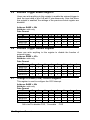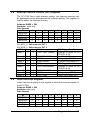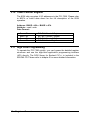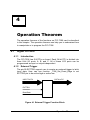
1
NuDAQ PCI-7396 DIN-96DI, DIN-96DO 96-CH Digital I/O Cards User’s Guide @Copyright 2000 ADLINK Technology Inc. All Rights Reserved. Manual Rev. 1.12: September 4, 2000 The information in this document is subject to change without prior notice in order to improve reliability, design and function and does not represent a commitment on the part of the manufacturer. In no event will the manufacturer be liable for direct, indirect, special, incidental, or consequential damages arising out of the use or inability to use the product or documentation, even if advised of the possibility of such damages. This document contains proprietary information protected by copyright. All rights are reserved. No part of this manual may be reproduced by any mechanical, electronic, or other means in any form without prior written permission of the manufacturer. Trademarks NuDAQ, DAQBench Technology Inc. are registered trademarks of ADLINK Other product names mentioned herein are used for identification purposes only and may be trademarks and/or registered trademarks of their respective companies. Getting service from ADLINK ♦ Customer Satisfaction is always the most important thing for ADLINK Tech Inc. If you need any help or service, please contact us and get it. ADLINK Technology Inc. Web Site Sales & Service Technical Support TEL Address ♦ http://www.adlink.com.tw http://www.adlinktechnology.com [email protected] NuDAQ [email protected] NuDAM [email protected] NuIPC [email protected] NuPRO [email protected] Software [email protected] +886-2-82265877 FAX +886-2-82265717 9F, No. 166, Jian Yi Road, Chungho City, Taipei, 235 Taiwan, R.O.C. Please inform or FAX us of your detailed information for a prompt, satisfactory and constant service. Detailed Company Information Company/Organization Contact Person E-mail Address Address Country TEL Web Site FAX Questions Product Model Environment to Use Challenge Description Suggestions for ADLINK ¨OS: ¨Computer Brand: ¨M/B: ¨CPU: ¨Chipset: ¨Bios: ¨Video Card: ¨Network Interface Card: ¨Other: CONTENTS How to Use This Guide ................................................ iv Chapter 1 Introduction ................................................1 1.1 Features................................................................................. 1 1.1.1 1.1.2 1.1.3 1.2 1.3 1.4 Digital I/O Ports....................................................................1 Timer / Counter and Interrupt System.................................1 Miscellaneous ......................................................................2 Applications .......................................................................... 2 Specifications ....................................................................... 2 Software Supporting ............................................................ 3 1.4.1 1.4.2 1.4.3 1.4.4 1.4.5 1.4.6 1.4.7 1.4.8 Programming Library...........................................................3 ® PCIS-LVIEW: LabVIEW Driver............................................4 PCIS-VEE: HP-VEE Driver....................................................4 DAQBenchTM: ActiveX Controls ..........................................4 PCIS-DDE: DDE Server and InTouchTM...............................4 PCIS-ISG: ISaGRAFTM driver................................................4 PCIS-ICL: InControlTM Driver ...............................................4 PCIS-OPC: OPC Server .......................................................5 Chapter 2 Installation ..................................................6 2.1 2.2 2.3 2.4 2.5 2.6 2.7 What You Have...................................................................... 6 Unpacking ............................................................................. 7 PCI-7396 Layout.................................................................... 8 Hardware Installation Outline .............................................. 9 Device Installation for Windows Systems ........................... 9 Connectors’ Pin Assignment ............................................. 10 Jumpers’ Description ......................................................... 11 2.7.1 2.8 Power-on-state...................................................................11 Termination Boards Supporting ........................................ 12 2.8.1 2.8.2 2.8.3 Connect with DIN-100S......................................................12 Connect with DIN-96DI.......................................................12 Connect with DIN-96DO.....................................................12 Chapter 3 Registers Format ......................................13 3.1 3.2 PCI PnP Registers............................................................... 13 I/O Address Map ................................................................. 14 Contents • i 3.3 3.4 3.5 3.6 3.7 3.8 3.9 3.10 3.11 Digital Data Registers ......................................................... 15 Control Register................................................................. 15 External Trigger Enable Register....................................... 16 External Trigger Disable Register...................................... 16 Change of State (COS) Control Register ........................... 16 Interrupt Source Control (ISC) Register ............................ 17 Clear Interrupt Register ...................................................... 17 Timer/Counter Register ...................................................... 18 High Level Programming.................................................... 18 Chapter 4 Operation Theorem...................................19 4.1 Digital I/O Ports................................................................... 19 4.1.1 4.1.2 4.2 8254 Timer/Counter Operation........................................... 20 4.2.1 4.2.2 4.2.3 4.3 Introduction........................................................................20 Cascaded 32 bits Timer .....................................................21 Event Counter and Edge Control.......................................21 Interrupt Circuit................................................................... 21 4.3.1 4.3.2 4.3.3 4.3.4 4.3.5 4.4 Introduction........................................................................19 External Trigger .................................................................19 System Architecture ..........................................................21 IRQ Level Setting ...............................................................21 Dual Interrupt System........................................................21 Interrupt Source Control (ISC)...........................................22 Change of State (COS) Interrupt .......................................23 12V and 5V Power Supply .................................................. 24 Chapter 5 C/C++ Libraries .........................................25 5.1 5.2 Libraries Installation.......................................................... 25 Programming Guide ........................................................... 26 5.2.1 5.2.2 5.3 5.4 5.5 5.6 5.7 5.8 5.9 5.10 5.11 Naming Convention ...........................................................26 Data Types .........................................................................26 _7396_Initial ........................................................................ 27 _7396_DI .............................................................................. 27 _7396_DO ............................................................................ 28 _7396_Config_Port ............................................................. 29 _7396_Software_Reset ....................................................... 31 _7396_INT_Source_Control................................................ 31 _7396_COSIRQ_Control ..................................................... 32 _7396_CLR_IRQ .................................................................. 32 _7396_Set_Event_Edge ...................................................... 33 ii • Contents 5.12 _7396_Cascaded_Timer...................................................... 33 5.13 _7396_Timer_Start .............................................................. 34 5.14 _7396_Timer_Read.............................................................. 34 Appendix A1 DIN-96DI ...............................................36 A1.1 A1.2 A1.3 A1.4 A1.5 Introductions....................................................................... 36 Features............................................................................... 36 Specifications ..................................................................... 36 Layout of DIN-96DI.............................................................. 37 DI Circuits and Wiring ........................................................ 38 Appendix A2 DIN-96DO ..............................................39 A2.1 A2.2 A2.3 A2.4 A2.5 Introductions....................................................................... 39 Features............................................................................... 39 Specifications ..................................................................... 39 Layout of DIN-96DO ............................................................ 40 Circuits and Wiring............................................................. 41 Product Warranty/Service...........................................43 Contents • iii How to Use This Guide This manual is designed to help you use the PCI-7396. It describes how to modify and control various functions on the PCI-7396 card to meet your requirements. It is divided into three chapters: • Chapter 1, "Introduction," gives an overview of the product features. applications, and specifications. • Chapter 2, "Installation," describes how to install the PCI-7396. The layout of PCI-7396 is shown. The jumper settings, the connectors’pin assignment, and the other notes for installation are described. • Chapter 3, "Registers’ Format," describes the details of registers’ format and structure of the PCI-7396, this information is very important for the programmers who want to control the hardware by low-level programming language. • Chapter 4, "Operation Theorem" describes more details about the versatile functions, including DIO, timer / counter, and interrupt systems. • Chapter 5, "C/C++ Software Libraries" specifies the software libraries of C/C++ language under DOS environment that make you operate the functions of this card easily. iv • Contents 1 Introduction The PCI-7396 is a 48/96-bit parallel digital input/output (DIO) card designed for industrial applications. The plug and play feature of PCIBus architecture make it easy for users to install their systems quickly. The PCI-7396 emulates two/four 8255 Programmable Peripheral Interface (PPI) chips. Each PPI offers 3 8-bit DIO ports which can be accessed simultaneously. The total 6/12 ports can be programmed as input or output independently. The PCI-7396 supports external trigger to latch the digital input data. The function of “Change of State” (COS) interrupt is provided. It means when anyone of these digital inputs changes its state, an interrupt will be generated for user to handle this external event. 1.1 Features The PCI-7396 Digital I/O boards provide the following advanced features: 1.1.1 Digital I/O Ports • 48/96 TTL compatible digital I/O lines • SCSI-type 100-pin connector (AMP-787082-9) • 48mA High current driving capability per channel • Output status read-back • Support external trigger to latch digital input data (PCI-7348 only) 1.1.2 • • • • Timer / Counter and Interrupt System A programmable 32-bit timer to generate timer interrupt A programmable 16-bit event counter to generate event interrupt 48/96-bit change of state (COS) interrupt Dual interrupt system Introduction • 1 1.1.3 Miscellaneous • Provide 12V and 5V power supply on SCSI-type 100-pin connectors(only for PCI-7348) • On board resettable fuses to protect power supply from external damage. (only for PCI-7348) 1.2 Applications • • • • • 1.3 Programmable mixed digital input & output Industrial monitoring and controlling LED indicator driving Parallel data transfer TTL,DTL, and CMOS logic sensing Specifications Output Signal 48-bit for PCI-7348 96-bit for PCI-7396 Logic High Voltage Logic Low Voltage Logic High Current Logic Low Current Logic High Voltage Operating Temperature Storage Temperature Humidity I/O Connectors Bus IRQ Level I/O port address Power Consumption (without external devices) Transfer Rate Size Logic Low Voltage Logic High Current Logic Low Current 0° ~ 60° C -20° ~ 80° C 5% ~ 95% non-condensing 100-pin SCSI connector PCI bus, rev 2.1 Set by PCI BIOS Set by PCI BIOS PCI-7348 : 350mA (TYP) PCI-7396 : 450mA (TYP) 1M bytes/sec (Typical) Half-size PCB : 158 mm x 107 mm I/O channels Input Signal 2 • Introduction : 2.0 V to 5.25V : 0.0 V to 0.80V : 0.1 uA : -8 mA : Typical 3.3 V : Minimum 2.4 V : Maximum 0.5V : -15.0 mA : 48.0 mA 1.4 Software Supporting ADLink provides versatile software drivers and packages for users’ different approach to built-up a system. We not only provide programming library such as DLL for many Windows systems, but ® also provide drivers for many software package such as LabVIEW , TM TM TM TM TM HP VEE , DASYLab , InTouch , InControl , ISaGRAF , and so on. All the software options are included in the ADLink CD. The non-free software drivers are protected with serial licensed code. Without the software serial number, you can still install them and run the demo version for two hours for demonstration purpose. Please contact with your dealer to purchase the formal license serial code. 1.4.1 Programming Library For customers who are writing their own programs, we provide function libraries for many different operating systems, including: u DOS Library: Borland C/C++ and Microsoft C++, the functions descriptions are included in this user’s guide. u Windows 95 DLL: For VB, VC++, Delphi, BC5, the functions descriptions are included in this user’s guide. u PCIS-DASK: Include device drivers and DLL for Windows 98, Windows NT and Windows 2000. DLL is binary compatible across Windows 98, Windows NT and Windows 2000. That means all applications developed with PCIS-DASK are compatible across Windows 98, Windows NT and Windows 2000. The developing environment can be VB, VC++, Delphi, BC5, or any Windows programming language that allows calls to a DLL. The user’s guide and function reference manual of PCIS-DASK are in the CD. Please refer the PDF manual files under (\\Manual_PDF\Software\PCIS-DASK) u PCIS-DASK/X: Include device drivers and shared library for Linux. The developing environment can be Gnu C/C++ or any programming language that allows linking to a shared library. The user's guide and function reference manual of PCISDASK/X are in the CD. (\\Manual_PDF\Software\PCIS-DASK-X.) The above software drivers are shipped with the board. Please refer to the “Software Installation Guide” to install these drivers. Introduction • 3 ® 1.4.2 PCIS-LVIEW: LabVIEW Driver PCIS-LVIEW contains the VIs, which are used to interface with NI’s ® LabVIEW software package. The PCIS-LVIEW supports Windows ® 95/98/NT/2000. The LabVIEW drivers are free shipped with the board. You can install and use them without license. For detail information about PCIS-LVIEW, please refer to the user’s guide in the CD. (\\Manual_PDF\Software\PCIS-LVIEW) 1.4.3 PCIS-VEE: HP-VEE Driver The PCIS-VEE includes the user objects, which are used to interface with HP VEE software package. PCIS-VEE supports Windows 95/98/NT. The HP-VEE drivers are free shipped with the board. You can install and use them without license. For detail information about PCIS-VEE, please refer to the user’s guide in the CD. (\\Manual_PDF\Software\PCIS-VEE) 1.4.4 DAQBenchTM: ActiveX Controls We suggest the customers who are familiar with ActiveX controls and VB/VC++ programming use the DAQBenchTM ActiveX Control components library for developing applications. The DAQBenchTM is designed under Windows NT/98. For more detailed information about DAQBench, please refer to the user’s guide i n the CD. (\\Manual_PDF\Software\DAQBench\DAQBench Manual.PDF) 1.4.5 PCIS-DDE: DDE Server and InTouchTM DDE stands for Dynamic Data Exchange specifications. The PCISDDE includes the PCI cards’ DDE server. The PCIS -DDE server is included in the ADLINK CD. It needs license. The DDE server can be used conjunction with any DDE client under Windows NT. 1.4.6 PCIS-ISG: ISaGRAFTM driver The ISaGRAF WorkBench is an IEC1131-3 SoftPLC control program development environment. The PCIS-ISG includes ADLink products’ target drivers for ISaGRAF under Windows NT environment. The PCIS-ISG is included in the ADLINK CD. It needs license. 1.4.7 PCIS-ICL: InControlTM Driver 4 • Introduction PCIS-ICL is the InControl driver which support the Windows NT. The PCIS-ICL is included in the ADLINK CD. It needs license. 1.4.8 PCIS-OPC: OPC Server PCIS-OPC is an OPC Server, which can link with the OPC clients. There are many software packages on the market can provide the OPC clients now. The PCIS-OPC supports the Windows NT. It needs license. Introduction • 5 2 Installation This chapter describes how to install the PCI-7396. The contents in the package and unpacking information that you should be careful are described. Please follow the steps to install the PCI-7348/7396. w w w w w 2.1 Check what you have (section 2.1) Unpacking (section 2.2) Check the PCB (section 2.3) Install the hardware (section 2.4) Please refer to the “Software Installation Guide” to install the software drivers. What You Have In addition to this User's Manual, the package includes the following items: • PCI-7396 96-bits Parallel Digital I/O Card • ADLINK CD • Software Installation Guide If any of thes e items is missing or damaged, contact the dealer from whom you purchased the product. Save the shipping materials and carton in case you want to ship or store the product in the future. 6 • Installation 2.2 Unpacking Your PCI-7396 card contains sensitive electronic components that can be easily damaged by static electricity. The card should be done on a grounded anti-static mat. The operator should be wearing an anti-static wristband, grounded at the same point as the anti-static mat. Inspect the card module carton for obvious damage. Shipping and handling may cause damage to your module. Be sure there are no shipping and handing damages on the module before processing. After opening the card module carton, exact the system module and place it only on a grounded anti-static surface component side up. Note: DO NOT APPLY POWER TO THE CARD IF IT HAS BEEN DAMAGED. You are now ready to install your PCI-7396. Installation • 7 2.3 PCI-7396 Layout Figure 2.1 PCI-7396 Layout 8 • Installation 2.4 Hardware Installation Outline Hardware configuration The PCI cards (or CompactPCI cards) are equipped with plug and play PCI controller, it can request base addresses and interrupt according to PCI standard. The system BIOS will install the system resource based on the PCI cards’ configuration registers and system parameters (which are set by system BIOS). Interrupt assignment and memory usage (I/O port locations) of the PCI cards can be assigned by system BIOS only. These system resource assignments are done on a boardby-board basis. It is not suggested to assign the system resource by any other methods. PCI slot selection The PCI card can be inserted to any PCI slot without any configuration for system resource. Installation Procedures 1. Turn off your computer 2. Turn off all accessories (printer, modem, monitor, etc.) connected to your computer. 3. Remove the cover from your computer. 4. Setup jumpers on the PCI or CompactPCI card. 5. Select a 32-bit PCI slot. PCI slot are short than ISA or EISA slots, and are usually white or ivory. 6. Before handling the PCI cards, discharge any static buildup on your body by touching the metal case of the computer. Hold the edge and do not touch the components. 7. Position the board into the PCI slot you selected. 8. Secure the card in place at the rear panel of the system. 2.5 Device Installation for Windows Systems Once Windows 95/98/2000 has started, the Plug and Play function of Windows system will find the new NuDAQ/NuIPC cards. If this is the first time to install NuDAQ/NuIPC cards in your Windows system, you will be informed to input the device information source. Please refer to the “Software Installation Guide” for the steps of installing the device. Installation • 9 2.6 (1) (2) (3) (48) (49) (50) Connectors’ Pin Assignment (51) (52) (53) (98) (99) (100) (1) P1A0 (2) P1A1 (3) P1A2 (4) P1A3 (5) P1A4 (6) P1A5 (7) P1A6 (8) P1A7 (9) P1B0 (10) P1B1 (11) P1B2 (12) P1B3 (13) P1B4 (14) P1B5 (15) P1B6 (16) P1B7 (17) P1C0 (18) P1C1 (19) P1C2 (20) P1C3 (21) P1C4 (22) P1C5 (23) P1C6 (24) P1C7 (25) GND (26) P2A0 (27) P2A1 (28) P2A2 (29) P2A3 (30) P2A4 (31) P2A5 (32) P2A6 (33) P2A7 (34) P2B0 (35) P2B1 (36) P2B2 (37) P2B3 (38) P2B4 (39) P2B5 (40) P2B6 (41) P2B7 (42) P2C0 (43) P2C1 (44) P2C2 (45) P2C3 (46) P2C4 (47) P2C5 (48) P2C6 (49) P2C7 (50) GND (51) P3A0/EVENT (76) (52) P3A1 (77) (53) P3A2 (78) (54) P3A3 (79) (55) P3A4 (80) (56) P3A5 (81) (57) P3A6 (82) (58) P3A7 (83) (59) P3B0 (84) (60) P3B1 (85) (61) P3B2 (86) (62) P3B3 (87) (63) P3B4 (88) (64) P3B5 (89) (65) P3B6 (90) (66) P3B7 (91) (67) P3C0 (92) (68) P3C1 (93) (69) P3C2 (94) (70) P3C3 (95) (71) P3C4 (96) (72) P3C5 (97) (73) P3C6 (98) (74) P3C7 (99) (75) GND (100) P4A0 P4A1 P4A2 P4A3 P4A4 P4A5 P4A6 P4A7 P4B0 P4B1 P4B2 P4B3 P4B4 P4B5 P4B6 P4B7 P4C0 P4C1 P4C2 P4C3 P4C4 P4C5 P4C6 P4C7/EXTTRG GND Figure 2.3 Connectors Pin Assignment of PCI-7396 The DIO pin names are specified as PnXb, where n : means the PPI number of the PCI-7396, n=1~4 X : means the port name of the PPI, X= A ‘ ’, B ‘ ’or C ‘ ’ b : means the bit number of the port, b=0~7 For example, P1C4 means bit 4 of port C on PPI1. EXTTRG : External trigger signal to latch digital input data EVENT : External event source for counter 0 GND : Ground 10 • Installation 2.7 Jumpers’ Description The PCI-7396 is a p‘ lug and play’add -on card using PCI bus. It is unnecessary for user to setup its base address and IRQ level to fit the hardware of your computer system. However, to fit users’ versatile operation, there are still a few jumpers to set the power-on-states of all I/O ports. 2.7.1 Power-on-state For all I/O ports of the PCI-7396, the power-on-states could be pulled high, pulled low, or floating. It is depended on the jumper settings. Table 2.1 lists the reference numbers of jumpers and their corresponding port names. Jumper JA1 JB1 JC1 JA2 JB2 JC2 Port Name P1A P1B P1C P2A P2B P2C Jumper JA3 JB3 JC3 JA4 JB4 JC4 Port Name P3A P3B P3C P4A P4B P4C Table 2.1 Jumpers and port names list All the jumpers are identical physically. The power-on-state of each port can be set independently. To pull all signals low is the default settings. The following diagram use JA1 as an example to show the possible settings. JA1 Port A of PPI1 is pulled low.(default setting) JA1 Port A of PPI1 is pulled high. When the jumper cap is removed, the power-on-state is floating. Installation • 11 2.8 Termination Boards Supporting PCI-7396 can be connected with several different daughter boards, including DIN-100S, DIN-96DI, and DIN-96DO. The functionality and connections are specified as follows. 2.8.1 Connect with DIN-100S DIN-100S is a direct connector for the add-on card that is equipped with SCSI-100 connector. It is suitable for the simple applications that do not need isolated connection in front of the digital inputs or outputs of PCI-7396. 2.8.2 Connect with DIN-96DI DIN-96DI digital input termination board features high-voltage optoisolation on all inputs to prevent floating potential and ground loop problems from damaging your PC system. It is composed of one TB96 base board, one TB-96DI daughter board, and one DIN socket for easy maintenance, wiring, and installation. It provides 96 channels that are accessed through a SCSI-100 connector.(see Appendix A1) 2.8.3 Connect with DIN-96DO DIN-96DO digital output termination board features high-voltage optoisolation on all outputs to prevent floating potential and ground loop problems from damaging your PC system. It is composed of one TB96 base board, one TB-96DO daughter board, and one DIN socket for easy maintenance, wiring, and installation. It provides 96 channels that are accessed through a SCSI-100 connector. (see Appendix A2) 12 • Installation 3 Registers Format The detailed descriptions of the registers format are specified in this chapter. This information is quite useful for the programmers who wish to handle the card by low-level programming. However, we suggest user have to understand more about the PCI interface then start any low-level programming. In addition, the contents of this chapter can help users understand how to use software driver to manipulate this card. 3.1 PCI PnP Registers This PCI card functions as a 32-bit PCI target device to any master on the PCI bus. There are three types of registers: PCI Configuration Registers (PCR), Local Configuration Registers (LCR) and PCI-6308 registers. The PCR, which is compliant to the PCI-bus specifications, is initialized and controlled by the plug & play (PnP) PCI BIOS. User‘s can study the PCI BIOS specification to understand the operation of the PCR. Please contact with PCISIG to acquire the specifications of the PCI interface. The PCI bus controller PCI-9050 is provided by PLX technology Inc. (www.plxtech.com). For more detailed information of LCR, please visit PLX technology’s web site to download relative information. It is not necessary for users to understand the details of the LCR if you use the software library. The PCI PnP BIOS assigns the base address of the LCR. The assigned address is located at offset 14h of PCR. The PCI-6308 registers are shown in the next section. The base address, which is also assigned by the PCI PnP BIOS, is located at offset 18h of PCR. Therefore, users can read the 18h of PCR to know the base address by using the BIOS function call. Registers Format • 13 Please do not try to modify the base address and interrupt which assigned by the PCI PnP BIOS, it may cause resource confliction in your system. 3.2 I/O Address Map Most of the PCI-7396 registers are 32 bits. The users can access these registers by 32 bits I/O instructions. The following table shows the registers map, including descriptions and their offset addresses relative to the base address. Offset 0x00 0x04 0x08 0x0C 0x10 0x14 0x18 0x1C 0x20 0x24 0x28 0x2C 0x30 0x34 0x38 0x3C 0x40 0x44 0x48 0x4C 0x50 0x54 0x60 0x64 0x68 0x6C Write P1ABC P1Control P1EXTTRG Enable P1EXTTRG Disable P2ABC P2Control P2EXTTRG Enable P2EXTTRG Disable P3ABC P3Control P3EXTTRG Enable P3EXTTRG Disable P4ABC P4Control P4EXTTRG Enable P4EXTTRG Disable Timer/Counter #0 Timer/Counter #1 Timer/Counter #2 Timer/Counter Mode Control ISC: Interrupt Source Control Clear Interrupt P1 COS Control P2 COS Control P3 COS Control P4 COS Control Read P1ABC No used No used No used P2ABC No used No used No used P3ABC No used No used No used P4ABC No used No used No used Timer/Counter #0 Timer/Counter #1 Timer/Counter #2 Timer/Counter Mode Status No used No used No used No used No used No used Table 3.1 Register Map The PCI-7396 has 2/4 PPIs on board. Each PPI contains 5 registers, including Digital Data Register, Control Register, External Trigger 14 • Registers Format Enable Register, External Trigger Disable Register, and COS Interrupt Control Register. In the following sections, the 5 registers of PPI1 will be introduced respectively. The registers of the other 3 PPIs are of the same configuration which will not be repeated in this manual. 3.3 Digital Data Registers The 24-bit I/O data of the PCI-7396 is accessed from/to this register by software. The digital data can also be read back through this register. Address: BASE + 00h Attribute: read and write Data Format: Bit BASE+ 00h BASE+ 01h BASE+ 02h BASE+ 03h 7 P1A7 P1B7 P1C7 X 6 P1A6 P1B6 P1C6 X 5 P1A5 P1B5 P1C5 X 4 3 P1A4 P1A3 P1B4 P1B3 P1C4 P1C3 X X 2 P1A2 P1B2 P1C2 X 1 P1A1 P1B1 P1C1 X 0 P1A0 P1B0 P1C0 X P1X7~P1X0: Digital I/O data X:A~C. 3.4 Control Register Each PPI’s control register is used to set its three ports to be as input or output one independently. Address: BASE + 04h Attribute: write only Data Format: Bit BASE+ 04h BASE+ 05h BASE+ 06h BASE+ 07h 7 x x x x 6 x x x x 5 x x x x 4 x x x x 3 x x x x 2 P1C x x x 1 P1B x x x 0 P1A x x x P1n : n: port number Set to be 0‘ ’for input port , 1‘ ’ for output port Registers Format • 15 3.5 External Trigger Enable Register Users can write anything to this register to enable the external trigger to latch the input data of port A,B and C simultaneously. Note that when this register is enabled, the settings of the previous control register are disabled. Address: BASE + 08h Attribute: write only Data Format: Bit BASE+08h BASE+09h BASE+0Ah BASE+0Bh 3.6 7 x x x x 6 x x x x 5 x x x x 4 x x x x 3 x x x x 2 x x x x 1 x x x x 0 x x x x External Trigger Disable Register Users can write anything to this register to disable the function of external trigger. Address: BASE + 0Ch Attribute: write only Data Format: Bit BASE+0Ch BASE+0Dh BASE+0Eh BASE+0Fh 3.7 7 x x x x 6 x x x x 5 x x x x 4 x x x x 3 x x x x 2 x x x x 1 x x x x 0 x x x x 1 P1B x x x 0 P1A x x x Change of State (COS) Control Register This register is used to configure the COS interrupt. Address: BASE + 60h Attribute: write only Data Format: Bit 7 6 5 4 3 2 BASE+60h x x x x x P1C BASE+61h x x x x x x BASE+62h x x x x x x BASE+64h x x x x x x P1n : n: port number Set to be 0‘ ’to disable COS , 1‘ ’to enable COS 16 • Registers Format 3.8 Interrupt Source Control (ISC) Register The PCI-7396 has a dual interrupt system, two interrupt sources can be generated and be distinguished by software setting. This register is used to select the interrupt sources. Address: BASE + 50h Attribute: write only Data Format: Bit 7 BASE+50h x BASE+51h x BASE+52h x BASE+54h x 6 x x x x 5 x x x x 4 x x x x 3 C2_1 x x x C1_0,C1_1 : Select source INT 1 C2_0,C2_1 : Select source INT 2 C1_1 C1_0 IRQ Sources INT1 Mode 1 0 0 COS P1&P2 (48bits) Mode 2 Mode 3 Mode 4 INT2 Mode 1 3.9 1 0 1 0 1 1 1 0 1 1 C1_1 x x x 0 C1_0 x x x IRQ Trigger Condition Change of State for PCI7396 P1 & P2 (see Table 4.2) falling edge of P1C0 Counter count down to 0 IRQ Trigger Condition Change of State for PCI7396 P3 & P4 (see Table 4.2) falling edge of P2C0 Timer count down to 0 P1C0 OR ~P1C3 ~P1C0 Event Counter C2_1 C2_0 IRQ Sources 0 0 COS P3&P4(48bits) Mode 2 Mode 3 Mode 4 0 1 1 2 C2_0 x x x P2C0 OR ~P2C3 ~P2C0 32-bit Timer Clear Interrupt Register Users can write anything to this register to clear the interrupt request of the PCI-7396. Address: BASE + 54h Attribute: write only Data Format: Bit BASE+54h BASE+55h BASE+56h BASE+57h 7 x x x x 6 x x x x 5 x x x x 4 x x x x 3 x x x x 2 x x x x 1 x x x x 0 x x x x Registers Format • 17 3.10 Timer/Counter Register The 8254 chip occupies 4 I/O addresses in the PCI-7396. Please refer to NEC's or Intel's data sheet for the full description of the 8254 operation. Address : BASE + 40h ~ BASE + 4Ch Attribute : read / write Data Format : Base + 40h Base + 44h Base + 48h Base + 4Ch Bit 7~Bit 0: Counter 0 Register Bit 7~Bit 0: Counter 1 Register Bit 7~Bit 0: Counter 2 Register Bit 7~Bit 0: Control Register 3.11 High Level Programming To operate the PCI-7396 quickly, you can bypass the detailed register structures and use the high-level application programming interface (API) directly. The DOS library for Borland C/C++ is included in the ADLINK CD. Please refer to chapter 5 for more detailed information. 18 • Registers Format 4 Operation Theorem The operation theorem of the functions on PCI-7396 card is described in this chapter. The operation theorem can help you to understand how to manipulate or to program the PCI-7396. 4.1 Digital I/O Ports 4.1.1 Introduction The PCI-7396 has 2/4 PPIs on board. Each 24-bit PPI is divided into three 8-bit I/O ports: A, B, and C. All of these 6/12 ports can be programmed as input or output independent. 4.1.2 External Trigger The pin-99 EXTTRG support user to receive an external trigger to latch input data. User can use function _7396_Set_Event_Edge to set EXTTRG pin to be active high or active low. INPUT DATA DATA to PC EXTTRG Read Data Figure 4.1 External Trigger Function Block Operation Theorem • 19 EXTTRG Latch Data (Latch input data to registers) Read Data (Read date from registers to PC) Figure 4.2 Read Data use External Trigger 4.2 8254 Timer/Counter Operation 4.2.1 Introduction One 8254 programmable timer/counter chip is installed in the PCI7396. There are three counters in one 8254 chip and 6 possible operation modes for each counter. The block diagram of the timer /counter system is shown in Figure 4.3. EVENT (PIN 51) 8254 Chip Event Edge Control Counter #0 Event IRQ Gate='H' Timer #1 2 MHz Clock Gate='H' Timer #2 Timer IRQ Gate='H' Figure 4.3 Timer / counter system of PCI-7396. Timer #1 and timer #2 of the 8254 chip are cascaded as a 32-bits programmable timer. In the software library, timer #1 and #2 are always set as mode 2 (rate generator). Counter #0 is used as an event counter, that is, there is an interrupt on the terminal count of 8254 mode 0. 20 • Operation Theorem 4.2.2 Cascaded 32 bits Timer The base frequency of input clock for the cascaded timer is 2MHz. The output is send to be the timer interrupt. To set the maximum and minimum frequency of the timer, please refer to the function _7348_Cascaded_Timer or _7396_Cascaded_Timer. 4.2.3 Event Counter and Edge Control The counter #0 of 8254 is used to be an event counter. The input is pin-51 of CN1. The trigger edge of counter clock is programmable. The gate control fixs high (enable). The output is send to be the event interrupt. That means If counter #0 is set as 8254 mode 0, the event IRQ asserts as the counter counts down to zero. 4.3 Interrupt Circuit 4.3.1 System Architecture The PCI-7396‘s interrupt system is powerful and flexible, which is suitable for many applications. It is a Dual Interrupt System. The dual interrupt means the hardware can generate two interrupt request signals in the same time and the software can service these two request signals by ISR. Note that the dual interrupt do not mean the card occupy two IRQ levels. The two interrupt request signals (INT1 and INT2) comes from digital inputs or the timer/counter outputs. Two multiplexers (MUX) are used to select the IRQ sources. Fig 4.4 shows the interrupt system. 4.3.2 IRQ Level Setting There is only one IRQ level needed in the PCI-7396, although it is a dual interrupt system. This card uses INT #A interrupt request signal on PCI bus. The mother board circuits will transfer INT #A to one of the AT bus IRQ levels. The IRQ level is set by the PCI plug and play BIOS and saved in the PCI controller. It is not necessary for users to set the IRQ level. Users can get the IRQ level by software library. 4.3.3 Dual Interrupt System The PCI controller can receive two hardware IRQ requests. However, only one IRQ will be sent to PCI bus, the two IRQ requests must be distinguished by user’s interrupt service routine (ISR). The two IRQ requests are named as INT1 and INT2. INT1 comes from COS P1 & P2, P1C0, P1C3, or the event counter interrupt. INT2 comes from COS P3 & P4, P2C0, P2C3, or the timer interrupt. The Operation Theorem • 21 sources of INT1 and INT2 is selectable by using the Interrupt Source Control (ISC) Register. INT1 INT #A PCI Controller INT2 INT1 MUX ~P1C0 P1C0/~P1C3 COS P1 & P2 Event IRQ INT2 MUX ~P2C0 P2C0/~P2C3 COS P3 & P4 Timer IRQ IRQ FlipFlops Clear IRQ Figure 4.4 Dual Interrupt System of PCI-7396 4.3.4 Interrupt Source Control (ISC) There are four bits to control the IRQ sources of INT1 and INT2. Table 4.1 shows the selection of the IRQ sources and the interrupt trigger condition. If the application needs one IRQ only, you can disable one of the IRQ sources by software. You can also disable both the two interrupts If you do not need any IRQ source. However, the PCI BIOS still assign a IRQ level to the PCI card and occupy the PC resource if you only disable the IRQ sources without change the initial condition of the PCI controller. IRQ Trigger Condition INT1 C1 C2 IRQ Sources Disable 4 X INT1 disable -Mode 1 0 X COS P1&P2 (48bits) Change of State for PCI-7396 Mode 2 1 X P1C0 OR ~P1C3 (see following) Mode 3 2 X ~P1C0 falling edge of P1C0 Mode 4 3 X Event Counter Counter count down to 0 INT2 C1 C2 IRQ Sources IRQ Trigger Condition Disable X 4 INT2 disable -Mode 1 X 0 COS P3&P4 (48bits) Change of State for PCI-7396 Mode 2 X 1 P2C0 OR ~P2C3 (see following) Mode 3 X 2 ~P2C0 falling edge of P2C0 Mode 4 X 3 Timer Output Timer count down to 0 Table 4.1 ISC register format Default settings 22 • Operation Theorem When the IRQ sources is set as “P1C0 OR ~P1C3” or “P2C0 OR ~P2C3”, the IRQ trigger conditions are summarized in Table 4.2, P1C0 High X Low 0->1 P2C0 High X Low 0->1 P1C3 X Low 1->0 High P2C3 X Low 1->0 High IRQ Trigger Condition P1C0=‘H’disable all IRQ P1C3=‘L’disable all IRQ P1C3 falling edge trigger when P1C0=L P1C0 rising edge trigger when P1C3=H IRQ Trigger Condition P2C0=‘H’disable all I RQ P2C3=‘L’disable all IRQ P2C3 falling edge trigger when P2C0=L P2C0 rising edge trigger when P2C3=H Table 4.2 IRQ Trigger conditions By using the four signals: P1C0, P2C0, P1C3, and P2C3, user can utilize their combination to generate a proper IRQ for versatile applications. 4.3.5 Change of State (COS) Interrupt What is COS? The COS (Change of State) means when the input state (logic level) is changed from low to high, or from high to low. The COS detection circuit will detect the edge of level change. In the PCI-7396 card, the COS detection circuit is applied to all the input channels. When any channel changes its logic level, the COS detection circuit generates an interrupt request to PCI controller. P1A0 P2A0 COS 1 COS2 INT1 Clear_IRQ Clear_IRQ Clear_IRQ Operation Theorem • 23 COS Detection The following timing is an example of COS operation. All the DI signals’ level change will be detected and then take an O ‘ R’ operation to generate the INT1 or INT2 IRQ request. If INT1 or INT2 IRQ request generates, the signal will be latched. User should apply the function “_7396_CLR_IRQ” or “_7348_CLR_IRQ” to reset its state, after the corresponding ISR is finished,. 4.4 12V and 5V Power Supply The SCSI-100 connector CN1 provides +12V and +5V power supply (only for PCI-7348) for external devices. To avoid the short circuit or the overload of the power supply, the resettable fuses are added on all the power supply signals. The maximum current for 5V power supply is 0.5 A. If the load current is larger than this limitation, the resistance of the resettable fuse will increase for the reason of the rising temperature. The rising resistance will further cause the power supply to reduce the load current. After the condition of overload or short circuit is removed, the fuse will return to its normal condition. It is unnecessary to replace the fuse. The maximum current of 12V power supply is 0.5A, too. The action of the fuse is the same as that of +5V power supply. 24 • Operation Theorem 5 C/C++ Libraries This chapter describes the software library for operating this card. Only the functions in DOS library and Windows 95 DLL are described. Please refer to the PCIS-DASK function reference manual, which included in ADLINK CD, for the descriptions of the Windows 98/NT/2000 DLL functions. The function prototypes and some useful constants are defined in the header files LIB directory (DOS) and INCLUDE directory (Windows 95). For Windows 95 DLL, the developing environment can be Visual Basic 4.0 or above, Visual C/C++ 4.0 or above, Borland C++ 5.0 or above, Borland Delphi 2.x (32-bit) or above, or any Windows programming language that allows calls to a DLL. It provides the C/C++, VB, and Delphi include files. 5.1 Libraries Installation Please refer to the “Software Installation Guide” for the detail information about how to install the software libraries for DOS, or Windows 95 DLL, or PCIS-DASK for Windows 98/NT/2000. The device drivers and DLL functions of Windows 98/NT/2000 are included in the PCIS-DASK. Please refer the PCIS-DASK user’s guide and function reference, which included in the ADLINK CD, for detailed programming information. C/C++ Libraries • 25 5.2 Programming Guide 5.2.1 Naming Convention The functions of the NuDAQ PCI cards or NuIPC CompactPCI cards’ software driver are using full-names to represent the functions' real meaning. The naming convention rules are: In DOS Environment : _{hardware_model}_{action_name}. e.g. _7396_Initial(). In order to recognize the difference between DOS library and Windows 95 library, a capital "W" is put on the head of each function name of the Windows 95 DLL driver. e.g. W_7396_Initial(). 5.2.2 Data Types We defined some data type in Pci_7396.h (DOS) and Acl_pci.h (Windows 95). These data types are used by NuDAQ Cards’ library. We suggest you to use these data types in your application programs. The following table shows the data type names and their range. Type Name U8 I16 U16 I32 U32 F32 F64 Boolean 26 • C/C++ Libraries Description Range 8-bit ASCII character 0 to 255 16-bit signed integer -32768 to 32767 16-bit unsigned integer 0 to 65535 32-bit signed integer -2147483648 to 2147483647 32-bit single-precision 0 to 4294967295 floating-point 32-bit single-precision -3.402823E38 to 3.402823E38 floating-point 64-bit double-precision floating-point Boolean logic value -1.797683134862315E308 to 1.797683134862315E309 TRUE, FALSE 5.3 _7396_Initial @ Description This function is used to initialize the PCI-7396. Every PCI-7396 has to be initialized by this function before calling other functions. @ Syntax C/C++ (DOS) U16 _7396_Initial (U16 *existCards, PCI_INFO *pciInfo) C/C++ (Windows 95) U16 W_7396_Initial (U16 *existCards, PCI_INFO *pciInfo) Visual Basic (Windows 95) W_7396_Initial (existCards As Integer, pciInfo As PCI_INFO) As Integer @ Argument existCards: The numbers of installed PCI-7396 cards. The returned value shows how many PCI-7396 cards are installed in your system. pciinfo: It is a structure to memorize the PCI bus plug and play initialization information which is decided by P&P BIOS. The PCI_INFO structure is defined in ACL_PCI.H. The base I/O address and the interrupt channel number is stored in this variable. @ Return Code ERR_NoError ERR_PCIBiosNotExist 5.4 _7396_DI @ Description This function is used to read the 24-bit digital inputs data from the input port of the PCI-7396.The written data and read in data is 24 bits data. Each data is mapped to a signal as the table below. D7 PA7 D15 PB7 D23 PC7 D6 PA6 D14 PB6 D22 PC6 D5 PA5 D13 PB5 D21 PC5 D4 PA4 D12 PB4 D20 PC4 D3 PA3 D11 PB3 D19 PC3 D2 PA2 D10 PB2 D18 PC2 D1 PA1 D9 PB1 D17 PC1 D0 PA0 D8 PB0 D16 PC0 C/C++ Libraries • 27 @ Syntax C/C++ (DOS) U16 _7396_DI (U16 cardNo, U16 channelPort, U32 *diData) C/C++ (Windows 95) U16 W_7396_DI (U16 cardNo, U16 channelPort, U32 *diData) Visual Basic (Windows 95) W_7396_DI (ByVal cardNo As Integer, ByVal channelPort As Integer, diData As Integer) As Integer @ Argument cardNo: The card number of PCI7396 card initialized. channelPort: port of each channel P1_A : CH1’s Port A P1_B : CH1’s Port B P1_C : CH1’s Port C P1_ABC: CH1’s Port A ,Port B ,Port C P2_A : CH2’s Port A P2_B : CH2’s Port B P2_C : CH2’s Port C P2_ABC: CH2’s Port A ,Port B ,Port C (The following items are for PCI-7396 only.) P3_A : CH3’s Port A P3_B : CH3’s Port B P3_C : CH3’s Port C P3_ABC: CH3’s Port A ,Port B ,Port C P4_A : CH4’s Port A P4_B : CH4’s Port B P4_C : CH4’s Port C P4_ABC: CH4’s Port A ,Port B ,Port C diData: returned 24-bit value from digital port. @ Return Code ERR_NoError 5.5 _7396_DO @ Description This function is used to write data to digital output ports. There are 6 ports (P1A, P1B, P1C, P2A, P2B, P2C) could be configured as digital outputs on the PCI-7348. And there are totally 12 digital output ports (P1A, P1B, P1C, P2A, P2B, P2C, P3A, P3B, P3C, P4A, P4B, P4C) could be configured as digital outputs on the PCI-7396. @ Syntax C/C++ (DOS) U16 _7396_DO (U16 cardNo, U16 channelPort, U32 doData) C/C++ (Windows 95) U16 W_7396_DO (U16 cardNo, U16 channelPort, U32 doData) 28 • C/C++ Libraries Visual Basic (Windows 95) W_7396_DO (ByVal cardNo As Integer, ByVal channelPort As Integer, ByVal doData As Integer) As Integer @ Argument cardNo : The card number of PCI7396 card initialized. channelPort: The same as the arguments in the previous section. doData : value will be written to digital output port @ Return Code ERR_NoError 5.6 _7396_Config_Port @ Description This function is used to configure the Input or Ouput of each Port. Each I/O Port of PCI-7396 is either input or output, so it has to configure as input or output before I/O operations are applied. @ Syntax C/C++ (DOS) U16 _7396_Config_Port (U16 cardNo, int ctrlValue) C/C++ (Windows 95) U16 W_7396_Config_Port (U16 cardNo, int ctrlValue) Visual Basic (Windows 95) W_7396_Config_Port (ByVal cardNo As Integer, ByVal channelPort As Integer, ByVal direction As Integer) As Integer @ Argument cardNo : The card number of PCI7396 card initialized. ctrlValue : P1ARD : CH1’s Port A input port P1BRD : CH1’s Port B input port P1CRD : CH1’s Port C input port P1RD : CH1’s Port A,B,C input port E_P1RD : CH1’s Port A,B,C input port use external clock to latch data P1AWR : CH1’s Port A output port P1BWR : CH1’s Port B output port P1CWR : CH1’s Port C output port P1WR : CH1’s Port A,B,C output port P2ARD : CH2’s Port A input port P2BRD : CH2’s Port B input port P2CRD : CH2’s Port C input port P2RD : CH2’s Port A,B,C input port E_P2RD : CH2’s Port A,B,C input port use external clock to latch data P2AWR : CH2’s Port A output port P2BWR : CH2’s Port B output port P2CWR : CH2’s Port C output port C/C++ Libraries • 29 P2WR : CH2’s Port A,B,C output port P3ARD P3BRD P3CRD P3RD E_P3RD : : : : : P3AWR P3BWR P3CWR P3WR : : : : P4ARD P4BRD P4CRD P4RD E_P4RD : : : : : P4AWR P4BWR P4CWR P4WR : : : : @ Return Code ERR_NoError 30 • C/C++ Libraries CH3’s CH3’s CH3’s CH3’s CH3’s clock CH3’s CH3’s CH3’s CH3’s Port A input port Port B input port Port C input port Port A,B,C input port Port A,B,C input port use external to latch data Port A output port Port B output port Port C output port Port A,B,C output port CH4’s CH4’s CH4’s CH4’s CH4’s clock CH4’s CH4’s CH4’s CH4’s Port A input port Port B input port Port C input port Port A,B,C input port Port A,B,C input port use external to latch data Port A output port Port B output port Port C output port Port A,B,C output port 5.7 _7396_Software_Reset @ Description This function is used to reset the I/O port configuration. After resetting PCI-7396, all ports will be set as input ones. Note that this function will not re-start the PCI bus and all the hardware settings will not be changed, neither. @ Syntax C/C++ (DOS) U16 _7396_Software_Reset (U16 cardNo) C/C++ (DOS, Windows 95) U16 W_7396_Software_Reset (U16 cardNo) Visual Basic (Windows 95) W_7396_Software_Reset (ByVal cardNo As Integer) As Integer @ Argument cardNo : The card number of PCI7396 card initialized. @ Return Code ERR_NoError 5.8 _7396_INT_Source_Control @ Description The PCI-7396 has dual interrupts system, two interrupt sources can be generated and be checked by software. This function is used to select and control PCI-7396’s interrupt sources by writing associated data to interrupt control register. @ Syntax C/C++ (DOS) void _7396_INT_Source_Control (U16 cardNo, U16 c1, U16 c2) C/C++ (Windows 95) void W_7396_INT_Source_Control (U16 cardNo, U16 c1, U16 c2) Visual Basic (Windows 95) W_7396_INT_Source_Control (ByVal cardNo As Integer, ByVal c1 As Integer, ByVal c2 As Integer) @ Argument cardNo : The card number of PCI7396 card initialized. c1 : INT1# interrupt source c2 : INT2# interrupt source For the C1,C2 settings, please refer to Table3.3.1 @ Return Code ERR_NoError C/C++ Libraries • 31 5.9 _7396_COSIRQ_Control @ Description This function is used to programe every channel port A,B,C‘s COS is enable or disable. @ Syntax C/C++ (DOS) void _7396_COSIRQ_Control (U16 cardNo, int ch_no, int A, Int B, int C) C/C++ (Windows 95) void W_7396_COSIRQ_Control (U16 cardNo, int ch_no, int A, Int B, int C) Visual Basic (Windows 95) W_7396_COSIRQ_Control (ByVal cardNo As Integer, ByVal ch_no As Integer, ByVal A As Integer, ByVal B As Integer, ByVal C As Integer) @ Argument cardNo: The card number of PCI7396 card initialized. ch_no :channel number set 1 or 2 or 3 or 4 A: port A control (enable set 1,disable set 0) B: port B control (enable set 1,disable set 0) C: port C control (enable set 1,disable set 0) @ Return Code ERR_NoError 5.10 _7396_CLR_IRQ @ Description This function is used to clear the interrupt request of PCI-7396. @ Syntax C/C++ (DOS) void _7396_CLR_IRQ (U16 cardNo) C/C++ (Windows 95) void W_7396_CLR_IRQ (U16 cardNo) Visual Basic(Windows 95) W_7396_CLR_IRQ (ByVal cardNo As Integer) @ Argument cardNo : The card number of PCI7396 card initialized. @ Return Code None 32 • C/C++ Libraries 5.11 _7396_Set_Event_Edge @ Description This function is used to set the edge trigger of event signal (Pin51) and external trigger signal (Pin99). The following table shows the possible settings. Set_Event_Edge C0 0 1 External Trigger (Pin99) Active Low Active High Event (Pin51) Rising Edge Count Falling Edge Count @ Syntax C/C++ (DOS) U16 _7396_Set_Event_Edge (U16 cardNo, U16 *c0) C/C++ (Windows 95) U16 W_7396_Set_Event_Edge (U16 cardNo, U16 *c0) Visual Basic (Windows 95) W_7396_ Set_Event_Edge (ByVal cardNo As Integer, c0 As Integer) As Integer @ Argument cardNo :The card number of PCI7396 card initialized. c0: The event signal and external clock signal setting. @ Return Code ERR_NoError 5.12 _7396_Cascaded_Timer @ Description The function is used to program the timer#1 & timer#2 of 8254, the 32bit timer, to generate the timer interrupt . @ Syntax C/C++ (DOS) U16 c2) _7396_Cascaded_Timer (U16 *existCards, U16 c1, U16 C/C++ (Windows 95) U16 c2) W_7396_Cascaded_Timer (U16 *existCards, U16 c1, U16 Visual Basic (Windows 95) C/C++ Libraries • 33 W_7396_Initial (existCards As Integer, ByVal c1 As Integer, ByVal c2 As Integer) @ Argument cardNo : The card number of c1 : frequency divider of c2 : frequency divider of About the settings of C1 & 3.2.2 PCI7396 card initialized. timer #1 timer #2 C2, please refer to section @ Return Code ERR_NoError ERR_PCIBiosNotExist 5.13 _7396_Timer_Start @ Description The function is used to program the timer#0 of 8254, 16bit timer, to generate the event interrupt . @ Syntax C/C++ (DOS, Windows 95) U16 _7396_Timer_Start (U16 *existCards, U16 timer_mode, U16 c0) C/C++ (DOS, Windows 95) U16 W_7396_Timer_Start (U16 *existCards, U16 timer_mode, U16 c0) Visual Basic (Windows 95) W_7396_Initial (existCards As Integer, ByVal timer_mode As Integer, ByVal c0 As Integer) @ Argument cardNo: The card number of PCI7396 card initialized. timer_mode: 8254 operating mode c0: frequency divider of timer #0 @ Return Code ERR_NoError ERR_PCIBiosNotExist 5.14 _7396_Timer_Read @ Description This function is used to read the counter value of the Counter#0. @ Syntax C/C++ (DOS) U16 _7396_Timer_Read (U16 cardNo, U16 *c0) C/C++ (Windows 95) 34 • C/C++ Libraries U16 W_7396_Timer_Read (U16 cardNo, U16 *c0) Visual Basic (Windows 95) W_7396_Timer_Read (ByVal cardNo As Integer, c0 As Integer) As Integer @ Argument cardNo : The card number of PCI7396 card initialized. c0: count value of counter#0 @ Return Code ERR_NoError C/C++ Libraries • 35 A1 DIN-96DI A1.1 Introductions DIN-96DI digital input termination board features high-voltage opto-isolation on all inputs to prevent floating potential and ground loop problems from damaging your PC system. It is composed of one TB-96 base board, one TB-96DI daughter board, and one DIN socket for easy maintenance, wiring, and installation. It provides 96 channels that are accessed through a SCSI-100 connector. A1.2 Features l l l l 96 Opto-Isolated digital input channels For use with the PCI-7396 AC or DC polarity-free digital input Screw terminals for easy field wiring A1.3 Specifications ♦ ♦ ♦ ♦ ♦ ♦ ♦ ♦ ♦ ♦ 36 • DIN-96DI Numbers of channel: 96 Opto-isolator: PC3H4 Input impedance: 4.7K Ohms Input voltage range: 0~24VDC Threshold voltage: • 20VDC for 24V PS • 8.8VDC for 12V PS • 1.8VDC for 5V PS Isolation voltage: 2,500 Vdc channel-to-ground Connector: 100-Pin SCSI-type connector Dimensions: 112.7 mm x 225.0 mm Operating temp.: 0° ~ 60°C Storage temp.: -20° ~ 80°C ♦ Humidity: 5~95%, non-condensing ♦ Power consumption: • 490mA(max.) for 24V PS • 250mA(max.) for 12V PS • 102mA(max.) for 5V PS A1.4 Layout of DIN-96DI CN1 G G 48 47 46 ......... ......... ......... ......... P G P G P G P G P G 49 50 51 52 X 3 X 2 TB-96DI X 4 X 1 ......... ......... ......... G P 5 4 3 2 1 P 94 95 96 G P G P G P G ......... G G TB96 DIN-96DI • 37 Legend: CN1 X1~X4 n(1~96) G P : SCSI II 100 pin connector to connect PCI-7396 and DIN-96DI : 50 pin Opto-22 connectors to connect TB96 and Tb96DI : Input signal n : External ground : External power (5~24V) A1.5 DI Circuits and Wiring The outputs of the opto-isolated digital input circuits are open collector transistors. PCI-7396 should provide pull-high resistors by correct jumper setting. The connection between outside signal and PCI-7396 as well as the jumper setting are shown below. Power 24V 2.4K Ohm PCI-7396 DIn Input Figure A1.1: opto-isolated input circuit JPxx PCI-7396 Vcc DIn GND TTL Device Figure A1.2: PCI-7396 jumper setting for DIN-96DI 38 • DIN-96DI A2 DIN-96DO A2.1 Introductions DIN-96DO digital output termination board features high-voltage opto-isolation on all outputs to prevent floating potential and ground loop problems from damaging your PC system. It is composed of one TB-96 base board, one TB-96DO daughter board, and one DIN socket for easy maintenance, wiring, and installation. It provides 96 channels that are accessed through a SCSI-100 connector. A2.2 Features l l l l 96 Opto-Isolated digital output channels For use with the PCI-7396 On-board relay driver circuitry Screw terminals for easy field wiring A2.3 Specifications ♦ ♦ ♦ ♦ ♦ ♦ ♦ ♦ Numbers of channel: 96 Opto-isolator: PC3H7 Output type: Darlingtoin transistors, open collector up to 35Vdc Sink current: • 350mA max.@ 100% duty, one of transistors device ON • 370mA @ duty 10% for all transistors devices ON • 140mA @ duty 50% for all transistors devices ON • 60mA @ duty 100% for all transistors devices ON Isolation voltage: 2500 Vrms Dimensions: 112.7 mm x 225.0 mm Operating temp.: 0° ~ 60°C Storage temp.: -20° ~ 80°C DIN-96DO • 39 ♦ Humidity: 5~95%, non-condensing ♦ Power consumption: • 4.294A(max.) for 24VPS • 4.244A(max.) for 12VPS • 4.215A(max.) for 12VPS • 102mA(max.) from cable A2.4 Layout of DIN-96DO CN1 ......... G G 48 47 46 ......... P G P G P G P G P G ......... 49 50 51 52 ......... X 3 X 2 TB-96DO X 4 X 1 P G P G 5 4 3 2 1 G P G P G P G 40 • DIN-96DI DO ......... ......... ......... ......... 94 95 96 G TB96 Legend: CN1 X1~X4 n(1~96) G P : SCSI II 100 pin connector to connect PCI-7396 and DIN-96DO : 50 pin Opto-22 connectors to connect TB96 and Tb96DO : Output signal n : External ground : External power (5~24V) A2.5 Circuits and Wiring The connection of isolated digital output is shown as the following diagram. The DIN-96DO need external 5~24V DC power from the POWER pin to provide the power source of the digital output circuit. The POWER pin is used as “fly -wheel” diode, which can protect the driver if the loading is inductance loading such as relay, motor or solenoid. If the loading is resistance loading such as resistor or LED, the connection to fly-wheel diode is not necessary. Therefore, the first step for connecting the output with external device is to distinguish the type of loading. For example, if the loading is LED or resistor, you can use the following wiring diagram. Power Resistive Loading + - VDD 5~24V GND Figure A2.1: opto-isolated output circuit for resistance loading If the loading is a inductance loading such as relay, you can use the following wiring diagram. The POWER must connect to the external power to form a fly-wheel current loop. DIN-96DO • 41 Power Inductance Loading + - VDD 5~24V GND Figure A2.2: opto-isolated output circuit for inductance loading 42 • DIN-96DI DO Product Warranty/Service Seller warrants that equipment furnished will be free form defects in material and workmanship for a period of one year from the confirmed date of purchase of the original buyer and that upon written notice of any such defect, Seller will, at its option, repair or replace the defective item under the terms of this warranty, subject to the provisions and specific exclusions listed herein. This warranty shall not apply to equipment that has been previously repaired or altered outside our plant in any way as to, in the judgment of the manufacturer, affect its reliability. Nor will it apply if the equipment has been used in a manner exceeding its specifications or if the serial number has been removed. Seller does not assume any liability for consequential damages as a result from our products uses, and in any event our liability shall not exceed the original selling price of the equipment. The equipment warranty shall constitute the sole and exclusive remedy of any Buyer of Seller equipment and the sole and exclusive liability of the Seller, its successors or assigns, in connection with equipment purchased and in lieu of all other warranties expressed implied or statutory, including, but not limited to, any implied warranty of merchant ability or fitness and all other obligations or liabilities of seller, its successors or assigns. The equipment must be returned postage-prepaid. Package it securely and insure it. You will be charged for parts and labor if you lack proof of date of purchase, or if the warranty period is expired. Product Warranty/Service • 43