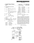
1
MICROCYBER HT1200M User Manual HART Modem ASIC (According to HCF_SPEC-54) Version: 1.1 Date: 07.12 V1.1 HT1200M User Manual Copyright and Disclaimer Copyright 2007 SIA. All rights reserved. The information in this document is proprietary and confidential to SIA, and for its customers’ internal use. In any event, no part of this document may be reproduced or redistributed in any form without the express written consent of SIA. None of the information contained in this document constitutes an express or implied warranty by SIA as to the sufficiency, fitness or suitability for a particular purpose of any such information or the fitness, or suitability for a particular purpose, merchantability, performance, compatibility with other parts or systems, or any portion thereof, referred to in this document. SIA expressly disclaims all representations and warranties of any kind regarding the contents or use of the information, including, but not limited to, express and implied warranties of accuracy, completeness, merchantability, fitness for a particular use, or non-infringement. In no event will SIA be liable for any direct, indirect, special, incidental or consequential damages, including, but not limited to, lost profits, lost business or lost data resulting from any use of or reliance upon the information, whether or not SIA has been advised of the possibility of such damage. Shenyang Institute of Automation (SIA) No.114 Nanta Street, Dongling District, Shenyang, P.R.China, 110016 www.sia.cn MICROCYBER Page 2 of 19 V1.1 HT1200M User Manual Revision History Version 1.1 MICROCYBER Release Date 07.12.22 Detail of Changes First release Page 3 of 19 V1.1 HT1200M User Manual List of Contents General Description ..................................................................................................................5 Features .....................................................................................................................................5 Typical Application ...................................................................................................................6 Pin Assignment .........................................................................................................................6 Pin Description..........................................................................................................................8 Function Description...............................................................................................................10 Package Information ...............................................................................................................15 Characteristics.........................................................................................................................17 List of Tables Table 1 HT1200M Pin Descriptions.......................................................................................7 List of Figures Figure 1 Figure 2 Figure 3 Figure 4 Figure 5 Figure 6 Figure 7 Figure 8 Figure 9 Figure 10 Figure 11 HT1200M Hart Modem Typical Application...........................................................6 (a) 28Pin PLCC Pinout Package (b) 32Pin LQFP Pinout Package.......................6 Reset Timing............................................................................................................8 HT1200M Block Diagram .....................................................................................10 Demodulator Signal Timing................................................................................... 11 OTXA Waveform (1200 Hz).................................................................................. 11 OTXA Waveform (2200 Hz)..................................................................................12 Receive Schematic.................................................................................................13 (a) Crystal Oscillator (b) Oscillator ....................................................................14 LQFP32................................................................................................................15 PLCC28................................................................................................................16 MICROCYBER Page 4 of 19 V1.1 HT1200M User Manual General Description The HT1200M is a single-chip, CMOS modem for use in Highway Addressable Remote Transducer (HART) field instruments and masters. The modem and a few external passive components provide all of the functions needed to satisfy HART physical layer requirements including modulation, demodulation, receive filtering, carrier detect and transmit-signal shaping. The HT1200M is pin-compatible with the SYM20C15. See the Pin Description and Functional Description sections for details on pin compatibility with the SYM20C15. The HT1200M uses Phase Continuous Frequency Shift Keying (FSK) at 1200 bits per second. To conserve power the receive circuits are disabled during transmit operations and vice versa. This provides the half-duplex operation used in HART communications. Features Can be used in designs presently using the SYM20C15 or equivalent type chip Single-chip, half-duplex 1200 bits per second FSK modem Bell 202 shift frequencies of 1200 Hz and 2200 Hz 3.3V-5.0V power supply Transmit-signal wave shaping Receive band-pass filter Low power: optimal for intrinsically safe applications CMOS compatible Internal oscillator requires 460.8kHz crystal or ceramic resonator Meets HART physical layer requirements Industrial temperature range of -40 °C to +85 °C Available in a 28-pin PLCC and 32-pin LQFP packages MICROCYBER Page 5 of 19 V1.1 HT1200M User Manual Typical Application . Figure 1 HT1200M Hart Modem Typical Application Pin Assignment (a) (b) Figure 2 (a) 28Pin PLCC Pinout Package (b) 32Pin LQFP Pinout Package MICROCYBER Page 6 of 19 V1.1 HT1200M User Manual Table 1 HT1200M Pin Descriptions Signal TEST1 TEST2 TEST3 Type input — — PLCC 1 2 3 LQFP 28 29 31 TEST4 — 4 32 No connect. TEST5 input 5 1 Connect to Vss. INRESET input 6 2 Reset all digital logic when low TEST7 input 7 3 Connect to Vss. TEST8 input 8 4 Connect to Vss. TEST9 input 9 5 Connect to Vss. OTXA output 10 7 IAREF input 11 8 Modulated output transmit and transmit signal to 4-20mA loop. FSK modulated HART interface circuit. Analog reference voltage. ICDREF input 12 9 Carrier detect reference voltage. OCBIAS output 13 10 Comparator bias current. TEST10 input 14 11 Connect to Vss. VDDA power 15 13 Analog supply voltage. IRXA input 16 14 ORXAF output 17 15 FSK modulated HART receive signal from 4-20mA loop interface circuit Analog receiver filter input. IRXAC input 18 16 Analog receive comparator input. OXTL output 19 17 Crystal oscillator output. IXTL input 20 18 Crystal oscillator input. VSS ground 21 6,20 Ground. VDD power 22 21,30 Digital supply voltage. INRTS input 23 22 Request to send. ITXD input 24 23 TEST11 — 25 24 Input transmit data. Transmitted HART data stream from UART. No connect. ORXD output 26 25 OCD output 27 26 Received demodulated HART data to UART. Carrier detect output. TEST12 — 28 27 No connect. VSSA ground — 12,19 MICROCYBER Description Connect to Vss. No connect. No connect. Analog ground Page 7 of 19 V1.1 HT1200M User Manual Pin Description IAREF: Analog Reference Voltage This analog input sets the do operating point of the operational amplifiers and comparators and is usually selected to split the do potential between VDD and Vss. IAREF in DC Characteristics refer to Electrical Characteristics. ICDREF: Carrier Detect Reference Voltage This analog input controls at which level the carrier detect (OCD) becomes active. This is determined by the do voltage difference between ICDREF and IAREF. Selecting ICDREF-IAREF equal to 0.08 VDC will set the carrier detect to a nominal 100 mVp-p. INRESET: Reset Digital Logic When at logic low (VSS) this input holds all the digital logic in Reset. During normal operation INRESET should be at VDD. INRESET should be held low for a minimum of 10 ns after VDD=2.5 V as shown in Figure 3. Figure 3 Reset Timing INRTS: Request To Send This active-low input selects the operation of the modulator. OTXA is enabled when this signal is low. This signal must be held high during power-up. IRXA: Analog Receive Input This input accepts the 1200/2200 Hz signals from the external filter. IRXAC: Analog Receive Comparator Input This is the positive input of the carrier detect comparator and the receiver filter comparator. ITXD: Digital Transmit Input(CMOS) This input to the modulator accepts digital data in NRZ form. When ITXD is low, the modulator output frequency is 2200 Hz. When ITXD is high, the modulator output frequency is 1200 Hz. IXTL: Oscillator Input This input to the internal oscillator must be connected to a parallel mode 460.8 kHz MICROCYBER Page 8 of 19 V1.1 HT1200M User Manual ceramic resonator when using the internal oscillator or grounded when using an external 460.8 kHz clock signal. OCBIAS: Comparator Bias Current The current through this output controls the operating parameters of the internal operational amplifiers and comparators. For normal operation, OCBIAS current is set to 2.5 uA. OCD: Carrier Detect Output This output goes high when a valid input is recognized on IRXA. If the received signal is greater than the threshold specified on ICDREF for four cycles of the IRXA signal, the valid input is recognized. ORXAF: Analog Receive Filter Output This signal is the square wave output of the receiver high-pass filter. ORCD: Digital Receive Output (CMOS) This signal outputs the digital receive data. When the received signal (IRXA) is 1200 Hz, ORXD outputs logic high. When the received signal (IRXA) is 2200 Hz, ORXD outputs logic low. ORXD is qualified internally with OCD and is logic high when OCD is low. OTXA: Analog Transmit Output This output provides the trapezoidal signal controlled by ITXD. When ITXD is low, the output frequency is 2200 Hz. When ITXD is high, the output frequency is 1200 Hz. This output is active when INRTS is low and 0.5 VDD when INRTS is high. OXTL: Oscillator Output This output from the internal oscillator must be connected to an external 460.8 kHz clock signal or to a parallel mode 460.8 kHz ceramic resonator when using the internal oscillator. TEST(12: 1): Test Pin These are test pins. For normal operation, tie these signals as per Table1. VDD: Digital Power This is the power for the digital modem circuitry. VDDA: Analog Supply Voltage This is the power for the analog modem circuitry. VSS: Ground This is the analog and digital ground. MICROCYBER Page 9 of 19 V1.1 HT1200M User Manual VSSA: Analog Ground Analog Ground Function Description The HT1200M is a functional equivalent of the SYM20C15 HART Modem. It contains a transmit data modulator and signal shaper, carrier detect circuitry, analog receiver and demodulator circuitry and an oscillator, as shown in Figure 4. The internal HART modulates the transmit-signal and demodulates the receive signal. The transmit-signal shaper enables the HT1200M to transmit a HART compliant signal. The carrier is detected by comparing the receiver filter output with the difference between two external voltage references. The analog receive circuitry band-pass filters the received signal for input to the modem and the carrier detect circuitry. The oscillator provides the modem with a stable time base using either a simple external resonator or an external clock source. Figure 4 HT1200M Block Diagram HT1200M LOGIC The modem consists of a modulator and demodulator. The modem uses shift frequencies of nominally 1200 Hz (for a 1)and 2200 Hz (for a 0). The bit rate is1200 bits/second. Modulator The modulator accepts digital data in NRZ form at the ITXD input and generates the FSK modulated signal at the OTXA output. INRTS must be a logic low for the modulator to be active. Demodulator The demodulator accepts an FSK signal at the IRXA input and reproduces the original modulating signal at the ORXD output. The nominal bit rate is 1200 bits per second. Figure 5 illustrates the demodulation process. MICROCYBER Page 10 of 19 V1.1 HT1200M User Manual Figure 5 Demodulator Signal Timing The output of the demodulator is qualified with the carrier detect signal (OCD), therefore, only IRXA signals large enough to be detected (100 mVp-p typically) by the carrier detect circuit produce received serial data at ORXD. Maximum demodulator jitter is 12 percent of one bit given input frequencies within HART specifications, a clock frequency of 460.8 kHz (1.0 percent) and zero input (IRXA) asymmetry. TRANSMIT-SIGNAL SHAPER The transmit-signal shaper generates a HART compliant FSK modulated signal at OTXA. Figure 6 and Figure 7 show the transmit-signal forms of the HT1200M. For IAREF=1.235 VDC, OTXA will have a voltage swing from approximately 0.25 to 0.75 VDC. Figure 6 MICROCYBER OTXA Waveform (1200 Hz) Page 11 of 19 V1.1 HT1200M User Manual Figure 7 OTXA Waveform (2200 Hz) CARRIER DETECT CIRCUITRY The Carrier Detect Comparator shown in Figure 8 below generates logic low output if the IRXAC voltage is below ICDREF. The comparator output is fed into a carrier detect block. The carrier detect block drives the carrier detect output pin OCD high if INRTS is high and four consecutive pulses out of the comparator have arrived. OCD stays high as long as INRTS is high and the next comparator pulse is received in less than 2.5 ms. Once OCD goes inactive, it takes four consecutive pulses out of the comparator to assert OCD again. Four consecutive pulses amount to 3.33 ms when the received signal is 1200 Hz and to 1.82 ms when the received signal is 2200 Hz. ANALOG RECEIVER CIRCUITRY Voltage References The HT1200M requires two voltage references: IAREF and ICDREF. IAREF sets the do operating point of the internal operational amplifiers and comparators. A 1.235 VDC reference(Analog Devices AD589) is suitable as IAREF. The level at which OCD (carrier detect) becomes active is determined by the do voltage difference (ICDREF-IAREF). Selecting a voltage difference of 0.08 VDC will set the carrier detect to a nominal 100 mVp-p. Bias Current Resistor The HT1200M requires a bias current resistor to be connected between OCBIAS and Vss. The bias current controls the operating parameters of the internal operational amplifiers and comparators. The value of the bias current resistor is determined by the reference voltage IAREF and the following formula: ⎛ IAREF ⎞ ⎟⎟ RBIAS = ⎜⎜ ⎝ 2.5μA ⎠ MICROCYBER Page 12 of 19 V1.1 HT1200M User Manual The recommended bias current resistor is 500 ohm; when IAREF is equal to 1.235 VDC. In Figure 8 all external capacitor values have a tolerance of 15 percent and the resistors have a tolerance of 1 percent, except the 3 ohm; which has a tolerance of 15 percent. External to the HT1200M, the filter exhibits a three-pole, high-pass filter at 624 Hz and a one-pole, low-pass filter at 2500 Hz. Internally, the HT1200M has a high-pass pole at 35 Hz and a low-pass pole at 90 kHz. The low-pass pole can vary as much as 130 percent. The input impedance of the entire filter is greater than 150 ohm; at frequencies below 50 kHz. Figure 8 Receive Schematic OSCILLATOR The HT1200M requires a 460.8 kHz clock signal on OXTL. This can be provided by an external clock or external components may be connected to the HT1200M internal oscillator. Internal Oscillator Option The oscillator cell will function with either a 460.8 kHz crystal or ceramic resonator. A parallel resonant ceramic resonator can be connected between OXTL and IXTL. Figure 9 illustrates the crystal option for clock generation using a 460.8 kHz (1 percent tolerance) parallel resonant crystal and two tuning capacitors. The actual values of the capacitors may depend on the recommendations of the manufacturer of the resonator. Typically, capacitors in the range of 100 pF to 470pF are used. MICROCYBER Page 13 of 19 V1.1 HT1200M User Manual External Clock Option It may be desirable to use an external 460.8 kHz clock as shown in Figure 10 rather than the internal oscillator because of the high cost and low availability of ceramic resonators. In addition, the HT 1200M consumes less current when an external clock is used. Minimum current consumption occurs with the clock connected to OXTL and IXTL connected to VSS. (a) Figure 9 MICROCYBER (b) (a) Crystal Oscillator (b) Oscillator Page 14 of 19 V1.1 HT1200M User Manual Package Information Figure 10 LQFP32 MICROCYBER Page 15 of 19 V1.1 HT1200M User Manual Figure 11 PLCC28 MICROCYBER Page 16 of 19 V1.1 HT1200M User Manual Characteristics ABSOLUTE MAXIMUMS Symbol Parameter Min. Max. Units TA Ambient -40 +85 ℃ TS Storage Temperature -55 +150 ℃ Supply Voltage 2.7 5.5 V DC Input, Output -0.3 VDD+0.3 V 250 ℃ VDD VIN , VOUT TL Lead Temperature (soldering) DC CHARACTERISTICS (VDD = 2.7V to 5.5V, VSS = 0V, TA = -40C to +85C) Symbol Parameter VDD Min. VIL Input Voltage, Low 2.7-5.5V VIL INRESET、INRTS 2.7-3.3V 0.9 VIH Input Voltage 2.7-5.5V 0.7*VDD VIH INRESET、INRTS 2.7-3.3V 1.3 VOL Output Voltage, Low (IOL = -1.8mA) VOH Output Voltage, High (IOH = -1.8mA) Typical 1.2 Max. Units 0.3*VDD V 1.4 V V 1.8 2.3 V V 2.7-3.3V 0.4 V 2.7-3.3V VDD-1.0 CIN Input Capacitance Analog Input IRXA Digital Input IIL/IH Input Leakage Current ±5 µA IOLL Output Leakage Current ±5 µA IDD Power Supply Current (RBIAS=500kΩ,IAREF=1.235V) 170 200 µA 2.6 V IAREF Analog Reference 2.1 20.8 3.1 pF 3.3 5.0 3.3 5.0 1.2 1.235 2.5 ICDREF Carrier Detect Reference (IAREF=.08V) 1.15 V OCBIAS Comparator Bias Current (RBIAS=500kΩ, IAREF=1.235V) 2.5 µA MICROCYBER Page 17 of 19 V1.1 HT1200M User Manual AC CHARACTERISTICS (VDD = 2.7V to 5.5V, VSS = 0V, TA = -40C to +85C) Pin Name IRXA Description Min. Receive Analog Input Leakage Current Frequency-Mark(Logic 1) Frequency-Space(Logic 0) 1190 2180 ORXAF Output of the High-pass Filter Slew Rate Gain Bandwidth (GBW) Voltage Range IRXAC OTXA ORXD OCD Typical Max. Units 1200 2200 +/-150 1210 2220 nA Hz Hz VDD-0.15 V/µs kHz V/µs +/-500 nA 0.025 150 0.15 Carrier Detect & Receive Filter Input Leakage Current Modulator Output Frequency-Mark(Logic1) Frequency-Space(Logic0) Amplitude(IAREF1.235V) Slop Loading(IAREF=1.235V) Hz Hz mV p-p mV/µs kΩ 1196.9 2194.3 500 2.84 30 Receive Digital Output Rise/Fall Time ns 20 Carrier Detect Output Rise/Fall Time ns 20 MODEM CHARACTERISTIC (VDD = 2.7V to 5.5V, VSS = OV, TA = -40 C to +85 C) Parameter Demodulater Jitter Conditions 1.Input frequencies at 1200Hz+/-10Hz,2200Hz+/-20Hz 2.Clock frequency of 460.8kHz+/-0.1% 3.Input(HLXA) asymmetry,0 MICROCYBER Min. Typical Max. Units 12 % of 1 bit Page 18 of 19 V1.1 HT1200M User Manual CERAMIC RESONATOR - EXTERNAL CLOCK SPECIFICATIONS (VDD = 2.7V to 5.5V, VSS = OV, TA = -40 C to +85 C) Parameter Min. Resonator Tolerance Frequency External Clock Frequency Duty Cycle Amplitude MICROCYBER Typical Max. Units 1% % kHz 465.4 60 kHz % V 460.8 456.2 40 460.8 50 VOH-VOL Page 19 of 19