1
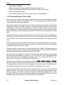
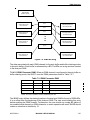
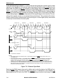
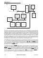
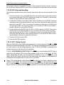
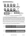
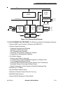
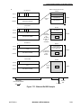
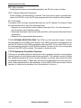
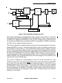
Serial Interface with Time Slot Assigner
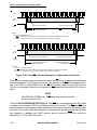
CTS2
CD2
BRG1
SCC1
RX
BRG2
BRG3
RCLK1
BRG4
BRGO1
BRGO2
BRGO3
BRGO4
SCC1
TX
TCLK1
SCC2
RX
RCLK2
SCC2
TX
TCLK2
CLK1
CLK2
BANK OF CLOCKS
SELECTION LOGIC
RCLK3
TCLK3
CLK3
CLK4
CLK5
CLK6
SCC3
RX
SCCS CONTROLLED IN THE SICR.
SMCS CONTROLLED IN SIMODE.
CLK7
CLK8
SCC3
TX
SCC4
RX
RCLK4
SCC4
TX
TCLK4
SMC1
SMC2
SMCLK1
SMCLK2
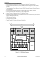
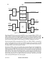
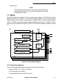
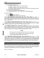
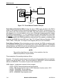
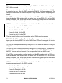
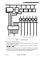
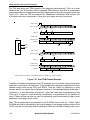
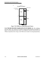
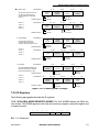
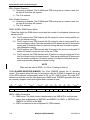
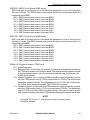
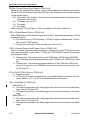
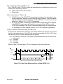
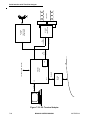
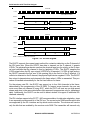
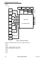
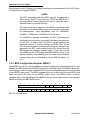
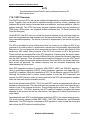
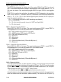
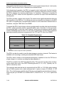
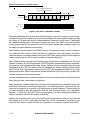
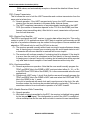
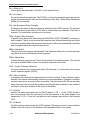
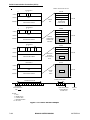
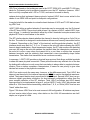
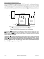
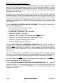
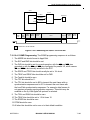
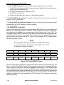
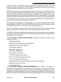
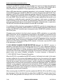
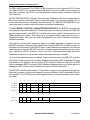
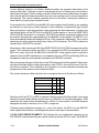
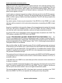
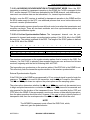
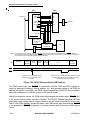
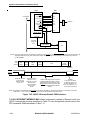
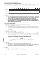
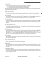
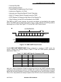
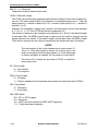
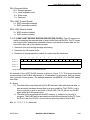
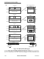
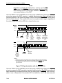
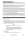
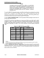
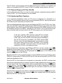
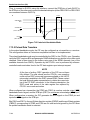
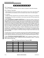
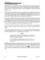
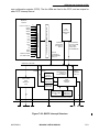
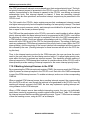
Figure 7-35. Bank of Clocks
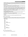
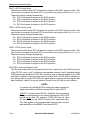
The SCC3 in NMSI mode has its own set of modem control pins:
TXD3
RXD3
TCLK3 <- BRG1–BRG4, CLK5–CLK8
RCLK3 <- BRG1–BRG4, CLK5–CLK8
RTS3
CTS3
CD3
7-102
MC68360 USER’S MANUAL
MOTOROLA