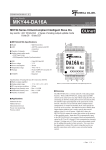
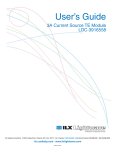
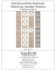
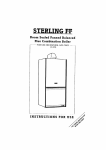
1
STD-MKY44-MC02A-V1.2E
Motion control function LSI for CUnet
MKY44-MC02A
User's Manual
Note
1. The information in this manual is subject to change without prior notice. Before using this
product, please confirm that this is the latest version of this manual.
2.Technical information in this manual, such as explanations and circuit examples, are
references for this product. When actually using this product, always fully evaluate
the entire system according to the design purpose based on considerations of
peripheral circuits and the PC board environment. We assume no responsibility for any
incompatibility between this product and your system.
3. We assume no responsibility whatsoever for any losses or damages arising from the use
of the information, products, and circuits in this manual, or for infringement of patents and
any other rights of a third party.
4.When using this product and the information and circuits in this manual, we do not
guarantee the right to use any property rights, intellectual property rights, and any other
rights of a third party.
5.This product is not designed for use in critical applications, such as life support systems.
Contact us when considering such applications.
6. No part of this manual may be copied or reproduced in any form or by any means without
prior written permission from StepTechnica Co., Ltd..
MKY44-MC02A User's Manual
Preface
This manual describes about “MKY44-MC02A”, motion control function LSI for CUnet.
The description of this manual is based on the premise that you have already understood the
overview of CUnet.
Be sure to read “CUnet Introduction Guide” before understanding this manual and the MKY44MC02A.
l Target Readers
This manual is for:
● Those who use StepTechnica's MKY44-MC02A to build the application used a CUnet
l Prerequisites
This manual assumes that you are familiar with:
● Network technology
● Semiconductor products (especially microcontrollers and memory)
l Related Manuals
● CUnet Introduction Guide Issued by: StepTechnica
● CUnet Technical Guide
Issued by: StepTechnica
[Caution]
Some terms in this manual are different from those used on our website and in our product
brochures. The brochure uses ordinary terms to help many people in various industries
understand our products.
Please understand technical information on HLS Family and CUnet Family based on technical
documents (manuals).
TM
n This manual has been prepared based on Standard English meeting the requirements of the International
Organization for Standardization (ISO) and the American National Standards Institute (ANSI). This English
manual is consistent with the Japanese document “STD-MKY44-MC02A-V1.2J”.
● Standard English is a trademark of Win Corporation.
---
iii ---
MKY44-MC02A User's Manual
CONTENTS
Chapter 1 Functions for Motion Control
1.1 Connection of MKY44-MC02A......................................................................................................1-3
1.2 Basic Instructions.........................................................................................................................1-4
1.2.1
Relationship between Basic Instructions and Parameters................................................1-4
1.2.2
Settable Speed.......................................................................................................................1-5
1.2.3
Setting Acceleration (Rate Format)......................................................................................1-5
1.2.4
Setting Acceleration (Required Time Format).....................................................................1-6
1.2.5
Parameter Auto Correction Function...................................................................................1-7
1.2.6
Selecting Speed Transition Curve........................................................................................1-7
1.2.7
256 Levels of Speed Transition............................................................................................1-8
1.2.8
Operation by Combination of Basic Instructions...............................................................1-8
1.2.9
Errors from Combination of Basic Instructions..................................................................1-9
1.2.10 Intentional Triangular Drive................................................................................................1-10
1.2.11 Triangular Drive Prevention Function................................................................................1-10
1.3 Move Instructions.......................................................................................................................1-12
1.3.1
Move Instruction to Specify Distance................................................................................1-13
1.3.2
Move Instruction to Specify Target....................................................................................1-14
1.3.3
Parameters of Move Instructions.......................................................................................1-15
1.3.4
Timing to Receive Move Instructions.................................................................................1-16
1.3.5
Operation of Move Instructions to Maintain Constant Speed..........................................1-16
1.3.6
Trapezoidal Speed Control and Pattern.............................................................................1-17
1.3.7
Relationship of Patterns......................................................................................................1-18
1.3.8
Pattern Reduction Function................................................................................................1-19
1.3.9
Usage Specifying Only Distance........................................................................................1-20
1.4 Origin Detection..........................................................................................................................1-21
1.4.1
Origin Search Instruction and Speed Transition..............................................................1-21
1.4.2
Three Origin Search Instructions and Their Detection Sensors.....................................1-22
1.4.3
Usage Example of the Origin Search Instruction and Initialization of Logical Coordinate Value......1-23
1.5 Stop Functions............................................................................................................................1-24
1.5.1
All Stop.................................................................................................................................1-25
1.5.2
DONA Stop............................................................................................................................1-25
1.5.3
Stop Using Origin Sensor, EZ Sensor, and Stop Signal Input.........................................1-25
1.5.4
Stop Using Stop Sensors and Hardware Limits...............................................................1-25
1.5.5
Physical Position Coordinate.............................................................................................1-26
1.5.6
Stop Setting Using Limit Coordinates...............................................................................1-26
1.6 Pattern Memory and File............................................................................................................1-27
1.7 Synchronization of Operation Instructions..............................................................................1-28
1.7.1
Synchronization Trigger......................................................................................................1-29
1.7.2
Synchronous Performance.................................................................................................1-29
1.7.3
Releasing Synchronization Wait State...............................................................................1-29
---
v ---
MKY44-MC02A User's Manual
1.8 Addressing Manual Operation...................................................................................................1-30
1.8.1
Continue Mode and Single Mode........................................................................................1-30
1.8.2
Speed and Distance in Manual Operation.........................................................................1-31
1.9 Utility Functions..........................................................................................................................1-32
1.9.1
Remote Reset from Applications........................................................................................1-32
1.9.2
General-Purpose Input Pins/General-Purpose Output Pins............................................1-32
1.9.3
Output Signal Indicating Axis Operating...........................................................................1-32
1.9.4
Do3 Watchdog Timer Function...........................................................................................1-33
1.9.5
Logical Inversion Function for Pins...................................................................................1-34
1.9.6
Addressing DONA and Network Failure............................................................................1-35
1.10 Registers for Motion Control.....................................................................................................1-36
Chapter 2 How to Use MKY44-MC02A
2.1 How to Access CUnet Interface and Registers..........................................................................2-4
2.1.1
How to Read Registers..........................................................................................................2-5
2.1.2
How to Write to Registers.....................................................................................................2-6
2.1.3
Cautions in Write Operation..................................................................................................2-7
2.1.4
Cautions in Read Operation..................................................................................................2-8
2.1.5
Warnings and Notifications from MKY44-MC02A...............................................................2-9
2.1.5.1 Reset Warning State and How to Cancel It.....................................................................2-9
2.1.5.2 CUnet Line Return Warning and How to Cancel It.......................................................2-10
2.1.5.3 Error Notification............................................................................................................2-10
2.1.5.4 Stop Notification (Optional)...........................................................................................2-11
2.1.5.5 Cautions for Warnings and Notifications..................................................................... 2-11
2.1.6
Extended CUnet Interface (Optional).................................................................................2-12
2.1.7
Processing Order of Access...............................................................................................2-13
2.1.8
Warnings of Setting Mistakes of SA and DOSA................................................................2-13
2.2 Internal Registers of MKY44-MC02A.........................................................................................2-14
2.2.1
Register Structure for Motion Control...............................................................................2-15
2.2.2
Write-Protected Registers...................................................................................................2-16
2.2.3
Descriptions of Registers for Motion Control...................................................................2-17
2.2.3.1 Description of Register AXS..........................................................................................2-17
2.2.3.2 Description of Register LPC..........................................................................................2-18
2.2.3.3 Description of Register PPC..........................................................................................2-18
2.2.3.4 Description of Register NS............................................................................................2-18
2.2.3.5 Description of Register COM.........................................................................................2-19
2.2.3.6 Description of Register TPC..........................................................................................2-20
2.2.3.7 Description of Register RAD..........................................................................................2-20
2.2.3.8 Descriptions of Registers LS and US...........................................................................2-21
2.2.3.9 Description of Register ACC..........................................................................................2-21
2.2.3.10 Description of Register SCom.......................................................................................2-22
2.2.3.11 Description of Register STS..........................................................................................2-22
2.2.3.12 Description of Registers PLC and MLC........................................................................2-23
---
vi ---
MKY44-MC02A User's Manual
2.2.3.13 Description of Register PG1..........................................................................................2-23
2.2.3.14 Description of Register PG2..........................................................................................2-24
2.2.4
Initial Values of Registers...................................................................................................2-26
2.3 Commands of MKY44-MC02A....................................................................................................2-27
2.3.1
Commands to Control Motion.............................................................................................2-28
2.3.2
Commands to Set Data in General-Purpose Output Pins................................................2-28
2.3.3
Data Setting Commands for Write-Protected Registers...................................................2-28
2.3.4
Operation Commands of Pattern Memory.........................................................................2-29
2.3.5
Synchronization Commands..............................................................................................2-30
2.4 Errors and Error Notification.....................................................................................................2-31
2.5 Motion Events..............................................................................................................................2-33
2.6 Exceptional Operation................................................................................................................2-34
2.7 Operation Procedure of MKY44-MC02A....................................................................................2-35
2.7.1
Process after Power-on and Return from Reset...............................................................2-35
2.7.2
Confirming Chip Codes.......................................................................................................2-35
2.7.3
Initializing the Registers for Motion Control of Each Axis...............................................2-36
2.7.4
Initializing the Application Device......................................................................................2-36
2.7.5
Normal Operation.................................................................................................................2-36
2.7.6
Exit Operation......................................................................................................................2-36
2.8 Addressing CUnet Mail Function...............................................................................................2-37
Chapter 3 MKY44-MC02A Hardware
3.1 Pin Functions of MKY44-MC02A..................................................................................................3-4
3.2 Electrical Ratings of Pins.............................................................................................................3-6
3.3 Pin Assignment.............................................................................................................................3-8
3.4 Connection of Basic I/O Signals..................................................................................................3-9
3.4.1
Supply of Drive Clocks..........................................................................................................3-9
3.4.2
Supply of Hardware Reset Signal.........................................................................................3-9
3.4.3
Connection of Signal for Hardware Setting (Hexadecimal Setting Specifications).......3-10
3.4.4
Connection of Signal for Hardware Setting (Decimal Setting Specifications)............... 3-11
3.5 Connection of CUnet-related I/O Signals..................................................................................3-12
3.5.1
Recommended Network Connection.................................................................................3-12
3.5.2
Connection and Displayed States of LED Indicator Pins.................................................3-13
3.5.3
PING Signal..........................................................................................................................3-14
3.5.4
CYCT signal..........................................................................................................................3-14
3.6 I/O Signal of Axis Control Unit...................................................................................................3-15
3.6.1
Connection of Motion Control Output Signals..................................................................3-15
3.6.2
Input Signal Connection for Physical Position Coordinates...........................................3-17
3.6.3
Input Signal of Sensors.......................................................................................................3-18
3.6.4
General-Purpose Input (#Di0 to #Di3)................................................................................3-18
3.6.5
General-Purpose Output (Do0 to Do3)...............................................................................3-19
3.7 Example of Connection Circuit..................................................................................................3-20
3.8 Electrical Ratings........................................................................................................................3-21
---
vii ---
MKY44-MC02A User's Manual
3.9 Package Dimensions..................................................................................................................3-22
3.10 Recommended Soldering Conditions.......................................................................................3-23
3.11 Recommended Reflow Conditions............................................................................................3-23
Appendix
Appendix 1 CUnet Cycle Time Table.............................................................................................App-3
Appendix 2 File Contents of Flash ROM in Factory Default Setting..........................................App-4
---
viii ---
MKY44-MC02A User's Manual
Figures
Fig. 1.1
Connection of MKY44-MC02A..................................................................................................1-3
Fig. 1.2
Method of Setting the Required Time.....................................................................................1-6
Fig. 1.3
Curve Selection.........................................................................................................................1-7
Fig. 1.4
256 Levels of Speed Transition................................................................................................1-8
Fig. 1.5
Driving by Combination of Basic Instructions.......................................................................1-8
Fig. 1.6
Examples of Intentional Triangular Drive.............................................................................1-10
Fig. 1.7
Triangular Drive Prevention with Peak Keep Time..............................................................1-10
Fig. 1.8
Driving Slide Table..................................................................................................................1-12
Fig. 1.9
Up/Down Counter Comprising Logical Position Coordinates............................................1-12
Fig. 1.10 Examples of Move Instructions Specifying Distance..........................................................1-13
Fig. 1.11 Examples of Move Instructions Specifying Target..............................................................1-14
Fig. 1.12 Move Instructions to Maintain Constant Speed...................................................................1-16
Fig. 1.13 Trapezoidal Speed Control.....................................................................................................1-17
Fig. 1.14 Relationships between Distance and Patterns....................................................................1-18
Fig. 1.15 Pattern Reduction...................................................................................................................1-19
Fig. 1.16 Speed Transition of Origin Search........................................................................................1-21
Fig. 1.17 Stop by Detecting the Sensor of Origin Search 1................................................................1-22
Fig. 1.18 Stop by Detecting the Sensor of Origin Search 2................................................................1-22
Fig. 1.19 Usage Example of Origin Search Instruction.......................................................................1-23
Fig. 1.20 Sensors and Signals of Stop System....................................................................................1-24
Fig. 1.21 Up/Down Counter Comprising Physical Position Coordinates..........................................1-26
Fig. 1.22 Pattern Memory.......................................................................................................................1-27
Fig. 1.23 Example of Operation Instruction.........................................................................................1-28
Fig. 1.24 Continue Mode and Single Mode...........................................................................................1-30
Fig. 1.25 Timing of DONA.......................................................................................................................1-35
Fig. 2.1
CUnet I/F Image........................................................................................................................2-4
Fig. 2.2
How to Write..............................................................................................................................2-6
Fig. 2.3
Extended Interface..................................................................................................................2-12
Fig. 2.4
Register Numbers and Registers..........................................................................................2-14
Fig. 2.5
Register Structure for Motion Control..................................................................................2-15
Fig. 2.6
Data Format of Remote Reset................................................................................................2-34
Fig. 3.1
Block Diagram of MKY44-MC02A............................................................................................3-3
Fig. 3.2
Pin electrical characteristics in I/O circuit types of MKY44-MC02A.....................................3-7
Fig. 3.3
Signal Assignment of MKY44-MC02A Pins.............................................................................3-8
Fig. 3.4
Connection of DIP-SW and Read-Only LSI (Hexadecimal Setting Specifications)...........3-10
Fig. 3.5
Connection of DIP-SW and Read-only LSI (Decimal Setting Specifications).................... 3-11
Fig. 3.6
Recommended Network Connection....................................................................................3-12
Fig. 3.7
Example Output Circuit to Ensure Initial Low-level ............................................................3-15
Fig. 3.8
Motion Control Output Signal of Positive/Negative Rotation.............................................3-16
Fig. 3.9
Example of Circuit Conversion for CW and CCW Pulse Format........................................3-16
Fig. 3.10 Example of Circuit Conversion from Phase Signal Format................................................3-17
Fig. 3.11 Example of MKY44-MC02A Circuit Connection...................................................................3-20
---
ix ---
MKY44-MC02A User's Manual
Tables
Table 1-1
Move Instructions..................................................................................................................1-3
Table 1-2
Parameters Required for Basic Instructions.......................................................................1-4
Table 1-3
Speed Range and Corresponding Speed............................................................................1-5
Table 1-4
Settable Acceleration.............................................................................................................1-5
Table 1-5
Example of Setting Acceleration Using Required Time Format........................................1-6
Table 1-6
Combinations of Basic Operation Instructions...................................................................1-9
Table 1-7
Combinations of Basic Instructions when Triangular Drive Function is ON................. 1-11
Table 1-8
Parameters Required for Move Instructions.....................................................................1-15
Table 1-9
Auto Start Enable Function.................................................................................................1-20
Table 1-10 Origin Search Instructions and Target Sensors................................................................1-22
Table 1-11 Factory Default Setting of Stop Functions........................................................................1-24
Table 1-12 Synchronous Performance.................................................................................................1-29
Table 1-13 Addressing Manual Operation............................................................................................1-31
Table 1-14 General-Purpose I/O Pins and Convertible Functions.....................................................1-32
Table 1-15 Pins Settable for Logical Inversion....................................................................................1-34
Table 1-16 Registers for Motion Control..............................................................................................1-36
Table 2-1
Description of AXS...............................................................................................................2-17
Table 2-2
Description of COM..............................................................................................................2-19
Table 2-3
Description of SCom...........................................................................................................2-22
Table 2-4
Settings of PG1....................................................................................................................2-23
Table 2-5
Factory Default Settings of PG1.........................................................................................2-23
Table 2-6
Settings of PG2....................................................................................................................2-24
Table 2-7
Factory Default Settings of PG2.........................................................................................2-25
Table 2-8
Initial Value of Each Register after Returning from Reset...............................................2-26
Table 2-9
List of Commands................................................................................................................2-27
Table 2-10 List of Synchronization Commands...................................................................................2-30
Table 2-11 List of Error Codes..............................................................................................................2-31
Table 2-12 List of Motion Event Codes.................................................................................................2-33
Table 3-1
Pin Functions of MKY44-MC02A...........................................................................................3-4
Table 3-2
Electrical Ratings of MKY44-MC02A....................................................................................3-6
Table 3-3
Settings of the DIP-SW Connected to ST44SW of Hexadecimal Setting Specifications.......3-10
Table 3-4
States of MKY44-MC02A Displayed by LED Indicators....................................................3-13
Table 3-5
General-Purpose I/O Pin and Shared Functions...............................................................3-18
Table 3-6
Absolute Maximum Ratings................................................................................................3-21
Table 3-7
Electrical Ratings.................................................................................................................3-21
---
x ---
Chapter 1 Functions for Motion Control
This chapter describes the functions for motion control provided by MKY44-MC02A.
1.1 Connection of MKY44-MC02A.......................................................................................... 1-3
1.2 Basic Instructions............................................................................................................. 1-4
1.3 Move Instructions............................................................................................................ 1-12
1.4 Origin Detection.............................................................................................................. 1-21
1.5 Stop Functions................................................................................................................ 1-24
1.6 Pattern Memory and File................................................................................................. 1-27
1.7 Synchronization of Operation Instructions.................................................................. 1-28
1.8 Addressing Manual Operation....................................................................................... 1-30
1.9 Utility Functions.............................................................................................................. 1-32
1.10 Registers for Motion Control.......................................................................................... 1-36
Chapter 1 Functions for Motion Control
Chapter 1 Functions for Motion Control
This chapter describes the functions for motion control provided by MKY44-MC02A. As this chapter focuses
on the concepts of functions and description of operations, please refer to the other chapters regarding actual use
after understanding this chapter.
1.1 Connection of MKY44-MC02A
CUnet is a network that can connect multiple devices. MKY44-MC02A is a CUnet-dedicated LSI for motion
control with the function to output pulse signals to drive a stepping motor or such.
MKY44-MC02A is connected between CUnet and a motor driver (motor amplifier) (see Figure 1.1).
MKY44-MC02A controls two axes using basic instructions and move instructions received from CUnet (see
Table 1-1).
Fig. 1.1 Connection of MKY44-MC02A
Table 1-1 Move Instructions
Basic instructions
Move instructions
Instruction
Name
Actual operation
Select Direction
CW, CCW
Select rotation direction. This operation can be executed only while stopped.
Stop
Quick_Stop
Stop pulse output.
Lower Speed
LFlat
Start pulse output at equal intervals corresponding to the lower speed.
Upper Speed
UFlat
Start pulse output at equal intervals corresponding to the upper speed.
Accelerate
P_Accele
Change the pulse output speed from the lower speed to the upper speed if stopped or from
the current speed to the upper speed if during operation.
Decelerate
M_Accele
Change the pulse output speed from the current speed to the lower speed.
Deceleration Stop
MA_Stop
Stop pulse output after changing the pulse output speed from the current speed to the lower
speed.
Distance specification pattern
movement
DS_Pattern
Output pulse of specified distance by changing the speed from stop to acceleration,
constant upper speed, and deceleration stop.
Distance specification
lower speed movement
DS_LFlat
Output pulse at equal intervals corresponding to the lower speed, equivalent to the
specified distance.
Distance specification
upper speed movement
DS_UFlat
Output pulse at equal intervals corresponding to the upper speed, equivalent to the
specified distance.
Target specification pattern
movement
TS_Pattern
Output pulse to the target position coordinate by changing the speed from stop to
acceleration, constant upper speed, and deceleration stop.
Target specification
lower speed movement
TS_LFlat
Output pulse at equal intervals corresponding to the lower speed. The number of pulses
output is equivalent to the distance to the target position coordinate.
Target specification
upper speed movement
TS_UFlat
Output pulse at equal intervals corresponding to the upper speed. The number of pulses
output is equivalent to the distance to the target position coordinate.
Origin detection
OriginSearch
Output the automatically calculated number of pulses to the origin orientation. Pulse
output stops upon sensor detection.
1-3
MKY44-MC02A User's Manual
1.2 Basic Instructions
This section describes basic instructions controlling axes.
1.2.1 Relationship between Basic Instructions and Parameters
There are seven basic instructions including Select Direction, Stop, Lower Speed, Upper Speed, Accelerate,
Decelerate, and Deceleration Stop. The parameters required for these instructions are lower speed, upper speed,
acceleration, and direction (see Table 1-2).
Table 1-2 Parameters Required for Basic Instructions
Instruction
Name
Lower speed
Upper Speed
Acceleration
Direction
Select Direction
CW, CCW
---
---
---
---
Stop
Quick_Stop
---
---
---
---
Lower Speed
LFlat
○
---
---
○
Upper Speed
UFlat
---
○
---
○
Accelerate
P_Accele
○
○
Decelerate
M_Accele
○
---
○
□
Deceleration Stop
MA_Stop
○
---
○
□
○: A parameter is required to execute the instruction.
: Required to start the operation of a stopped axis with the Accelerate instruction.
When it is already operating, the current set value applies.
□: The current set value applies since the execution of the instruction is enabled only during operation.
These seven basic instructions will not be executed unless all the required parameters are newly set. The
parameters set previously can be used again if changes are not necessary.
The parameters of lower speed, upper speed, and acceleration can be rewritten to prepare for the next instruction
even during instruction execution.
When “Deceleration Stop” is selected as the stop style for MKY44-MC02A, rewriting the parameters of lower
speed and acceleration is disabled during operation. In such a case, if the lower speed parameter is rewritten
mistakenly, an error showing that it is disabled will occur. For more information about stop type, see “1.5
Stop Functions”.
1-4
Chapter 1 Functions for Motion Control
1.2.2 Settable Speed
MKY44-MC02A has three speed ranges, as shown in Table 1-3.
The speed range should be selected while the axis is stopped. It is
generally recommended to select it at the initial setting of the system.
Table 1-3 Speed Range and
Corresponding Speed
Speed range
Corresponding speed
2, 3
160 pps to 12.5 kpps
1
40 pps to 10.0 kpps
0
10 pps to 2.5 kpps
The parameters of lower speed and upper speed can be set flexibly in
units of 1 pps within the selected range.
MKY44-MC02A doesn’t have the concept of “magnification”
commonly seen in 1-chip type pulse generator LSIs. For example, when the speed range from 160 pps to 12.5
kpps is selected, the lower speed can be set as 234 pps and the upper speed can be set as 8,765 pps. This is
useful for speed specification avoiding mechanical resonance and for speed specification in flow control.
The precision of speed setting of MKY44-MC02A is within ±0.3%.
The factory default speed range is “2 (160 pps to 12.5 kpps)”.
1.2.3 Setting Acceleration (Rate Format)
Although acceleration is commonly represented as “the amount of speed change in a second (pps/sec or pps2)”,
With MKY44-MC02A, the value is set as “the amount of speed change in 10 ms (pps/10 ms)” (see Table 1-4).
Acceleration includes plus acceleration
(acceleration) in which the speed transitions to the
upper speed and minus acceleration (deceleration)
in which the speed transitions to the lower speed.
Plus acceleration and minus acceleration can be
set individually. The values that can be set with
MKY44-MC02A are 1 to 1,542.
Table 1-4 Settable Acceleration
MKY44-MC02 setting
value (pps/10 ms)
Common acceleration
indication
(pps/sec)
Reference
indication
(ms/kHz)
---
to 99
---
1
100
10,000
2
200
5,000
5
500
2,000
10
1K
1,000
20
2K
500
50
5K
200
100
10 K
100
200
20 K
50
500
50 K
20
1,000
100 K
10
1,542
154.2 K
≈6.5
---
154.3 K to
---
If the required time (speed transition width ÷
rate) for speed transition exceeds 40.95 seconds
when acceleration is very slow and speed
transition width is large, the acceleration will be
set for 40.95 seconds. Also, if the acceleration
is high and the required time for speed transition
is less than 80 ms when executing acceleration/
deceleration, an error will occur.
Even if the required time for speed transition is less than 80 ms, an error will not occur when the function
described in “1.2.5 Parameter Auto Correction Function” is on; the acceleration will be forced so that the
required time for speed transition is 80 ms.
1-5
MKY44-MC02A User's Manual
1.2.4 Setting Acceleration (Required Time Format)
The time to transition between the upper
speed and the lower speed, i.e. the required
climbing time (acceleration) and falling time
(deceleration), can be used as a format for
setting acceleration (see Figure 1.2). In the
factory default setting, rate format is selected
instead of required time format. To use values
in the required time format, set the ARTS
(Acceleration Rate/Time Select) bit of the PG2
(Property Group 2) register.
Fig. 1.2 Method of Setting the Required Time
In this setting, values with units of 10 ms are
set. For example, set “100” for “1 second”
and set “1,000” for “10 seconds”. Plus acceleration and minus acceleration can be set individually, just like the
standard method. The values that can be set regardless of upper speed are 8 to 4,095 (0.08 seconds to 40.95
seconds). To illustrate this method, settings where the transition width is 8 kpps or 12.34 kpps are shown in
Table 1-5. This setting method is easy to use for changing speed gently within a predetermined range, such as
for flow control, including air and water flows.
Table 1-5 Example of Setting Acceleration Using Required Time Format
When the acceleration is from 500 pps
(lower speed) to 8.5 kpps (upper speed)
(500 to 8.5 kpps: D8,000 pps)
When the acceleration is from 160 pps
(lower speed) to 12.5 kpps (upper speed)
(160 to 12.5 kpps: D12,340 pps)
Reference indication
Transition time
Setting value
Transition time
Setting value
pps/10 ms
pps/sec
ms/kHz
*40.95 seconds
4,095 (0xFFF)
*40.95 seconds
4,095 (0xFFF)
---
to 99
---
*40.95 seconds
4,095 (0xFFF)
*40.95 seconds
4,095 (0xFFF)
1
100
10,000
40.00 seconds
4,000 (0xFA0)
*40.95 seconds
4,095 (0xFFF)
2
200
5,000
---
---
40.95 seconds
4,095 (0xFFF)
≈3
≈300
≈3,000
16.00 seconds
1,600(0x640)
24.68 seconds
2,468 (0x9A4)
5
500
2,000
8.00 seconds
800 (0x320)
12.34 seconds
1,234 (0x4D2)
10
1K
1,000
4.00 seconds
400 (0x190)
6.17 seconds
617 (0x269)
20
2K
500
1.60 seconds
160 (0x0A0)
≈2.47 seconds
247 (0x0F7)
50
5K
200
0.80 seconds
80 (0x050)
≈1.23 seconds
123 (0x07B)
100
10 K
100
0.4 seconds (400 ms)
40 (0x028)
≈0.62 seconds (620 ms)
62 (0x03E)
200
20 K
50
0.16 seconds (160 ms)
16 (0x010)
≈0.25 seconds (250 ms)
25 (0x019)
500
50 K
20
0.08 seconds (80 ms)
8 (0x008)
≈0.12 seconds (120 ms)
12 (0x00C)
1,000
100 K
10
---
---
≈0.08 seconds (80 ms)
8 (0x008)
1,542
154.2 K
≈6.5
---
---
---
---
---
154.3 K up
---
When the upper speed is lower than or equal to 11 kpps, “7 (70 ms: 0.07 seconds)” can be set as the minimum time.
When the upper speed is lower than or equal to 8 kpps, “6 (60 ms: 0.06 seconds)” can be set as the minimum time.
When the upper speed is lower than or equal to 5 kpps, “5 (50 ms: 0.05 seconds)” can be set as the minimum time.
In the factory default setting, the required time format is not selected. In the table, “*” indicates the maximum
settable value.
1-6
Chapter 1 Functions for Motion Control
1.2.5 Parameter Auto Correction Function
If the acceleration setting of MKY44-MC02A goes out of the controllable range, whether in the standard rate
format or the optional required time format, an error will occur when an operation instruction is received. It is
the same when the setting of upper speed and lower speed is inappropriate.
In such a case, there is a “parameter auto correction function” that can automatically correct the setting into the
controllable range without causing any errors. For example, when the speed range is “2”, an error will occur if “40
pps” is mistakenly set as the lower speed. However, if the “parameter auto correction function” is on, the lower
speed setting will be changed automatically to “160 pps”, which is the minimum value of the “2” speed range.
In this way, the function affects the parameter values of speed and acceleration.
When the speed transition width is less than “32” in the basic instructions Accelerate, Decelerate, and
Deceleration Stop, an error will occur even if “parameter auto correction function” is selected because the
transition width is too narrow. However, when the speed transition width is less than “32” in pattern move
instructions, described later, an error will not occur if “parameter auto correction function” is selected. This is
because the operation will be corrected automatically to the move instruction without speed transition by lower
speed.
Turn ON or OFF the “parameter auto correction function” using the PAC (Parameter Auto Correction) bit of the
PG2 (Property Group 2) register.
If a speed error occurs, the details will be shown by an error code.
For details on error codes, see “2.4 Errors and Error Notification”.
The parameter auto correction function is ON in the factory default setting.
1.2.6 Selecting Speed Transition Curve
In MKY44-MC02A, a straight line or S-curve can be selected for the speed transition of acceleration and
deceleration (see Figure 1.3).
The speed transition curve needs to be selected while stopped. It is generally recommended to select it at
the initial setting of the system. In MKY44-MC02A, it is not possible to set acceleration and deceleration
differently, e.g. “straight line for acceleration and S-curve for deceleration”. Set the speed transition using the
CS (Curve Select) bit of the PG1 (Property Group 1) register.
Fig. 1.3 Curve Selection
S-curve is set in the factory default setting.
1-7
MKY44-MC02A User's Manual
1.2.7 256 Levels of Speed Transition
The speed change between upper speed and lower speed in MKY44-MC02A has 256 levels with constant
transition time. For example, if the lower speed is set to 123 pps and the upper speed is set to 9,876 pps in an
S-curve with an acceleration rate of 5 kpps/sec (or acceleration required time of 1,950 ms) and an deceleration
rate of 25 kpps/sec (or acceleration required time of 390 ms), it will take 256 levels of transition to the target
speed for both acceleration and deceleration. This makes speed transition smooth regardless of the setting value
(see Figure 1.4).
Fig. 1.4 256 Levels of Speed Transition
To address a deceleration instruction while accelerating, it will decelerate by the same number of levels used
by acceleration because the speed transition width is not the width between the upper speed and the lower
speed. It is the same for addressing an acceleration instruction while decelerating.
1.2.8 Operation by Combination of Basic Instructions
Basic instructions can be used in serial combination. Figure 1.5 shows an example.
Fig. 1.5 Driving by Combination of Basic Instructions
1-8
Chapter 1 Functions for Motion Control
1.2.9 Errors from Combination of Basic Instructions
MKY44-MC02A defines importance in the order “Stop > Deceleration Stop > Other instructions”. Therefore,
when it receives a “Stop” instruction, it will stop regardless of operation status (see Table 1-6).
The “Deceleration Stop” instruction comes right next to the “Stop” instruction in importance. While performing
the deceleration, an important stop process in the “Deceleration Stop” instruction, other instructions such
as “Lower Speed”, “Upper Speed”, “Accelerate”, and “Decelerate” will not be accepted but cause an error.
With MKY44-MC02A, an error will occur for some combinations, such as “Accelerate” instructions while
accelerating. Errors caused by ×-marked operations in Table 1-6 are only to notify that instructions will not be
accepted. They will not affect operations in execution.
Table 1-6 Combinations of Basic Operation Instructions
Instruction
At upper speed
At lower speed
While
accelerating
While
decelerating
While
decelerating by
deceleration
stop instruction
While stopped
Select Direction
×
×
×
×
○
Stop
○
○
○
○
○
Lower Speed
○
○
○
×
○
Upper Speed
○
○
○
×
○
Accelerate
○
×
○
×
○
Decelerate
○
○
×
×
×
Deceleration Stop
○
○
□
□
×
○:Can be executed.
□:Stop as soon as deceleration ends: already decelerating.
×:An error will occur and the instructions will not be executed. It will not affect operations in
execution.
If an error occurs, the details will be shown by an error code.
For details on error codes, see “2.4 Errors and Error Notification”.
1-9
MKY44-MC02A User's Manual
1.2.10 Intentional Triangular Drive
By executing the “Decelerate” instruction while accelerating, you can intentionally execute a triangular drive
which forms an angle at the upper speed side. Similarly, by executing the “Accelerate” instruction while
decelerating, you can intentionally execute a triangular drive which forms an angle at the lower speed side (see
Figure 1.6). These intentional triangular drives can be used to effectively control some mechanisms.
Fig. 1.6 Examples of Intentional Triangular Drive
1.2.11 Triangular Drive Prevention Function
If a machine is shifted to deceleration while it is still accelerating, the drive systems such as motors, gear boxes,
and actuators may be overloaded. Therefore, it is generally required to prevent this except for some applications
that allow triangular drive.
MKY44-MC02A can insert “Peak Keep Time”, which can retain the speed at which triangular drive occurs for a
certain period of time (see Figure 1.7). As well as during acceleration and deceleration, “Peak Keep Time” can
be applied at the upper speed after acceleration, at the lower speed after deceleration, and while stopped after
deceleration stop. Peak Keep Time can be set in units of 10 ms up to 10.23 seconds (0x3FF) with the PKTS (Peak
Keep Time Setup) bit of the PG1 (Property Group 1) register. The setting of Peak Keep Time as “0” is the OFF
state of the triangular drive prevention function. The factory default setting is OFF.
Fig. 1.7 Triangular Drive Prevention with Peak Keep Time
1-10
Chapter 1 Functions for Motion Control
The combinations of basic instructions when a value other than “0” is set in Peak Keep Time and the triangular
drive prevention function is ON are shown in Table 1-7.
When the triangular drive prevention function is ON, it will start a deceleration stop operation after the time
necessary for forming “Peak Keep Time” is inserted, even if the “Deceleration Stop” instruction is received
or the limit coordinate set as the start position of deceleration stop is reached while accelerating or at the
upper speed after acceleration. Also, an error will occur if the “Accelerate” instruction is received before the
end of “Peak Keep Time” after deceleration stop. Therefore, it is recommended not to set “Peak Keep Time”
unnecessarily long.
Table 1-7 Combinations of Basic Instructions when Triangular Drive Function is ON
Instruction
At upper speed
At lower speed
While
accelerating
While
decelerating
While
decelerating by
deceleration
stop instruction
While stopped
Select Direction
×
×
×
×
○
Stop
○
○
○
○
○
Lower Speed
○
○
○
×
○
Upper Speed
○
○
○
×
○
Accelerate
○ (▲)
×
▲
×
○ (×)
Decelerate
○ (▼)
▼
×
×
×
Deceleration Stop
○ (▼)
▼
□
□
×
○: Can be executed.
□: Stop as soon as deceleration ends: already decelerating.
×: An error will occur and the instructions will not be executed.
▲:If the time at constant speed is shorter than the time set for Peak Keep Time at the point
time when a instruction is received, it will start accelerating after inserting enough time
form Peak Keep Time.
▼:If the time at constant speed is shorter than the time set for Peak Keep Time at the point
time when a instruction is received, it will start decelerating after inserting enough time
form Peak Keep Time.
1-11
in
to
in
to
MKY44-MC02A User's Manual
1.3 Move Instructions
This section describes move instructions.
Most applications using stepping motors manage and control the number of rotations of the motors and the
distance of the actuators driven by the motors. For example, to drive a slide table using a stepping motor,
positive rotation of the motor moves the table in the positive direction the same distance the motor rotates.
Conversely, negative rotation of the motor moves the table in the negative direction the same distance the motor
rotates (see Figure 1.8).
Fig. 1.8 Driving Slide Table
In such an application, the signal of rotation direction output by MKY44-MC02A moves the table in a certain
direction, and the pulse count output by MKY44-MC02A corresponds to the distance of the table. If an Up/
Down counter is set up by adding the pulse count when the rotation direction is positive (CW: ClockWise) and
subtracting the pulse count when it is negative (CCW: CounterClockWise), the value of the Up/Down counter
will correspond to the coordinate of the table position (see Figure 1.9).
Fig. 1.9 Up/Down Counter Comprising Logical Position Coordinates
MKY44-MC02A has an Up/Down counter that can create coordinates from the number of pulse signals output
by the LSI. The value of this counter is called “Logical Position Coordinates” (LPC).
Since the Up/Down counter of MKY44-MC02A is 24-bit, signed, the available coordinate values are “-8,388,608
to 8,388,607 (0x800000 to 0x7FFFFF)”. There are two types of move instructions that can take specifications
of distance and target position based on these “logical position coordinates” in MKY44-MC02A.
1-12
Chapter 1 Functions for Motion Control
1.3.1 Move Instruction to Specify Distance
One of the two types of move instructions is Distance Specification (DS), which specifies “how much distance
to move” relative to the current logical position coordinates. This type of instruction includes the following
three movements.
1. Distance specification pattern movement (DS_Pattern)
There are two types of distance, “Relative
Distance (RD)” and “Absolute Distance
3. Distance specification upper speed movement (DS_UFlat)
(AD)”. Both types provide 24-bit numerical
parameters to MKY44-MC02A. “Relative
Distance” can handle the numerical values of “-8,388,608 to 8,388,607 (0x800000 to 0x7FFFFF)” since it is
signed to indicate positive or negative direction. “Absolute Distance” can handle “0 to 16,777,215 (0x000000 to
0xFFFFFF)”, since it is unsigned. The usage of instructions specifying distance is illustrated in Figure 1.10.
2. Distance specification lower speed movement (DS_LFlat)
Fig. 1.10 Examples of Move Instructions Specifying Distance
When specifying distance, you need to set whether to use “relative distance” or “absolute distance” beforehand
using the RADS (Relative/Absolute Distance Select) bit of the PG2 (Property Group 2) register. It is generally
recommended to select it at the initial setting of the system.
If the position reached from specifying the distance exceeds the controllable range of logical position
coordinates, an error will occur.
However, in applications such as controlling a rotating system that constantly rotates in a certain direction, this
error is inappropriate. Therefore, you can select an option that enables over-scale distance so there will be no
error even if the position reached exceeds the controllable range of logical position coordinates. It can be set
with the OSE (Over Scale Enable) bit of the PG2 register.
“Relative distance” is selected in the factory default setting. Over-scale distance is disabled in this setting.
1-13
MKY44-MC02A User's Manual
1.3.2 Move Instruction to Specify Target
The other type of move instruction is Target Specification (TS), which specifies “Target Position Coordinates”.
This type of instruction includes the following three movements.
1. Target specification pattern movement (TS_Pattern)
The numerical values that can be handled
by “Target Position Coordinates (TPC)” are
3. Target specification upper speed movement (TS_UFlat)
the same as “Logical Position Coordinates”,
“-8,388,608 to 8,388,607 (0x800000 to
0x7FFFFF)”. Since rotation direction is naturally determined in move instructions specifying the target, there is
no need to set the rotation direction.
2. Target specification lower speed movement (TS_LFlat)
The usage of instructions specifying target is illustrated in Figure 1.11.
Fig. 1.11 Examples of Move Instructions Specifying Target
1-14
Chapter 1 Functions for Motion Control
1.3.3 Parameters of Move Instructions
Table 1-8 shows the parameters required for move instructions.
Table 1-8 Parameters Required for Move Instructions
Move instructions
Instruction
Name
Relative
distance
Target
position
coordinates
Distance specification
pattern movement
DS_Pattern
○
---
○
○
○
RD : --AD : ○
Distance specification
lower speed movement
DS_LFlat
○
---
○
---
---
RD : --AD : ○
Distance specification
upper speed movement
DS_UFlat
○
---
---
○
---
RD : --AD : ○
Target specification
pattern movement
TS_Pattern
---
○
○
○
○
---
Target specification
lower speed movement
TS_LFlat
---
○
○
---
---
---
Target specification
upper speed movement
TS_UFlat
---
○
---
○
---
---
Target
position
coordinates
Lower speed
Upper speed
Acceleration
Direction
Direction column
RD: Relative Distance specification
AD: Absolute Distance specification
This doesn’t mean that instructions will not be executed unless all the required parameters are newly set. The
parameters set previously can be used again if changes are not necessary.
However, if instructions specifying target are issued serially without changing the “target position coordinates”,
an error shows that no movement will occur. In contrast, instructions specifying distance can be executed
serially without changing any parameters.
Although direction parameters are necessarily determined in instructions specifying target and move instructions
specifying “Relative Distance (RD)”, a setting is required to execute move instructions using “Absolute Distance
(AD)”.
The parameters of relative distance, absolute distance, target position coordinate, lower speed, upper speed, and
acceleration can be rewritten to prepare for the next instruction even during instruction execution.
When “Deceleration Stop” is selected as a stop type option for MKY44-MC02A, rewriting the parameters
of lower speed and acceleration is disabled during operation. In such a case, if the lower speed parameter is
rewritten mistakenly, an error showing that it is disabled will occur. For more information about stop type, see
“1.5 Stop Functions”.
1-15
MKY44-MC02A User's Manual
1.3.4 Timing to Receive Move Instructions
The basic instructions Stop and Deceleration Stop will be received even while operating with move instructions
(Peak Keep Time may be inserted into the Deceleration Stop instruction with the triangular drive prevention
function).
In contrast, move instructions will be received only while stopped. While logical position coordinates are
transitioning, move instructions will not be received since the initial position for movement can hardly be
identified. If the user application mistakenly issues a move instruction during operation, MKY44-MC02A will
return an error saying that it will not receive the instruction.
1.3.5 Operation of Move Instructions to Maintain Constant Speed
Among the move instructions, the following four instructions move with constant speed.
1. Distance specification lower speed movement (DS_LFlat)
The part corresponding to the graphical area
of these speed transitions is the distance. For
3. Target specification lower speed movement (TS_LFlat)
example, the movement time required for a
4. Target specification upper speed movement (TS_UFlat)
“distance specification lower speed
movement (DS_LFlat)” instruction when the
lower speed is “1,000 pps” and the relative distance is “10,000” is “10 seconds” [10,000 ÷ 1,000]. The
movement time required for a “distance specification upper speed movement (DS_UFlat)” instruction when the
upper speed is “5,000 pss” and the relative distance is “10,000” is “2 seconds”. The distance in both cases is
“10,000” and the area of the diagram is also the same. Also, the distance matches the pulse count output by the
pulse output pin of MKY44-MC02A (see Figure 1.12).
2. Distance specification upper speed movement (DS_UFlat)
Fig. 1.12 Move Instructions to Maintain Constant Speed
1-16
Chapter 1 Functions for Motion Control
1.3.6 Trapezoidal Speed Control and Pattern
Among the move instructions, the following two instructions execute “trapezoidal speed control” for
acceleration from the lower speed to the upper speed, a period at the upper speed, and then deceleration to the
lower speed and stop (see Figure 1.13).
1. Distance specification pattern movement (DS_Pattern)
2. Target specification pattern movement (TS_Pattern)
Most stepping motors cannot start from upper
speed rotation because of structural features.
Therefore, it is common to use “trapezoidal
speed control” for driving a stepping motor.
The part corresponding to the graphical area of
“trapezoidal speed control” in a pattern move instruction is the distance. This distance matches the pulse count
output by the pulse output pin of MKY44-MC02A.
Trapezoidal speed control comes into effect when the target position coordinates or the parameters of distance,
lower speed, upper speed, and acceleration (plus and minus acceleration) are all available. With MKY44MC02A, a set of these parameters, or the figure of speed transition formed by a set of parameters, is called a
“pattern”.
Fig. 1.13 Trapezoidal Speed Control
1-17
MKY44-MC02A User's Manual
1.3.7 Relationship of Patterns
In basic trapezoidal speed control (see Figure 1.14 A), conceptually, there is no rules for the time to maintain
the upper speed. Therefore, the minimum distance forming the trapezoid is an area where the time of the upper
speed period is “0” (see Figure 1.14 B). Although this is no longer a trapezoid but intentional triangular drive,
MKY44-MC02A can execute pattern move instructions specifying the distance not less than this area.
For example, the theoretical value of distance required for pattern formation is (((500 + 4,500) x 4) ÷ 2) + (((500
+ 4,500) x 2) ÷ 2) = “15,000” according to the calculation method of the graphical area when it is set that lower
speed is “500 pps”, upper speed is “4,500 pps”, plus acceleration is “1,000 pps/sec (10 pps/10 ms)”, and minus
acceleration is “2,000 pps/sec (20 pps/10 ms)”.
Fig. 1.14 Relationships between Distance and Patterns
If the distance of “24,000”, which is more than the minimum distance forming the trapezoid, is commanded in
this pattern, a trapezoidal speed control where upper speed period of 2 seconds is inserted will be performed (see
Figure 1.14 C). If a distance less than the minimum distance to form the trapezoid (less than “15,000” in this
example) is instructed, MKY44-MC02A will return an error saying that the distance is not enough to form the
pattern.
If a value other than “0” is set for Peak Keep Time in order to enable the triangular drive prevention function,
the distance required for pattern formation will be increased by the distance that has Peak Keep Time as upper
speed period. In the example shown in Figure 1.14 D, where “3 seconds” is set for Peak Keep Time, the
minimum distance forming the trapezoid is “28,500”.
The values such as “15,000” and “28,500” described above are theoretical values. The values that become
errors are less than “15,019” and “28,520” with up to 0.2% calculation error.
1-18
Chapter 1 Functions for Motion Control
1.3.8 Pattern Reduction Function
Most applications using stepping motors try to avoid calculation of the minimum distance and errors caused
when they fall below it, except when controlling motor precisely and sensitively. If the lower speed, acceleration
rate, and distance (coordinates) are maintained, it is preferred not to return errors but to operate accurately to
some extent.
MKY44-MC02A has an optional function that operates reasonably adjusting the patterns without returning
errors when it receives pattern move instructions with less distance than the distance required for pattern
formation. This function is called “Pattern Reduction” function.
The pattern reduction function of MKY44-MC02A is not an equal ratio reduction of geometric graphics. It
adjusts the upper speed and upper speed period while maintaining the parameter values of lower speed and
acceleration
Figure 1.15 shows the reduction examples when the distance required for pattern formation is set to 80%, 60%,
40%, 20%, 10%, and 5%. The pattern reduction function can be used regardless of the type of speed curve,
the difference between acceleration rate and deceleration rate, and enabling/disabling of the triangular drive
prevention function.
Fig. 1.15 Pattern Reduction
If either of the following two reasons apply, the pattern reduction function of MKY44-MC02A will conclude
that the formation of trapezoidal speed control is inappropriate and perform the movement at the lower speed
without speed transition. This is only when the reduction rate becomes very high with little distance. “5%” in
Figure 1.15 is a example of this case.
(1) When the speed transition width of lower speed and upper speed is less than 32 pps
(2) When the required time for acceleration or deceleration is less than or equal to 8 ms
Turn ON/OFF the pattern reduction function using the PRE (Pattern Reduction Enable) bit of the PG2 (Property
Group 2) register.
“ON” is selected for the pattern reduction function in the factory default setting.
1-19
MKY44-MC02A User's Manual
1.3.9 Usage Specifying Only Distance
Auto Start Enable (ASE) function is one of the optional settings for MKY44-MC02A.
If this function is selected and the user application sets “relative distance” or “absolute distance”, the “distance
specification pattern movement (DS_Pattern)” instruction will be started simultaneously. Similarly, if the user
application sets “target position coordinate”, “target specification pattern movement (TS_Pattern)” will be
started simultaneously (see Table 1-9).
Table 1-9 Auto Start Enable Function
Parameter that triggers instruction execution
Instruction starting automatically
Relative distance
Absolute distance
Target position coordinate
Instruction
Name
○
---
---
---
○
---
Distance
specification pattern
movement
DS_Pattern
---
---
○
Target specification
pattern movement
TS_Pattern
An error will occur if this auto start enable option is selected and the speed parameter is inappropriate. By
turning on the parameter auto correction function, one can often avoid errors. For the details of the parameter
auto correction function, see “1.2.5 Parameter Auto Correction Function”.
If the most high-performance parameter available in the application environment is set and all the options
of auto start enable function, pattern reduction function, and parameter auto correction function are enabled,
the user application can easily control the motion by just setting the distance or the target position coordinate
parameters.
Set the auto start enable function using the ASE (Auto Start Enable) bit of the PG2 (Property Group 2) register.
In the factory default setting, the pattern reduction function is ON, the parameter auto correction function is
ON, and the auto start enable function is OFF.
1-20
Chapter 1 Functions for Motion Control
1.4 Origin Detection
This section describes origin detection.
Since the application for controlling distance controls using logical coordinates, the logical coordinate itself
requires some sort of control point. In most applications using stepping motors, an origin sensor is set up and
the position detected by the sensor is set as a control point where the value of logical coordinate is “0”.
1.4.1 Origin Search Instruction and Speed Transition
MKY44-MC02A has an origin search instruction. This instruction causes movement for the absolute distance
of [current logical coordinate position + (lower speed ÷ 2)] from the current logical coordinate position to the
direction of logical coordinate “0”. The origin search instruction causes movement according to the current
parameters of upper speed, lower speed, plus acceleration, minus acceleration, acceleration/deceleration curve
selection, and triangular drive prevention function.
Only the origin search instruction can make the pattern reduction function work even if the pattern reduction
function option is OFF. Similarly, only the origin search instruction can make the parameter auto correction
function work even if parameter auto correction function option is OFF. This can reduce burdens such as
sensitive attention to parameters when issuing origin search instructions.
The origin search instruction causes movement for the absolute distance of [current logical coordinate position
– (lower speed ÷ 2)] with speed transition just like a pattern move instruction. After decelerating to the lower
speed, it will stop after traveling at the lower speed the same absolute distance as the value of lower speed.
According to this speed transition, a pattern that moves while maintaining the lower speed for 0.5 seconds
before and after logical coordinate “0” will be formed (see Figure 1.16). If the distance between the current
logical coordinate position and “0” is smaller than the value of [lower speed ÷ 2], it will move to the opposite
position [lower speed ÷ 2] at the lower speed.
Fig. 1.16 Speed Transition of Origin Search
The movement for origin search can be intentionally set to a constant speed from beginning to end. In order
to do this, set the difference between the parameter values of upper speed and lower speed “31” or less. This
causes movement at the constant lower speed without performing speed transition by trapezoidal speed control.
1-21
MKY44-MC02A User's Manual
1.4.2 Three Origin Search Instructions and Their Detection Sensors
MKY44-MC02A has three origin search instructions. Although the move methods of these instructions are
all the same, the target sensor and detecting method are different. These three origin search instructions
immediately stop if the target sensor is detected while moving (see Table 1-10).
Table 1-10 Origin Search Instructions and Target Sensors
Target for detection
Instructioin
Name
Origin Search 1
OriginSearch1
Origin Search 2
OriginSearch2
Origin Search 3
OriginSearch3
Sensor
Origin Sensor
EZ sensor (Di0)
Status
OFF
ON
ON
OFF
OFF
ON
Movement by the Origin Search 1 (OriginSearch1) instruction immediately stops when the origin sensor
transitions from OFF status to ON status (see Figure 1.17). Therefore, if the origin sensor is ON when this
instruction is received, it will say so with an error.
Movement by the Origin Search 2 (OriginSearch2) instruction immediately stops when the origin sensor
transitions from ON status to OFF status (see Figure 1.18). This instruction starts operation regardless of the
origin sensor status at the point of receiving the instruction.
Fig. 1.17 Stop by Detecting the Sensor
of Origin Search 1
Fig. 1.18 Stop by Detecting the Sensor
of Origin Search 2
Movement by the Origin Search 3 (OriginSearch3) instruction immediately stops when the EZ (Encoder Zero)
sensor transitions from OFF status to ON status. Therefore, if the EZ sensor is ON when this instruction is
received, it will say so with an error and will not operate. The input pin of the EZ sensor is shared with the
general-purpose input pin Di0. MKY44-MC02A recognizes the input of the Di0 pin as the EZ sensor only when
the Origin Search 3 instruction is executed. Thus, the EZ sensor should be connected to the Di0 pin for user
applications using the EZ sensor.
1-22
Chapter 1 Functions for Motion Control
1.4.3 Usage Example of the Origin Search Instruction and Initialization of Logical
Coordinate Value
Figure 1.19 shows an example using the Origin Search 2 instruction and the Origin Search 3 instruction. In this
example, it is assumed that the mechanism of the device is adjusted to issue an EZ (Encoder Zero) sensor signal
when the center of the slide table matches the position of the origin sensor. In Figure 1.19, first, with the Origin
Search 2 instruction, the slide table going through S-curve speed transition is stopped by the origin sensor right
after the table passes the sensor. Then, the Origin Search 3 instruction matches the center position of the slide
table with the position of the origin sensor and stops the table.
Fig. 1.19 Usage Example of Origin Search Instruction
The logical coordinate of MKY44-MC02A can be initialized to an arbitrary value. Since the origin search
instruction of MKY44-MC02A operates to target logical coordinate “0”, it is normally recommended to initialize
the logical coordinate to “0” in the position where the table is stopped by the origin sensor and EZ (Encoder
Zero) sensor as in Figure 1.19.
Also, in MKY44-MC02A, the internal logical coordinate will be initialized to “0” after going through the reset
state due to power on/off etc. In some user applications, it is possible to execute origin search to determine the
proper logical coordinate “0” after temporarily setting the logical coordinate to a certain value.
After MKY44-MC02A goes though the reset state, the logical coordinate inside MKY44-MC02A may not
match the coordinate of the user equipment. In the effort to align the logical coordinate inside MKY44MC02A and the coordinate of user equipment, if the origin search instruction is used without knowing the
coordinate of user equipment, the direction to start operation or the distance may become inappropriate.
Make sure you understand the operation of the origin search instruction, and execute operation using proper
procedure to match the application.
1-23
MKY44-MC02A User's Manual
1.5 Stop Functions
This section describes various stop functions.
MKY44-MC02A has various stop functions including the function to stop when a signal is input externally
and the function to stop when there is a problem with the network, as well as stop instructions and deceleration
stop instructions (see Figure 1.20). Some of these functions stops by stop types (selecting immediate stop or
deceleration stop) that can be set for each axis.
Fig. 1.20 Sensors and Signals of Stop System
If an operation start instruction is received when it should stop because stop function is enabled, an error saying
that it will not receive instructions will occur. Table 1-11 shows the factory default setting of various stop
functions. Set stop types and enabling/disabling of stop functions using the STS (Stop Type Select) bit of the
PG2 (Property Group 2) register.
Table 1-11 Factory Default Setting of Stop Functions
All stop
DONA stop
Hardware limit
Stop signal input
Limit coordinate
(Di1)
¤
Immediate stop
¡
Deceleration
stop
¤
Immediate stop
Î
Immediate stop
¡ Target LPC
deceleration
stop
¤: Always enabled (no setting)
: Depending on the instruction
1-24
Stop sensor
(Di2, Di3)
Origin sensor
EZ sensor
Î
Deceleration
stop
Immediate stop
Immediate stop
¡: Set as enabled
Î: Set as disabled
Chapter 1 Functions for Motion Control
1.5.1 All Stop
All stop functions on both two axes of MKY44-MC02A. If the all stop input pin transitions to be active while
the axis is operating, it will immediately stop regardless of operating direction and coordinate position. If an
operation start instruction is received when the state of this pin is active, an error saying that it will not receive
instructions will occur.
1.5.2 DONA Stop
DONA (DO Not Arrival) stop functions on both two axes of MKY44-MC02A. If there is no source to issue an
operation instruction to MKY44-MC01A (Do Not Arrival state of CUnet), a function to stop the operating axis
can be selected using the DONAS (DONA Stop) bit of the PG2 (Property Group 2) register. This stop style is
executed using stop styles set in the STS (Stop Type Select) bit of the PG2 register. However, during distance
specification upper speed movement (DS_UFlat) or target specification upper speed movement (TS_UFlat), it
stops immediately even if deceleration stop is selected in the STS bit. This DONA stop function can improve
the security and reliability of the system. For details on DONA, see “1.9.6 Addressing DONA and Network
Failure”.
1.5.3 Stop Using Origin Sensor, EZ Sensor, and Stop Signal Input
The origin sensor is enabled when “Origin Search Instruction 1” or “Origin Search Instruction 2” is executed.
The EZ (Encoder Zero) sensor is enabled when “Origin Search Instruction 3” is executed. For details, see “1.4
Origin Detection”.
Stop signal input is enabled when the option to use the general-purpose input pin Di1, which is equipped in
each axis, as the stop signal input pin is selected in the Di1FS (Di1 Function Select) bit of the PG2 register. If
stop signal input transitions to be active while the axis is operating, it will immediately stop regardless of the
operating direction and coordinate position.
1.5.4 Stop Using Stop Sensors and Hardware Limits
MKY44-MC02A has plus and minus hardware limit input pins for each axis. These input pins are always
enabled.
The stop sensors are enabled when the option to use the general-purpose input pins Di2 and Di3, which is
equipped in each axis, as the input pins to connect the stop sensors is selected in the Di23FS (Di2,3 Function
Select) bit of the PG2 register.
The stop sensors and hardware limits function if the plus side transitions to be active while an axis is operating
towards the positive direction or if the minus side transitions to be active while an axis is operating towards the
negative direction. When a stop sensor functions, it will stop, using the stop style set in the STS (Stop Type
Select) bit of the PG2 register. When a hardware limit functions, it will immediately stop.
In the factory default setting, the DONA (DO Not Arrival) stop function is ON. Since the Di1 pin is set for
general-purpose input, stop signal input is disabled. Since the Di2 and Di3 pins are also set for generalpurpose input, these two stop sensors are disabled.
1-25
MKY44-MC02A User's Manual
1.5.5 Physical Position Coordinate
MKY44-MC02A has a signed 24-bit up/down counter, which can receive signals from encoders and generate
position coordinates (see Figure 1.21). The value of this counter is called “Physical Position Coordinates
(PPC)”. The coordinate values handled by “Physical Position Coordinates (PPC)” are “-8,388,608 to 8,388,607
(0x800000 to 0x7FFFFF)”.
Fig. 1.21 Up/Down Counter Comprising Physical Position Coordinates
1.5.6 Stop Setting Using Limit Coordinates
MKY44-MC02A has a register to set limit coordinates for both the plus and the minus sides. If the coordinate
becomes greater than or equal to the limit coordinate of plus side while the axis is operating towards the positive
direction, the stop by the limit coordinate of the plus side will function. Similarly, if the coordinate becomes less
than or equal to the limit coordinate of the minus side while the axis is operating towards the negative direction,
the stop by the limit coordinate of the minus side will function.
Enabling/disabling of stop using limit coordinates can be set using the LCE (Limit Coordinates Enable) bit of
the PG2 (Property Group 2) register. Also, using the LCLPPP (Limit Coordinates LP/PP) bit of the PG2 register,
you can set whether to compare limit coordinates with “Logical Position Coordinates (LPC)” or “Physical
Position Coordinates (PPC)”.
If stop using limit coordinates is enabled and an operation start instruction is received when a limit coordinate
has been exceeded, an error saying that it will not receive instructions will occur.
In the factory default setting, stop using limit coordinates is enabled, and Logical Position Coordinates (LPC)
is set to be compared with limit coordinates. Even if immediate stop is selected, the stop position may slightly
exceed the limit coordinate because of the distance and the speed.
1-26
Chapter 1 Functions for Motion Control
1.6 Pattern Memory and File
MKY44-MC02A has static RAM inside. The following set of parameters that comprise a pattern can be saved
in this static RAM for up to 32 sets per axis (64 sets for two axes in total).
(1) Target position coordinate
(2) Distance
(3) Lower speed
(4) Upper speed
(5) Acceleration (plus acceleration and minus acceleration)
For MKY44-MC02A, this memory is called
“pattern memory”. Pattern memories are
numbered as“0 to 31 (0x00 to 0x1F)”. Using
these numbers, a set of parameters can be read
and the contents can be updated.
MKY44-MC02A also has flash ROM. Only when two axes are stopped, pattern memories for two axes can be
saved in flash ROM as one file by giving instructions to MKY44-MC02A (see Figure 1.22).
Fig. 1.22 Pattern Memory
The file saved in flash ROM will not be lost when the power of MKY44-MC02A is OFF. After the power is
turned on and MKY44-MC02A returns from the reset state, it will read the file in flash ROM and set the data in
all pattern memories. Then, the data of the number 0 pattern memory will be set to the parameters comprising
the pattern.
1-27
MKY44-MC02A User's Manual
1.7 Synchronization of Operation Instructions
This section describes synchronization of operation instructions.
The execution start of MKY44-MC02A’s basic instructions and move instructions except for the origin
detection can be synchronized. If MKY44-MC02A receives a ready instruction for synchronization, the
SR (Synchronization Ready) flag will transition to “1” and it will wait for instruction execution. If a
synchronization trigger is issued at this state, the instruction will be executed.
Figure 1.23 shows an example in which the timing of executing instructions is synchronized using two MKY44MC02As. The synchronization trigger of (4) synchronizes three axes and the trigger of (7) synchronizes two
axes.
Fig. 1.23 Example of Operation Instruction
The synchronization in MKY44-MC02A is to synchronize the execution start of instructions. It is not designed
to provide interpolation function that synchronizes the timing of operation progress and result.
1-28
Chapter 1 Functions for Motion Control
1.7.1 Synchronization Trigger
The synchronization triggers include “external signal synchronization” using signals to input to the
synchronization input pin and “shared data synchronization” using data in the shared memory of CUnet.
MKY44-MC02A cannot use both synchronization triggers at the same time. Set which synchronization trigger
to use by using the SyncT (Sync Type) bit of the PG2 (Property Group 2) register.
There is only one input pin for “external signal synchronization” for both axes. In “shared data synchronization”,
you can set the address and data of trigger conditions for each axis. “Shared data synchronization” provides a
synchronization trigger when the address data set as the trigger condition newly matches the set data. For both
synchronizations, signals with transition interval of at least 4 ms are required for a synchronization trigger.
Synchronization of move instructions using the synchronization trigger is possible not only between two
axes installed in MKY44-MC02A but also with other MKY44-MCxx products connected to CUnet (see (4)
Synchronization trigger in Figure 1.23). To use “external signal synchronization” for this purpose, a hardware
signal commonly connected to the device of each axis is required. To use “shared data synchronization”,
a hardware signal commonly connected to the device of each axis is not required. Also, if “shared data
synchronization” is used, you can group the devices to synchronize. Specifically, synchronization of each
group is enabled by grouping each axis in advance and setting different trigger conditions of “shared data
synchronization” for each group in a system in which multiple MKY44-MC02As are connected to CUnet.
In the factory default setting, shared data synchronization is selected.
1.7.2 Synchronous Performance
The synchronous performance to start operation from stopped state is within 10 μs between two axes installed in
MKY44-MC02A. The synchronous performance of instruction execution that changes from active operation to
another operation is within 500 μ s. The synchronous performance with other MKY44-MCxx products
connected to CUnet is within 4 ms regardless of the operations to execute. There is no difference in the
synchronous performance of “external signal synchronization” and “shared data synchronization” (see Table
1-12).
Table 1-12 Synchronous Performance
Target for synchronization
2 axes in 1 MKY44-MC02A
Operation to execute
Synchronous performance
To start operation from stopped state
Within 10 ms
To change ongoing operation
Within 500 ms
---
Within 4 ms
Each axis of other MKY44-MCxx products
The synchronous performance of “shared data synchronization” with other MKY44-MCxx products connected
to CUnet refers to the time value inside MKY44-MC02A. User applications may need to add time to
propagate data on the network, cycle time for CUnet, or time related to network failure.
1.7.3 Releasing Synchronization Wait State
The state of MKY44-MC02A waiting for a synchronization trigger is released when instructions other than the
ready instruction of synchronization or manual operation are given. When the wait state is released, the SR
(Synchronization Ready) flag returns to “0”.
1-29
MKY44-MC02A User's Manual
1.8 Addressing Manual Operation
This section describes addressing manual operation.
The rotation direction and pulse signals output by MKY44-MC02A can be also operated manually. The input
pins for manual operation are shared with the Di2 and Di3 pins for general-purpose input and stop sensor input.
To perform manual operation, set the option to use the Di2 and Di3 pins as manual operation input using the
Di23FS bit (Di2,3 Function Select) bit of the PG2 (Property Group 2) register.
To the Di2 pin, connect the manual signal that enables rotation in the positive direction. To the Di3 pin, connect
the manual signal that enables rotation in the negative direction. MKY44-MC02A does not receive manual
operation when both the Di2 pin and the Di3 pin are active.
When starting operation with manual operation, operation will not start if there are already stop factors such as
having the hardware limit ON. In such a case, an error will not be given to the user application, because the user
application is involved with MKY44-MC02A.
In the factory setting, the Di2 pin and Di3 pin are selected as general-purpose input so that manual operation
cannot be received.
For the stop factors in the case that operation cannot be started manually, see “1.5 Stop Functions”.
1.8.1 Continue Mode and Single Mode
For manual operation, you can select from “Continue Mode”, in which pulses are output continuously while the
manual signal is active, and “Single Mode”, in which pulses of fixed distance are output in each time the manual
signal transitions to be active (see Figure 1.24).
Make these selections by Di23FS (Di2, 3 Function Select) bit of PG2 register.
Fig. 1.24 Continue Mode and Single Mode
1-30
Chapter 1 Functions for Motion Control
1.8.2 Speed and Distance in Manual Operation
The pulse signal speed output by MKY44-MC02A in manual operation is the lower speed registered in number
“31 (0x1F)” of the pattern memory. The distance (pulse count) output by MKY44-MC02A in “Single Mode” is
also the distance registered in number “31” of the pattern memory. In user applications using manual operation,
it is recommended to set in advance and register the lower speed and the distance in number “31” of the pattern
memory (see Table 1-13).
Table 1-13 Addressing Manual Operation
Manual mode
Operation
Continue
Continue to move while manual signal is
active
Single
Start moving a fixed distance when manual
signal transitions to be active
Speed
Distance
---
Lower speed registered in
number “31” of the pattern
memory
The distance registered in number “31”
of the pattern memory.
However, it must be less than or equal to
the upper speed value.
If a large value is mistakenly registered as the distance in number “31” of the pattern memory, there may be
undesirable effects. For instance, a manual signal may continue to operate for a very long time after the manual
signal transitions to be active. Therefore, to prevent this, if the distance in number “31” of the pattern memory
exceeds the value set for the upper speed in MKY44-MC02A, manual operation will not start. Thus, the
maximum value of the distance that can be set for Single Mode is within the value of upper speed.
Addressing manual operation with MKY44-MC02A is suitable when manual adjustment is required for the
device using MKY44-MC02A. MKY44-MC02A’s Single Mode is also suitable as the controller of a dispenser
device such as needs a fixed distance or ejection triggered by an external input signal.
The following is the content registered in number “31” of the pattern memory in the factory default setting.
Target position coordinate = 0, relative distance = 2,000, lower speed = 2,000 pps, upper speed = 2,500 pps
1-31
MKY44-MC02A User's Manual
1.9 Utility Functions
This section describes the utility functions for motion control provided by MKY44-MC02A.
1.9.1 Remote Reset from Applications
User applications can execute a hardware reset on MKY44-MC02A by performing exceptional operations to the
network. For how to execute this, see “2.6 Exceptional Operation”.
Use remote reset of MKY44-MC02A only when user application requires it such as when initializing the
system.
1.9.2 General-Purpose Input Pins/General-Purpose Output Pins
MKY44-MC02A has four general-purpose input pins, #Di0 to #Di3, and four general-purpose output pins,
Do0 to Do3, for each axis. Some of these pins are shared with other functions as shown in Table 1-14. Select
the function of shared pins by setting the Di1FS (Di1 Function Select) bit, Di23FS (Di2,3 Function Select) bit,
and Do2FS (Do2 Function Select) bit of the PG2 (Property Group 2) register. The factory default settings are
general-purpose input and general-purpose output.
Table 1-14 General-Purpose I/O Pins and Convertible Functions
Pin
Function 1
Function 2
Function 3
EZ (Encoder Zero) sensor
---
Stop signal input
---
Plus stop sensor
Manual positive direction SW
#Di3
Minus stop sensor
Manual negative direction SW
Do0
---
---
---
---
Axis operation signal
---
Watchdog timer output
---
#Di0
#Di1
#Di2
Do1
Do2
Do3
General-purpose input
General-purpose output
1.9.3 Output Signal Indicating Axis Operating
An “axis operating signal” can be output to the general-purpose output pin Do2. The signal shows “0” when the
axis is stopped and “1” when it is operating. To use this function, set the Do2FS (Do2 Function Select) bit of
the PG2 register. The pulse output signal will not transition in the 20 μs before and after transition of this signal.
If “axis operating signal” is selected, the Do2 bit data of 4-bit data that is output to the general-purpose Do pin
will not be written to the Do2 pin.
The factory default setting of the axis operating signal output option is OFF.
1-32
Chapter 1 Functions for Motion Control
1.9.4 Do3 Watchdog Timer Function
Some user applications may continue to supply electric current (maintain excitation) to a stopped stepping
motor. If it is neglected like this for a long time, the motor can be overheated unnecessarily. In such a case,
it may be useful if there is a signal that transitions to OFF after a certain period of time from when the motor
is stopped. MKY44-MC02A has a “Do3 watchdog timer function” that can be used for such purposes. The
general-purpose output pin Do3 is the target of this function.
A time value is set for the Do3 watchdog timer function. If the time value is set to “0”, the Do3 pin will function
as a normal general-purpose Do pin. If the time value is set to other than “0”, “1” is set to the Do3 pin. Then,
when the axis is in the stopped state for a time that reaches the set value, the Do3 pin will transition to “0”. If
the axis operates while the watchdog timer is in progress, the timer will be initialized. When the Do3 watchdog
timer is being used, there is write protection even if “0” is written to the Do3 pin bit while the axis is operating.
When the axis is stopped, “0” can be written.
The numerical values that can be set for the Do3 watchdog timer are “0 to 255 (0xFF)”. “1” in these values
means “2.55 seconds”. Therefore, the time that can be set for the Do3 watchdog timer is “0 to 650.25 seconds
(approximately 10 minutes and 50 seconds)”.
The output signal of the Do3 pin can be connected to the excitation ON/OFF input pin of driver devices or the
current control High/Low input pin. Choose the connection suitable for the user application.
MKY44-MC02A also has a function that returns an error when it receives an operation start instruction when the
Do3 pin is “0”. This function adds the axis start condition that the Do3 pin should be “1”. To enable or disable
this function, set the SCDo3 (Start Condition with Do3) bit of the PG2 (Property Group 2) register.
In the factory default setting, “0” is set for Do3 watchdog timer value. Therefore, the Do3 pin functions as a
simple general-purpose Do pin. Also, the option adding the start condition that Do3 pin should be “1” is OFF.
1-33
MKY44-MC02A User's Manual
1.9.5 Logical Inversion Function for Pins
Generally, the clockwise direction from an anterior view is the positive rotation direction, and the
counterclockwise direction is the negative direction. However, in user applications in which a motor is installed
from the back, you may want to reverse the rotation direction. To address such needs, MKY44-MC02A can
invert the signal logic of each of the pins shown in Table 1-15.
These signal inversions can be set by the InvDo012 (Invert Do012) bit, InvDo3 (Invert Do3) bit, InvMD (Invert
Motion Direction) bit, and InvPPD (Invert Physical Pulse Direction) bit of the PG2 (Property Group 2) register.
Table 1-15 Pins Settable for Logical Inversion
I/O
Pin
Target function 1
Target function 2
Remark
---
Do0, Do1,
and Do2 are set for logical inversion
together.
Do0
Do1
Output
Input
General-purpose output
Do2
Axis operating signal output
Do3
General-purpose output
Watchdog timer output
---
DIR
Motor rotation direction
---
---
PPCDIR
Physical coordinate Up/Down
---
---
In the factory default setting, the signal inversions options are all OFF (non-inverted).
1-34
Chapter 1 Functions for Motion Control
1.9.6 Addressing DONA and Network Failure
MKY44-MC02A has a function that constantly monitors the existence of another party issuing operation
instructions to MKY44-MC02A.
This function monitors the formation of a link, which is a basic function of CUnet. In CUnet, the DOA (DO
Arrival) state is when links are formed in 3 or more scans. MKY44-MC02A defines a state in which the DOA
state has changed into a non-DOA state for at least 0.5 seconds as the DONA (DO Not Arrival) state (see Figure
1.25).
MKY44-MC02A will transition to the DONA state if it is isolated in the CUnet network (line disconnected). It
is because it also cannot find the other party issuing operation instructions. In the DONA state, the High signal
is output to the DONA terminal.
Fig. 1.25 Timing of DONA
If the DONA state is entered while an axis is operating, the operation will differ according to the setting state
of the DONAS (DONA Stop) bit of the PG2 (Property Group 2) register. If the DONAS bit is “0”, operation
will not be affected. If the DONAS bit is “1”, it will stop according to the stop type set in the STS (Stop Type
Select) bit of the PG2 register. However, during distance specification upper speed movement (DS_UFlat) or
target specification upper speed movement (TS_UFlat), it will immediately stop even if the STS bit is set to
deceleration stop.
If the Do012C (Do012 Clear) bit of the PG2 register is set to “1”, “0” will be set in bits DOP0 to DOP2 of the
COM register, which contains the general-purpose output data of pins Do0, Do1, and Do2, upon transition to
the DONA state.
Even if there is a transition to the DONA state while an axis is being operated manually, manual operation will
not stop immediately. However, you cannot start new manual operation during DONA state.
In the factory default setting, DONA stop is ON, and stop type is set to deceleration stop. The function of
Do0, Do1, and Do2 clear by DONA is OFF.
1-35
MKY44-MC02A User's Manual
1.10 Registers for Motion Control
In MKY44-MC02A, there are 16 registers for motion control for one axis as shown in Table 1-16. Each
parameter for motion control described in this chapter is stored in these registers. User applications control
motion by performing read/write access to these registers.
Table 1-16 Registers for Motion Control
Abbreviation
Register name
Target function
Usage and overview
AXS
AXis Status
Axis status etc.
Show the state of axis, sensor, and general-purpose Di/Do and the
events of operation start or stop.
LPC
Logical Position Coordinates
Logical position
coordinates
Show the coordinate corresponding to the output pulse count.
-8,388,608 to +8,388,607
PPC
Physical Position Coordinates
Physical position
coordinates
Show the input coordinate from encoder etc.
-8,388,608 to +8,388,607
NS
Now Speed
Current speed
COM
COMmand
Command
TPC
Target Position Coordinates
Target position
coordinates
RAD
Relative / Absolute Distance
Distance
LS
Lower Speed
Lower speed
Set the lower speed. Valid values are 10 to 12,500 pps.
US
Upper Speed
Upper speed
Set the upper speed. Valid values are 10 to 12,500 pps.
ACC
ACCeleration
Acceleration
Individually set plus acceleration (acceleration) to increase the speed
and minus acceleration (deceleration) to decrease the speed using rate
format or time format.
SCom
Synchronization Command
Synchronization
command
Set the instructions to synchronize.
STS
Synchronization Trigger Setup
Synchronization
trigger condition
Set the trigger conditions for shared data synchronization.
PLC
Plus Limit Coordinates
Plus limit coordinates
MLC
Minus Limit Coordinates
Minus limit
coordinates
PG1
Property Group 1
Property group 1
Set speed range, speed transition curve, peak time of triangular drive
prevention, and Do3 watchdog timer.
PG2
Property Group 2
Property group 2
Set options regarding the axis.
Show the speed of output pulse.
0 to 12,500 pps
The register to issue instructions to the axis. Data setting to pattern
memory number and general-purpose also use this register.
Set the target position coordinate
-8,388,608 to +8,388,607
Set the relative distance (-8,388,608 to +8,388,607) or absolute
distance (0 to 16,777,215).
Set the plus limit coordinate.
-8,388,608 to +8,388,607
Set the minus limit coordinate.
-8,388,608 to +8,388,607
The patterns related to move instructions are TPC, RAD, LS, US, and ACC.
For how to access to the registers, the details of the registers, see “Chapter 2 How to Use MKY44-MC02A”.
1-36
Chapter 2 How to Use MKY44-MC02A
This chapter describes how to use MKY44-MC02A.
2.1
2.2
2.3
2.4
2.5
2.6
2.7
2.8
How to Access CUnet Interface and Registers.....................................2-4
Internal Registers of MKY44-MC02A....................................................2-14
Commands of MKY44-MC02A..............................................................2-27
Errors and Error Notification................................................................2-31
Motion Events........................................................................................2-33
Exceptional Operation..........................................................................2-34
Operation Procedure of MKY44-MC02A..............................................2-35
Addressing CUnet Mail Function.........................................................2-37
Chapter 2 How to Use MKY44-MC02A
Chapter 2 How to Use MKY44-MC02A
This chapter describes how to use MKY44-MC02A.
MKY44-MC02A is operated by access through CUnet as an interface. The foundation of MKY44-MC02A is to
“instruct operations by setting parameters”.
Specific operations for “setting parameters” and “instructing operations” are performed by setting the data in the
MKY44-MC02A registers via the CUnet interface. Likewise, specific operations for user applications to acquire
MKY44-MC02A’s status or the coordinate data of axes are performed by reading the MKY44-MC02A registers
via the CUnet interface.
This chapter first explains how to access the CUnet interface and its registers, and then describes the registers
inside MKY44-MC02A.
This chapter is designed to target readers who already have an understanding of CUnet. For the details of
CUnet, refer to the related manuals. Since the internal structure of CUnet is fundamentally little endian, the
internal structure and data structure of MKY44-MC02A are also little endian.
2-3
MKY44-MC02A User's Manual
2.1 How to Access CUnet Interface and Registers
Figure 2.1 illustrates how to access the CUnet interface and its registers in order to use MKY44-MC02A. The
Global Memory (GM) of CUnet is composed of 64 Memory Blocks (MB). One MB has 8 bytes.
MKY44-MC02A recognizes the MB that is set as DOSA as TMC (area To Motion Controller). This TMC is the
area in which the user application operating MKY44-MC02A writes the data.
MKY44-MC02A recognizes the MB that is set as SA as FMC (area From Motion Controller). This FMC is the
area in which MKY44-MC02A writes the data that is referenced by the user application.
Fig. 2.1 CUnet I/F Image
2-4
Chapter 2 How to Use MKY44-MC02A
2.1.1 How to Read Registers
One TMC (area To Motion-Control) is composed of two Motion Control Words (MCW). An MCW is composed
of a 1-byte Access Control Byte (ACB) and 3-byte Write Data.
One FMC (area From Motion-Control) is composed of two Motion Answer Words (MAW).
An MAW is composed of a 1-byte Answer Status Byte (ASB) and 3-byte Read Data .
Figure 2.1 shows a state in which the user application sets the data “ACB = 0x03 and Write Dat = 0x6789AB”
in MCW1, one of the two MCWs (MCW0 and MCW1).
The register numbers to access are set in bits 0 to 5 of the ACB.
When the user application is to read the register, set the upper 2 bits of the ACB as “00”. Figure 2.1 shows the
read of the register number “0x03”.
The data of the selected register is stored in the Read Data of the MAW. In Figure 2.1, “0x1234DE” is stored.
The data of the ACB of the MCW is echoed back to the ASB of the MAW.
When the user application uses MCW0 for access, the answer comes from MAW0. When the user application
uses MCW1 for access, the answer comes from MAW1. Figure 2.1 shows a state in which the user application
uses MCW1 for access and the answer comes from MAW1.
The following summarizes the concept of the read method described above.
(1) User application writes MCW to TMC.
(2) User application reads MAW from FMC.
(3) If ACB in the written MCW and ASB in the read MAW are different, repeat (2) to wait for an echo back.
(4) If ACB and ASB are the same, adopt the Read Data in MAW.
The time until the ACB matches the ASB is the time required for read. MKY44-MC02A is positioned ahead of
the network via CUnet from the user application’s point of view. Therefore, the sum of cycle time of CUnet,
signal propagation time of the communication wire, and process time in MKY44-MC02A is considered the
response time required for read.
The process time in MKY44-MC02A is from 300 μs to 4 ms. The range of this time depends on the motion
state. Since the signal propagation time of a 100 m communication wire is about 1 μs, it can be ignored relative
to the entire time. The cycle time of CUnet is approximately 102 μs to 2.5 ms depending on the setting of user
applications. Therefore, the estimated time required for read access response is approximately 400 μs to 6.5 ms.
There are two MCWs and MAWs, enabling two accesses at the same time. The estimated time required for
read access response is the same either when performing two accesses at the same time or when performing one
access. Since the Write Data in MCW is not adopted for read, the value of Write Data does not really matter.
As for MB (Memory Block) allocating TMC and FMC, TMC is allocated in the lower address position in Figure
2.1. However, there will be no problem if FMC is allocated in the lower address position.
2-5
MKY44-MC02A User's Manual
2.1.2 How to Write to Registers
The way to write data to the registers of MKY44-MC02A shares the same concept as read in the previous
section. However, the handling of the upper 2 bits of the ACB (Access Control Byte) set in the MCW (Motion
Control Word) is different.
The following describes how to write to a register using Figure 2.2.
MKY44-MC02A recognizes the timing when the upper 2 bits of the ACB transition to a value other than “00” as
the write trigger.
Specifically, the write trigger is when any of the following transitions of the upper 2 bits of the ACB occur: “00
⇒ 01”, “00 ⇒ 10”, “00 ⇒ 11”, “01 ⇒ 10”, “01 ⇒ 11”, “10 ⇒ 01”, “10 ⇒ 11”, “11 ⇒ 01”, or “11 ⇒ 10”.
Fig. 2.2 How to Write
2-6
Chapter 2 How to Use MKY44-MC02A
Once MKY44-MC02A recognizes a write trigger, it will write the Write Data in the MCW (Motion Control
Word) to the register shown by the lower 6 bits of the ACB (Access Control Byte). In Figure 2.2, the Write Data
“0x5678EA” is written in register number “0x04”.
Inside MKY44-MC02A, the register data selected by bits 0 to 5 of the ACB is set in Read Data, and the value
copying the ACB is set in the ASB (Answer Status Byte) just like read operation. In this case, the data newly
written in the register will be shown to the Read Data.
The MAW (Motion Answer Word) which is made up of ASB and Read Data is stored in MAW1 of the
answer position for MCW1. Figure 2.2 shows the state in which the MAW of “ASB = 0x44 and Read Data =
0x5678EA” is stored in MAW1.
Therefore, the ACB in the MCW matches the ASB in the MAW when MKY44-MC02A completes the write
process. Thus, the user application can confirm by an echo back that the instructed write in the register is
successfully completed.
The following summarizes the concept of the write method described above.
(1) User application writes MCW to TMC.
(2) User application reads MAW from FMC.
(3) If ACB in the written MCW and ASB in the read MAW are different, repeat (2) to wait for an echo back.
(4) If ACB and ASB are the same, write operation will be completed.
The time until the ACB matches the ASB is the time required for write; it is the same as when in read.
As for the MBs (Memory Blocks) allocating TMC and FMC, there is no problem if FMC is allocated in the
lower address position as when in read. There are two MCWs and MAWs, enabling two accesses at the same
time.
If write is disabled in some bits in the register or if register size is less than 24 bits, Write Data and Read Data
may differ. Therefore, determine write completion not by the match of the MCW and MAW but by the match of
the ACB and ASB.
2.1.3 Cautions in Write Operation
MKY44-MC02A writes when the upper 2 bits of the ACB transition to a value other than “00. Therefore, set
the ACB at the same time as storing Write Data, or after storing Write Data. Also, do not allow the ACB to
transition to other data until write process completion by the MAW in MKY44-MC02A is confirmed.
2-7
MKY44-MC02A User's Manual
2.1.4 Cautions in Read Operation
MKY44-MC02A constantly reads out the latest data of the register selected by the lower 5 bits of the ACB (Access
Control Byte) and then updates them to the MAW (Motion Answer Word) (see Figure 2.1).
CUnet is a real time data sharing tool that constantly repeats cycles in each fixed cycle time. Therefore, user
applications can constantly monitor a specified register just by continuing to read the MAW of MKY44-MC02A.
However, it requires attention when the register data to read is a value that exceeds the byte limit and the register
always has a possibility of transition. In MKY44-MC02A, this case applies to the registers of “Logical Position
Coordinates (LPC)”, “Physical Position Coordinates (PPC)”, and “Now Speed (NS)”.
To read these data from FMC (area From Motion Controller) of CUnet’s Global Memory (GM), read them
according to the following any one workaround plan to prevent read data hazard.
(1) Read FMC (area From Motion Controller) using the hazard prevention function of the CUnet-dedicated
LSI that is installed in the device to execute a user application program.
(2) Read the MAW twice and adopt the matched data.
However, with this method, if both reads are executed within the cycle time of CUnet, the data may not
match. Please confirm whether the user application is suitable before executing it.
(3) Before the read, examine the progress status of CUnet’s cycle time to recognize the timing when data
updates of FMC (area From Motion Controller) do not occur.
For more information about data hazards and (1) and (3) above, refer to the manual for the CUnet-dedicated LSI
mounted in the device to execute a user application program.
For more information about Logical Position Coordinates (LPC), see “1.3 Move Instructions”. For more
information about Physical Position Coordinates (PPC), see “1.5.5 Physical Position Coordinate”. For more
information about Now Speed (NS), see “2.2.3.4 Description of Register NS”.
2-8
Chapter 2 How to Use MKY44-MC02A
2.1.5 Warnings and Notifications from MKY44-MC02A
Normally, there is a relationship of echo back between the MCW (Motion Control Word) and MAW (Motion
Answer Word).
There are four exceptions to this, as follows.
(1) Reset warning
(2) CUnet line return warning
(3) Error notification
(4) Stop notification (optional)
The above exceptions occur even when a user application does not set ACB (Access Control Byte) to the MCW
or when it is waiting for echo back after setting.
2.1.5.1 Reset Warning State and How to Cancel It
If MKY44-MC02A returns from reset state by power-on or hardware reset, MKY44-MC02A will set “0x3F” in
the entire area of all MAWs. This notifies the user application that it has just returned from a rest. This is called
“reset warning state”.
MKY44-MC02A maintains the reset warning state until the entire area of all MCWs becomes “0x3F”. If
MKY44-MC02A recognizes that the entire area of all MCWs is set “0x3F”, it will set the ASB (Answer Status
Byte) of all MAWs to “0x00” and transition to the state showing the AXS (Axis Status) register of AX0.
In this way, user applications using MKY44-MC02A needs to cancel the reset warning state when starting the
system. Also, after canceling the reset warning state, the user applications can use MKY44-MC02A based on
normal register access.
By filling in certain data in two MCWs, MKY44-MC02A can be reset from user applications. For details, see
“2.6 Exceptional Operation”.
2-9
MKY44-MC02A User's Manual
2.1.5.2 CUnet Line Return Warning and How to Cancel It
If a once opened CUnet line is disconnected and later recovers, MKY44-MC02A will set the entire area of all
MAWs (Motion Answer Words) to “0x3E” and indicate the recovery of the line. This is called the “CUnet line
return warning state”.
This state occurs only when all the memory sharing targets cease to exist from the viewpoint of MKY44MC02A: that is, upon return after CUnet says “Station Not Found”. For example, it will occur if only the
communication line of MKY44-MC02A is disconnected and later connected again (e.g. in hot swap) when three
or more CUnet devices are operating normally.
MKY44-MC02A maintains the CUnet line return warning state until the entire area of all MCWs becomes
“0x3E”. If MKY44-MC02A recognizes that the entire area of all MCWs is set “0x3E”, it will set the ASB
(Answer Status Byte) of all MAWs to “0x00” and transition to the state showing the AXS (Axis Status) register
of AX0.
If disconnection of the CUnet line and reset of MKY44-MC02A occur simultaneously, only a reset warning
will be issued.
2.1.5.3 Error Notification
If an error comes from receiving an operation instruction from user application, MKY44-MC02A will set “0x3D”
in the ASB (Answer Status Byte) of the MAW that is targeted for echo back. Then, it will report an error to the
user application. This is called the “error notification state”.
The contents of an error will be shown in the most significant byte of Read Data by the code. The lower two
bytes left in Read Data will be shown as “0x00”.
MKY44-MC02A maintains the error notification state until the ACB (Access Control Byte) of the MCW
becomes “0x3D”. If MKY44-MC02A recognizes that the ACB is set as “0x3D”, it will set “0x00” in the ASB
(Answer Status Byte) of the MAW reporting the error and will transition to the normal state showing the AXS
(Axis Status) register of AX0.
For the meanings of specific errors, see “2.4 Errors and Error Notification”.
The error notification state is reflected in MAWs that are targeted for echo back. So, an error from a command
from MCW0 occurs in MAW0 and an error from a command from MCW1 occurs in MAW1.
2-10
Chapter 2 How to Use MKY44-MC02A
2.1.5.4 Stop Notification (Optional)
If the option to report stop is selected in the SN (Stop Notification) bit of the PG2 (Property Group 2) register, it
will report a stop to the user application by setting “0x3C” in the ASB (Answer Status Byte) of the MAW (Motion
Answer Word) when the operating axis stops. This is called the “stop notification state”.
The stop notification of axis AX0 is reflected in MAW0 and the stop notification of AX1 is reflected in MAW1.
The stop factor in this case is shown as the motion event (ME) codes of “0x10 to 0x1F” to the most significant
byte of Read Data. The lower two bytes left in Read Data will be shown as “0x00”. For more information on
motion event codes, see “2.5 Motion Events”.
MKY44-MC02A maintains the stop notification state until the ACB (Access Control Byte) of MCW (Motion
Control Word) becomes “0x3C”. In user applications, it is recommended to cancel the “stop notification state”
after recognizing the stop notification.
MKY44-MC02A will set “0x00” in the ASB (Answer Status Byte) of the MAW issuing notification and will
transition to the normal state showing the AXS (Axis Status) register of AX0.
2.1.5.5 Cautions for Warnings and Notifications
For user applications, it is difficult to identify the timing of the occurrence of reset warning state, CUnet line
return warning state, and stop notification state. Therefore, it is recommended to adopt an algorithm that can
address warnings and notifications by regularly checking the ASB of the MAW even while not issuing any
instructions to MKY44-MC02A.
Also, you may receive warnings and notifications from MKY44-MC02A even while waiting for echo back after
setting the ACB to the MCW so that user application can access the registers. Therefore, you need to adjust the
basic procedure described in “2.1.1 How to Read Registers” and “2.1.2 How to Write to Registers” as (3) that
says:
(3) If ACB in the written MCW and ASB in the read MAW are different, repeat (2) to wait for an echo back.
To address the user application, adjust the procedure as follows:
(3) If ACB in the written MCW and ASB in the read MAW are different, repeat (2) to wait for an echo back.
If ASB of MAW shows an error or a warning, stop the access underway and transition to processes for
recovering from an error or releasing a notification such as suitable for the user application.
2-11
MKY44-MC02A User's Manual
2.1.6 Extended CUnet Interface (Optional)
In the normal MKY44-MC02A, the CUnet
interface is composed of a TMC (area To Motion
Controller) of one memory block size and a FMC
(area From Motion Controller) of one memory
block seize. It can use two sets of a MCW (Motion
Control Word) and a MAW (Motion Answer
Word).
MKY44-MC02A can extend its TMC (area To
Motion Controller) and FMC (area From Motion
Controller) to the size of two memory blocks
(see Figure 2.3). This is done by setting HOPT0
(Hardware OPTion 0) to ON.
In this case, MKY44-MC02A refers to two
memory blocks, one selected by DOSA and one
right after it, to receive data from network. Also,
MKY44-MC02A occupies two memory blocks,
one selected by SA and one right after it.
Fig. 2.3 Extended Interface
The user application can simultaneously perform four sets of access: MCW0 ⇔ MAW0, MCW1 ⇔ MAW1,
MCW2 ⇔ MAW2, and MCW3 ⇔ MAW3. The estimated time required for the read resulting from CUnet
characteristics is the same whether you perform four accesses at the same time or only one.
The user application using MKY44-MC02A can use these four sets specialized, as in the example below.
Example:
MCW0 ⇔ MAW0 for AX0 operation
MCW1 ⇔ MAW1 for AX1 operation
MCW2 ⇔ MAW2 for monitoring logical coordinate of AX0
MCW3 ⇔ MAW3 for monitoring logical coordinate of AX1
2-12
Chapter 2 How to Use MKY44-MC02A
2.1.7 Processing Order of Access
MKY44-MC02A processes the accesses by the MCW (Motion Control Word) and MAW (Motion Answer Word)
starting from lower addresses. For example, if there is a instruction specifying the target coordinate of AX0 as
“5000” in MCW0 and there is an operation start instruction to the target coordinate of AX0 in MCW1, MKY44MC02A will start AX0 toward the coordinate of “5000”.
Conversely, if there is an operation start instruction to the target coordinate of AX0 in MCW0 and there is a
instruction specifying the target coordinate of AX0 as “5000”, MKY44-MC02A will start AX0 toward the
previously set coordinate. Then, it will update the register of the target coordinate to “5000” in preparation for
next start. In this manner, the former and the latter are different in their intentions of instructions for AX0.
Also, if “2.1.6 Extended CUnet Interface (Optional)” is selected, access from the MCW and MAW are
processed starting from the lower address: MCW0 ⇔ MAW0, MCW1 ⇔ MAW1, MCW2 ⇔ MAW2, and
MCW3 ⇔ MAW3.
2.1.8 Warnings of Setting Mistakes of SA and DOSA
If the SA value and DOSA value set in MKY44-MC02A by the hardware are the same, MKY44-MC02A cannot
fulfill its function. Likewise, if the interface extension option (HOPT0) is specified, it cannot function in the
following settings.
(1)
(2)
(3)
(4)
SA value and DOSA value are the same.
SA value is “0x3F”, the final position.
DOSA value is “0x3F”, the final position.
The position of SA value and SA value + 1 is set differently from the position of DOSA value and DOSA
value + 1 value.
In the above, MKY44-MC02A warns that it is a setting mistake, putting the MCARE LED into a lighted state
that continues from when returning from hardware reset. For more information about the MCARE LED, see
“3.5.2 Connection and Displayed States of LED Indicator Pins”.
2-13
MKY44-MC02A User's Manual
2.2 Internal Registers of MKY44-MC02A
MKY44-MC02A has 16 registers for motion control in two axes of AX0 and AX1. It also has registers not
belonging to any axes. MKY44-MC02A is accessed by specifying a number “0 to 63 (0 to 0x3F)” (see Figure
2.4).
Fig. 2.4 Register Numbers and Registers
2-14
Chapter 2 How to Use MKY44-MC02A
2.2.1 Register Structure for Motion Control
Figure 2.5 shows the register structure for motion control.
Fig. 2.5 Register Structure for Motion Control
2-15
MKY44-MC02A User's Manual
2.2.2 Write-Protected Registers
Registers TPC, RAD, LS, US, and ACC, which set directly necessary parameters for axis operation, can have
values written directly using the method described in “2.1.2 How to Write to Registers”. These values are
referenced in MKY44-MC02A when operation instructions are given to the axis.
Registers COM and SCom, which give instructions to the axis, register AXS, which clears the reference values
of their status, can be also written directly using the method described in “2.1.2 How to Write to Registers”.
Registers STS, PLC, MLC, PG1, and PG2 cannot be changed during axis operation. Also, the values of registers
LPC and PPC cannot be changed except in initialization setting and coordinate transition. Therefore, these
registers are write-protected so that they cannot be written directly using the method described in “2.1.2 How to
Write to Registers”.
To set data in these registers, first write the data in register WA (Write Assist) of register number “0x20”. Then,
set the required data using commands. For more information about these commands, see “2.3 Commands of
MKY44-MC02A” and “2.3.3 Data Setting Commands for Write-Protected Registers”.
2-16
Chapter 2 How to Use MKY44-MC02A
2.2.3 Descriptions of Registers for Motion Control
This section describes the registers for motion control.
2.2.3.1 Description of Register AXS
Register AXS (AXis Status) shows status of the axis (see Figure 2.5). Clear (“0x00”) can be written only in
ME (Motion Event), showing events of axis operation start or stop. The others are read only bits that show axis
status (see Table 2-1).
Table 2-1 Description of AXS
Bit
Abbreviation
Item
Description
Reference
23 to 21
MS
Motion Status
Bit 23: Rotation direction
“1”: Minus (CCW: Counter-ClockWise)
“0”: Plus (CW: ClockWise)
Bit 22, 21: Status
“11”: Deceleration (Speed Down)
“10”: Constant speed (Speed Flat)
“01”: Acceleration (Speed Up)
“00”: Stop (Stop)
20 to 16
ME
Motion Event
Show events like axis operation start or stop.
Only clear (“0x00”) can be written.
2.5 Motion Events
15
AS
All Stop
Shows the status of the all stop input pin [0:non, 1:Reaction]
1.5 Stop Functions
14
SR
Synchronization
Ready
Shows “1” when synchronization command preparation is
completed (synchronization trigger wait state)
1.7 Synchronization of
Operation Instructions
13
TPS
Total Position
Sensor
Shows “1” when any bit of LP in register AXS is “1”.
1.5 Stop Functions
1.5 Stop Functions
The same data as registers COM
and SCom
12 to 8
LP
Limit Position
Show the status of limit or origin sensors.
Bit 12: Minus limit coordinate [0: non, 1: Over]
Bit 11: Plus limit coordinate [0: non, 1: Over]
Bit 10: Minus hardware limit [0: non, 1: Reaction]
Bit 9: Plus hardware limit [0: non, 1: Reaction]
Bit 8: Origin sensor [0: non, 1: Reaction]
7 to 4
DOM3
to
DOM0
Data Out port
Monitor
Show the status of general-purpose output pins
1.9.2 General-Purpose Input Pins/GeneralPurpose Output Pins
3 to 0
DIM3
to
DIM0
Data In port
Monitor
Show the status of general-purpose input pins
1.9.2 General-Purpose Input Pins/GeneralPurpose Output Pins
User applications can understand the current motion status by referring to MS (Motion Status).
In the AS (All Stop) bit, “1” is shown when the all stop input pin is active: “Lo”.
In the SR (Synchronization Ready) bit, “1” is shown when receiving a synchronization trigger after completing
synchronization command preparation. If any status of limit and origin sensors in bits 12 to 8 of this register is
active, “1” will be shown in TPS (Total Position Sensor) bit.
MS, AS, SR, TPS, DOM3 to DOM0, and DIM3 to DIM0 have the same data as registers COM and SCom.
2-17
MKY44-MC02A User's Manual
2.2.3.2 Description of Register LPC
Register LPC (Logical Position Coordinates) is a 24-bit-width register showing the logical position coordinates
(see Figure 2.5).
For more information on logical position coordinates, see “1.3 Move Instructions”. In the initialization of this
register, the data shown by register WA can be written by with the LPCwrite instruction only when the axis is
stopped. For more information on the LPCwrite instruction, see “2.3 Commands of MKY44-MC02A”.
2.2.3.3 Description of Register PPC
Register PPC (Physical Position Coordinates) is a 24-bit-width register showing the physical position
coordinates (see Figure 2.5).
For more information on physical position coordinates, see “1.5.5 Physical Position Coordinate”. In the
initialization of this register, the data shown by register WA can be written with the PPCwrite instruction only
when the axis is stopped. For more information on the PPCwrite instruction, see “2.3 Commands of MKY44MC02A”.
2.2.3.4 Description of Register NS
Register NS (Now Speed) is a 14-bit-width register showing the speed when the axis is operating (see Figure
2.5). The speed values to be expressed are “0 to 12,500 (0x0000 to 0x30D4) pps”. When the axis is stopped, “0
(0x0000)” is shown. This register is read only. In the upper reserved bits (bits 23 to 14), “0” is shown.
2-18
Chapter 2 How to Use MKY44-MC02A
2.2.3.5 Description of Register COM
Register COM (Command) is a register to instruction the axis (see Figure 2.5). For details on instructions, see
“2.3 Commands of MKY44-MC02A”.
This register also specifies pattern numbers to operate pattern memories and sets data to output to the generalpurpose Do pins. Regarding the operation of pattern memory, see “2.3.4 Operation Commands of Pattern
Memory”. Regarding writing data to output to general-purpose output pins, see “2.3.2 Commands to Set Data
in General-Purpose Output Pins”.
The bits other than Command, Pattern Number and DOP3 to DOP0 are read only bits that show axis status (see
Table 2-2). MS, AS, SR, TPS, and DIM3 to DIM0 have the same data as registers AXS and SCom.
Table 2-2 Description of COM
Bit
Abbreviation
Item
Description
Reference
Motion Status
Bit 23: Rotation direction
“1”: Minus (CCW: Counter-ClockWise)
“0”: Plus (CW: ClockWise)
Bit 22, 21: Status
“11”: Deceleration (Speed Down)
“10”: Constant speed (Speed Flat)
“01”: Acceleration (Speed Up)
“00”: Stop (Stop)
The same data as registers AXM
and SCom.
Command
Bits to write instructions.
2.3 Commands of MKY44-MC02A
23 to 21
MS
20 to 16
COM
15
AS
All Stop
Shows status of all stop input pin. [0:non, 1: Reaction]
1.5 Stop Functions
14
SR
Synchronization
Ready
Shows “1” when synchronization command preparation is
completed (synchronization trigger wait state).
1.7 Synchronization of Operation
Instructions
13
TPS
Total Position
Sensor
Shows “1” when any bit of LP in register AXS is “1”.
1.5 Stop Functions
12 to 8
PN
Pattern Number
Bits to write the pattern number of the target to operate
pattern memory.
1.6 Pattern Memory and File
7 to 4
DOP3
to
DOP0
Data Out Port
Bits to write general-purpose output
data.
1.9.2 General-Purpose Input Pins/General-Purpose
Output Pins
2.3.2 Commands to Set Data in General-Purpose
Output Pins
3 to 0
DIM3
to
DIM0
Data In port
Monitor
Show the status of general-purpose
input pins.
1.9.2 General-Purpose Input Pins/General-Purpose
Output Pins
2-19
MKY44-MC02A User's Manual
2.2.3.6 Description of Register TPC
Register TPC (Target Position Coordinates) is a 24-bit-width register that specifies the target position coordinates
to issue move instructions specifying target (see Figure 2.5). The coordinate values of “-8,388,608 to 8,388,607
(0x800000 to 0x7FFFFF)” can be written into this register. For more information on target position coordinates,
see “1.3.2 Move Instruction to Specify Target”.
If the ASE (Auto Start Enable) bit of the PG2 (Property Group 2) register is set to “1” in advance, a stopped
axis will start operating right after the value is written into this register (even if the operation start command is
not issued to the COM register) because it is considered that the “TP_Pattern” command is executed (see “1.3.9
Usage Specifying Only Distance”).
In such a case, by setting “1” in the PAC (Parameter Auto Correction) bit and RS (Reduction Select) bit of the
PG2 register, axis operation can avoid errors and warnings even when there are errors in parameter values or
when there is only a short distance to the target position coordinate.
In usage specifying only distance, a stopped axis can start operation without issuing operation commands to
register COM. Please make such use only when there will be no danger from starting axis operation.
2.2.3.7 Description of Register RAD
Register RAD (Relative/Absolute Distance) is a 24-bit-width register to specify distance (see Figure 2.5).
This register is referred to when move instructions are issued to specify distance. To this register, you can write
the values of “RD (Relative Distance): -8,388,608 to 8,388,607 (0x800000 to 0x7FFFFF)” or “AD (Absolute
Distance): 0 to 16,777,215 (0x000000 to 0xFFFFFF)”. When receiving a move instruction to specify distance,
MKY44-MC02A determines whether to interpret the value of this register as relative distance or absolute
distance by using the RADS (Relative/Absolute Distance Select) bit of the PG2 register. For more information
on relative distance and absolute distance, see “1.3.1 Move Instruction to Specify Distance”.
If the ASE (Auto Start Enable) bit of the PG2 register is set to “1” in advance, a stopped axis will start operating
right after the value is written into this register (even if the operation start command is not issued to the COM
register) because it is considered that the “DS_Pattern” command is executed (see “1.3.9 Usage Specifying
Only Distance”).
In such a case, by setting “1” in the PAC bit and RS bit of the PG2 register, axis operation can avoid errors and
warnings even when there are errors in parameter values or when there is only a short distance to the target
position coordinate.
In “1.3.9 Usage Specifying Only Distance”, a stopped axis can start operation without issuing operation
commands to register COM. Please make such use only when there will be no danger from starting axis
operation.
2-20
Chapter 2 How to Use MKY44-MC02A
2.2.3.8 Descriptions of Registers LS and US
Register LS (Lower Speed) and US (Upper Speed) are 14-bit-width registers to specify speed. The upper
reserved bits (bits 23 to 14) are “0” (see Figure 2.5). Although the values “0x0000 to 0x3FFF” can be written to
these registers, the valid values depend on the speed range. For details on speed, see “1.2.2 Settable Speed”.
The values of these registers can be changed at any time. However, only if the axis is operating when the STS
(Stop Type Select) bit of the PG2 (Property Group 2) register is “1”, the LS register will be write-protected and
cannot be changed. This will guarantee operation when deceleration stop is suddenly issued by a limit sensor or
such.
When a command controlling axis operation is issued, MKY44-MC02A examines the values of registers LS and
US and whether their speed transition width is within the valid range, as needed. When they are out of the valid
range and have harmful effects, it will continue operation after automatically changing the setting to a value
within the valid range, if the setting of the PAC (Parameter Auto Correction) bit of the PG2 register is “1” (see
“1.2.5 Parameter Auto Correction Function”). If the PAC bit of the PG2 register is “0”, it will issue an error
or a warning and stop command execution.
2.2.3.9 Description of Register ACC
Set plus acceleration (UR: Up Rate) to the lower 12 bits and set minus acceleration (DR: Down Rate) to the
upper 12 bits of the ACC (ACCeleration) register (see Figure 2.5). For the UR and DR of this register, values of
rate format or required time format can be written.
When receiving an operation instruction of the axis, MKY44-MC01A determines whether to interpret the
value of this register as a rate or a required time by using the ARTS (Acceleration Rate/Time Select) bit of the
PG2 register. For more information about acceleration in rate format, see “1.2.3 Setting Acceleration (Rate
Format)”. For more information about acceleration in required time format, see “1.2.4 Setting Acceleration
(Required Time Format)”.
The value of this register can be changed at any time. However, only if the axis is operating when the STS (Stop
Type Select) bit of the PG2 (Property Group 2) register is “1”, the ACC register will be write-protected and
cannot be changed. This will guarantee operation when deceleration stop is suddenly issued by a limit sensor or
such.
The value of this register will be checked when MKY44-MC02A receives an axis operation instruction. If the
check result is not appropriate, an error will occur. This register is subject to the parameter auto correction
function. By selecting the parameter auto correction function, you can avoid or reduce errors in this register
setting. For details on the parameter auto correction function, see “1.2.5 Parameter Auto Correction
Function”.
2-21
MKY44-MC02A User's Manual
2.2.3.10 Description of Register SCom
Register SCom (Synchronization Command) sets synchronization commands (see Figure 2.5).
The command to synchronize is written in the SCom bits. When synchronization becomes ready, SR
(Synchronization Ready) has “1”. For the details of synchronization instructions (SCom), see “2.3.5
Synchronization Commands”. Other bits are read only (Table 2-3). MS, AS, SR, TPS, DOM3 to DOM0, and
DIM3 to DIM0 have the same data as registers AXS and COM. PN is the same as register COM.
Table 2-3 Description of SCom
Bit
Abbreviation
Item
Motion Status
Description
Reference
Bit 23: Rotation direction
“1”: Minus (CCW: Counter-Clock Wise)
“0”: Plus (CW: Clock Wise)
Bit 22, 21: Status
“11”: Deceleration (Speed Down)
“10”: Constant speed (Speed Flat)
“01”: Acceleration (Speed Up)
“00”: Stop (Stop)
The same data as registers AXS
and COM
23 to 21
MS
20
---
---
19 to 16
Scom
Synchronization
Command
Bits to write instructions to synchronize
1.7 Synchronization of Operation
Instructions
2.3.5 Synchronization Commands
15
AS
All Stop
Shows status of all stop input pin. [0:non, 1: Reaction]
1.5 Stop Functions
14
SR
Synchronization
Ready
Shows “1” when synchronization command preparation is
completed (synchronization trigger wait state)
1.7 Synchronization of Operation
Instructions
13
TPS
Total Position
Sensor
Shows “1” when any bit of LP in register AXS is “1”
1.5 Stop Functions
12 to 8
PN
Pattern Number
Bits to show the pattern number of the operation target
1.6 Pattern Memory and File
7 to 4
DOM3
to
DOM0
Data Out port
Monitor
Show the status of general-purpose
output pins
1.9.2 General-Purpose Input Pins/General-Purpose
Output Pins
3 to 0
DIM3
to
DIM0
Data In port
Monitor
Show the status of general-purpose
input pins
1.9.2 General-Purpose Input Pins/General-Purpose
Output Pins
Reserved bit. “0” is shown
2.2.3.11 Description of Register STS
Register STS (Synchronization Trigger Setup) sets the trigger conditions of “shared data synchronization” (see
Figure 2.5). Set the data for the synchronization trigger in the lower 8 bits of STD (Synchronization Trigger
Data) and set the address (0x000 to 0x1FF) for the synchronization trigger in the register (bits 8 to 16) of STA
(Synchronization Trigger Address). In the upper reserved bits (bits 23 to 17), “0” is shown. The synchronization
trigger has the address in which the head of Global Memory (GM), CUnet’s shared memory, is “0x000”. For
details on synchronization triggers, see “1.7 Synchronization of Operation Instructions”.
This register is write-protected. The STSwrite instruction can write the data stored in register WA to register
STS. For this register, as long as the axis is stopped, the STSwrite instruction will be received. Regarding the
initialization of this register, see “2.2.4 Initial Values of Registers”. This register has no effect if “shared data
synchronization” is not selected by the SyncT (Sync Type) bit of the PG2 (Property Group 2) register.
2-22
Chapter 2 How to Use MKY44-MC02A
2.2.3.12 Description of Registers PLC and MLC
PLC (Plus Limit Coordinates) is a 24-bit-width register to set plus limit coordinates and MLC (Minus Limit
Coordinates) is a 24-bit-width register to set minus limit coordinates. The coordinate values of “-8,388,608
to 8,388,607 (0x800000 to 0x7FFFFF)” can be set in these registers (see Figure 2.5). For details on limit
coordinates, see “1.5.6 Stop Setting Using Limit Coordinates”.
These registers are write-protected. These registers can set the data shown by register WA using the PLCwrite
and MLCwrite instructions as long as the axis is stopped. Regarding the initialization of these registers, see “2.2.4
Initial Values of Registers”. These registers have no effect if stop by limit coordinates is not validly selected
by the LCE (Limit Coordinates Enable) bit of the PG2 (Property Group 2) register. Also, the LCLPPP (Limit
Coordinates LP/PP) bit of the PG2 register selects whether the values of these registers are compared to logical
position coordinates (LPC) or physical position coordinates (PPC).
2.2.3.13 Description of Register PG1
Register PG1 (Property Group 1) can set Do3 Watchdog (Do3W), speed range (SRS: Speed Range Select),
speed transition curve (CS: Curve Select), and Peak Keep Time (PKTS: Peak Keep Time Setup) for triangular
drive prevention function (see Figure 2.5 and Table 2-4).
Table 2-4 Settings of PG1
Bit
Abbreviation
Setting item
Set value
23 to 16
Do3W
Do3 Watchdog
0 to 225 (0x00 to 0xFF) : “1” = 2.55 seconds
(max: 10 minutes and 50 seconds)
Speed Range Select
“11”: 160 pps to 12.5 kpps
“10”: 160 pps to 12.5 kpps
“01”: 40 pps to 10.0 kpps
“00”: 10 pps to 2.5 kpps
15, 14
SRS
13
12
1.9.4 Do3 Watchdog Timer Function
1.2.2 Settable Speed
Reserved bit. “0” is shown.
CS
Curve Select
11, 10
9 to 0
Reference
“0”: Straight line
“1”: S-curve
1.2.6 Selecting Speed Transition Curve
Reserved bit. “0” is shown.
PKTS
Peak Keep Time Setup
0 to 1023 (0x000 to 0x3FF)
“1” = 10 ms (max: 10.23 seconds)
If the value of Do3 Watchdog (Do3W) is set to “0x00”, pin Do3 will
function as a normal general-purpose Do pin.
The state in which “0x000” is set in Peak Keep Time Setup (PKTS) is
the OFF state of the triangular drive prevention function.
This register is write-protected. This register can set the data shown
by register WA using the PG1write instruction as long as the axis is
stopped. Generally, it is recommended to set the values of register PG1
in an initial stage such as system startup or operation start. Regarding
the initialization of this register, see “2.2.4 Initial Values of Registers”.
For the factory default setting values, see Table 2-5.
1.2.11 Triangular Drive Prevention
Function
Table 2-5 Factory Default Settings
of PG1
Bit
Abbreviation
Value
23 to 16
Do3W
0x00
15, 14
SRS
“10”
13
---
“0”
12
CS
“1”
11, 10
---
“00”
9 to 0
PKTS
0x000
24 bit Data = 0x009000
2-23
MKY44-MC02A User's Manual
2.2.3.14 Description of Register PG2
Register PG2 (Property Group 2) can set various options (see Figure 2.5).
The Options corresponding to each bit of the PG2 register are shown in Table 2-6.
This register is write-protected. This register can set the value to the data shown by register WA using the
PG2write instruction as long as the axis is stopped. Generally, it is recommended to set the values of register
PG2 in an initial stage such as system startup or operation start. Regarding the initialization of this register, see
“2.2.4 Initial Values of Registers”. For the factory default setting values, see Table 2-7.
Table 2-6 Settings of PG2
Bit
Abbreviation
Item/description
Setting
23
PAC
Parameter automatic correction function
(Parameter Auto Correction)
0: OFF
1: ON
1.2.5 Parameter Auto Correction
Function
22
PRE
Pattern reduction
(Pattern Reduction Enable)
0: Disable
1: Enable
1.3.8 Pattern Reduction Function
21
SN
Stop notification function
(Stop Notification)
0: OFF
1: ON
2.1.5.4 Stop Notification (Optional)
20
InvMD
Rotation direction signal logical invert
(Invert Motion Direction)
0: Normal
1: Invert
1.9.5 Logical Inversion Function for
Pins
19
InvPPD
Physical coordinate direction input logical invert 0: Normal
(Invert Physical Pulse Direction)
1: Invert
1.9.5 Logical Inversion Function for
Pins
18
ASE
Automatic start enable
(Auto Start Enable)
0: Disable
1: Enable
1.3.9 Usage Specifying Only
Distance
17
OSE
Overscale enable
(OverScale Enable)
0: Disable
1: Enable
1.3.1 Move Instruction to Specify
Distance
16
SCDo3
Do3 start condition
(Start Condition with Do3)
0: Normal
1: with Do3
1.9.4 Do3 Watchdog Timer Function
Bit
Abbreviation
15
STS
14
Item/description
Setting
Reference
Reference
Stop type
(Stop Type Select)
0: Stop immediately
1: Deceleration stop
1.5 Stop Functions
SyncT
Synchronization type selection
(Sync Type)
0: Shared data synchronization
1: External signal
synchronization
1.7.1 Synchronization Trigger
13
ARTS
Acceleration setting format selection
(Acceleration Rate/Time Select)
0: Rate
1: Time
1.2.3 Setting Acceleration (Rate
Format)
1.2.4 Setting Acceleration (Required
Time Format)
12
RADS
Relative distance/absolute distance selection
(Relative/Absolute Distance Select)
0: Relative
1: Absolute
1.3.1 Move Instruction to Specify
Distance
11
Do012C
Do0 to Do2 output clear function
(Do012 Clear)
0: OFF
1: ON
1.9.6 Addressing DONA and Network
Failure
10
DONAS
DONA stop function
(DONA Stop)
0: OFF
1: ON
1.5.1 All Stop
1.5.2 DONA Stop
1.9.6 Addressing DONA and Network
Failure
9
LCLPPP
Limit coordinate comparison target
(Limit Coordinates LP/PP)
0: LP (Logical Position)
1: PP (Physical Position)
1.5.6 Stop Setting Using Limit
Coordinates
8
LCE
Limit coordinate stop
(Limit Coordinates Enable)
0: Disable
1: Enable
1.5.6 Stop Setting Using Limit
Coordinates
2-24
Chapter 2 How to Use MKY44-MC02A
Table 2-6 Settings of PG2
Bit
Abbreviation
7
Item/description
Setting
Reference
Reserved by manufacturer
(Reserved bit)
Set to “0”
---
Do2FS
Function selection of Do2 pin
(Do2 Function select)
0: Normal
1: Motion Active signal
1.9.2 General-Purpose Input Pins/
General-Purpose Output Pins
1.9.3 Output Signal Indicating Axis
Operating
4
InvDo3
Do3 output signal logical invert
(Invert Do3)
0: Normal
1: Invert
1.9.2 General-Purpose Input Pins/
General-Purpose Output Pins
1.9.5 Logical Inversion Function for
Pins
3
InvDo012
Do0 to Do2 output signal logical invert
(Invert Do012)
0: Normal
1: Invert
1.9.2 General-Purpose Input Pins/
General-Purpose Output Pins
1.9.5 Logical Inversion Function for
Pins
Di23FS
Function selection of Di2 and Di3 pins
(Di2, 3 Function Select)
00: Di3, Di2 Normal
01: Stop sensor
10: Manual single
11: Manual continue
1.5.3 Stop Using Origin Sensor, EZ
Sensor, and Stop Signal Input
1.8 Addressing Manual Operation
1.9.2 General-Purpose Input Pins/
General-Purpose Output Pins
Di1FS
Function selection of Di1 pin
(Di1 Function Select)
0: Di1 Normal
1: Stop signal input
1.5.3 Stop Using Origin Sensor, EZ
Sensor, and Stop Signal Input
1.9.2 General-Purpose Input Pins/
General-Purpose Output Pins
m.r.
6
5
2
1
0
Table 2-7 Factory Default Settings of PG2
Bit
Abbreviation
Value
Bit
Abbreviation
Value
Bit
23
PAC
1
15
STS
1
7
22
PRE
1
14
SyncT
0
6
21
SN
0
13
ARTS
0
5
Do2FS
0
20
InvMD
0
12
RADS
0
4
InvDo3
0
19
InvPPD
0
11
Do012C
0
3
InvDo012
0
18
ASE
0
10
DONAS
1
2
17
OSE
0
9
LCLPPP
0
1
16
SCDo3
0
8
LCE
1
0
8bit Data = 0xC0
8bit Data = 0x85
2-25
Abbreviation
m.r.
Di23FS
Di1FS
8bit Data = 0x00
Value
0
0
0
0
0
MKY44-MC02A User's Manual
2.2.4 Initial Values of Registers
Table 2-8 shows the initial value of each register after returning from reset.
Table 2-8 Initial Value of Each Register after Returning from Reset
Abbreviation
Register name
Target
Initialization value
Motion event
“0x000000”
AXS
AXis Status
LPC
Logical Position Coordinates
Logical position coordinates
“0x000000”
PPC
Physical Position Coordinates
Physical position coordinates
“0x000000”
NS
Now Speed
Current speed
“0x000000”
COM
COMmand
Operation instruction
Pattern Number
General-purpose Do
“0x000000”
TPC
Target Position Coordinates
Target position coordinates
RAD
Relative / Absolute Distance
Distance
LS
Lower Speed
Lower speed
US
Upper Speed
Upper speed
ACC
ACCeleration
Acceleration
SCom
Synchronization Command
STS
Synchronization Trigger Setup
PLC
Plus Limit Coordinates
MLC
Minus Limit Coordinates
Synchronization command
The data of pattern memory “No = 0” corresponding
to the axis read from the flash ROM is set as the
initial value.
“0x000000”
Synchronization trigger condition
Plus limit coordinates
Minus limit coordinates
PG1
Property Group 1
Speed range
Speed transition curve
Peak Keep Time
Do3 watchdog timer
PG2
Property Group 2
Selection of various options
WA
Write Assist
Assist data
The setting when a instruction to save a file in the
flash ROM was issued is read from the flash ROM
and set as the initial value.
“0x000000”
The value of registers TPC, RAD, LS, US, ACC, which are parameters directly necessary for axis operation, are
read into the pattern memory corresponding to the axis from the flash ROM installed in MKY44-MC02A. Then,
the “No = 0” data of the pattern memory corresponding to the axis is set as the initial value. Since the pattern
memories exist independently in AX0 and AX1, the values to be set in the registers are also separate.
Also, the various settings of STS, PLC, MLC, PG1, and PG2 are read from the flash ROM and set as the initial
values. These values are the data at the last time when a instruction to save a file in the flash ROM was issued.
These values are separate in AX0 and AX1.
For more information about flash ROM and pattern memory, see “1.6 Pattern Memory and File”.
2-26
Chapter 2 How to Use MKY44-MC02A
2.3 Commands of MKY44-MC02A
This section describes the commands of MKY44-MC02A.
User applications can operate MKY44-MC02A by issuing commands. These commands are classified into
commands to operate motion (MC), commands to operate general-purpose Do pins (Do), commands to set data
in a write-protected register (WR), and commands to operate pattern memory (PM) (see Table 2-9).
Table 2-9 List of Commands
Code
Command name
Instruction description
Reference
Type
0x00
clear
Clear a command
---
---
0x01
Quick_Stop
Stop immediately
0x02
LFlat
Constant speed with lower speed
0x03
UFlat
Constant speed with upper speed
0x04
P_Accele
Acceleration
0x05
M_Accele
Deceleration
0x06
MA_Stop
Deceleration stop
0x07
DS_Pattern
Distance specification pattern movement
0x08
DS_LFlat
Distance specification lower speed movement
0x09
DS_UFlat
Distance specification upper speed movement
0x0A
TS_Pattern
Target specification pattern movement
0x0B
TS_LFlat
Target specification lower speed movement
0x0C
TS_UFlat
Target specification upper speed movement
0x0D
OriginSearch_1
Origin search 1
0x0E
OriginSearch_2
Origin search 2
0x0F
OriginSearch_3
Origin search 3
0x10
CW
Plus direction
0x11
CCW
Minus direction
0x12
DoWrite
Do data write
m.r.
Reserved by manufacturer
1.2 Basic Instructions
1.3.1 Move Instruction to Specify
Distance
MC
1.3.2 Move Instruction to Specify
Target
1.4 Origin Detection
1.2 Basic Instructions
1.9.2 General-Purpose Input Pins/
General-Purpose Output Pins
Do
---
---
0x13
0x14
0x15
0x16
LPCwrite
LPC
2.2.3.2 Description of Register LPC
0x17
PPCwrite
PPC
2.2.3.3 Description of Register PPC
0x18
STSwrite
STS
2.2.3.11 Description of Register STS
0x19
PLCwrite
PLC
0x1A
MLCwrite
MLC
0x1B
PG1write
PG1
2.2.3.13 Description of Register PG1
0x1C
PG2write
PG2
2.2.3.14 Description of Register PG2
0x1D
patternRead
Read from pattern memory
0x1E
patternWrite
Write in pattern memory
0x1F
patternSave
Save pattern in file
Register write
2-27
2.2.3.12 Description of Registers PLC
and MLC
1.6 Pattern Memory and File
WR
PM
MKY44-MC02A User's Manual
User applications can issue commands by writing the code shown in Table 2-9 in bits 20 to 16 of the COM
register (see Figure 2.4, Figure 2.5, and Table 2-2). You can write “0x00” to the command code. MKY44MC02A will not operate for the command code “0x00”. The command codes from “0x13” to “0x15” are
manufacturer-reserved. User applications shall not issue these codes.
2.3.1 Commands to Control Motion
The command codes from “0x01” to “0x11” are for motion control. Among these, codes from “0x02” to “0x0F”
may require parameters. MKY44-MC02A uses the data set in each register as parameters at the point when
these commands are issued. Therefore, set necessary parameters before issuing commands.
2.3.2 Commands to Set Data in General-Purpose Output Pins
The command code “0x12” is a DoWrite command that operates general-purpose output pins Do0 to Do3. To
issue this command, write the data to set to the Do pins in the DOP (Data Out port) bits of register COM, bits 7
to 4, at the same time.
If the Do3 Watchdog (Do3W) value of the PG1 (Property Group 1) register is set as “0x00”, pin Do3 will
function as a normal general-purpose Do pin. Thus, the Do3 bit data in the 4-bit data to output to the generalpurpose Do pins can be written to pin Do3.
When the Do3 Watchdog (Do3W) value of the PG1 register is set otherwise than as “0x00”, you cannot write “0”
in the bit of pin Do3 if pin Do3 is “1” and the axis is still operating. You can write “0” when the axis is stopped.
The status of the axis can be referred to by the MS (Motion Status) bit of the AXS, COM, and SCom registers.
For more information about the Do3 Watchdog, see “1.9.4 Do3 Watchdog Timer Function”.
If the “axis operating signal” is selected as the signal to output to pin Do2 by the Do2FS (Do2 Function Select)
bit of the PG2 (Property Group 2) register, the Do2 bit data of the register COM to output to the general-purpose
Do pins will not be written in pin Do2. For more information about the “axis operating signal”, see “1.9.3
Output Signal Indicating Axis Operating”.
2.3.3 Data Setting Commands for Write-Protected Registers
The command codes 0x16 to 0x1C are commands to set data in write-protected registers. These commands are
received only while the axis is stopped.
Before issuing these command, set the data to write in register WA. These commands will not be received and
will cause an error unless they are issued in the next operation after writing the data in register WA.
2-28
Chapter 2 How to Use MKY44-MC02A
2.3.4 Operation Commands of Pattern Memory
When issuing the patternRead (0x1D) command to the COM register, you should write the target pattern
memory number in the pattern number (bits 12 to 8) in the same COM register at the same time.
When MKY44-MC02A receives this command, it sets the pattern memory data of the specified number as
parameters in registers TPC, RAD, LS, US, and ACC.
When issuing the patternWrite (0x1E) command to the COM register, you should write the target pattern
memory number in the pattern number (bits 12 to 8) in the same COM register at the same time.
When MKY44-MC02A receives this command, it stores the data of registers TPC, RAD, LS, US, and ACC in
the pattern memory of the specified number.
If the patternSave (0x1F) command is issued to COM register, MKY44-MC02A will save the pattern memories
for two axes in the flash ROM as one file. The file includes the data of registers STS, PLC, MLC, PG1, and
PG2.
Thus saving the file in the flash ROM with the patternSave (0x1F) command requires the time of approximately
1 second. Other functions of MKY44-MC02A will stop during the process. Therefore, this instruction will not
be received while the axis is operating.
MKY44-MC02A does not have commands to read the file saved in the flash ROM.
The file saved in the flash ROM is read from the flash ROM when MKY44-MC02A returns from the reset state
due to power-on or such. The file read from it is used to set the data of pattern memory and registers STS, PLC,
MLC, PG1, and PG2 of each axis. For details, see “2.2.4 Initial Values of Registers”.
While MKY44-MC02A is saving a file in flash ROM, physical position coordinates also cannot be controlled.
Therefore, it is recommended to save the file when you can confirm that the input signal of physical position
coordinates is also static.
2-29
MKY44-MC02A User's Manual
2.3.5 Synchronization Commands
User applications can synchronize the basic instructions and move instructions shown in Table 2-10. The codes
and commands shown in Table 2-10 are the same as the codes (0x00 to 0x0C) shown in Table 2-9.
To synchronize instructions, write the codes shown in Table 2-10 in the SCom bits (bits 19 to 16) of the SCom
register. When preparation for synchronization is complete, “1” is shown in the SR (Synchronization Ready)
flag. For more on synchronization of instructions, see “1.7 Synchronization of Operation Instructions”.
Since the clear of code = 0x00 is only to clear a command, it is not a synchronization instruction.
Table 2-10 List of Synchronization Commands
Code
Command name
Instruction description
Reference
Type
0x00
clear
Clear a command
---
---
0x01
Quick_Stop
Stop immediately
0x02
LFlat
Constant speed with lower speed
0x03
UFlat
Constant speed with upper speed
0x04
P_Accele
Acceleration
0x05
M_Accele
Deceleration
0x06
MA_Stop
Deceleration stop
0x07
DS_Pattern
Distance specification pattern movement
0x08
DS_LFlat
Distance specification lower speed movement
0x09
DS_UFlat
Distance specification upper speed movement
0x0A
TS_Pattern
Target specification pattern movement
0x0B
TS_LFlat
Target specification lower speed movement
0x0C
TS_UFlat
Target specification upper speed movement
2-30
1.2 Basic Instructions
MC
1.3.1 Move Instruction to
Specify Distance
1.3.2 Move Instruction to
Specify Target
Chapter 2 How to Use MKY44-MC02A
2.4 Errors and Error Notification
When an error occurs after a user application writes a command to MKY44-MC02A, MKY44-MC02A reports
the occurrence of an error to the user application and makes a transition to the “error notification state” by
setting “0x3D” in the ASB (Answer Status Byte). For more on the “error notification state” and its cancellation,
see “2.1.5.3 Error Notification”.
Table 2-11 shows the error codes that are set in the most significant byte of Read Data in the “error notification
state”.
Table 2-11 List of Error Codes
Code
Error description
0x00
None
0x01
The command cannot be received because the register has no bit to be written.
0x02
The command cannot be received, because deceleration stop is selected in the STS (Stop Type Select) bit of PG2 and the write is
to a register that is write-protected while the axis is operating.
0x03
The command cannot be received because the value of LS (Lower Speed) register is inappropriate for the speed range.
0x04
The command cannot be received because the value of US (Upper Speed) register is inappropriate for the speed range.
0x05
The command cannot be received because the difference between the LS (Lower Speed) register value and US (Upper Speed)
register value (speed transition width) is less than the specified value of 32 pps.
0x06
The command cannot be received because the difference between the NS (Now Speed) register value and US (Upper Speed)
register value (speed transition width) is less than the specified value of 32 pps.
0x07
The command cannot be received because the difference between the NS (Now Speed) register value and LS (Lower Speed)
register value (speed transition width) is less than the specified value of 32 pps.
0x08
The command cannot be received because the plus acceleration value of the ACC (ACCeleration) register is less than the settable
lower limit.
0x09
The command cannot be received because the plus acceleration value of the ACC (ACCeleration) register is more than the
settable upper limit.
0x0A
The command cannot be received because the climbing time value of the ACC (ACCeleration) register is less than the settable
lower limit.
0x0B
The command cannot be received because the falling time value of the ACC (ACCeleration) register is less than the settable
lower limit.
0x0C
The command cannot be received because the minus acceleration value of the ACC (ACCeleration) register is less than the
settable lower limit.
0x0D
The command cannot be received because the minus acceleration value of the ACC (ACCeleration) register is more than the
settable upper limit.
0x0E
The data setting command to the write-protected register cannot be received unless it is right after WA (Write Assist) write.
0x0F
---
0x10
The command cannot be received because it cannot be executed while the axis is operating.
0x11
The command cannot be received because it cannot be executed during operation by the pattern move instruction.
0x12
The command cannot be received because it cannot be executed while stopped or decelerating.
0x13
The command cannot be received because it cannot be executed during deceleration stop suspension.
0x14
The command cannot be received because it cannot be executed during deceleration stop.
2-31
MKY44-MC02A User's Manual
Table 2-11 List of Error Codes
Code
Error description
0x15
The command cannot be received because it cannot be executed during acceleration.
0x16
The command cannot be received because it cannot be executed while stopped.
0x17
The command cannot be received because it cannot be executed unless stopped.
0x18
The command cannot be received because it cannot be written to the synchronization command.
0x19
The command cannot be received because it is a synchronization command that cannot be addressed during deceleration.
0x1A
The command cannot be received because it is a synchronization command that cannot be addressed unless at constant speed.
0x1B
The command cannot be executed during manual operation.
0x1C
0x1D
---
0x1E
0x1F
0x20
Cannot operate because the hardware limit of the specified direction is already ON.
0x21
Cannot operate because the limit coordinate of the specified direction has been reached.
0x22
Cannot operate because the stop sensor (Di3,2) of the specified direction is already ON.
0x23
Cannot operate because the origin sensor is already ON.
0x24
Cannot operate because the EZ (Encoder Zero) sensor (Di0) is already ON.
0x25
Cannot operate because SCDo3 (Start Condition with Do3) of the PG2 register is set ON and the data bit of Do3 is “0”.
0x26
Cannot operate because stop signal input (Di1) is already ON.
0x27
The command cannot be executed because the all stop input pin is active.
0x28
The command cannot be executed because it is a move instruction whose distance is “0”.
0x29
The command cannot be executed because OSE (OverScale Enable) in the PG2 register is disabled and the target position
coordinate calculated from the distance exceeds the range that can be controlled by logical position coordinates.
0x2A
The command cannot be executed because the specified distance falls short of pattern formation and the pattern reduction
function is OFF.
0x2B
The command cannot be executed because the specified distance falls short of pattern formation including Peak Keep Time for
triangular drive prevention and the pattern reduction function is OFF.
0x2C
A command that originates triangular drive cannot be executed because it is during Peak Keep Time after completing
acceleration.
0x2D
A command that originates triangular drive cannot be executed because it is during Peak Keep Time after completing
deceleration or deceleration stop.
0x2E
---
0x2F
0x30
File save instruction to flash ROM (patternSave command) cannot be received during axis operation.
0x31
File save in flash ROM failed (flash ROM hardware failure detected).
2-32
Chapter 2 How to Use MKY44-MC02A
2.5 Motion Events
If the stop sensor turns OFF after the axis stops after turning ON the stop sensor, it is impossible to understand
why it stops just by referring to MS (Motion Status). In such a case, it is easier to create applications if the
events related to operation start and stop of motion are kept. MKY44-MC02A provides the events (changes of
operation are not considered as events) related to operation start and stop of motion in ME (bits 20 to 16) of the
AXS register as the codes shown in Table 2-12.
ME in the AXS register will not disappear until the next event occurs or a user application writes the clear code
(0x00), except in return from reset.
Table 2-12 List of Motion Event Codes
Code
Event name
Reference/remark
Type
0x00
clear
Clear event codes
Write from user applications
---
0x01
Free_Start
Start by lower speed, upper speed, and
acceleration instructions
0x02
Target_Start
Start by DS_LFlat, DS_UFlat, TS_LFlat, and TS_
UFlat instructions
0x03
Pattern_Start
Start by DS_Pattern and TS_Pattern instructions
0x04
OriginSearch_Start
Origin search start
0x05
Manual_Start
Manual start
0x06
Correction_Free_Start
0x07
Correction_Target_Start
0x08
Correction_Pattern_Start
0x09
Correction_OriginSearch_Start
0x0A
Correction_Manual_Start
0x0B to 0x0F
Parameter auto correction
Description
Start by lower speed, upper speed, and
acceleration instructions
Start by DS_LFlat, DS_UFlat, TS_LFlat,
and TS_UFlat instructions
Start by DS_Pattern and TS_Pattern
instructions
Origin search start
Manual start
1.2 Basic Instructions
1.3 Move Instructions
1.4 Origin Detection
1.8 Addressing Manual Operation
1.2 Basic Instructions
1.3 Move Instructions
1.8 Addressing Manual Operation
Reserved by manufacturer
---
Do3WatchdogTimeOver
Do3 clear generated by Do3 watchdog timer
0x11
Command_Stop
Stop by stop command
0x12
Command_Normal_Stop
Stop by command normal completion
1.9.2 General-Purpose Input Pins/
General-Purpose Output Pins
0x13
ManualEnd_Stop
Stop by manual operation completion
1.8 Addressing Manual Operation
0x14
DONA
DONA occurred in the past
---
1.9.4 Do3 Watchdog Timer Function
1.2 Basic Instructions
Stop
1.9.6 Addressing DONA and
Network Failure
Reserved by manufacturer
---
0x17
OriginTurnOn_Stop
Stop by detecting OFF ⇒ ON of origin sensor
0x18
OriginTurnOff_Stop
Stop by detecting ON ⇒ OFF of origin sensor
0x19
EZ_LoSignal_Stop
Stop by detecting ON of EZ sensor
0x1A
StopSignal_Stop
Stop by stop signal (Di1) input
0x1B
LimitCoordinates_Stop
Stop by reaching the limit coordinate
0x1C
StopSensor_Stop
Stop by detecting stop sensor (Di2,3) ON
1.5 Stop Functions
0x1D
HardLimit_Stop
Stop by detecting hardware limit ON
1.5 Stop Functions
0x1E
DONA_Stop
Stop by DONA occurrence
1.5.1 All Stop
1.5.2 DONA Stop
1.9.6 Addressing DONA and
Network Failure
0x1F
All_stop
Stop by all stop signal input
1.5.1 All Stop
2-33
Start
1.4 Origin Detection
0x10
0x15, 0x16
Start
---
1.4 Origin Detection
1.5 Stop Functions
1.5.6 Stop Setting Using Limit
Coordinates
Stop
MKY44-MC02A User's Manual
2.6 Exceptional Operation
User applications can perform hardware reset on MKY44-MC02A by executing the following special operation
to the network if CUnet confirms the connection of MKY44-MC02A.
To reset MKY44-MC02A remotely, write the specified 8-byte data in the TMC (area To Motion Controller)
specified by DOSA as shown in Figure 2.6. For more information about TMC (area To Motion Controller), see
“2.1 How to Access CUnet Interface and Registers”.
TMC relative address
+0
+1
+2
+3
+4
+5
+6
+7
The data to set
0x15
0x7A
0x92
0xEF
0x92
0x7A
0x15
0xAF
Fig. 2.6 Data Format of Remote Reset
After performing hardware reset, MKY44-MC02A transitions to the operation described in “2.1.5.1 Reset
Warning State and How to Cancel It”.
Use the remote reset of MKY44-MC02A only when it is intended by the user application, such as in system
initialization.
2-34
Chapter 2 How to Use MKY44-MC02A
2.7 Operation Procedure of MKY44-MC02A
It is recommended to use MKY44-MC02A by the following operation procedure.
(1) Process after power-on and return from reset
(2) Confirming chip codes
(3) Initializing the registers for motion control of each axis
(4) Initializing the application device
(5) Normal operation
(6) Exit operation
2.7.1 Process after Power-on and Return from Reset
Power on MKY44-MC02A after confirming that peripheral hardware and the communication line of CUnet are
properly connected.
MKY44-MC02A enters the “reset warning state” when returning from the reset state due to power-on or
hardware reset. User applications need to cancel the state after confirming that MKY44-MC02A is in the reset
warning state. For the details on the “reset warning state”, see “2.1.5.1 Reset Warning State and How to
Cancel It”.
If the option described in “2.1.6 Extended CUnet Interface (Optional)” is selected, “all MAWs” as described in
“2.1.5.1 Reset Warning State and How to Cancel It” and “2.1.5.2 CUnet Line Return Warning and How to
Cancel It” represents four MAWs (MAW0 to MAW3). Likewise, “all MCWs” represents four MCWs (MCW0
to MCW3). Therefore, the user application should prepare 16 bytes of cancel codes to cancel them.
2.7.2 Confirming Chip Codes
Read CC (Chip Code) from MKY44-MC02A and confirm if it is normal. If the operation of the user application
program differs by version number, make sure for it. By performing read access to registers number “0x21 to
0x24”, one can confirm CC (Chip Code) as the little-endian ASCII string “MKY44-MC02Ann” (see Figure 2.4).
The chip code is “MKY44-MC02A” and the value of last two digits represents the version number.
2-35
MKY44-MC02A User's Manual
2.7.3 Initializing the Registers for Motion Control of Each Axis
For the initial values of the registers for motion control, which are initialized after return from reset, see “2.2.4
Initial Values of Registers”. If the user applications use these values as initial values, no operation will be
necessary in this step.
If the user application must change these values, set the initial values. Regarding writing of registers, see “2.2.1
Register Structure for Motion Control” and “2.2.2 Write-Protected Registers”.
2.7.4 Initializing the Application Device
The functions for motion control of MKY44-MC02A such as “setting parameters to instruct operation” or “calling
a pattern from pattern memory to instruct operation” can be used from this step.
If you need initializing operation that is unique to the application device, such as finding the origin and moving
the arm to the origin, it is recommended to execute this step. For some applications, the initialization of the
coordinate system in MKY44-MC02A can be done only in this step. Execute initializing operation suitable for
the user application. If an error or a warning occurs along the way, execute a process suitable for the application
according to the process described in “2.1.5 Warnings and Notifications from MKY44-MC02A”.
2.7.5 Normal Operation
Access the registers for motion control and perform normal operation suitable for the user application by “setting
parameters to instruct operation” or “calling patterns from pattern memory to instruct operation”. If an error or
a warning occurs along the way, execute a process suitable for the application according to the process described
in “2.1.5 Warnings and Notifications from MKY44-MC02A”.
2.7.6 Exit Operation
The values of LPC (Logical Position Coordinates) and PPC (Physical Position Coordinates) in MKY44-MC02A
will disappear after the power is turned off.
Also, when MKY44-MC02A returns from reset, the value of these registers will be initialized to “0”.
When controlling coordinates by using LPC (Logical Position Coordinates) and PPC (Physical Position
Coordinates) for applications that control the coordinates of slide tables and such, if power-off or reset is
performed when the coordinate position is not “0”, the workload of the user application to correct the coordinate
in the next startup may increase.
Before the power-off or reset of MKY44-MC02A, it is recommended to perform “exit operation”, such as
moving back a target that requires coordinate control to the coordinate “0”, just like the shutdown or restart
operation of PC.
2-36
Chapter 2 How to Use MKY44-MC02A
2.8 Addressing CUnet Mail Function
MKY44-MC02A supports a product type inquiry function via CUnet mail function. If MKY44-MC02A receives
the following “product type inquiry format” mail, it will respond by sending a “response format” mail. This
“product type inquiry” can be called from any device on CUnet. If there is a mistake in even one character of
the “product type inquiry format”, MKY44-MC02A will send back a “response format” with not “M”, meaning
Master code, but “N” (0x4C), meaning NAC code, as MS (Message Status).
l Product type inquiry format
Byte Count
0x00
0x01
0x02
Contents
0x03
0x04
0x05
0x06
0x07
?
[CR]
3F
0D
CUnet ?[CR]
ASCII
C
U
n
e
t
HEX
43
55
6E
65
74
20
All bytes 0x00 to 0x06 are fixed ASCII character strings.
Byte 0x07 showing [CR] is “0x0D”, of the fixed ASCII character standard.
l Response format
Byte Count
0x00
0x01
0x02
0x03
0x04
0x05
0x06
0x07
Identity Code
Contents
Name
Ver
ASCII
M
C
0
2
A
HEX
4D
43
30
32
41
20
0x08
0x09 0x0A 0x0B 0x0C 0x0D 0x0E 0x0F
MS
MC
BPS Hopt
SA DOSA
---
---
---
---
*
*
'M'
•
*
*
•
•
•
•
*
*
4D
00
*
*
00
00
00
00
In bytes 0x00 to 0x04 , the product type is shown by ASCII characters.
In bytes 0x05, a space (ASCII character 0x20) is shown.
In bytes 0x06 and 0x07, the version number is shown as a 2-digit decimal number in ASCII characters.
Example: Ver01 is “01”. The maximum is “99”.
MS (Message Status) of byte 0x08 is normally ASCII character “M” showing normal response to “product type inquiry”.
For abnormal “product type inquiry”, it shows “N”.
In MC (Message Code) of byte 0x09, byte 0x00, representing “Basic setting”, is shown.
In BPS and SA of byte 0x0A, the transfer rate (BPS) and SA of the hardware setting status are shown in hexadecimal.
This value matches what DIP-SW0 is when setting hardware by hexadecimal setting specifications.
Regarding hardware setting, see “3.4.3 Connection of Signal for Hardware Setting (Hexadecimal Setting
Specifications)”.
In Hopt and DOSA of byte 0x0B, the value of the hardware options (HOPT1, HOPT0) and DOSA is shown in
hexadecimal.
This value matches what DIP-SW1 is when setting hardware by hexadecimal setting specifications.
Regarding hardware setting, see “3.4.3 Connection of Signal for Hardware Setting (Hexadecimal Setting
Specifications)”.
In bytes 0x0C to 0x0F, “0x00” is shown.
Identity Code (composed of bytes 0x00 to 0x07s) is the center of the product type inquiry function via CUnet
mail. By referring to Identity Code, you can search for what device with what function exists in which address.
Also, from the hardware setting of bytes 0x0A and 0x0B, you can understand the operation handling of the
functional unit to some extent.
2-37
Chapter 3 MKY44-MC02A Hardware
This chapter describes the MKY44-MC02A hardware.
3.1
3.2
3.3
3.4
3.5
3.6
3.7
3.8
3.9
3.10
3.11
Pin Functions of MKY44-MC02A............................................................3-4
Electrical Ratings of Pins.......................................................................3-6
Pin Assignment........................................................................................3-8
Connection of Basic I/O Signals............................................................3-9
Connection of CUnet-related I/O Signals............................................3-12
I/O Signal of Axis Control Unit.............................................................3-15
Example of Connection Circuit............................................................3-20
Electrical Ratings..................................................................................3-21
Package Dimensions.............................................................................3-22
Recommended Soldering Conditions.................................................3-23
Recommended Reflow Conditions......................................................3-23
Chapter 3 MKY44-MC02A Hardware
Chapter 3 MKY44-MC02A Hardware
This chapter describes the MKY44-MC02A hardware.
Figure 3.1 shows a block diagram of MKY44-MC02A. MKY44-MC02A has a CUnet core, two axis control
units, and flash ROM. The structure inside two axis control units is the same. Each axis control unit has
pattern memory and a group of registers. The CUnet core and axis control unit are connected by the data of the
registers.
MKY44-MC02A has I/O signals as shown in Figure 3.1. ST44SW is designed to assist MKY44-MC02A. It
reads 16-bit DIP-SW and serves as a dedicated LSI for hardware setting.
Fig. 3.1 Block Diagram of MKY44-MC02A
3-3
MKY44-MC02A User's Manual
3.1 Pin Functions of MKY44-MC02A
Table 3-1 shows the pin functions of MKY44-MC02A.
Table 3-1 Pin Functions of MKY44-MC02A
Pin name
Pin number
Logic
I/O
Function
DEC1uF
3
---
---
Connect a capacitor whose effective capacitance is at least 1 μF and a 0.1 μF ceramic capacitor
for high frequency bypass in parallel between this pin and Vss. Or connect a laminated
ceramic capacitor of around 2.2 μF with the property that capacitance reduction is about 20%
even in DC bias.
#Reset
6
Negative
I/O
An input pin to execute hardware reset from outside. For details on this function, see “3.4.2
Supply of Hardware Reset Signal”.
XTAL4i
XTAL4o
10, 11
---
---
Pins to connect a crystal oscillator. Connect a 4 MHz crystal oscillator between these pins.
Connect 20 pF ceramic capacitors between these pins and Vss. Connect them near the pins.
DIP_ON
15
Positive
O
Connect this pin to the DIP_ON pin of ST44SW. For the details of ST44SW, refer to the
manual “ST44SW User’s Manual”.
DIP_RX
17
Positive
I
Connect this pin to the DIP_TX pin of ST44SW. For the details of ST44SW, refer to the
manual “ST44SW User’s Manual”.
#AX0_ORG
18
Negative
I
An input pin to connect the origin sensor signal of AX0. MKY44-MC02A recognizes that the
sensor is active when the Low-level is input to this pin.
#AX0_PHL
19
Negative
I
An input pin to connect the plus hard limit sensor signal of AX0. MKY44-MC02A recognizes
that the sensor is active when the Low-level is input to this pin.
#AX0_MHL
20
Negative
I
An input pin to connect the minus hard limit sensor signal of AX0. MKY44-MC02A
recognizes that the sensor is active when the Low-level is input to this pin.
#AX1_ORG
24
Negative
I
An input pin to connect the origin sensor signal of AX1. MKY44-MC02A recognizes that the
sensor is active when the Low-level is input to this pin.
#AX1_PHL
25
Negative
I
An input pin to connect the plus hard limit sensor signal of AX1. MKY44-MC02A recognizes
that the sensor is active when the Low-level is input to this pin.
#AX1_MHL
26
Negative
I
An input pin to connect the minus hard limit sensor signal of AX1. MKY44-MC02A
recognizes that the sensor is active when the Low-level is input to this pin.
#AX0_Di0
to #AX0_Di3
27 to 30
Negative
I
General-purpose input pins of AX0. When the Low-level is input to this pin, “1” is shown in
DIM bit in the register.
AX0_Do0
to AX0_Do3
31 to 34
Positive
O
General-purpose output pin bits of AX0. If the option to assign to the output of logical
inversion or other functions is not set, this pin will output the High-level when “1” is set in the
DOP bit of the COM register.
AX0_PPC
35
Positive
I
A clock input pin to count the PPC (Physical Position Coordinates) of AX0. PPC is counted
when this pin transitions from Low-level to High-level.
AX1_PPC
36
Positive
I
A clock input pin to count the PPC (Physical Position Coordinates) of AX1. PPC is counted
when this pin transitions from Low-level to High-level.
AX0_PPCDIR
37
Positive
I
An input pin to determine addition or subtraction of the PPC (Physical Position Coordinates)
of AX0. If this pin is Low-level when counting PPC, “1” will be added to PPC. If it is Highlevel, “1” will be subtracted.
AX1_PPCDIR
38
Positive
I
An input pin to determine addition or subtraction of the PPC (Physical Position Coordinates)
of AX1. If this pin is Low-level when counting PPC, “1” will be added to PPC. If it is Highlevel, “1” will be subtracted.
3-4
Chapter 3 MKY44-MC02A Hardware
Table 3-1 Pin Functions of MKY44-MC02A
Pin name
Pin number
Logic
I/O
Function
AX0_DIR
39
Positive
O
An output pin to show the rotation direction of AX0. Normally, it shows CW (clockwise) when
this pin is Low (if the bit logical inversion option is not set).
AX1_DIR
40
Positive
O
An output pin to show the rotation direction of AX1. Normally, it shows CW (clockwise) when
this pin is Low (if the bit logical inversion option is not set).
AX0_POUT
41
Positive
O
A pulse output pin of AX0. It is in Low-level while stopped.
AX1_POUT
42
Positive
O
A pulse output pin of AX1. It is in Low-level while stopped.
AX1_Do0 to
AX1_Do3
43 to 46
Positive
O
A general-purpose output pin bit of AX1. If the option to assign to the output of logical invert
or other functions is not set, this pin will output High-level when “1” is set in DOP bit of COM
register.
DONA
47
Positive
O
This pin retains the High-level while the DONA (DO Not Arrival) state continues. It is in Lowlevel in other cases.
#SyncTRG
48
Negative
I
An input pin of the synchronization trigger signal. MKY44-MC02A recognizes the time when
this pin transitions to the Low-level from High-level as a synchronization trigger.
Xi48MHz
49
Positive
I
An input pin to supply the clock that drives the CUnet core of MKY44-MC02A. Connect the
generated 48 MHz clock to this pin.
#PING
50
Negative
O
A pin to output the PING signal, which is a standard function of CUnet. When the PING signal
occurs, this pin transitions to Low-level.
#CYCT
51
Negative
O
A pin to output the CYCT signal, which is a standard function of CUnet. When the CYCT
signal occurs, this pin transitions to Low-level.
#ALLSTOP
52
Negative
I
An input pin for the all stop signal. MKY44-MC02A recognizes that the all stop signal is
active while this pin is in Low-level.
O
A pin to output the MCARE signal, which is a standard function of CUnet. This pin outputs the
Low-level for about 50 ms, when the MCARE signal occurs and when it returns from hardware
reset. This pin may also output the Low-level when indicating hardware errors, including
setting mistakes. For details, see “3.5.2 Connection and Displayed States of LED Indicator
Pins”.
#MCARE
53
Negative
#LCARE
54
Negative
O
A pin to output the LCARE signal, which is a standard function of CUnet. This pin outputs the
Low-level for about 50 ms, when the LCARE signal occurs and when it returns from hardware
reset. This pin may also output the Low-level when indicating hardware errors, including
setting mistakes. For details, see “3.5.2 Connection and Displayed States of LED Indicator
Pins”.
#MON
55
Negative
O
A pin to output the MON signal, which is a standard function of CUnet. This pin will retain the
Low-level while there is stable link establishment with CUnet devices other than itself.
CU_TXD
56
Positive
O
An output pin to send CUnet packets. Connect this pin to a drive input pin such as of a driver.
CU_TXE
57
Positive
O
A pin to output the High-level while CUnet packets are output. Connect this pin to the enable
input pin of the driver.
CU_RXD
58
Negative
I
A pin to input CUnet packets. Connect this pin to the output pin of the receiver.
#AX1_Di0 to
#AX1_Di3
59 to 62
Negative
I
A general-purpose input pin of AX1. When Low-level is input to this pin, “1” is shown in DIM
bit in the register.
Vdd
1, 2, 4, 23
Vss
5, 9, 12
N.C.
7, 8, 13, 14, 16,
21, 22, 63, 64
Power pin. Supply 3.3 V.
Power pin. Connected to 0 V.
Do not connect to other signals; keep them open.
Note: Pins prefixed with “#” are negative logic (active Low).
3-5
MKY44-MC02A User's Manual
3.2 Electrical Ratings of Pins
Table 3-2 shows the electrical ratings of the pins.
Table 3-2 Electrical Ratings of MKY44-MC02A
No I/O
Name
Type
No I/O
Name
Type
No I/O
Name
Type
No I/O
Name
Type
1
--
Vdd
--
17
I
DIP_RX
A
33
O
AX0_Do2
B
49
I
Xi48MHz
A
2
--
Vdd
--
18
I
#AX0_ORG
A
34
O
AX0_Do3
B
50
O
#PING
B
3
--
DEC1uF
--
19
I
#AX0_PHL
A
35
I
AX0_PPC
A
51
O
#CYCT
B
4
--
Vdd
--
20
I
#AX0_MHL
A
36
I
AX1_PPC
A
52
I
#ALLSTOP
A
5
--
Vss
--
21
--
N.C.
--
37
I
AX0_PPCDIR
A
53
O
#MCARE
B
6
I/O
#Reset
C
22
--
N.C.
--
38
I
AX1_PPCDIR
A
54
O
#LCARE
B
7
--
N.C.
--
23
--
Vdd
--
39
O
AX0_DIR
B
55
O
#MON
B
8
--
N.C.
--
24
I
#AX1_ORG
A
40
O
AX1_DIR
B
56
O
CU_TXD
B
9
--
Vss
--
25
I
#AX1_PHL
A
41
O
AX0_POUT
B
57
O
CU_TXE
B
10
--
XTAL4i
--
26
I
#AX1_MHL
A
42
O
AX1_POUT
B
58
I
CU_RXD
A
11
--
XTAL4o
--
27
I
#AX0_Di0
A
43
O
AX1_Do0
B
59
I
#AX1_Di0
A
12
--
Vss
--
28
I
#AX0_Di1
A
44
O
AX1_Do1
B
60
I
#AX1_Di1
A
13
--
N.C.
--
29
I
#AX0_Di2
A
45
O
AX1_Do2
B
61
I
#AX1_Di2
A
14
--
N.C.
--
30
I
#AX0_Di3
A
46
O
AX1_Do3
B
62
I
#AX1_Di3
A
15
O
DIP_ON
B
31
O
AX0_Do0
B
47
O
DONA
B
63
--
N.C.
--
16
--
N.C.
--
32
O
AX0_Do1
B
48
I
#SyncTRG
A
64
--
N.C.
--
3-6
Chapter 3 MKY44-MC02A Hardware
Figure 3.2 shows the pin electrical characteristics in I/O circuit types in MKY44-MC02A.
Fig. 3.2 Pin electrical characteristics in I/O circuit types of MKY44-MC02A
3-7
MKY44-MC02A User's Manual
3.3 Pin Assignment
Figure 3.3 shows the pin assignment.
Fig. 3.3 Signal Assignment of MKY44-MC02A Pins
In the connection of MKY44-MC02A, make sure to connect all of the multiple Vdd pins (pins 1, 2, 4, and 23) to
the 3.3 V power supply terminal and make sure to connect all of the multiple Vss pins (pins 5, 9, and 12) to the
0 V power supply terminal. Keep the N.C. pin open.
Between the pin 2 Vdd and the pin 12 Vss, connect a capacitor whose capacitance is at least 1 μF and a 0.1 μF
ceramic capacitor for high frequency bypass in parallel for decoupling of the power supply. Generally, it is
recommended to connect a capacitor of about 47 μF for decoupling in view of the allowable load for I/O pins.
Between the pin 3 DEC1uF and Vss, connect a capacitor whose capacitance is more than 1 μF and a 0.1 μF
ceramic capacitor for high frequency bypass in parallel for DC stabilization. Or connect laminated ceramic
capacitor of around 2.2 μF with a property that capacitance reduction is about 20% even in DC bias.
The DEC1uF pin has 1.8 V direct voltage. Generally, the types of capacitors to connect to this pin, which
have 1 μF capacitance or more, include electrolytic capacitors and tantalum capacitors. Laminated ceramic
capacitors can be also used. However, since they are used in DC bias state, their effective capacitance
as capacitors differs from their rated value. Especially when using a laminated ceramic capacitor, it is
recommended to select one with at least twice (2 μF) the rated value, anticipating capacitance reduction caused
by DC bias state and thermal properties. For the performance of capacitors and usage in DC bias state, refer to
the documents of the capacitor vendor.
3-8
Chapter 3 MKY44-MC02A Hardware
3.4 Connection of Basic I/O Signals
This section describes basic I/O signal connection of MKY44-MC02A.
3.4.1 Supply of Drive Clocks
MKY44-MC02A requires two clocks.
Connect a 4 MHz crystal oscillator between the XTAL4i pin and the XTAL4o pin (see Figure 3.1). This allows
MKY44-MC02A to generate a clock within itself. Connect 20 pF ceramic capacitors between these pins and
Vss. Place these near the pins.
If you want to open the XTAL4o pin and provide a generated 4 MHz clock to the XTAL4Mi pin without using a
crystal oscillator, provide a clock of the following specifications: The rising edge and falling edge are less than
or equal to 5 ns. The minimum time at High-level or Low-level is greater than or equal to 45 ns. The jitter is
less than or equal to 500 ps. The frequency accuracy is within ±500 ppm.
Provide a 48 MHz clock of the following specifications to the Xi48 MHz pin using an oscillator or such:
The rising edge and falling edge are less than or equal to 20 ns. The minimum time at High-level or Low-level
is greater than or equal to 5 ns. The jitter is less than or equal to 250 ps. The frequency accuracy is within ±
500 ppm.
3.4.2 Supply of Hardware Reset Signal
If a Low-level signal is supplied to the #Reset pin (pin 6), MKY44-MC02A will perform hardware reset. To
reset MKY44-MC02A properly, keep the Low-level when power voltage of this pin is lower than the predefined
value, and provide the signal maintaining the Low-level for at least 200 μs after the power voltage reaches the
predefined voltage value.
If a hardware reset instruction is received from a user application, MKY44-MC02A will activate its internal
reset trigger. At this time, the #Reset pin temporarily outputs a Low-level signal. The internal equivalent circuit
is open drain output (see Figure 3.2-C). The time for outputting this Low-level is within 1 μs. Therefore, for
external parts to connect to this pin, select one in open drain format that can configure a wired OR of the Lowlevel.
Accordingly, it is recommended to connect a reset LSI of voltage detection type that can operate when the power
voltage is reduced to this pin. Connect a reset LSI whose output is either open drain type or open collector type
and that has a time limit function of at least 200 μs.
Make sure that hardware reset becomes active right after power activation of MKY44-MC02A. MKY44MC02A may be reset when a Low-level pulse of 200 μs or less is input to this pin. Make sure to prevent input
of unintended Low-level pulses from external noise etc.
3-9
MKY44-MC02A User's Manual
3.4.3 Connection of Signal for Hardware Setting (Hexadecimal Setting Specifications)
When returning from hardware reset, MKY44MC02A reads 16 bits of DIP-SW data for
hardware setting as serial data from the
dedicated LSI ST44SW.
To the DIP_ON pin of ST44SW, connect the
output signal of the DIP_ON pin of MKY44MC02A, pulled down by 10 k Ω resistance.
To the DIP_RX pin of MKY44-MC02A,
connect the signal output by the DIP_TX pin of
ST44SW (see Figure 3.4).
For details on ST44SW and its hexadecimal
setting specifications, refer to the separate
volume “ST44SW User ’s Manual” . It is
recommended to connect two 8-bit type DIPSWs to an ST44SW of hexadecimal setting
specification. The pin where the DIP-SW of
ST44SW is connected is pulled up internally
Fig. 3.4 Connection of DIP-SW and Read-Only LSI
(Hexadecimal Setting Specifications)
when reading the DIP-SW. MKY44-MC02A
recognizes the ON status (Low-level) as “1”.
Table 3-3 shows the definitions of the DIP-SW bits for hardware settings which are connected to the ST44SW of
hexadecimal setting specification.
Table 3-3 Settings of the DIP-SW Connected to ST44SW of Hexadecimal Setting Specifications
ST44SW
DIP-SW
Signal
No.
Function/Description
Name
1
#P17
8
HOPT1
Setting of Hardware OPTion 1. Set it OFF normally.
32
#P16
7
HOPT0
Setting of Hardware OPTion 0. Set it ON to extend OWN area. For
details, see “2.1.6 Extended CUnet Interface (Optional)”.
DIP-SW1
Pin
31
#P15
30
#P14
6
DOSA5
5
DOSA4
29
#P13
4
28
#P12
3
27
#P11
2
DOSA1
26
#P10
1
DOSA0
21
#P07
8
BPS1
DOSA
DOSA3
DOSA2
BPS
#P06
19
#P05
18
#P04
17
#P03
4
16
#P02
3
15
#P01
2
SA1
14
#P00
1
SA0
DIP-SW0
20
7
BPS0
6
SA5
5
SA4
SA
SA3
SA2
Set DOSA value in hexadecimal, treating the ON state as “1”. Regarding
DOSA value, see “2.1 How to Access CUnet Interface and Registers”.
Set the transfer rate of CUnet.
BPS1, BPS0 = OFF, OFF
BPS1, BPS0 = OFF, ON
BPS1, BPS0 = ON, OFF
BPS1, BPS0 = ON, ON
12 Mbps
6 Mbps
3 Mbps
This setting is disabled.
Set SA value in hexadecimal recognizing ON state as “1”. Regarding
SA value, see “2.1 How to Access CUnet Interface and Registers”.
3-10
Chapter 3 MKY44-MC02A Hardware
3.4.4 Connection of Signal for Hardware Setting (Decimal Setting Specifications)
ST44SW has a mode that can change
SA setting and DOSA setting to decimal
setting specification. Figure 3.5 shows the
connection of ST44SW for decimal setting
specifications.
Connect the HMODE pin of ST44SW to
GND. It is recommended to connect a 2-digit
decimal rotary DIP-SW to an ST44SW of
decimal setting specification for SA and
DOSA. It is also recommended to connect
a 4-bit DIP-SW to an ST44SW of decimal
setting specification for HOPT1,0 and BPS1,0
settings.
To the DIP_ON pin of ST44SW, connect the
output signal of the DIP_ON pin of MKY44MC02A, pulled down by 10 kΩ resistance.
To the DIP_RX pin of MKY44-MC02A,
connect the signal output by the DIP_TX pin
of ST44SW. For details on ST44SW, refer
to the separate volume “ST44SW User’s
Manual”.
Fig. 3.5 Connection of DIP-SW and Read-only LSI
(Decimal Setting Specifications)
In the following cases, serial output of properly serialized set data cannot be obtained from an ST44SW of
decimal setting specification.
(1) When the setting values of “0x0A to 0x0F” are recognized in the #P00 to #P03, #P04 to #P07 pins, #P10
to #P13 pins, and #P14 to #P17 pins.
(2) When a setting value of more than “64” is recognized as a 2-digit decimal number in the #P00 to #P07
pins or #P10 to #P17 pins.
MKY44-MC02A handle these cases as hardware errors of the DIP-SW read system. When this happens, MKY44MC02A can use the LED indicator pins to flash the LCARE and MCARE LEDs alternately every second. For
more on LED indicator pins, see “3.5.2 Connection and Displayed States of LED Indicator Pins”.
If the LED of LCARE and MCARE flashes alternately every second, first check the setting status of the
ST44SW of decimal setting specification.
3-11
MKY44-MC02A User's Manual
3.5 Connection of CUnet-related I/O Signals
CUnet interface signals include the CU_TXD, CU_TXE, and CU_RXD pins of MKY44-MC02A. MKY44MC02A also has four pins connecting monitor LEDs (#MON, #LCARE, #MCARE, and DONA) and two utility
function output pins (#PING and #CYCT).
3.5.1 Recommended Network Connection
MKY44-MC02A receives packets sent from other CUnet stations through the CU_RXD pin and outputs packets
to send to other CUnet stations through the CU_TXD pin. While sending packets, the High-level is output from
the CU_TXE pin. Therefore, design the transceiver so that, when the CU_TXE pin becomes High-level, the
enable pin of the driver becomes active and the serial pattern of packets output from the CU_TXD pin can be
sent to the network. In MKY44-MC02A, the maximum signal speed of CU_TXD and CU_RXD is 12 Mbps
(signal width is about 83 ns). Connect transceiver parts that can follow this signal.
Figure 3.6 shows the recommended network connection. The transceiver components consists of an RS-485based driver/receiver and a pulse transformer. Recommended network cables include Ethernet LAN cable
(10BASE-T, Category 3 or higher) and shielded network cables. Use one twisted-pair cable in the network
cable.
Fig. 3.6 Recommended Network Connection
Depending on the TRX configuration in half-duplex mode, signals output from the CU_TXD pin may be
output directly to the CU_RXD pin while the MKY44-MC02A transmits packets. However, the MKY44MC02A is designed not to receive any packet transmitted by itself while the CU_TXE pin is High, so there is
no problem.
Background information to help build a network are described in “CUnet Technical Guide”. For more
information about how to select components or to get recommended components, visit our Web site at www.
steptechnica.com/.
3-12
Chapter 3 MKY44-MC02A Hardware
3.5.2 Connection and Displayed States of LED Indicator Pins
MKY44-MC02A has four output signals for LEDs (#MON, #LCARE, #MCARE, and DONA). These pins have
±2 mA current drive capability. If an LED can light up with 2 mA current or less, it must be connected in such a
way that it will light up when in Low-level.
It is recommended to connect green LED parts indicating stable operation to the #MON pin and DONA pin.
To the #LCARE pin, it is recommended to connect an orange LED part indicating a gentle warning. To the
#MCARE pin, it is recommended to connect a red LED part indicating a definite warning.
Table 3-4 shows the state of MKY44-MC02A indicated by the LED indicators. Since “#” means a pin name
representing negative logic, it is recommended not to put “#” when impressing the LED name on the board or
the device. The state in which MON and DONA light up is when normal operation is possible.
Table 3-4 States of MKY44-MC02A Displayed by LED Indicators
DONA
MON
LCARE
MCARE
---
---
---
---
Indicates the state of power off, the state when the #Reset pin is active, or the state when no CUnet
device is linked after returning from hardware reset.
---
---
Although a link is established with at least one CUnet device, there is no party (device of station
address set by DOSA) that issues operation instructions to MKY44-MC02A.
---
---
The connection of the CUnet network is normal. The user application should execute appropriate
operation.
---
---
---
---
---
---
---
---
---
When a disconnection in three consecutive scans is recognized for at least one CUnet link
destination, and when a hardware rest is performed, the LEDs flash about 50 ms.
---
The following internal hardware of MKY44-MC02A is abnormal.
Alternating lit and unlit every 1 second ⇒ DIP-SW read system hardware including ST44SW
Alternating lit and unlit every 2 seconds ⇒ Internal flash ROM hardware
Alternating lit and unlit every 3 seconds ⇒ Internal memory and circuit hardware
Please perform maintenance such as replacement.
---
---
State
The setting values of SA and DOSA of DIP-SW are inappropriate.
---
---
: Continuous lighting
When a state of no link establishment is newly recognized for at least one CUnet link destination,
the LED flashes about 50 ms.
When a state of no link establishment in three consecutive scans is newly recognized for at least one
CUnet link destination, the LED flashes about 50 ms.
: Flash lighting for about 50 ms
: Alternating lit and unlit every few seconds
The state in which only MCARE stays lit means that the settings of SA and DOSA of DIP-SW are
inappropriately identical or overlapping values. If LCARE and MCARE keep blinking every few seconds, it is
a failure caused by a crash in MKY44-MC02A. Perform maintenance such as replacement. For other details on
MON, LCARE, and MCARE, refer to sections such as “Quality Control and Indication of Network” for the
CUnet-dedicated LSI installed in the device to issue control commands to MKY44-MC02A. When not using
the #MON, #LCARE, #MCARE, and DONA pins, keep them open.
Besides these LEDs, it is recommended to equip an LED indicating the power-on state. The DONA signal is
the same as that of MKY46.
3-13
MKY44-MC02A User's Manual
3.5.3 PING Signal
The PING signal is one of the utility functions related to CUnet in MKY44-MC02A. The PING signal can
be controlled by any of the CUnet stations, including CUnet stations that issue control commands to MKY44MC02A, when MKY44-MC02A is connected by CUnet. The #PING pin, from which the negative logic of the
PING signal is output, normally maintains High-level. If it receives a PING instruction from another CUnet
station, it will transition to Low-level. If it receives a packet in which no PING instruction from another CUnet
station to MKY44-MC02A is embedded, it will transition to High-level.
In the CUnet protocol, the purpose and destination of the PING signal are not specified. The PING signal is a
supplementary extended function that helps building user applications.
For details on the PING signal, refer to “Sections Related to PING” for the CUnet-dedicated LSI installed in the
device to issue control commands to MKY44-MC02A. When not using #PING pins, keep them open.
3.5.4 CYCT signal
The CYCT signal is one of the utility functions related to CUnet in MKY44-MC02A. The #CYCT pin, from
which the negative logic of CYCT signal is output, normally maintains High-level, and it outputs Lo pulse for
“2 × Tbps” of time at the lead timing of the CUnet cycle. By using the timing at which this signal transitions to
Low-level, the user device can recognize a common timing (synchronization) for all CUnet stations connected
to the network. The synchronization capability of CUnet can be calculated with Formula 3.1. When not using
the #CYCT pins, keep them open.
Formula 3.1
delay
[within] (2 × Tbps) + (cycle time × clock accuracy) + signal propagation
For example, under the conditions of 12 Mbps (Tbps = 83.3 ns), 64 CUnet stations (cycle time = 2.365 ms),
drive clock accuracy of 200 ppm (0.02%), cable (7 ns/m) total length of 100 m, maximum 50 ns send signal
transit delay in transceiver parts (ADM3078E), and maximum 75 ns receive signal transit delay (ADM3078E),
the synchronization capability is within (167 ns + 473 ns + 700 ns + 50 ns + 75 ns) ≈ 1.465 μs.
If a HUB is inserted in the network, this formula does not apply.
The function of the #CYCT pin in MKY44-MC02A is the same as the function of the #CYCT pin in MKY43
and MKY46 and the function of the #STB pin in MKY40.
3-14
Chapter 3 MKY44-MC02A Hardware
3.6 I/O Signal of Axis Control Unit
In the axis control unit of MKY44-MC02A, signals include POUT, DIR, PPC, PPCDIR, #ORG, #PHL, #MHL,
#Di0 to #Di3, Do0 to Do3 (see Figure 3.1).
3.6.1 Connection of Motion Control Output Signals
Connect the signals output from the POUT pin and DIR pin of MKY44-MC02A, after converting them into
electrical signals suitable for the motor drivers of the user application device.
The POUT signal output from the axis control unit normally retains the Lo signal when it is not active.
However, the POUT pin enters a high impedance state during hardware reset of MKY44-MC02A (see Figure 3.2
Type B). The DIR pin also enters a high impedance state during hardware reset.
Therefore, ensure a level in which the
circuit connected to the exterior would not
become active during hardware reset by
connecting pull-down resistance or pullup resistance to the pin. Figure 3.7 shows
an example of a circuit that retains Lowlevel during hardware reset.
The speed of the pulse signal to be
output from the POUT pin is 12.5 kHz
at a maximum. The minimum width
specification of High-level pulse is 39 μs
(see Figure 3.8). Use an external circuit
to connect to the POUT pin that can
address this speed.
Fig. 3.7 Example Output Circuit to Ensure Initial Low-level
The DIR pin outputs the Low-level in the positive direction and the High-level in the negative direction. If the
InvMD bit of the PG2 (Property Group 2) register is set to “1”, the levels will be inverted.
If the Do2FS bit of the PG2 register is set to “1”, the operating signal of the axis will be output to the Do2 pin
(see Figure 3.8). Also, if the SCDo3 bit of the PG2 register is set to “1”, the axis will operate only when Do3
is active. The related signals of DIR, Do2, and Do3 will not transition for 20 μs before and after the pulse is
output to the POUT pin.
The output signal level of the Do2 pin will be inverted if the InvDo012 bit of the PG2 register is set to “1”. The
output signal level of the Do3 pin will be inverted if the InvDo3 bit of the PG2 register is set to “1”.
The Do2 pins and Do3 pins enter a high impedance state during hardware reset of MKY44-MC02A (see Figure
3.2 Type B). Therefore, connect to the pin either pull-down resistance or pull-up resistance that can ensure
initial levels suitable for the user application device.
3-15
MKY44-MC02A User's Manual
Fig. 3.8 Motion Control Output Signal of Positive/Negative Rotation
When the input signal to the motor driver of the user
application device is not the pair of pulse signal and
direction signal, but the pair of positive direction pulse
signal and negative direction pulse signal, it can be
converted simply by adding a gate circuit (see Figure
3.9).
Fig. 3.9 Example of Circuit Conversion for CW
and CCW Pulse Format
3-16
Chapter 3 MKY44-MC02A Hardware
3.6.2 Input Signal Connection for Physical Position Coordinates
Connect clock signals generating physical position coordinates for encoders to the PPC pin of MKY44-MC02A
and connect a status signal that adds and subtracts clocks to the PPCDIR pin.
MKY44-MC02A adds one to the physical position coordinate if the PPCDIR pin is Low-level right after PPC
pin input transitions from Low-level to High-level. If it is High-level, MKY44-MC02A subtracts one from the
physical position coordinate.
The logic of the PPCDIR pin that determines addition and subtraction of physical position coordinates can
be inverted by setting “1” to the InvPPD (Invert Physical Pulse Direction) bit of the PG2 (Property Group 2)
register.
The speed of the clock to input to the PPC pin is 12.5 kpps (12.5 kHz) at a maximum. There is no minimum.
The minimum width of High-level and Low-level is 40 μs. Retain the signal of direction to input to the PPCDIR
pin for at least 80 μs from when the PPC pin input signal transitions from Low-level to High-level.
When not using the PPC input pin and PPCDIR input pin, keep them open.
If the signal of the user application device does not have the signal format of pulse and direction, but the phase
difference signal format of Phase A and Phase B, it can be adjusted by adding a gate circuit (see Figure 3.10).
Fig. 3.10 Example of Circuit Conversion from Phase Signal Format
3-17
MKY44-MC02A User's Manual
3.6.3 Input Signal of Sensors
Connect the signal of the origin sensor to the #ORG pin of MKY44-MC02A. Connect the signal of the plus
hardware limit sensor to the #PHL pin. Connect the signal of the minus hardware limit sensor to the #MHL pin.
In each case, connect a signal whose Low-level is active. If a process such as chattering elimination is required
because the sensor is located at a mechanical junction, input a processed signal.
When not using the #MHL input pin, #PHL input pin, or #ORG input pin, keep it open.
For the role of the origin sensor, see “1.4 Origin Detection”. For the role of hardware limit sensors, see “1.5
Stop Functions”.
3.6.4 General-Purpose Input (#Di0 to #Di3)
MKY44-MC02A has four pins (#Di0 to #Di3) as general-purpose input pins. When pins #Di0 to #Di3 are Lowlevel, the DIM bit of the the register shows “1”. If a process such as chattering elimination is required because
the signal source connected to a pin is located at a mechanical junction, input a processed signal. When not
using these input pins, keep them open.
Pin #Di0 is shared with EZ (Encoder Zero) sensor input. Pin #Di1 is shared with stop signal input. Pin #Di2 is
shared with the plus stop sensor and manual plus direction SW. Pin #Di3 is shared with the minus stop sensor
and manual minus direction SW (see Table 3-5).
Table 3-5 General-Purpose I/O Pin and Shared Functions
Pin
Function 1
Function 2
Function 3
EZ (Encoder Zero) sensor
---
Stop signal input
---
Plus stop sensor
Manual plus direction SW
#Di3
Minus stop sensor
Manual minus direction SW
Do0
---
---
---
---
Axis operating signal
---
Watchdog timer output
---
#Di0
#Di1
#Di2
Do1
Do2
Do3
General-purpose input
General-purpose output
The selection of shared pins #Di3 and #Di2 can be set with the Di23FS bit of the PG2 (Property Group 2)
register. The selection of shared pin #Di1 can be set with the Di1F bit of the PG2 register.
There is no selection setting for shared pin #Di0. It recognizes the pin #Di0 input as the EZ sensor only when
Origin Search 3 instruction is executed. Therefore, connect an EZ sensor to pin #Di0 for user applications that
often use an EZ sensor.
3-18
Chapter 3 MKY44-MC02A Hardware
3.6.5 General-Purpose Output (Do0 to Do3)
MKY44-MC02A has four pins (Do0 to Do3) as general-purpose output pins. Shared functions are attached to
some of pins Do0 to Do3 for the purposes of logical inversion and control. When not using shared functions for
logical inversion and control, write “1” in the DOP bit of the COM register and the High-level will be output to
pins Do0 to Do3. After hardware reset, the DOP bits of registers are all “0”.
Pin Do2 is shared with the output of the axis operating signal (see Table 3-5). For details on the function of pin
Do2, see “3.6.1 Connection of Motion Control Output Signals” and “1.9.3 Output Signal Indicating Axis
Operating”. The selection of shared pin Do2 can be set with the Do2FS bit of the PG2 (Property Group 2)
register.
The output level of pins Do0, Do1, and Do2 can be inverted relative to the internal logic definitions. This can
be set with the InvDo012 bit of the PG2 register. When issuing the patternSave (0x1F) command to the COM
register after setting inversion, the initial state after hardware reset will become High-level.
Pin Do3 can be used as a watchdog timer. For the details of the function of pin Do3, see “3.6.1 Connection of
Motion Control Output Signals” and “1.9.4 Do3 Watchdog Timer Function”. The output level of pin Do3
can be inverted relative to the internal logic definition. This can be set with the InvDo3 bit of the PG2 register.
When issuing the patternSave (0x1F) command to the COM register after setting inversion, the initial state after
hardware reset will become High-level.
Output pins Do0 to Do3 are in a high impedance state during hardware reset of MKY44-MC02A (see Figure
3.2 Type B). Therefore, connect to the pins either pull-down resistance or pull-up resistance that can ensure the
initial levels suitable for the user application device. When not using these output pins, keep them open.
3-19
MKY44-MC02A User's Manual
3.7 Example of Connection Circuit
Figure 3.11 shows an example of a circuit connected as described in this section. The ST44SW shown in the
figure has hexadecimal setting specifications.
Fig. 3.11 Example of MKY44-MC02A Circuit Connection
3-20
Chapter 3 MKY44-MC02A Hardware
3.8 Electrical Ratings
Table 3-6 lists the absolute maximum ratings of the MKY44-MC02A.
Table 3-6 Absolute Maximum Ratings
(Ta = 25°C Vss = 0 V)
Parameter
Symbol
Rating
Unit
Power supply voltage
Vdd
-0.3 to +4.6
V
Input voltage
Vi
Vss -0.3 to +3.6
V
Output voltage
Vo
Vss -0.3 to +3.6
V
Peak output current
Iop
±10
mA
Total output current of all pins
Ito
±60
mA
Allowable power dissipation (Ta = +85°C)
PT
240
mW
Operating temperature
Topr
-40 to +85
°C
Storage temperature
Tstg
-55 to +125
°C
Table 3-7 lists the electrical ratings of the MKY44-MC02A.
Table 3-7 Electrical Ratings
(Ta = 25°C Vss = 0 V)
Parameter
Symbol
Conditions
Min.
Typ.
Max.
Unit
Operating power supply voltage
Vdd
---
3.0
3.3
3.6
V
Mean operating current
VddA
Vi = Vdd or Vss, output open
Xi48 MHz = 50 MHz
XTAL = 4 MHz
---
10
20
mA
External input frequency
Fclk
Input to Xi48MHz pin
---
48
50
MHz
I/O pin capacitance
Ci/o
Vdd = Vi = 0 V
Xi48MHz = 1 MHz
---
10
---
pF
Rise/fall time of input signal
Ticlk
When inputting generated clock
of XTAL4i pin
---
---
5
ns
Rise/fall time of input signal
Tirf
Schmitt trigger input
---
---
100
ms
Number of times of file saving instruction
in built-in flash ROM
FROMw
---
---
---
1000
times
Number of years of Data retention in
built-in flash ROM
FROMy
---
10
---
---
year
3-21
MKY44-MC02A User's Manual
3.9 Package Dimensions
3-22
Chapter 3 MKY44-MC02A Hardware
3.10 Recommended Soldering Conditions
Parameter
Symbol
Reflow
Manual soldering iron
Peak temperature (resin surface)
Tp
260°C max.
350°C max.
Peak temperature holding time
tp
10 s max.
3 s max.
(1)Product storage conditions: TA = 30°C max., RH = 70% for prevention of moisture absorption
(2)Manual soldering: Temperature of the tip of soldering iron 350°C, 3 s max.
(Device lead temperature 260°C, 10 s max.)
(3)Reflow: Twice max.
(4)Flux: Non-chlorine flux (should be cleaned sufficiently)
(5)Ultrasonic cleaning: Depending on frequencies and circuit board shapes, ultrasonic cleaning may cause
resonance, affecting lead strength
3.11 Recommended Reflow Conditions
Parameter
Symbol
Value
Pre-heat (time)
t1
60 to 120/s
Pre-heat (temperature)
T1
150 to 180°C
Temperature rise rate
a
2 to 5°C/s
Peak condition (time)
tp
10 s max.
Peak condition (temperature)
Tp
255 + 5°C, -0°C
Cooling rate
b
2 to 5°C/s
High temperature area
tw
220°C, 60 s max.
Removal temperature
T2
≤ 100°C
The recommended conditions apply to hot-air reflow or infrared reflow. Temperature indi-cates resin surface
temperature of the package.
3-23
Appendix
Appendix 1 CUnet Cycle Time Table.........................................................App-3
Appendix 2 File Contents of Flash ROM in Factory Default Setting......App-4
Appendix
Appendix 1 CUnet Cycle Time Table
FS
1 (01h)
2 (02h)
3 (03h)
4 (04h)
5 (05h)
6 (06h)
7 (07h)
8 (08h)
9 (09h)
10 (0Ah)
11 (0Bh)
12 (0Ch)
13 (0Dh)
14 (0Eh)
15 (0Fh)
16 (10h)
17 (11h)
18 (12h)
19 (13h)
20 (14h)
21 (15h)
22 (16h)
23 (17h)
24 (18h)
25 (19h)
26 (1Ah)
27 (1Bh)
28 (1Ch)
29 (1Dh)
30 (1Eh)
31 (1Fh)
32 (20h)
33 (21h)
34 (22h)
35 (23h)
36 (24h)
37 (25h)
38 (26h)
39 (27h)
40 (28h)
41 (29h)
42 (2Ah)
43 (2Bh)
44 (2Ch)
45 (2Dh)
46 (2Eh)
47 (2Fh)
48 (30h)
49 (31h)
50 (32h)
51 (33h)
52 (34h)
53 (35h)
54 (36h)
55 (37h)
56 (38h)
57 (39h)
58 (3Ah)
59 (3Bh)
60 (3Ch)
61 (3Dh)
62 (3Eh)
63 (3Fh)
12 Mbps
102.00
128.33
155.00
182.00
209.33
237.00
265.00
293.33
322.00
351.00
380.33
410.00
440.00
470.33
501.00
532.00
563.33
595.00
627.00
659.33
692.00
725.00
758.33
792.00
826.00
860.33
895.00
930.00
965.33
1,001.00
1,037.00
1,073.33
1,110.00
1,147.00
1,184.33
1,222.00
1,260.00
1,298.33
1,337.00
1,376.00
1,415.33
1,455.00
1,495.00
1,535.33
1,576.00
1,617.00
1,658.33
1,700.00
1,742.00
1,784.33
1,827.00
1,870.00
1,913.33
1,957.00
2,001.00
2,045.33
2,090.00
2,135.00
2,180.33
2,226.00
2,272.00
2,318.33
2,365.00
Typ. (LF = 0)
6 Mbps
204.00
256.67
310.00
364.00
418.67
474.00
530.00
586.67
644.00
702.00
760.67
820.00
880.00
940.67
1,002.00
1,064.00
1,126.67
1,190.00
1,254.00
1,318.67
1,384.00
1,450.00
1,516.67
1,584.00
1,652.00
1,720.67
1,790.00
1,860.00
1,930.67
2,002.00
2,074.00
2,146.67
2,220.00
2,294.00
2,368.67
2,444.00
2,520.00
2,596.67
2,674.00
2,752.00
2,830.67
2,910.00
2,990.00
3,070.67
3,152.00
3,234.00
3,316.67
3,400.00
3,484.00
3,568.67
3,654.00
3,740.00
3,826.67
3,914.00
4,002.00
4,090.67
4,180.00
4,270.00
4,360.67
4,452.00
4,544.00
4,636.67
4,730.00
3 Mbps
408.00
513.33
620.00
728.00
837.33
948.00
1,060.00
1,173.33
1,288.00
1,404.00
1,521.33
1,640.00
1,760.00
1,881.33
2,004.00
2,128.00
2,253.33
2,380.00
2,508.00
2,637.33
2,768.00
2,900.00
3,033.33
3,168.00
3,304.00
3,441.33
3,580.00
3,720.00
3,861.33
4,004.00
4,148.00
4,293.33
4,440.00
4,588.00
4,737.33
4,888.00
5,040.00
5,193.33
5,348.00
5,504.00
5,661.33
5,820.00
5,980.00
6,141.33
6,304.00
6,468.00
6,633.33
6,800.00
6,968.00
7,137.33
7,308.00
7,480.00
7,653.33
7,828.00
8,004.00
8,181.33
8,360.00
8,540.00
8,721.33
8,904.00
9,088.00
9,273.33
9,460.00
(unit: μs)
12 Mbps
172.00
215.83
260.00
304.50
349.33
394.50
440.00
485.83
532.00
578.50
625.33
672.50
720.00
767.83
816.00
864.50
913.33
962.50
1,012.00
1,061.83
1,112.00
1,162.50
1,213.33
1,264.50
1,316.00
1,367.83
1,420.00
1,472.50
1,525.33
1,578.50
1,632.00
1,685.83
1,740.00
1,794.50
1,849.33
1,904.50
1,960.00
2,015.83
2,072.00
2,128.50
2,185.33
2,242.50
2,300.00
2,357.83
2,416.00
2,474.50
2,533.33
2,592.50
2,652.00
2,711.83
2,772.00
2,832.50
2,893.33
2,954.50
3,016.00
3,077.83
3,140.00
3,202.50
3,265.33
3,328.50
3,392.00
3,455.83
3,520.00
App-3
Frame option (LF = 1)
6 Mbps
344.00
431.67
520.00
609.00
698.67
789.00
880.00
971.67
1,064.00
1,157.00
1,250.67
1,345.00
1,440.00
1,535.67
1,632.00
1,729.00
1,826.67
1,925.00
2,024.00
2,123.67
2,224.00
2,325.00
2,426.67
2,529.00
2,632.00
2,735.67
2,840.00
2,945.00
3,050.67
3,157.00
3,264.00
3,371.67
3,480.00
3,589.00
3,698.67
3,809.00
3,920.00
4,031.67
4,144.00
4,257.00
4,370.67
4,485.00
4,600.00
4,715.67
4,832.00
4,949.00
5,066.67
5,185.00
5,304.00
5,423.67
5,544.00
5,665.00
5,786.67
5,909.00
6,032.00
6,155.67
6,280.00
6,405.00
6,530.67
6,657.00
6,784.00
6,911.67
7,040.00
3 Mbps
688.00
863.33
1,040.00
1,218.00
1,397.33
1,578.00
1,760.00
1,943.33
2,128.00
2,314.00
2,501.33
2,690.00
2,880.00
3,071.33
3,264.00
3,458.00
3,653.33
3,850.00
4,048.00
4,247.33
4,448.00
4,650.00
4,853.33
5,058.00
5,264.00
5,471.33
5,680.00
5,890.00
6,101.33
6,314.00
6,528.00
6,743.33
6,960.00
7,178.00
7,397.33
7,618.00
7,840.00
8,063.33
8,288.00
8,514.00
8,741.33
8,970.00
9,200.00
9,431.33
9,664.00
9,898.00
10,133.33
10,370.00
10,608.00
10,847.33
11,088.00
11,330.00
11,573.33
11,818.00
12,064.00
12,311.33
12,560.00
12,810.00
13,061.33
13,314.00
13,568.00
13,823.33
14,080.00
MKY44-MC02A User's Manual
Appendix 2 File Contents of Flash ROM in Factory Default Setting
The following are the contents written in the flash ROM at factory shipping as the initial values set in the pattern
memory of the axis when returning from hardware reset. The data is the same for both AX0 axis and AX1 axis.
Pattern
Number
0d
0x
Target
position
coordinate
TPC
0
00
1,000
1,000
160
2,500
200
1
01
-1,000
-1,000
160
2,500
2
02
17,000
17,000
160
3
03
-17,000
-17,000
160
Relative
distance
RD
Lower
speed
LS
Upper
speed
US
Acceleration
pps/10 ms
Acceleration
Reference value
pps/sec.
Deceleration
Remarks
Acceleration
Deceleration
200
20k
20k
200
200
20k
20k
Same as above. The distance is minus.
2,500
200
2
20k
200
Rapidly accelerate and then decelerate 100
times slower.
2,500
200
2
20k
200
Natural acceleration
Same as above. The distance is minus.
Accelerate 100 times slower and then
rapidly decelerate.
4
04
17,000
17,000
160
2,500
2
200
200
20k
5
05
-17,000
-17,000
160
2,500
2
200
200
20k
6
06
10,000
10,000
160
12,500
200
200
20k
20k
7
07
-10,000
-10,000
160
12,500
200
200
20k
20k
Same as above. The distance is minus.
8
08
50,000
50,000
160
12,500
200
20
20k
2k
Naturally accelerate to the maximum speed
and then decelerate 10 times slower.
9
09
-50,000
-50,000
160
12,500
200
20
20k
2k
Same as above. The distance is minus.
Same as above. The distance is minus.
Accelerate to the maximum speed with
natural acceleration.
10
0A
50,000
50,000
160
12,500
20
200
2k
20k
Accelerate 10 times slower to the maximum
speed and then naturally decelerate.
11
0B
-50,000
-50,000
160
12,500
20
200
2k
20k
Same as above. The distance is minus.
12
0C
10,000
10,000
160
12,500
1542
1542
154k
154k
Accelerate most rapidly to the maximum speed.
13
0D
-10,000
-10,000
160
12,500
1542
1542
154k
154k
Same as above. The distance is minus.
14
0E
10,000
10,000
160
12,500
1542
154
154k
15k
Accelerate rapidly to the maximum speed
and then decelerate 10 times slower.
15
0F
-10,000
-10,000
160
12,500
1542
154
154k
15k
Same as above. The distance is minus.
16
10
10,000
10,000
160
12,500
154
1542
15k
154k
Accelerate 10 times slower to the maximum
speed and then decelerate rapidly.
17
11
-10,000
-10,000
160
12,500
154
1542
15k
154k
Same as above. The distance is minus.
18
12
520,000
520,000
160
12,500
1
1
100
100
Accelerate most slowly in 40.95 seconds.
19
13
-520,000
-520,000
160
12,500
1
1
100
100
Same as above. The distance is minus.
20
14
280,000
280,000
160
12,500
124
1
12k
100
21
15
-280,000
-280,000
160
12,500
124
1
12k
100
Same as above. The distance is minus.
Accelerate in a second. Decelerate most
slowly in 40.95 seconds.
22
16
280,000
280,000
160
12,500
1
124
100
12k
Accelerate most slowly in 40.95 seconds.
Decelerate in a second.
23
17
-280,000
-280,000
160
12,500
1
124
100
12k
Same as above. The distance is minus.
24
18
35,000
35,000
10
2,500
2
2
200
200
25
19
-35,000
-35,000
10
2,500
2
2
200
200
Same as above. The distance is minus.
26
1A
17,000
17,000
10
2,500
60
2
6k
200
Operating from ultra-low speed. The ratio
of acceleration and deceleration is 30:1.
27
1B
-17,000
-17,000
10
2,500
60
2
6k
200
Same as above. The distance is minus.
Operating from ultra-low speed. Slow
acceleration and deceleration.
28
1C
17,000
17,000
10
2,500
2
60
200
6k
Operating from ultra-low speed. The ratio
of acceleration and deceleration is 1:30.
29
1D
-17,000
-17,000
10
2,500
2
60
200
6k
Same as above. The distance is minus.
30
1E
22,000
22,000
160
12,500
100
100
10k
10k
Natural acceleration and deceleration. Addressing
triangular drive prevention of 500 ms.
31
1F
0
2,000
2,000
2,500
50
50
5k
5k
App-4
Addressing manual parameters.
Appendix
The following are the contents written in flash ROM at factory shipping as the initial values set in the registers
when returning from hardware reset. The data is the same for both AX0 axis and AX1 axis.
Register
Target function
Set value
Address of synchronization trigger
0x000
Data of synchronization trigger
0xFB
Plus Limit
Coordinates
Plus limit coordinates
+8,300,000
0x7EA5E0
Minus Limit
Coordinates
Minus limit coordinates
-8,300,000
0x815A20
Speed range
2 (10)
Speed transition curve
1 (S-curve)
Peak Keep Time
0
Do3 watchdog timer
0
Selection of various options
---
Abbreviation
Name
STS
Synchronization
Trigger Setup
PLC
MLC
PG1
PG2
Property Group 1
Property Group 2
Value in flash ROM (24 Bit Data)
0x0000FB
App-5
0x009000
See “2.2.3.13 Description of Register PG1”
0xC08500
See “2.2.3.14 Description of Register PG2”
Revision history
Ver.
Revision date
Page
Revision contents
n Developed and manufactured by
StepTechnica Co., Ltd.
757-3, Shimo-fujisawa, Iruma-shi, Saitama 358-0011
TEL: 04-2964-8804
FAX: 04-2964-7653
http://www.steptechnica.com/
[email protected]
Motion control function LSI for CUnet
MKY44-MC02A User's Manual
Document No.: STD-MKY44-MC02A-V1.2E
Issued: November 2012