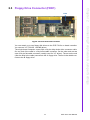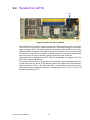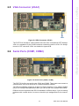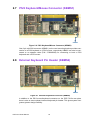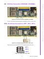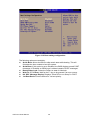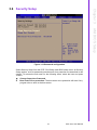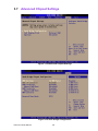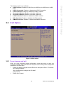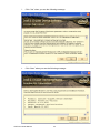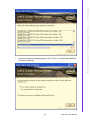
1
User Manual
PCE-7214
Dual Socket 771 Intel®
Quad-Core/Dual-Core
Xeon® Processor Card with
PCI Express / VGA /
Dual Gigabit LAN / FSB 1333 MHz
Copyright
The documentation and the software included with this product are copyrighted 2009
by Advantech Co., Ltd. All rights are reserved. Advantech Co., Ltd. reserves the right
to make improvements in the products described in this manual at any time without
notice.
No part of this manual may be reproduced, copied, translated or transmitted in any
form or by any means without the prior written permission of Advantech Co., Ltd.
Information provided in this manual is intended to be accurate and reliable. However,
Advantech Co., Ltd. assumes no responsibility for its use, nor for any infringements
of the rights of third parties, which may result from its use.
Acknowledgements
PICMG® and the PICMG® logos are trademarks of the PCI Industrial Computers
Manufacturers Group.
All other product names or trademarks are properties of their respective owners.
Certifications
CE
FCC Class A
PCE-7214 User Manual
Part No. 2002721401
Edition 2
Printed in Taiwan
May 2009
ii
A Message to the Customer
Advantech customer services
Each and every Advantech product is built to the most exacting specifications to
ensure reliable performance in the harsh and demanding conditions typical of industrial environments. Whether your new Advantech equipment is destined for the laboratory or the factory floor, you can be assured that your product will provide the
reliability and ease of operation for which the name Advantech has come to be
known.
Your satisfaction is our primary concern. Here is a guide to Advantech's customer
services. To ensure you get the full benefit of our services, please follow the instructions below carefully.
Technical support
We want you to get the maximum performance from your products. So if you run into
technical difficulties, we are here to help. For the most frequently asked questions,
you can easily find answers in your product documentation. These answers are normally a lot more detailed than the ones we can give over the phone.
So please consult this manual first. If you still cannot find the answer, gather all the
information or questions that apply to your problem, and with the product close at
hand, call your dealer. Our dealers are well trained and ready to give you the support
you need to get the most from your Advantech products. In fact, most problems
reported are minor and are able to be easily solved over the phone.
In addition, free technical support is available from Advantech engineers every business day. We are always ready to give advice on application requirements or specific
information on the installation and operation of any of our products.
iii
PCE-7214 User Manual
Product Warranty (2 years)
Advantech warrants to you, the original purchaser, that each of its products will be
free from defects in materials and workmanship for two years from the date of purchase.
This warranty does not apply to any products which have been repaired or altered by
persons other than repair personnel authorized by Advantech, or which have been
subject to misuse, abuse, accident or improper installation. Advantech assumes no
liability under the terms of this warranty as a consequence of such events.
Because of Advantech’s high quality-control standards and rigorous testing, most of
our customers never need to use our repair service. If an Advantech product is defective, it will be repaired or replaced at no charge during the warranty period. For outof-warranty repairs, you will be billed according to the cost of replacement materials,
service time and freight. Please consult your dealer for more details.
If you think you have a defective product, follow these steps:
1. Collect all the information about the problem encountered. (For example, CPU
speed, Advantech products used, other hardware and software used, etc.) Note
anything abnormal and list any onscreen messages you get when the problem
occurs.
2. Call your dealer and describe the problem. Please have your manual, product,
and any helpful information readily available.
3. If your product is diagnosed as defective, obtain an RMA (return merchandise
authorization) number from your dealer. This allows us to process your return
more quickly.
4. Carefully pack the defective product, a fully-completed Repair and Replacement
Order Card and a photocopy proof of purchase date (such as your sales receipt)
in a shippable container. A product returned without proof of the purchase date
is not eligible for warranty service.
5. Write the RMA number visibly on the outside of the package and ship it prepaid
to your dealer.
Before you begin installing your single board computer, please make sure that the
following materials have been shipped:
If any of these items are missing or damaged, contact your distributor or sales representative immediately.
We have carefully inspected the PCE-7214 mechanically and electrically before shipment. It should be free of marks and scratches and in perfect working order upon
receipt.
As you unpack the PCE-7214, check it for signs of shipping damage. (For example,
damaged box, scratches, dents, etc.) If it is damaged or it fails to meet the specifications, notify our service department or your local sales representative immediately.
Also notify the carrier. Retain the shipping carton and packing material for inspection
by the carrier. After inspection, we will make arrangements to repair or replace the
unit.
PCE-7214 User Manual
iv
Initial Inspection
Before you begin installing your single board computer, please make sure that the
following materials have been shipped:
! 1 PCE-7214 Dual Intel® Xeon® / LV Xeon® processor-based single board computer
! 1 PCE-7214 Startup Manual
! 1 CD with driver utility and manual (in PDF format)
! 1 FDD cable
P/N: 1700340640
! 2 Ultra ATA 66/100 HDD cables
P/N: 1701400452
! 2 Serial ATA HDD data cable
P/N: 1700003194
! 2 Serial ATA HDD power cable
P/N: 1703150102
! 1 Printer (parallel) port & COM port cable kit
P/N: 1701260305
! 1 Dual USB cable kit
P/N: 1700008461
! 1 Y cable for PS/2 keyboard and PS/2 mouse
P/N: 1700060202
! 1 Jumper Pack
P/N: 9689000068
! 1 User note for full-sized CPU card
! 1 Warranty card
If any of these items are missing or damaged, contact your distributor or sales representative immediately.
We have carefully inspected the PCE-7214 mechanically and electrically before shipment. It should be free of marks and scratches and in perfect working order upon
receipt.
As you unpack the PCE-7214, check it for signs of shipping damage. (For example,
damaged box, scratches, dents, etc.) If it is damaged or it fails to meet the specifications, notify our service department or your local sales representative immediately.
Also notify the carrier. Retain the shipping carton and packing material for inspection
by the carrier. After inspection, we will make arrangements to repair or replace the
unit.
Note!
Purchasing PCE-7214's proprietary CPU cooler(s) from Advantech is a
must. Other brands of CPU coolers are NOT compatible with PCE-7214.
1. Advantech P/N 1750000282: Xeon CPU Cooler for 110W TDP CPU
2. Advantech P/N 1750001660: Low Profile Xeon CPU Cooler for 55W
TDP CPU
v
PCE-7214 User Manual
Verified CPU List
CPU Family
sSpec.
Core
Power
Stepping
Vcore
FSB
Mfg. Tech HT
L2 cache
XEON-2.33 G (5148) SLABH
B2
40W
1.150V-1.250V 1333
65nm
Y
4MB
XEON-2 G (5130)
SLAGC
G0
65W
1.275V
65nm
Y
4MB
XEON-2 G (5405)
SLAP2
C0
80W
0.95V - 1.225V 1333
45nm
Y
12MB
XEON-1.60 G(5310)
SL9XR
B3
80W
1.325V max
65nm
Y
8MB
1333
1066
Verified Memory List
Brand
Transcend
RoHS)
Size
Speed
Type
ECC
Vendor PN
Memory
2GB
DDR2 533
Register DDR2
Y
TS256MQR72V5U
Micron 7WE17 D9HNL
1GB
DDR2 667
Register DDR2
Y
TS128MQR72V6J
ELPIDA E5108AG-6E-E
2GB
DDR2 667
Register DDR2
Y
TS256MQR72V6U
SAMSUNG K4T1G084QA
4GB
DDR2 667
Register DDR2
Y
TS512MQR72V6T
ELPIDA E1104AOSE-6E-E
Certification and Safety Instructions
This device complies with the requirements in part 15 of the FCC rules: Operation is
subject to the following two conditions:
1. This device may not cause harmful interference, and
2. This device must accept any interference received, including interference that
may cause undesired operation
This equipment has been tested and found to comply with the limits for a Class A digital device, pursuant to Part 15 of the FCC Rules. These limits are designed to provide reasonable protection against harmful interference when the equipment is
operated in a commercial environment. This equipment generates, uses, and can
radiate radio frequency energy and, if not installed and used in accordance with the
instruction manual, may cause harmful interference to radio communications. Operation of this device in a residential area is likely to cause harmful interference in which
case the user will be required to correct the interference at his/her own expense. The
user is advised that any equipment changes or modifications not expressly approved
by the party responsible for compliance would void the compliance to FCC regulations and therefore, the user's authority to operate the equipment.
Caution! There is a danger of a new battery exploding if it is incorrectly installed.
Do not attempt to recharge, force open, or heat the battery. Replace the
battery only with the same or equivalent type recommended by the manufacturer. Discard used batteries according to the manufacturer's
instructions.
PCE-7214 User Manual
vi
Contents
Chapter
1
Hardware Configuration......................1
1.1
1.2
1.3
Introduction ............................................................................................... 2
Features .................................................................................................... 3
Specifications ............................................................................................ 3
1.3.1 System .......................................................................................... 3
1.3.2 Memory ......................................................................................... 3
1.3.3 Input/Output .................................................................................. 4
1.3.4 Graphic interface........................................................................... 4
1.3.5 Ethernet LAN ................................................................................ 4
1.3.6 Industrial features ......................................................................... 4
1.3.7 Mechanical and environmental specifications............................... 4
Jumpers and Connectors .......................................................................... 5
Table 1.1: Jumper descriptions ................................................... 5
Table 1.2: Connector descriptions............................................... 5
Board Layout: Jumper and Connector Locations...................................... 6
Figure 1.1 Jumper and Connector locations................................ 6
PCE-7214 Block Diagram ......................................................................... 7
Figure 1.2 Block Diagram ............................................................ 7
Safety Precautions .................................................................................... 8
System Memory ........................................................................................ 8
Memory Installation Procedures................................................................ 8
Processor Installation................................................................................ 9
CPU Cooler Installation........................................................................... 10
Figure 1.3 CPU Cooler Installation ............................................ 10
1.4
1.5
1.6
1.7
1.8
1.9
1.10
1.11
Chapter
2
Connecting Peripherals & Jumper
Settings ..............................................11
2.1
2.2
Introduction ............................................................................................. 12
IDE Connector (IDE1) ............................................................................. 12
Figure 2.1 PCE-7214 IDE1 location........................................... 12
Floppy Drive Connector (FDD1).............................................................. 13
Figure 2.2 PCE-7214 FDD1 location ......................................... 13
Parallel Port (LPT1)................................................................................. 14
Figure 2.3 PCE-7214 LPT1 location .......................................... 14
VGA Connector (VGA1) .......................................................................... 15
Figure 2.4 VGA Connector (VGA1) ........................................... 15
Serial Ports (COM1, COM2) ................................................................... 15
Figure 2.5 Serial Ports (COM1, COM2)..................................... 15
PS/2 Keyboard/Mouse Connector (KBMS1) ........................................... 16
Figure 2.6 PS/2 Keyboard/Mouse Connector (KBMS1) ........... 16
External Keyboard Pin Header (KBMS2) ................................................ 16
Figure 2.7 External Keyboard Connector (KBMS2).................. 16
CPU Fan Connectors (CPUFAN1, CPUFAN2) ....................................... 17
Figure 2.8 CPU Fan Connectors (CPUFAN1, CPUFAN2) ....... 17
Front Panel Connectors (JFP1, JFP2, JFP3)......................................... 17
Figure 2.9 Front Panel Connectors (JFP1, JFP2, JFP3) .......... 17
Figure 2.10 Detail (JFP1, JFP2, JFP3)....................................... 17
2.10.1 ATX soft power switch (JFP1 / PWR_SW) ................................. 18
2.10.2 2.12.2 Reset (JFP1 / RESET)..................................................... 18
2.10.3 HDD LED (JFP2 / HDDLED)....................................................... 18
2.10.4 SM Bus Connector (JFP2 / SNMP)............................................. 18
2.10.5 External speaker (JFP2 / SPEAKER) ......................................... 18
2.3
2.4
2.5
2.6
2.7
2.8
2.9
2.10
vii
PCE-7214 User Manual
2.11
2.12
2.13
2.14
2.15
2.16
2.17
Chapter
3
3.1
3.2
3.3
3.4
3.5
3.6
3.7
3.8
PCE-7214 User Manual
2.10.6 Power LED and keyboard lock connector (JFP3 / PWR_LED&KEY
LOCK)......................................................................................... 18
Table 2.1: ATX power supply LED status (No support for AT power) ............................................................................. 18
HW Monitor Alarm (JOBS1) / Watch Dog Timer (JWDT1) / Infrared (JIR1)
................................................................................................................ 19
Figure 2.11HW Monitor Alarm (JOBS1) ..................................... 19
2.11.1 HW Monitor Alarm (JOBS1)........................................................ 19
Table 2.2: Hardware Monitor Alarm setting............................... 19
2.11.2 Watchdog timer output (JWDT1) ................................................ 19
Table 2.3: Watchdog timer output (JWDT1).............................. 19
2.11.3 Infrared Connector (JIR1) ........................................................... 19
Dual Giga LAN RJ45 connector (LAN12) ............................................... 20
Figure 2.12Dual Giga LAN RJ45 connector (LAN12)................. 20
High Definition Audio Interface (HDAUD1) ............................................. 20
Figure 2.13High Definition Audio Interface (HDAUD1)............... 20
Serial ATA interface (SATA1 ~ SATA6).................................................. 21
Figure 2.14Serial ATA interface (SATA1 ~ SATA6) ................... 21
LAN1 and LAN2 LED connector (LANLED1).......................................... 21
Figure 2.15LAN1 and LAN2 LED connector (LANLED1) ........... 21
GPIO header (GPIO1) ............................................................................ 22
Figure 2.16 GPIO header (GPIO1)............................................. 22
CMOS clear (CMOS1) ............................................................................ 22
Table 2.4: CMOS (CMOS1) ...................................................... 22
AMI BIOS Setup................................. 23
Figure 3.1 Setup program initial screen..................................... 24
Entering Setup ........................................................................................ 25
Main Setup.............................................................................................. 25
Figure 3.2 Main setup screen .................................................... 25
3.2.1 System time / System date ......................................................... 25
Advanced BIOS Features Setup............................................................. 26
Figure 3.3 Advanced BIOS features setup screen .................... 26
3.3.1 CPU configuration....................................................................... 27
Figure 3.4 CPU configuration setting......................................... 27
3.3.2 IDE configuration ........................................................................ 28
Figure 3.5 IDE configuration...................................................... 28
3.3.3 Super I/O configuration............................................................... 29
Figure 3.6 Super I/O configuration ............................................ 29
3.3.4 Hardware health function............................................................ 30
Figure 3.7 Hardware health configuration. ................................ 30
3.3.5 APM configuration ...................................................................... 31
Figure 3.8 APM configuration .................................................... 31
Figure 3.9 Configure remote access type and parameters ....... 32
PCI/PNP Setup ....................................................................................... 33
Figure 3.10PCI/PNP setup ......................................................... 33
Boot Setup Utility .................................................................................... 35
Figure 3.11Boot setup utility ....................................................... 35
Figure 3.12Boot setting configuration......................................... 36
Security Setup......................................................................................... 37
Figure 3.13Password configuration ............................................ 37
Advanced Chipset Settings..................................................................... 38
Figure 3.14Advanced Chipset Settings ...................................... 38
Figure 3.15Souh bridge configuration ........................................ 38
Exit Option .............................................................................................. 39
Figure 3.16Exit option................................................................. 39
3.8.1 Save changes and exit ............................................................... 39
3.8.2 Discard changes and exit ........................................................... 40
viii
3.8.3
3.8.4
Chapter
Load optimal defaults.................................................................. 40
Load fail-Safe defaults ................................................................ 40
4
Chipset Software Installation Utility 41
4.1
4.2
4.3
Before you Begin..................................................................................... 42
Introduction ............................................................................................. 42
Driver Setup ............................................................................................ 43
5
Graphic Setup ....................................47
5.1
5.2
Introduction ............................................................................................. 48
Windows XP Driver Setup....................................................................... 48
6
LAN Configuration.............................49
6.1
6.2
6.3
6.4
Introduction ............................................................................................. 50
Features .................................................................................................. 50
Installation ............................................................................................... 50
Win XP Driver Setup (LAN)..................................................................... 51
7
SATA RAID Setup ..............................55
7.1
7.2
Introduction ............................................................................................. 56
SATA RAID Driver and Utility Setup ....................................................... 56
Appendix A
Programming the Watchdog Timer..57
A.1
Watchdog Timer...................................................................................... 58
A.1.1 Watchdog timer overview............................................................ 58
A.1.2 Reset/ Interrupt selection ............................................................ 58
A.1.3 Programming the Watchdog Timer ............................................. 58
Table A.1: Watchdog Timer Registers ....................................... 60
A.1.4 Example Program ....................................................................... 61
Appendix B
I/O Pin Assignments..........................65
B.1
IDE Hard Drive Connector (IDE1) ........................................................... 66
Table B.1: IDE hard drive connector (IDE1) .............................. 66
Floppy Drive Connector (FDD1).............................................................. 67
Table B.2: Floppy drive connector (FDD1) ................................ 67
Parallel Port Connector (LPT1) ............................................................... 68
Table B.3: Parallel port connector (LPT1).................................. 68
VGA Connector (VGA1) .......................................................................... 68
Table B.4: VGA connector (VGA1) ............................................ 68
RS-232 Serial Port (COM1,COM2) ......................................................... 69
Table B.5: RS-232 serial port (COM1,COM2) ........................... 69
PS/2 Keyboard/Mouse Connector (KBMS1) ........................................... 69
Table B.6: PS/2 keyboard/mouse connector (KBMS1).............. 69
External Keyboard/Mouse Pin Header (KBMS2) .................................... 70
Table B.7: External Keyboard/Mouse Pin Header (KBMS2....... 70
CPU Fan Power Connector (CPUFAN1,CPUFAN2)............................... 70
Table B.8: CPU Fan Power Connector (CPUFAN1,CPUFAN2) 70
Power LED and Keyboard Lock Connector
(JFP3 / PWR_LED & KEY
LOCK) ..................................................................................................... 70
Chapter
Chapter
Chapter
B.2
B.3
B.4
B.5
B.6
B.7
B.8
B.9
ix
PCE-7214 User Manual
B.10
B.11
B.12
B.13
B.14
B.15
B.16
B.17
B.18
B.19
B.20
B.21
B.22
Table B.9: Power LED and Keyboard Lock Connector (JFP3 /
PWR_LED & KEY LOCK) ........................................ 70
External Speaker Connector (JFP2 / SPEAKER) ................................... 71
Table B.10:External Speaker Connector (JFP2 / SPEAKER) .... 71
Reset Connector (JFP1 / RESET) .......................................................... 71
Table B.11:Reset connector (JFP1 / RESET) ............................ 71
HDD LED (JFP2 / HDDLED)................................................................... 71
Table B.12:Reset connector (JFP1 / RESET) ............................ 71
ATX Soft Power Switch (JFP1 / PWR_SW)............................................ 72
Table B.13:Reset connector (JFP1 / RESET) ............................ 72
Hi-definition audio Link connector (HDAUD1)......................................... 72
Table B.14:Hi-definition audio link connector (HDAUD1) ........... 72
SM Bus Connector (JFP2 / SNMP)......................................................... 72
Table B.15:SM bus connector (JFP2 / SNMP) ........................... 72
LAN1 and LAN2 LED connector (LANLED1).......................................... 73
Table B.16:LAN1 and LAN2 LED connector (LANLED1) ........... 73
GPIO header (GPIO1) ............................................................................ 73
Table B.17:GPIO header (GPIO1).............................................. 73
System I/O Ports..................................................................................... 74
Table B.18:System I/O ports....................................................... 74
DMA Channel Assignments .................................................................... 75
Table B.19:DMA channel assignments....................................... 75
Interrupt Assignments ............................................................................. 75
Table B.20:Interrupt assignments............................................... 75
1st MB Memory Map............................................................................... 75
Table B.21:1st MB memory map ................................................ 75
PCI Bus Map........................................................................................... 76
Table B.22:PCI bus map............................................................. 76
Appendix C
Programming the GPIO and Watchdog
Timer .................................................. 77
C.1
Supported GPIO Register ....................................................................... 78
C.1.1 GPIO Registers........................................................................... 78
C.1.2 GPIO Example program-1 .......................................................... 79
PCE-7214 User Manual
x
Chapter
1
Hardware
Configuration
1
1.1 Introduction
PCE-7214 is a server-grade PICMG® 1.3 full-sized system host board (SHB) that
features dual Intel® Quad/Dual-Core Xeon computing power. It is an ideal solution for
industrial HPC (high-performance PC) applications such as medical image processing, environment monitoring and telecommunications.
PCE-7214 is designed with an Intel® E5100 server chipset and has two LGA771
sockets for supporting dual Intel® Quad-Core or Dual-Core Xeon processors with
1333 MHz FSB and DDR2 667 MHz ECC and registered SDRAM up to 32 GB. High
computing power makes it suitable for today’s industrial applications that need
intense image or data processing.
The PCIe lanes from PCE-7214 north bridge can be flexibly configured as PCIe x16,
x 8 or x4 ports, plus four PCIe x 1 lanes from the south bridge, the PCE-7214 can be
used with all Advantech PCE-5000 and PCE-7000 series backplanes for utilizing
PCIe x16, x8, x4 and x 1 add-on cards. With supporting 30 Advantech backplanes,
the PCI, PCI-X, and PCIe expansion options are both robust and numerous.
PCE-7214 is rich in I/O interfaces: it has six SATA 2 ports with RAID 0, 1, 5, and 10,
providing high data transmission rates (300 MB/sec) and super-reliable read/write
performance. The two serial ports (COM ports) can be used for device control applications. Dual Gigabit Ethernet LANs offer strong networking capability.
PCE-7214 has a PCIe x 1 interface XGI Volari Z11 graphics controller with 64 MB
independent frame buffer memory, featuring low power and fan less on-board graphic
solution, PCE-7214 provides targeted performance and reliable graphic capability for
industrial server application.
In addition to board-level products, Advantech also offers rack-mount and wall-mount
chassis options; with PCE-7214 joining the product portfolio, Advantech now can provide whole new high performance system-level solutions for industrial customers.
With outstanding performance and flexible expansion capability, PCE-7214 is an
ideal computing platform for modern industrial HPC applications.
PCE-7214 User Manual
2
Compliance with PICMG® 1.3
!
Support single/dual LGA771 socket Intel® Xeon® / LV Xeon® FSB 1333 Mhz
processors
Support Dual Channel DDR2 533/667 ECC Registered SDRAM up to 32 GB
Two PCI Express X 8 or one x 16, and One X4 to backplane (Compatible with
Advantech PCE-7000 and PCE-5000 series backplanes)
4 PCI 32bits / 33 MHz masters to backplane
!
!
!
!
!
!
!
!
!
Intel® 82566DM/82573V Dual Gigabit Ethernet via dedicated PCI Express X1
port
Onboard XGI® Volari® Z11 with 64 MB frame buffer memory
6 SATA HDDs Support S/W SATA RAID 0, 1, 5, 10
8 USB 2.0 ports on CPU card and 4 ones on backplane
Remote management with SNMP-1000-B1 modules
CMOS automatic back and prevent accidental data loss of BIOS setup
1.3 Specifications
1.3.1 System
!
!
!
CPU: Dual Intel® 1333 MHz Quad-Core / Dual-Core Xeon® or LV Xeon® processors
L2 Cache: CPU built-in 12 MB / 6 MB L2 cache
BIOS: AMI Flash BIOS (32 Mb Flash Memory)
!
!
System Chipset: Intel® E5100 + ICH9R
SATA/EIDE hard disk drive interface: Supports up to 6 independent Serial
ATA hard drives (up to 300 MB/s) with software RAID 0, 1, 5, 10 as well as one
IDE port (maximum 2 devices)
!
Floppy disk drive interface: Supports up to two floppy disk drives, 51/4 (360
KB and 1.2 MB) and/or 31/2 (720 KB, 1.44 MB). BIOS enabled/disabled.
1.3.2 Memory
!
RAM: Up to 32 GB in four 240-pin DIMM sockets. Supports Dual-channel DDR2
533/667 MHz (ECC Registered DIMM).
Note!
PCE-7214 is NOT compatible with DDR2 memory modules that DO
NOT have ECC and register functions. I.E., DDR2 memory modules
MUST have ECC and register functions.
3
PCE-7214 User Manual
Hardware Configuration
!
Chapter 1
1.2 Features
1.3.3 Input/Output
!
!
!
!
!
!
!
!
Bus interface: PICMG® 1.3 SHB Express compliant bus interface
PCI Express Bus: Two x8 / one x 16 & one x4 to backplane
PCI Bus: Four 32bit / 33 MHz PCI masters to backplane
Enhanced parallel port: Configurable to LPT1, LPT2, LPT3, or disabled. Standard DB-25 female connector provided. Supports EPP/SPP/ECP
Serial ports: Two RS-232 ports
Keyboard and PS/2 mouse connector: One 6-pin mini-DIN connector is
located on the mounting bracket for easy connection to a keyboard or PS/2
mouse. An on board keyboard pin header connector is also available
High Definition Audio: PCE-7214 can provide audio function with the optional
audio extension module PCA-AUDIO-HDA1E
USB ports: PCE-7214 supports up to 12 USB 2.0 ports with transmission rates
up to 480Mbps; 8 USB ports on the CPU card, 4 USB ports on the backplane.
1.3.4 Graphic interface
!
!
!
Controller: XGI Volari Z11
VRAM: 64 MB frame buffer memory on chip
Resolution: 1600 x 1200 at 70 Hz VGA output;15 pin D-Sub connector x1
1.3.5 Ethernet LAN
!
Supports dual10/100/1000 Mbps Ethernet networking
!
Controller: LAN 1: Intel® 82566DM; LAN 2: Intel® 82573V
1.3.6 Industrial features
!
Watchdog timer: Can generate a system reset. The watchdog timer is programmable, with each unit equal to one second or one minute (255 levels). You
can find programming detail in Appendix A
1.3.7 Mechanical and environmental specifications
!
!
!
!
!
Operating temperature: 0 ~ 60° C (32 ~ 140° F, depending on CPU)
Storage temperature: -20 ~ 70° C (-4 ~ 158° F)
Humidity: 20 ~ 95% non-condensing
Power supply voltage: +5 V, + 12 V, 3.3 V, +5 VSBY
Power consumption:
CPU:Two Intel® Xeon® 2.0 GHz / 4M/ 1333 MHz FSB / 65W TDP
MEMORY: DDR2 2GB *4
!
!
Test program, Intel® Max power 100% + BurnIn test 4.0
+12 V
9.7 A
+5 V
7.4 A
+3.3 V
2.5 A
+5 VSB
0.71 A
-12 V
0A
-5 V
0A
Board size: 338 x 122 mm (13.3 x 4.8 inch)
Board weight: 0.5 kg (1.2 lb)
PCE-7214 User Manual
4
Connectors on the PCE-7214 single board computer link it to external devices such
as hard disk drives and a keyboard. In addition, the board has a number of jumpers
used to configure your system for your application.
Below, Table 1.1 and Table 1.2 list the jumper and connector functions. Later sections
in this chapter give instructions on setting jumpers. Chapter 2 gives instructions for
connecting external devices to your single board computer.
Chapter 1
1.4 Jumpers and Connectors
Table 1.1: Jumper descriptions
Function
CMOS1
CMOS Clear
JWDT1
Watchdog timer output option
Hardware Configuration
Label
Table 1.2: Connector descriptions
Label
Function
IDE1
Primary IDE connector
FDD1
Floppy drive connector
LPT1
Parallel port
VGA1
VGA connector
COM1
Serial port:COM1 (9-pin connector)
COM2
Serial port:COM2 (9-pin connector)
KBMS1
PS/2 keyboard and mouse connector
KBMS2
External keyboard/mouse pin header
JIR1
Infrared port pin header
CPUFAN1
CPU1 FAN connector
CPUFAN2
CPU2 FAN connector
JFP1
Power and Reset Button connector
JFP2
HDD LED / SNMP(SM bus) / Speaker connector
JFP3
Power LED and keyboard lock connector
JOBS1
HW Monitor Alarm
Close: Enable OBS Alarm
Open: Disable OBS Alarm
LAN12
Dual Giga LAN RJ45 connector with Transformer
HDAUD1
AC'97 Link connector
SATA1
Serial ATA1
SATA2
Serial ATA2
SATA3
Serial ATA3
SATA4
Serial ATA4
SATA5
Serial ATA5
SATA6
Serial ATA6
USB 12
USB port 1 and port 2
USB 34
USB port 3 and port 4
USB 56
USB port 5 and port 6
USB 78
USB port 7 and port 8
LANLED1
LAN1 and LAN2 LED connector
GPIO1
GPIO header
5
PCE-7214 User Manual
1.5 Board Layout: Jumper and Connector
Locations
DIMMA2 DIMMB2
CPUFAN1
DIMMA1 DIMMB1
CPUFAN2
USB56
HDAUD1
USB78
1
USB12
3
SATA 1~4
2
6
SATA 5~6
5
USB34
4
GPIO1
JOBS1
IDE1
FDD1
COM1
LPT1
LANLED1
COM2
LAN12
VGA1
KBMS1
KBMS2
6
PCE-7214 User Manual
CPU2
CPU1
JWDT1
JIR1
Figure 1.1 Jumper and Connector locations
Chapter 1
1.6 PCE-7214 Block Diagram
Hardware Configuration
Figure 1.2 Block Diagram
7
PCE-7214 User Manual
1.7 Safety Precautions
Warning! Always completely disconnect the power cord from your chassis whenever you work with the hardware. Do not make connections while the
power is on. Sensitive electronic components can be damaged by sudden power surges. Only experienced electronics personnel should open
the PC chassis.
Caution! Always ground yourself to remove any static charge before touching the
single board computer. Modern electronic devices are very sensitive to
static electric discharges. As a safety precaution, use a grounding wrist
strap at all times. Place all electronic components on a static-dissipative
surface or in a static-shielded bag when they are not in the chassis.
Caution! The computer is provided with a battery-powered Real-time Clock circuit. There is a danger of explosion if battery is incorrectly replaced.
Replace only with same or equivalent type recommended by the manufacturer. Discard used batteries according to manufacturer's instructions.
Note!
Before install your PCE-7214 into a chassis, make sure that all components on both sides of the CPU card do not touch any metal parts, especially the chassis wall and add-on card at the adjacent slot.
1.8 System Memory
The PCE-7214 has four sockets for 240-pin dual inline memory modules (DIMMs) in
two separated memory channels. It can operate with single channel or dual channel
modules. We recommend using dual channel mode to provide optimized performance. All these sockets use ECC registered DDR2-533/667 SDRAM. The maximum memory size is up to 32 GB.
1.9 Memory Installation Procedures
To install DIMMs, first make sure the two handles of the DIMM socket are in the
“open” position. i.e. The handles lean outward. Slowly slide the DIMM module along
the plastic guides on both ends of the socket. Then press the DIMM module right
down into the socket, until you hear a click. This is when the two handles have automatically locked the memory module into the correct position of the DIMM socket. To
remove the memory module, just push both handles outward, and the memory module will be ejected by the mechanism in the socket.
PCE-7214 User Manual
8
The CPU on the board must have a fan and heat sink attached, to prevent overheating.
Note!
Owing to a limitation of the Intel® E5100 chipset, when you only use single CPU on the PCE-7214, the CPU has to be installed in the CPU1
socket. Otherwise the system cannot boot up normally.
1.
2.
3.
4.
Make sure the socket LGA771 lever is in the upright position. To raise the lever,
pull it out to the side a little and raise it as far as it will go.
Place the CPU in the empty socket. Follow the instructions that came with the
CPU. If you have no instructions, complete the following procedure. Carefully
align the CPU so it is parallel to the socket and the notches on the corners of the
CPU correspond with the notches on the inside of the socket. Gently slide the
CPU in. It should insert easily. If it does not insert easily, pull the lever up a little
bit more.
Press the lever down. The plate will slide forward. You will feel some resistance
as the pressure starts to secure the CPU in the socket. This is normal and will
not damage the CPU. When the CPU is installed, the lever should snap into
place at the side of the socket.
PCE-7214 accessory includes two CPU heat sink, please follow the installation
guide in the heat sink Box to install it properly.CP
9
PCE-7214 User Manual
Hardware Configuration
Warning! Without a fan or heat sink, the CPU will over-heat and cause damage to
both the CPU and the single board computer. To install a CPU, first turn
off your system and remove its cover.
Chapter 1
1.10 Processor Installation
1.11 CPU Cooler Installation
Please ensure that the CPU cooler included with the PCE-7214 is installed as follows:
Note!
Purchasing PCE-7214's proprietary CPU cooler(s) from Advantech is a
must. Other brands of CPU coolers are NOT compatible with PCE-7214.
1. Advantech P/N 1750000282: Xeon CPU Cooler for 110W TDP CPU
2. Advantech P/N 1750001660: Low Profile Xeon CPU Cooler for 55W
TDP CPU
Figure 1.3 CPU Cooler Installation
PCE-7214 User Manual
10
Chapter
2
2
Connecting
Peripherals & Jumper
Settings
2.1 Introduction
You can access most of the connectors from the top of the board while it is installed
in the chassis. If you have a number of cards installed or have a packed chassis, you
may need to partially remove the card to make all the connections.
You can configure your single board computer to match the needs of your application
by setting the jumpers. A jumper is a metal bridge that closes an electrical circuit. It
consists of two metal pins and a small metal clip (often protected by a plastic cover)
that slides over the pins to connect them. To "close" (or turn ON) a jumper, you connect the pins with the clip. To "open" (or turn OFF) a jumper, you remove the clip.
Sometimes a jumper consists of a set of three pins, labeled 1, 2, and 3. In this case,
you connect either pins 1 and 2, or 2 and 3. A pair of needle-nose pliers may be useful when setting jumpers.
2.2 IDE Connector (IDE1)
IDE1
Figure 2.1 PCE-7214 IDE1 location
You can attach up to two IDE (Integrated Drive Electronics) drives to the PCE-7214's
built-in controller. The primary connector can accommodate two drives.
Wire number 1 on the cable is red or blue and the other wires are gray. Connect one
end to connector IDE1 on the single board computer. Make sure that the red/blue
wire corresponds to pin 1 on the connector (in the upper right hand corner). See
Chapter 1 for help finding the connector.
Unlike floppy drives, IDE hard drives can connect in either position on the cable. If
you install two drives to a single connector, you will need to set one as the master
and the other as the slave. You do this by setting the jumpers on the drives. If you
use just one drive per connector, you should set each drive as the master. See the
documentation that came with your drive for more information.
Connect the first hard drive to the other end of the cable. Wire 1 on the cable should
also connect to pin 1 on the hard drive connector, which is labeled on the drive circuit
board. Check the documentation that came with the drive for more information.
PCE-7214 User Manual
12
FDD1
You can attach up to two floppy disk drives to the PCE-7214's on board controller.
You can use 3.5" (720 KB, 1.44 MB) drives.
The single board computer comes with a 34-pin daisy-chain drive connector cable.
On one end of the cable is a 34-pin flat-cable connector. On the other end are two
sets of 34-pin flat-cable connector (usually used for 3.5" drives). The set on the end
(after the twist in the cable) connects to the A: floppy drive. The set in the middle connects to the B: floppy drive.
13
PCE-7214 User Manual
Connecting Peripherals & Jumper Settings
Figure 2.2 PCE-7214 FDD1 location
Chapter 2
2.3 Floppy Drive Connector (FDD1)
2.4 Parallel Port (LPT1)
LPT1
Figure 2.3 PCE-7214 LPT1 location
The parallel port is normally used to connect the single board computer to a printer.
The PCE-7214 includes an onboard parallel port, accessed through a 26-pin flatcable connector, LPT1. The card comes with an adapter cable which lets you use a
traditional DB-25 connector. The cable has a 26-pin connector on one end and a DB25 connector on the other, mounted on a retaining bracket. The bracket installs at the
end of an empty slot in your chassis, giving you access to the connector.
The parallel port is designated as LPT1, and can be disabled or changed to LPT2 or
LPT3 in the system BIOS setup.
To install the bracket, find an empty slot in your chassis. Unscrew the plate that covers the end of the slot. Screw in the bracket in place of the plate. Next, attach the flatcable connector to LPT1 on the CPU card. Wire 1 of the cable is red or blue, and the
other wires are gray. Make sure that wire 1 corresponds to pin 1 of LPT1. Pin 1 is on
the upper right side of LPT1.
PCE-7214 User Manual
14
Chapter 2
2.5 VGA Connector (VGA1)
Figure 2.4 VGA Connector (VGA1)
The PCE-7214 includes a VGA interface that can drive conventional CRT displays.
VGA1 is a standard 15-pin D-SUB connector commonly used for VGA. Pin assignments for CRT connector VGA1 are detailed in Appendix B.
2.6 Serial Ports (COM1, COM2)
COM2 COM1
Figure 2.5 Serial Ports (COM1, COM2)
The PCE-7214 offers two serial ports COM1 and COM2. These ports can connect to
serial devices, such as a mouse or to a communications network.
The IRQ and address ranges for all ports are fixed. However, if you want to disable
the port or change these parameters later, you can do this in the system BIOS setup.
Different devices implement the RS-232 standard in different ways. If you are having
problems with a serial device, be sure to check the pin assignments for the connector.
15
PCE-7214 User Manual
Connecting Peripherals & Jumper Settings
VGA1
2.7 PS/2 Keyboard/Mouse Connector (KBMS1)
KBMS1
Figure 2.6 PS/2 Keyboard/Mouse Connector (KBMS1)
One 6-pin mini-DIN connector (KBMS1) on the card mounting bracket provides connection to a PS/2 keyboard or a PS/2 mouse, respectively. KBMS1 can also be connected to an adapter cable (P/N: 1700060202) for connecting to both a PS/2
keyboard and a PS/2 mouse.
2.8 External Keyboard Pin Header (KBMS2)
KBMS2
Figure 2.7 External Keyboard Connector (KBMS2)
In addition to the PS/2 mouse/keyboard connector on the PCE-7214's rear plate,
there is also an extra onboard external keyboard pin header. This gives system integrators greater design flexibility.
PCE-7214 User Manual
16
Figure 2.8 CPU Fan Connectors (CPUFAN1, CPUFAN2)
If a fan is used, these connectors support cooling fans of 12V/1A (12W) or less.
2.10 Front Panel Connectors (JFP1, JFP2, JFP3)
Page JFPX Figure 2.9 Front Panel Connectors (JFP1, JFP2, JFP3)
There are several external switches to monitor and control the PCE-7214.
PWR_SW
RESET
HDDLED
SNMP
SPEAKER
PWR_LED&KEY LOCK
JFP1
JFP2
JFP3
Figure 2.10 Detail (JFP1, JFP2, JFP3)
17
PCE-7214 User Manual
Connecting Peripherals & Jumper Settings
CPUFAN2 CPUFAN1
Chapter 2
2.9 CPU Fan Connectors (CPUFAN1, CPUFAN2)
2.10.1 ATX soft power switch (JFP1 / PWR_SW)
If your computer case is equipped with an ATX power supply, you should connect the
power on/off button on your computer case to (JFP1 / PWR_SW). This connection
enables you to turn your computer on and off.
2.10.2 2.12.2 Reset (JFP1 / RESET)
Many computer cases offer the convenience of a reset button. Connect the wire for the reset button.
2.10.3 HDD LED (JFP2 / HDDLED)
You can connect an LED to connector (JFP2 / HDDLED) to indicate when the HDD is
active.
2.10.4 SM Bus Connector (JFP2 / SNMP)
This connector is reserved for Advantech's SNMP-1000 HTTP/SNMP Remote System Manager. The SNMP-1000 allows users to monitor the internal voltages, temperature and fans from a remote computer through an Ethernet network.
(JFP2 / SNMP) can be connected to CN19 of SNMP-1000. Please be careful about
the pin assignments, pin 1 must be connected to pin 1 and pin 2 to pin 2 on both ends
of cable.
2.10.5 External speaker (JFP2 / SPEAKER)
(JFP2 / SPEAKER) is a 4-pin connector for an external speaker. If there is no external speaker, the PCE-7214 provides an onboard buzzer as an alternative. To enable
the buzzer, set pins 3-4 as closed.
2.10.6 Power LED and keyboard lock connector (JFP3 /
PWR_LED&KEY LOCK)
(JFP3 / PWR_LED&KEY LOCK) is a 5-pin connector for the power on LED and Key
Lock function. Refer to Appendix B for detailed information on the pin assignments.
The Power LED cable should be connected to pin 1-3. The key lock button cable
should be connected to pin 4-5. There are 3 modes for the power supply connection.
The first is "ATX power mode", system is on/off by a tentative power button. The second is "AT Power Mode", system is on/off by the switch of the Power supply. The third
is another "AT Power Mode" which is using the front panel power switch. The power
LED status is indicated as following table:
Table 2.1: ATX power supply LED status (No support for AT power)
Power mode
LED (ATX Power mode) LED (AT Power mode) LED (AT Power
(On/off by tentative
(On/off by switch of
mode) (On/off by
button)
Power supply)
front panel Switch)
PSON1
(On Back-plane
Jumper setting)
2-3 pin closed
1-2 pin closed
Connect 1-2 pin
cable with switch
System On
On
On
On
System Suspend
Fast flashes
Fast flashes
Fast flashes
System Off
Slow flashes
Off
Off
PCE-7214 User Manual
18
JOBS1
Page MISCX JIR1
Figure 2.11 HW Monitor Alarm (JOBS1)
2.11.1 HW Monitor Alarm (JOBS1)
(JOBS1) is a 2-pin connector for setting enable/disable alarm while the On Board
security event acts.
Table 2.2: Hardware Monitor Alarm setting
Pin setting
Function
Close
Enable OBS alarm
open
Disable OBS alarm
2.11.2 Watchdog timer output (JWDT1)
The PCE-7214 contains a watchdog timer that will reset the CPU in the event the
CPU stops processing. This feature means the PCE-7214 will recover from a software failure or an EMI problem. The JWDT1 jumper settings control the outcome of
what the computer will do in the event the watchdog timer is tripped.
Table 2.3: Watchdog timer output (JWDT1)
Function
Enable
* Disable
Jumper Setting
1
2
3
1
2
3
1 - 2 closed
2 - 3 closed
* default setting
2.11.3 Infrared Connector (JIR1)
This 5-pin header is for connecting infrared device connector.
19
PCE-7214 User Manual
Connecting Peripherals & Jumper Settings
JWDT1
Chapter 2
2.11 HW Monitor Alarm (JOBS1) / Watch Dog Timer
(JWDT1) / Infrared (JIR1)
2.12 Dual Giga LAN RJ45 connector (LAN12)
LAN12
Figure 2.12 Dual Giga LAN RJ45 connector (LAN12)
PCE-7214 uses the Intel® 82566DM/82573V Gigabit LAN chips are linked to dedicated PCIe x1 lanes. PCE-7214 provide high throughputs for heavy loading networking environment. It provides two RJ-45 connectors in the rear side and is convenient
for most industrial applications.
2.13 High Definition Audio Interface (HDAUD1)
HDAUD1
Figure 2.13 High Definition Audio Interface (HDAUD1)
The PCE-7214 provides high definition audio through PCA-AUDIO-HDA1E module
from Advantech.
PCE-7214 User Manual
20
SATA 1~6
1
5
2
3
4
6
In addition to the EIDE interface (up to two devices), the PCE-7214 features a high
performance serial ATA interfaces (up to 300 MB/s) that eases cabling to hard drives
with thin and long cables. These six port can be configured as RAID 0, 1, 5, 10
modes.
2.15 LAN1 and LAN2 LED connector (LANLED1)
LANLED1
Figure 2.15 LAN1 and LAN2 LED connector (LANLED1)
PCE-7214 provides an external LAN LED Pin header for connecting to the front side
of the chassis. With this convenient design users may know whether the LAN port is
acting or not easily. Refer to Appendix B for detailed information on the pin assignments.
PCE-7214 User Manual
Connecting Peripherals & Jumper Settings
Figure 2.14 Serial ATA interface (SATA1 ~ SATA6)
21
Chapter 2
2.14 Serial ATA interface (SATA1 ~ SATA6)
2.16 GPIO header (GPIO1)
GPIO1
Figure 2.16 GPIO header (GPIO1)
PCE-7214 provides 14-Pins pin header for Digital I/O usage. Refer to Appendix B for
detailed information on the pin assignments and programming guide in Appendix B.
2.17 CMOS clear (CMOS1)
The PCE-7214 single board computer contains a jumper that can erase CMOS data
and reset the system BIOS information. Normally this jumper should be set with pins
1-2 closed. If you want to reset the CMOS data, set CMOS1 to 2-3 closed for just a
few seconds, and then move the jumper back to 1-2 closed. This procedure will reset
the CMOS to its default setting.
Table 2.4: CMOS (CMOS1)
Function
* Keep CMOS data
Clear CMOS data
Jumper Setting
1
2
3
1
2
3
1 - 2 closed
2 - 3 short
* default setting
CMOS1
PCE-7214 User Manual
22
Chapter
3
AMI BIOS Setup
3
AMI BIOS has been integrated into many motherboards for over a decade. In the
past, people often referred to the AMI BIOS setup menu as BIOS, BIOS setup or
CMOS setup.
With the AMI BIOS Setup program, you can modify BIOS settings and control the
special features of your computer. The Setup program uses a number of menus for
making changes and turning the special features on or off. This chapter describes the
basic navigation of the PCE-7214 setup screens.
Figure 3.1 Setup program initial screen
AMI's BIOS ROM has a built-in Setup program that allows users to modify the basic
system configuration. This type of information is stored in battery-backed up CMOS
so it retains the Setup information when the power is turned off.
PCE-7214 User Manual
24
Press the "Del" key during the Power On Self Test (POST) process and you can
enter the BIOS setup screen, otherwise the system will continue the POST process.
3.2 Main Setup
Figure 3.2 Main setup screen
The Main BIOS setup screen has two main frames. The left frame displays all the
options that can be configured. Grayed-out options cannot be configured; options in
blue can. The right frame displays the key legend.
Above the key legend is an area reserved for a text message. When an option is
selected in the left frame, it is highlighted in white. Often a text message will accompany it.
3.2.1 System time / System date
Use this option to change the system time and date. Highlight System Time or System Date using the <Arrow> keys. Enter new values through the keyboard. Press the
<Tab> key or the <Arrow> keys to move between fields. The date must be entered in
MM/DD/YY format. The time must be entered in HH:MM:SS format.
25
PCE-7214 User Manual
AMI BIOS Setup
When you first enter the BIOS Setup Utility, you will enter the Main setup screen. You
can always return to the Main setup screen by selecting the Main tab. There are two
Main Setup options. They are described in this section. The Main BIOS Setup screen
is shown below.
Chapter 3
3.1 Entering Setup
3.3 Advanced BIOS Features Setup
Select the Advanced tab from the PCE-7214 setup screen to enter the Advanced
BIOS Setup screen. You can select any of the items in the left frame of the screen,
such as CPU Configuration, to go to the sub menu for that item. You can display an
Advanced BIOS Setup option by highlighting it using the <Arrow> keys. All Advanced
BIOS Setup options are described in this section. The Advanced BIOS Setup screen
is shown below. The sub menus are described on the following pages.
Figure 3.3 Advanced BIOS features setup screen
PCE-7214 User Manual
26
Chapter 3
3.3.1 CPU configuration
AMI BIOS Setup
Figure 3.4 CPU configuration setting
Hardware Prefetcher
Hardware Prefetcher is a technique that fetches instructions and/or data from memory into the CPU cache memory well before the CPU needs it, so that it can improve
the load-to-use latency. You may choose to enable or disable it.
Adjacent Cache Line Prefetch
The Adjacent Cache-Line Prefetch mechanism, like automatic hardware prefetch,
operates without programmer intervention. When enabled through the BIOS, two 64byte cache lines are fetched into a 128-byte sector, regardless of whether the additional cache line has been requested or not. You may choose to enable or disable it.
Max CPUID Value Limit
This is disabled for Windows XP.
Intel® Virtualization Technology
This feature is used to enable or disable the Intel Virtualization Technology (IVT)
extension. It allows multiple operating systems to run simultaneously on the same
system. It does this by creating virtual machines, each running its own x86 operating
system.
Execute Disable Bit
This item specifies the Execute Disable Bit Feature. The settings are Enabled and
Disabled. The Optimal and Fail-Safe default setting is Enabled. If Disabled is
selected, the BIOS forces the XD feature flag to always return to 0.
27
PCE-7214 User Manual
Core Multi-Processing
When this option disabled, BIOS disables one execution core.
PECI
You may choose to disable or enable the Platform Environment Control Interface
function.
3.3.2 IDE configuration
Figure 3.5 IDE configuration
AHCI Configuration
AHCI is a new interface specification that allows the SATA controller driver to support
advanced features. While entering setup, BIOS auto detects the presence of AHCI
devices. This displays the status of auto detection of AHCI devices.
PCE-7214 User Manual
28
Chapter 3
3.3.3 Super I/O configuration
AMI BIOS Setup
Figure 3.6 Super I/O configuration
29
PCE-7214 User Manual
Floppy A
Select the type of floppy drive connected to the system. We suggest you disable the
floppy while installing Windows Vista without a floppy drive.
Floppy B
Select the type of floppy drive connected to the system.
Serial Port1 Address
This option configures serial port 1 base addresses.
Serial Port2 Address
This option configures serial port 2 base addresses.
Parallel Port Address
This configures parallel port base addresses. The following options are also available:
! Parallel Port Mode
! Parallel Port IRQ
3.3.4 Hardware health function
Figure 3.7 Hardware health configuration.
Hardware health function
Enables/Disables the onboard hardware monitor controller. If this option is enabled,
the BIOS and OBS utility can get the system board health information from hardware
monitor controller.
Chassis Intrusion
Enables/Disables the Chassis Intrusion monitoring function. When enabled and the
case is opened, the buzzer beeps.
PCE-7214 User Manual
30
CPU warning temperature
Use this to set the CPU warning temperature threshold. When the system reaches
the warning temperature, the buzzer will beep.
Chapter 3
Hardware health event monitoring
When the Hardware Health Function is enabled, the BIOS will display hardware
health information.
3.3.5 APM configuration
AMI BIOS Setup
Figure 3.8 APM configuration
Power Management/APM
Enable or disable APM.
Video Power Down Mode
Set the Video Power Down mode to the Suspend or Standby mode.
Hard Disk Power Down Mode
Set Power Down Hard Disk mode to Suspend or Standby mode.
Suspend Time Out
Enter Suspend after the specified time.
Throttle Slow Clock Ratio
Select the duty cycle in throttle mode.
Keyboard & PS/2 Mouse
When you set this to Monitor, you can monitor the PS/2 keyboard and mouse ports.
31
PCE-7214 User Manual
Power Button Mode
Power on, off or enter suspend mode when the power button is pressed. The following options are also available.
! Resume On Ring: Disable/Enable RI wake event.
! Resume On LAN: Disable/Enable LAN PME wake event.
! Resume On RTC Alarm: Disable/Enable RTC wake event.
Figure 3.9 Configure remote access type and parameters
Remote Access
Enable or disable remote management functions.
Serial Port Number
Selects the serial port for console redirection usage, available options are “COM1”
and “COM2”.
The base address
This item changes with selected serial port number automatically and is not userchangeable.
Serial port Mode
Sets the Serial port mode.
Flow Control
Sets the flow control for console redirection, available options are “None”, ”Hardware” and “Software”.
Redirection After BIOS POST
Sets the redirection mode after the BIOS Power On Self Test (POST), available
options are “Disabled", "Boot Loader” and “Always”.
PCE-7214 User Manual
32
VT-UTFS Combo Key Support
Sets the VT-UTFS combo key support for ANSI or VT-100 terminals, available
options are “Disabled” undeniably”.
3.4 PCI/PNP Setup
Select the PCI/PnP tab from the PCE-7214 setup screen to enter the Plug and Play
BIOS Setup screen. You can display a Plug and Play BIOS Setup option by highlighting it using the <Arrow> keys. All Plug and Play BIOS Setup options are described in
this section. The Plug and Play BIOS Setup screen is shown below.
Figure 3.10 PCI/PNP setup
Clear NVRAM
Set this value to force the BIOS to clear the Non-Volatile Random Access Memory
(NVRAM). The Optimal and Fail-Safe default setting is No.
Plug and play O/S
Set this value to allow the system to modify the settings for Plug and Play operating
system support. The Optimal and Fail-Safe default setting is No.
33
PCE-7214 User Manual
AMI BIOS Setup
Sredir Memory Display Delay
Sets the delay seconds to display memory information, available options are “No
Delay”, “Delay 1~4 Second(s)”.
Chapter 3
Terminal Type
Sets the target terminal type Configuration options, available options are “ANSI”,
“VT100”, “VT-UTF8”.
PCI latency timer
Use this to adjust the PCI Latency Timer. This option sets the latency of all PCI
devices on the PCI bus. The Optimal and Fail-Safe default setting is 64.
Allocate IRQ to PCI VGA
Set this value to allow or stop the system from giving the VGA adapter card an interrupt address. The Optimal and Fail-Safe default setting is Yes.
Palette snooping
Set this value to allow the system to modify the Palette Snooping settings. The Optimal and Fail-Safe default setting is Disabled.
PCI IDE BusMaster
Set this value to allow or prevent the use of PCI IDE Busmastering. The Optimal and
Fail-Safe default setting is Disabled.
Off board PCI/ISA IDE card
Set this value to allow an add-on PCI/ISA IDE card to be selected. The Optimal and
Fail-Safe default setting is Auto.
IRQ
! IRQ[3,4,5,7,9,10,11,14,15]:
– Available: Specified IRQ is available to be used by PCI/PnP devices.
– Reserved: Specified IRQ is reserved for use by Legacy ISA devices.
! DMA Channel [0,1,3,5,6,7]:
– Available: Specified DMA is available to be used by PCI/PnP devices.
– Reserved: Specified DMA is reserved for use by legacy ISA devices.
– Reserved Memory Size: Size of memory block to reserve for legacy ISA
devices.
PCE-7214 User Manual
34
Chapter 3
3.5 Boot Setup Utility
AMI BIOS Setup
Figure 3.11 Boot setup utility
35
PCE-7214 User Manual
Figure 3.12 Boot setting configuration
The following options are available:
! Quick Boot: Allows the BIOS to skip certain tests while booting. This will
decrease the time needed to boot the system.
! Quiet Boot: If this option is set to Disabled, the BIOS displays normal POST
messages. If Enabled, an OEM Logo is shown instead of POST messages.
! Bootup Num-Lock: Select the Power-on state for Numlock.
! Wait For ‘F1' If Error: Wait for the F1 key to be pressed if an error occurs.
! Hit ‘DEL' Message Display: Displays "Press DEL to run Setup" in POST.
! 1st Boot Device: Set the device for 1st boot priority.
PCE-7214 User Manual
36
Chapter 3
3.6 Security Setup
AMI BIOS Setup
Figure 3.13 Password configuration
Select Security Setup from the PCE-7214 Setup main BIOS setup menu. All Security
Setup options, such as password protection and virus protection are described in this
section. To access the sub menu for the following items, select the item and press
<Enter>:
! Change Supervisor Password
! Boot sector Virus protection: The boot sector virus protection will warn if any
program tries to write to the boot sector.
37
PCE-7214 User Manual
3.7 Advanced Chipset Settings
Figure 3.14 Advanced Chipset Settings
Figure 3.15 Souh bridge configuration
PCE-7214 User Manual
38
Figure 3.16 Exit option
3.8.1 Save changes and exit
When you have completed system configuration, select this option to save your
changes, exit BIOS setup and reboot the computer so the new system configuration
parameters can take effect.
1. Select Exit Saving Changes from the Exit menu and press <Enter>. The following message appears:
Save Configuration Changes and Exit Now?
[Ok] [Cancel]
2. Select Ok or Cancel.
39
PCE-7214 User Manual
AMI BIOS Setup
3.8 Exit Option
Chapter 3
The following options are available:
! USB Functions: Disabled, 2 USB Ports, 4 USB Ports, 6 USB Ports or 8 USB
Ports.
! USB 2.0 Controller: Enables or disables the USB 2.0 controller.
! LAN1 Controller: Enables or disables the LAN1 controller.
! On-board LAN1 boot: Enables or disables LAN1 boot.
! On-board LAN2 boot: Enables or disables LAN2 boot.
! LAN2 Controller: Enables or disables the LAN2 controller.
! HDA Controller: Enables or disables the HDA controller.
! SMBUS Controller: Enables or disables the SMBUS controller.
3.8.2 Discard changes and exit
Select this option to quit Setup without making any permanent changes to the system
configuration.
1. Select Exit Discarding Changes from the Exit menu and press <Enter>. The following message appears:
Discard Changes and Exit Setup Now?
[Ok] [Cancel]
2. Select Ok to discard changes and exit.
Discard Changes
3. Select Discard Changes from the Exit menu and press <Enter>.
3.8.3 Load optimal defaults
The PCE-7214 automatically configures all setup items to optimal settings when you
select this option. Optimal Defaults are designed for maximum system performance,
but may not work best for all computer applications. In particular, do not use the Optimal Defaults if your computer is experiencing system configuration problems. Select
Load Optimal Defaults from the Exit menu and press <Enter>.
3.8.4 Load fail-Safe defaults
The PCE-7214 automatically configures all setup options to fail-safe settings when
you select this option. Fail-Safe Defaults are designed for maximum system stability,
but not maximum performance. Select Fail- Safe Defaults if your computer is experiencing system configuration problems.
1. Select Load Fail-Safe Defaults from the Exit menu and press <Enter>. The following message appears:
Load Fail-Safe Defaults?
[OK] [Cancel]
2. Select OK to load Fail-Safe defaults.
PCE-7214 User Manual
40
Chapter
4
Chipset Software
Installation Utility
4
4.1 Before you Begin
To facilitate the installation of the enhanced display drivers and utility software, read
the instructions in this chapter carefully. The drivers for the PCE-7214 are located on
the software installation CD. The Intel Chipset Software Installation Utility is not
required on any systems running Windows NT 4.0. Updates are provided via Service
Packs from Microsoft.
Note!
The files on the software installation CD are compressed. Do not
attempt to install the drivers by copying the files manually. You must use
the supplied SETUP program to install the drivers.
Before you begin, it is important to note that most display drivers need to have the
relevant software application already installed in the system prior to installing the
enhanced display drivers. In addition, many of the installation procedures assume
that you are familiar with both the relevant software applications and operating system commands. Review the relevant operating system commands and the pertinent
sections of your application software's user manual before performing the installation.
4.2 Introduction
The Intel Chipset Software Installation (CSI) utility installs the Windows INF files that
outline to the operating system how the chipset components will be configured. This
is needed for the proper functioning of the following features:
! Core PCI and ISAPNP Services
! PCIe Support
! SATA Storage Support
! USB Support
!
Identification of Intel® Chipset Components in the Device Manager
Note!
One of the following operating systems must be fully installed and running on the system before installing this software:
1. Microsoft Windows* Server 2003
2. Microsoft Windows Server 2003 x64 Edition*
3. Microsoft Windows XP Professional x64 Edition*
4. Microsoft Windows XP
5. Microsoft Windows 2000
6. Microsoft windows Vista
PCE-7214 User Manual
42
1.
2.
Insert the driver CD into your system's CD-ROM drive. Select the folder "1_Intel
INF" then click "Setup.exe". A message pops up telling you to install the CSI utility before other device drivers. Windows XP is used as an example in the following steps.
Click "Next" when you see the following message.
Chapter 4
4.3 Driver Setup
Chipset Software Installation Utility
43
PCE-7214 User Manual
3.
Click “Yes” when you see the following message.
4.
Click “Next” when you see the following message.
PCE-7214 User Manual
44
Chapter 4
When the following message appears, click “Finish” to complete the installation
and restart Windows.
45
PCE-7214 User Manual
Chipset Software Installation Utility
5.
PCE-7214 User Manual
46
Chapter
5
Graphic Setup
5
5.1 Introduction
The XGI Volari Z11 integrated graphics controller provides an analog display port.
You need to install the graphic driver to enable the function.
5.2 Windows XP Driver Setup
Note!
Before installing this driver, make sure the CSI utility has been installed
in your system. See Chapter 4 for information on installing the CSI utility.
Insert the driver CD into your system's CD-ROM drive. Select the folder "2_VGA"
then click the XGIRun.exe ICON, then the installation process will be automatically
finished.
PCE-7214 User Manual
48
Chapter
6
6
LAN Configuration
6.1 Introduction
The PCE-7214 has a single/dual Gigabit Ethernet LAN interface (Intel 82566DM and
82573V) that is connected to a dedicated PCIe x1 link to eliminating network bottlenecks by offering a bandwidth of up to 500 MB/s.
6.2 Features
!
!
!
!
!
!
Integrated 10/100/1000 Mbps transceiver
10/100/1000 Mbps triple-speed MAC
High-speed RISC core with 24-KB cache
On-chip voltage regulation
Wake-on-LAN (WOL) support
PCIe x1 host interface
6.3 Installation
Note!
Before installing the LAN drivers, make sure the CSI utility has been
installed on your system. See Chapter 4 for information on installing the
CSI utility.
The integrated PCE-7214 Intel gigabit Ethernet controller supports all major network
operating systems. However, the installation procedure varies with different operating
systems. In the following sections, refer to the one that provides the driver setup procedure for the operating system you are using.
PCE-7214 User Manual
50
1.
2.
Insert the driver CD into your system's CD-ROM drive. Select the folder
"3_LAN" then click the proper LAN driver for the OS. Windows XP is used as an
example in the following steps.
You will see a welcome window. Click "Next" to continue the installation.
Chapter 6
6.4 Win XP Driver Setup (LAN)
LAN Configuration
51
PCE-7214 User Manual
3.
Click “Install Drivers” to start the installation procedure.
4.
Click “Yes” to continue the installation.
PCE-7214 User Manual
52
6.
Select “Complete” and click “Next” to continue.
LAN Configuration
Select “I accept the terms in the license agreement” and click “Next” to continue.
Chapter 6
5.
53
PCE-7214 User Manual
7.
Click “Install” to begin the installation.
8.
Click “Finish” to complete the installation.
PCE-7214 User Manual
54
Chapter
7
SATA RAID Setup
7
7.1 Introduction
To support demanding disk I/O, Intel ICH9R chipset integrates six Serial ATA controllers with software RAID 0, 1, 5, 10 capabilities.
RAID 0 striping increases the storage performance and is designed to speed up data
transfer rates for disk-intensive applications.
RAID 1 mirroring protects valuable data that might be lost in the event of a hard drive
failure.
RAID 5 array contains three or more hard drives where the data is divided into manageable blocks called strips. Parity is a mathematical method for recreating data that
was lost from a single drive, which increases fault-tolerance. The data and parity are
striped across all the hard drives in the array. The parity is striped in a rotating
sequence to reduce bottlenecks associated with the parity calculations.
RAID 10 array uses four hard drives to create a combination of RAID levels 0 and 1.
The data is striped across a two-drive array forming the RAID 0 component. Each of
the drives in the RAID 0 array is then mirrored by a RAID 1 component.
7.2 SATA RAID Driver and Utility Setup
Note!
For the detailed installation instructions for the SATA RAID driver and
utility, please check the User Guide on the driver CD. Path: \RAID\Manual
Note!
Before you install the Intel® Matrix Storage Manager, please read the
"readme.txt" which is in the folder "4_RAID".
The driver is in the CD's "RAID" folder. You may go to the directory of the CD and follow Intel's installation guide to install the driver and utility.
PCE-7214 User Manual
56
Appendix
A
A
Programming the
Watchdog Timer
A.1 Watchdog Timer
The PCE-7214's watchdog timer can be used to monitor system software operation
and take corrective action if the software fails to function after the programmed
period. This section describes the operation of the watchdog timer and how to program it.
A.1.1 Watchdog timer overview
The watchdog timer is built into the super I/O controller W83627UHG. It provides the
following functions for user programming:
! Can be enabled and disabled by user's program.
! Timer can be set from 1 to 255 seconds or 1 to 255 minutes.
! Generates an interrupt or resets signal if the software fails to reset the timer
after time-out.
A.1.2 Reset/ Interrupt selection
The JWDT1 jumper is used to select reset in the event the watchdog timer is tripped.
See Chapter 1 for detailed jumper settings.
Note!
The interrupt output of the watchdog timer is a low level signal. It will be
held low until the watchdog timer is reset.
A.1.3 Programming the Watchdog Timer
The I/O port address of the watchdog timer is 2E(hex) and 2F(hex).
2E (hex) is the address port. 2F(hex) is the data port.
You must first assign the address of register by writing address value into address
port 2E(hex), then write/read data to/from the assigned register through data port 2F
(hex).
PCE-7214 User Manual
58
Appendix A Programming the Watchdog Timer
Unlock W83627UHG
Select register of
watchdog timer
Enable the function of
the watchdog timer
Use the function of
the watchdog timer
Lock W83627UHG
59
PCE-7214 User Manual
Table A.1: Watchdog Timer Registers
Address of
register (2E)
Attribute
Read/Write
Value (2F) and
description
87 (hex)
-----
Write this address to I/O address port 2E (hex) twice to
unlock theW83627UHG
07 (hex)
write
Write 08 (hex) to select register of watchdog timer.
30 (hex)
write
Write 01 (hex) to enable the function of the watchdog
timer. Disabled is set as default.
F5 (hex)
write
Set seconds or minutes as units for the timer.
F6 (hex)
write
0: stop timer [default] 01~FF (hex): The amount of the
count, in seconds or minutes, depends on the value set
in register F5 (hex). This number decides how long the
watchdog timer waits for strobe before generating an
interrupt or reset signal. Writing a new value to this register can reset the timer to count with the new value.
F7 (hex)
read/write
Bit 6: Write 1 to enable keyboard to reset the timer, 0 to
disable.[default]
Bit 5: Write 1 to generate a timeout signal immediately
and automatically return to 0. [default=0]
Bit 4: Read status of watchdog timer, 1 means timer is
""time out""."
AA (hex)
-----
Write this address to I/O port 2E (hex) to lock the watchdog timer.2
Write 0 to bit 3:
set second as
counting unit.
[default]
Write 1 to bit 3:
set minute as
counting unit
PCE-7214 User Manual
60
1.
Enable watchdog timer and set 10 sec. as timeout interval
;-------------------------------------------------------------------------------Mov dx,2e
; Unlock W83627UHG
Mov al,87h
Out dx,al
Out dx,al
;-------------------------------------------------------------------------------Mov al,07h
; Select registers of watchdog timer
Out
dx,al
Inc
dx
Mov
al,08h
Out
dx,al
;-------------------------------------------------------------------------------Dec dx
; Enable the function of watchdog timer
Mov
al,30h
Out
dx,al
Inc
dx
Mov
al,01h
Out
dx,al
;-------------------------------------------------------------------------------Dec dx
; Set second as counting unit
Mov
al,0f5h
Out
dx,al
Inc
dx
In
al,dx
And al,not 08h
Out
dx,al
;-------------------------------------------------------------------------------Dec dx
; Set timeout interval as 10 seconds and start counting
Mov
al,0f6h
Out
dx,al
Inc
dx
Mov
al,10
Out
dx,al
;-------------------------------------------------------------------------------Dec dx
; lock W83627UHG
Mov
al,0aah
Out
dx,al
2.
Enable watchdog timer and set 5 minutes as timeout interval
;-------------------------------------------------------------------------------Mov dx,2eh
; unlock W83627UHG
Mov al,87h
Out dx,al
Out dx,al
61
PCE-7214 User Manual
Appendix A Programming the Watchdog Timer
A.1.4 Example Program
;-------------------------------------------------------------------------------Mov al,07h
; Select registers of watchdog timer
Out
dx,al
Inc
dx
Mov
al,08h
Out
dx,al
;-------------------------------------------------------------------------------Dec dx
; Enable the function of watchdog timer
Mov
al,30h
Out
dx,al
Inc
dx
Mov
al,01h
Out
dx,al
;-------------------------------------------------------------------------------Dec dx
; Set minute as counting unit
Mov
al,0f5h
Out
dx,al
Inc
dx
In
al,dx
Or al,08h
Out
dx,al
;-------------------------------------------------------------------------------Dec dx
; Set timeout interval as 5 minutes and start counting
Mov
al,0f6h
Out
dx,al
Inc
dx
Mov
al,5
Out
dx,al
;-------------------------------------------------------------------------------Dec dx
; lock W83627UHG
Mov
al,0aah
Out
dx,al
3.
Enable watchdog timer to be reset by mouse
;-------------------------------------------------------------------------------Mov dx,2eh
; unlock W83627UHG
Mov al,87h
Out dx,al
Out dx,al
;-------------------------------------------------------------------------------Mov al,07h
; Select registers of watchdog timer
Out
dx,al
Inc
dx
Mov
al,08h
Out
dx,al
;--------------------------------------------------------------------------------
PCE-7214 User Manual
62
63
PCE-7214 User Manual
Appendix A Programming the Watchdog Timer
Dec dx
; Enable the function of watchdog timer
Mov
al,30h
Out
dx,al
Inc
dx
Mov
al,01h
Out
dx,al
;-------------------------------------------------------------------------------Dec dx
; Enable watchdog timer to be reset by mouse
Mov
al,0f7h
Out
dx,al
Inc
dx
In
al,dx
Or al,80h
Out
dx,al
;-------------------------------------------------------------------------------Dec dx
; lock W83627UHG
Mov
al,0aah
Out
dx,al
4.
Enable watchdog timer to be reset by keyboard
;-------------------------------------------------------------------------------Mov dx,2eh
; unlock W83627UHG
Mov al,87h
Out dx,al
Out dx,al
;-------------------------------------------------------------------------------Mov al,07h
; Select registers of watchdog timer
Out
dx,al
Inc
dx
Mov
al,08h
Out
dx,al
;-------------------------------------------------------------------------------Dec dx
; Enable the function of watchdog timer
Mov
al,30h
Out
dx,al
Inc
dx
Mov
al,01h
Out
dx,al
;-------------------------------------------------------------------------------Dec dx
; Enable watchdog timer to be strobed reset by keyboard
Mov
al,0f7h
Out
dx,al
Inc
dx
In
al,dx
Or al,40h
Out
dx,al
;-------------------------------------------------------------------------------Dec dx
; lock W83627UHG
Mov
al,0aah
Out
dx,al
5.
Generate a time-out signal without timer counting
;-------------------------------------------------------------------------------Mov dx,2eh
; unlock W83627UHG
Mov al,87h
Out dx,al
Out dx,al
;-------------------------------------------------------------------------------Mov al,07h
; Select registers of watchdog timer
Out
dx,al
Inc
dx
Mov
al,08h
Out
dx,al
;-------------------------------------------------------------------------------Dec dx
; Enable the function of watchdog timer
Mov
al,30h
Out
dx,al
Inc
dx
Mov
al,01h
Out
dx,al
;-------------------------------------------------------------------------------Dec dx
; Generate a time-out signal
Mov
al,0f7h
Out
dx,al
;Write 1 to bit 5 of F7 register
Inc
dx
In
al,dx
Or al,20h
Out
dx,al
;-------------------------------------------------------------------------------Dec dx
; lock W83627UHG
Mov
al,0aah
Out
dx,al
PCE-7214 User Manual
64
Appendix
B
B
I/O Pin Assignments
B.1 IDE Hard Drive Connector (IDE1)
Table B.1: IDE hard drive connector (IDE1)
Pin
Signal
Pin
Signal
1
IDE RESET*
2
GND
3
DATA 7
4
DATA 8
5
DATA 6
6
DATA 9
7
DATA 5
8
DATA 10
9
DATA 4
10
DATA 11
11
DATA 3
12
DATA 12
13
DATA 2
14
DATA 13
15
DATA 1
16
DATA 14
17
DATA 0
18
DATA 15
19
SIGNAL GND
20
N/C
21
DISK DMA REQUEST
22
GND
23
IO WRITE
24
GND
25
IO READ
26
GND
27
IO CHANNEL READY
28
CSEL
29
HDACKO*
30
GND
31
IRQ14
32
IDSC16-
33
ADDR 1
34
PDIAG
35
ADDR 0
36
ADDR 2
37
HARD DISK SELECT 0*
38
HARD DISK SELECT 1*
39
IDE ACTIVE*
40
GND
* low active
PCE-7214 User Manual
66
33 31
3 1
34 32
4 2
Table B.2: Floppy drive connector (FDD1)
Pin
Signal
Pin
Signal
1
GND
2
FDHDIN*
3
GND
4
N/C
5
N/C
6
FDEDIN*
7
GND
8
INDEX*
9
GND
10
MOTOR 0*
11
GND
12
DRIVE SELECT 1*
13
GND
14
DRIVE SELECT 0*
15
GND
16
MOTOR 1*
17
GND
18
DIRECTION*
19
GND
20
STEP*
21
GND
22
WRITE DATA*
23
GND
24
WRITE GATE*
25
GND
26
TRACK 0*
27
GND
28
WRITE PROTECT*
29
GND
30
READ DATA*
31
GND
32
HEAD SELECT*
33
GND
34
DISK CHANGE*
* low active
67
PCE-7214 User Manual
Appendix B I/O Pin Assignments
B.2 Floppy Drive Connector (FDD1)
B.3 Parallel Port Connector (LPT1)
13 12
2 1
26 25
15 14
Table B.3: Parallel port connector (LPT1)
Pin
Signal
Pin
Signal
1
STROBE*
14
AUTOFD*
2
D0
15
ERR
3
D1
16
INIT*
4
D2
17
SLCTINI*
5
D3
18
GND
6
D4
19
GND
7
D5
20
GND
8
D6
21
GND
9
D7
22
GND
10
ACK*
23
GND
11
BUSY
24
GND
12
PE
25
GND
13
SLCT
26
N/C
* low active
B.4 VGA Connector (VGA1)
5
1
10
6
15
11
Table B.4: VGA connector (VGA1)
Pin
Signal
Pin
Signal
1
RED
9
VCC
2
GREEN
10
GND
3
BLUE
11
N/C
4
N/C
12
SDT
5
GND
13
H-SYNC
6
GND
14
V-SYNC
7
GND
15
SCK
PCE-7214 User Manual
68
9 7 5 3 1
8 6 4 2
Table B.5: RS-232 serial port (COM1,COM2)
Pin
Signal
1
DCD
2
RXD
3
TXD
4
DTR
5
GND
6
DSR
7
RTS
8
CTS
9
RI
10
N/A
B.6 PS/2 Keyboard/Mouse Connector (KBMS1)
6
5
4
3
2
1
Table B.6: PS/2 keyboard/mouse connector (KBMS1)
Pin
Signal
1
KB DATA
2
MS DATA
3
GND
4
VCC
5
KB CLOCK
6
MS CLOCK
69
PCE-7214 User Manual
Appendix B I/O Pin Assignments
B.5 RS-232 Serial Port (COM1,COM2)
B.7 External Keyboard/Mouse Pin Header (KBMS2)
6
5
4
3
2
1
Table B.7: External Keyboard/Mouse Pin Header (KBMS2
Pin
Signal
1
KBCLK
2
KBDAT
3
MSDAT
4
GND
5
MSVCC
6
MSCLK
B.8 CPU Fan Power Connector
(CPUFAN1,CPUFAN2)
1
Table B.8: CPU Fan Power Connector (CPUFAN1,CPUFAN2)
Pin
Signal
1
GND
2
+12V
3
Detect
B.9 Power LED and Keyboard Lock Connector
(JFP3 / PWR_LED & KEY LOCK)
Table B.9: Power LED and Keyboard Lock Connector (JFP3 / PWR_LED
& KEY LOCK)
Pin
Function
1
LED power (+5 V)
2
NC
3
GND
4
KEYLOCK#
5
GND
PCE-7214 User Manual
70
Table B.10: External Speaker Connector (JFP2 / SPEAKER)
Pin
Function
1
SPK+
2
NC
3
SPK_IN
4
SPK-
B.11 Reset Connector (JFP1 / RESET)
Table B.11: Reset connector (JFP1 / RESET)
Pin
Signal
1
RESET #
2
GND
B.12 HDD LED (JFP2 / HDDLED)
Table B.12: Reset connector (JFP1 / RESET)
Pin
Signal
1
IDE LED+
2
IDE LED-
71
PCE-7214 User Manual
Appendix B I/O Pin Assignments
B.10 External Speaker Connector (JFP2 / SPEAKER)
B.13 ATX Soft Power Switch (JFP1 / PWR_SW)
Table B.13: Reset connector (JFP1 / RESET)
Pin
Signal
1
5VSB
2
PWR-BTN
B.14 Hi-definition audio Link connector (HDAUD1)
Table B.14: Hi-definition audio link connector (HDAUD1)
Pin
Signal
Pin
Signal
1
ACZ_VCC
2
GND
3
ACZ_SYNC
4
ACZ_BITCLK
5
ACZ_SDOUT
6
ACZ_SDIN0
7
ACZ_SDIN1
8
-ACZ_RST
9
ACZ_12V
10
GND
11
GND
12
N/C
B.15 SM Bus Connector (JFP2 / SNMP)
Table B.15: SM bus connector (JFP2 / SNMP)
Pin
Signal
1
SMB_DATA
2
SMB_CLK
PCE-7214 User Manual
72
1
3
5
7
9
2
4
6
8
Table B.16: LAN1 and LAN2 LED connector (LANLED1)
Pin
Signal
1
#LAN1_ACT
2
V33_AUX
3
#LAN1_LINK1000
4
#LAN1_LINK100
5
V33_AUX
6
#LAN2_ACT
7
V33_AUX
8
#LAN2_LINK1000
9
#LAN2_LINK100
B.17 GPIO header (GPIO1)
1
3
5
7
9
11
13
2
4
6
8
10
12
14
Table B.17: GPIO header (GPIO1)
Pin
Signal
1
GPIO_1
2
GPIO_5
3
VCC_GPIO
4
GND
5
GPIO_2
6
GPIO_6
7
GND
8
GND
9
GPIO_3
10
GPIO_7
11
GND
12
GND
13
GPIO_4
14
GPIO_8
73
PCE-7214 User Manual
Appendix B I/O Pin Assignments
B.16 LAN1 and LAN2 LED connector (LANLED1)
B.18 System I/O Ports
Table B.18: System I/O ports
Addr. range (Hex)
Device
000-01F
DMA controller
020-021
Interrupt controller 1, master
022-023
Chipset address
040-05F
8254 timer
060-06F
8042 (keyboard controller)
070-07F
Real-time clock, non-maskable interrupt (NMI)
mask
080-09F
DMA page register
0A0-0BF
Interrupt controller 2
0C0-0DF
DMA controller
0F0
Clear math co-processor
0F1
Reset math co-processor
0F8-0FF
Math co-processor
1F0-1F8
Fixed disk
200-207
Game I/O
278-27F
Parallel printer port 2 (LPT3)
290-297
On-board hardware monitor
2F8-2FF
Serial port 2
300-31F
Prototype card
360-36F
Reserved
378-37F
Parallel printer port 1 (LPT2)
380-38F
SDLC, bisynchronous 2
3A0-3AF
Bisynchronous 1
3B0-3BF
Monochrome display and printer adapter (LPT1)
3C0-3CF
Reserved
3D0-3DF
Color/graphics monitor adapter
3F0-3F7
Diskette controller
3F8-3FF
Serial port 1
PCE-7214 User Manual
74
Appendix B I/O Pin Assignments
B.19 DMA Channel Assignments
Table B.19: DMA channel assignments
Channel
Function
0
Available
1
Available
2
Floppy disk (8-bit transfer)
3
Available
4
Cascade for DMA controller 1
5
Available
6
Available
7
Available
B.20 Interrupt Assignments
Table B.20: Interrupt assignments
Priority
Interrupt#
Interrupt source
1
NMI
Parity error detected
2
IRQ0
Interval timer
3
IRQ1
Keyboard
-
IRQ2
Interrupt from controller 2 (cascade)
4
IRQ8
Real-time clock
5
IRQ9
Cascaded to INT 0A (IRQ 2)
6
IRQ10
Available
7
IRQ11
Available
8
IRQ12
PS/2 mouse
9
IRQ13
INT from co-processor
10
IRQ14
Primary IDE Channel
11
IRQ15
Secondary IDE Channel
12
IRQ3
Serial communication port 2
13
IRQ4
Serial communication port 1
14
IRQ5
Parallel port 2
15
IRQ6
Diskette controller (FDC)
16
IRQ7
Parallel port 1 (print port)
B.21 1st MB Memory Map
Table B.21: 1st MB memory map
Addr. range (Hex)
Device
E0000h - FFFFFh
BIOS
CC000h - DFFFFh
Unused
C0000h - CBFFFh
VGA BIOS
A0000h - BFFFFh
Video Memory
00000h - 9FFFFh
Base memory
75
PCE-7214 User Manual
B.22 PCI Bus Map
Table B.22: PCI bus map
Function Signals
IDSEL
INT# pin
GNT
REQ
PCI slot 1
AD31
INT D, A, B, C
GNT A
REQ A
PCI slot 2
AD30
INT C, D, A, B
GNT B
REQ B
PCI slot 3
AD29
INT B, C, D, A
GNT C
REQ C
PCI slot 4
AD28
INT A, B, C, D
GNT D
REQ D
PCE-7214 User Manual
76
Appendix
C
C
Programming the
GPIO and Watchdog
Timer
C.1 Supported GPIO Register
Bellow are detailed description of the GPIO addresses and programming sample.
C.1.1 GPIO Registers
CRF0 (GP10-GP17 I/O selection register. Default 0xFF)
When set to a '1', respective GPIO port is programmed as an input port.
When set to a '0', respective GPIO port is programmed as an output port.
CRF1 (GP10-GP17 data register. Default 0x00)
If a port is programmed to be an output port, then its respective bit can be read/written.
If a port is programmed to be an input port, then its respective bit can only be read.
CRF2 (GP10-GP17 inversion register. Default 0x00)
When set to a '1', the incoming/outgoing port value is inverted.
When set to a '0', the incoming/outgoing port value is the same as in data register.
Extended Function Index Registers (EFIRs)
The EFIRs are write-only registers with port address 2Eh or 4Eh on PC/AT systems.
Extended Function Data Registers(EFDRs)
the EFDRs are read/write registers with port address 2Fh or 4Fh on PC/AT systems.
PCE-7214 User Manual
78
-----------------------------------------------------------Enter the extended function mode, interruptible double-write
-----------------------------------------------------------MOV DX,4EH
MOV AL,87H
OUT DX,AL
OUT DX,AL
-----------------------------------------------------------Configure logical device 7(GP10~GP17), configuration register CRF0,CRF1,CRF2
-----------------------------------------------------------MOV DX,4EH
MOV AL,07H ; point to Logical Device Number Reg.
OUT DX,AL
MOV DX,4FH
MOV AL,07H ; select logical device 7
OUT DX,AL ;
MOV DX,4EH
MOV AL,F0
OUT DX,AL
MOV DX,4FH
MOV AL,00H ; 01:Input 00:output for GP10~GP17
OUT DX,AL
MOV DX,4EH
MOV AL,F2H ;
OUT DX,AL
MOV DX,4FH
MOV AL,00H ;Set GPIO is normal not inverter
OUT DX,AL;
MOV DX,4EH
MOV AL,F1H
OUT DX,AL
MOV DX,4FH
MOV AL,??H ; Put the output value into AL
OUT DX,AL
-----------------------------------------------------------Exit extended function mode |
-----------------------------------------------------------MOV DX,4EH
MOV AL,AAH
OUT DX,AL
79
PCE-7214 User Manual
Appendix C Programming the GPIO and Watchdog Timer
C.1.2 GPIO Example program-1
www.advantech.com
Please verify specifications before quoting. This guide is intended for reference
purposes only.
All product specifications are subject to change without notice.
No part of this publication may be reproduced in any form or by any means,
electronic, photocopying, recording or otherwise, without prior written permission of the publisher.
All brand and product names are trademarks or registered trademarks of their
respective companies.
© Advantech Co., Ltd. 2009