1
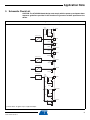
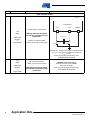
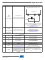
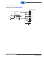
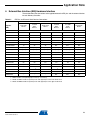
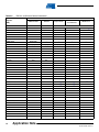
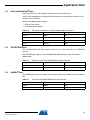
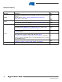
AT91SAM9G45 Microcontroller Schematic
Check List
1. Introduction
This application note is a schematic review check list for systems embedding the
Atmel® ARM® Thumb®-based AT91SAM9G45 microcontroller.
It gives requirements concerning the different pin connections that must be considered before starting any new board design and describes the minimum hardware
resources required to quickly develop an application with the AT91SAM9G45. It does
not consider PCB layout constraints.
AT91 ARM
Thumb-based
Microcontrollers
It also gives advice regarding low-power design constraints to minimize power
consumption.
This application note is not intended to be exhaustive. Its objective is to cover as
many configurations of use as possible.
Application Note
The Check List table has a column reserved for reviewing designers to verify the line
item has been checked.
6494D–ATARM–09-Mar-10
2. Associated Documentation
Before going further into this application note, it is strongly recommended to check the latest
documents for the AT91SAM9G45 Microcontroller on Atmel’s Web site.
Table 2-1 gives the associated documentation needed to support full understanding of this application note.
Table 2-1.
Associated Documentation
Information
Document Title
User Manual
Electrical/Mechanical Characteristics
Ordering Information
Errata
AT91 ARM Thumb-based Microcontrollers - AT91SAM9G45 Preliminary
Datasheet
Internal architecture of processor
ARM/Thumb instruction sets
Embedded in-circuit-emulator
ARM9EJ-S™ Technical Reference Manual
ARM926EJ-S™ Technical Reference Manual
Evaluation Kit User Guide
AT91SAM9G45-EKES User Guide
Using SDRAM on AT91SAM9 Microcontrollers
Using SDRAM on AT91SAM9 Microcontrollers Application Note
NAND Flash Support in AT91SAM9 Microcontrollers
NAND Flash Support in AT91SAM9 Microcontrollers Application Note
Implementation of DDR2 on AT91SAM9G45 Devices
Implementation of DDR2 on AT91SAM9G45 Devices Application Note
2
Application Note
6494D–ATARM–09-Mar-10
Application Note
3. Schematic Check List
CAUTION: The AT91SAM9 board design must comply with the power-up and power-down
sequence guidelines provided in the datasheet to guarantee reliable operation of the
device.
1.0V, 1.8V and 3.3V Power Supplies Schematic Example(1)
10µH
VDDOSC
1R
100nF
4.7µF
DC/DC Converter
GNDOSC
VDDANA
100nF
3.3V
GNDANA
VDDBU
100nF
GNDBU
VDDIOP0,1,2
100nF
GNDIOP
VDDUTMII
100nF
GNDUTMI
DC/DC Converter
VDDIOM0,1
100nF
1.8V
GNDIOM
DC/DC Converter
VDDCORE
100nF
1V
GNDCORE
Linear Regulator
10µH
VDDPLLA
1V
1R
100nF
4.7µF
GNDOSC
10µH
VDDPLLUTMI
1R
100nF
4.7µF
GNDOSC
VDDUTMIC
2.2µF
100nF
GND
(1)
These values are given only as a typical example
3
6494D–ATARM–09-Mar-10
;
Signal Name
Recommended Pin Connection
Description
Powers the device.
VDDCORE
0.9V to 1.1V
Decoupling capacitor (100 nF)(1)(2)
Decoupling/Filtering capacitors must be added to improve
startup stability and reduce source voltage drop.
Supply ripple must not exceed 20 mVrms.
Powers the PLLA cell.
VDDPLLA
0.9V to 1.1V
Decoupling/filtering RLC circuit(1)
The VDDPLLA power supply pin draws small current, but it
is noise sensitive. Care must be taken in VDDPLLA power
supply routing, decoupling and also on bypass capacitors.
Supply ripple must not exceed 10 mVrms.
Powers the PLLUTMI cell.
VDDPLLUTMI
0.9V to 1.1V
Decoupling/filtering RLC circuit(1)
The VDDPLLUTMI power supply pin draws small current,
but it is noise sensitive. Care must be taken in
VDDPLLUTMI power supply routing, decoupling and also
on bypass capacitors.
Supply ripple must not exceed 10 mVrms.
VDDBU
1.8V to 3.6V
Decoupling capacitor (100 nF)(1)(2)
Powers the Backup unit.
(Slow Clock Oscillator, On-chip RC and a part of the
System Controller).
Supply ripple must not exceed 30 mVrms.
Powers the main oscillator cells.
1.65V to 3.6V
VDDOSC
Decoupling/Filtering RLC circuit(1)
The VDDOSC power supply pin draws small current, but it
is noise sensitive. Care must be taken in VDDOSC power
supply routing, decoupling and also on bypass capacitors.
Supply ripple must not exceed 30 mVrms.
1.65V to 1.95V
Decoupling capacitor (100 nF)(1)(2)
VDDIOM0
If the DDRSDR Controller is not used,
VDDIOM0 must be tied to GNDIOM.
Power the DDR2/LPDDR I/O lines.
Decoupling/Filtering capacitors must be added to improve
startup stability and reduce source voltage drop.
Powers the External Bus Interface I/O lines.
VDDIOM1
1.65V to 1.95V
or
3.0V to 3.6V
Decoupling capacitor (100 nF)(1)(2)
Dual voltage range supported.
The I/O drives are selected by programming the
EBI_DRIVE field in the CCFG_EBICSA register.
At power-up, the high drive mode for 3.3V memories is
selected.
Decoupling/Filtering capacitors must be added to improve
startup stability and reduce source voltage drop.
4
Application Note
6494D–ATARM–09-Mar-10
Application Note
;
Signal Name
Recommended Pin Connection
Description
VDDUTMII
3V to 3.6V
Decoupling capacitor (100 nF)(1)(2)
VDDUTMIC
0.9V to 1.1V
Decoupling/Filtering capacitors
(100 nF and 2.2µF)(1)(2)
VDDIOP0
VDDIOP1
VDDIOP2
1.65V to 3.6V
Decoupling/Filtering capacitors
(100 nF)(1)(2)
VDDANA
3.0V to 3.6V
Decoupling/Filtering RLC circuit(1)
Application dependent
Powers the Analog to Digital Converter (ADC) and some
PIOD I/O lines.
GNDCORE
Core Chip Ground
GNDCORE pins are common to VDDCORE pins.
GNDCORE pins should be connected as shortly as
possible to the system ground plane.
GNDBU
Backup Ground
GNDBU pin is provided for VDDBU pins.
GNDBU pin should be connected as shortly as possible to
the system ground plane.
DDR2 and EBI I/O Lines Ground
GNDIOM pins are common to VDDIOM0 and VDDIOM1
pins.
GNDIOM pins should be connected as shortly as possible
to the system ground plane.
Peripherals and ISI I/O lines Ground
GNDIOP pins are common to VDDIOP0, VDDIOP1 and
VDDIOP2 pins.
GNDIOP pins should be connected as shortly as possible
to the system ground plane.
GNDOSC
PLLA, PLLUTMI and Oscillator Ground
GNDOSC pin is provided for VDDOSC, VDDPLLA and
VDDPLLUTMI pins.
GNDOSC pin should be connected as shortly as possible
to the system ground plane.
GNDUTMI
UDPHS and UHPHS UTMI+ Core and
interface Ground
GNDUTMI pins are common to VDDUTMII and
VDDUTMIC pins.
GNDUTMI pins should be connected as shortly as possible
to the system ground plane.
GNDANA
Analog Ground
GNDANA pins are common to VDDANA pins.
GNDANA pins should be connected as shortly as possible
to the system ground plane.
Powers the USB device and host UTMI+ interface.
GNDIOM
GNDIOP
Decoupling/Filtering capacitors must be added to improve
startup stability and reduce source voltage drop.
Powers the USB device and host UTMI+ core.
Decoupling/Filtering capacitors must be added to improve
startup stability and reduce source voltage drop.
Powers the peripherals I/O lines.
Decoupling/Filtering capacitors must be added to improve
startup stability and reduce source voltage drop.
5
6494D–ATARM–09-Mar-10
;
Signal Name
Recommended Pin Connection
Description
Clock, Oscillator and PLL
Crystal load capacitance to check (CCRYSTAL).
AT91SAM9G45
XOUT
XIN
GNDOSC
Crystals between 8 and 16 MHz
XIN
XOUT
12MHz Main
Oscillator
in
Normal Mode
USB High Speed (not Full Speed)
Host and Device peripherals need a
12 Mhz clock.
Capacitors on XIN and XOUT
(crystal load capacitance dependent)
CCRYSTAL
CLEXT
CLEXT
Example: for a 12 MHz crystal with a load capacitance of
CCRYSTAL= 15 pF, external capacitors are required:
CLEXT = 22 pF.
Refer to the electrical specifications of the
AT91SAM9G45 Datasheet
XIN
XOUT
12MHz Main
Oscillator
in
Bypass Mode
6
XIN: external clock source
XOUT: can be left unconnected
USB High speed (not Full Speed)
Host and Device peripherals need a
12 Mhz clock.
VDDOSC square wave signal
External clock source up to 50 MHz
Duty Cycle: 40 to 60%
Refer to the electrical specifications of the
AT91SAM9G45 Datasheet
Application Note
6494D–ATARM–09-Mar-10
Application Note
;
Signal Name
Recommended Pin Connection
Description
Crystal load capacitance to check (CCRYSTAL32).
AT91SAM9G45
XIN32
XIN32
XOUT32
Slow Clock Oscillator
32.768 kHz Crystal
XOUT32
GNDBU
C CRYSTAL32
Capacitors on XIN32 and XOUT32
(crystal load capacitance dependent)
CLEXT32
CLEXT32
Example: for a 32.768 kHz crystal with a load capacitance
of CCRYSTAL32= 12.5 pF, external capacitors are required:
CLEXT32 = 19 pF.
Refer to the electrical specifications of the
AT91SAM9G45 Datasheet
XIN32
XOUT32
Slow Clock Oscillator
in
Bypass Mode
XIN32: external clock source
XOUT32: can be left unconnected
VDDBU square wave signal
External clock source up to 44 kHz
Refer to the electrical specifications of the
AT91SAM9G45 Datasheet
ICE and JTAG(3)
TCK
Pull-up (100 kOhm)(1)
This pin is a Schmitt trigger input.
No internal pull-up resistor.
TMS
Pull-up (100 kOhm)(1)
This pin is a Schmitt trigger input.
No internal pull-up resistor.
TDI
Pull-up (100 kOhm)(1)
This pin is a Schmitt trigger input.
No internal pull-up resistor.
TDO
Floating
Output driven at up to VVDDIOP0
RTCK
Floating
Output driven at up to VVDDIO0P
NTRST
Please refer to the I/O line
considerations and the errata sections
of the AT91SAM9G45 Datasheet
This pin is a Schmitt trigger input.
Internal pull-up resistor to VVDDIOP0 (100 kOhm).
JTAGSEL
In harsh environments,(4) It is
strongly recommended to tie this
pin to GNDBU if not used or to add
an external low-value resistor (such
as 1 kOhm).
Internal pull-down resistor to GNDBU (15 kOhm).
Must be tied to VVDDBU to enter JTAG Boundary Scan.
7
6494D–ATARM–09-Mar-10
;
Signal Name
Recommended Pin Connection
Description
Reset/Test
NRST is a bidirectional pin (Schmitt trigger input).
It is handled by the on-chip reset controller and can
be driven low to provide a reset signal to the external
NRST
Application dependent.
Can be connected to a push button for
hardware reset.
components or asserted low externally to reset the
microcontroller.
By default, the User Reset is enabled after a General
Reset so that it is possible for a component to assert low
and reset the microcontroller.
An internal pull-up resistor to VVDDIOP0 (100 kOhm) is
available for User Reset and External Reset control.
TST
In harsh environments,(4) It is
strongly recommended to tie this
pin to GNDBU if not used or to add
an external low-value resistor (such
as 1 kOhm)
This pin is a Schmitt trigger input.
Internal pull-down resistor to GNDBU (15 kOhm).
Must be tied to VVDDIOP0 to boot from Embedded ROM.
BMS
Application dependent.
Must be tied to GNDIOP to boot from external memory
(EBI Chip Select 0).
Shutdown/Wakeup Logic
SHDN
Application dependent.
A typical application connects the pin
SHDN to the shutdown input of the
DC/DC Converter providing the main
power supplies.
This pin is a push-pull output.
SHDN pin is driven low to GNDBU by the Shutdown
Controller (SHDWC).
WKUP
0V to VVDDBU
This pin is an input-only.
WKUP behavior can be configured through the Shutdown
Controller (SHDWC).
PIO
PAx
PBx
PCx
All PIOs are pulled-up inputs (100 kOhms) at reset except
those which are multiplexed with the Address Bus signals
that require to be enabled as peripherals:
Refer to the column “Reset State” of the PIO Controller
multiplexing tables in the product datasheet.
Application dependent.
Schmitt Trigger on All Inputs
To reduce power consumption if not used, the concerned
PIO can be configured as an output, driven at ‘0’ with
internal pull-up disabled.
ADC
TSADVREF
8
2.4V to VDDANA
Decoupling/Filtering capacitors.
Application dependent
ADVREF is a pure analog input.
To reduce power consumption, if ADC is not used:
connect ADVREF to GNDANA.
Application Note
6494D–ATARM–09-Mar-10
Application Note
;
Signal Name
Recommended Pin Connection
Description
EBI
Data Bus (D0 to D31)
All data bus lines are pulled-up inputs to VVDDIOM1 at reset.
D0-D31
Application dependent.
Note:
D16 to D31 are multiplexed with the PIOC
controller.
Address Bus (A0 to A25)
All address lines are driven to ‘0’ at reset.
A0-A25
Application dependent.
Note:
A19 to A25 are multiplexed with the PIOC
controller.
DDR Memory Interface- DDR2/SDRAM/LPDDR Controller
Application dependent.
DDR_D0-DDR_D15
If the DDRSDR Controller is not used,
DDR_D0-DDR_D15 pins can be left
unconnected.
Data Bus
Data bus lines are pulled-up inputs to VVDDIOM0 at reset.
Application dependent.
DDR_A0-DDR_A13
If the DDRSDR Controller is not used,
DDR_A0-DDR_A13 pins can be left
unconnected.
Address Bus
All address lines are driven to ‘0’ at reset.
If the DDR2 Controller is used with
LPDDR or DDR2 memory,
DDR_VREF is connected to
VDDIOM0/2 (i.e. 0.9V)
DDR_VREF
If the DDR2 Controller is used with an
SDRAM memory, DDR_VREF is
connected to GND or VDDIOM0/2.
Reference voltage for DDR2 Controller.
If the DDR2 Controller is not used, DDR_VREF is
connected to GND.
SMC - SDRAM Controller - CompactFlash® Support - NAND Flash Support
See “External Bus Interface (EBI) Hardware Interface” on page 13.
USB High Speed Host (UHPHS)
HFSDPA/HFSDPB
HHSDPA/HHSDPB
Application dependent.(5)
Integrated pull-down resistor to prevent over consumption
when the host is disconnected.
HFSDMA/HFSDMB
HHSDMA/HHSDMB
Application dependent.(5)
Integrated pull-down resistor to prevent over consumption
when the host is disconnected.
9
6494D–ATARM–09-Mar-10
;
Signal Name
Recommended Pin Connection
Description
USB High Speed Device (UDPHS)
DHSDM/DFSDP
Application dependent(6)
Integrated programmable pull-up resistor.
Integrated programmable pull-down resistor to prevent
over consumption when the host is disconnected.
To reduce power consumption, if USB Device is not used,
connect the embedded pull-up.
Integrated programmable pull-down resistor to prevent
over consumption when the host is disconnected.
DHSDP/DFSDM
Application dependent(6)
To reduce power consumption, if USB Device is not used,
connect the embedded pull-down.
10
Application Note
6494D–ATARM–09-Mar-10
Application Note
Notes:
1. These values are given only as a typical example.
2. Decoupling capacitors must be connected as close as possible to the microcontroller and on each concerned pin.
100nF
VDDCORE
100nF
VDDCORE
100nF
VDDCORE
GND
3. It is recommended to establish accessibility to a JTAG connector for debug in any case.
4. In a well-shielded environment subject to low magnetic and electric field interference, the pin may be left unconnected. In
noisy environments, a connection to ground is recommended.
5. Example of USB High Speed Host connection:
A termination 39 Ohm serial resistor must be connected to HFSDPx and HFSDMx. More details are in the USB High Speed
Host Port section of the AT91SAM9G45 Datasheet.
PIO (VBUS DETECT)
15k Ω
(1)
"A" Receptacle
1 = VBUS
2 = D3 = D+
4 = GND
HHSDM
39 ± 5% Ω
HFSDM
3 4
(1)
22k Ω
Shell = Shield
HHSDP
CRPB
1 2
39 ± 5% Ω
CRPB: 1µF to 10µF
HFSDP
6K8 ± 1% Ω
VBG
10 pF
GND
11
6494D–ATARM–09-Mar-10
6. Typical USB High Speed Device connection:
As there is an embedded pull-up, no external circuitry is necessary to enable and disable the 1.5 k Ohm pull-up.
A termination 39 Ohm serial resistor must be connected to DFSDP and DFSDM. More details are in the USB High Speed
Device Port section of the AT91SAM9G45 Datasheet.
PIO (VBUS DETECT)
15k Ω
"B" Receptacle
1 = VBUS
2 = D3 = D+
4 = GND
1
DHSDM
39 ± 5% Ω
DFSDM
2
Shell = Shield
22k Ω
CRPB
3
DHSDP
4
39 ± 5% Ω
CRPB:1µF to 10µF
DFSDP
6K8 ± 1% Ω
VBG
10 pF
GND
12
Application Note
6494D–ATARM–09-Mar-10
Application Note
4. External Bus Interface (EBI) Hardware Interface
These tables detail the connections to be applied between the EBI pins and the external devices
for each Memory Controller.
Table 4-1.
EBI Pins and External Static Devices Connections
Pins of the Interfaced Device
8-bit Static
Device
Signals:
EBI_
2 x 8-bit
Static
Devices
16-bit Static
Device
Controller
4 x 8-bit
Static
Devices
2 x 16-bit
Static
Devices
32-bit Static
Device
SMC
D0 - D7
D0 - D7
D0 - D7
D0 - D7
D0 - D7
D0 - D7
D0 - D7
D8 - D15
–
D8 - D15
D8 - D15
D8 - D15
D8 - 15
D8 - 15
D16 - D23
–
–
–
D16 - D23
D16 - D23
D16 - D23
D24 - D31
–
–
–
D24 - D31
D24 - D31
D24 - D31
A0/NBS0
A0
A1/NWR2/NBS2
–
NLB
–
(2)
BE0
NLB
(4)
BE2
A1
A0
A0
A[2:22]
A[1:21]
A[1:21]
A[0:20]
A[0:20]
A[0:20]
A[23:25]
A[22:24]
A[22:24]
A[21:23]
A[21:23]
A[21:23]
NCS0
CS
CS
CS
CS
CS
CS
NCS1/DDRSDCS
CS
CS
CS
CS
CS
CS
NCS2
CS
CS
CS
CS
CS
CS
NCS3/NANDCS
CS
CS
CS
CS
CS
CS
NCS4/CFCS0
CS
CS
CS
CS
CS
CS
NCS5/CFCS1
CS
CS
CS
CS
CS
CS
NRD/CFOE
OE
OE
OE
OE
OE
OE
WE
WE
A2 - A22
A23 - A25
(5)
NWR0/NWE
NWR1/NBS1
NWR3/NBS3
Notes:
1.
2.
3.
4.
WE
–
–
WE
(1)
WE
(1)
–
WE
NUB
–
WE
NLB
(3)
WE
(2)
WE
(2)
WE
(2)
NUB
(3)
BE1
NUB
(4)
BE3
NWR0 enables lower byte writes. NWR1 enables upper byte writes.
NWRx enables corresponding byte x writes (x = 0,1,2 or 3).
NBS0 and NBS1 enable respectively lower and upper bytes of the lower 16-bit word.
NBS2 and NBS3 enable respectively lower and upper bytes of the upper 16-bit word.
13
6494D–ATARM–09-Mar-10
Table 4-2.
EBI Pins and External Device Connections
Pins of the Interfaced Device
Signals:
EBI_
Controller
DDR2/LPDDR
SDRAM
DDRC
SDRAMC
CompactFlash
CompactFlash
True IDE Mode
NAND Flash
SMC
D0 - D7
D0 - D7
D0 - D7
D0 - D7
D0 - D7
I/O0-I/O7
D8 - D15
D8 - D15
D8 - D15
D8 - 15
D8 - 15
I/O8-I/O15(4)
D16 - D31
–
D16 - D31
–
–
–
A0/NBS0
–
–
A0
A0
–
A1/NWR2/NBS2
–
–
A1
A1
–
DQM0-DQM3
DQM0-DQM3
DQM0-DQM3
–
–
–
DQS0-DQM1
DQS0-DQS1
–
–
–
–
A[0:8]
A[0:8]
A[2:10]
A[2:10]
–
A9
A9
–
–
–
–
A10
–
–
–
A2 - A10
A11
SDA10
A12
A13 - A14
–
–
–
–
–
A[11:12]
A[11:12]
–
–
–
A15
A13
A13
–
–
–
A16/BA0
BA0
BA0
–
–
–
A17/BA1
BA1
BA1
–
–
–
A18 - A20
–
–
–
–
–
A21/NANDALE
–
–
–
–
ALE
A22/NANDCLE
–
–
REG
REG
CLE
A23 - A24
–
–
–
–
–
A25
–
–
CFRNW(1)
CFRNW(1)
–
NCS0
NCS1/DDRSDCS
–
–
–
–
–
DDRCS
SDCS
–
–
–
NCS2
–
–
–
–
–
NCS3/NANDCS
–
–
–
–
CE(3)
NCS4/CFCS0
–
–
CFCS0(1)
CFCS0(1)
–
NCS5/CFCS1
–
–
CFCS1(1)
CFCS1(1)
–
NANDOE
–
–
–
–
OE
NANDWE
–
–
–
–
WE
NRD/CFOE
–
–
OE
–
–
NWR0/NWE/CFWE
–
–
WE
WE
–
NWR1/NBS1/CFIOR
–
–
IOR
IOR
–
NWR3/NBS3/CFIOW
–
–
IOW
IOW
–
CFCE1
–
–
CE1
CS0
–
CFCE2
–
–
CE2
CS1
–
SDCK
CK
CLK
–
–
–
SDCK#
CK#
–
–
–
–
SDCKE
CKE
CKE
–
–
–
RAS
RAS
RAS
–
–
–
CAS
CAS
CAS
–
–
–
14
Application Note
6494D–ATARM–09-Mar-10
Application Note
Table 4-2.
EBI Pins and External Device Connections (Continued)
Pins of the Interfaced Device
Signals:
EBI_
Controller
SDWE
(5)
DDR2/LPDDR
SDRAM
DDRC
SDRAMC
WE
WE
CompactFlash
CompactFlash
True IDE Mode
NAND Flash
SMC
–
–
–
–
–
WAIT
WAIT
–
Pxx(2)
–
–
CD1 or CD2
CD1 or CD2
–
(2)
–
–
–
–
CE(3)
Pxx(2)
–
–
–
–
RDY
NWAIT
Pxx
Notes:
1. Not directly connected to the CompactFlash slot. Permits the control of the bidirectional buffer between the EBI data bus and
the CompactFlash slot.
2. Any PIO line.
3. CE connection depends on the NAND Flash.
For standard NAND Flash devices, it must be connected to any free PIO line.
For "CE don't care" NAND Flash devices, it can be either connected to NCS3/NANDCS or to any free PIO line.
4. I/O8 - I/O15 pins used only for 16-bit NAND Flash device.
5. EBI_NWAIT signal is multiplexed with PC15.
15
6494D–ATARM–09-Mar-10
5. AT91SAM Boot Program Hardware Constraints
See the AT91SAM Boot Program section of the AT91SAM9G45 Datasheet for more details on
the boot program.
5.1
AT91SAM Boot Program Supported Crystals (MHz)
A 12 MHz Crystal or external clock (in bypass mode) is mandatory in order to generate USB and
PLL clocks correctly for the following boots.
5.2
NAND Flash Boot
The first block must be guaranteed by the manufacturer. There is no ECC check.
The supported SLC small block NAND Flash devices are described in the Boot Strategies section of the product datasheet.
The NAND Flash boot also supports all the SLC large block NAND Flash devices.
Table 5-1.
5.3
Pins Driven during NAND Flash Boot Program Execution
Peripheral
Pin
PIO Line
EBI CS3 SMC
NANDCS
PC14
EBI CS3 SMC
NAND ALE
A21
EBI CS3 SMC
NAND CLE
A22
EBI CS3 SMC
Cmd//Addr/Data
D[16:0]
SD Card Boot
SD Card Boot supports all SD Card memories compliant with SD Memory Card Specification
V2.0. This includes SDHC cards.
Table 5-2.
16
Pins Driven during SD Card Boot Program Execution
Peripheral
Pin
PIO Line
MCI0
MCI0_CK
PA0
MCI0
MCI0_CD
PA1
MCI0
MCI0_D0
PA2
MCI0
MCI0_D1
PA3
MCI0
MCI0_D2
PA4
MCI0
MCI0_D3
PA5
Application Note
6494D–ATARM–09-Mar-10
Application Note
5.4
Serial and DataFlash® Boot
Two kinds of SPI Flash are supported, SPI Serial Flash and SPI DataFlash.
The SPI Flash bootloader tries to boot on SPI0 Chip Select 0, first looking for SPI Serial Flash,
and then for SPI DataFlash.
The SPI Flash Boot program supports:
• all Serial Flash devices
• all Atmel DataFlash devices.
Table 5-3.
5.5
Pins Driven during Serial or DataFlash Boot Program Execution
Peripheral
Pin
PIO Line
SPI0
MOSI
PB1
SPI0
MISO
PB0
SPI0
SPCK
PB2
SPI0
NPCS0
PB3
TWI EEPROM Boot
The TWI EEPROM Flash Boot program searches for a valid application in an EEPROM
memory.
TWI EEPROM Boot supports all I2C-compatible EEPROM memories using 7 bits device
address 0x50.
Table 5-4.
5.6
Pins Driven during TWI EEPROM Boot Program Execution
Peripheral
Pin
PIO Line
TWI0
TWD0
PA20
TWI0
TWCK0
PA21
SAM-BA® Boot
The SAM-BA Boot Assistant supports serial communication via the DBGU or the USB Device
Port.
Table 5-5.
Pins Driven during SAM-BA Boot Program Execution
Peripheral
Pin
PIO Line
DBGU
DRXD
PB12
DBGU
DTXD
PB13
17
6494D–ATARM–09-Mar-10
Revision History
Change Request
Ref.
Doc. Rev
Comments
7064
6494D
‘XIN XOUT 12MHz Main Oscillator in Normal Mode’ edited: text removed and figure
updated.
Row A15 edited in Table 4-2, “EBI Pins and External Device Connections”.
“DDR_VREF” contents edited.
Supply ripple unit ‘mV’ changed into ‘mVrms’
6831
Only 1 capacitor value in front of VDDIOP in Section 3. “Schematic Check List” table
6868
A new reference at the bottom of Table 2-1, “Associated Documentation”
6775
Note added to “VDDIOM0” signal in table.
Note added to “DDR_D0-DDR_D15”and “DDR_A0-DDR_A13” signals in “DDR
Memory Interface- DDR2/SDRAM/LPDDR Controller” table part
6736
DDR_VREF signal added to “DDR Memory Interface- DDR2/SDRAM/LPDDR
Controller” table part
6734
EBI CS0 changed into EBI CS3 in Table 5-1
TWI, TWD, TWCK changed into TWI0, TWD0, TWCK0 in Table 5-4
In Section 5.1 “AT91SAM Boot Program Supported Crystals (MHz)”, ‘NAND Flash
memory’ changed into ‘EEPROM memory’, and ‘TWI EEPROM memories’ changed
into ‘EEPROM memories’.
rfo
In Section 3. “Schematic Check List”, Supply Voltage Ripple information added to
“VDDCORE”, “VDDPLLA”, “VDDPLLUTMI”, “VDDBU” and “VDDOSC”.
6691
7028
6982
6494C
6494B
6494A
18
First issue
Application Note
6494D–ATARM–09-Mar-10
Headquarters
International
Atmel Corporation
2325 Orchard Parkway
San Jose, CA 95131
USA
Tel: 1(408) 441-0311
Fax: 1(408) 487-2600
Atmel Asia
Unit 1-5 & 16, 19/F
BEA Tower, Millennium City 5
418 Kwun Tong Road
Kwun Tong, Kowloon
Hong Kong
Tel: (852) 2245-6100
Fax: (852) 2722-1369
Atmel Europe
Le Krebs
8, Rue Jean-Pierre Timbaud
BP 309
78054 Saint-Quentin-enYvelines Cedex
France
Tel: (33) 1-30-60-70-00
Fax: (33) 1-30-60-71-11
Atmel Japan
9F, Tonetsu Shinkawa Bldg.
1-24-8 Shinkawa
Chuo-ku, Tokyo 104-0033
Japan
Tel: (81) 3-3523-3551
Fax: (81) 3-3523-7581
Technical Support
AT91SAM Support
Atmel techincal support
Sales Contacts
www.atmel.com/contacts/
Product Contact
Web Site
www.atmel.com
www.atmel.com/AT91SAM
Literature Requests
www.atmel.com/literature
Disclaimer: The information in this document is provided in connection with Atmel products. No license, express or implied, by estoppel or otherwise, to any
intellectual property right is granted by this document or in connection with the sale of Atmel products. EXCEPT AS SET FORTH IN ATMEL’S TERMS AND CONDITIONS OF SALE LOCATED ON ATMEL’S WEB SITE, ATMEL ASSUMES NO LIABILITY WHATSOEVER AND DISCLAIMS ANY EXPRESS, IMPLIED OR STATUTORY
WARRANTY RELATING TO ITS PRODUCTS INCLUDING, BUT NOT LIMITED TO, THE IMPLIED WARRANTY OF MERCHANTABILITY, FITNESS FOR A PARTICULAR
PURPOSE, OR NON-INFRINGEMENT. IN NO EVENT SHALL ATMEL BE LIABLE FOR ANY DIRECT, INDIRECT, CONSEQUENTIAL, PUNITIVE, SPECIAL OR INCIDENTAL DAMAGES (INCLUDING, WITHOUT LIMITATION, DAMAGES FOR LOSS OF PROFITS, BUSINESS INTERRUPTION, OR LOSS OF INFORMATION) ARISING OUT
OF THE USE OR INABILITY TO USE THIS DOCUMENT, EVEN IF ATMEL HAS BEEN ADVISED OF THE POSSIBILITY OF SUCH DAMAGES. Atmel makes no
representations or warranties with respect to the accuracy or completeness of the contents of this document and reserves the right to make changes to specifications and product descriptions at any time without notice. Atmel does not make any commitment to update the information contained herein. Unless specifically provided otherwise, Atmel products are not suitable for, and shall not be used in, automotive applications. Atmel’s products are not intended, authorized, or warranted
for use as components in applications intended to support or sustain life.
© 2010 Atmel Corporation. All rights reserved. Atmel ®, Atmel logo and combinations thereof, DataFlash ®, SAM-BA ® and others are registered
trademarks and others are trademarks of Atmel Corporation or its subsidiaries. ARM ®, the ARM Powered® logo, Thumb ® and others are registered trademarks or trademarks of ARM Ltd. Other terms and product names may be the trademarks of others.
6494D–ATARM–09-Mar-10