1
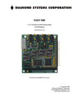
ONYX-MM-XT
PC/104 Format
Counter/Timer & Digital I/O Module
User Manual V1.4
Copyright 2001
Diamond Systems Corporation
8430-D Central Ave.
Newark, CA 94560 USA
Tel (510) 456-7800
Fax (510) 456-7878
[email protected]
Table of Contents
1.
General Information and Features............................................................................................... 3
2.
Onyx-MM Board Drawing ............................................................................................................ 5
3.
I/O Header Pinouts...................................................................................................................... 6
4.
Base Address Configuration ........................................................................................................ 7
5.
Interrupt Configuration ................................................................................................................ 7
6.
Register Map............................................................................................................................... 8
7.
Register definitions...................................................................................................................... 9
8.
Counter/Timer Circuit Schematic .............................................................................................. 13
9.
Interrupt Circuit Schematic........................................................................................................ 14
10.
Specifications............................................................................................................................ 15
Onyx-MM User Manual v1.4
© 2001 Diamond Systems Corporation
2
1. General Information and Features
ONYX-MM is a PC/104-compliant I/O module with 48 digital I/O lines, 3 16-bit counter/timers, and 3
interrupts. It is an 8-bit module, so it does not contain the 16-bit expansion bus connector. This connector
is available as an option by requesting the –B16 suffix when ordering.
Three right-angle pin headers are provided for I/O. Two identical 50-pin (2x25) headers contain 24 digital
I/O lines each and +5/ground, and a third 14-pin (2x7) header provides the counter/timer signals,
external interrupt pin, and +5/ground. J2, with 24 digital I/O lines, is on the right side of the module in the
standard PC/104 I/O position. J3, with 24 additional digital I/O lines, is on the left side of the module, and
J4, with the counter/timer and interrupt signals, is on the top edge of the module. (The bottom edge of
the module is defined as the edge with the PC/104 ISA bus connectors.)
All I/O signals are TTL compatible.
The boards operate on +5V power supply only.
Digital I/O
48 TTL digital I/O lines are provided by 2 82C55 chips (24 per chip). Each line can source 2.5mA in a
logic 0 state and sink 2.5mA in a logic 1 state. I/O lines are unbuffered, i.e. there is a direct connection
between the 82C55 and the I/O header. Bit C0 of each 82C55 can be used to generate an interrupt on
the PC bus (see Interrupts below).
All digital I/O lines are connected to +5V through 10K pull -up resistors.
Digital I/O lines are accessed through two 50-pin headers, J3 and J4, with 24 lines (one 82C55) on each
header. See page 8 for I/O header pinouts.
Counter/Timer I/O
Onyx-MM contains three 16-bit counter/timers provided by an 82C54 chip. Each counter/timer has an
input pin, a gate pin, and an output pin. The input pin responds to positive edges. The gate pin is active
high; a counter will count whenever its associated gate pin is high and will not count when the gate pin is
low. The input and gate pins are connected to +5V through 10K pull -up resistors.
Counter/timer I/O lines are accessed through a 14-pin header J5. See page 8 for the pinout of J5.
An on-board oscillator provides a 4MHz clock that can be used to drive any counter. Each counter has a
maximum input rate of 10MHz.
Programmable features include input source selection and counter cascading:
Counter 0 input can be either IN0 from the I/O header or 4MHz.
Counter 1 input can be either IN1, 4MHz, or Counter 0 output.
Counter 2 input can be either IN2, 4MHz, or Counter 1 output.
All three counter outputs can be programmed to generate PC bus interrupts as described below. With
appropriate configuration, two or three counters can be cascaded to form a 32-bit or 48-bit counter, and
the output of this cascaded counter can generate an interrupt.
Onyx-MM User Manual v1.4
© 2001 Diamond Systems Corporation
3
Interrupts
ONYX-MM provides a means to generate up to three active-high interrupt signals on the PC/104 bus.
Three pin headers are provided to select interrupt levels for each interrupt signal. Interrupt levels 2
through 7 are available on each header.
To enable interrupt sharing, a 1K pull-down resistor can be jumpered to each interrupt line, and
interrupt signals are driven by tristate drivers. When an interrupt is pending, the interrupt line is driven
high, and when it is not pending, the output is in high-impedance mode, and the 1K resistor pulls it
down to a logic 0 state.
Interrupt sources are programmable. Interrupts can be generated from both digital I/O and counter/timer
signals as follows:
Interrupt no. 1:
Interrupt no. 2:
Interrupt no. 3:
Bit C0 from 82C55 #1 or Counter 0 output
Bit C0 from 82C55 #2 or Counter 1 output
External interrupt pin or Counter 2 output
Interrupts are enabled and disabled under software control by manipulating a control register.
Block Diagram
Onyx-MM User Manual v1.4
© 2001 Diamond Systems Corporation
4
2. Onyx-MM Board Drawing
Item
J1
J3
J4
J5
J6
J7
J8
J9
Onyx-MM User Manual v1.4
Description
PC/104 bus connector
Digital I/O ports 1A, 1B, 1C
Digital I/O ports 2A, 2B, 2C
Counter/timer signals
Board base address configuration
Interrupt 0 configuration
Interrupt 1 configuration
Interrupt 2 configuration
© 2001 Diamond Systems Corporation
5
3. I/O Header Pinouts
J3: Digital I/O Header for 82C55 #1
J4: Digital I/O Header for 82C55 #2
Each of these headers is identical in pinout. They provide 24 digital I/O lines, +5, and ground.
Pin 1 of J3 is in the upper right corner of the board, and pin 1 of J4 is in the lower left corner.
A7
A6
A5
A4
A3
A2
A1
A0
C7
C6
C5
C4
C3
C2
C1
C0
B7
B6
B5
B4
B3
B2
B1
B0
+5
1
3
5
7
9
11
13
15
17
19
21
23
25
27
29
31
33
35
37
39
41
43
45
47
49
2
4
6
8
10
12
14
16
18
20
22
24
26
28
30
32
34
36
38
40
42
44
46
48
50
Gnd
Gnd
Gnd
Gnd
Gnd
Gnd
Gnd
Gnd
Gnd
Gnd
Gnd
Gnd
Gnd
Gnd
Gnd
Gnd
Gnd
Gnd
Gnd
Gnd
Gnd
Gnd
Gnd
Gnd
Gnd
J5: Counter/Timer and Interrupt Header
This header is a 14-pin header with all counter/timer signals, the external interrupt pin, +5, and ground.
In 0
Gate 0
Out 0
In 2
Gate 2
Out 2
+5
Onyx-MM User Manual v1.4
1
3
5
7
9
11
13
2
4
6
8
10
12
14
In 1
Gate 1
Out 1
External Interrupt
Gnd
Gnd
Gnd
© 2001 Diamond Systems Corporation
6
4. Base Address Configuration
ONYX-MM's base address is set with header J6, located at the lower right corner of the board. Each of
the six pairs of pins on J6 corresponds to a different address bit. A pair left open is equal to a 1, and a
pair with a jumper installed is equal to a 0. The header is used to select address bits 9-4, resulting in an
16-byte I/O decode. The leftmost pair selects address bit A9, and the rightmost pair selects address bit
A4. Although any 16-byte location is selectable, certain locations are reserved or may cause conflicts.
The table below lists recommended base address settings for ONYX-MM. The default setting is 300 Hex.
"Open" means an open position, and "Inst" means a position with a jumper installed.
Base Address
Hex
Decimal
220
544
240
576
250
592
260
608
280
640
290
656
2A0
672
2B0
688
2C0
704
2D0
720
2E0
736
300
768 (Default)
330
816
340
832
350
848
360
864
380
896
390
912
3A0
928
3C0
960
3E0
992
9
Open
Open
Open
Open
Open
Open
Open
Open
Open
Open
Open
Open
Open
Open
Open
Open
Open
Open
Open
Open
Open
Header J6 Position
8
7
6
Inst
Inst
Inst
Inst
Inst
Open
Inst
Inst
Open
Inst
Inst
Open
Inst
Open Inst
Inst
Open Inst
Inst
Open Inst
Inst
Open Inst
Inst
Open Open
Inst
Open Open
Inst
Open Open
Open Inst
Inst
Open Inst
Inst
Open Inst
Open
Open Inst
Open
Open Inst
Open
Open Open Inst
Open Open Inst
Open Open Inst
Open Open Open
Open Open Open
5
Open
Inst
Inst
Open
Inst
Inst
Open
Open
Inst
Inst
Open
Inst
Open
Inst
Inst
Open
Inst
Inst
Open
Inst
Open
4
Inst
Inst
Open
Inst
Inst
Open
Inst
Open
Inst
Open
Inst
Inst
Open
Inst
Open
Inst
Inst
Open
Inst
Inst
Inst
5. Interrupt Configuration
Each interrupt signal has its own configuration jumper block. The jumper block configures the interrupt
level and the 1K Ohm pull-down resistor. A pull-down resistor is required on each active interrupt line on
the PC/104 bus. Only one resistor should be installed per interrupt level for the entire system.
J7: Interrupt #0
J8: Interrupt #1
J9: Interrupt #2
Position
R
7
6
5
4
3
2
Function
1K Ohm Resistor
IRQ7
IRQ6
IRQ5
IRQ4
IRQ3
IRQ2
Open
No pulldown
Jumper
Pulldown (max 1 per level)
Install only one jumper in each header
in any of these 6 locations
to select the interrupt level
All three interrupt sources can be set to the same level if desired. However only one pulldown resistor
should be installed for each interrupt level.
Onyx-MM User Manual v1.4
© 2001 Diamond Systems Corporation
7
6. Register Map
Base +
0
1
2
3
4
5
6
7
8
9
10
11
12
13
14
15
Function
DIO port 1A
DIO port 1B
DIO port 1C
DIO port 1 configuration register
DIO port 2A
DIO port 2B
DIO port 2C
DIO port 2 configuration register
Counter/timer 0 data
Counter/timer 1 data
Counter/timer 2 data
Counter/timer mode configuration register
Counter/timer input configuration register
(maps to register 12)
Interrupt configuration register
(maps to register 14)
Comments
0 - 3 are 82C55 #1 registers
4 - 7 are 82C55 #2 registers
8 - 11 are 82C54 registers
Note that locations 12 and 13 both map to the same physical register on Onyx-MM. Likewise locations 14
and 15 both map to the same physical register on the board.
Onyx-MM User Manual v1.4
© 2001 Diamond Systems Corporation
8
7. Register definitions
Base + 0: Digital I/O Register A, 82C55 no. 1
Bit
Name
1A7-1A0
7
6
5
4
3
2
1
0
1A7
1A6
1A5
1A4
1A3
1A2
1A1
1A0
Digital I/O port 1A, port A on 82C55 no. 1
Base + 1: Digital I/O Register B, 82C55 no. 1
Bit
Name
1B7-1B0
7
6
5
4
3
2
1
0
1B7
1B6
1B5
1B4
1B3
1B2
1B1
1B0
Digital I/O port 1B, port B on 82C55 no. 1
Base + 2: Digital I/O Register C, 82C55 no. 1
Bit
Name
1C7-1C0
7
6
5
4
3
2
1
0
1C7
1C6
1C5
1C4
1C3
1C2
1C1
1C0
Digital I/O port 1C, port C on 82C55 no. 1
Base + 4: Digital I/O Register A, 82C55 no. 2
Bit
Name
2A7-2A0
7
6
5
4
3
2
1
0
2A7
2A6
2A5
2A4
2A3
2A2
2A1
2A0
Digital I/O port 2A, port A on 82C55 no. 2
Base + 5: Digital I/O Register B, 82C55 no. 2
Bit
Name
2B7-2B0
7
6
5
4
3
2
1
0
2B7
2B6
2B5
2B4
2B3
2B2
2B1
2B0
Digital I/O port 2B, port B on 82C55 no. 2
Base + 6: Digital I/O Register C, 82C55 no. 2
Bit
Name
2C7-2C0
7
6
5
4
3
2
1
0
2C7
2C6
2C5
2C4
2C3
2C2
2C1
2C0
Digital I/O port 2C, port C on 82C55 no. 2
Onyx-MM User Manual v1.4
© 2001 Diamond Systems Corporation
9
Base + 3: Digital I/O Configuration Register, 82C55 no. 1
Base + 7: Digital I/O Configuration Register, 82C55 no. 2
These control registers determine the direction and mode of the 82C55 digital I/O lines. The diagram
below comes from the 82C55 chip datasheet which is included at the back of this manual. Base + 3 is the
control register for chip 1, and Base + 7 is the control register for chip 2.
Most applications use the simple I/O configuration in which bit 7 is set to 1 and the Mode is set to 0 for all
ports.
Here is a list of common configuration register control bytes:
Configuration Byte
Hex
Decimal
9B
155
92
146
99
153
90
144
8B
139
82
130
89
137
80
128
Onyx-MM User Manual v1.4
Port A
Input
Input
Input
Input
Output
Output
Output
Output
Port B
Input
Input
Output
Output
Input
Input
Output
Output
Port C (both halves)
Input
Output
Input
Output
Input
Output
Input
Output
© 2001 Diamond Systems Corporation
10
Base + 8: Counter/Timer 0 Data
Bit
Name
7
6
5
4
3
2
1
0
D7
D6
D5
D4
D3
D2
D1
D0
D7-D0 Divisor bits 7-0 or 15-8
Base + 9: Counter/Timer 1 Data
Bit
Name
7
6
5
4
3
2
1
0
D7
D6
D5
D4
D3
D2
D1
D0
D7-D0 Divisor bits 7-0 or 15-8
Base + 10: Counter/Timer 2 Data
Bit
Name
7
6
5
4
3
2
1
0
D7
D6
D5
D4
D3
D2
D1
D0
D7-D0 Divisor bits 7-0 or 15-8
Base + 11: Counter/Timer Configuration
The diagram below is from the 82C54 datasheet which is included at the back of this manual.
Onyx-MM User Manual v1.4
© 2001 Diamond Systems Corporation
11
The registers described below are built in to the Onyx-MM circuitry and are separate from the 82C55 and
82C54 chips. In the register maps below, blank locations are unused. See the accompanying schematic
diagrams on the following pages.
Base + 12: Counter/timer input configuration register
Bit
7
6
5
4
3
2
1
0
S21
S20
S11
S10
S0
5
4
3
2
1
0
SRC2
SRC1
SRC0
INTE2
INTE1
INTE0
Name
S21 - S20
Counter 2 input select:
S21
0
0
1
S11 - S10
S20
0
1
X
Counter 1 input select:
S11
0
0
1
S0
Input source
In2
4MHz oscillator
Out1
S10
0
1
X
Input source
In1
4MHz oscillator
Out0
Counter 0 input select
0
In0
1
4MHz oscillator
Base + 14: Interrupt configuration register
Bit
7
Name
6
SRC2
Interrupt source 2:
0
External interrupt pin
1
Counter 2 output
SRC1
Interrupt source 1:
0
Bit C0 from 82C55 #2 (base + 6, bit 0)
1
Counter 1 output
SRC0
Interrupt source 0:
0
Bit C0 from 82C55 #1 (base + 2, bit 0)
1
Counter 0 output
INTE2 - 0
Interrupt enable signals
0
Disabled
1
Enabled
Onyx-MM User Manual v1.4
© 2001 Diamond Systems Corporation
12
8. Counter/Timer Circuit Schematic
The schematic below illustrates the counter/timer configuration and how the counter/timer input
configuration register controls it. See the control register description on page 12.
Onyx-MM User Manual v1.4
© 2001 Diamond Systems Corporation
13
9. Interrupt Circuit Schematic
The schematic below illustrates the interrupt circuit configuration and how the interrupt configuration
register controls it. See the control register description on page 12.
Onyx-MM User Manual v1.4
© 2001 Diamond Systems Corporation
14
10. Specifications
Counter/Timer Circuitry
Chip
82C54-2
Counter/timers
3, 16 bits wide
Maximum input frequency
10MHz
On-board oscillator
4MHz ± .01% (100 ppm)
Signal type
TTL
Input voltage, all inputs:
Low
High
-0.5V min, 0.8V max
2.0V min, 5.5V max
Input current
-200A max (low), 2A max (high)
Output voltage, all outputs:
Low
High
0.0V min, 0.4V max
3.0V min, Vcc - 0.4V max
Output current
±2.5mA max, each line
Pullup resistors
10K all input lines
Digital I/O Circuitry
Chip
82C55A (x2)
Number of I/O lines
48
Direction
All lines programmable for input or output in groups of 4/8
Input voltage:
Low
High
-0.5V min, 0.8V max
2.0V min, 5.5V max
Output voltage:
Low
High
0.0V min, 0.4V max
3.0V min, Vcc - 0.4V max
Output current
±2.5mA max, each line
Pullup resistors
10K all lines
Interrupt Circuitry
No. of interrupts
3
Pull-down resistor
1K resistor selectable via jumper on each interrupt
Interrupt levels
2-7
General
Dimensions
3.550” x 3.775”
Power supply (Vcc)
5.0VDC ±10%, 200mA typical (all outputs open)
Card type
8-bit PC/104 bus compliant
Temperature range
-40 - +85 C, operating and storage
Onyx-MM User Manual v1.4
o
© 2001 Diamond Systems Corporation
15
82C55A
CMOS Programmable
Peripheral Interface
June 1998
Features
Description
• Pin Compatible with NMOS 8255A
The Intersil 82C55A is a high performance CMOS version of
the industry standard 8255A and is manufactured using a
self-aligned silicon gate CMOS process (Scaled SAJI IV). It
is a general purpose programmable I/O device which may be
used with many different microprocessors. There are 24 I/O
pins which may be individually programmed in 2 groups of
12 and used in 3 major modes of operation. The high
performance and industry standard configuration of the
82C55A make it compatible with the 80C86, 80C88 and
other microprocessors.
• 24 Programmable I/O Pins
• Fully TTL Compatible
• High Speed, No “Wait State” Operation with 5MHz and
8MHz 80C86 and 80C88
• Direct Bit Set/Reset Capability
• Enhanced Control Word Read Capability
• L7 Process
Static CMOS circuit design insures low operating power. TTL
compatibility over the full military temperature range and bus
hold circuitry eliminate the need for pull-up resistors. The
Intersil advanced SAJI process results in performance equal
to or greater than existing functionally equivalent products at
a fraction of the power.
• 2.5mA Drive Capability on All I/O Ports
• Low Standby Power (ICCSB) . . . . . . . . . . . . . . . . .10µA
Ordering Information
PART NUMBERS
5MHz
8MHz
CP82C55A-5
CP82C55A
IP82C55A-5
IP82C55A
CS82C55A-5
CS82C55A
IS82C55A-5
IS82C55A
CD82C55A-5
CD82C55A
ID82C55A-5
ID82C55A
PACKAGE
40 Ld PDIP
44 Ld PLCC
MD82C55A-5/B MD82C55A/B
8406601QA
8406602QA
40 Ld
CERDIP
8406602XA
PKG.
NO.
0oC to 70oC
E40.6
-40oC to 85oC
E40.6
0oC to 70oC
N44.65
-40oC to 85oC
N44.65
0oC to 70oC
F40.6
-40oC to 85oC
F40.6
-55oC to 125oC
F40.6
SMD#
44 Pad
MR82C55A-5/B MR82C55A/B
CLCC
8406601XA
TEMPERATURE
RANGE
F40.6
-55oC to 125oC
J44.A
SMD#
J44.A
Pinouts
RD
PA0
PA1
PA2
PA3
NC
PA4
PA5
PA6
PA7
WR
34 D3
33 D4
32 D5
31 D6
30 D7
29 NC
CAUTION: These devices are sensitive to electrostatic discharge; follow proper IC Handling Procedures.
http://www.intersil.com or 407-727-9207 | Copyright © Intersil Corporation 1999
1
7
8
9
10
11
12
13
14
15
16
17
39
38
37
36
35
34
33
32
31
30
29
RESET
D0
D1
D2
D3
NC
D4
D5
D6
D7
VCC
18 1920 21 22 23 24 25 26 27 28
PB2
NC
PB3
PB4
PB5
PB6
PB7
37 D0
36 D1
35 D2
6 5 4 3 2 1 44 43 42 41 40
CS
GND
A1
A0
PC7
NC
PC6
PC5
PC4
PC0
PC1
PC2
PC3
PB0
PB1
PA7
PA6
PA5
PA4
PA3
PA2
PA1
PA0
CS
WR
39 NC
38 RESET
NC
VCC
PB7
PB6
PB5
PB4
PB3
PB2
13
14
15
16
17
18
19
20
31
30
29
28
27
26
25
24
23
22
21
82C55A (PLCC)
TOP VIEW
PA4
6 5 4 3 2 1 44 43 42 41 40
PA5
PA6
7
GND
PA7
NC 8
WR
A1 9
RESET
A0 10
D0
PC7 11
D1
PC6 12
D2
PC5 13
D3
PC4 14
D4
PC0 15
D5
PC1 16
D6
PC2 17
D7
18 19 20 21 22 23 24 25 26 27 28
VCC
PB7
PB6
PB5
PB4
PB3
PB1
5
6
7
8
9
10
11
12
40
39
38
37
36
35
34
33
32
PB0
1
2
3
4
PC3
PA3
PA2
PA1
PA0
RD
CS
GND
A1
A0
PC7
PC6
PC5
PC4
PC0
PC1
PC2
PC3
PB0
PB1
PB2
82C55A (CLCC)
TOP VIEW
RD
82C55A (DIP)
TOP VIEW
File Number
2969.2
82C55A
Pin Description
SYMBOL
PIN
NUMBER
VCC
26
VCC: The +5V power supply pin. A 0.1µF capacitor between pins 26 and 7 is
recommended for decoupling.
GND
7
GROUND
D0-D7
27-34
I/O
RESET
35
I
RESET: A high on this input clears the control register and all ports (A, B, C) are set
to the input mode with the “Bus Hold” circuitry turned on.
CS
6
I
CHIP SELECT: Chip select is an active low input used to enable the 82C55A onto the
Data Bus for CPU communications.
RD
5
I
READ: Read is an active low input control signal used by the CPU to read status
information or data via the data bus.
WR
36
I
WRITE: Write is an active low input control signal used by the CPU to load control
words and data into the 82C55A.
A0-A1
8, 9
I
ADDRESS: These input signals, in conjunction with the RD and WR inputs, control
the selection of one of the three ports or the control word register. A0 and A1 are
normally connected to the least significant bits of the Address Bus A0, A1.
PA0-PA7
1-4, 37-40
I/O
PORT A: 8-bit input and output port. Both bus hold high and bus hold low circuitry are
present on this port.
PB0-PB7
18-25
I/O
PORT B: 8-bit input and output port. Bus hold high circuitry is present on this port.
PC0-PC7
10-17
I/O
PORT C: 8-bit input and output port. Bus hold circuitry is present on this port.
TYPE
DESCRIPTION
DATA BUS: The Data Bus lines are bidirectional three-state pins connected to the
system data bus.
Functional Diagram
POWER
SUPPLIES
+5V
GND
GROUP A
PORT A
(8)
GROUP A
CONTROL
GROUP A
PORT C
UPPER
(4)
BI-DIRECTIONAL
DATA BUS
D7-D0
DATA BUS
BUFFER
8-BIT
INTERNAL
DATA BUS
RD
WR
A1
READ
WRITE
CONTROL
LOGIC
GROUP B
CONTROL
GROUP B
PORT C
LOWER
(4)
GROUP B
PORT B
(8)
A0
RESET
CS
2
I/O
PA7-PA0
I/O
PC7-PC4
I/O
PC3-PC0
I/O
PB7-PB0
82C55A
Functional Description
POWER
SUPPLIES
Data Bus Buffer
This three-state bi-directional 8-bit buffer is used to interface
the 82C55A to the system data bus. Data is transmitted or
received by the buffer upon execution of input or output
instructions by the CPU. Control words and status information are also transferred through the data bus buffer.
+5V
GND
BI-DIRECTIONAL
DATA BUS
DATA
BUS
D7-D0
BUFFER
Read/Write and Control Logic
The function of this block is to manage all of the internal and
external transfers of both Data and Control or Status words.
It accepts inputs from the CPU Address and Control busses
and in turn, issues commands to both of the Control Groups.
RD
WR
A1
A0
RESET
READ
WRITE
CONTROL
LOGIC
GROUP A
CONTROL
GROUP A
PORT A
(8)
GROUP A
PORT C
UPPER
(4)
8-BIT
INTERNAL
DATA BUS
GROUP B
CONTROL
GROUP B
PORT C
LOWER
(4)
GROUP B
PORT B
(8)
I/O
PA7PA0
I/O
PC7PC4
I/O
PC3PC0
I/O
PB7PB0
(CS) Chip Select. A “low” on this input pin enables the
communcation between the 82C55A and the CPU.
CS
(RD) Read. A “low” on this input pin enables 82C55A to send
the data or status information to the CPU on the data bus. In
essence, it allows the CPU to “read from” the 82C55A.
FIGURE 1. 82C55A BLOCK DIAGRAM. DATA BUS BUFFER,
READ/WRITE, GROUP A & B CONTROL LOGIC
FUNCTIONS
(WR) Write. A “low” on this input pin enables the CPU to
write data or control words into the 82C55A.
(RESET) Reset. A “high” on this input initializes the control
register to 9Bh and all ports (A, B, C) are set to the input
mode. “Bus hold” devices internal to the 82C55A will hold
the I/O port inputs to a logic “1” state with a maximum hold
current of 400µA.
(A0 and A1) Port Select 0 and Port Select 1. These input
signals, in conjunction with the RD and WR inputs, control
the selection of one of the three ports or the control word
register. They are normally connected to the least significant
bits of the address bus (A0 and A1).
Group A and Group B Controls
82C55A BASIC OPERATION
A1
A0
RD
WR
CS
0
0
0
1
0
The functional configuration of each port is programmed by
the systems software. In essence, the CPU “outputs” a control word to the 82C55A. The control word contains
information such as “mode”, “bit set”, “bit reset”, etc., that initializes the functional configuration of the 82C55A.
INPUT OPERATION
(READ)
Port A → Data Bus
0
1
0
1
0
Port B → Data Bus
1
0
0
1
0
Port C → Data Bus
1
1
0
1
0
Control Word → Data Bus
Each of the Control blocks (Group A and Group B) accepts
“commands” from the Read/Write Control logic, receives
“control words” from the internal data bus and issues the
proper commands to its associated ports.
Control Group A - Port A and Port C upper (C7 - C4)
Control Group B - Port B and Port C lower (C3 - C0)
OUTPUT OPERATION
(WRITE)
0
0
1
0
0
Data Bus → Port A
0
1
1
0
0
Data Bus → Port B
1
0
1
0
0
Data Bus → Port C
1
1
1
0
0
Data Bus → Control
The control word register can be both written and read as
shown in the “Basic Operation” table. Figure 4 shows the
control word format for both Read and Write operations.
When the control word is read, bit D7 will always be a logic
“1”, as this implies control word mode information.
DISABLE FUNCTION
X
X
X
X
1
Data Bus → Three-State
X
X
1
1
0
Data Bus → Three-State
3
82C55A
register will contain 9Bh. During the execution of the system
program, any of the other modes may be selected using a
single output instruction. This allows a single 82C55A to
service a variety of peripheral devices with a simple software
maintenance routine. Any port programmed as an output
port is initialized to all zeros when the control word is written.
Ports A, B, and C
The 82C55A contains three 8-bit ports (A, B, and C). All can
be configured to a wide variety of functional characteristics
by the system software but each has its own special features
or “personality” to further enhance the power and flexibility of
the 82C55A.
ADDRESS BUS
Port A One 8-bit data output latch/buffer and one 8-bit data
input latch. Both “pull-up” and “pull-down” bus-hold devices
are present on Port A. See Figure 2A.
CONTROL BUS
DATA BUS
Port B One 8-bit data input/output latch/buffer and one 8-bit
data input buffer. See Figure 2B.
Port C One 8-bit data output latch/buffer and one 8-bit data
input buffer (no latch for input). This port can be divided into
two 4-bit ports under the mode control. Each 4-bit port contains a 4-bit latch and it can be used for the control signal
output and status signal inputs in conjunction with ports A
and B. See Figure 2B.
C
B
8
A
I/O
PB7-PB0
INPUT MODE
MODE 1
MODE 2
OUTPUT MODE
VCC
I/O
8
I/O
PA7-PA0
A
I/O
8
CONTROL CONTROL
OR I/O
OR I/O
C
I/O
PA7-PA0
A
BIDIRECTIONAL
I/O
PB7-PB0
P
4
PC7-PC4
PC3-PC0
B
8
FIGURE 2A. PORT A BUS-HOLD CONFIGURATION
I/O
C
PB7-PB0
INTERNAL
DATA OUT
(LATCHED)
4
B
8
EXTERNAL
PORT A PIN
RESET
OR MODE
CHANGE
A0-A1
CS
82C55A
MODE 0
MASTER
RESET
OR MODE
CHANGE
INTERNAL
DATA IN
D7-D0
RD, WR
CONTROL
PA7-PA0
FIGURE 3. BASIC MODE DEFINITIONS AND BUS INTERFACE
CONTROL WORD
INTERNAL
DATA IN
D7 D6 D5 D4 D3 D2 D1 D0
EXTERNAL
PORT B, C
PIN
INTERNAL
DATA OUT
(LATCHED)
GROUP B
PORT C (LOWER)
1 = INPUT
0 = OUTPUT
OUTPUT MODE
PORT B
1 = INPUT
0 = OUTPUT
FIGURE 2B. PORT B AND C BUS-HOLD CONFIGURATION
MODE SELECTION
0 = MODE 0
1 = MODE 1
FIGURE 2. BUS-HOLD CONFIGURATION
Operational Description
GROUP A
Mode Selection
PORT C (UPPER)
1 = INPUT
0 = OUTPUT
There are three basic modes of operation than can be
selected by the system software:
Mode 0 - Basic Input/Output
Mode 1 - Strobed Input/Output
Mode 2 - Bi-directional Bus
PORT A
1 = INPUT
0 = OUTPUT
MODE SELECTION
00 = MODE 0
01 = MODE 1
1X = MODE 2
When the reset input goes “high”, all ports will be set to the
input mode with all 24 port lines held at a logic “one” level by
internal bus hold devices. After the reset is removed, the
82C55A can remain in the input mode with no additional initialization required. This eliminates the need to pullup or pulldown resistors in all-CMOS designs. The control word
MODE SET FLAG
1 = ACTIVE
FIGURE 4. MODE DEFINITION FORMAT
4
82C55A
The modes for Port A and Port B can be separately defined,
while Port C is divided into two portions as required by the
Port A and Port B definitions. All of the output registers,
including the status flip-flops, will be reset whenever the
mode is changed. Modes may be combined so that their
functional definition can be “tailored” to almost any I/O
structure. For instance: Group B can be programmed in
Mode 0 to monitor simple switch closings or display computational results, Group A could be programmed in Mode 1 to
monitor a keyboard or tape reader on an interrupt-driven
basis.
This function allows the programmer to enable or disable a
CPU interrupt by a specific I/O device without affecting any
other device in the interrupt structure.
The mode definitions and possible mode combinations may
seem confusing at first, but after a cursory review of the
complete device operation a simple, logical I/O approach will
surface. The design of the 82C55A has taken into account
things such as efficient PC board layout, control signal definition vs. PC layout and complete functional flexibility to support almost any peripheral device with no external logic.
Such design represents the maximum use of the available
pins.
Operating Modes
INTE Flip-Flop Definition
(BIT-SET)-INTE is SET - Interrupt Enable
(BIT-RESET)-INTE is Reset - Interrupt Disable
NOTE: All Mask flip-flops are automatically reset during mode selection and device Reset.
Mode 0 (Basic Input/Output). This functional configuration
provides simple input and output operations for each of the
three ports. No handshaking is required, data is simply written to or read from a specific port.
Mode 0 Basic Functional Definitions:
• Two 8-bit ports and two 4-bit ports
• Any Port can be input or output
Single Bit Set/Reset Feature (Figure 5)
• Outputs are latched
Any of the eight bits of Port C can be Set or Reset using a
single Output instruction. This feature reduces software
requirements in control-based applications.
• Input are not latched
• 16 different Input/Output configurations possible
When Port C is being used as status/control for Port A or B,
these bits can be set or reset by using the Bit Set/Reset
operation just as if they were output ports.
MODE 0 PORT DEFINITION
A
CONTROL WORD
D7 D6 D5 D4 D3 D2 D1 D0
X
X
X
DON’T
CARE
BIT SET/RESET
1 = SET
0 = RESET
BIT SELECT
0 1 2 3 4
0 1 0 1 0
0 0 1 1 0
0 0 0 0 1
5
1
0
1
6
0
1
1
7
1 B0
1 B1
1 B2
BIT SET/RESET FLAG
0 = ACTIVE
FIGURE 5. BIT SET/RESET FORMAT
Interrupt Control Functions
When the 82C55A is programmed to operate in mode 1 or
mode 2, control signals are provided that can be used as
interrupt request inputs to the CPU. The interrupt request
signals, generated from port C, can be inhibited or enabled
by setting or resetting the associated INTE flip-flop, using the
bit set/reset function of port C.
5
B
GROUP A
PORTC
PORT A (Upper)
GROUP B
#
PORTC
PORT B (Lower)
D4
D3
D1
D0
0
0
0
0
Output
Output
0
Output
Output
0
0
0
1
Output
Output
1
Output
Input
0
0
1
0
Output
Output
2
Input
Output
0
0
1
1
Output
Output
3
Input
Input
0
1
0
0
Output
Input
4
Output
Output
0
1
0
1
Output
Input
5
Output
Input
0
1
1
0
Output
Input
6
Input
Output
0
1
1
1
Output
Input
7
Input
Input
1
0
0
0
Input
Output
8
Output
Output
1
0
0
1
Input
Output
9
Output
Input
1
0
1
0
Input
Output
10
Input
Output
1
0
1
1
Input
Output
11
Input
Input
1
1
0
0
Input
Input
12
Output
Output
1
1
0
1
Input
Input
13
Output
Input
1
1
1
0
Input
Input
14
Input
Output
1
1
1
1
Input
Input
15
Input
Input
82C55A
Mode 0 (Basic Input)
tRR
RD
tIR
tHR
INPUT
tAR
tRA
CS, A1, A0
D7-D0
tRD
tDF
Mode 0 (Basic Output)
tWW
WR
tWD
tDW
D7-D0
tAW
tWA
CS, A1, A0
OUTPUT
tWB
Mode 0 Configurations
CONTROL WORD #0
CONTROL WORD #2
D7 D6 D5 D4 D3 D2 D1 D0
1
0
0
0
0
0
0
D7 D6 D5 D4 D3 D2 D1 D0
0
1
8
A
82C55A
4
4
8
B
0
0
0
0
1
0
82C55A
4
PC7 - PC4
PA7 - PA0
PC7 - PC4
C
D7 - D0
4
PC3 - PC0
8
PB7 - PB0
B
PC3 - PC0
PB7 - PB0
CONTROL WORD #3
0
0
D7 D6 D5 D4 D3 D2 D1 D0
1
1
8
A
82C55A
D7 - D0
0
8
D7 D6 D5 D4 D3 D2 D1 D0
0
0
A
CONTROL WORD #1
1
0
PA7 - PA0
C
D7 - D0
0
4
8
B
0
0
0
0
1
1
8
PA7 - PA0
A
82C55A
4
PC7 - PC4
C
4
0
D7 - D0
4
8
B
6
PC7 - PC4
C
PC3 - PC0
PB7 - PB0
PA7 - PA0
PC3 - PC0
PB7 - PB0
82C55A
Mode 0 Configurations
(Continued)
CONTROL WORD #4
CONTROL WORD #8
D7 D6 D5 D4 D3 D2 D1 D0
1
0
0
0
1
0
0
D7 D6 D5 D4 D3 D2 D1 D0
0
1
8
A
82C55A
4
4
8
B
0
0
1
0
0
82C55A
4
8
8
B
0
1
82C55A
PB7 - PB0
0
0
0
1
82C55A
4
PC7 - PC4
PA7 - PA0
PC7 - PC4
C
D7 - D0
4
PC3 - PC0
8
PB7 - PB0
B
PC3 - PC0
PB7 - PB0
D7 D6 D5 D4 D3 D2 D1 D0
1
4
4
8
B
0
0
1
0
0
1
0
8
PA7 - PA0
A
82C55A
4
PC7 - PC4
PA7 - PA0
PC7 - PC4
C
D7 - D0
4
PC3 - PC0
8
PB7 - PB0
B
CONTROL WORD #7
PC3 - PC0
PB7 - PB0
CONTROL WORD #11
D7 D6 D5 D4 D3 D2 D1 D0
0
1
D7 D6 D5 D4 D3 D2 D1 D0
1
1
8
A
82C55A
D7 - D0
1
8
C
D7 - D0
1
0
A
0
8
0
PC3 - PC0
CONTROL WORD #10
A
0
0
PA7 - PA0
D7 D6 D5 D4 D3 D2 D1 D0
0
4
PB7 - PB0
CONTROL WORD #6
1
PC7 - PC4
C
D7 - D0
PC3 - PC0
1
B
1
4
PA7 - PA0
D7 D6 D5 D4 D3 D2 D1 D0
4
0
0
PC7 - PC4
C
D7 - D0
0
0
82C55A
1
8
0
0
CONTROL WORD #9
A
1
0
8
D7 D6 D5 D4 D3 D2 D1 D0
0
1
A
CONTROL WORD #5
1
0
PA7 - PA0
C
D7 - D0
0
4
8
B
0
1
0
0
1
1
8
PA7 - PA0
A
82C55A
4
PC7 - PC4
C
4
0
D7 - D0
4
8
B
7
PC7 - PC4
C
PC3 - PC0
PB7 - PB0
PA7 - PA0
PC3 - PC0
PB7 - PB0
82C55A
Mode 0 Configurations
(Continued)
CONTROL WORD #12
CONTROL WORD #14
D7 D6 D5 D4 D3 D2 D1 D0
1
0
0
1
1
0
0
D7 D6 D5 D4 D3 D2 D1 D0
0
1
8
A
82C55A
4
4
8
B
0
1
1
1
0
1
0
8
82C55A
PA7 - PA0
4
PC7 - PC4
PC7 - PC4
C
D7 - D0
4
PC3 - PC0
PC3 - PC0
8
PB7 - PB0
PB7 - PB0
B
CONTROL WORD #15
D7 D6 D5 D4 D3 D2 D1 D0
0
1
A
CONTROL WORD #13
1
0
PA7 - PA0
C
D7 - D0
0
0
0
D7 D6 D5 D4 D3 D2 D1 D0
1
1
8
A
82C55A
D7 - D0
4
8
B
0
1
1
0
1
1
8
PA7 - PA0
PA7 - PA0
A
82C55A
4
PC7 - PC4
C
4
0
PC7 - PC4
C
D7 - D0
4
PC3 - PC0
PC3 - PC0
8
PB7 - PB0
PB7 - PB0
B
Operating Modes
MODE 1 (PORT A)
Mode 1 - (Strobed Input/Output). This functional configuration provides a means for transferring I/O data to or from a
specified port in conjunction with strobes or “hand shaking”
signals. In mode 1, port A and port B use the lines on port C
to generate or accept these “hand shaking” signals.
CONTROL WORD
D7 D6 D5 D4 D3 D2 D1 D0
1
0
1
1
1/0
INTE
A
PC6, PC7
1 = INPUT
0 = OUTPUT
Mode 1 Basic Function Definitions:
• Two Groups (Group A and Group B)
• Each group contains one 8-bit port and one 4-bit
control/data port
• The 8-bit data port can be either input or output. Both
inputs and outputs are latched.
• The 4-bit port is used for control and status of the 8-bit
port.
8
PA7-PA0
PC4
STBA
PC5
IBFA
INTRA
PC3
RD
PC6, PC7
2
I/O
MODE 1 (PORT B)
CONTROL WORD
D7 D6 D5 D4 D3 D2 D1 D0
Input Control Signal Definition
1
1
1
PB7-PB0
INTE
B
(Figures 6 and 7)
PC2
8
STBB
PC1
IBFB
PC0
INTRB
STB (Strobe Input)
A “low” on this input loads data into the input latch.
RD
IBF (Input Buffer Full F/F)
FIGURE 6. MODE 1 INPUT
A “high” on this output indicates that the data has been
loaded into the input latch: in essence, and acknowledgment. IBF is set by STB input being low and is reset by the
rising edge of the RD input.
8
82C55A
tST
STB
tSIB
IBF
tSIT
tRIB
INTR
tRIT
RD
tPH
INPUT FROM
PERIPHERAL
tPS
FIGURE 7. MODE 1 (STROBED INPUT)
INTR (Interrupt Request)
INTE A
A “high” on this output can be used to interrupt the CPU
when and input device is requesting service. INTR is set by
the condition: STB is a “one”, IBF is a “one” and INTE is a
“one”. It is reset by the falling edge of RD. This procedure
allows an input device to request service from the CPU by
simply strobing its data into the port.
Controlled by Bit Set/Reset of PC6.
INTE B
Controlled by Bit Set/Reset of PC2.
NOTE:
1. To strobe data into the peripheral device, the user must operate
the strobe line in a hand shaking mode. The user needs to send
OBF to the peripheral device, generates an ACK from the peripheral device and then latch data into the peripheral device on
the rising edge of OBF.
INTE A
Controlled by bit set/reset of PC4.
INTE B
MODE 1 (PORT A)
Controlled by bit set/reset of PC2.
PA7-PA0
CONTROL WORD
D7 D6 D5 D4 D3 D2 D1 D0
Output Control Signal Definition
(Figure 8 and 9)
1
0
1
1
1/0
OBF - Output Buffer Full F/F). The OBF output will go “low”
to indicate that the CPU has written data out to be specified
port. This does not mean valid data is sent out of the part at
this time since OBF can go true before data is available.
Data is guaranteed valid at the rising edge of OBF, (See
Note 1). The OBF F/F will be set by the rising edge of the
WR input and reset by ACK input being low.
PC4, PC5
1 = INPUT
0 = OUTPUT
INTE
A
8
PC7
OBFA
PC6
ACKA
INTRA
PC3
WR
ACK - Acknowledge Input). A “low” on this input informs the
82C55A that the data from Port A or Port B is ready to be
accepted. In essence, a response from the peripheral device
indicating that it is ready to accept data, (See Note 1).
PC4, PC5
2
MODE 1 (PORT B)
PB7-PB0
CONTROL WORD
D7 D6 D5 D4 D3 D2 D1 D0
INTR - (Interrupt Request). A “high” on this output can be
used to interrupt the CPU when an output device has
accepted data transmitted by the CPU. INTR is set when
ACK is a “one”, OBF is a “one” and INTE is a “one”. It is
reset by the falling edge of WR.
1
1
PC1
OBFB
PC2
ACKB
PC0
INTRB
0
INTE
B
WR
FIGURE 8. MODE 1 OUTPUT
9
8
82C55A
tWOB
WR
tAOB
OBF
INTR
tWIT
ACK
tAK
tAIT
OUTPUT
tWB
FIGURE 9. MODE 1 (STROBED OUTPUT)
PA7-PA0
RD
CONTROL WORD
D7 D6 D5 D4 D3 D2 D1 D0
1
0
1
1
1/0
1
8
PC4
STBA
PC5
IIBFA
PC6, PC7
1 = INPUT
0 = OUTPUT
PC6, PC7
PB7, PB0
WR
WR
CONTROL WORD
D7 D6 D5 D4 D3 D2 D1 D0
INTRA
PC3
0
PA7-PA0
2
1
0
1
0
1/0
I/O
OBFB
PC2
PC0
PC7
OBFA
PC6
ACKA
INTRA
PC3
1
PC4, PC5
1 = INPUT
0 = OUTPUT
8
PC1
1
8
PC4, PC5
PB7, PB0
2
I/O
8
PC2
STBB
ACKB
PC1
IBFB
INTRB
PC0
INTRB
RD
PORT A - (STROBED INPUT)
PORT B - (STROBED OUTPUT)
PORT A - (STROBED OUTPUT)
PORT B - (STROBED INPUT)
Combinations of Mode 1: Port A and Port B can be individually defined as input or output in Mode 1 to support a wide variety of strobed I/O
applications.
FIGURE 10. COMBINATIONS OF MODE 1
Operating Modes
Mode 2 (Strobed Bi-Directional Bus I/O)
Output Operations
The functional configuration provides a means for communicating with a peripheral device or structure on a single 8-bit
bus for both transmitting and receiving data (bi-directional
bus I/O). “Hand shaking” signals are provided to maintain
proper bus flow discipline similar to Mode 1. Interrupt generation and enable/disable functions are also available.
OBF - (Output Buffer Full). The OBF output will go “low” to
indicate that the CPU has written data out to port A.
Mode 2 Basic Functional Definitions:
• Used in Group A only
• One 8-bit, bi-directional bus Port (Port A) and a 5-bit
control Port (Port C)
• Both inputs and outputs are latched
• The 5-bit control port (Port C) is used for control and
status for the 8-bit, bi-directional bus port (Port A)
INTE 1 - (The INTE flip-flop associated with OBF). Controlled by bit set/reset of PC4.
ACK - (Acknowledge). A “low” on this input enables the
three-state output buffer of port A to send out the data. Otherwise, the output buffer will be in the high impedance state.
Input Operations
STB - (Strobe Input). A “low” on this input loads data into the
input latch.
IBF - (Input Buffer Full F/F). A “high” on this output indicates
that data has been loaded into the input latch.
Bi-Directional Bus I/O Control Signal Definition
INTE 2 - (The INTE flip-flop associated with IBF). Controlled
by bit set/reset of PC4.
(Figures 11, 12, 13, 14)
INTR - (Interrupt Request). A high on this output can be
used to interrupt the CPU for both input or output operations.
10
82C55A
CONTROL WORD
D7 D6 D5 D4 D3 D2 D1 D0
1
1
INTRA
PC3
1/0 1/0 1/0
PA7-PA0
PC2-PC0
1 = INPUT
0 = OUTPUT
PORT B
1 = INPUT
0 = OUTPUT
8
PC7
OBFA
INTE
1
PC6
ACKA
INTE
2
PC4
STBA
PC5
IBFA
WR
GROUP B MODE
0 = MODE 0
1 = MODE 1
PC2-PC0
RD
FIGURE 11. MODE CONTROL WORD
3
I/O
FIGURE 12. MODE 2
DATA FROM
CPU TO 82C55A
WR
tAOB
OBF
tWOB
INTR
tAK
ACK
tST
STB
tSIB
IBF
tAD
tPS
tKD
PERIPHERAL
BUS
tRIB
tPH
RD
DATA FROM
PERIPHERAL TO 82C55A
DATA FROM
82C55A TO PERIPHERAL
DATA FROM
82C55A TO CPU
NOTE: Any sequence where WR occurs before ACK and STB occurs before RD is permissible. (INTR = IBF • MASK • STB • RD ÷ OBF •
MASK • ACK • WR)
FIGURE 13. MODE 2 (BI-DIRECTIONAL)
11
82C55A
MODE 2 AND MODE 0 (INPUT)
MODE 2 AND MODE 0 (OUTPUT)
PC3
PA7-PA0
1
1
0
1
1/0
PC2-PC0
1 = INPUT
0 = OUTPUT
PA7-PA0
8
OBFA
PC7
CONTROL WORD
D7 D6 D5 D4 D3 D2 D1 D0
PC6
ACKA
PC4
STBA
PC5
IBFA
PC2-PC0
PC3
INTRA
3
CONTROL WORD
D7 D6 D5 D4 D3 D2 D1 D0
1
1
0
ACKA
PC4
STBA
IBFA
PC5
3
I/O
8
WR
MODE 2 AND MODE 1 (INPUT)
PC3
PA7-PA0
CONTROL WORD
D7 D6 D5 D4 D3 D2 D1 D0
0
PA7-PA0
8
OBFA
PC6
ACKA
PC4
STBA
PC5
IBFA
PC1
PC3
INTRA
PC7
PB7-PB0
WR
PC6
PB7, PB0
8
MODE 2 AND MODE 1 (OUTPUT)
RD
OBFA
RD
PB7-PB0
1
8
PC7
PC2-PC0
I/O
WR
1
1/0
PC2-PC0
1 = INPUT
0 = OUTPUT
RD
1
0
INTRA
CONTROL WORD
D7 D6 D5 D4 D3 D2 D1 D0
1
1
1
1
OBFB
PC2
ACKB
PC0
INTRB
RD
WR
FIGURE 14. MODE 2 COMBINATIONS
12
8
PC7
OBFA
PC6
ACKA
PC4
STBA
PC5
IBFA
PB7-PB0
8
INTRA
8
PC2
STBB
PC1
IBFB
PC0
INTRB
82C55A
MODE DEFINITION SUMMARY
MODE 1
MODE 0
MODE 2
IN
OUT
IN
OUT
PA0
PA1
PA2
PA3
PA4
PA5
PA6
PA7
In
In
In
In
In
In
In
In
Out
Out
Out
Out
Out
Out
Out
Out
In
In
In
In
In
In
In
In
Out
Out
Out
Out
Out
Out
Out
Out
PB0
PB1
PB2
PB3
PB4
PB5
PB6
PB7
In
In
In
In
In
In
In
In
Out
Out
Out
Out
Out
Out
Out
Out
In
In
In
In
In
In
In
In
Out
Out
Out
Out
Out
Out
Out
Out
PC0
PC1
PC2
PC3
PC4
PC5
PC6
PC7
In
In
In
In
In
In
In
In
Out
Out
Out
Out
Out
Out
Out
Out
INTRB
IBFB
STBB
INTRA
STBA
IBFA
I/O
I/O
INTRB
OBFB
ACKB
INTRA
I/O
I/O
ACKA
OBFA
Special Mode Combination Considerations
GROUP A ONLY
Mode 0
or Mode 1
Only
I/O
I/O
I/O
INTRA
STBA
IBFA
ACKA
OBFA
INPUT CONFIGURATION
There are several combinations of modes possible. For any
combination, some or all of Port C lines are used for control
or status. The remaining bits are either inputs or outputs as
defined by a “Set Mode” command.
D7
D6
D5
I/O
I/O
IBFA
D4
D3
D2
INTEA INTRA INTEB
GROUP A
During a read of Port C, the state of all the Port C lines,
except the ACK and STB lines, will be placed on the data
bus. In place of the ACK and STB line states, flag status will
appear on the data bus in the PC2, PC4, and PC6 bit
positions as illustrated by Figure 17.
D1
D0
IBFB
INTRB
GROUP B
OUTPUT CONFIGURATION
D7
D6
OBFA INTEA
Through a “Write Port C” command, only the Port C pins
programmed as outputs in a Mode 0 group can be written.
No other pins can be affected by a “Write Port C” command,
nor can the interrupt enable flags be accessed. To write to
any Port C output programmed as an output in Mode 1 group
or to change an interrupt enable flag, the “Set/Reset Port C
Bit” command must be used.
D5
D4
I/O
I/O
D3
D2
D1
D0
INTRA INTEB OBFB INTRB
GROUP A
GROUP B
FIGURE 15. MODE 1 STATUS WORD FORMAT
D7
D6
OBFA INTE1
D5
IBFA
D4
INTE2 INTRA
GROUP A
With a “Set/Reset Port Cea Bit” command, any Port C line
programmed as an output (including IBF and OBF) can be
written, or an interrupt enable flag can be either set or reset.
Port C lines programmed as inputs, including ACK and STB
lines, associated with Port C fare not affected by a
“Set/Reset Port C Bit” command. Writing to the corresponding Port C bit positions of the ACK and STB lines with the
“Set Reset Port C Bit” command will affect the Group A and
Group B interrupt enable flags, as illustrated in Figure 17.
D3
D2
D1
D0
X
X
X
GROUP B
(Defined by Mode 0 or Mode 1 Selection)
FIGURE 16. MODE 2 STATUS WORD FORMAT
Current Drive Capability
Any output on Port A, B or C can sink or source 2.5mA. This
feature allows the 82C55A to directly drive Darlington type
drivers and high-voltage displays that require such sink or
source current.
13
82C55A
Reading Port C Status (Figures 15 and 16)
Applications of the 82C55A
In Mode 0, Port C transfers data to or from the peripheral
device. When the 82C55A is programmed to function in
Modes 1 or 2, Port C generates or accepts “hand shaking”
signals with the peripheral device. Reading the contents of
Port C allows the programmer to test or verify the “status” of
each peripheral device and change the program flow
accordingly.
The 82C55A is a very powerful tool for interfacing peripheral
equipment to the microcomputer system. It represents the
optimum use of available pins and flexible enough to interface almost any I/O device without the need for additional
external logic.
Each peripheral device in a microcomputer system usually
has a “service routine” associated with it. The routine
manages the software interface between the device and the
CPU. The functional definition of the 82C55A is programmed
by the I/O service routine and becomes an extension of the
system software. By examining the I/O devices interface
characteristics for both data transfer and timing, and
matching this information to the examples and tables in the
detailed operational description, a control word can easily be
developed to initialize the 82C55A to exactly “fit” the
application. Figures 18 through 24 present a few examples
of typical applications of the 82C55A.
There is not special instruction to read the status information
from Port C. A normal read operation of Port C is executed to
perform this function.
INTERRUPT
ENABLE FLAG
POSITION
ALTERNATE PORT C
PIN SIGNAL (MODE)
INTE B
PC2
ACKB (Output Mode 1)
or STBB (Input Mode 1)
INTE A2
PC4
STBA (Input Mode 1 or
Mode 2)
INTE A1
PC6
ACKA (Output Mode 1 or
Mode 2)
FIGURE 17. INTERRUPT ENABLE FLAGS IN MODES 1 AND 2
INTERRUPT
REQUEST
PC3
PA0
PA1
PA2
PA3
PA4
PA5
MODE 1 PA6
(OUTPUT)
PA7
PC7
PC6
PC5
PC4
HIGH SPEED
PRINTER
HAMMER
RELAYS
DATA READY
ACK
PAPER FEED
FORWARD/REV.
82C55A
PB0
PB1
PB2
PB3
PB4
MODE 1 PB5
(OUTPUT) PB6
PB7
PC1
PC2
PAPER FEED
FORWARD/REV.
RIBBON
CARRIAGE SEN.
DATA READY
ACK
PC0
INTERRUPT
REQUEST
CONTROL LOGIC
AND DRIVERS
FIGURE 18. PRINTER INTERFACE
14